A 24Gb/s Software Programmable Multi-Channel Transmitter · -1 sampling points Called a...
23
A 24Gb/s Software Programmable Multi-Channel Transmitter A Amirkhany 1 A Abbasfar 2 J Savoj 2 M Jeeradit 2 A. Amirkhany 1 , A. Abbasfar 2 , J. Savoj 2 , M. Jeeradit 2 , B. Garlepp 2 , V. Stojanovic 2,3 , M. Horowitz 1,2 1 Stanford University 2 Rambus Inc 3 Massachusetts Institute of Technology
Transcript of A 24Gb/s Software Programmable Multi-Channel Transmitter · -1 sampling points Called a...

A 24Gb/s Software Programmable Multi-Channel Transmitter
A Amirkhany1 A Abbasfar2 J Savoj2 M Jeeradit2A. Amirkhany1, A. Abbasfar2, J. Savoj2, M. Jeeradit2,B. Garlepp2, V. Stojanovic2,3, M. Horowitz1,2
1Stanford University2Rambus Inc
3Massachusetts Institute of Technology

24Gb/s Transmitter
FPGA
Interface
• A test instrument for verifying different transmission
e
• A test instrument for verifying different transmission algorithms
• Multiple operation modes• Multiple operation modes • 2-channel or 4-chanennel Analog Multi-Tone (AMT)
• 2PAM 4PAM 8PAM baseband
2
• 2PAM, 4PAM, 8PAM, … baseband
• Software programmable

High-Speed Electrical Linksg p
PackagePackage
PackagePackage
PackagePackage
PackagePackage
PackagePackage
PackagePackage
PackagePackage
PackagePackage
PackagePackage
PackagePackage
PackagePackage
PackagePackage
PackagePackage
PackagePackage
PackagePackage
PackagePackage
PackagePackage
PackagePackage
PackagePackage
PackagePackage
PackagePackage
PackagePackage
PackagePackage
PackagePackage
PackagePackage
PackagePackage
PackagePackage
PackagePackage
PackagePackage
PackagePackage
PackagePackage
PackagePackage
PackagePackage
PackagePackage
PackagePackage
PackagePackage
PackagePackage
PackagePackage
PackagePackage
PackagePackage
PackagePackage
PackagePackage
PackagePackage
PackagePackage
PackagePackage
PackagePackage
PackagePackage
PackagePackage
augh
ter
card
N t k R tBackplane
Da
Memory cards
Memory cards
Network Routers
Chip A
PCB
Chip B
Package Package
Chip A
PCB
Chip B
Package PackagePackage
Memory controller
PCB
DRA
M
Package
Memory controller
PCB
DRA
M
3
CPU/Controller to DRAM CPU to GPU

State of the Art Links
W1 W2 W3 W4
Line Driver
Rx
Wb1 Wb2 WbkTx
• Baseband 2PAM or 4PAM• 4-5 tap discrete linear transmit equalizer4 5 tap discrete linear transmit equalizer• 5-20 tap decision feedback equalizer (DFE)
4

Channel Characteristics in Links0
Frequency ResponseChip to Chip
-20
-10
dB M lti Drop
-40
-30
d Multi-Drop(Memory)
Backplane
0 5 10 15 20-50
Frequency (GHz)
• Notches caused by reflectionsNotches caused by reflections• From impedance discontinuities
• E.g. vias, stubs, package, parasitic capacitance, etc
5
g , , p g , p p ,
• Multi-Tone signaling can improve performance
A Practical AMT ArchitectureIntegrate
I t t
XN-1
XN-2
ZN-1
ZN-2
Equalizer (WN-1)
E li (W )
N
N Integrate
Integrate
Channel
N 2
X0 Z0
Equalizer (WN-2)
Equalizer (W1)
N
N g
Transmitter Receiver
MIMO DFE
q ( 1)N
• Small number of sub-channels (N)• 2, 3, or 4 in most cases
N ti l d li b h l t th• N-times over-sampled equalizer per sub-channel at the transmitter
• Multi Input Multi Output (MIMO) DFE at the receiver
6
• Multi-Input Multi-Output (MIMO) DFE at the receiver• AMT is a generalization of a baseband system

Two-Channel Example
1.5
3
p
-1
-0.5
0
0.5
1
-1
0
1
2
3
0 0.5 1 1.5 2 2.5 3 3.5 4-1.5
1 2 3 4 5 6 7-3
-2
-0.5
0
0.5
1
1.5
Interference zero at thesampling points
7
0 0.5 1 1.5 2 2.5 3 3.5 4-1.5
-1 sampling pointsCalled a Trans-multiplexer

Evolution of a Baseband Tx Equalizero ut o o a aseba d qua e
w0 w1 w2
x0 x3
w34-tap BB transmitter
w0 w1 w2 w3 0
x1 x2
x2 x
x0
2-way parallelizew0 w1 w2 w3 0
x3
x1
x0
2 way parallelize
w0 w1 w2 w3
w0 w1 w2 w30
0x2
0
x1
Shift “x” to the leftShift “W” to the right
0 1 2 3x3
w0 w1 w2 w3 0x0
2Represent as
8
w0 w1 w2 w30
x2
x3
x1
2
pover-sampled equalizer

AMT is a Generalization of Baseband
4 t B b d 2 Ch l AMT
AMT h d f f d
4-tap Baseband(2-way parallelized)
2-Channel AMT4 taps per channel
• AMT has more degrees of freedom• Better capable of shaping the transmit spectrum
9
• MIMO DFE is also a generalization of a BB DFE

Software Programmable Transmitterg
• Equivalent functionality• 16 tap FIR filter at 12GHz
10
• 16-tap FIR filter at 12GHz
• 2-bit inputs (4PAM) and 10-bit taps

Measured Eye Diagramsy gBaseband Mode AMT Mode
2PAM 2PAM 4PAM Ch1 Ch2 Ch3 Ch4Un-Equalized Equalized Equalized 4-channel AMT (Equalized – Post Processed)
11
12Gb/s 12Gb/s 24Gb/s 18Gb/s
Rx implemented in MatlabOn an oscilloscope

12GS/s Digital to Analog Converterg g
2 t t lti l d• 2-way output multiplexed current-mode DAC
• Termination supply 1.8V• Unused current dumped toUnused current dumped to
1.0V to save power
• 1 8V output swing• 1.8Vpp output swing
12
Savoj, et al, “12GS/s Phase Calibrated CMOS DAC”, Companion paper, Session 7

Digital Equalizer Datapath (One Phase)g ta qua e atapat (O e ase)st
sta
ge
Mux 4x1
Mux
nd s
tage
st s
tage
Mux 4x1
Mux
st s
tage M
ux 4
x1x
4x1
nd s
tage
st s
tage M
ux 4
x1x
4x1
rd s
tage
p p p p p Enco
der
p p p p
Com
p 4:
2 –
1s4x1M
ux 4x1M
u omp
4:2
–2n
Com
p 4:
2 -1
s4x1M
ux 4x1M
u Com
p 4:
2 -1
s
Mux
Mux
4x1
x1omp
4:2
–2n
Com
p 4:
2 -1
s
Mux
Mux
4x1
x1Com
p 4:
2 –
3r
Add
er
Flip
Flo
Flip
Flo
Flip
Flo
Flip
Flo
Flip
Flo
herm
omet
er E
Flip
Flo
Flip
Flo
Flip
Flo
Flip
Flo
• Multiply 16 2-bit numbers by 16 10-bit numbers
Cux 4x1
CCux 4x1
C
Mux
4xC C
Mux
4xC Th
• Multiplication using 4:1 multiplexers• W and 3W stored in flops
• Add results using 4:2 compressor units
13
• Add results using 4:2 compressor units• 2-way parallelized to operate with a 1.5GHz clock

Equalizer Floorplanq p450
output
350
400outputpinsPhase 1
250
300
Input
Phase 2
150
200pins
Phase 3
50
100
Phase 4
14
0 100 200 300 400 500 600 700 800 9000
μm

Complete Equalizer with Routingp q g
15
Post Route layout in SOC Encounter

Transmitter Clockingg
• Phase interpolator (PI) between DAC and equalizer• Programmed offline
• Mesh 1.5GHz clock distribution in the equalizer
• Pattern generator clock branches off from equalizer grid
16
Pattern generator clock branches off from equalizer grid• Part of the clock distribution latency in the critical path

Performance Summaryy
Measured Transmitter Performance Chip Micrograph
90nm CMOS
Maximum
Process
350mW
29Gb/s
Digital Power
Maximum Rate
0.8mm2
160mW
Area
Analog Power
1.6VppOutput Swing
17
21mW/Gbps
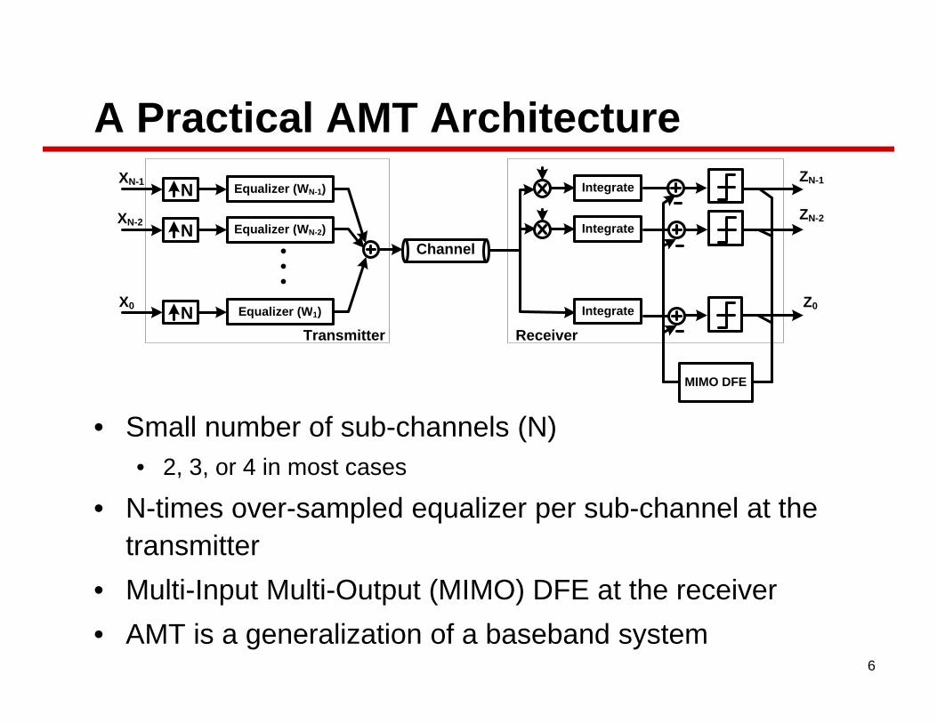
Multi-Tone OperationpTx
Rx
Multi-Drop ConfigurationCi = 1pF
Frequency Response
-20
-10
0
-40
-30
20
dB
Measured
18
0 2 4 6 8 10-50
Frequency (GHz)
Measured3-Channel AMT, 9Gb/s

Multi-PAM Operationp
+3
2PAM/4PAM symbols
+1
-1
-3
+1
-1
+1
-12
Y X 2XY X1 2X2= +
Y(4PAM)
(4PAM) (2PAM) (2PAM)
w0 w1 w2 w3( )
w0 w1 w2 w3X1(2PAM)
2w0 2w1 2w2 2w3X2(2PAM)
19
2w0 2w1 2w2 2w3
Tx configuration in8PAM/16PAM mode

Fractional Equalizationq
Measured
20
Measured8PAM Baseband, 18Gb/s

Cyclically Time-Variant Equalizationy y q
Equalizer
3GHz - I
EqualizerPhase 1
EqualizerPhase 3
6GS/sDAC
6GHz
13GHz - Q
1
0
EqualizerPhase 2
EqualizerPhase 4
6GS/sDAC
0
3GHz Q
1
0
Time-Invariant Time-Variant 4 different
Phase 4
12GS/s DAC
Time Invariant EqualizationSIDR = 26dB
28Gb/s
e a a tEqualizationSIDR = 31dB
28Gb/s
4 different paths to output
4 different responses
21A. Amirkhany, et al, “Time-Variant Characterization and Compensation of Wideband
Circuits,” CICC 2007

Conclusions• A 4-way parallelized equalizer with each parallel
branch programmed independently supports• Analog Multi-Tone
• Multi-level baseband
• Fractional (over-sampled equalization)( p q )
• Cyclically time-variant equalization
• Power overhead due to digital implementation• Power overhead due to digital implementation• Instead of pseudo-DAC
22
• Area overhead for storing more tap coefficients

Digital Implementation Overheadg pAdd four 8-bit
numbers8-bit 2:1 MUX
A 4-tap8-bit
AdderCompressor+ w
- w 4x8
To 7-bit DACA 4 tap 2PAM 6Gbps
Tx
4
Tx
Power 0.5mW10.3 mW
Includes clock power inside flops
5.0 mW
Area 960 um2 16,000 um2 8,000 um2
Total Power Overhead = 16.0 mW (2.6mW/Gbps)
23
Total Area Overhead = 25,000um2
Compared to a Pseudo-DAC implementation


![OpenGL 4.3 API Reference Card Page 1 · OpenGL 4.3 API Reference Card Page 1 OpenGL Operation Floating-Point Numbers [2.3.3] 16-Bit 1-bit sign, 5-bit exponent, 10-bit mantissa Unsigned](https://static.fdocuments.us/doc/165x107/601446bff9d8373bea23177c/opengl-43-api-reference-card-page-1-opengl-43-api-reference-card-page-1-opengl.jpg)