A 1.78–3.05 GHz fractional-N frequency synthesizer with power reduced multi-modulus divider
13
A 1.78–3.05 GHz fractional-N frequency synthesizer with power reduced multi-modulus divider Fuqing Huang • Jianhui Wu • Xincun Ji • Zixuan Wang • Meng Zhang Received: 1 July 2011 / Revised: 26 December 2011 / Accepted: 7 February 2012 / Published online: 22 February 2012 Ó Springer Science+Business Media, LLC 2012 Abstract Nowadays, multi-band frequency synthesizers are very popular for their compatibility, which lowers the chip cost. In this article, a low power 2.4 GHz broadband fractional-N frequency synthesizer based on R–D modula- tion is presented. A novel power reduced multi-modulus divider based on 2/3 divider cells is presented. The ‘‘mod’’ signals are employed to dynamically control the current of the end-of-cycle logic blocks in 2/3 divider cells. When the end-of-cycle logic blocks have no contribution to the divider operation, they are turned off to save power. The saved power is more than 30% in the desired division ratio range. A dual-band voltage controlled oscillator with switched capacitor arrays is designed to cover a wide tuning range. Other circuits such as phase frequency detector, charge pump and loop filter are also integrated on the chip. The whole frequency synthesizer has been fabricated in Chartered 0.18 lm RF CMOS process. Tested results show it covers the tuning range from 1.78 to 3.05 GHz, with phase noise smaller than -85 dBc/Hz at 100 kHz offset, and smaller than -115 dBc/Hz at 3 MHz offset. Its power consumption is only 9.2 mW under 1.8 V supply voltage, and the chip occupies an area of 1.2 mm 9 1.3 mm. Keywords Broadband fractional-N frequency synthesizer R–D modulation Low power multi-modulus divider Wideband voltage controlled oscillator 1 Introduction Frequency synthesizers have been widely used in modern electronic systems for clock and local signal generation. In transceivers, frequency synthesizers are employed to pro- vide local signals for up-conversion and down-conversion mixers. Their tuning range directly determines the receivable signal range of the transceivers, and their performance is very critical for the whole system. Recently, many wireless standards around 2.4 GHz have emerged, such as WLAN, DECT, WCDMA, Bluetooth and Zigbee. Multiband trans- ceivers are very popular for their compatibility, thus lower- ing the chip cost. As main blocks in these transceivers, broadband frequency synthesizers are very desirable [1–4]. The architecture of the frequency synthesizer is very critical for its performance. It can be typically categorized into Integer-N and fractional-N type. Integer-N frequency synthesizers have fundamental tradeoffs between loop bandwidth and channel spacing. While fractional-N fre- quency synthesizers can offer wide bandwidth with narrow channel spacing, because its frequency resolution can be a fraction of the reference frequency [5]. As the loop settling time is inversely proportional to the loop bandwidth, the fractional-N frequency synthesizer is suitable for fast switching applications. Furthermore, the fractional-N fre- quency synthesizer alleviates phase-locked loop (PLL) design constraints for phase noise and reference spurs, because it can use a higher reference frequency than its integer counterpart, which results in lower in-band noise gain and better suppression of reference spurs [6]. Origi- nally, the frequency synthesizer achieves a fractional division ratio by periodically changing its integer division ratio, while its average value is the desired fractional division ratio. This introduces strong fractional spurs. R–D modulator (SDM) is widely used to randomize the division F. Huang (&) J. Wu X. Ji Z. Wang M. Zhang National ASIC System Engineering Research Center, Southeast University, Nanjing 210096, China e-mail: [email protected] 123 Analog Integr Circ Sig Process (2012) 72:97–109 DOI 10.1007/s10470-012-9842-7
Transcript of A 1.78–3.05 GHz fractional-N frequency synthesizer with power reduced multi-modulus divider
A 1.78–3.05 GHz fractional-N frequency synthesizer with powerreduced multi-modulus divider
Fuqing Huang • Jianhui Wu • Xincun Ji •
Zixuan Wang • Meng Zhang
Received: 1 July 2011 / Revised: 26 December 2011 / Accepted: 7 February 2012 / Published online: 22 February 2012
� Springer Science+Business Media, LLC 2012
Abstract Nowadays, multi-band frequency synthesizers
are very popular for their compatibility, which lowers the
chip cost. In this article, a low power 2.4 GHz broadband
fractional-N frequency synthesizer based on R–D modula-
tion is presented. A novel power reduced multi-modulus
divider based on 2/3 divider cells is presented. The ‘‘mod’’
signals are employed to dynamically control the current of
the end-of-cycle logic blocks in 2/3 divider cells. When the
end-of-cycle logic blocks have no contribution to the divider
operation, they are turned off to save power. The saved
power is more than 30% in the desired division ratio range. A
dual-band voltage controlled oscillator with switched
capacitor arrays is designed to cover a wide tuning range.
Other circuits such as phase frequency detector, charge pump
and loop filter are also integrated on the chip. The whole
frequency synthesizer has been fabricated in Chartered
0.18 lm RF CMOS process. Tested results show it covers the
tuning range from 1.78 to 3.05 GHz, with phase noise
smaller than -85 dBc/Hz at 100 kHz offset, and smaller than
-115 dBc/Hz at 3 MHz offset. Its power consumption is
only 9.2 mW under 1.8 V supply voltage, and the chip
occupies an area of 1.2 mm 9 1.3 mm.
Keywords Broadband fractional-N frequency
synthesizer � R–D modulation � Low power multi-modulus
divider � Wideband voltage controlled oscillator
1 Introduction
Frequency synthesizers have been widely used in modern
electronic systems for clock and local signal generation. In
transceivers, frequency synthesizers are employed to pro-
vide local signals for up-conversion and down-conversion
mixers. Their tuning range directly determines the receivable
signal range of the transceivers, and their performance is
very critical for the whole system. Recently, many wireless
standards around 2.4 GHz have emerged, such as WLAN,
DECT, WCDMA, Bluetooth and Zigbee. Multiband trans-
ceivers are very popular for their compatibility, thus lower-
ing the chip cost. As main blocks in these transceivers,
broadband frequency synthesizers are very desirable [1–4].
The architecture of the frequency synthesizer is very
critical for its performance. It can be typically categorized
into Integer-N and fractional-N type. Integer-N frequency
synthesizers have fundamental tradeoffs between loop
bandwidth and channel spacing. While fractional-N fre-
quency synthesizers can offer wide bandwidth with narrow
channel spacing, because its frequency resolution can be a
fraction of the reference frequency [5]. As the loop settling
time is inversely proportional to the loop bandwidth, the
fractional-N frequency synthesizer is suitable for fast
switching applications. Furthermore, the fractional-N fre-
quency synthesizer alleviates phase-locked loop (PLL)
design constraints for phase noise and reference spurs,
because it can use a higher reference frequency than its
integer counterpart, which results in lower in-band noise
gain and better suppression of reference spurs [6]. Origi-
nally, the frequency synthesizer achieves a fractional
division ratio by periodically changing its integer division
ratio, while its average value is the desired fractional
division ratio. This introduces strong fractional spurs. R–Dmodulator (SDM) is widely used to randomize the division
F. Huang (&) � J. Wu � X. Ji � Z. Wang � M. Zhang
National ASIC System Engineering Research Center,
Southeast University, Nanjing 210096, China
e-mail: [email protected]
123
Analog Integr Circ Sig Process (2012) 72:97–109
DOI 10.1007/s10470-012-9842-7

ratio for mitigating fractional spurs. The remaining quan-
tization noise is shifted to high frequency and can be
suppressed by the loop low pass characteristic [6, 7].
Low power design is a very hot topic in electronic
systems, especially in handset devices. In RF frequency
synthesizers, the multi-modulus dividers work at the
highest frequency and are constructed by complex logic
circuits, so they usually consume most of the power [8]. A
low power multi-modulus divider is very critical to lower
the overall power consumption of a RF frequency synthe-
sizer. A novel power reduced multi-modulus divider based
on 2/3 divider cells is presented. The ‘‘mod’’ signals are
employed to dynamically control the current of the end-of-
cycle logic blocks in 2/3 divider cells to save power. The
voltage controlled oscillator (VCO) is another power
hungry component in the RF frequency synthesizer. For
wideband VCO, the quality factor (Q) of the switched
capacitor array may be comparable to that of the inductor,
which may deteriorate the startup margin, the power dis-
sipation and the phase noise performance. Moreover, the
VCO tuning gain may vary greatly, which is harmful to the
synthesizer stability. A dual-band VCO comprising a high-
frequency band VCO (HB-VCO) and a low-frequency
band VCO (LB-VCO) is employed in the frequency syn-
thesizer to solve these issues.
Based on the low power multi-modulus divider and the
dual-band VCO, a low power broadband frequency syn-
thesizer centered at 2.4 GHz is presented in this article.
Design details of main building blocks are described. The
whole frequency synthesizer has been fabricated in Char-
tered 0.18 lm RF CMOS process. Measured results show
the whole synthesizer covers the tuning range from
1.78 GHz to 3.05 GHz, while consuming only 9.2 mW
under 1.8 V supply voltage. The measured phase noise is
smaller than -85 dBc/Hz at 100 kHz offset, and smaller
than -115 dBc/Hz at 3 MHz offset. This paper is orga-
nized as follow. In Sect. 2, the whole fractional-N fre-
quency synthesizer architecture is described. In Sect. 3,
design details of individual blocks are presented. Then,
experimental results are given in Sect. 4, followed by the
conclusion in Sect. 5.
2 Fractional-N frequency synthesizer architecture
The block diagram of the whole frequency synthesizer is
depicted in Fig. 1. It is a type II fourth order PLL based
frequency synthesizer. The phase domain model of the fre-
quency synthesizer is depicted in Fig. 2. The loop bandwidth
xc of the frequency synthesizer can be expressed as,
xc ¼IcpKvcoR1
N� C1
C1 þ C2 þ C3
ð1Þ
where Icp is the charge pump (CP) current, Kvco is the VCO
tuning gain, N is the division ratio, R1, R3, C1, C2 and C3
are the component parameters of the low pass filter (LPF).
The VCO tuning gain Kvco may change greatly in a wide
output frequency range. To cover a wide tuning range
without a large Kvco variation, the VCO is composed of a
HB-VCO and a LB-VCO. Each of them employs a 4 bit
switched capacitor array for coarse tuning and a couple of
accumulation-mode MOS (AMOS) varactors for fine tun-
ing. As described in Sect. 1, the dual-band VCO is also
benefit for improving the Q of the LC-tank, which is
desirable for low power design. The CP current is made
programmable to compensate for the Kvco variation.
An external 40 MHz XTAL is adopted for reference. A
sequential phase frequency detector (PFD) is employed to
detect the phase and the frequency errors between the ref-
erence signal Fref and the VCO divided signal Fdiv. The 3rd
order passive LPF is employed to smooth the CP output
current and convert it to voltage for controlling the VCO. The
multi-modulus divider is composed of 6 cascaded 2/3 divider
cells, which is improved from the divider reported in [9].
It covers the division ratio range from 32 to 127, which
is sufficient for the system. A 20 bit 3rd order MASH 1-1-1
R–D modulator is used to modulate the integer division ratio
for getting a frequency step of 40/220 MHz.
The transfer function Zlpf(s) of the 3rd order loop filter
can be expressed as follow.
ZlpfðsÞ ¼1
s C1 þ C2 þ C3ð Þ� 1þ sR1C1
1þ s R1C1 C2þC3ð ÞþR3C3 C1þC2ð ÞC1þC2þC3
þ s2 R1R3C1C2C3
C1þC2þC3
ð2Þ
Then the open loop transfer function Hol(s) of the
frequency synthesizer can be derived as,
HolðsÞ ¼Icp
2p� ZlpfðsÞ �
2pKvco
Ns
¼ Icp � Kvco
s2NðC1 þ C2 þ C3Þ
� 1þ sR1C1
1þ s R1C1 C2þC3ð ÞþR3C3 C1þC2ð ÞC1þC2þC3
þ s2 R1R3C1C2C3
C1þC2þC3
ð3Þ
So the closed loop transfer function from the input phase
ain(s) to the output phase aout(s) can be given as follow.
HinðsÞ ¼/outðsÞ/inðsÞ
¼ N � HolðsÞ1þ HolðsÞ
¼N x� xcð ÞN � HolðsÞ x� xcð Þ
(ð4Þ
And the closed loop transfer function from the input
phase avco(s) to the output phase aout(s) can be expressed
as,
98 Analog Integr Circ Sig Process (2012) 72:97–109
123

HvcoðsÞ ¼/outðsÞ/vcoðsÞ
¼ 1
1þ HolðsÞ
¼1
HolðsÞx� xcð Þ
1 x� xcð Þ
8<: ð5Þ
The closed loop transfer function from the input voltage
�vlpf(s) to the output phase aout(s) can be given as,
HlpfðsÞ ¼/outðsÞvlpfðsÞ
¼ 2pKvco
s� 1
1þ HolðsÞ
¼
2pKvco
s � HolðsÞx� xcð Þ
2pKvco
sx� xcð Þ
8>><>>: ð6Þ
The noise from XTAL, PFD, CP, Multi-Modulus Divider
and R–D Modulator can be equivalent to an input phase noise
ain,n(s). According to Eq. 4, this noise is low pass filtered by
the PLL loop, when it is transferred to the synthesizer output.
The phase noise from the VCO is high pass filtered referring
to Eq. 5. Meanwhile, the output equivalent voltage noise �vlpf
of the LPF is band pass filtered by the loop characteristic. The
corner frequencies of the three transfer functions Hin(s),
Hvco(s) and Hlpf(s) are about the loop bandwidth xc. So the
loop bandwidth is very important for the phase noise
performance of the frequency synthesizer. The wider the
loop bandwidth, the more the phase noise from the VCO will
be suppressed. And the narrower the loop bandwidth, the
more the noise from XTAL, PFD, CP, multi-modulus divider
and R–D modulator will be filtered. Meanwhile, the loop
settling time is inversely proportional to the loop bandwidth.
Thus, the selection of the loop bandwidth is a trade-off.
3 Building blocks
3.1 PFD and CP
The PFD is shown in Fig. 3. It adopts RS flip-flops to
perform phase and frequency comparison. A ‘‘delay’’ cell
is inserted to eliminate the dead zone problem, which is
important for the PFD and CP linearity. However, a large
delay will cause the ‘‘up’’ and ‘‘dn’’ signals both high for
long time when the PLL is locked, which is undesirable for
noise and spur performance. An optimized value is
obtained from simulation. Two single end signal to dif-
ferential signal converters (S2D) are adopted to control the
current steering CP. The output inverters are constructed in
positive feedback structures to shorten the output signals’
transition time and improve their symmetry.
PFD CP VCO
Multi-ModulusDivider
MASH 1-1-1(20 bit)
FractionalDivider
D <6:0>
Frefupp
dnn
vctrl
Fout
+SDM<2:0>
F<19:0> N<6:0>
Fdiv
sdm_clk
R1R3
C1
C2 C3
LPFupn
dnp
Fig. 1 Block diagram of the
whole frequency synthesizer
Fig. 2 Phase domain model of
the frequency synthesizer
Analog Integr Circ Sig Process (2012) 72:97–109 99
123

The CP comprises three blocks: a low voltage cascode
bias block, a programmable current array and a current
switching block, as depicted in Fig. 4. The bias block uses
low voltage cascode current mirrors to enlarge the output
voltage range. To reduce the variation of the PLL loop
bandwidth, a programmable current array is employed. It
comprises four individual current sources which can be
switched on or off, respectively. This makes 16 kinds of
current values ranging from 20 to 320 lA available. The
current step is 20 lA. In the current switching block, NM1
and PM1 compose a complementary transmission gate,
rejecting clock feed-through and charge injection. They
together with NM2 and PM2 form a differential current
switch. A rail-to-rail amplifier is employed to make the
voltage on the node X consistent with the voltage on the
node Y, which mitigates the charge sharing effect.
Fref
Fdiv
up
dn
delay
upp
upn
dnp
dnn
Single end signal to differential signal converter (S2D)
Fig. 3 Logic diagram of the PFD
Fig. 4 Schematic of the CP
100 Analog Integr Circ Sig Process (2012) 72:97–109
123
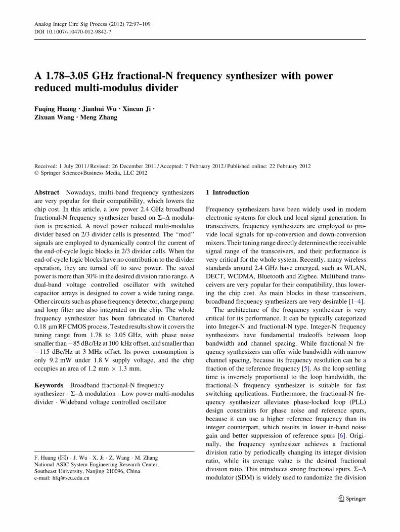
3.2 VCO
To cover a wide output frequency range without deterio-
rating the phase noise and the spur performance of the
frequency synthesizer, the VCO is constructed by a HB-
VCO and a LB-VCO. They employ the same topology.
Schematic of a single VCO is depicted in Fig. 5. It employs
the complementary cross-coupled topology to improve
power efficiency. PMOS is used for the tail current source,
because PMOS has low flicker noise and good isolation
from substrate noise [10]. The bias current is made pro-
grammable to mitigate the output amplitude variation [11].
PM5 is used as a capacitor, together with R1 forming a LPF
to suppress the noise from the bias circuit. The cross
coupled PMOS pair (PM1, PM2) and the cross coupled
NMOS pair (NM1, NM2) are adopted to compensate
energy loss in the LC-tank for reliable oscillation. The
negative resistance of the PMOS cross coupled pair is
made equal to that of the NMOS cross coupled pair for
good output waveform symmetry, thus lowering the flicker
noise up-conversion effect [12]. L is a spiral inductor with
Q from 7 to 8.5 for both the HB-VCO and the LB-VCO in
their output frequency range. AMOS varactors are used for
fine tuning. A 4 bit switched capacitor array is employed to
extend the output frequency range of a single VCO. The
highest control bit (S4) is used to control which VCO is in
active. The tank including the switched capacitor array is
optimized to maximize its loaded Q, and the tail current is
biased to make the VCO work at the edge of the voltage
limited region and the current limited region, thus saving
power to achieve good phase noise performance [12].
3.3 Multi-modulus divider and SDM
The truly modular multi-modulus divider based on 2/3
divider cells is very popular for its low power dissipation,
high design flexibility and high reusability [9, 13–15].
Figure 6 shows its diagram. Generally, the current of each
2/3 cell is scaled down with its downscaled working fre-
quency to optimize power consumption. Detailed analysis
of one 2/3 cell shows the power consumption can be
Vdd S0
S2
S3
CC
4C4C
8C8C
Vctrl
R1
PM5
PM6 PM4
NM1 NM2
PM1 PM2
NM3
NM5
NM6
L
Cf Cf
Cv Cv
S4 PM3S1
2C2CNM4L
Programmablecurrent array
Fig. 5 Schematic of a single VCO
2/3 cell1
fo1
mod1
fin
…
P0 P1 Pn-2
MiMo
FoFi
2/3 cell2
MiMo
FoFi
2/3 celln-1
MiMo
FoFifo2
mod2
fon-1
modn-1
2/3 celln
MiMo
FoFifon
Pn-1
Fig. 6 Truly modular multi-modulus divider reported in [9]
Analog Integr Circ Sig Process (2012) 72:97–109 101
123

lowered greatly by dynamically controlling the current of
its end-of-cycle logic block.
3.4 Detailed analysis of the 2/3 divider cell
The 2/3 divider cell proposed in [13] is suitable for high
speed operation, as depicted in Fig. 7. It comprises two
functional blocks: the prescaler logic block and the end-of-
cycle logic block. The prescaler logic block divides the Fi
input signal either by 2 or 3 upon control of the end-of-
cycle logic block. The end-of-cycle logic block determines
the momentaneous division ratio of the cell, based on the
state of the Mi and P signals. Only when Mi signal
becomes active (once in a whole division cycle), is the state
of P input checked to determine whether the prescaler
swallows one extra period of its input signal or not, and if
P = 1, the prescaler logic block performs a divide-by-3
operation, otherwise it still divides by 2. So the end-of-
cycle logic block can be turned off when its corresponding
Mi signal is inactive to lower power consumption.
The Mi signal is fed back from the next 2/3 cell, and its
high-level duration is equal to one long output period of its
corresponding 2/3 cell. Here, the long period refers to the
period when the corresponding 2/3 cell can swallow its
input signal. Therefore, the current of latch3 and latch4 is
only needed in one long Fo signal period for correct
operation, and the saved power is relative to the long
period of Fo signal. In a chain of cascaded 2/3 divider cells,
the first few stages consume most of the power and their
corresponding long period of Fo signal is very small with
respect to the whole division cycle. So the end-of-cycle
logic blocks can be turned off most of the time in every
division cycle, thus saving much power.
Source coupled logic (SCL) is usually used in the design
of dividers for its high speed operation, low switching
d qlatch1
clk qn
d qlatch2
clk qn
q dlatch4
qn clk
q dlatch3
qn clk
Fi
Fo
Mi
Mo
P
prescaler logic
end-of-cycle logic
Fig. 7 Logic diagram of 2/3 divider cell.3.3.2 Improved 2/3 Divider
Cell
clk
vb
Vdd
2/3 cell
MiMo
FoFi Lp
Lc
a q
b
AND_latch1
clk q
d q
latch2
clk
q a
b
AND_latch3
Lc Lp clkq
qFiMo
Mi
Fo
PLc Lp
Vdd
LpLpLp
clk
clk clk
d d
a
b
a
b
LcLc
q a
b
AND_latch4
Lc Lp clkq
MNMMPMVdd
LpLpLp
clkclk
a
b
a
b
LcLc
MNPMPP
vb
Vdd
clk clk
a
b
a
b
vbe vbe
q3
Fig. 8 Improved 2/3 divider cell
102 Analog Integr Circ Sig Process (2012) 72:97–109
123

noise and good EMC properties [8, 9]. The AND gate is
usually embedded in the latch to improve working speed,
so is called AND_latch. To realize the idea of power
reduction with low hardware complexity, the conventional
2/3 divider cell is improved. As shown in Fig. 8,
AND_latch1 and latch2 are implemented in conventional
SCL structure with PMOS active resistors as load, while
AND_latch3 and AND_latch4 are improved SCL struc-
tures with shut-down mode. When Lc, Lp = 11, the end-
of-cycle logic block works in the turn-on mode and its
corresponding 2/3 cell acts as a conventional one. And
when Lc, Lp = 00, the current of the end-of-cycle logic
block is turned off and it works in the shut-down mode.
PMOS MPP and MPM are used to set q of AND_latch3
and AND_latch4 high, ensuring correct divide-by-2 oper-
ation of the 2/3 cell. NMOS MNP and MNM are employed
to clamp the voltages of q3 and Mo, which is benefit for
high speed operation. The state Lc, Lp = 10 is a transition
state, and the state Lc, Lp = 01 is forbidden. Voltages vb
and vbe are respective biases for the prescaler logic block
and the end-of-cycle logic block.
The transition between the shut-down mode and the
turn-on mode is critical for correct operation. Some timing
(b)
Lc
Lp
Mi active inactive
one division cycle
1ττ τ
τ2 3
4
(a)
Fig. 9 a Timing diagram of the mode control signals. b Transient
response of a 2/3 cell under mode transition
fin
P0 P1
2/3 cell2 SCL
MiMo
FoFi Lp
Lc
fo2
mod2
2/3 cell1 SCL
MiMo
FoFi Lp
Lc
fo1
mod1
2/3 cellTSPC
4mod4
fo4
P3
2/3 cellTSPC
3
fo3
mod3
re2/3 cellTSPC
6 mod6
fo6
2/3 cellTSPC
5
fo5
mod5
P4 P5
D QlatchTSPCC QN
0
1D Q
dffTSPC
C QN
P6
P6
fo2 Fout
P2
(a)
fin
P0 P1
2/3 cell2 SCL
MiMo
FoFifo2
mod2
2/3 cell1 SCL
MiMo
FoFifo1
mod1
2/3 cellTSPC
4mod4
fo4
P3
2/3 cellTSPC
3
fo3
mod3
re2/3 cellTSPC
6 mod6
fo6
2/3 cellTSPC
5
fo5
mod5
P4 P5
D QlatchTSPCC QN
0
1D Q
dffTSPC
C QN
P6
P6
fo2 Fout
P2
(b)
Fig. 10 a Block diagram of proposed divider. b Block diagram of the conventional divider
Analog Integr Circ Sig Process (2012) 72:97–109 103
123

constraints should be satisfied among the mode control
signals Mi, Lp and Lc. As depicted in Fig. 9(a), the time
durations s1 and s4 are necessary to turn on the tail current
before Lp is set to low, avoiding metastabilities of q3 and
Mo when the end-of-cycle logic block switches between
the shut-down mode and the turn-on mode. The time
durations s2 and s3 are used to turn off MPP and MPM
properly before or after Mi signal becoming active. Fig-
ure 9(b) shows transistor level simulation waveforms of a
2/3 cell under mode transition. It can see the total current
Itotal in the turn-on mode is about twice as much as that in
the shut-down mode.
3.4.1 Proposed multi-modulus divider
Based on the behavioral simulation of several cascaded 2/3
divider cells in [13], the ‘‘mod’’ signals (mod1,…,
modm,…,modn-1) can be employed to dynamically control
the current of the end-of-cycle logic blocks in 2/3 divider
cells, e.g. modm?2 and modm?1 signals can be used as Lc and
Lp signals directly for the m-th 2/3 divider cell to switch the
mode of the end-of-cycle logic block. This greatly simplifies
hardware complexity. The multi-modulus divider adopting
the above mentioned power reduction technique is shown in
Fig. 10(a). The first two 2/3 cells are implemented with the
improved 2/3 divider cell for low power consideration,
which still retains the high speed property of the SCL
structure. The other 2/3 cells, latches and flip-flops are all
constructed by true single phase clock (TSPC) logic. They
can work under the reduced working frequency only with
dynamic power consumption. When working in the frac-
tional mode (the division ratio is fraction), the divider may
switch between 5-cell and 6-cell configuration. To make the
divider support seamless switching between 5-cell and 6-cell
mode, some additional logic circuits are added [14]. The
division ratio range is from 32 to 127. And the division ratio
(DR) can be expressed as follow.
DR ¼ P6 � 26 þ P5 � P6 þ P6
� �� 25 þ P4 � 24 þ P3 � 23
þ P2 � 22 þ P1 � 21 þ P0 � 20 ð7Þ
Fig. 11 a Saved power against
division ratio in theory. b Saved
power against division ratio in
practice
Fig. 12 Z domain model of MASH 1-1-1 modulator
Fig. 13 Microphotograph of the frequency synthesizer prototype
chip
104 Analog Integr Circ Sig Process (2012) 72:97–109
123

A comparison has been done between the proposed divider
and the conventional one. The conventional divider is
different from the proposed one only by adopting con-
ventional SCL 2/3 cells in the first two stages, as shown in
Fig. 10(b). Current of each SCL 2/3 cell is usually scaled
down to half of its front one to optimize power dissipation
[9]. Let’s assume the first 2/3 cell in Fig. 10(b) dissipates a
current of Itail, e.g. each latch or AND_latch of it consumes
Itail/4, so the second 2/3 cell dissipates a total current of
Itail/2. If we omit dynamic power dissipation and turn off
the end-of-cycle logic blocks in the two SCL 2/3 cells all
the time, then the saved power percentage will be 50%. In
every division cycle, however, the end-of-cycle logic block
of the m-th 2/3 cell in Fig. 10(a) needs to be active for
about one long output period of the m ? 2-th 2/3 cell,
where m is smaller than 2. For example, the end-of-cycle
logic block of the first 2/3 cell in Fig. 10(a) needs to be
active for (23 ? 22•P2 ? 2•P1 ? P0)•Tin, where Tin is the
input signal period. Fortunately, most power is consumed
by the first two stages, and the active time of their end-of-
cycle logic blocks is much less than the whole division
cycle. So the saved power can be large. The saved power
by using the proposed divider can be analyzed as follow.
First, the power dissipated in every division cycle by the
prescaler logic blocks and the end-of-cycle logic blocks of
the two SCL 2/3 cells in Fig. 10(a) can be calculated. The
results are listed below.
1st : Pe 1 ¼ItailVddTin
223 þ 22P2 þ 21P1 þ P0
� �ð8Þ
Pp 1 ¼ItailVddTin
2
hP6 � 26 þ P5 � P6 þ P6
� �� 25
þ P4 � 24 þ P3 � 23 þ P2 � 22 þ P1 � 21 þ P0 � 20ið9Þ
2nd: Pe 2 ¼ItailVddTin
2224 þ 23P3 þ 22P2 þ 21P1 þ P0
� �ð10Þ
Pp 2 ¼ItailVddTin
22
�P6 � 26 þ P5 � P6 þ P6
� �� 25
þ P4 � 24 þ P3 � 23 þ P2 � 22 þ P1 � 21 þ P0 � 20�ð11Þ
where Pe_1 and Pp_1 are the power consumed by the end-
of-cycle logic block and the prescaler logic block of the
first 2/3 cell. Pe_2 and Pp_2 are the power consumed by the
end-of-cycle logic block and the prescaler logic block of
the second 2/3 divider cell.
Secondly, the total power consumed by the two SCL 2/3
cells with the power reduction technique is,
Pscl w ¼Pe 1þPe 2þPp 1þPp 2
¼ 3ItailVddTin
4
�P6�26þ P5�P6þP6
� ��25
þP4�24þP3�23þP2�22þP1�21þP0�20�
þ ItailVddTin 8þ2P3þ3P2þ3
2P1þ
3
4P0
� �
¼ ItailVddTin
h48P6þ24 P5�P6þP6
� �þ12P4
þ8P3þ6P2þ 3P1þ3
2P0þ8
ið12Þ
Thirdly, the total power consumed by the two SCL 2/3
cells without the power reduction technique can be
expressed as,
Pscl wo¼ 2 Pp 1þPp 2
� �¼ 3ItailVddTin
2
hP6�26þ P5�P6þP6
� ��25
þP4�24þP3�23þP2�22þP1�21þP0�20�
¼ ItailVddTin
h96P6þ48 P5�P6þP6
� �þ24P4
þ12P3þ6P2þ3P1þ3
2P0
ið13Þ
Let’s assume the power dissipated by other dynamic cir-
cuits in every division cycle is Pdynamic = ratio*Pscl_wo,
the saved power can be got as follow.
Simulation shows the ratio between Pdynamic and Pscl_wo
is smaller than 10%. The saved power is between 25 and
45% according to Eq. 14, as depicted in Fig. 11(a).
Figure 11(b) shows the saved power by using the pro-
posed divider is more than 30% in practice. The small
discrepancies between Figs. 11(a) and (b) are due to the
variation of the dynamic power against division ratio
and the smaller turn-on time of the end-of-cycle logic
saved power ¼ 1� Pscl w þ Pdynamic
Pscl wo þ Pdynamic
¼ 1�ItailVddTin 48P6 þ 24 P5 � P6 þ P6
� �þ 12P4 þ 8P3 þ 6P2 þ 3P1 þ 3
2P0 þ 8
� �þ Pdynamic
ItailVddTin 96P6 þ 48 P5 � P6 þ P6
� �þ 24P4 þ 12P3 þ 6P2 þ 3P1 þ 3
2P0
� �þ Pdynamic
ð14Þ
Analog Integr Circ Sig Process (2012) 72:97–109 105
123

blocks in practice. The current of the end-of-cycle logic
blocks cannot be turned on immediately in reality. Most
of the power is consumed by the two SCL 2/3 cells in
the two dividers. The larger the division ratio, the
smaller will be the turn-on time of the end-of-cycle logic
blocks with respect to the whole division cycle. The
saved power can approach 50% with larger division
ratio.
3.4.2 R–D modulator
A 20 bit 3rd order MASH 1-1-1 R–D modulator is used to
modulate the integer division ratio for getting a very small
frequency step [16]. Furthermore, an odd initial value is set
to the first accumulator in the modulator to randomize its
output bit pattern. Figure 12 shows its z domain model. Its
transfer function can be expressed as,
Fig. 14 a Measured VCO tuning curves, b output spectrum and phase noise of the frequency synthesizer at 2.4 GHz, c output spectrum and
phase noise of the frequency synthesizer at 2.42 GHz
106 Analog Integr Circ Sig Process (2012) 72:97–109
123

YðzÞ ¼ XðzÞ þ 1� z�1� �3�E3ðzÞ ð15Þ
3.5 LPF and other circuits
To suppress the quantization noise of the 3rd order R–Dmodulator and reference spurs. A 3rd order RC LPF is
employed as the loop filter. The loop bandwidth of the
frequency synthesizer is designed to be about 350 kHz.
The component parameters of the loop filter are
R1 = 19.5 kX, R3 = 19.8 kX, C1 = 85 pF, C2 = 4.25 pF
and C3 = 1 pF. Assistant circuits such as the band-gap
reference and the I2C are all integrated on the chip.
4 Experimental results
The whole frequency synthesizer has been fabricated in
Chartered 0.18 lm RF CMOS process. Low speed digital
circuits, such as SDM and I2C, are synthesized by design
compiler, and the layouts of them are realized by Astro.
Other circuits are full-custom designed. Figure 13 shows
its microphotograph. The whole chip occupies an area of
1.2 mm 9 1.3 mm.
The circuit is tested from a 1.8 V supply voltage. Measured
VCO tuning curves are shown in Fig. 14(a). The LB-VCO
covers the output frequency range from 1.78 to 2.438 GHz,
and the HB-VCO covers the output frequency range from
2.375 to 3.05 GHz. The output spectrum and phase noise of
the frequency synthesizer at 2.4 GHz (corresponding to
integer division ratio of 60) and 2.42 GHz (corresponding to
fractional division ratio of 60.5) are shown in Fig. 14(b) and
(c). Figure 15 depicts the measured phase noise against the
output frequency of the frequency synthesizer. The in-band
phase noise in the integer mode (when the division ratio is
integer) is better than that in the fractional mode (when the
division ratio is fraction), because the nonlinearity of
the PFD&CP folds the high frequency quantization noise of
the SDM into in-band when the frequency synthesizer works
in the fractional mode. Meanwhile, the out-of-band phase
noise of the integer mode also outperforms that of the frac-
tional mode because of the wide loop bandwidth. The phase
noise in the fractional mode can be improved by further
enhancing the linearity of the PFD and CP and by setting the
loop bandwidth narrower or by adopting a compensation
technique with digital-to-analog converter and so on [17].
These will be our future research focus. The measured phase
noise of the whole frequency synthesizer is smaller than -85
dBc/Hz at 100 kHz offset, and smaller than -115 dBc/Hz at
3 MHz offset. It dissipates about 5.1 mA at total. Of which,
the divider consumes 4.1 mW. The VCO dissipates 3.6 mW,
and the PFD&CP uses about 0.9 mW. The SDM and I2C draw
another 0.6 mW.
Table 1 shows the performance summary of the fre-
quency synthesizer and the comparison with some
Fig. 15 Measured output phase noise against output frequency
Table 1 Performance summary and comparison
Work [1] [4] [15] [17] [18] [19] [20] This work
Performance
CMOS process (lm) 0.25 0.13 0.18 0.18 0.18 0.13 0.065 0.18
Supply voltage (V) 2.5 1.2 2 1.8 1 1.5 1.2 1.8
Reference frequency (MHz) 13.3 20 10 14.33 11 50 40 40
Tuning range (GHz) 3.2–4 3.8–5.5 2.5–3.2 1.6–2.0 5.45–5.65 3.2–4.2 3.0–3.6 1.78–3.05
phase Noise (dBc/Hz) \-105 -72 \-66 -108 \-85
@10 kHz @100 kHz \-122 -98 @92 kHz @400 kHz -104 @100 kHz
\-136 -121 @1 MHz @in-band \-136 -150 @400 kHz \-115
@20 MHz @5 MHz @20 MHz @20 MHz @3 MHz
Reference spurs (dBc) -64 \-55 NA -75 -80 -65 -65 \-51
Chip area (mm2) 1.7 1.3 0.85 2 1.03 0.95 0.4 1.56
Power dissipation (mW) 93 31.2 26.8 29 27.5 39 80 9.2
Analog Integr Circ Sig Process (2012) 72:97–109 107
123

previously published works. It can see that the frequency
synthesizer in this work has great advantages in frequency
coverage and power dissipation with moderate phase noise
performance. The phase noise performance is inferior to
that of [15, 17, 19, 20], because they use additional
quantization noise suppression techniques which increase
power consumption and chip area.
5 Conclusion
A 2.4 GHz broadband fractional-N frequency synthesizer is
developed for multi-standard wireless applications in Char-
tered 0.18 lm RF CMOS process. A dual-band VCO is
designed, achieving the tuning range from 1.78 to 3.05 GHz.
A low power multi-modulus divider suitable for R–D frac-
tional-N frequency synthesizer is proposed. Design details of
main blocks are described. The measured phase noise of the
whole frequency synthesizer is smaller than -85 dBc/Hz at
100 kHz offset, and smaller than -115 dBc/Hz at 3 MHz
offset, while consuming only 9.2 mW under 1.8 V supply
voltage. These make it suitable for low power multi-standard
wireless applications around 2.4 GHz.
Acknowledgment This study was supported in part by the National
Natural Science Foundation of China under no. 60871079.
References
1. Terrovitis, M., Mack, M., Singh, K., and Zargari, M. (2004). A
3.2 to 4 GHz, 0.25 lm CMOS frequency synthesizer for IEEE
802.11a/b/g WLAN. IEEE International Solid-State CircuitsConference, 98–515.
2. Maeda, T. et al. (2004). A direct-conversion CMOS transceiver
for 4.9–5.95 GHz multi-standard WLANs. IEEE InternationalSolid-State Circuits Conference. Digest Of Technical pp. 90–515.
3. Rogers, J. W. M., Dai, F. F., et al. (2005). A multiband DRfractional-N frequency synthesizer for a MIMO WLAN Trans-
ceiver RFIC. IEEE Journal of Solid-State Circuits, 40(3),
678–689.
4. Lee, J. Y., Kim, k., Kwon, J., Lee, S. C., Kim, J., & Lee, S. H.
(2006). A 3.8–5.5-GHz multi-band CMOS frequency synthesizer
for WPAN/WLAN applications. IEEE Custom Integrated Cir-cuits Conference. pp. 377–380.
5. Rhee, W., Song, B. S., & Ali, A. (2000). A 1.1-GHz CMOS
fractional-N frequency synthesizer with a 3-b third-order DRmodulator. IEEE Journal of Solid-State Circuits, 35(10),
1453–1460.
6. Shu, K., & Edgar, S. S. (2005). CMOS PLL synthesizers: Analysisand design. New York: Springer.
7. Riley, T. A. D., Copeland, M. A., & Kwasniewski, T. A. (1993).
Delta-sigma modulation in fractional-N frequency synthesis.
IEEE Journal of Solid-State Circuits, 28(5), 553–559.
8. Nonis, R., Palumbo, E., Palestri, P., & Selmi, L. (2007). A design
methodology for MOS current-mode logic frequency dividers.
IEEE Transactions on Circuits and Systems-I: Regular Papers,54(2), 245–254.
9. Vaucher, C. S., Ferencic, I., Locher, M., Sedvallson, S., Voegeli,
U., & Wang, Z. (2000). A Family of low-power truly modular
programmable dividers in standard 0.35-lm CMOS technology.
IEEE Journal of Solid-State Circuits, 35(7), 1039–1045.
10. Jerng, A., & Sodini, C. G. (2005). The impact of device type and
sizing on phase noise mechanisms. IEEE Journal of Solid-StateCircuits, 40(2), 360–369.
11. Berny, A. D., Niknejad, A. M., & Meyer, R. G. (2005). A 1.8-
GHz LC VCO with 1.3-GHz tuning range and digital amplitude
calibration. IEEE Journal of Solid-State Circuits, 40(4), 909–917.
12. Hajimiri, A., & Lee, T. H. (1998). A general theory of phase
noise in electrical oscillators. IEEE Journal of Solid-State Cir-cuits, 33(2), 179–194.
13. Wafa, A., & Ahmed, A. (2004). High-speed RF multi-modulus
prescaler architecture for R–D fractional-N PLL frequency syn-
thesizers. Proceedings of the IEEE International Symposium onCircuits and Systems. pp. 241–244.
14. Nuzzo1, P., Vengattaramane1, K., Ingels1, M., Giannini1, V.,
Steyaert, M., & Craninckx, J. (2009). A 0.1–5 GHz dual-VCO
software-defined RD frequency synthesizer in 45 nm digital
CMOS. IEEE Radio Frequency Integrated Circuits Symposium.pp. 321–324.
15. Yang, Y. C., & Lu, S. S. (2008). A quantization noise pushing
technique for RD fractional-N frequency synthesizers. IEEETransactions on Microwave Theory and Techniques, 56(4),
817–825.
16. Kozak, M., & Kale, I. (2001). A pipelined noise shaping coder for
fractional-N frequency synthesis. IEEE Transactions on Instru-mentation and Measurement, 50(5), 1154–1161.
17. Gupta, M., & Song, B. S. (2006). A 1.8-GHz spur-cancelled
fractional-N frequency synthesizer with LMS-based DAC gain
calibration. IEEE Journal of Solid-State Circuits, 41(12),
2842–2851.
18. Leung, G. C. T., & Luong, H. C. (2004). A 1-V 5.2-GHz CMOS
synthesizer for WLAN applications. IEEE Journal of Solid-StateCircuits, 39(11), 1873–1882.
19. Hsu, C. M., Straayer, M. Z., & Perrott, M. H. (2008). A low-noise
wide-BW 3.6-GHz digital DR fractional-N frequency synthesizer
with a noise-shaping time-to-digital converter and quantization
noise cancellation. IEEE Journal of Solid-State Circuits, 43(12),
2776–2786.
20. Zanuso, M., Levantino, S., Samori, C., & Lacaita, A. L. (2011). A
wideband 3.6 GHz digital DR fractional-N PLL with phase
interpolation divider and digital spur calculation. IEEE Journal ofSolid-State Circuits, 46(3), 627–638.
Fuqing Huang was born in
Hunan, China, in 1986. He
received the BS degree in elec-
tronic science and technology
from Hunan University, Chang-
sha, China, in 2007 and is cur-
rently working toward the PhD
degree at Southeast University,
Nanjing, China. His research
interests include analog-mixed
integrated circuit and radio-fre-
quency integrated circuit
design, especially in the field of
low power, low phase noise and
fast setting frequency synthe-
sizer design with CMOS technology.
108 Analog Integr Circ Sig Process (2012) 72:97–109
123
Jianhui Wu was born in Anhui,
China, in 1966. He received the
MS, and PhD degrees from
Southeast University, Nanjing,
China, in 1992 and 2000, respec-
tively, both in electronic engineer-
ing. He is currently a Professor in
National ASIC System Engineer-
ing Research Center, Southeast
University, Nanjing, China. His
research interests include RF IC
design and mix-signal IC design.
He is the author or coauthor of
more than 50 papers and the holder
of 20 Chinese patents.
Xincun Ji was born in Jiangsu,
China, in 1983. He received the
BS degree from Suzhou Uni-
versity, Suzhou, China, in 2006
and is now pursuing the PhD
degree in electronics at South-
east University, Nanjing, China.
His research interests include
RF transceivers and phase-
locked loop design.
Zixuan Wang was born in Ji-
angsu, China, in 1982. He received
the BS degree in electronic infor-
mation engineering from Nanjing
Normal University, Nanjing,
China, in 2005. He is currently
working toward the PhD degree at
Southeast University, Nanjing,
China, His research interests
include analog-mixed integrated
circuit and digital integrated cir-
cuit design, especially in the field
of low power and high resolution
all digital PLL design with CMOS
technology.
Meng Zhang was born in
China, in July, 1964 and
received the MS degree in bio-
electronics from Southeast Uni-
versity. He is now a professor in
the School of Electronic Science
and Engineering, Southeast
University. His research inter-
ests include digital signal pro-
cessing, digital communication
and VLSI design.
Analog Integr Circ Sig Process (2012) 72:97–109 109
123