a 12-Bit D/A Converters Complete Low Cost … · REV. B –3– ADDAC80/ADDAC85/ADDAC87 ADDAC80...
16
REV. B Information furnished by Analog Devices is believed to be accurate and reliable. However, no responsibility is assumed by Analog Devices for its use, nor for any infringements of patents or other rights of third parties that may result from its use. No license is granted by implication or otherwise under any patent or patent rights of Analog Devices. a ADDAC80/ADDAC85/ADDAC87 One Technology Way, P.O. Box 9106, Norwood, MA 02062-9106, U.S.A. Tel: 781/329-4700 www.analog.com Fax: 781/326-8703 © Analog Devices, Inc., 2002 Complete Low Cost 12-Bit D/A Converters FUNCTIONAL BLOCK DIAGRAM *NC = CBI VERSIONS 5V – CCD VERSIONS (MSB) BIT 1 BIT 2 BIT 3 BIT 4 BIT 5 BIT 6 BIT 7 BIT 8 BIT 9 BIT 10 BIT 11 (LSB) BIT 12 V REF OUT GAIN ADJUST +V S COMMON SUMMING JUNCTION 20V RANGE 10V RANGE BIPOLAR OFFSET REF INPUT V OUT –V S NC/+V L * 12-BIT RESISTOR LADDER NETWORK AND CURRENT SWITCHES REF CONTROL CIRCUIT 1 2 3 4 5 6 7 8 9 10 11 12 24 23 22 21 20 19 18 17 16 15 14 13 6.3k 5k 5k ADDAC80 + – *NC = CBI VERSIONS 5V – CCD VERSIONS (MSB) BIT 1 BIT 2 BIT 3 BIT 4 BIT 5 BIT 6 BIT 7 BIT 8 BIT 9 BIT 10 BIT 11 (LSB) BIT 12 V REF OUT GAIN ADJUST +V S COMMON SCALING NETWORK SCALING NETWORK SCALING NETWORK BIPOLAR OFFSET REF INPUT I OUT –V S NC/+V L * 12-BIT RESISTOR LADDER NETWORK AND CURRENT SWITCHES REF CONTROL CIRCUIT 1 2 3 4 5 6 7 8 9 10 11 12 24 23 22 21 20 19 18 17 16 15 14 13 6.3k 2k 5k 5k FEATURES Single Chip Construction On-Board Output Amplifier Low Power Dissipation: 300 mW Monotonicity Guaranteed over Temperature Guaranteed for Operation with 12 V Supplies Improved Replacement for Standard DAC80, DAC800 Hl-5680 High Stability, High Current Output Buried Zener Reference Laser Trimmed to High Accuracy 1/2 LSB Max Nonlinearity Low Cost Plastic Packaging PRODUCT DESCRIPTION The ADDAC80 Series is a family of low cost 12-bit digital-to- analog converters with both a high stability voltage reference and output amplifier combined on a single monolithic chip. The ADDAC80 Series is recommended for all low cost 12-bit D/A converter applications where reliability and cost are of paramount importance. Advanced circuit design and precision processing techniques result in significant performance advantages over conventional DAC80 devices. Innovative circuit design reduces the total power consumption to 300 mW, which not only improves reli- ability, but also improves long term stability. The ADDAC80 incorporates a fully differential, nonsaturating precision current switching cell structure which provides greatly increased immunity to supply voltage variation. This same struc- ture also reduces nonlinearities due to thermal transients as the various bits are switched; nearly all critical components operate at constant power dissipation. High stability, SiCr thin film resistors are trimmed with a fine resolution laser, resulting in lower differential nonlinearity errors. A low noise, high stability, subsurface Zener diode is used to produce a reference voltage with excellent long term stability, high external current capabil- ity and temperature drift characteristics which challenge the best discrete Zener references. The ADDAC80 Series is available in three performance grades and three package types. The ADDAC80 is specified for use over the 0°C to 70°C temperature range and is available in both plastic and ceramic DIP packages. The ADDAC85 and ADDAC87 are available in hermetically sealed ceramic packages and are specified for the –25°C to +85°C and –55°C to +125°C temperature ranges. PRODUCT HIGHLIGHTS 1. The ADDAC80 series of D/A converters directly replaces all other devices of this type with significant increases in performance. 2. Single chip construction and low power consumption pro- vides the optimum choice for applications where low cost and high reliability are major considerations. 3. The high speed output amplifier has been designed to settle within 1/2 LSB for a 10 V full scale transition in 2.0 µs, when properly compensated. 4. The precision buried Zener reference can supply up to 2.5 mA for use elsewhere in the application. 5. The low TC binary ladder guarantees that all units are mono- tonic over the specified temperature range. 6. System performance upgrading is possible without redesign. OBSOLETE
Transcript of a 12-Bit D/A Converters Complete Low Cost … · REV. B –3– ADDAC80/ADDAC85/ADDAC87 ADDAC80...

REV. B
Information furnished by Analog Devices is believed to be accurate andreliable. However, no responsibility is assumed by Analog Devices for itsuse, nor for any infringements of patents or other rights of third parties thatmay result from its use. No license is granted by implication or otherwiseunder any patent or patent rights of Analog Devices.
aADDAC80/ADDAC85/ADDAC87
One Technology Way, P.O. Box 9106, Norwood, MA 02062-9106, U.S.A.
Tel: 781/329-4700 www.analog.com
Fax: 781/326-8703 © Analog Devices, Inc., 2002
Complete Low Cost12-Bit D/A Converters
FUNCTIONAL BLOCK DIAGRAM
*NC = CBI VERSIONS 5V – CCD VERSIONS
(MSB) BIT 1
BIT 2
BIT 3
BIT 4
BIT 5
BIT 6
BIT 7
BIT 8
BIT 9
BIT 10
BIT 11
(LSB) BIT 12
VREF OUT
GAIN ADJUST
+VS
COMMON
SUMMING JUNCTION
20V RANGE
10V RANGE
BIPOLAR OFFSET
REF INPUT
VOUT
–VS
NC/+VL*
12-BITRESISTORLADDER
NETWORKAND
CURRENTSWITCHES
REFCONTROLCIRCUIT
1
2
3
4
5
6
7
8
9
10
11
12
24
23
22
21
20
19
18
17
16
15
14
13
6.3k
5k
5k
ADDAC80
+
–
*NC = CBI VERSIONS 5V – CCD VERSIONS
(MSB) BIT 1
BIT 2
BIT 3
BIT 4
BIT 5
BIT 6
BIT 7
BIT 8
BIT 9
BIT 10
BIT 11
(LSB) BIT 12
VREF OUT
GAIN ADJUST
+VS
COMMON
SCALING NETWORK
SCALING NETWORK
SCALING NETWORK
BIPOLAR OFFSET
REF INPUT
IOUT
–VS
NC/+VL*
12-BITRESISTORLADDER
NETWORKAND
CURRENTSWITCHES
REFCONTROLCIRCUIT
1
2
3
4
5
6
7
8
9
10
11
12
24
23
22
21
20
19
18
17
16
15
14
13
6.3k
2k
5k
5k
FEATURES
Single Chip Construction
On-Board Output Amplifier
Low Power Dissipation: 300 mW
Monotonicity Guaranteed over Temperature
Guaranteed for Operation with 12 V Supplies
Improved Replacement for Standard DAC80, DAC800
Hl-5680
High Stability, High Current Output
Buried Zener Reference
Laser Trimmed to High Accuracy
1/2 LSB Max Nonlinearity
Low Cost Plastic Packaging
PRODUCT DESCRIPTIONThe ADDAC80 Series is a family of low cost 12-bit digital-to-analog converters with both a high stability voltage referenceand output amplifier combined on a single monolithic chip.The ADDAC80 Series is recommended for all low cost 12-bit D/Aconverter applications where reliability and cost are of paramountimportance.
Advanced circuit design and precision processing techniquesresult in significant performance advantages over conventionalDAC80 devices. Innovative circuit design reduces the totalpower consumption to 300 mW, which not only improves reli-ability, but also improves long term stability.
The ADDAC80 incorporates a fully differential, nonsaturatingprecision current switching cell structure which provides greatlyincreased immunity to supply voltage variation. This same struc-ture also reduces nonlinearities due to thermal transients as thevarious bits are switched; nearly all critical components operateat constant power dissipation. High stability, SiCr thin filmresistors are trimmed with a fine resolution laser, resulting inlower differential nonlinearity errors. A low noise, high stability,subsurface Zener diode is used to produce a reference voltagewith excellent long term stability, high external current capabil-ity and temperature drift characteristics which challenge thebest discrete Zener references.
The ADDAC80 Series is available in three performance gradesand three package types. The ADDAC80 is specified for useover the 0°C to 70°C temperature range and is available inboth plastic and ceramic DIP packages. The ADDAC85 andADDAC87 are available in hermetically sealed ceramic packagesand are specified for the –25°C to +85°C and –55°C to +125°Ctemperature ranges.
PRODUCT HIGHLIGHTS1. The ADDAC80 series of D/A converters directly replaces all
other devices of this type with significant increases in performance.
2. Single chip construction and low power consumption pro-vides the optimum choice for applications where low costand high reliability are major considerations.
3. The high speed output amplifier has been designed to settlewithin 1/2 LSB for a 10 V full scale transition in 2.0 µs, whenproperly compensated.
4. The precision buried Zener reference can supply up to 2.5 mAfor use elsewhere in the application.
5. The low TC binary ladder guarantees that all units are mono-tonic over the specified temperature range.
6. System performance upgrading is possible without redesign.
OBSOLETE

REV. B–2–
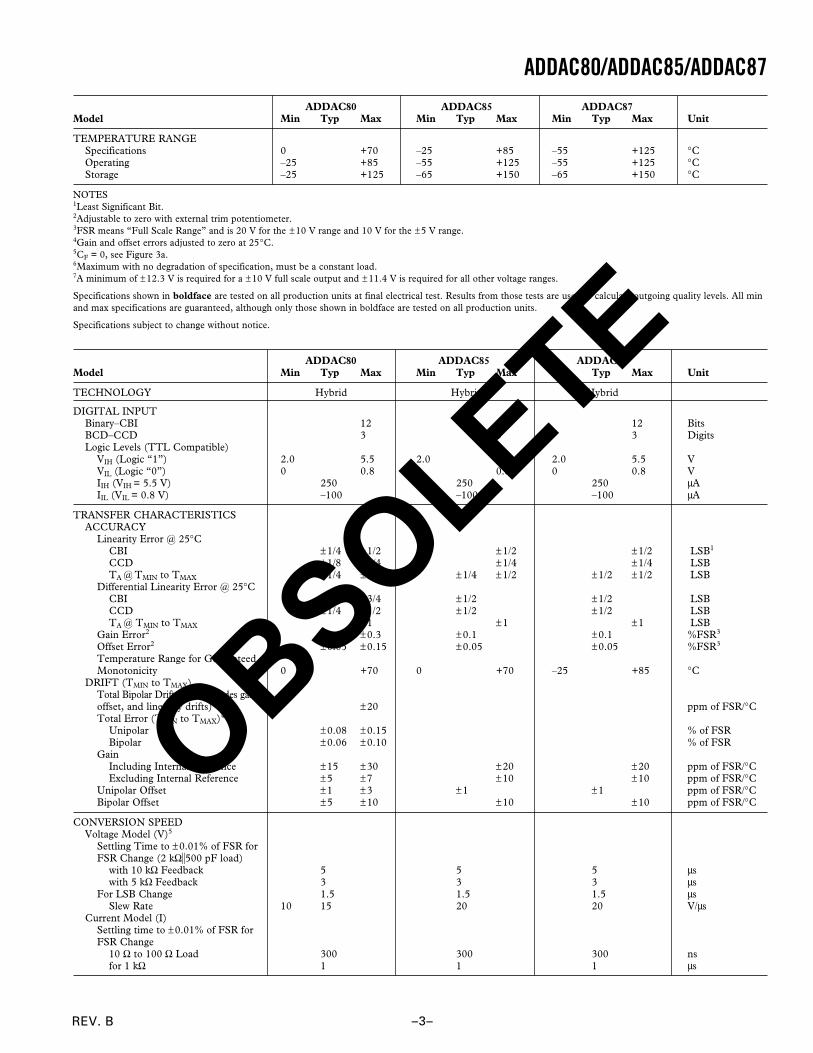
ADDAC80/ADDAC85/ADDAC87–SPECIFICATIONSADDAC80 ADDAC85 ADDAC87
Model Min Typ Max Min Typ Max Min Typ Max Unit
TECHNOLOGY Monolithic Monolithic Monolithic
DIGITAL INPUTBinary–CBI 12 12 12 BitsBCD–CCD DigitsLogic Levels (TTL Compatible)
VIH (Logic “1”) 2.0 5.5 2.0 5.5 2.0 5.5 VVIL (Logic “0”) 0 0.8 0 0.8 0 0.8 VIIH (VIH = 5.5 V) 250 250 250 µAIIL (VIL = 0.8 V) 100 100 100 µA
TRANSFER CHARACTERISTICSACCURACY
Linearity Error @ 25°CCBI ±1/2 ±1/2 ±1/2 LSB1
CCD LSBTA @ TMIN to TMAX ±1/4 ±1/2 ±1/4 ±1/2 ±1/2 ±3/4 LSB
Differential Linearity Error @ 25°CCBI ±3/4 ±3/4 ±3/4 LSBCCD LSBTA @ TMIN to TMAX ±3/4 ±1 ±1 LSB
Gain Error2 ±0.1 ±0.3 ±0.1 ±0.2 ±0.1 ±0.2 %FSR3
Offset Error2 ±0.05 ±0.15 ±0.05 ±0.1 ±0.05 ±0.1 %FSR3
Temperature Range for GuaranteedMonotonicity 0 +70 –25 +85 –55 +125 °C
DRIFT (TMIN to TMAX)Total Bipolar Drift, max (includes gain,offset, and linearity drifts) ±20 ±20 ±30 ppm of FSR/°CTotal Error (TMIN to TMAX)4
Unipolar ±0.08 ±0.15 ±0.12 ±0.2 ±0.18 ±0.3 % of FSRBipolar ±0.06 ±0.10 ±0.08 ±0.12 ±0.14 ±0.24 % of FSR
Gain Including Internal Reference ±15 ±30 ±20 ±20 ppm of FSR/°CGain Excluding Internal Reference ±4 ±7 ±10 ±10 ppm of FSR/°CUnipolar Offset ±1 ±3 ±3 ±3 ppm of FSR/°CBipolar Offset ±5 ±10 ±10 ±10 ppm of FSR/°C
CONVERSION SPEEDVoltage Model (V)5
Settling Time to ±0.01% of FSR forFSR Change (2 kΩ500 pF load)
with 10 kΩ Feedback 3 4 3 4 3 4 µswith 5 kΩ Feedback 2 3 2 3 2 3 µs
For LSB Change 1 1 1 µsSlew Rate 10 10 10 V/µs
ANALOG OUTPUTVoltage Models
Ranges–CBI ±2.5, ±5, ±2.5, ±5, ±2.5, ±5, V±10, +5, ±10, +5, ±10, +5, V10 10 10 V
–CCD VOutput Current ±5 ±5 ±5 mAOutput Impedance (dc) 0.05 0.05 0.05 ΩShort Circuit Current 40 40 40 mA
Internal Reference Voltage (VR) 6.23 6.3 6.37 6.23 6.3 6.37 6.23 6.3 6.37 VOutput Impedance 1.5 1.5 1.5 Ω
Max External Current6 2.5 2.5 2.5 mATempco of Drift ±10 ±20 ±10 ±20 ±10 ppm of VR/°C
POWER SUPPLY SENSITIVITY±15 V ± 10%, 5 V supply when applicable 0.002 0.002 0.002 % of FSR/%VS±12 V ± 5% 0.002 0.002 0.002 % of FSR/%VS
POWER SUPPLY REQUIREMENTSRated Voltages ±15 ±15 ±15 VRange
Analog Supplies ±11.47 ±16.5 ±11.47 ±16.5 ±11.47 ±16.5 VLogic Supplies V
Supply Drain+12 V, +15 V 5 10 5 10 5 10 mA–12 V, –15 V 14 20 14 20 14 20 mA
(TA = 25C, rated power suppliesunless otherwise noted.)
OBSOLETE
REV. B –3–
ADDAC80/ADDAC85/ADDAC87 ADDAC80 ADDAC85 ADDAC87
Model Min Typ Max Min Typ Max Min Typ Max Unit
TEMPERATURE RANGESpecifications 0 +70 –25 +85 –55 +125 °COperating –25 +85 –55 +125 –55 +125 °CStorage –25 +125 –65 +150 –65 +150 °C
NOTES1Least Significant Bit.2Adjustable to zero with external trim potentiometer.3FSR means “Full Scale Range” and is 20 V for the ±10 V range and 10 V for the ±5 V range.4Gain and offset errors adjusted to zero at 25°C.5CF = 0, see Figure 3a.6Maximum with no degradation of specification, must be a constant load.7A minimum of ±12.3 V is required for a ±10 V full scale output and ± 11.4 V is required for all other voltage ranges.
Specifications shown in boldface are tested on all production units at final electrical test. Results from those tests are used to calculate outgoing quality levels. All minand max specifications are guaranteed, although only those shown in boldface are tested on all production units.
Specifications subject to change without notice.
ADDAC80 ADDAC85 ADDAC87Model Min Typ Max Min Typ Max Min Typ Max Unit
TECHNOLOGY Hybrid Hybrid Hybrid
DIGITAL INPUTBinary–CBI 12 12 12 BitsBCD–CCD 3 3 3 DigitsLogic Levels (TTL Compatible)
VIH (Logic “1”) 2.0 5.5 2.0 5.5 2.0 5.5 VVIL (Logic “0”) 0 0.8 0 0.8 0 0.8 VIIH (VIH = 5.5 V) 250 250 250 µAIIL (VIL = 0.8 V) –100 –100 –100 µA
TRANSFER CHARACTERISTICSACCURACY
Linearity Error @ 25°CCBI ±1/4 ±1/2 ±1/2 ±1/2 LSB1
CCD ±1/8 ±1/4 ±1/4 ±1/4 LSBTA @ TMIN to TMAX ±1/4 ±1/2 ±1/4 ±1/2 ±1/2 ±1/2 LSB
Differential Linearity Error @ 25°CCBI ±1/2 ±3/4 ±1/2 ±1/2 LSBCCD ±1/4 ±1/2 ±1/2 ±1/2 LSBTA @ TMIN to TMAX ±1 ±1 ±1 LSB
Gain Error2 ±0.1 ±0.3 ±0.1 ±0.1 %FSR3
Offset Error2 ±0.05 ±0.15 ±0.05 ±0.05 %FSR3
Temperature Range for GuaranteedMonotonicity 0 +70 0 +70 –25 +85 °C
DRIFT (TMIN to TMAX)Total Bipolar Drift, max (includes gain,offset, and linearity drifts) ±20 ppm of FSR/°CTotal Error (TMIN to TMAX)4
Unipolar ±0.08 ±0.15 % of FSRBipolar ±0.06 ±0.10 % of FSR
GainIncluding Internal Reference ±15 ±30 ±20 ±20 ppm of FSR/°CExcluding Internal Reference ±5 ±7 ±10 ±10 ppm of FSR/°C
Unipolar Offset ±1 ±3 ±1 ±1 ppm of FSR/°CBipolar Offset ±5 ±10 ±10 ±10 ppm of FSR/°C
CONVERSION SPEEDVoltage Model (V)5
Settling Time to ±0.01% of FSR forFSR Change (2 kΩ500 pF load)
with 10 kΩ Feedback 5 5 5 µswith 5 kΩ Feedback 3 3 3 µs
For LSB Change 1.5 1.5 1.5 µsSlew Rate 10 15 20 20 V/µs
Current Model (I)Settling time to ±0.01% of FSR forFSR Change
10 Ω to 100 Ω Load 300 300 300 nsfor 1 kΩ 1 1 1 µs
OBSOLETE

REV. B–4–
ADDAC80/ADDAC85/ADDAC87–SPECIFICATIONS ADDAC80 ADDAC85 ADDAC87
Model Min Typ Max Min Typ Max Min Typ Max Unit
ANALOG OUTPUTVoltage Models
Ranges–CBI ±2.5, ±5, ±2.5, ±5, ±2.5, ±5,±10, +5, ±10, +5, ±10, +5,+10 +10 +10 V
Ranges–CCD ±10 +10 +10 VOutput Current ±5 ±5 ±5 mAOutput Impedance (dc) 0.05 0.05 0.05 ΩShort Circuit Duration Indefinite to Common Indefinite to Common Indefinite to Common
Current ModelsRanges–Unipolar –2.0 –2.0 –2.0 mARanges–Bipolar ±1.0 ±1.0 ±1.0 mAOutput Impedance
Bipolar 3.2 3.2 3.2 kΩUnipolar 6.6 6.6 6.6 kΩ
Compliance –1.5, +10 –2.5, +10 –2.5, +10 VInternal Reference Voltage (VR) 6.17 6.3 6.43 6.17 6.3 6.43 6.17 6.3 6.43 V
Output Impedance 1.5 1.5 1.5 ΩMax External Current6 2.5 2.5 2.5 mATempco of Drift ±10 ±20 ±10 ±20 ±10 ±20 ppm of VR/°C
POWER SUPPLY SENSITIVITY±15 V ± 10%, 5 V Supply When Applicable ±0.002 ±0.002 ±0.002 % of FSR/%VS
POWER SUPPLY REQUIREMENTSRated Voltages ±15, +5 ±15, +5 ±15, +5 VRange
Analog Supplies ±14 ±16 ±14.5 ±15.5 ±14.5 ±15.5 VLogic Supplies 4.5 16 4.5 15.5 4.5 15.5 V
Supply Drain7
+15 V 10 20 15 20 15 20 mA–15 V 20 35 25 30 25 30 mA+5 V8 8 20 15 20 15 20 mA
TEMPERATURE RANGESpecifications 0 +70 0 +70 –25 +85 °COperating –25 +85 –25 +85 –55 +125 °CStorage –55 +130 –65 +150 –65 +150 °C
NOTES1Least Significant Bit.2Adjustable to zero with external trim potentiometer.3FSR means “Full Scale Range” and is 20 V for the ± 10 V range and 10 V for the ± 5 V range.4Gain and offset errors adjusted to zero at 25°C.5CF = 0, see Figure 3a.6Maximum with no degradation of specification, must be a constant load.7Including 5 mA load.85 V supply required only for CCD versions.
Specifications subject to change without notice.
(continued)
OBSOLETE
REV. B –5–
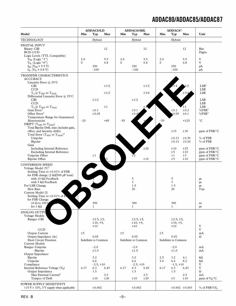
ADDAC80/ADDAC85/ADDAC87ADDAC85LD ADDAC85MIL ADDAC87
Model Min Typ Max Min Typ Max Min Typ Max Unit
TECHNOLOGY Hybrid Hybrid Hybrid
DIGITAL INPUTBinary–CBI 12 12 12 BitsBCD–CCD DigitsLogic Levels (TTL Compatible)
VIH (Logic “1”) 2.0 5.5 2.0 5.5 2.0 5.5 VVIL (Logic “0”) 0 0.8 0 0.8 0 0.8 VIIH (VIH = 5.5 V) 250 250 250 µAIIL (VIL = 0.8 V) –100 –100 –100 µA
TRANSFER CHARACTERISTICSACCURACY
Linearity Error @ 25°CCBI ±1/2 ±1/2 ±1/4 ±1/2 LSB1
CCD LSBTA @ TMIN to TMAX ±1/2 ±3/4 ±3/4 LSB
Differential Linearity Error @ 25°CCBI ±1/2 ±1/2 ±1/2 LSBCCD LSBTA @ TMIN to TMAX ±1 ±1 ±1 LSB
Gain Error2 ±0.1 ±0.1 ±0.1 ±0.2 %FSR3
Offset Error2 ±0.05 ±0.05 ±0.05 ±0.1 %FSR3
Temperature Range for GuaranteedMonotonicity –25 +85 –55 +125 –55 +125 °C
DRIFT (TMIN to TMAX)Total Bipolar Drift, max (includes gain,offset, and linearity drifts) ±15 ±30 ppm of FSR/°CTotal Error (TMIN to TMAX)4
Unipolar ±0.13 ±0.30 % of FSRBipolar ±0.12 ±0.24 % of FSR
GainIncluding Internal Reference ±10 ±20 ±10 ±25 ppm of FSR/°CExcluding Internal Reference ±5 ±10 ppm of FSR/°C
Unipolar Offset ±1 ±2 ±1 ±3 ppm of FSR/°CBipolar Offset ±5 ±10 ±5 ±10 ppm of FSR/°C
CONVERSION SPEEDVoltage Model (V)5
Settling Time to ±0.01% of FSRfor FSR change (2 kΩ500 pF load)
with 10 kΩ Feedback 5 5 5 µswith 5 kΩ Feedback 3 3 3 µs
For LSB Change 1.5 1.5 1.5 µsSlew Rate 20 20 20 V/µs
Current Model (I)Settling Time to ±0.01% of FSRfor FSR Change
10 Ω to 100 Ω Load 300 300 300 nsfor 1 kΩ 1 1 1 µs
ANALOG OUTPUTVoltage Models
Ranges–CBI ±2.5, ±5, ±2.5, ±5, ±2.5, ±5,±10, +5, ±10, +5, ±10, +5,+10 +10 +10 V
Ranges–CCD VOutput Current ±5 ±5 ±5 mAOutput Impedance (dc) 0.05 0.05 0.05 ΩShort Circuit Duration Indefinite to Common Indefinite to Common Indefinite to Common
Current ModelsRanges–Unipolar –2.0 –2.0 –2.0 mARanges–Bipolar ±1.0 ±1.0 ±1.0 mAOutput Impedance
Bipolar 3.2 3.2 2.5 3.2 4.1 kΩUnipolar 6.6 6.6 5.0 6.6 8.2 kΩ
Compliance –2.5, +10 –2.5, +10 –1.5, +10 VInternal Reference Voltage (VR) 6.17 6.3 6.43 6.17 6.3 6.43 6.17 6.3 6.43 V
Output Impedance 1.5 1.5 1.5 ΩMax External Current6 2.5 2.5 2.5 mATempco of Drift ±10 ±20 ±10 ±20 ±5 ±10 ppm of VR/°C
POWER SUPPLY SENSITIVITY±15 V ± 10%, 5 V supply when applicable ±0.002 ±0.002 ±0.002 ±0.003 % of FSR/%VS
OBSOLETE
REV. B–6–
ADDAC80/ADDAC85/ADDAC87–SPECIFICATIONSADDAC85LD ADDAC85MIL ADDAC87
Model Min Typ Max Min Typ Max Min Typ Max Unit
POWER SUPPLY REQUIREMENTSRated Voltages ±15, 5 ±15, 5 ±15, 5 VRange
Analog Supplies ±14.5 ±15.5 ±14.5 ±15.5 ±13.5 ±16.5 VLogic Supplies +4.5 ±15.5 +4.5 +15.5 +4.5 ±16.5 V
Supply Drain7
+15 V 15 20 15 20 10 20 mA–15 V 25 30 25 30 20 35 mA+5 V8 15 20 15 20 10 20 mA
TEMPERATURE RANGESpecification –25 +85 –55 +125 –55 +125 °COperating –55 +125 –55 +125 –55 +125 °CStorage –55 +125 –55 +125 –65 +150 °C
NOTES1Least Significant Bit.2Adjustable to zero with external trim potentiometer.3FSR means “Full-Scale Range” and is 20 V for the ± 10 V range and 10 V for the ± 5 V range.4Gain and offset errors adjusted to zero at 25°C.5CF = 0, see Figure 3a.6Maximum with no degradation of specification, must be a constant load.7Including 5 mA load.85 V supply required only for CCD versions.
Specifications subject to change without notice.
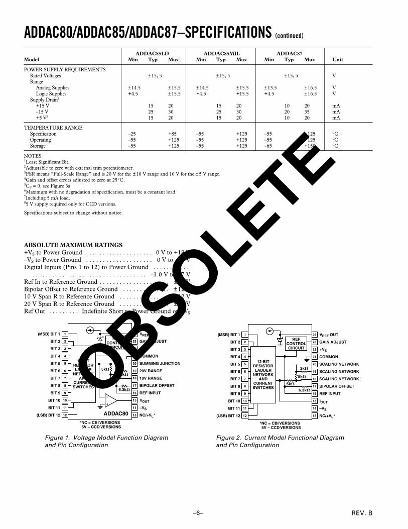
ABSOLUTE MAXIMUM RATINGS+VS to Power Ground . . . . . . . . . . . . . . . . . . . . 0 V to +18 V–VS to Power Ground . . . . . . . . . . . . . . . . . . . . 0 V to –18 VDigital Inputs (Pins 1 to 12) to Power Ground . . . . . . . . . . .
. . . . . . . . . . . . . . . . . . . . . . . . . . . . . . . . . . –1.0 V to +7 VRef In to Reference Ground . . . . . . . . . . . . . . . . . . . . . ±12 VBipolar Offset to Reference Ground . . . . . . . . . . . . . . ±12 V10 V Span R to Reference Ground . . . . . . . . . . . . . . . ±12 V20 V Span R to Reference Ground . . . . . . . . . . . . . . . ±24 VRef Out . . . . . . . . . Indefinite Short to Power Ground or +VS
*NC = CBI VERSIONS 5V – CCD VERSIONS
(MSB) BIT 1
BIT 2
BIT 3
BIT 4
BIT 5
BIT 6
BIT 7
BIT 8
BIT 9
BIT 10
BIT 11
(LSB) BIT 12
VREF OUT
GAIN ADJUST
+VS
COMMON
SUMMING JUNCTION
20V RANGE
10V RANGE
BIPOLAR OFFSET
REF INPUT
VOUT
–VS
NC/+VL*
12-BITRESISTORLADDER
NETWORKAND
CURRENTSWITCHES
REFCONTROLCIRCUIT
1
2
3
4
5
6
7
8
9
10
11
12
24
23
22
21
20
19
18
17
16
15
14
13
6.3k
5k
5k
ADDAC80
+
–
Figure 1. Voltage Model Function Diagramand Pin Configuration
*NC = CBI VERSIONS 5V – CCD VERSIONS
(MSB) BIT 1
BIT 2
BIT 3
BIT 4
BIT 5
BIT 6
BIT 7
BIT 8
BIT 9
BIT 10
BIT 11
(LSB) BIT 12
VREF OUT
GAIN ADJUST
+VS
COMMON
SCALING NETWORK
SCALING NETWORK
SCALING NETWORK
BIPOLAR OFFSET
REF INPUT
IOUT
–VS
NC/+VL*
12-BITRESISTORLADDER
NETWORKAND
CURRENTSWITCHES
REFCONTROLCIRCUIT
1
2
3
4
5
6
7
8
9
10
11
12
24
23
22
21
20
19
18
17
16
15
14
13
6.3k
2k
5k
5k
Figure 2. Current Model Functional Diagramand Pin Configuration
(continued)
OBSOLETE
REV. B
ADDAC80/ADDAC85/ADDAC87
–7–
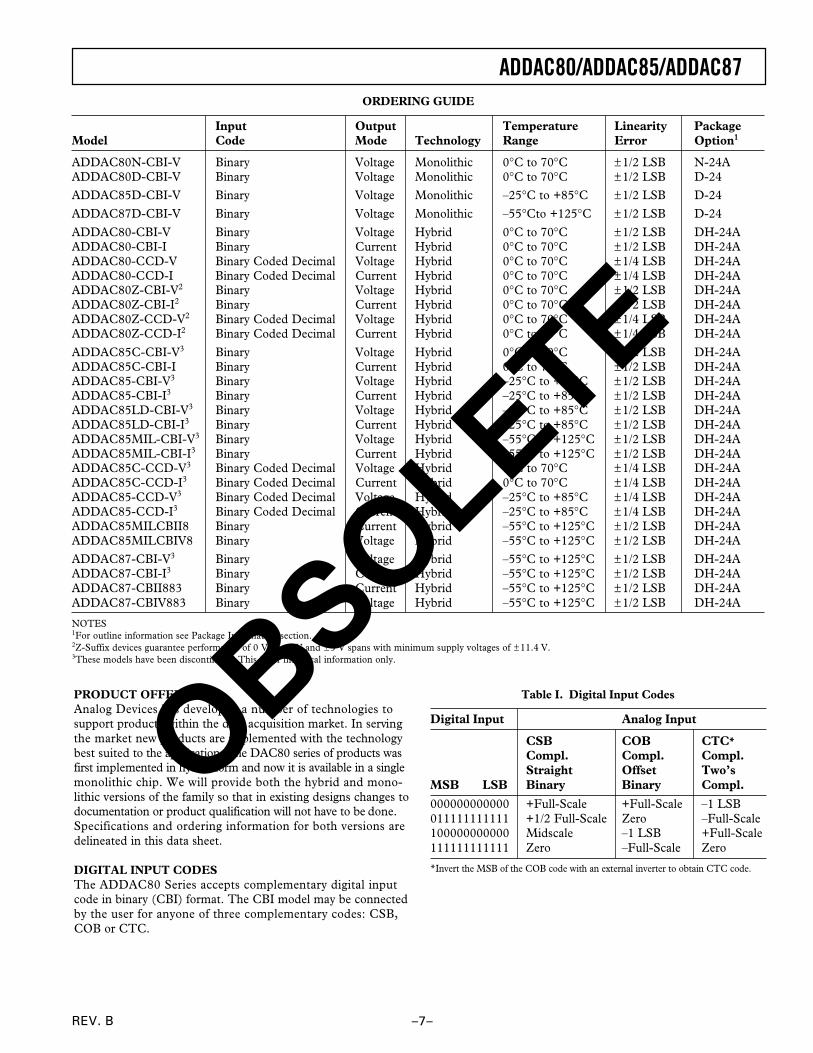
ORDERING GUIDE
Input Output Temperature Linearity PackageModel Code Mode Technology Range Error Option1
ADDAC80N-CBI-V Binary Voltage Monolithic 0°C to 70°C ±1/2 LSB N-24AADDAC80D-CBI-V Binary Voltage Monolithic 0°C to 70°C ±1/2 LSB D-24
ADDAC85D-CBI-V Binary Voltage Monolithic –25°C to +85°C ±1/2 LSB D-24
ADDAC87D-CBI-V Binary Voltage Monolithic –55°Cto +125°C ±1/2 LSB D-24
ADDAC80-CBI-V Binary Voltage Hybrid 0°C to 70°C ±1/2 LSB DH-24AADDAC80-CBI-I Binary Current Hybrid 0°C to 70°C ±1/2 LSB DH-24AADDAC80-CCD-V Binary Coded Decimal Voltage Hybrid 0°C to 70°C ±1/4 LSB DH-24AADDAC80-CCD-I Binary Coded Decimal Current Hybrid 0°C to 70°C ±1/4 LSB DH-24AADDAC80Z-CBI-V2 Binary Voltage Hybrid 0°C to 70°C ±1/2 LSB DH-24AADDAC80Z-CBI-I2 Binary Current Hybrid 0°C to 70°C ±1/2 LSB DH-24AADDAC80Z-CCD-V2 Binary Coded Decimal Voltage Hybrid 0°C to 70°C ±1/4 LSB DH-24AADDAC80Z-CCD-I2 Binary Coded Decimal Current Hybrid 0°C to 70°C ±1/4 LSB DH-24A
ADDAC85C-CBI-V3 Binary Voltage Hybrid 0°C to 70°C ±1/2 LSB DH-24AADDAC85C-CBI-I Binary Current Hybrid 0°C to 70°C ±1/2 LSB DH-24AADDAC85-CBI-V3 Binary Voltage Hybrid –25°C to +85°C ±1/2 LSB DH-24AADDAC85-CBI-I3 Binary Current Hybrid –25°C to +85°C ±1/2 LSB DH-24AADDAC85LD-CBI-V3 Binary Voltage Hybrid –25°C to +85°C ±1/2 LSB DH-24AADDAC85LD-CBI-I3 Binary Current Hybrid –25°C to +85°C ±1/2 LSB DH-24AADDAC85MIL-CBI-V3 Binary Voltage Hybrid –55°C to +125°C ±1/2 LSB DH-24AADDAC85MIL-CBI-I3 Binary Current Hybrid –55°C to +125°C ±1/2 LSB DH-24AADDAC85C-CCD-V3 Binary Coded Decimal Voltage Hybrid 0°C to 70°C ±1/4 LSB DH-24AADDAC85C-CCD-I3 Binary Coded Decimal Current Hybrid 0°C to 70°C ±1/4 LSB DH-24AADDAC85-CCD-V3 Binary Coded Decimal Voltage Hybrid –25°C to +85°C ±1/4 LSB DH-24AADDAC85-CCD-I3 Binary Coded Decimal Current Hybrid –25°C to +85°C ±1/4 LSB DH-24AADDAC85MILCBII8 Binary Current Hybrid –55°C to +125°C ±1/2 LSB DH-24AADDAC85MILCBIV8 Binary Voltage Hybrid –55°C to +125°C ±1/2 LSB DH-24A
ADDAC87-CBI-V3 Binary Voltage Hybrid –55°C to +125°C ±1/2 LSB DH-24AADDAC87-CBI-I3 Binary Current Hybrid –55°C to +125°C ±1/2 LSB DH-24AADDAC87-CBII883 Binary Current Hybrid –55°C to +125°C ±1/2 LSB DH-24AADDAC87-CBIV883 Binary Voltage Hybrid –55°C to +125°C ±1/2 LSB DH-24A
NOTES1For outline information see Package Information section.2Z-Suffix devices guarantee performance of 0 V to +5 V and ±5 V spans with minimum supply voltages of ± 11.4 V.3These models have been discontinued. This is for historical information only.
PRODUCT OFFERINGAnalog Devices has developed a number of technologies tosupport products within the data acquisition market. In servingthe market new products are implemented with the technologybest suited to the application. The DAC80 series of products wasfirst implemented in hybrid form and now it is available in a singlemonolithic chip. We will provide both the hybrid and mono-lithic versions of the family so that in existing designs changes todocumentation or product qualification will not have to be done.Specifications and ordering information for both versions aredelineated in this data sheet.
DIGITAL INPUT CODESThe ADDAC80 Series accepts complementary digital inputcode in binary (CBI) format. The CBI model may be connectedby the user for anyone of three complementary codes: CSB,COB or CTC.
Table I. Digital Input Codes
Digital Input Analog Input
CSB COB CTC*
Compl. Compl. Compl.Straight Offset Two’s
MSB LSB Binary Binary Compl.
000000000000 +Full-Scale +Full-Scale –1 LSB011111111111 +1/2 Full-Scale Zero –Full-Scale100000000000 Midscale –1 LSB +Full-Scale111111111111 Zero –Full-Scale Zero
*Invert the MSB of the COB code with an external inverter to obtain CTC code.
OBSOLETE
REV. B
ADDAC80/ADDAC85/ADDAC87
–8–
ACCURACYAccuracy error of a D/A converter is the difference between theanalog output that is expected when a given digital code isapplied and the output that is actually measured with that codeapplied to the converter. Accuracy error can be caused by gainerror, zero error, linearity error, or any combination of the three.Of these three specifications, the linearity error specification isthe most important since it cannot be corrected. Linearity erroris specified over its entire temperature range. This means thatthe analog output will not vary by more than its maximumspecification, from an ideal straight line drawn between theend points (inputs all “1”s and all “0”s) over the specifiedtemperature range.
Differential linearity error of a D/A converter is the deviationfrom an ideal 1 LSB voltage change from one adjacent outputstate to the next. A differential linearity error specification of±1/2 LSB means that the output voltage step sizes can rangefrom 1/2 LSB to 1 1/2 LSB when the input changes from oneadjacent input state to the next.
DRIFTGain DriftA measure of the change in the full scale range output overtemperature expressed in parts per million of full scale rangeper °C (ppm of FSR/°C). Gain drift is established by: 1) testingthe end point differences for each ADDAC80 model at thelowest operating temperature, 25°C and the highest operatingtemperature; 2) calculating the gain error with respect to the25°C value and; 3) dividing by the temperature change.
Offset DriftA measure of the actual change in output with all “1”s on theinput over the specified temperature range. The maximumchange in offset is referenced to the offset at 25°C and isdivided by the temperature range. This drift is expressed inparts per million of full scale range per °C (ppm of FSR/°C).
SETTLING TIMESettling time for each model is the total time (including slewtime) required for the output to settle within an error bandaround its final value after a change in input.
Voltage Output ModelsThree settling times are specified to 0.01% of full scale range(FSR); two for maximum full scale range changes of 20 V, 10 Vand one for a 1 LSB change. The 1 LSB change is measured atthe major carry (0 1 1 1 . . . 1 1 to 1 0 0 0 . . . 0 0), the point atwhich the worst case settling time occurs. The settling timecharacteristic depends on the compensation capacitor selected,the optimum value is 25 pF as shown in Figure 3a.
Current Output ModelsTwo settling times are specified to ±0.01% of FSR. Each is givenfor current models connected with two different resistive loads:10 Ω to 100 Ω and 1000 Ω to 1875 Ω. Internal resistors are providedfor connecting nominal load resistances of approximately 1000 Ωto 1800 Ω for output voltage ranges of ±1 V and 0 V to –2 V.
10V
VOUTDATAIN
SUMMINGJUNCTION
1–12
18
20
100pF
2k
10V
HP6216A
TEKTRONIX7A1315
CF25pF
Figure 3a. Voltage Model Settling Time Circuit
10
0%
100
90
5V>1mV
500ns5V
Figure 3b. Voltage Model Settling Time CF = 25 pF
POWER SUPPLY SENSITIVITYPower supply sensitivity is a measure of the effect of a powersupply change on the D/A converter output. It is defined as apercent of FSR per percent of change in either the positive ornegative supplies about the nominal power supply voltages.
REFERENCE SUPPLYAll models are supplied with an internal 6.3 V reference voltagesupply. This voltage (Pin 24) is accurate to ±1% and must beconnected to the Reference Input (Pin 16) for specified opera-tion. This reference may also be used externally with externalcurrent drain limited to 2.5 mA. An external buffer amplifier isrecommended if this reference is to be used to drive other sys-tem components. Otherwise, variations in the load driven by thereference will result in gain variations. All gain adjustmentsshould be made under constant load conditions.
ANALYZING DEVICE ACCURACY OVER THETEMPERATURE RANGEFor the purposes of temperature drift analysis, the major devicecomponents are shown in Figure 4. The reference element andbuffer amplifier drifts are combined to give the total referencetemperature coefficient. The input reference current to theDAC, IREF, is developed from the internal reference and willshow the same drift rate as the reference voltage. The DACoutput current, IDAC, which is a function of the digital inputcodes, is designed to track IREF; if there is a slight mismatch inthese currents over temperature, it will contribute to the gainT.C. The bipolar offset resistor, RBP, and gain setting resistor,RGAIN, also have temperature coefficients that contribute tosystem drift errors. The input offset voltage drift of the outputamplifier, OA, also contributes a small error.
OBSOLETE

REV. B
ADDAC80/ADDAC85/ADDAC87
–9–
15V
+
–
IREFDAC
IDAC
V–
+
–OA
RGAINRBP
6.3k6.3V
Figure 4. Bipolar Configuration
There are three types of drift errors over temperature: offset,gain, and linearity. Offset drift causes a vertical translation ofthe entire transfer curve; gain drift is a change in the slope of thecurve; and linearity drift represents a change in the shape of thecurve. The combination of these three drifts results in the com-plete specification for total error over temperature.
Total error is defined as the deviation from a true straight linetransfer characteristic from exactly zero at a digital input thatcalls for zero output to a point that is defined as full-scale. Aspecification for total error over temperature assumes that boththe zero and full-scale points have been trimmed for zero errorat 25°C. Total error is normally expressed as a percentage of thefull-scale range. In the bipolar situation, this means the totalrange from –VFS to +VFS.
Several new design concepts not previously used in DAC80-typedevices contribute to a reduction in all the error factors overtemperature. The incorporation of low temperature coefficientsilicon-chromium thin-film resistors deposited on a single chip,a patented, fully differential, emitter weighted, precision currentsteering cell structure, and a T.C. trimmed buried Zener diodereference element results in superior wide temperature rangeperformance. The gain setting resistors and bipolar offset resis-tor are also fabricated on the chip with the same SiCr materialas the ladder network, resulting in low gain and offset drift.
MONOTONICITY AND LINEARITYThe initial linearity error of ±1/2 LSB max and the differentiallinearity error of ±3/4 LSB max guarantee monotonic performanceover the specified range. It can therefore be assumed that linearityerrors are insignificant in computation of total temperature errors.
UNIPOLAR ERRORSTemperature error analysis in the unipolar mode is straightforward:there is an offset drift and a gain drift. The offset drift (whichcomes from leakage currents and drift in the output amplifier(OA)) causes a linear shift in the transfer curve as shown inFigure 5. The gain drift causes a change in the slope of thecurve and results from reference drift, DAC drift, and drift inRGAIN relative to the DAC resistors.
BIPOLAR RANGE ERRORSThe analysis is slightly more complex in the bipolar mode. Inthis mode RBP is connected to the summing node of the outputamplifier (see Figure 4) to generate a current that exactly balancesthe current of the MSB so that the output voltage is zero withonly the MSB on.
Note that if the DAC and application resistors track perfectly,the bipolar offset drift will be zero even if the reference drifts. Achange in the reference voltage, which causes a shift in the bipolaroffset, will also cause an equivalent change in IREF and thus IDAC,so that IDAC will always be exactly balanced by IBP with the MSBturned on. This effect is shown in Figure 5. The net effect of thereference drift then is simply to cause a rotation in the transferaround bipolar zero. However, consideration of second ordereffects (which are often overlooked) reveals the errors in thebipolar mode. The unipolar offset drifts previously discussedwill have the same effect on the bipolar offset. A mismatch of RBP
to the DAC resistors is usually the largest component of bipolardrift, but in the ADDAC80 this error is held to 10 ppm/°C max.Gain drift in the DAC also contributes to bipolar offset drift,as well as full-scale drift, but again is held to 10 ppm/°C max.
ACTUAL GAIN SHIFT
IDEAL
OFFSET (ZERO) SHIFT
OU
TP
UT
UNIPOLARINPUT
OU
TP
UT
OFFSET SHIFT
BIPOLAR (IDEAL CASE)
GAIN SHIFT
INPUT
Figure 5. Unipolar and Bipolar Drifts
USING THE ADDAC80 SERIESPOWER SUPPLY CONNECTIONSFor optimum performance power supply decoupling capacitorsshould be added as shown in the connection diagrams. Thesecapacitors (1 µF electrolytic recommended) should be locatedclose to the ADDAC80. Electrolytic capacitors, if used, shouldbe paralleled with 0.01 µF ceramic capacitors for optimum highfrequency performance.
EXTERNAL OFFSET AND GAIN ADJUSTMENTOffset and gain may be trimmed by installing external OFFSETand GAIN potentiometers. These potentiometers should beconnected as shown in the block diagrams and adjusted asdescribed below. TCR of the potentiometers should be 100 ppm/°Cor less. The 3.9 MΩ and 10 MΩ resistors (20% carbon or better)should be located close to the ADDAC80 to prevent noise pickup.If it is not convenient to use these high-value resistors, a function-ally equivalent “T” network, as shown in Figure 8 may besubstituted in each case. The gain adjust (Pin 23) is a highimpedance point and a 0.01 µF ceramic capacitor should beconnected from this pin to common to prevent noise pickup.
OBSOLETE

REV. B
ADDAC80/ADDAC85/ADDAC87
–10–
1F
3.9M
1F
0.01F
10M
+VS
10kTO
100k
+VS
–VS
10kTO
100k
–VS
1
2
3
4
5
6
7
8
9
10
11
12
12-BITRESISTORLADDER
NETWORKAND
CURRENTSWITCHES
REFCONTROLCIRCUIT
6.3k
2k
3k
5k
24
23
22
21
20
19
18
17
16
15
14
13
Figure 6. External Adjustment and Voltage SupplyConnection Diagram, Current Model
Offset AdjustmentFor unipolar (CSB) configurations, apply the digital input codethat should produce zero potential output and adjust theOFFSET potentiometer for zero output. For bipolar (COB, CTC)configurations, apply the digital input code that should producethe maximum negative output voltage. Example: If the FULLSCALE RANGE is connected for 20 V, the maximum negativeoutput voltage is –10 V. See Table II for corresponding codes.
Gain AdjustmentFor either unipolar or bipolar configurations, apply the digitalinput that should give the maximum positive voltage output.Adjust the GAIN potentiometer for this positive full-scale voltage.See Table II for positive full-scale voltages.
12-BITRESISTORLADDER
NETWORKAND
CURRENTSWITCHES
REFCONTROLCIRCUIT
1
2
3
4
5
6
7
8
9
10
11
12
24
23
22
21
20
19
18
17
16
15
14
13
6.3k
5k
5k
+
–
1F
1F
0.01F
10M
+VS
10kTO
100k
+VS
–VS10k
TO100k
–VS
3.9M
Figure 7. External Adjustment and Voltage SupplyConnection Diagram, Voltage Model
10M 270k 270k
7.8k
3.9M 180k 180k
10k
Figure 8. Equivalent Resistances
Table II. Digital Input Analog Output
Digital Input Analog Output
12-Bit Resolution Voltage* Current
MSB LSB 0 to +10 V 10 V 0 to –2 mA 1 mA0 0 0 0 0 0 0 0 0 0 0 0 +9.9976 V +9.9951 V –1.9995 mA –0.9995 mA0 1 1 1 1 1 1 1 1 1 1 1 +5.0000 V 0.0000 V –1.0000 mA 0.0000 mA1 0 0 0 0 0 0 0 0 0 0 0 +4.9976 V 4.88 mV –0.9995 mA +0.0005 mA1 1 1 1 1 1 1 1 1 1 1 1 0.0000 V –10.0000 V 0.0000 mA –1.00 mAl LSB 2.44 mV –0.0049 V 0.488 µA 0.488 µA
*To obtain values for other binary ranges 0 to 5 V range: divide 0 to 10 values by 2; ± 5 V range: divide± 10 V range values by 2; ±2.5 V range: divide ±10 V range values by 4.OBSOLETE

REV. B
ADDAC80/ADDAC85/ADDAC87
–11–
VOLTAGE OUTPUT MODELSInternal scaling resistors provided in the ADDAC80 may beconnected to produce bipolar output voltage ranges of ±10 V,±5 V or ±2.5 V or unipolar output voltage ranges of 0 V to +5 Vor 0 V to +10 V (see Figure 9).
REFINPUT
TO REFCONTROL
CIRCUIT
FROMWEIGHTEDRESISTORNETWORK
SUMMINGJUNCTION
6.3k
5k5k
1820
16
+
– OUTPUT
COM
BIPOLAROFFSET
21
15
19
17
Figure 9. Output Amplifier Voltage Range Scaling Circuit
Gain and offset drift are minimized in the ADDAC80 becauseof the thermal tracking of the scaling resistors with other devicecomponents. Connections for various output voltage ranges areshown in Table III. Settling time is specified for a full-scalerange change: 4 s for a 10 kΩ feedback resistor; 3 s for a 5 kΩfeedback resistor when using the compensation capacitor shownin Figure 3a.
The equivalent resistive scaling network and output circuit ofthe current model are shown in Figures 10 and 11. External RLS
resistors are required to produce exactly 0 V to –2 V or ± 1 Voutput. TCR of these resistors should be ±100 ppm/°C or lessto maintain the ADDAC80 output specifications. If exact outputranges are not required, the external resistors are not needed.
17
TO REF CONTROL CIRCUIT
6.3k
3k 2k19
20
16
18
REF IN
5k
15
Figure 10. Internal Scaling Resistors
6.3kBIPOLAR OFFSET
REFERENCEINPUT
IOUT
COMMON
REFERENCE OUT
6.6k
V
TO REFCONTROLCIRCUIT
17
16
I0 TO 2mA
6.3V
24
21
15
+
–
Figure 11. ADDAC80 Current Model Equivalent Output Circuit
Internal resistors are provided to scale an external op amp or toconfigure a resistive load to offer two output voltage ranges of ±1 Vor 0 V to –2 V. These resistors (RLI TCR = 20 ppm/°C) are anintegral part of the ADDAC80 and maintain gain and bipolaroffset drift specifications. If the internal resistors are not used, exter-nal RL (or RF) resistors should have a TCR of ±25 ppm/°C orless to minimize drift. This will typically add ±50 ppm/°C + theTCR of RL (or RF) to the total drift.
Table III. Output Voltage Range Connections, Voltage Model ADDAC80
Output Digital Connect Connect Connect ConnectRange Input Codes Pin 15 to Pin 17 to Pin 19 to Pin 16 to
±10 V COB or CTC 19 20 15 24±5 V COB or CTC 18 20 NC 24±2.5 V COB or CTC 18 20 20 240 V to 10 V CSB 18 21 NC 240 V to 5 V CSB 18 21 20 240 V to 10 V CCD 19 NC 15 24
NC = No Connect
DRIVING A RESISTIVE LOAD UNIPOLARA load resistance, RL = RLI, + RLS, connected as shown inFigure 12 will generate a voltage range, VOUT, determined by:
V mA
k Rk ROUT
L
L=
×+
–..
26 66 6
ΩΩ
(1)
where RL max = 1.54 kΩ and VOUT max = –2.5 V
To achieve specified drift, connect the internal scaling resistor(RLI) as shown in Table IV to an external metal film trim resistor(RLS) to provide full scale output voltage range of 0 V to –2 V.With RLS = 0 V, VOUT = –1.69 V.
0 TO2mA
CURRENT CONTROLLEDBY DIGITAL INPUT
6.6k
RLI968
COMMON
VOUTRLS
+
–
15
18
21
Figure 12. Equivalent Circuit ADDAC80-CBI-I Connectedfor Unipolar Voltage Output with Resistive Load
OBSOLETE
REV. B
ADDAC80/ADDAC85/ADDAC87
–12–
DRIVING A RESISTOR LOAD BIPOLARThe equivalent output circuit for a bipolar output voltage rangeis shown in Figure 13, RL = RLI + RLS. VOUT is determined by:
V mA
R kR kOUT
L
L
= ± ×+
13 223 22..
ΩΩ (2)
where RL max = 11.18 kΩ and VOUT max = ±2.5 V
To achieve specified drift, connect the internal scaling resistors(RLI) as shown in Table IV for the COB or CTC codes and addan external metal film resistor (RLS) in series to obtain a full scaleoutput range of ±1 V. In this configuration, with RLS equal tozero, the full scale range will be ±0.874 V.
1mA
CURRENT CONTROLLEDBY DIGITAL INPUT
3.22k
RLI1.2k
COMMON
VOUTRLS
+
–
15
20
21
Figure 13. ADDAC80-CBI-I Connected for BipolarOutput Voltage with Resistive Load
DRIVING AN EXTERNAL OP AMPThe current model ADDAC80 will drive the summing junctionof an op amp used as a current to voltage converter to producean output voltage. As seen in Figure 14,
V I ROUT OUT F= × (3)
where IOUT is the ADDAC80 output current and RF is the feed-back resistor. Using the internal feedback resistors of the currentmodel ADDAC80 provides output voltage ranges the same asthe voltage model ADDAC80. To obtain the desired outputvoltage range when connecting an external op amp, refer toTable V and Figure 14.
20V RANGE
5k
I0 TO 2mA
6.6k
5k CBI
10V RANGE
AD509KH* VOUT
*FOR FAST SETTLING TIME
19
18
15
21
A
Figure 14. External Op Amp Using InternalFeedback Resistors
OUTPUT LARGER THAN 20 V RANGEFor output voltage ranges larger than ±10 V, a high voltage opamp may be employed with an external feedback resistor. UseIOUT values of ± l mA for bipolar voltage ranges and –2 mA forunipolar voltage ranges (see Figure 15). Use protection diodeswhen a high voltage op amp is used.
The feedback resistor, RF, should have a temperature coefficientas low as possible. Using an external feedback resistor, overalldrift of the circuit increases due to the lack of temperature track-ing between RF and the internal scaling resistor network. This willtypically add 50 ppm/°C + RF drift to total drift.
17
16
15
24
21
V
+
–
I0 TO 2mA
VREF6.3V
6.6k
6.3k
*FOR OUTPUT VOLTAGE SWINGS UP TO 140V p-p
VOUT
RF
171K*
Figure 15. External Op Amp Using ExternalFeedback Resistors
Table IV. Current Model/Resistive Load Connections
1%Metal Film RLI Connections Reference Bipolar Offset
Internal ExternalDigital Output Resistance Resistance Connect Connect Connect Connect ConnectInput Codes Range RLI (k) RLS Pin 15 to Pin 18 to Pin 20 to Pin 16 to Pin 17 to RLS
CSB 0 to –2 V 0.968 210 Ω 20 19 and RLS 15 24 Com (21) BetweenPin 18 andCom (21)
COB or CTC ±1 V 1.2 249 Ω 18 19 RLS 24 15 BetweenPin 20 andCom (21)
CCD 0 to ±2 V 3 N/A NC 21 NC 24 NC N/A
OBSOLETE

REV. B
ADDAC80/ADDAC85/ADDAC87
–13–
OUTLINE DIMENSIONSDimensions shown in inches and (mm).
24-Lead Plastic DIP (N-24A)
24
1 12
13
PIN 1
0.580 (14.73)0.485 (12.32)
1.290 (32.70)1.150 (29.30)
0.195 (4.95)0.125 (3.18)
0.015 (0.381)0.008 (0.204)
0.625 (15.87)0.600 (15.24)
SEATINGPLANE
0.060 (1.52)0.015 (0.38)
0.250(6.35)MAX
0.022 (0.558)0.014 (0.356)
0.200 (5.05)0.125 (3.18)
0.150(3.81)MIN
0.100(2.54)BSC
0.070 (1.77)0.030 (0.77)
CONTROLLING DIMENSIONS ARE IN MILLIMETERS: INCH DIMENSIONSARE ROUNDED-OFF MILLIMETER EQUIVALENTS FOR REFERENCEONLY AND ARE NOT APPROPRIATE FOR USE IN DESIGN
24-Lead Ceramic DIP (D-24)
SEATINGPLANE
0.023 (0.58)0.014 (0.36)
0.075 (1.91)0.015 (0.38)0.225 (5.72)
MAX
0.200 (5.08)0.120 (3.05)
0.070 (1.78)0.030 (0.76)
0.150(3.81)MIN
1.290 (32.77) MAX
24
1 12
13
0.610 (15.49)0.500 (12.70)
PIN 1
0.098 (2.49) MAX0.005 (0.13) MIN
0.620 (15.75)0.590 (14.99)
0.015 (0.38)0.008 (0.20)
NOTES1. INDEX AREA; A NOTCH OR A LEAD ONE IDENTIFICATION MARK IS LOCATED ADJACENT TO LEAD ONE.2. THE MINIMUM LIMIT FOR DIMENSION MAY BE 0.023" (0.58 mm) FOR ALL FOUR CORNER LEADS ONLY.3. DIMENSION SHALL BE MEASURED FROM THE SEATING PLANE TO THE BASE PLANE.4. THIS DIMENSION ALLOWS FOR OFF-CENTER LID, MENISCUS AND GLASS OVERRUN.5. APPLIES TO ALL FOUR CORNERS.6. ALL LEADS — INCREASE MAXIMUM LIMIT BY 0.003" (0.08 mm) MEASURED AT THE CENTER OF THE FLAT, WHEN HOT SOLDER DIP LEAD FINISH IS APPLIED.7. TWENTY TWO SPACES.8. CONTROLLING DIMENSIONS ARE IN MILLIMETERS. INCH DIMENSIONS ARE ROUNDED-OFF MILLIMETER EQUIVALENTS FOR REFERENCE ONLY AND ARE NOT APPROPRIATE FOR USE IN DESIGN
SEE NOTE 5
SEE NOTE 1
SEE NOTE 7
SEE NOTE 3
SEE NOTE 2, 6
SEE NOTE 4
0.110 (2.79)0.090 (2.29)
SEE NOTE 4
SEE NOTE 6
Table V. External Op Amp Voltage Mode Connections
Output Digital Connect Connect Connect ConnectRange Input Codes A to Pin 17 to Pin 19 to Pin 16 to
±10 V COB or CTC 19 15 A 24±5 V COB or CTC 18 15 NC 24±2.5 V COB or CTC 18 15 15 240 V to 10 V CSB 18 21 NC 240 V to 5 V CSB 18 21 15 24
OBSOLETE

REV. B
ADDAC80/ADDAC85/ADDAC87
–14–
OUTLINE DIMENSIONSDimensions shown in inches and (mm).
24-Lead Side Brazed Ceramic DIP for Hybrid (DH-24A)
SEATINGPLANE
0.023 (0.58)0.014 (0.36)
0.075 (1.91)0.015 (0.38)
0.225 (5.72)MAX
0.200 (5.08)0.120 (3.05)
0.070 (1.78)0.030 (0.76)
0.180(4.57)MIN
1.212 (29.69) MAX
0.100 (2.54)BSC
0.098 (2.49) MAX0.005 (0.13) MIN
0.620 (15.75)0.590 (14.99)
0.015 (0.38)0.008 (0.20)
24
12
13
1PIN 1
NOTES1. INDEX AREA; A NOTCH OR A LEAD ONE IDENTIFICATION MARK IS LOCATED ADJACENT TO LEAD ONE.2. THE MINIMUM LIMIT FOR DIMENSION MAY BE 0.023" (0.58 mm) FOR ALL FOUR CORNER LEADS ONLY.3. DIMENSION SHALL BE MEASURED FROM THE SEATING PLANE TO THE BASE PLANE.4. THE BASIC PIN SPACING IS 0.100" (2.54 mm) BETWEEN CENTERLINES.5. APPLIES TO ALL FOUR CORNERS.6. SHALL BE MEASURED AT THE CENTERLINE OF THE LEADS.7. TWENTY TWO SPACES.8. CONTROLLING DIMENSIONS ARE IN MILLIMETERS: INCH DIMENSIONS ARE ROUNDED-OFF MILLIMETER EQUIVALENTS FOR REFERENCE ONLY AND ARE NOT APPROPRIATE FOR USE IN DESIGN.
SEE NOTE 5
SEE NOTE 1
SEE NOTE 2SEE NOTE 6
SEE NOTE 3
SEE NOTE 4, 7
0.600 (14.70)0.580 (14.21)
OBSOLETE

REV. B
ADDAC80/ADDAC85/ADDAC87
–15–
Revision HistoryLocation Page
Data Sheet changed from REV. A to REV. B.
Update OUTLINE DIMENSION drawings . . . . . . . . . . . . . . . . . . . . . . . . . . . . . . . . . . . . . . . . . . . . . . . . . . . . . . . . . . . . . . . . . . . 1
OBSOLETE

–16–
C00
381–
0–1/
02(B
)P
RIN
TE
D IN
U.S
.A.OBSOLETE