A 10-BIT 50 MEGA-SAMPLES-PER-SECOND PIPELINED...
30
A 10-BIT 50 MEGA-SAMPLES-PER-SECOND PIPELINED ANALOG-TO-DIGITAL CONVERTER YUZMAN BIN YUSOFF UNIVERSITI TEKNOLOGI MALAYSIA
Transcript of A 10-BIT 50 MEGA-SAMPLES-PER-SECOND PIPELINED...

A 10-BIT 50 MEGA-SAMPLES-PER-SECOND PIPELINED
ANALOG-TO-DIGITAL CONVERTER
YUZMAN BIN YUSOFF
UNIVERSITI TEKNOLOGI MALAYSIA

A 10-BIT 50 MEGA-SAMPLES-PER-SECOND PIPELINED ANALOG-TO-
DIGITAL CONVERTER
YUZMAN BIN YUSOFF
A thesis submitted in fulfilment of the
requirements for the awards of the degree of
Master of Engineering (Electrical)
Faculty of Electrical Engineering
Universiti Teknologi Malaysia
OCTOBER 2010

iii
ACKNOWLEDGMENTS
First, I would like to express my deep appreciation to my supervisor and co-
supervisor, Dr. Muhammad Nadzir Marsono and Mr. Mohd Shahiman Sulaiman, for
their invaluable guidance, their kindness, and support throughout my long journey as a
graduate student. Without their encouragement and patient support, this work would not
have been possible.
Thanks to Mr. Reza Lotfi from Mars Semiconductor Technology for his helps
on MATLAB programming.
I would like to thank my fellow colleague, Mr Wee Leong Son and friends from
Microelectronics department in MIMOS Berhad for their helps, suggestions and
inspirations toward the success of this project.
My warmest appreciation also goes to my family who has given their unfailing
support and patience; especially to my beloved wife.
Finally, I want to acknowledge the financial support from MIMOS Berhad
throughout my studies.

iv
ABSTRACT
Most of modern communication devices are implemented on portable systems
powered by a battery with limited energy. Due to their dependence on batteries, some
efforts have to be made to minimize the power consumption of these devices. One of
the approaches is to use low power analog-to-digital converter (ADC). This thesis
focuses on the design implementation of low power pipelined ADC for wireless
communication system. The pipelined ADC was realized using 1.5-bit per-stage
structures with digital error correction. For power reduction, dedicated front-end
sample-and-hold circuit used in conventional pipelined ADC architecture is removed.
Furthermore, power analysis has been performed using MATLAB® to assist in
determining the best stage resolution in pipelined stages. A dynamic comparator is
employed to optimize further the power consumption in pipelined stages. This low
power pipelined ADC is implemented using Siltera’s 0.18µm, 1.8-3.3V complementary
metal oxide semiconductor process, with double layer poly-silicon and five metal
layers. The designed pipelined ADC exhibits a 10-bit resolution at 50 Mega-Sample
per-second and 50.82dB signal to noise and distortion ratio with an effective number of
bits of 8.15-bit. The differential non-linearity (DNL) and the integral non-linearity
(INL) are ±1 least-significant of bits (LSB). The power consumption is 97mW from a
3V supply and the entire area of the pipelined ADC including input and output pads is
2.4mm2.

v
ABSTRAK
Hampir keseluruhan alat komunikasi moden diimplementasi pada sistem mudah alih
yang dikuasai oleh tenaga bateri yang terbatas. Disebabkan oleh kebergantungan alat-alat
kominukasi ini kepada bateri, sesuatu usaha perlu dilakukan untuk mengurangkan
penggunaan kuasa mereka. Salah satu pendekatan ialah dengan menggunakan penukar
analog kepada digital (analog-digital) yang berkuasa rendah. Tesis ini memberi tumpuan
pada pelaksanaan rekabentuk penukar analog kepada digital jenis talian paip kuasa rendah
untuk digunakan di dalam sistem komunikasi tanpa wayar. Penukar analog-digital talian
paip ini dihasilkan dengan menggunakan struktur 1.5-bit disetiap peringkat bersama dengan
litar pembetulan ralat. Untuk mengurangkan penggunaan kuasa, litar khusus untuk sampel
dan pegang yang lazimnya digunakan di bahagian hadapan kebanyakan senibina penukar
analog-digital talian paip telah disingkirkan. Tambahan lagi, analisis mengenai penggunaan
kuasa di dalam beberapa struktur rekabentuk telah dilakukan dengan bantuan perisian
MATLAB® bagi menentukan senibina terbaik untuk resolusi di dalam setiap peringkat
talian-talian paip ini. Pembanding dinamik juga turut digunakan untuk mengurangkan lagi
penggunaan kuasa di dalam semua peringkat talian-talian paip ini. Penukar analog-digital
yang berkuasa rendah ini telah dihasilkan dengan menggunakan teknologi 0.18µm
pelengkap logam oksida semiconduktor daripada Siltera dengan dua lapisan polisilikon dan
lima lapisan logam. Penukar analog-digital yang telah direkabentuk ini berjaya mencapai
resolusi 10-bit pada kelajuan 50 Mega sampel per satu saat dan nisbah isyarat kepada
hingar dan herotan adalah 50.82dB. Disamping itu, nombor bit berkesan ialah 8.15-bit.
Nilai ketaklurusan kebezaan dan ketaklurusan kamiran masing-masing ialah ±1 bit bererti
terkecil. Penggunaan kuasa oleh penukar analog-digital yang direkabentuk ini ialah
sebanyak 97mW pada voltan bekalan 3V dan seluruh keluasan bentangan termasuk pad
masukan dan keluaran ialah 2.4mm2.
vi
TABLE OF CONTENTS
CHAPTER TITLE PAGE
DECLARATION ii
ACKNOWLEDGEMENTS iii
ABSTRACT iv
ABSTRAK v
TABLE OF CONTENTS vi
LIST OF TABLES x
LIST OF FIGURES xi
LIST OF ABBREVIATIONS xv
LIST OF APPENDICES xvii
LIST OF PUBLICATIONS xviii
1 INTRODUCTION 1
1.1 Motivation 2
1.2 Problem Statement 4
1.3 Research Contribution 5
1.4 Thesis Organization 6
2 LITERATURE REVIEWS 7
2.1 Performance parameters 7
2.1.1 Differential and Integral Non-Linearity 8
2.1.2 Signal-to-Noise Ratio 9

vii
2.1.3 Total Harmonic Distortion 10
2.1.4 Signal-to-Noise Distortion Ratio 10
2.1.5 Spurious Free Dynamic Range 10
2.1.6 Effective Number of Bits 11
2.1.7 Latency 11
2.2 Overview of Analog-to-Digital Converter Architecture (ADC) 12
2.2.1 Flash ADC 12
2.2.2 Successive Approximation ADC 13
2.2.3 Pipelined ADC 14
2.2.4 Over-Sampled ADC 15
2.2.5 Summary of ADC Architectures 15
2.3 Basic Building of Pipelined ADC 17
2.3.1 Multiplying Digital-to-Analog Converter (DAC) 17
2.3.2 Sub-ADC 21
2.3.3 Operational Amplifiers 22
2.3.4 Comparator 31
2.3.5 Digital Error Correction 33
2.4 Chapter Summary 34
3 SYSTEM DESIGN ARCHITECTURE 35
3.1 ADC Specifications 35
3.2 Power Optimization 36
3.2.1 Bit Per Stage Architecture 36
3.2.2 Sample and Hold Removal 40
3.2.3 Stage and Capacitor Scaling 41
3.3 System Level Simulation 42
3.4 Chapter Summary 44

viii
4 DESIGN IMPLEMENTATIONS 45
4.1 1.5-bit Multiplying DAC 45
4.1.1 Operational Amplifier 46
4.1.2 Common Mode Feedback 50
4.1.3 Bias Circuit 51
4.1.4 Sub-DAC 51
4.1.5 Switches 54
4.1.5.1 Transmission gate 54
4.1.5.2 Bootstrap Switch 55
4.1.6 Non Overlapping Clock Generator 56
4.1.7 MDAC Characterizations 57
4.2 Sub-ADC 59
4.3 Digital Error Correction Circuit 62
4.4 Fully Integrated 10-bit 50MS/s Pipelined ADC 64
4.5 Chapter Summary 66
5 ADC CHARACTERIZATION 67
5.1 Functionality 67
5.2 Static Linearity 70
5.3 Dynamic Linearity 71
5.4 Chapter Summary 74
6 CONCLUSION 76
6.1 Thesis Contributions 76
6.2 Future Work 77

ix
REFERENCES 79
Appendices A-E 85 - 95

x
LIST OF TABLES
TABLE NO. TITLE PAGE
1.1 ADC applications and their design constraints 2
3.1 Design specifications for pipelined ADC for wireless
communication system application. 36
3.2 Different configurations for different pipelined architecture 39
3.3 Pipelined ADC preliminary result using MATLAB 44
3.4 Design requirements for MDAC design 44
4.1 Possible state for Sub-DAC outputs 52
4.2 Summary of FFT results for 1.5-bit MDAC 59
4.3 Lists of required comparators in the designed pipelined ADC 61
5.1 Summary of functional simulation results 69
5.2 Summary of the pipelined ADC performances 75

xi
LIST OF FIGURES
FIGURE NO. TITLE PAGE
1.1 The direct conversion receiver architecture for SDR 3
2.1 INL and DNL errors in a 3-bit ADC 8
2.2 Latency of Pipelined ADC 11
2.3 Flash ADC 12
2.4 Successive approximation ADC 13
2.5 A pipelined ADC block diagram 14
2.6 Block diagram of an over-sampling ADC 15
2.7 Tradeoffs between resolutions and sampling rates 16
2.8 Basic building blocks of a pipelined ADC 17
2.9 Typical SC circuits (a) one-capacitor SC (b) two-
capacitors SC 18
2.10 SC realization of a 1.5 bit/stage MDAC with equal
valued capacitor array 19
2.11 Transfer function of 1.5 bit/stage MDAC 20
2.12 The 2.5-bit sub-ADC 22
2.13 Circuit schematic of current mirror amplifier 23
2.14 Circuit schematic of two-stage Miller amplifier 25
2.15 Circuit schematic of telescopic amplifier 27
xii
2.16 Circuit schematic of folded-cascode amplifier 29
2.17 Input/output characteristic of an ideal comparator 31
2.18 A CMOS regenerative latch 32
2.19 Digital error correction techniques used for 1.5-bit stage 33
3.1 Flow chart of a power optimization algorithm 38
3.2 MATLAB simulation result for power consumption
estimations 40
3.3 Conceptual diagram of scaled pipelined ADC architecture 41
3.4 Histogram plot for 100 Monte Carlo runs versus SNDR 42
3.5 Histogram plot for 100 Monte Carlo runs versus SFDR 42
3.6 MATLAB simulation results for DNL 43
3.7 MATLAB simulation results for INL 43
4.1 1.5-bit MDAC with fully differential configuration 46
4.2 Gain boosting cascode amplifier 47
4.3 (a) Schematic and (b) layout of fully differential
gain-enhancement telescopic amplifier 48
4.4 AC and bode plots for simulated gain and phase margin
of gain-boosted op-amp 49
4.5 Gain-boosted op-amp settling behaviors in 3 corners 49
4.6 A common mode feedback circuit 50
4.7 Biasing circuit of op-amp 51
4.8 Circuit schematic of sub-DAC for 1.5 bit per-stage 52
4.9 Simulation result for sub-DAC 53
4.10 Sub-DAC layout 53
4.11 (a) Circuit schematic and (b) layout of transmission gate 54

xiii
4.12 Bootstrap switch (a) circuit and its (b) layout 55
4.13 Simulated results for bootstrap switch 55
4.14 Non-overlapping clock generator 56
4.15 Timing simulation for non-overlapping clock generator 56
4.16 Layout of 1.5-bit MDAC 57
4.17 Post simulation result for MDAC residue 57
4.18 Post simulation result for functional MDAC 58
4.19 64-points FFT plots for MDAC 58
4.20 Dynamic resistive comparator (a) circuit and (b) layout 60
4.21 Simulation results of comparator with threshold of +¼Vref 61
4.22 Digital error correction circuit 62
4.23 Illustration of simulation results for digital error correction
circuit. 63
4.24 Layout design for digital error correction circuit. 63
4.25 Block diagrams for all ADC’s sub-circuits 64
4.26 Top level schematic of 10-bit 50MS/s pipelined ADC 65
4.27 Layout of 10-bit 50MS/s pipelined ADC 65
5.1 Post simulation result for functionality check on pipelined
ADC. 68
5.2 ADC functional characterizations using ideal DAC 69
5.3 Partial result of HSPICE simulation for ADC static
performances 70
5.4 Simulated (a) DNL and (b) INL for pre layout pipelined
ADC 71
5.5 Simulated (a) DNL and (b) INL for post layout pipelined
ADC 71

xiv
5.6 32-Points FFT spectrum for pre layout pipelined ADC 72
5.7 32-Points FFT spectrum for post layout pipelined ADC. 72
5.8 ADC power distributions 73
5.9 Comparison of this design with previously published ADCs 74

xv
LIST OF ABBREVIATIONS
ADC - Analog to digital converter
CMFB - Common mode feedback
CMOS - Complimentary Metal Oxide Semiconductor
DAC - Digital to analog converter
DEC - Digital error correction
DNL - Differential non linearity
DPFM - Double poly five metals
ESD - Electro static discharge
ENOB - Effective number of bit
FFT - Fast Fourier Transform
GBW - Gain bandwidth
IF - Intermediate frequency
INL - Integral non linearity
I/O - Input-output
LNA - Low noise amplifier
LSB - Least significant of bit
LO - Local Oscillator
MDAC - Multiplying digital to analog converter
MSB - Most significant of bit
NMOS - n-channel metal oxide semiconductor
PMOS - p-channel metal oxide semiconductor
SAR - Successive approximate register
SC - Switch capacitor
SDR - Software defined radio

xvi
SFDR - Spurious free dynamic range
S/H - Sample and hold
SNR - Signal to noise ratio
SNDR - Signal to noise and distortion ratio
SR - Slew rate
Sub-ADC - Sub-Analog to digital converter
Sub-DAC - Sub-Digital to analog converter
THD - Total harmonic distortion
VGA - Variable gain amplifier

xvii
LIST OF APPENDICES
APPENDIX TITLE PAGE
A MATLAB® code for INL and DNL simulation
at system level 85
B MATLAB® code for SNDR and SFDR simulation
at system level 88
C MATLAB® code for SNDR and SFDR simulation
for MDAC 91
D MATLAB® code for DNL and INL characterization
for pipelined ADC at circuit level 92
E MATLAB® code for SNDR, SFDR and ENOB
characterization for pipelined ADC at circuit level 94

xviii
LIST OF PUBLICATIONS
NO. TITLE
1 Yuzman Yusoff, Rohana Musa, Nazaliza Othman, Mohd Shahiman
Sulaiman and Muhammad Nadzir Marsono. A High-Gain and
High-Speed OTA for 10-bit 50MS/s Pipelined ADC. Student
Conference on Research and Development (SCORed), November
2008. Skudai, Malaysia: IEEE, 58-1 - 58-5.

CHAPTER 1
INTRODUCTION
Over the past few decades, silicon integrated circuit (IC) technology has evolved
rapidly. This evolution has been driven mostly by the industry in digital circuits such as
microprocessor and memories. As IC fabrication technology has improved, more
analog signal processing functions have been replaced by digital circuitries. Despite of
this trend, analog-to-digital converters (ADCs) play an important role in most modern
electronic systems. The reason is that most of interests signals are analog in nature and
must to be converted to digital signals for further signal processing in the digital domain
[1].
ADC architectures include flash, pipelined, successive approximation, and
sigma-delta; each with its own unique features. Which architecture for which
application is typically determined by the speed and resolution requirements. Table 1.1
summarizes some of the ADC applications and their design constraints in terms of
resolutions and sampling rates [2].

2
Table 1.1: ADC applications and their design constraints.
Area System Applications Resolutions Sampling
Rate
Gigabit Ethernet 6-7 bit 250 MS/s Wireline
Communication Fast Ethernet 7-8 bit 125 MS/s
xDSL 13-16 bit 35 MS/s
Zero-IF Receiver:
802.11
WiMAX
10-14 bit 50-80 MS/s Wireless
Communication
IF Sampling
Multi-Standard:
Software Radio
Architectures
10-16 bit
10-100 MS/s
CD/DVD Quality 24 bit 192 KS/s Audio and Video
Imaging & Video
Processing: Imaging
Devices, HDTV
8-12 bit
40 MS/s
Lab Bench
Equipments: Digital Oscilloscope
8 bit 20 GS/s Instrumentations
Scientific & Medical
Equipments, Tester
12 bit 40 MS/s
Hard Disk Drive 6-7 bit 0.5-1.5 GS/s Storage & Computing
Devices Data Acquisition Cards 12-18 bit 1-100 MS/s
1.1 Motivation
In wireless telecommunication systems, the goal of the trend toward digitization
is to move analog-to-digital converters (ADCs) close to the antennas so that all of the
analog functions such as mixing, filtering, and demodulating can be implemented in the
digital domain. Thus, one radio system can handle multiple standards by simply
changing the programs in the digital signal processing block. This concept is known as
3
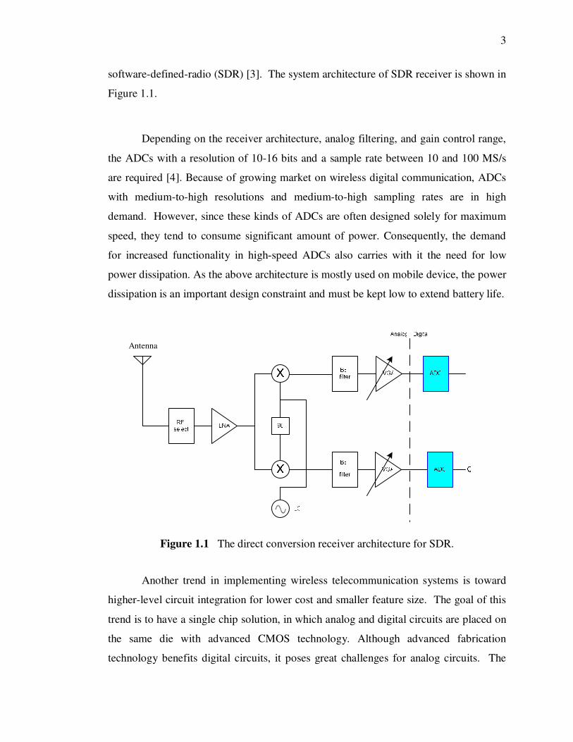
software-defined-radio (SDR) [3]. The system architecture of SDR receiver is shown in
Figure 1.1.
Depending on the receiver architecture, analog filtering, and gain control range,
the ADCs with a resolution of 10-16 bits and a sample rate between 10 and 100 MS/s
are required [4]. Because of growing market on wireless digital communication, ADCs
with medium-to-high resolutions and medium-to-high sampling rates are in high
demand. However, since these kinds of ADCs are often designed solely for maximum
speed, they tend to consume significant amount of power. Consequently, the demand
for increased functionality in high-speed ADCs also carries with it the need for low
power dissipation. As the above architecture is mostly used on mobile device, the power
dissipation is an important design constraint and must be kept low to extend battery life.
Figure 1.1 The direct conversion receiver architecture for SDR.
Another trend in implementing wireless telecommunication systems is toward
higher-level circuit integration for lower cost and smaller feature size. The goal of this
trend is to have a single chip solution, in which analog and digital circuits are placed on
the same die with advanced CMOS technology. Although advanced fabrication
technology benefits digital circuits, it poses great challenges for analog circuits. The
Antenna

4
scaling of CMOS devices degrades important analog performance. For instance,
lowering output resistance lowers amplifier gain, although cascading transistors or an
added gain stage can compensate for this lowered gain. However, the use of cascoding
transistors runs into a limitation on the number of transistors that can be stacked, a
limitation that is imposed by the low power supply voltage of scaled CMOS technology.
Turning to the solution of additional stages has the disadvantages of increased power
dissipation and more complicated circuitry.
The low power supply voltage of scaled CMOS technology also limits the
performance of analog circuits. Therefore, just as is the case with digital circuits,
simply lowering the power supply voltage in analog circuits does not necessarily result
in lower power dissipation. In addition, requirements for high gain and high speed
make it more difficult to lower their power consumption. This is especially true for
already complicated analog systems like ADCs; reducing their power consumption
requires careful analysis of system requirements and special strategies.
1.2 Problem Statement
Most modern communication devices are implemented on portable systems
powered by a battery with limited energy. Due to their dependence on batteries, some
efforts have to be made to minimize the power consumption of these devices. One of
the approaches is to use low power ADC. In this application, pipelined topology is the
most promising ADC architecture. Its properties are suited to the system requirement
that requires ADC with medium-to-high resolution and medium-to-high sampling rate.
The pipelined architecture also can be easily calibrated for higher resolution and has
potential for low voltage and low power operation. Thus, the objective of this work is
to design a low power 10-bit 50MS/s (Mega-Sample per-second) pipelined ADC for
wireless communication system applications.
5
1.3 Research Contribution
This research concentrates on pipelined ADC for wireless communication
system. Requirements and optimization of the pipelined ADCs, at the circuit and
architectural levels, are addressed to meet the specifications of this target application.
Although the proposed ADC is designed according to the specifications of the target
systems of wireless communication system, it can be exploited in other applications as
well. Based on this research work, some of the analysis and circuit implementations
have been partially reported in a related publication [5]. The contributions of this
research work are:
(i) Pipelined ADC MATLAB system model: MATLAB behavior models are
developed for the proposed pipelined ADC characterizations on its static
and dynamic linearity.
(ii) A low power 10-bit pipelined ADC architecture: Different architectures
on pipelined stages are investigated in order to determine the optimum
bit per stage structure in term of low power operation.
(iii) Transistor level pipelined ADC sub-circuits design and analysis: The
ADC sub-blocks such as amplifiers, comparators, non-overlapping clock
generator, switches, and digital error correction are designed and
simulated at circuit level.
(iv) Pipelined ADC layouts: The layout for 10-bit 50MS/s Pipelined ADC is
implemented using Siltera’s 0.18um CMOS process with double poly-
silicon and five metals technology. All techniques such as common-
centroid, cross-coupled, interdigitation, and IC decoupling are employed
in this layout to reduce parasitic effects.

6
1.4 Thesis Organization
The rest of the thesis is organized as follows. Chapter 2 presents the
literature review of ADCs and it is divided into three small sections. First,
Section 2.1 describes the importance of ADC performance parameters. Section
2.2 presents an overview of various ADC architectures. In section 2.3, the
pipelined ADC is presented in more details on its basic operation and sub-
blocks. Chapter 3 describes system architecture for the proposed pipelined ADC
as well as some analysis on its power optimization. Chapter 4 details the design
implementation of 10-bit 50MS/s pipelined ADC covering all its sub-
components including the amplifier, comparator, and digital error correction
circuit. Chapter 5 assesses the performance of the designed 10-bit 50MS/s
pipelined ADC. The thesis summary, research contribution, and direction for
future works are in Chapter 6.
79
REFERENCES
[1] B. Razavi. Design of Analog CMOS Integrated Circuits, McGraw-Hill. 2000
[2] S. Rapuano, P. Daponte, E. Balestrieri, L. De Vito, S. J. Tilden, S. Max, and J.
Blair. ADC parameters and characteristics. Instrumentation & Measurement
Magazine, vol.8, no.5, 2005. pp. 44-54.
[3] M. Sawan, A. Djemouai, K. El-Sankary, H. Dang, A. Naderi, Y. Savaria, and
F. Gagnon. High speed ADCs dedicated for wideband wireless receivers.
IEEE Northeast Workshop on Circuits and Systems (NEWCAS) Conference,
June 2005. Quebec, Canada. pp. 283-286
[4] L. Sumanen. Pipelined Analog-to-Digital for Wide-Band Wireless
Communications. Ph.D. Thesis. Helsinki University of Technology, Finland;
2002
[5] Y. Yusoff, R. Musa, N. Othman, M. S. Sulaiman and M. N. Marsono. A High-
Gain and High-Speed OTA for 10-bit 50MS/s Pipelined ADC. Student
Conference on Research and Development (SCORed), November 2008.
Skudai, Malaysia. Pp. 58-1-- 58-5.
[6] B. Razavi and B. A. Wooley. A 12-b, 5-Msample/s two-step CMOS A/D
converter. IEEE Journal of Solid-State Circuits. vol. 27, no.12, 1991. pp.
1667-1678.
[7] R. L. Geiger, P. E. Allen, N. R. Strader. VLSI Design Techniques for Analog
and Digital Circuits, McGraw Hill, 1990.
[8] M. Gustavsson, J. Jacob Wikner, and N. Nick Tan. CMOS Data Converters
for Communications, Kluwer Academic Publisher, 2000.

80
[9] T. Cho. Low-power Low-voltage Analog-to-Digital Conversion Technique
using Pipelined Architectures. Ph.D Thesis. University of California,
Berkeley; 1995.
[10] B. Nejati and 0. Shoaei. A 10-bit, 2.5-V, 40Msample/s, Pipelined Analog-to-
Digital Converter in 0.6-um CMOS. IEEE International Symposium on
Circuits and Systems. May, 2004. Vancouver, Canada. pp. I-73 -- I-76.
[11] H. Chen, B. Song and K. Bacrania. A 14-b 20-Msamples/s CMOS Pipelined
ADC. IEEE Journal Solid-State Circuits, vol. 36, no.6, 2001. pp. 997-1001.
[12] L. Williams and B. A. Wooley. A third-order sigma-delta modulation with
extended dynamic range,” IEEE Journal Solid-State Circuits, vol. 29, no. 3,
1994. pp. 193-202.
[13] B. P. Brandt, D. Wingard, and B. A. Wooley. Second-order sigma-delta
modulation for digital-audio signal acquisition. IEEE Journal on Solid-State
Circuits, vol. 26, no.4, 1991. pp.618-627.
[14] A. Reddy. Noise Shaping with Sigma Delta Modulators in Fractional-N
Synthesizers. IEEE International Workshop on Radio-Frequency Integration
Technology. December 2007, Singapore. pp. 329-332.
[15] J. Goes, J. C. Vital, J. E. Franca. A CMOS 4-bit MDAC with Self-
Calibrated14-bit Linearity for High-Resolution Pipelined A/D Converters.
Proceedings of the IEEE Custom Integrated Circuits Conference. May 1996,
San Diego, California. pp. 105-108.
[16] R. Gregorian, Introduction to CMOS Op-Amps and Comparators, John Wiley
and Sons. 1999.
[17] S. Kwak, B. Song, and K. Bacrania. A 15-b, 5-Msample/s Low-spurious
CMOS ADC. IEEE Journal Solid-State Circuits, vol. 32, no. 12, 1997. pp.
1866-1875.
[18] P. Allen and D. R. Holberg. CMOS Analog Circuit Design. 2nd
edition, Oxford
University Press, 2002.

81
[19] G. Nicollini, P. Confalonieri, D. Senderowicz. A Fully Differential Sample
and Hold Circuit for High-Speed Applications. IEEE Journal on Solid-State
Circuits, vol. 24, no. 5, 1989. pp. 1461–1465.
[20] K. Gulati and H. S. Lee. A High-Swing Telescopic Operational Amplifier.
IEEE Journal on Solid-State Circuits. vol. 33, no. 12, 1998. pp. 2010-2019.
[21] M.Yavari and O. Shoaei. Low-voltage Low-power Fast-settling CMOS
Operational Transconductance Amplifier for Switch Capacitor Applications.
IEEE Proceeding of Circuits, Devices and System, vol. 151, no. 6, 2004. pp.
573-578.
[22] B. Razavi, Principles of Data Conversion System Design, IEEE Press, 1995.
[23] N. Carter. A 12-b 50Msample/s Pipelined Analog to Digital Converter. MSc.
Thesis. Worcester Polytechnic Institute; 2000
[24] K. Kim, N. Kusayanagi, and A. Abidi. A 10-b, 100-MS/s CMOS A/D
Converter. IEEE Journal Solid-State Circuits. vol. 32, no.12, 1997. pp. 447-
454.
[25] S. H. Lewis. Optimizing the stage resolution in pipelined, multistage, analog-
to-digital converters for video-rate applications. IEEE Transaction on Circuits
and Systems-II. vol.39, no.8, 1992. pp. 516-523.
[26] P. T. F. Kwok and H. C. Luong. Power Optimization for Pipelined Analog-to-
Digital Converters. IEEE Transaction on Circuits and Systems-II. vol. 46, no.
5, 1999. pp. 549-553.
[27] D. Kelly, W. Yang, I. Mehr, M. Sayuk and L. Singer. A 3V 340mW 14b
75MSPS CMOS ADC with 85dB SFDR at Nyquist. IEEE International Solid-
State Circuit Conference Digest of Technical Papers. February 2001. pp. 134-
135.
[28] L. Reza, T. S. Mohd, M. Y. Azizi and O. Shoei. A Low-Power Design
Methodology for High-Resolution Pipelined Analog-to-Digital Converter.
Proceeding of International Symposium on Low Power Electronics and
Design. August 2003, Seoul, Korea. pp. 334-339.

82
[29] Y. Chiu. High-Performance Pipelined A/D Converter Design in Deep-
Submicron CMOS. Doctoral dissertation. University of California, Berkeley;
2004
[30] K. Bult, G. J. G. M. Geelen. A Fast-Settling CMOS Op Amp for SC Circuits
with 90-dB DC Gain. IEEE Journal Solid-State Circuits. vol. 25, no. 6, 1990.
pp. 1379-1384.
[31] P. C. Yu, H-S. Lee, A High-Swing 2-V CMOS Operational Amplifier with
Replica-Amp Gain Enhancement, IEEE Journal Solid-State Circuits. vol. 28,
no. 12, 1993. pp. 1265–1272.
[32] M. Das. Improved design criteria of gain-boosted CMOS OTA with high-
speed optimization. IEEE Transaction on Circuit and System-II. vol.49, no. 3,
2002. pp. 204-207
[33] A. M. Abo. Design for Reliability of Low-Voltage, Switched-capacitor
Circuits. Doctoral dissertation. University of California, Berkeley; 1999.
[34] M. Dessouky and A.Kaiser. Very low-voltage digital-audio Σ∆ modulator with
88-dB dynamic range using local switch bootstrapping. IEEE Journal Solid-
State Circuits. vol. 36, no. 3, 2001. pp. 349-355.
[35] A. Hasting. The Art of Analog Layout. Prentice-Hall, Inc. 2001
[36] J. Li, X. Zeng, J. Chen, J. Zhang, and Y. Guo. A 1.8-V 22mW 30MS/s
Subsampling Pipelined CMOS ADC. IEEE Custom Integrated Circuit
Conference. September, 2006. San Jose, California. pp. 513-516.
[37] W. Yang, D. Kelly, I. Mehr, M. Sayuk, and L.Singer. A 3-V 340mW 14-b
75Msample/s CMOS ADC with 85-dB SFDR at Nyquist Input. IEEE Journal
on Solid-State Circuits, vol.36, no12, 2001. pp. 1031-1936.
[38] I. Mehr, and L. Singer. A 55-mW, 10-bit, 40-Msample/s Nyquist-Rate CMOS
ADC. IEEE Journal on Solid-State Circuits, vol. 35, no. 3, March 2000. pp.
318-325.

83
[39] J. Talebzadeh, M. R. Hasanzadeh, M. Yavari, and O. Shoaei. A 10-bit 150-
MS/s, Parallel Pipelined A/D Converter in 0.6-um CMOS. Proceeding of
IEEE Symposium on Circuits and Systems. May 2002, Arizona, USA, pp. III-
(133-136).
[40] H. Liu, and M. Hassoun. A 9-b 40-MSample/s Reconfigurable Pipelined
Analog-to-Digital Converter. IEEE Journal on Solid-State Circuits, vol. 49,
no. 7, July 2002. pp. 449-456.
[41] M. Byung-Moo, P. Kim, F. W. Bowman, D. M. Boisvert, A. J. Aude. A 69-
mW 10-bit 80-MSample/s Pipelined CMOS ADC. IEEE Journal on Solid-
State Circuits, vol. 38, no. 12, December 2003. pp. 2031-2039.
[42] P. Jong-Bum, Y. Sang-Min, K. Se-Won, C. Young-Jae, and L. Seung-Hoon. A
10-b 150-MSample/s 1.8-V 123-mW CMOS A/D Converter with 400-MHz
Input Bandwidth. IEEE Journal on Solid-State Circuits, vol. 39, no. 8, August
2004. pp. 1335-1337.
[43] L. Jipeng, and Un-Ku Moon. A 1.8-V 67-mW 10-bit MS/s Pipelined ADC
Using Time-Shifted CDS Technique. IEEE Journal on Solid-State Circuits,
vol. 39, no. 9, September 2004. pp. 1468-1476.
[44] H. Mohamad-Faizal, Y. Yuzman, and M. Rais-Ahmad. A 10-bit 50-MSPS
Pipelined CMOS ADC. Proceeding of International Conference on
Semiconductor Electronics. Nov 2006, Kuala Lumpur, Malaysia. pp. 459-463.
[45] N. Sasidhar, K. Youn-Jae, S. Takeuchi, K. Hamashita, K. Takasuka, P. K.
Hanumolu, and Un-Ku Moon. A 1.8V 36-mW 11-bit MS/s Pipelined ADC
Using Capacitor and Opamp Sharing. IEEE Asian Solid-State Circuits
Conference, November 2007, Jeju, Korea. pp. 240-243.
[46] R. Seung-Tak , S. Bang-Sup, and K. Bacrania. A 10-bit 50-MS/s Pipelined
ADC With Opamp Current Reuse. IEEE Journal on Solid-State Circuits, vol.
42, no. 3, March 2007. pp. 475-485.
[47] J. Li, X. Zeng, L. Xie, J. Chen, J. Zhang, and Y. Guo. A 1.8-V 22-mW 10-bit
30MS/s Pipelined CMOS ADC for Low-Power Subsampling Applications.

84
IEEE Journal on Solid-State Circuits, vol. 43, no. 2, February 2008. pp. 321-
329.
[48] C. Junmin, C. Zhongjian, L. Wergao, and Z. Baoying. A Low Power 12-Bit 20
MSample/s Pipelined ADC. Proceeding of International Conference on Signal
Processing System. May 2009, Singapore.
[49] L. Jin-Fu, C. Soon-Jyh, L. Chun-Cheng, and H. Chih-Hao. A 10-bit 60-MS/s
Low-Power Pipelined ADC with Split-Capacitor CDS Technique. IEEE
Transactions on Circuits and Systems, vol. 57, no. 3, March 2010. pp. 163-
167.
[50] Y. Lai, Y. Xiumei, and Y. Huazhong. A 10-bit 100MSPS Low Power Time-
Interleaved ADC using OTA sharing. Journal of Semiconductor, vol. 31, no.9,
September 2010. pp. 095012-(1-6).