862 IEEE TRANSACTIONS ON VERY LARGE SCALE INTEGRATION...
13
862 IEEE TRANSACTIONS ON VERY LARGE SCALE INTEGRATION (VLSI) SYSTEMS, VOL. 21, NO. 5, MAY 2013 Study of Through-Silicon-Via Impact on the 3-D Stacked IC Layout Dae Hyun Kim, Student Member, IEEE, Krit Athikulwongse, Student Member, IEEE, and Sung Kyu Lim, Senior Member, IEEE Abstract— The technology of through-silicon vias (TSVs) enables fine-grained integration of multiple dies into a single 3-D stack. TSVs occupy significant silicon area due to their sheer size, which has a great effect on the quality of 3-D integrated chips (ICs). Whereas well-managed TSVs alleviate routing congestion and reduce wirelength, excessive or ill-managed TSVs increase the die area and wirelength. In this paper, we investigate the impact of the TSV on the quality of 3-D IC layouts. Two design schemes, namely TSV co-placement (irregular TSV placement) and TSV site (regular TSV placement), and accompanying algorithms to find and optimize locations of gates and TSVs are proposed for the design of 3-D ICs. Two TSV assignment algorithms are also proposed to enable the regular TSV place- ment. Simulation results show that the wirelength of 3-D ICs is shorter than that of 2-D ICs by up to 25%. Index Terms— 3-D integrated chip (IC), interconnect, place- ment, routing, through-silicon via (TSV). I. I NTRODUCTION 3 -D INTEGRATED CIRCUITS (3-D ICs) are emerging as a promising way to overcome interconnect scaling problems of 2-D ICs and improve performance further. In 3-D ICs, gates are placed in multiple dies, and the dies are stacked vertically on top of each other as illustrated in Fig. 1. Since gates are distributed in multiple dies, the footprint area of each die of a 3-D IC becomes smaller than that of the circuit designed in 2-D. A smaller footprint area results in shorter total wirelength in 3-D ICs than in 2-D ICs [1], [2]. Therefore, 3-D ICs have a high potential to improve the performance [3], [4]. Shorter wirelength can also reduce interconnect power and improve routing congestion. Less routing congestion can in turn reduce the number of metal layers used for routing in each die of a 3-D IC, and the reduction of the metal layer count can contribute to cost reduction [5]. Vertical interconnects across dies in 3-D ICs are enabled by via-first or via-last through-silicon vias (TSVs) as shown in Fig. 1. Typical diameters of via-first TSVs range from 1 to 5 μm and those of via-last TSVs range from 5 to Manuscript received September 26, 2011; revised February 22, 2012; accepted April 22, 2012. Date of publication August 14, 2012; date of current version April 22, 2013. This work was supported in part by the National Science Foundation under Grant CCF-1018216, Grant CCF-0917000, and Grant CCF-0546382. The authors are with the School of Electrical and Computer Engineer- ing, Georgia Institute of Technology, Atlanta, GA 30332 USA (e-mail: [email protected]; [email protected]; [email protected]). Color versions of one or more of the figures in this paper are available online at http://ieeexplore.ieee.org. Digital Object Identifier 10.1109/TVLSI.2012.2201760 via-first TSV via-last TSV top-down view of via-first TSV substrate substrate Fig. 1. Via-first and via-last TSVs with face-to-back bonding. 20 μm [6]–[10]. To connect TSVs and other gates, metal landing pads are attached to TSVs. Although TSVs play the most important role in gate-to-gate connections across dies, TSVs have negative impact on 3-D IC designs. Above all, TSVs are fabricated in bulk silicon, so they consume silicon area, which otherwise can be used for gates. In addition, keep-out-zone rules that forbid gate placement near TSVs must be satisfied. Because of these constraints and requirements, inserting excessive amount of TSVs into 3-D ICs can cause serious area overhead. In addition, TSVs consume routing resources because TSVs need to be routed to gates or other TSVs through metal layers. This might cause routing congestion. Therefore, CAD tools for the design of 3-D ICs should carefully account for the impact of TSVs during placement and routing. However, most previous works on CAD algorithms and tools for 3-D ICs, such as [11] and [12] ignore either the sheer size of TSVs or the fact that TSVs interfere with gates and/or wires. In this paper, the impact of TSVs on 3-D ICs is inves- tigated. This paper is based on design rules check (DRC)- clean GDSII layouts, and a complete set of simulation results are provided. The contributions of this paper are as follows. 1) Two 3-D IC design flows, namely “TSV co-placement design flow” and “TSV site design flow,” are proposed and compared. The TSV co-placement design scheme places TSVs and gates simultaneously, whereas the TSV site design scheme places TSVs at regular positions and then places gates. 2) Two TSV assignment algorithms for the TSV site scheme in which 3-D nets are assigned to pre-placed TSVs are developed. In addition, four TSV assign- ment algorithms are compared to investigate the impact 1063-8210/$31.00 © 2012 IEEE
Transcript of 862 IEEE TRANSACTIONS ON VERY LARGE SCALE INTEGRATION...

862 IEEE TRANSACTIONS ON VERY LARGE SCALE INTEGRATION (VLSI) SYSTEMS, VOL. 21, NO. 5, MAY 2013
Study of Through-Silicon-Via Impact onthe 3-D Stacked IC Layout
Dae Hyun Kim, Student Member, IEEE, Krit Athikulwongse, Student Member, IEEE,and Sung Kyu Lim, Senior Member, IEEE
Abstract— The technology of through-silicon vias (TSVs)enables fine-grained integration of multiple dies into a single 3-Dstack. TSVs occupy significant silicon area due to their sheer size,which has a great effect on the quality of 3-D integrated chips(ICs). Whereas well-managed TSVs alleviate routing congestionand reduce wirelength, excessive or ill-managed TSVs increasethe die area and wirelength. In this paper, we investigate theimpact of the TSV on the quality of 3-D IC layouts. Two designschemes, namely TSV co-placement (irregular TSV placement)and TSV site (regular TSV placement), and accompanyingalgorithms to find and optimize locations of gates and TSVsare proposed for the design of 3-D ICs. Two TSV assignmentalgorithms are also proposed to enable the regular TSV place-ment. Simulation results show that the wirelength of 3-D ICs isshorter than that of 2-D ICs by up to 25%.
Index Terms— 3-D integrated chip (IC), interconnect, place-ment, routing, through-silicon via (TSV).
I. INTRODUCTION
3 -D INTEGRATED CIRCUITS (3-D ICs) are emergingas a promising way to overcome interconnect scaling
problems of 2-D ICs and improve performance further. In3-D ICs, gates are placed in multiple dies, and the diesare stacked vertically on top of each other as illustratedin Fig. 1. Since gates are distributed in multiple dies, thefootprint area of each die of a 3-D IC becomes smaller thanthat of the circuit designed in 2-D. A smaller footprint arearesults in shorter total wirelength in 3-D ICs than in 2-DICs [1], [2]. Therefore, 3-D ICs have a high potential toimprove the performance [3], [4]. Shorter wirelength can alsoreduce interconnect power and improve routing congestion.Less routing congestion can in turn reduce the number ofmetal layers used for routing in each die of a 3-D IC, andthe reduction of the metal layer count can contribute to costreduction [5].
Vertical interconnects across dies in 3-D ICs are enabledby via-first or via-last through-silicon vias (TSVs) as shownin Fig. 1. Typical diameters of via-first TSVs range from1 to 5 μm and those of via-last TSVs range from 5 to
Manuscript received September 26, 2011; revised February 22, 2012;accepted April 22, 2012. Date of publication August 14, 2012; date of currentversion April 22, 2013. This work was supported in part by the NationalScience Foundation under Grant CCF-1018216, Grant CCF-0917000, andGrant CCF-0546382.
The authors are with the School of Electrical and Computer Engineer-ing, Georgia Institute of Technology, Atlanta, GA 30332 USA (e-mail:[email protected]; [email protected]; [email protected]).
Color versions of one or more of the figures in this paper are availableonline at http://ieeexplore.ieee.org.
Digital Object Identifier 10.1109/TVLSI.2012.2201760
via-first TSV via-last TSV top-down view of via-first TSV
substrate substrate
Fig. 1. Via-first and via-last TSVs with face-to-back bonding.
20 μm [6]–[10]. To connect TSVs and other gates, metallanding pads are attached to TSVs.
Although TSVs play the most important role in gate-to-gateconnections across dies, TSVs have negative impact on 3-D ICdesigns. Above all, TSVs are fabricated in bulk silicon, so theyconsume silicon area, which otherwise can be used for gates.In addition, keep-out-zone rules that forbid gate placementnear TSVs must be satisfied. Because of these constraintsand requirements, inserting excessive amount of TSVs into3-D ICs can cause serious area overhead. In addition, TSVsconsume routing resources because TSVs need to be routed togates or other TSVs through metal layers. This might causerouting congestion. Therefore, CAD tools for the design of3-D ICs should carefully account for the impact of TSVsduring placement and routing. However, most previous workson CAD algorithms and tools for 3-D ICs, such as [11] and[12] ignore either the sheer size of TSVs or the fact that TSVsinterfere with gates and/or wires.
In this paper, the impact of TSVs on 3-D ICs is inves-tigated. This paper is based on design rules check (DRC)-clean GDSII layouts, and a complete set of simulationresults are provided. The contributions of this paper are asfollows.
1) Two 3-D IC design flows, namely “TSV co-placementdesign flow” and “TSV site design flow,” are proposedand compared. The TSV co-placement design schemeplaces TSVs and gates simultaneously, whereas the TSVsite design scheme places TSVs at regular positions andthen places gates.
2) Two TSV assignment algorithms for the TSV sitescheme in which 3-D nets are assigned to pre-placedTSVs are developed. In addition, four TSV assign-ment algorithms are compared to investigate the impact
1063-8210/$31.00 © 2012 IEEE

KIM et al.: STUDY OF TSV IMPACT ON THE 3-D STACKED IC LAYOUT 863
TABLE I
ASSUMPTIONS, PARAMETERS, AND TERMINOLOGIES
USED IN THIS PAPER
Value/Meaning
Process technology 45nm
Die bonding face-to-back
TSV shape square
TSV type via-first
TSV size (n×) small (1×), medium (2×), large (3×)
n× TSV width n · 1.50 μm (n = 1, 2, or 3)
n× TSV landing pad width n · 2.07 μm (n = 1, 2, or 3)
n× TSV cell width n · 2.47 μm (n = 1, 2, or 3)
Min. TSV-to-cell spacing n · 0.4 μm for n× TSV
Min. TSV-to-TSV spacing n · 0.8 μm for n× TSV
TSV resistance (1× TSV) 100 m�
TSV capacitance (1× TSV) 5 fF
2-D net a net whose cells exist in a single die
3-D net a net whose cells exist across multiple dies
of the quality of TSV assignment algorithms on thewirelength.
3) Since TSVs have negative effects, such as occupyingsilicon area, various layouts are generated and comparedto show the impact of TSVs on wirelength and area of3-D ICs.
The rest of this paper is organized as follows. In Section II,preliminary studies on 3-D ICs and TSVs are presented.In Section III, two 3-D IC design schemes are introduced.The 3-D placement algorithm is explained in Section IV. InSection V, the TSV assignment algorithms are developed.Simulation results are shown in Section VI, and conclusionsare provided in Section VII.
II. PRELIMINARIES
In this section, previous works are discussed, and designissues, such as 3-D placement and 3-D DRC are introducedand explained. Then the impact of TSV count on die area isaddressed. Table I lists assumptions, parameters, and termi-nologies used in this paper.
A. Previous Works
Several placement algorithms for the design of 3-D ICs havebeen proposed in the literature. In [13], the authors randomlyplace standard cells within the placement area, and use forcesto move the cells in three dimensions to reduce cell overlap andtemperature. In [11], the authors transform a 2-D placementresult into 3-D. The proposed transformations are based onfolding and stacking a 2-D design. After the transformation,they use a graph-based layer assignment method to refine the3-D placement result by placing cells into multiple layers toreduce the number of TSVs and temperature.
Reference [12] proposes analytical and partitioning-basedtechniques for placement of 3-D ICs. A recursive bisectionapproach is used during global placement, and the cut directionfor each bisection is selected as orthogonal to the largest ofthe width, height, or weighted depth of the placement area.
metal layers
TSV landing padssilicon bulk
TSV
die
ndi
e n+
1 M2M1
Mtop
M3M2M1
Fig. 2. TSVs, TSV landing pads, and connections to TSV landing pads.
wire-to-TSV
wire-to-TSV
(a) (b)
M1 landing padM6 landing pad
Fig. 3. TSV landing pads (yellow) and metal wires (M1 in blue and M6 inred) connected to the landing pads (Cadence Virtuoso). (a) Landing pad inM1. (b) Landing pad in M6.
In [14], the authors propose a multilevel nonlinearprogramming-based placement algorithm for 3-D ICs. Theirobjective is the weighted sum of wirelength and the numberof TSVs. The authors use a density penalty function toremove overlap. They also use a bell-shaped density projectionfunction helps to obtain a legal placement in the z-direction.
Reference [13] does not consider the TSV at all in any stage.Although [11], [12], and [14] consider the number of TSVs,all the placement algorithms do not account for TSV area.
Since the initial work of this paper was published in[15], [16], and [17] proposed different 3-D placement andTSV insertion algorithms. [16] performs global placement byiterative partitioning and then inserts TSVs. On the other hand,[17] performs global placement by analytical placement, whichdetermines the number of TSVs. The wirelength of [17] isbetter than that of [15]. However, the 3-D global placer usedin this paper is an improved version of the 3-D global placerused in [15], and the wirelength comparison presented in theappendix shows that the 3-D global placer of this paper isbetter than those of [15] and [17].
B. Design of 3-D ICs
In 3-D ICs, gates and TSVs are placed in multiple dies.Since both TSVs and gates occupy silicon area, overlapsbetween them should be avoided. In addition, TSVs shouldbe routed without violating design rules. Fig. 2 illustratesconnections to TSVs. Since a TSV is in fact connected to itsM1 landing pad in the same die and Mtop landing pad in thebottom die (or backside landing pad in the same die), wires tothese landing pads for connections to TSVs are routed. Fig. 3shows landing pads in M1 and M6 (=Mtop) and the wires
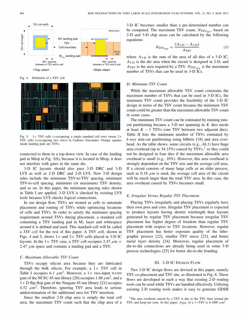
864 IEEE TRANSACTIONS ON VERY LARGE SCALE INTEGRATION (VLSI) SYSTEMS, VOL. 21, NO. 5, MAY 2013
Fig. 4. Definition of a TSV cell.
Fig. 5. 1× TSV cells (=occupying a single standard cell row) versus 2×TSV cells (=occupying two rows) in Cadence Encounter. Orange squaresinside landing pads are TSVs.
connected to them in a top-down view. In case of the landingpad in Mtop in Fig. 3(b), because it is located in Mtop, it doesnot interfere with gates in the same die.
3-D IC layouts should also pass 3-D DRC and 3-DLVS as well as 2-D DRC and 2-D LVS. New 3-D designrules include the minimum TSV-to-TSV spacing, minimumTSV-to-cell spacing, minimum (or maximum) TSV density,and so on. In this paper, the minimum spacing rules shownin Table I are applied. 3-D LVS is checked by existing LVStools because LVS checks logical connections.
In our design flow, TSVs are treated as cells to automateplacement and routing of TSVs while optimizing locationsof cells and TSVs. In order to satisfy the minimum spacingrequirement around TSVs during placement, a standard cellcontaining a TSV landing pad in M1 layer and whitespacearound it is defined and used. This standard cell will be calleda TSV cell for the rest of this paper. A TSV cell, shown inFigs. 4 and 5, shows 1× and 2× TSV cells placed in 3-D IClayouts. In the 1× TSV case, a TSV cell occupies 2.47 μm ×2.47 μm space and contains a landing pad and a TSV.
C. Maximum Allowable TSV Count
TSVs occupy silicon area because they are fabricatedthrough the bulk silicon. For example, a 1× TSV cell inTable I occupies 6.1 μm2. However, a 1× two-input NAND
gate of the NCSU 45-nm library [20] occupies 1.88 μm2, and a1× D flip-flop gate of the Nangate 45-nm library [21] occupies4.52 μm2. Therefore, ignoring TSV area leads to seriousunderestimation of the additional area for TSV insertion.
Since the smallest 2-D chip area is simply the total cellarea, the maximum TSV count such that the chip area of a
3-D IC becomes smaller than a pre-determined number canbe computed. The maximum TSV count, NTSVmax , based on2-D and 3-D chip areas can be calculated by the followingequations:
NTSVmax = (A3-D − A2-D)
ATSV(1)
where A3-D is the sum of the area of all dies of a 3-D IC,A2-D is the die area when the circuit is designed in 2-D, andATSV is the area required by a TSV. NTSVmax is the maximumnumber of TSVs that can be used in 3-D ICs.
D. Minimum TSV Count
While the maximum allowable TSV count constrains themaximum number of TSVs that can be used in 3-D ICs, theminimum TSV count provides the feasibility of the 3-D ICdesign in terms of the TSV count because the minimum TSVcount could be greater than the maximum allowable TSV countin some cases.
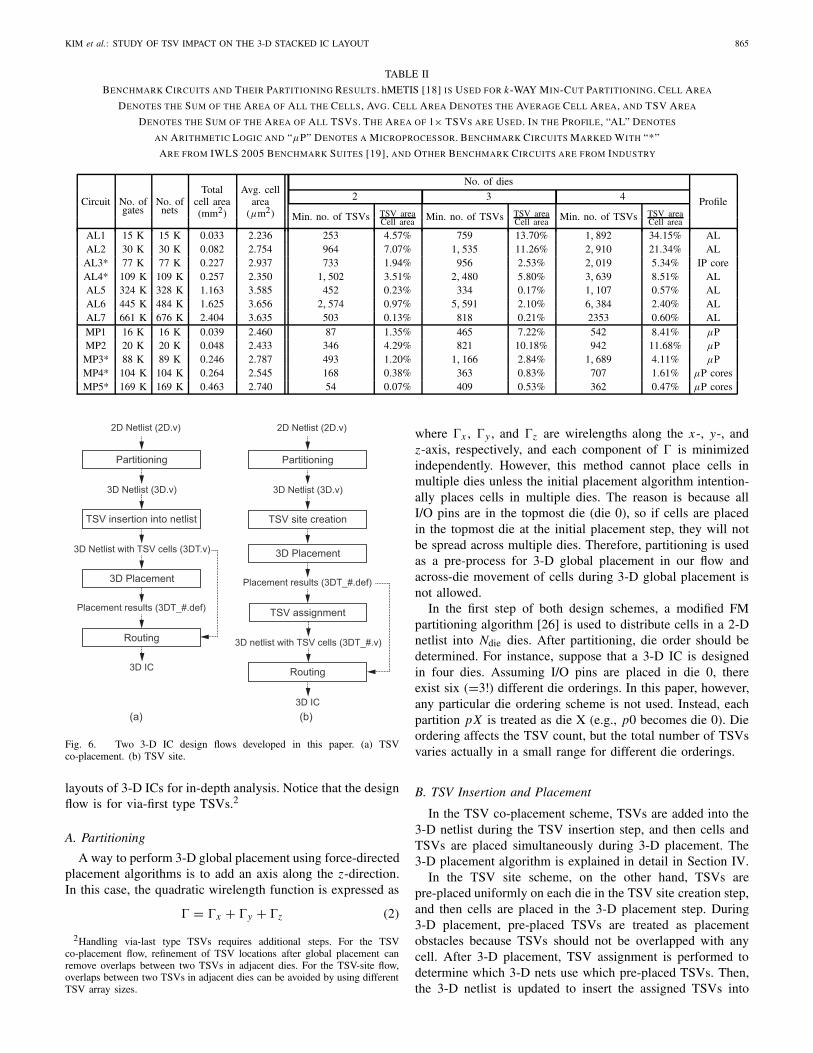
The minimum TSV count can be estimated by running min-cut partitioning because a 3-D net spanning in K dies needsat least K − 1 TSVs (one TSV between two adjacent dies).Table II lists the minimum number of TSVs estimated byk-way min-cut partitioning using hMetis [18] and area over-head. As the table shows, some circuits (e.g., AL1) have hugearea overhead (up to 34.15%) caused by TSVs,1 so they couldnot be designed in four dies if the maximum allowable areaoverhead is small (e.g., 10%). However, this area overhead isstrongly dependent on the TSV size and the average cell area.If a circuit consists of many large cells or an older process,such as 0.18 μm is used, the average cell area of the circuitwill be much larger than the total TSV area. In this case, thearea overhead caused by TSVs becomes small.
E. Irregular Versus Regular TSV Placement
Placing TSVs irregularly and placing TSVs regularly havetheir own pros and cons. Irregular TSV placement is expectedto produce layouts having shorter wirelength than layoutsgenerated by regular TSV placement because irregular TSVplacement has higher degree of freedom than regular TSVplacement with respect to TSV locations. However, regularTSV placement has better exposure quality of the litho-graphic process [22], smaller TSV stress [23], and bettermetal layer density [24]. Moreover, regular placement ofdie-to-die connections are already being used in some 3-Dprocess technologies [25] for better die-to-die bonding.
III. 3-D IC DESIGN FLOW
Two 3-D IC design flows are devised in this paper, namelyTSV co-placement and TSV site, as illustrated in Fig. 6. Theseflows are developed in such a way that existing 2-D routingtools can be used while TSVs are handled effectively. Utilizingexisting 2-D routing tools makes it easy to generate GDSII
1The area overhead caused by a TSV is due to the TSV, liner around theTSV, and keep-out zone. In this paper, ATSV of a 1×TSV is 6.1009 μm2.
KIM et al.: STUDY OF TSV IMPACT ON THE 3-D STACKED IC LAYOUT 865
TABLE II
BENCHMARK CIRCUITS AND THEIR PARTITIONING RESULTS. hMETIS [18] IS USED FOR k-WAY MIN-CUT PARTITIONING. CELL AREA
DENOTES THE SUM OF THE AREA OF ALL THE CELLS, AVG. CELL AREA DENOTES THE AVERAGE CELL AREA, AND TSV AREA
DENOTES THE SUM OF THE AREA OF ALL TSVS. THE AREA OF 1× TSVS ARE USED. IN THE PROFILE, “AL” DENOTES
AN ARITHMETIC LOGIC AND “μP” DENOTES A MICROPROCESSOR. BENCHMARK CIRCUITS MARKED WITH “*”
ARE FROM IWLS 2005 BENCHMARK SUITES [19], AND OTHER BENCHMARK CIRCUITS ARE FROM INDUSTRY
Circuit No. of No. ofTotal
cell area(mm2)
Avg. cellarea
(μm2)
No. of dies
Profile2 3 4gates nets
Min. no. of TSVs TSV areaCell area Min. no. of TSVs TSV area
Cell area Min. no. of TSVs TSV areaCell area
AL1 15 K 15 K 0.033 2.236 253 4.57% 759 13.70% 1, 892 34.15% ALAL2 30 K 30 K 0.082 2.754 964 7.07% 1, 535 11.26% 2, 910 21.34% AL
AL3* 77 K 77 K 0.227 2.937 733 1.94% 956 2.53% 2, 019 5.34% IP coreAL4* 109 K 109 K 0.257 2.350 1, 502 3.51% 2, 480 5.80% 3, 639 8.51% ALAL5 324 K 328 K 1.163 3.585 452 0.23% 334 0.17% 1, 107 0.57% ALAL6 445 K 484 K 1.625 3.656 2, 574 0.97% 5, 591 2.10% 6, 384 2.40% ALAL7 661 K 676 K 2.404 3.635 503 0.13% 818 0.21% 2353 0.60% ALMP1 16 K 16 K 0.039 2.460 87 1.35% 465 7.22% 542 8.41% μPMP2 20 K 20 K 0.048 2.433 346 4.29% 821 10.18% 942 11.68% μPMP3* 88 K 89 K 0.246 2.787 493 1.20% 1, 166 2.84% 1, 689 4.11% μPMP4* 104 K 104 K 0.264 2.545 168 0.38% 363 0.83% 707 1.61% μP coresMP5* 169 K 169 K 0.463 2.740 54 0.07% 409 0.53% 362 0.47% μP cores
2D Netlist (2D.v)
Partitioning
3D Netlist (3D.v)
TSV insertion into netlist
3D Netlist with TSV cells (3DT.v)
3D Placement
Placement results (3DT_#.def)
Routing
3D IC
(a) (b)
2D Netlist (2D.v)
Partitioning
3D Netlist (3D.v)
TSV site creation
3D Placement
Placement results (3DT_#.def)
Routing
3D IC
TSV assignment
3D netlist with TSV cells (3DT_#.v)
Fig. 6. Two 3-D IC design flows developed in this paper. (a) TSVco-placement. (b) TSV site.
layouts of 3-D ICs for in-depth analysis. Notice that the designflow is for via-first type TSVs.2
A. Partitioning
A way to perform 3-D global placement using force-directedplacement algorithms is to add an axis along the z-direction.In this case, the quadratic wirelength function is expressed as
� = �x + �y + �z (2)
2Handling via-last type TSVs requires additional steps. For the TSVco-placement flow, refinement of TSV locations after global placement canremove overlaps between two TSVs in adjacent dies. For the TSV-site flow,overlaps between two TSVs in adjacent dies can be avoided by using differentTSV array sizes.
where �x , �y , and �z are wirelengths along the x-, y-, andz-axis, respectively, and each component of � is minimizedindependently. However, this method cannot place cells inmultiple dies unless the initial placement algorithm intention-ally places cells in multiple dies. The reason is because allI/O pins are in the topmost die (die 0), so if cells are placedin the topmost die at the initial placement step, they will notbe spread across multiple dies. Therefore, partitioning is usedas a pre-process for 3-D global placement in our flow andacross-die movement of cells during 3-D global placement isnot allowed.
In the first step of both design schemes, a modified FMpartitioning algorithm [26] is used to distribute cells in a 2-Dnetlist into Ndie dies. After partitioning, die order should bedetermined. For instance, suppose that a 3-D IC is designedin four dies. Assuming I/O pins are placed in die 0, thereexist six (=3!) different die orderings. In this paper, however,any particular die ordering scheme is not used. Instead, eachpartition pX is treated as die X (e.g., p0 becomes die 0). Dieordering affects the TSV count, but the total number of TSVsvaries actually in a small range for different die orderings.
B. TSV Insertion and Placement
In the TSV co-placement scheme, TSVs are added into the3-D netlist during the TSV insertion step, and then cells andTSVs are placed simultaneously during 3-D placement. The3-D placement algorithm is explained in detail in Section IV.
In the TSV site scheme, on the other hand, TSVs arepre-placed uniformly on each die in the TSV site creation step,and then cells are placed in the 3-D placement step. During3-D placement, pre-placed TSVs are treated as placementobstacles because TSVs should not be overlapped with anycell. After 3-D placement, TSV assignment is performed todetermine which 3-D nets use which pre-placed TSVs. Then,the 3-D netlist is updated to insert the assigned TSVs into

866 IEEE TRANSACTIONS ON VERY LARGE SCALE INTEGRATION (VLSI) SYSTEMS, VOL. 21, NO. 5, MAY 2013
Fig. 7. TSV insertion, 3-D placement, TSV assignment, and netlist generation.
the netlist. Fig. 7 illustrates the TSV co-placement and TSVsite schemes. For detailed placement, the detailed placer ofCadence system-on-chip Encounter is used [27].
C. Routing
After 3-D placement, the placement result is dumped intoDEF files and a netlist file is generated for each die. At thistime, TSV landing pads should be made at both ends of aTSV as shown in Fig. 2. While an M1 landing pad is placedin die(n + 1), its corresponding MTOP landing pad is placedin die(n) at the same location. An MTOP landing pad in die(n)is represented by placing a pin in the DEF file of die(n) andadding the pin into the netlist of die(n). Then, Encounter isused to route each die.
IV. 3-D GLOBAL PLACEMENT ALGORITHM
The 3-D global placement algorithm used in this paper isbased on a force-directed quadratic placement algorithm [28].The algorithm is modified to place cells and TSVs in 3-D.
A. Overview of Force-Directed Quadratic Placement
In quadratic placement, optimal locations of cells arecomputed by minimizing the quadratic wirelength function �,expressed as
� = �x + �y (3)
where �x and �y are wirelengths along the x- and y-axis.�x is written as
�x = 1
2xTCxx + xTdx + constant (4)
where x represents the x-position of N cells, Cx is an N × Nconnectivity matrix using the bound-to-bound net model [28],and dx represents the connectivity between cells and pins.Element cx,i j of Cx is the weight of the connection betweencell i and cell j , and element dx,i is the negative weightedposition of the fixed pins connected to cell i . �x is minimizedby solving the following equations:
∇x�x = Cx x + dx = 0. (5)
Quadratic placement can be viewed as an elastic springsystem when � is treated as the total spring energy of thesystem. Because the derivative of the spring energy is a force,the derivative of �x in (4) can be viewed as a net force fnet
x as
fnetx = ∇x�x = Cxx + dx (6)
where ∇x is the vector differential operator. At equilibrium,fnetx is zero and �x is minimized, which results in overlaps
among cells. To remove cell overlap, [28] uses two additionalforces, the move force fmove
x and the hold force fholdx .
The move force is a density-based force that spreads cellsaway from high cell density area to low cell density area toreduce cell overlap. The move force in [28] is defined for 2-DICs, thus it is modified to lower cell densities in 3-D ICs. Themodification is explained in Section IV-C.
The hold force is used to decouple each placement iterationfrom its previous iteration. It cancels out the net force thatpulls cells back to the location in the previous iteration. Thehold force is written as
fholdx = −(Cxx′ + dx) (7)
where x′ contains the x-position of cells from the previousplacement iteration. When no move force is applied, the holdforce holds cells at their current locations.
The total force fx is the summation of the net force, moveforce, and hold force. The total force is set to zero to minimizewirelength while removing cell overlap.
B. Overview of Our 3-D Placement Algorithm
The proposed 3-D placement algorithm is divided intothree phases: initial placement, global placement, and detailedplacement. In the first phase, the initial cell locations arecomputed by solving (5). In the second phase, the amountof cell overlaps is reduced by applying the move force andthe hold force included in solving the equation. Overlapsare removed gradually because moving cells rapidly degradesthe overall placement quality. Global placement continuesuntil the amount of remaining cell overlap becomes lower

KIM et al.: STUDY OF TSV IMPACT ON THE 3-D STACKED IC LAYOUT 867
than a pre-determined overlap ratio. Then detailed placementis performed using the detailed placer included in Cadenceencounter.
C. Cell Placement in 3-D ICs
A major extension on the 2-D force-directed quadraticplacement algorithm in this paper is to modify the move forcein [28] so that removing cell overlap is performed in eachdie separately. For example, the move force is not appliedbetween two cells at the same x and y location if they are indifferent dies.
The placement problem is formulated as a global electrosta-tic problem, by treating cell area as positive charge and chiparea as negative charge. The placement density D on die dcan be computed by
D(x, y)∣∣∣z=d
= Dcell(x, y)∣∣∣z=d
− Dchip(x, y)∣∣∣z=d
(8)
where Dcell(x, y)∣∣z=d is the cell density at position (x, y) in
die d , and Dchip(x, y)∣∣z=d is the chip capacity at position
(x, y) in die d .After D is computed, the following Poission’s equation is
solved to compute the placement potential � as follows:
��(x, y)∣∣∣z=d
= −D(x, y)∣∣∣z=d
. (9)
The move force is modeled by connecting cell i to its targetpoint xi with a spring of spring constant wi . The target pointis computed by
xi = x ′i − ∂
∂x�(x, y)
∣∣∣(x ′
i ,y′i ),z=d
(10)
where x ′i is the x-position of cell i being placed on die d in the
previous placement iteration. The spring constant is initiallydefined by
wi = Ai
Acell∣∣z=d
(11)
where Ai is the area of cell i , and Acell∣∣z=d is total area
of cells being placed on die d . Then, the spring constantis adjusted iteratively using the quality control mechanismin [28]. Therefore, for cell i , the move force is f move
x,i =wi (xi − xi ), where xi is the x-position of cell i . The moveforce fmove
x is finally defined for 3-D ICs by
fmovex = Cx (x − x) (12)
where Cx is a diagonal matrix of wi , x is a vector representingthe x-position of N cells being placed, and x is a vectorrepresenting the target x-position of the cells.
D. Pre-Placement of TSVs in TSV Site Scheme
In the TSV site scheme, TSVs are placed evenly and thencells are placed. Therefore, TSVs are treated as placementobstacles during cell placement. The number of TSVs in eachrow and column is computed by
NTSVd = NTSVd,min × KTSV KTSV ≥ 1 (13)
NTSVd,row = �√NTSVd � (14)
NTSVd,col =⌈
NTSVd
NTSVd,row
⌉
(15)
where NTSVd,min is the minimum number of TSVs on die d ,and KTSV is a multiplying factor for the number of TSVs.If KTSV is greater than one, more TSVs than the minimumTSV count are placed to increase the selectivity during TSVassignment.
Placement obstacles can be handled naturally by means ofthe placement density in [28]. By including the area of pre-placed TSVs in the computation of the placement density, themove force is altered in such a way that it moves cells beingplaced away from pre-placed TSVs. The area of pre-placedTSVs is also included in (8).
V. TSV ASSIGNMENT
The TSV assignment problem in the TSV site scheme is toassign 3-D nets to TSVs for given sets of dies, 3-D nets, placedcells, and placed TSVs while optimizing objective functions,such as the total wirelength of the 3-D nets. Constraints in theTSV assignment problem are as follows:
1) a TSV cannot be assigned to more than one 3-D net;2) a 3-D net should use at least one TSV.
A. Optimum Solution for TSV Assignment
The authors of [29] show the binary integer linear pro-gramming (BILP) formulation to find the optimum solutionof the TSV assignment problem for two dies. Since thenumber of binary integer variables in the formula is toobig, they also introduce and develop heuristic algorithms, anapproximation method based on the Hungarian method [30],and a neighborhood search method.
If a 3-D IC is designed in more than two dies and a3-D net spans more than two dies, all the combinationsof TSVs in different dies should be taken into account forthe cost computation. In Fig. 8(a), for example, the 3-Dnet is assigned to T1 in die 1 and T6 in die 2, and thecost (=wirelength) is approximately 2L. However, in Fig. 8(b),the 3-D net is assigned to T3 in die 1 and T6 in die 2, andthe cost is approximately L. Although T6 is used in bothcases, its contribution to the cost is different. Therefore, thecost should be computed for each combination of TSVs indifferent dies.
The optimum solution for a TSV assignment problem formore than two dies is found by the following formulation:min
N3-DNet∑
i=1
C Bi∑
k=1
NTSV∑
p=1
di,k,p · xi,k,p (16)
s.tC Bi∑
k=1
NTSV∑
p=1
xi,k,p = Ndie−1 (i = 1, . . . , N3-DNet) (17)
N3-DNet∑
i=1
C Bi∑
k=1
xi,k,p ≤ 1 (p = 1, . . . , NTSV) (18)
where Ndie is the number of dies, N3-DNet is the total numberof 3-D nets, C Bi is the total number of combinations ofTSVs for the 3-D net Hi , NTSV is the total number of
868 IEEE TRANSACTIONS ON VERY LARGE SCALE INTEGRATION (VLSI) SYSTEMS, VOL. 21, NO. 5, MAY 2013
Fig. 8. Cost computation for different combinations of TSVs in threedies (side view). (a) Wirelength = 2L when T1 and T6 are selected.(b) Wirelength = L when T3 and T6 are selected.
TSVs, and di,k,p is the cost when the pth TSV in thekth combination is used for the 3-D net Hi . Here, xi,k,p is 1if: 1) the 3-D net Hi uses the kth combination and 2) the kthcombination uses the TSV Tp, is 0 otherwise. Equation (17)denotes that a 3-D net uses only one combination of TSVsand (18) denotes that a TSV is assigned to at most one3-D net.
The number of variables in this problem is also verylarge. Even if TSVs available for a 3-D net are limitedto TSVs inside a small window, the number of combina-tions is still large. For example, if a 3-D net spans infour dies, and the window contains 20 TSVs in each die,8000 combinations exist for the net. Moreover, restriction onthe window size may result in infeasibility of BILP. There-fore, two heuristic algorithms are proposed in the next twosections.
B. Minimum Spanning Tree (MST)-Based TSV Assignment
In this method, the MST algorithm is used for TSV assign-ment as shown in Algorithm 1. First, 3-D nets are sorted in theascending order of their bounding box size. Since a 3-D netwhose bounding box is large contains more TSVs to choosefrom, higher priority is given to 3-D nets having smallerbounding boxes. After sorting, an MST is constructed usingKruskal’s algorithm for each 3-D net, and the edges of theMST are sorted in the ascending order of their lengths becausea short edge means short wirelength. After constructing theMST and sorting edges, each edge is checked in the ascendingorder. If the edge spans over two adjacent dies that are not con-nected yet, the unassigned TSV closest to the edge is chosenand marked as “assigned to this net.” This process is repeateduntil all dies in the 3-D net are connected by TSVs. Duringthis assignment process, the distance between an availableTSV and a 3-D edge is computed as follows. The edge isprojected to a 2-D plane so that the 3-D edge becomes a 2-Dsegment. Then, the distance is computed by calculating theManhattan distance between the TSV and its nearest point inthe segment.
An example is shown in Fig. 9. The shortest edge in thefigure is the vertical edge connecting dies 1 and 2. Theavailable TSV closest to the edge is T3, so it is assigned to the3-D net. Since this 3-D net spans from die 1 to die 3, a TSVin die 2 is needed to connect cells in die 2 and die 3. TheTSV closest to the next shortest edge is T6. Since this is an
Algorithm 1 MST-Based TSV Assignment1: Sort 3-D nets in the order of bounding box size2: for each 3-D net (Hi ) do3: construct an MST (Kruskal’s algorithm)4: sort edges in the ascending order of edge length5: for each edge (e j ) do6: if this e j connects two dies already connected then7: continue;8: end if9: find the TSV nearest to e j in the same die
10: assign this TSV to Hi
11: if all dies are connected then12: break;13: end if14: end for15: end for
Cell Available TSV Non-available TSV
Die 1Die 2Die 3
T1 T2 T3
T4 T5 T6
T1 T2 T3
T4 T5 T6
Fig. 9. Example: MST-based TSV assignment (side view).
unavailable TSV, which means it has already been assigned toanother net, the next closest TSV, T5 is found and assigned.
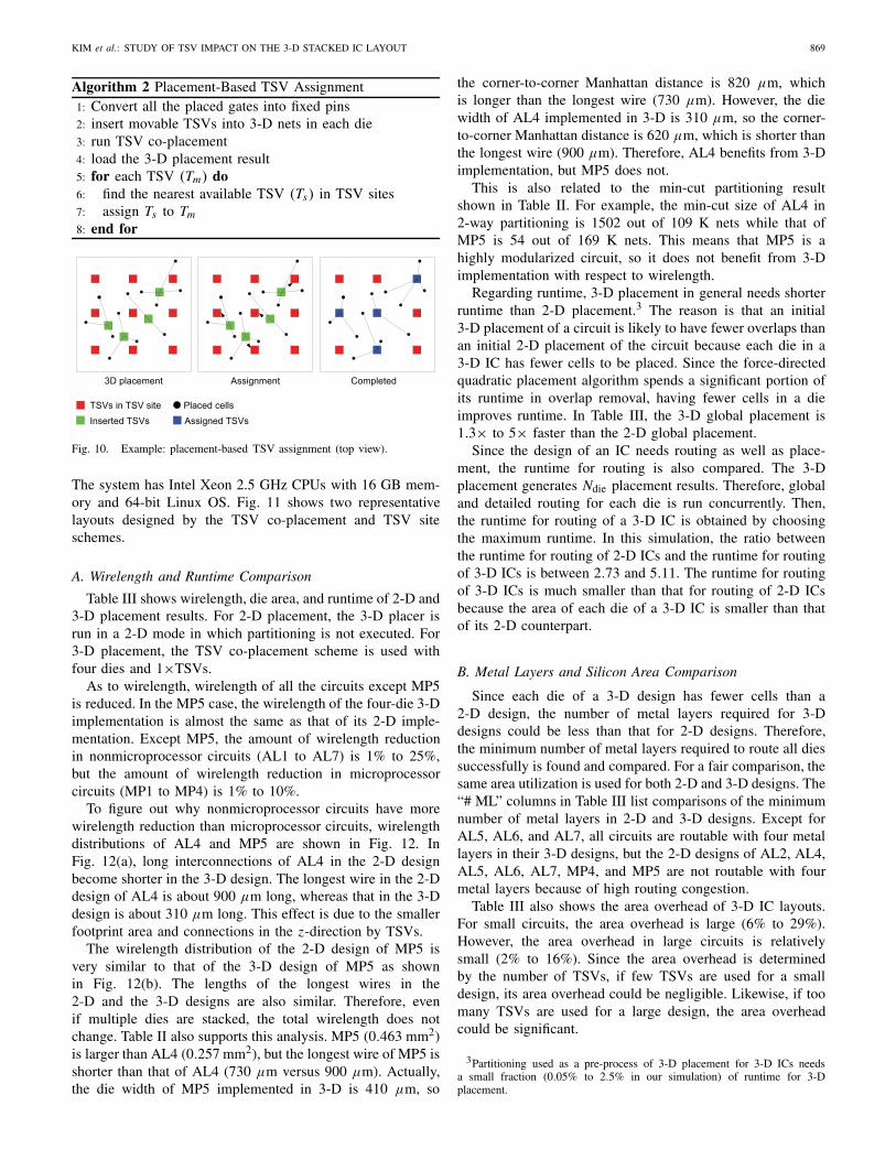
C. Placement-Based TSV Assignment
The second TSV assignment method is based on 3-Dplacement. In this method, the the assignment problem issolved by a 3-D placement algorithm. Algorithm 2 shows theplacement-based TSV assignment algorithm.
After placing gates in the 3-D placement stage, the placedgates are converted into pins in a new 3-D netlist. There-fore, there exist only pins, which are actually I/O pins andplaced gates, in the netlist. Then, movable TSVs are insertedinto this netlist, and TSV co-placement is performed. Afterplacement is finished, TSV locations are loaded from the 3-Dplacement result. At this time, however, the TSVs inserted inthe netlist are assigned to pre-placed TSVs. Fig. 10 shows anexample. In the first step, movable TSVs (gray squares) areinserted into a new netlist and placed by the 3-D placementalgorithm. After 3-D placement, the final locations of themovable TSVs are assigned to their nearest pre-placed TSVs.The final assignment result is shown in the rightmost figureof Fig. 10.
VI. SIMULATION RESULTS
IWLS 2005 benchmarks [19] and several industrial circuitsare used for layout generation. Table II shows the benchmarkcircuits and their details. The NCSU 45-nm technology [20]is used for the process technology. The 3-D placer and TSVassignment programs are implemented using C/C++ and Intelmath kernel library 10.0 is used for matrix computation.
KIM et al.: STUDY OF TSV IMPACT ON THE 3-D STACKED IC LAYOUT 869
Algorithm 2 Placement-Based TSV Assignment1: Convert all the placed gates into fixed pins2: insert movable TSVs into 3-D nets in each die3: run TSV co-placement4: load the 3-D placement result5: for each TSV (Tm) do6: find the nearest available TSV (Ts) in TSV sites7: assign Ts to Tm
8: end for
Fig. 10. Example: placement-based TSV assignment (top view).
The system has Intel Xeon 2.5 GHz CPUs with 16 GB mem-ory and 64-bit Linux OS. Fig. 11 shows two representativelayouts designed by the TSV co-placement and TSV siteschemes.
A. Wirelength and Runtime Comparison
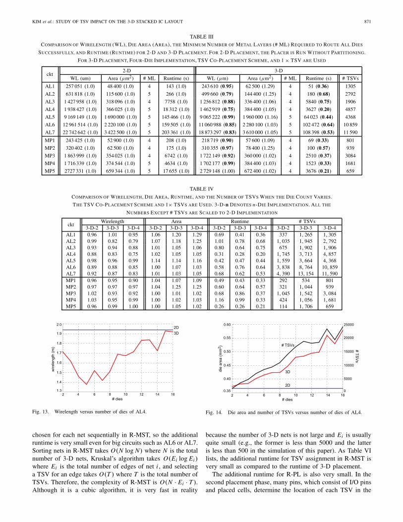
Table III shows wirelength, die area, and runtime of 2-D and3-D placement results. For 2-D placement, the 3-D placer isrun in a 2-D mode in which partitioning is not executed. For3-D placement, the TSV co-placement scheme is used withfour dies and 1×TSVs.
As to wirelength, wirelength of all the circuits except MP5is reduced. In the MP5 case, the wirelength of the four-die 3-Dimplementation is almost the same as that of its 2-D imple-mentation. Except MP5, the amount of wirelength reductionin nonmicroprocessor circuits (AL1 to AL7) is 1% to 25%,but the amount of wirelength reduction in microprocessorcircuits (MP1 to MP4) is 1% to 10%.
To figure out why nonmicroprocessor circuits have morewirelength reduction than microprocessor circuits, wirelengthdistributions of AL4 and MP5 are shown in Fig. 12. InFig. 12(a), long interconnections of AL4 in the 2-D designbecome shorter in the 3-D design. The longest wire in the 2-Ddesign of AL4 is about 900 μm long, whereas that in the 3-Ddesign is about 310 μm long. This effect is due to the smallerfootprint area and connections in the z-direction by TSVs.
The wirelength distribution of the 2-D design of MP5 isvery similar to that of the 3-D design of MP5 as shownin Fig. 12(b). The lengths of the longest wires in the2-D and the 3-D designs are also similar. Therefore, evenif multiple dies are stacked, the total wirelength does notchange. Table II also supports this analysis. MP5 (0.463 mm2)is larger than AL4 (0.257 mm2), but the longest wire of MP5 isshorter than that of AL4 (730 μm versus 900 μm). Actually,the die width of MP5 implemented in 3-D is 410 μm, so
the corner-to-corner Manhattan distance is 820 μm, whichis longer than the longest wire (730 μm). However, the diewidth of AL4 implemented in 3-D is 310 μm, so the corner-to-corner Manhattan distance is 620 μm, which is shorter thanthe longest wire (900 μm). Therefore, AL4 benefits from 3-Dimplementation, but MP5 does not.
This is also related to the min-cut partitioning resultshown in Table II. For example, the min-cut size of AL4 in2-way partitioning is 1502 out of 109 K nets while that ofMP5 is 54 out of 169 K nets. This means that MP5 is ahighly modularized circuit, so it does not benefit from 3-Dimplementation with respect to wirelength.
Regarding runtime, 3-D placement in general needs shorterruntime than 2-D placement.3 The reason is that an initial3-D placement of a circuit is likely to have fewer overlaps thanan initial 2-D placement of the circuit because each die in a3-D IC has fewer cells to be placed. Since the force-directedquadratic placement algorithm spends a significant portion ofits runtime in overlap removal, having fewer cells in a dieimproves runtime. In Table III, the 3-D global placement is1.3× to 5× faster than the 2-D global placement.
Since the design of an IC needs routing as well as place-ment, the runtime for routing is also compared. The 3-Dplacement generates Ndie placement results. Therefore, globaland detailed routing for each die is run concurrently. Then,the runtime for routing of a 3-D IC is obtained by choosingthe maximum runtime. In this simulation, the ratio betweenthe runtime for routing of 2-D ICs and the runtime for routingof 3-D ICs is between 2.73 and 5.11. The runtime for routingof 3-D ICs is much smaller than that for routing of 2-D ICsbecause the area of each die of a 3-D IC is smaller than thatof its 2-D counterpart.
B. Metal Layers and Silicon Area Comparison
Since each die of a 3-D design has fewer cells than a2-D design, the number of metal layers required for 3-Ddesigns could be less than that for 2-D designs. Therefore,the minimum number of metal layers required to route all diessuccessfully is found and compared. For a fair comparison, thesame area utilization is used for both 2-D and 3-D designs. The“# ML” columns in Table III list comparisons of the minimumnumber of metal layers in 2-D and 3-D designs. Except forAL5, AL6, and AL7, all circuits are routable with four metallayers in their 3-D designs, but the 2-D designs of AL2, AL4,AL5, AL6, AL7, MP4, and MP5 are not routable with fourmetal layers because of high routing congestion.
Table III also shows the area overhead of 3-D IC layouts.For small circuits, the area overhead is large (6% to 29%).However, the area overhead in large circuits is relativelysmall (2% to 16%). Since the area overhead is determinedby the number of TSVs, if few TSVs are used for a smalldesign, its area overhead could be negligible. Likewise, if toomany TSVs are used for a large design, the area overheadcould be significant.
3Partitioning used as a pre-process of 3-D placement for 3-D ICs needsa small fraction (0.05% to 2.5% in our simulation) of runtime for 3-Dplacement.

870 IEEE TRANSACTIONS ON VERY LARGE SCALE INTEGRATION (VLSI) SYSTEMS, VOL. 21, NO. 5, MAY 2013
TSV co-placement TSV site
Fig. 11. Cadence Virtuoso snapshot of the bottommost die of AL1 designed by TSV co-placement and TSV site schemes. Bright squares are TSVs.
wirelength (µm)(a)
# oc
curr
ence
s
2D3D
1 10 100 1000wirelength (µm)(b)
2D3D
# oc
curr
ence
s
10
104
103
102
1
10
104
103
102
11 10 100 1000
Fig. 12. Wirelength distribution of (a) nonmicroprocessor circuit (AL4)whose die width is 605 μm in a 2-D design and 310 μm in a 3-D design(4 dies) and (b) microprocessor circuit (MP5) whose die width is 812 μm ina 2-D design and 410 μm in a 3-D design (4 dies).
The area of 3-D designs is always larger than that of 2-Ddesigns in the simulation. However, the area of a 2-D designcould be larger than that of its 3-D design. As seen in Table III,some 2-D designs are not routable with four metal layers.Therefore, if there is a tight constraint on the available metallayers (e.g., four metal layers), the 2-D design not routableunder the constraint should be expanded. In this case, the areaof a 2-D design could be larger than that of its 3-D design.
C. On Wirelength and Die Area Versus Number of Dies
As the number of dies increases, the footprint area tendsto decrease,4 so the wirelength is expected to decrease while
4When the number of dies increases, if the TSV area is ignored, the footprintarea monotonically decreases. However, the number of TSVs has a great effecton the footprint area. If too many TSVs are used in a particular partitioningcase, the footprint area at that die count could increase.
the total die area is expected to increase. Therefore, howwirelength and die area vary when the die count increasesare observed in this section. In this simulation, the TSVco-placement scheme and 1 × TSVs are used.
Table IV lists wirelength, die area, runtime, and the numberof TSVs when the die count varies from two to four. As the diecount goes up, in general, the number of TSVs increases, butthe wirelength decreases for the nonmicroprocessor circuits.For further experiment on this, the number of dies (Ndie) isvaried from 2 to 16, and wirelength, die area, and the numberof TSVs are observed for AL4 in Fig. 13. The wirelength ofAL4 dramatically decreases as Ndie increases from two to five,then it generally goes up. If Ndie increases further, the TSVcount and the die area increase as shown in Fig. 14. In otherwords, increasing Ndie is helpful at first, but becomes harmfulat a larger number of dies because the TSV count increasesas Ndie goes up, which increases die area.
D. TSV Co-Placement Versus TSV Site
Table V lists the wirelength of five different placementschemes: the TSV co-placement (IR), the MST-based TSVsite placement (R-MST), the placement-based TSV siteplacement (R-PL), the neighborhood search-based TSV siteplacement (R-NS, [29]), and the network flow-based TSVsite placement (R-NF, [31]). The TSV co-placement (IR)designs always show shorter wirelength than the TSV siteplacement designs. The amount of wirelength reduction of IRas compared to R-MST, R-PL, R-NS, and R-NF is approxi-mately 4%, 8%, and 10% on average in two-die, three-die, andfour-die implementations, respectively. A reason that the TSVco-placement scheme produces shorter wirelength than theTSV site placement schemes is because the TSV co-placementscheme optimizes TSV locations and cell locations simultane-ously, while pre-placed TSVs in the TSV site schemes obstructoptimal gate placement.
Table VI lists the additional runtime required for TSVassignment in R-MST and R-PL. Since TSV assignment isan additional process after 3-D placement, runtime for 3-Dplacement is also reported in IR and R columns. TSVs are
KIM et al.: STUDY OF TSV IMPACT ON THE 3-D STACKED IC LAYOUT 871
TABLE III
COMPARISON OF WIRELENGTH (WL), DIE AREA (AREA), THE MINIMUM NUMBER OF METAL LAYERS (# ML) REQUIRED TO ROUTE ALL DIES
SUCCESSFULLY, AND RUNTIME (RUNTIME) FOR 2-D AND 3-D PLACEMENT. FOR 2-D PLACEMENT, THE PLACER IS RUN WITHOUT PARTITIONING.
FOR 3-D PLACEMENT, FOUR-DIE IMPLEMENTATION, TSV CO-PLACEMENT SCHEME, AND 1 × TSV ARE USED
ckt2-D 3-D
WL (um) Area (μm2) # ML Runtime (s) WL (μm) Area (μm2) # ML Runtime (s) # TSVs
AL1 257 051 (1.0) 48 400 (1.0) 4 143 (1.0) 243 610 (0.95) 62 500 (1.29) 4 51 (0.36) 1305
AL2 631 818 (1.0) 115 600 (1.0) 5 266 (1.0) 499 660 (0.79) 144 400 (1.25) 4 180 (0.68) 2792
AL3 1 427 958 (1.0) 318 096 (1.0) 4 7758 (1.0) 1 256 812 (0.88) 336 400 (1.06) 4 5840 (0.75) 1906
AL4 1 938 427 (1.0) 366 025 (1.0) 5 18 312 (1.0) 1 462 919 (0.75) 384 400 (1.05) 4 3627 (0.20) 4857
AL5 9 169 149 (1.0) 1 690 000 (1.0) 5 145 466 (1.0) 9 065 222 (0.99) 1 960 000 (1.16) 5 64 023 (0.44) 4368
AL6 12 961 514 (1.0) 2 220 100 (1.0) 5 159 505 (1.0) 11 060 988 (0.85) 2 280 100 (1.03) 5 102 472 (0.64) 10 859
AL7 22 742 642 (1.0) 3 422 500 (1.0) 5 203 361 (1.0) 18 873 297 (0.83) 3 610 000 (1.05) 5 108 398 (0.53) 11 590
MP1 243 425 (1.0) 52 900 (1.0) 4 208 (1.0) 218 719 (0.90) 57 600 (1.09) 4 69 (0.33) 801
MP2 320 402 (1.0) 62 500 (1.0) 4 175 (1.0) 310 355 (0.97) 78 400 (1.25) 4 100 (0.57) 939
MP3 1 863 999 (1.0) 354 025 (1.0) 4 6742 (1.0) 1 722 149 (0.92) 360 000 (1.02) 4 2510 (0.37) 3084
MP4 1 716 339 (1.0) 374 544 (1.0) 5 4634 (1.0) 1 702 177 (0.99) 384 400 (1.03) 4 1523 (0.33) 1681
MP5 2727 331 (1.0) 659 344 (1.0) 5 17 655 (1.0) 2 729 148 (1.00) 672 400 (1.02) 4 3676 (0.21) 659
TABLE IV
COMPARISON OF WIRELENGTH, DIE AREA, RUNTIME, AND THE NUMBER OF TSVS WHEN THE DIE COUNT VARIES.
THE TSV CO-PLACEMENT SCHEME AND 1× TSVS ARE USED. 3-D-n DENOTES n-DIE IMPLEMENTATION. ALL THE
NUMBERS EXCEPT # TSVS ARE SCALED TO 2-D IMPLEMENTATION
cktWirelength Area Runtime # TSVs
3-D-2 3-D-3 3-D-4 3-D-2 3-D-3 3-D-4 3-D-2 3-D-3 3-D-4 3-D-2 3-D-3 3-D-4AL1 0.96 1.01 0.95 1.06 1.20 1.29 0.69 0.41 0.36 337 1, 265 1, 305AL2 0.99 0.82 0.79 1.07 1.18 1.25 1.01 0.78 0.68 1, 035 1, 945 2, 792AL3 0.93 0.94 0.88 1.01 1.05 1.06 0.80 0.64 0.75 675 1, 902 1, 906AL4 0.88 0.83 0.75 1.02 1.05 1.05 0.31 0.28 0.20 1, 745 3, 713 4, 857AL5 0.98 0.96 0.99 1.14 1.14 1.16 0.42 0.47 0.44 1, 559 3, 664 4, 368AL6 0.89 0.88 0.85 1.00 1.07 1.03 0.58 0.76 0.64 3, 838 8, 764 10, 859AL7 0.92 0.87 0.83 1.01 1.03 1.05 0.68 0.62 0.53 4, 390 13, 154 11, 590MP1 0.96 0.95 0.90 1.04 1.07 1.09 0.49 0.43 0.33 292 534 801MP2 0.97 0.97 0.97 1.04 1.25 1.25 0.60 0.64 0.57 321 1, 044 939MP3 1.02 0.93 0.92 1.00 1.01 1.02 0.68 0.86 0.37 1, 045 1, 542 3, 084MP4 1.03 0.95 0.99 1.00 1.02 1.03 1.16 0.99 0.33 424 1, 056 1, 681MP5 0.96 0.99 1.00 1.00 1.05 1.02 0.26 0.26 0.21 114 1, 706 659
# dies42 6 8 10 12 1614
2D3D
wire
leng
th (m
)
2.0
1.9
1.8
1.7
1.6
1.5
1.4
1.3
Fig. 13. Wirelength versus number of dies of AL4.
chosen for each net sequentially in R-MST, so the additionalruntime is very small even for big circuits such as AL6 or AL7.Sorting nets in R-MST takes O(N log N) where N is the totalnumber of 3-D nets, Kruskal’s algorithm takes O(Ei log Ei )where Ei is the total number of edges of net i , and selectinga TSV for an edge takes O(T ) where T is the total number ofTSVs. Therefore, the complexity of R-MST is O(N · Ei · T ).Although it is a cubic algorithm, it is very fast in reality
# dies42 6 8 10 12 1614
0.40
0.45
0.60
die
area
(mm
2 )
0.55
0.50
0.352D
3D
# TSVs
5000
10000
25000
# TSV
s
20000
15000
0
Fig. 14. Die area and number of TSVs versus number of dies of AL4.
because the number of 3-D nets is not large and Ei is usuallyquite small (e.g., the former is less than 5000 and the latteris less than 500 in the simulation of this paper). As Table VIlists, the additional runtime for TSV assignment in R-MST isvery small as compared to the runtime of 3-D placement.
The additional runtime for R-PL is also very small. In thesecond placement phase, many pins, which consist of I/O pinsand placed cells, determine the location of each TSV in the

872 IEEE TRANSACTIONS ON VERY LARGE SCALE INTEGRATION (VLSI) SYSTEMS, VOL. 21, NO. 5, MAY 2013
TABLE V
WIRELENGTH COMPARISON FOR TSV PLACEMENT TYPES (SCALED TO THE 2-D PLACEMENT RESULT). IR DENOTES TSV CO-PLACEMENT, R-MST IS
MST-BASED TSV SITE PLACEMENT, R-PL IS PLACEMENT-BASED TSV SITE PLACEMENT, AND R-NS IS THE TSV SITE PLACEMENT SCHEME USING
THE NEIGHBORHOOD SEARCH-BASED TSV ASSIGNMENT PRESENTED IN [29]. 1× TSVS ARE USED. 3-D-n DENOTES n-DIE IMPLEMENTATION
ckt 2-D 3-D-2 3-D-3 3-D-4IR R-MST R-PL R-NS R-NF IR R-MST R-PL R-NS R-NF IR R-MST R-PL R-NS R-NF
AL1 257 051 μm (1.00) 0.96 1.02 1.04 1.05 1.00 1.01 1.08 1.11 1.10 1.07 0.95 1.05 1.05 1.07 1.04AL2 631 818 μm (1.00) 0.99 1.10 1.12 1.14 1.07 0.82 0.95 0.96 0.95 0.95 0.79 0.93 0.92 0.92 –AL3 1 427 958 μm (1.00) 0.93 1.00 1.00 0.99 0.98 0.94 0.98 1.03 1.02 0.96 0.88 0.95 0.96 0.96 0.94AL4 1 938 427 μm (1.00) 0.88 0.93 0.94 0.94 0.93 0.83 0.95 0.99 0.96 – 0.75 0.82 0.85 0.83 –AL5 9 169 149 μm (1.00) 0.98 1.01 1.02 1.03 1.00 0.96 1.05 1.05 1.04 – 0.99 1.03 1.03 1.03 –AL6 12 961 514 μm (1.00) 0.89 0.93 0.96 0.95 – 0.88 0.97 1.01 1.00 – 0.85 0.95 0.99 0.98 –AL7 22 742 642 μm (1.00) 0.92 0.96 0.97 0.97 – 0.87 0.96 0.99 0.98 – 0.83 0.88 0.91 0.92 –MP1 243 425 μm (1.00) 0.96 1.05 1.05 1.06 1.04 0.95 1.01 1.06 1.04 1.00 0.90 0.98 0.98 0.97 0.97MP2 320 402 μm (1.00) 0.97 1.00 1.00 1.00 1.00 0.97 1.02 1.05 1.02 1.02 0.97 1.02 1.03 1.03 1.03MP3 1 863 999 μm (1.00) 1.02 1.04 1.04 1.04 1.04 0.93 0.98 0.99 0.99 0.97 0.92 1.01 1.02 1.01 –MP4 1 716 339 μm (1.00) 1.03 1.07 1.08 1.08 1.07 0.95 1.00 1.01 1.01 0.99 0.99 1.06 1.06 1.06 1.04MP5 2 727 331 μm (1.00) 0.96 1.01 1.01 1.02 1.00 0.99 1.04 1.04 1.04 1.04 1.00 1.05 1.05 1.07 1.05
Geomean 1.00 0.96 1.01 1.02 1.02 0.92 1.00 1.02 1.01 0.90 0.97 0.99 0.98
TABLE VI
COMPARISON OF RUNTIME FOR TSV ASSIGNMENT FOR THE TWO TSV SITE PLACEMENT SCHEMES SHOWN IN TABLE V. IR AND R DENOTE
RUNTIMES OF TSV CO-PLACEMENT AND TSV SITE PLACEMENT, RESPECTIVELY. A(R-MST) AND A(R-PL) DENOTE ADDITIONAL RUNTIMES FOR
TSV ASSIGNMENT OF R-MST AND R-PL, RESPECTIVELY. THE UNIT IS SECOND (THE NUMBERS IN PARENTHESES DENOTE TOTAL ITERATION
COUNTS OF MATRIX COMPUTATION DURING PLACEMENT)
ckt3-D-2 3-D-3 3-D-4
Placement Assignment Placement Assignment Placement AssignmentIR R A(R-MST) A(R-PL) IR R A(R-MST) A(R-PL) IR R A(R-MST) A(R-PL)
AL1 98 77 0.14 0.18 (0) 58 72 0.28 0.71 (0) 51 70 0.25 0.77 (0)AL2 267 260 0.30 0.51 (0) 207 208 0.52 1.28 (0) 180 195 0.70 2.11 (0)AL3 6, 229 5, 691 0.69 0.81 (0) 4, 983 3, 577 1.05 1.33 (0) 5, 840 4, 950 0.99 0.70 (0)AL4 5, 622 5, 287 0.34 2.77 (0) 5, 078 4, 106 0.98 2.94 (0) 3, 627 3, 911 1.37 4.76 (0)AL5 61, 113 63 034 5.02 19.25 (0) 68 388 55 658 8.55 49.41 (1) 64 023 47 863 10.53 63.21 (2)AL6 92 865 137 784 23.81 8.59 (0) 121 686 125 777 36.32 9.33 (0) 102 472 101 031 40.32 13.51 (0)AL7 139 077 141 031 51.30 13.87 (0) 126 811 107 942 136.59 18.85 (0) 108 398 95 871 95.71 17.08 (0)MP1 102 119 0.97 0.89 (1) 90 109 0.95 0.46 (0) 69 75 0.97 0.61 (0)MP2 105 114 0.25 0.21 (0) 112 102 0.37 0.50 (0) 100 82 0.30 0.44 (0)MP3 4613 5932 0.84 1.32 (0) 5835 4943 0.49 1.92 (0) 2510 4925 1.37 2.35 (0)MP4 5354 5130 0.10 0.93 (0) 4569 4023 0.23 1.21 (0) 1523 2201 0.41 1.78 (0)MP5 4551 6312 0.15 1.04 (0) 4551 5298 0.57 1.87 (0) 3676 3563 0.22 2.00 (0)
initial placement, so little overlap exists between TSVs. Thus,the placement in R-PL needs only a few iterations of matrixcomputation. The numbers in parentheses in Table VI showthe number of iterations. Almost all of them are zero excepta few cases in which only one or two iterations are necessaryto remove all the overlaps among TSVs and cells.
On the other hand, the runtime for R-NS is almostnegligible and the runtime for R-NF is prohibitively high.Therefore, the runtime for R-NS and R-NF is not shownin Table VI.
E. Impact of TSV Size
Using large TSVs results in large die area overhead, therebydegrading total wirelength. It also causes more serious overlapamong TSVs and cells, thereby increasing runtime for 3-Dplacement. Therefore, the impact of TSV size on wirelength,die area, and runtime is investigated in this simulation.
Table VII lists the results for 1×, 2×, and 3× TSV size.Wirelength always increases as the TSV size increases, as doesthe die area. When the TSV becomes 2× larger, the wirelengthincreases by 9% on average and the die area increases by 27%on average. However, the wirelength becomes 28% longer and
TABLE VII
COMPARISON OF WIRELENGTH, DIE AREA, AND RUNTIME WHEN THE
TSV SIZE VARIES. THE TSV CO-PLACEMENT SCHEME IS USED WITH
FOUR DIES (SCALED TO THE 1 × TSV CASE)
ckt Wirelength Area Runtime1× 2× 3× 1× 2× 3× 1× 2× 3×
AL1 1.00 1.04 1.68 1.00 1.46 2.20 1.00 1.87 2.21AL2 1.00 1.14 1.37 1.00 1.68 2.74 1.00 1.63 1.95AL3 1.00 1.08 1.32 1.00 1.16 1.72 1.00 1.55 1.80AL4 1.00 1.18 1.36 1.00 1.31 2.05 1.00 1.32 1.30AL5 1.00 1.07 1.12 1.00 1.12 1.30 1.00 1.44 1.62AL6 1.00 1.11 1.14 1.00 1.35 1.58 1.00 1.34 1.77AL7 1.00 1.07 1.10 1.00 1.19 1.42 1.00 1.36 1.41MP1 1.00 1.20 1.75 1.00 1.38 2.01 1.00 1.38 2.11MP2 1.00 1.06 1.34 1.00 1.37 1.92 1.00 1.50 1.86MP3 1.00 1.07 1.21 1.00 1.20 1.70 1.00 2.11 3.59MP4 1.00 1.03 1.09 1.00 1.11 1.40 1.00 1.52 2.30MP5 1.00 1.01 1.05 1.00 1.08 1.36 1.00 1.03 1.14
Geomean 1.00 1.09 1.28 1.00 1.27 1.74 1.00 1.48 1.84
the die area becomes 74% larger on average when the TSVbecomes 3× larger. The runtime increase is also not negligible.Therefore, the use of larger TSVs causes serious wirelength,area, and runtime overhead.

KIM et al.: STUDY OF TSV IMPACT ON THE 3-D STACKED IC LAYOUT 873
TABLE VIII
WIRELENGTH COMPARISON (×105 μm) WITH [15] AND [17]
ckt [15] [17] This paper ckt [15] [17] This paper
AL1 2.84 2.59 2.44 MP1 3.01 2.39 2.19
AL2 5.83 5.52 5.00 MP2 3.88 3.87 3.10
AL3 14.01 13.51 12.57 MP3 20.02 17.87 17.22
AL4 19.12 22.91 14.63 MP4 26.83 18.27 17.02
MP5 39.46 29.80 27.29
Avg. 1.00 1.01 0.84 1.00 0.84 0.74
VII. CONCLUSION
In this paper, the impact of TSVs on the 3-D stackedIC layout has been investigated. First, design issues newlyintroduced in 3-D ICs were discussed, and then two 3-D ICdesign flows were proposed. In the TSV co-placement scheme,gates and TSVs were placed simultaneously, whereas in theTSV site scheme, TSVs were uniformly placed and then gateswere placed. The simulation results showed that 3-D designshave shorter wirelength, require fewer metal layers for routing,and shorter runtime for placement. However, die area increasesbecause of TSV insertion. In conclusion, 3-D IC designmethodologies and algorithms should take TSV placement androuting into account, which our 3-D IC design methodologiesand algorithms perform effectively and efficiently.
APPENDIX
The 3-D global placer presented in [15] has been improvedfor this paper. Table VIII compares wirelength of [15], [17],and this paper.
REFERENCES
[1] J. W. Joyner, P. Zarkesh-Ha, J. A. Davis, and J. D. Meindl, “A three-dimensional stochastic wire-length distribution for variable separation ofstrata,” in Proc. IEEE Int. Interconnect Technol. Conf., Jun. 2000, pp.126–128.
[2] D. H. Kim, S. Mukhopadhyay, and S. K. Lim, “Through-silicon-viaaware interconnect prediction and optimization for 3D stacked ICs,” inProc. ACM/IEEE Int. Workshop Syst. Level Interconnect Predict., Jul.2009, pp. 85–92.
[3] T. Thorolfsson, K. Gonsalves, and P. D. Franzon, “Design automationfor a 3DIC FFT processor for synthetic aperture radar: A case study,”in Proc. ACM Design Autom. Conf., Jul. 2009, pp. 51–56.
[4] D. H. Kim and S. K. Lim, “Through-silicon-via-aware delay andpower prediction model for buffered interconnects in 3D ICs,” in Proc.ACM/IEEE Int. Workshop Syst. Level Interconnect Predict., Jun. 2010,pp. 25–32.
[5] X. Dong and Y. Xie, “System-level cost analysis and design explorationfor three-dimensional integrated circuits (3D ICs),” in Proc. Asia SouthPacific Design Autom. Conf., Jan. 2009, pp. 234–241.
[6] K. Bernstein, P. Andry, J. Cann, P. Emma, D. Greenberg, W. Haensch,M. Ignatowski, S. Koester, J. Magerlein, and R. Puri, “Interconnectsin the third dimension: Design challenges for 3D ICs,” in Proc. ACMDesign Autom. Conf., Jun. 2007, pp. 562–567.
[7] E. Beyne, P. D. Moor, W. Ruythooren, R. Labie, A. Jourdain, H. Tilmans,D. S. Tezcan, P. Soussan, B. Swinnen, and R. Cartuyvels, “Through-silicon via and die stacking technologies for microsystems-integration,”in Proc. IEEE IEDM, Dec. 2008, pp. 1–4.
[8] M. Koyanagi, T. Fukushima, and T. Tanaka, “High-density throughsilicon vias for 3-D LSIs,” Proc. IEEE, vol. 97, no. 1, pp. 49–59, Jan.2009.
[9] H. Chaabouni, M. Rousseau, P. Leduc, A. Farcy, R. El Farhane, A.Thuaire, G. Haury, A. Valentian, G. Billiot, M. Assous, F. De Crecy,J. Cluzel, A. Toffoli, D. Bouchu, L. Cadix, T. Lacrevaz, P. Ancey, N.Sillon, and B. Flechet, “Investigation on TSV impact on 65 nm CMOSdevices and circuits,” in Proc. IEEE IEDM, Dec. 2010, pp. 35–38.
[10] H. Y. Li, E. Liao, X. F. Pang, H. Yu, X. X. Yu, and J. Y. Sun, “Fastelectroplating TSV process development for the via-last approach,” inProc. IEEE Electron. Comp. Technol. Conf., Jun. 2010, pp. 777–780.
[11] J. Cong, G. Luo, J. Wei, and Y. Zhang, “Thermal-aware 3D IC placementvia transformation,” in Proc. Asia South Pacific Design Autom. Conf.,Jan. 2007, pp. 780–785.
[12] B. Goplen and S. Sapatnekar, “Placement of 3D ICs with thermal andinterlayer via considerations,” in Proc. ACM Design Autom. Conf., Jun.2007, pp. 626–631.
[13] B. Goplen and S. Sapatnekar, “Efficient thermal placement of standardcells in 3D ICs using a force directed approach,” in Proc. IEEE Int.Conf. Comput.-Aided Design, Nov. 2003, pp. 86–89.
[14] J. Cong and G. Luo, “A multilevel analytical placement for 3D ICs,” inProc. Asia South Pacific Design Autom. Conf., Jan. 2009, pp. 361–366.
[15] D. H. Kim, K. Athikulwongse, and S. K. Lim, “A study of through-silicon-via impact on the 3D stacked IC layout,” in Proc. IEEE Int.Conf. Comput.-Aided Design, Nov. 2009, pp. 674–680.
[16] M. Pathak, Y.-J. Lee, T. Moon, and S. K. Lim, “Through-silicon-viamanagement during 3D physical design: When to add and how many?”in Proc. IEEE Int. Conf. Comput.-Aided Design, Nov. 2010, pp. 387–394.
[17] M.-K. Hsu, Y.-W. Chang, and V. Balabanov, “TSV-aware analyticalplacement for 3D IC designs,” in Proc. ACM Design Autom. Conf., Jun.2011, pp. 664–669.
[18] G. Karypis and V. Kumar. hMETIS, a Hypergraph Partitioning Pack-age Version 1.5.3 [Online]. Available: http://glaros.dtc.umn.edu/gkhome/metis/hmetis/download
[19] IWLS 2005 Benchmarks. (2005) [Online]. Available: http://www.iwls.org/iwls2005
[20] FreePDK45. NCSU, Raleigh, NC [Online]. Available: http://www.eda.ncsu.edu/wiki/FreePDK
[21] Nangate 45 nm Open Cell Library. Nangate, Sunnyvale, CA [Online].Available: http://www.nangate.com
[22] A.-C. Hsieh, T. Hwang, M.-T. Chang, M.-H. Tsai, C.-M. Tseng, andH.-C. Li, “TSV redundancy: Architecture and design issues in 3D IC,”in Proc. Design, Autom. Test Eur., Mar. 2010, pp. 166–171.
[23] M. Jung, J. Mitra, D. Z. Pan, and S. K. Lim, “TSV stress-aware full-chip mechanical reliability analysis and optimization for 3D IC,” in Proc.ACM Design Autom. Conf., Jun. 2011, pp. 188–193.
[24] D. H. Kim, R. O. Topaloglu, and S. K. Lim, “TSV density-driven globalplacement for 3D stacked ICs,” in Proc. Int. SoC Design Conf., Nov.2011, pp. 135–138.
[25] FaStack. Tezzaron, Naperville, IL [Online]. Available: http://www.tezzaron.com
[26] J. Cong and S. K. Lim, “Edge separability based circuit clustering withapplication to multi-level circuit partitioning,” IEEE Trans. Comput.-Aided Design Integr. Circuits Syst., vol. 23, no. 3, pp. 346–357, Mar.2004.
[27] Soc Encounter. Cadence Design Systems, San Jose, CA [Online].Available: http://www.cadence.com
[28] P. Spindler, U. Schlichtmann, and F. M. Johannes, “Kraftwerk2–afast force-directed quadratic placement approach using an accuratenet model,” IEEE Trans. Comput.-Aided Design Integr. Circuits Syst.,vol. 27, no. 8, pp. 1398–1411, Aug. 2008.
[29] H. Yan, Z. Li, Q. Zhou, and X. Hong, “Via assignment algorithm forhierarchical 3-D placement,” in Proc. IEEE Int. Conf. Commun., CircuitsSyst., May 2005, pp. 1225–1229.
[30] H. W. Kuhn, “The Hungarian method for the assignment problem,”Naval Res. Logist., vol. 2, pp. 83–97, Mar. 1955.
[31] M.-C. Tsai, T.-C. Wang, and T. Hwang, “Through-silicon via planningin 3-D floorplanning,” IEEE Trans. Very Large Scale Integr. (VLSI) Syst.,vol. 19, no. 8, pp. 1448–1457, Aug. 2011.
Dae Hyun Kim (S’08) received the B.S. degree inelectrical engineering from Seoul National Univer-sity, Seoul, Korea, in 2002, and the M.S. degreein electrical and computer engineering from theGeorgia Institute of Technology, Atlanta, in 2007,where he is currently pursuing the Ph.D. degree withthe School of Electrical and Computer Engineering.
His current research interests include physicaldesign algorithms particularly for 3-D integratedcircuits, design methodology, placement, routing,and design for manufacturability.

874 IEEE TRANSACTIONS ON VERY LARGE SCALE INTEGRATION (VLSI) SYSTEMS, VOL. 21, NO. 5, MAY 2013
Krit Athikulwongse (S’04) received the B.Eng.,M.Eng., and M.S. degrees from the Departmentof Electrical Engineering, Chulalongkorn University,Bangkok, Thailand, in 1995, 1997, and 2005, respec-tively. He is currently pursuing the Ph.D. degree withthe School of Electrical and Computer Engineering,Georgia Institute of Technology (Georgia Tech),Atlanta.
He joined the Computer Aided Design Laboratory,Georgia Tech, in 2008. His current research interestsinclude physical design for 3-D integrated circuits.
Sung Kyu Lim (S’94–M’00–SM’05) received theB.S., M.S., and Ph.D. degrees from the ComputerScience Department, University of California, LosAngeles, in 1994, 1997, and 2000, respectively.
He joined the School of Electrical and Com-puter Engineering, Georgia Institute of Technology,Atlanta, in 2001, where he is currently an Asso-ciate Professor. He has been leading the Cross-Center Theme on 3-D Integration for the FocusCenter Research Program, Semiconductor ResearchCorporation, Durham, NC, since 2009. His current
research interests include architectures, circuits, physical design for 3-Dintegrated circuits, and 3-D system-in-packages. He is the author of PracticalProblems in VLSI Physical Design Automation (Springer, 2008).
Dr. Lim was a recipient of the Design Automation Conference GraduateScholarship in 2003, the National Science Foundation Faculty Early CareerDevelopment CAREER Award in 2006, and the ACM SIGDA DistinguishedService Award in 2008. He was on the Advisory Board of the ACM SpecialInterest Group on Design Automation (SIGDA) from 2003 to 2008. Hewas an Associate Editor of the IEEE TRANSACTIONS ON VERY LARGE
SCALE INTEGRATION (VLSI) SYSTEMS from 2007 to 2009. His paperswere nominated for the Best Paper Award at the International Symposium onPhysical Design in 2006, the International Conference on Computer-AidedDesign in 2009, the Custom Integrated Circuits Conference in 2010, andthe Design Automation Conference in 2011 and 2012. He was a memberof the Design International Technology Working Group for the Renewal ofthe International Technology Roadmap for Semiconductors in 2009.