8/16-bit Atmel XMEGA A1U...
216
Atmel-8385I-AVR-ATxmega64A1U-128A1U-Datasheet–09/2014 Features z High-performance, low-power Atmel ® AVR ® XMEGA ® 8/16-bit Microcontroller z Nonvolatile program and data memories z 64K - 128KBytes of in-system self-programmable flash z 4K - 8KBytes boot section z 2KBytes EEPROM z 4K - 8KBytes internal SRAM z External bus interface for up to 16Mbytes SRAM z External bus interface for up to 128Mbit SDRAM z Peripheral features z Four-channel DMA controller z Eight-channel event system z Eight 16-bit timer/counters z Four timer/counters with 4 output compare or input capture channels z Four timer/counters with 2 output compare or input capture channels z High resolution extension on all timer/counters z Advanced waveform extension (AWeX) on two timer/counters z One USB device interface z USB 2.0 full speed (12Mbps) and low speed (1.5Mbps) device compliant z 32 Endpoints with full configuration flexibility z Eight USARTs with IrDA support for one USART z Four two-wire interfaces with dual address match (I 2 C and SMBus compatible) z Four serial peripheral interfaces (SPIs) z AES and DES crypto engine z CRC-16 (CRC-CCITT) and CRC-32 (IEEE ® 802.3) generator z 16-bit real time counter (RTC) with separate oscillator z Two sixteen channel, 12-bit, 2msps Analog to Digital Converters z Two Two-channel, 12-bit, 1msps Digital to Analog Converters z Four Analog Comparators (ACs) with window compare function, and current sources z External interrupts on all general purpose I/O pins z Programmable watchdog timer with separate on-chip ultra low power oscillator z QTouch ® library support z Capacitive touch buttons, sliders and wheels z Special microcontroller features z Power-on reset and programmable brown-out detection z Internal and external clock options with PLL and prescaler z Programmable multilevel interrupt controller z Five sleep modes z Programming and debug interfaces z JTAG (IEEE 1149.1 compliant) interface, including boundary scan z PDI (Program and Debug Interface) z I/O and packages z 78 Programmable I/O pins z 100 lead TQFP z 100 ball BGA z 100 ball VFBGA z Operating voltage z 1.6 – 3.6V z Operating frequency z 0 – 12MHz from 1.6V z 0 – 32MHz from 2.7V 8/16-bit Atmel XMEGA A1U Microcontroller ATxmega128A1U / ATxmega64A1U
Transcript of 8/16-bit Atmel XMEGA A1U...
Atmel-8385I-AVR-ATxmega64A1U-128A1U-Datasheet–09/2014
Features
z High-performance, low-power Atmel® AVR® XMEGA® 8/16-bit Microcontrollerz Nonvolatile program and data memories
z 64K - 128KBytes of in-system self-programmable flashz 4K - 8KBytes boot sectionz 2KBytes EEPROMz 4K - 8KBytes internal SRAM
z External bus interface for up to 16Mbytes SRAMz External bus interface for up to 128Mbit SDRAM
z Peripheral featuresz Four-channel DMA controllerz Eight-channel event systemz Eight 16-bit timer/counters
z Four timer/counters with 4 output compare or input capture channelsz Four timer/counters with 2 output compare or input capture channelsz High resolution extension on all timer/countersz Advanced waveform extension (AWeX) on two timer/counters
z One USB device interfacez USB 2.0 full speed (12Mbps) and low speed (1.5Mbps) device compliantz 32 Endpoints with full configuration flexibility
z Eight USARTs with IrDA support for one USARTz Four two-wire interfaces with dual address match (I2C and SMBus compatible)z Four serial peripheral interfaces (SPIs)z AES and DES crypto enginez CRC-16 (CRC-CCITT) and CRC-32 (IEEE® 802.3) generatorz 16-bit real time counter (RTC) with separate oscillatorz Two sixteen channel, 12-bit, 2msps Analog to Digital Convertersz Two Two-channel, 12-bit, 1msps Digital to Analog Convertersz Four Analog Comparators (ACs) with window compare function, and current sourcesz External interrupts on all general purpose I/O pinsz Programmable watchdog timer with separate on-chip ultra low power oscillatorz QTouch® library support
z Capacitive touch buttons, sliders and wheelsz Special microcontroller features
z Power-on reset and programmable brown-out detectionz Internal and external clock options with PLL and prescalerz Programmable multilevel interrupt controllerz Five sleep modesz Programming and debug interfaces
z JTAG (IEEE 1149.1 compliant) interface, including boundary scanz PDI (Program and Debug Interface)
z I/O and packagesz 78 Programmable I/O pinsz 100 lead TQFPz 100 ball BGAz 100 ball VFBGA
z Operating voltagez 1.6 – 3.6V
z Operating frequencyz 0 – 12MHz from 1.6Vz 0 – 32MHz from 2.7V
8/16-bit Atmel XMEGA A1U Microcontroller
ATxmega128A1U / ATxmega64A1U
2XMEGA A1U [DATASHEET]Atmel-8385I-AVR-ATxmega64A1U-128A1U-Datasheet–09/2014
1. Ordering Information
Notes: 1. This device can also be supplied in wafer form. Please contact your local Atmel sales office for detailed ordering information.2. Pb-free packaging, complies to the European Directive for Restriction of Hazardous Substances (RoHS directive). Also Halide free and fully Green.3. For packaging information, see “Packaging information” on page 71.4. Tape and Reel.
Typical Applications
Ordering code Flash (bytes)EEPROM (bytes)
SRAM (bytes) Speed (MHz)
Power supply
Package (1)(2)(3) Temp.
ATxmega128A1U-AU 128K + 8K 2K 8K
32 1.6 - 3.6V
100A
-40°C - 85°C
ATxmega128A1U-AUR(4) 128K + 8K 2K 8K
ATxmega64A1U-AU 64K + 4K 2K 4K
ATxmega64A1U-AUR(4) 64K + 4K 2K 4K
ATxmega128A1U-CU 128K + 8K 2K 8K
100C1ATxmega128A1U-CUR(4) 128K + 8K 2K 8K
ATxmega64A1U-CU 64K + 4K 2K 4K
ATxmega64A1U-CUR(4) 64K + 4K 2K 4K
ATxmega128A1U-C7U 128K + 8K 2K 8K
100C2ATxmega128A1U-C7UR(4) 128K + 8K 2K 8K
ATxmega64A1U-C7U 64K + 4K 2K 4K
ATxmega64A1U-C7UR(4) 64K + 4K 2K 4K
ATxmega128A1U-AN 128K + 8K 2K 8K
100A -40°C - 105°CATxmega128A1U-ANR(4) 128K + 8K 2K 8K
ATxmega64A1U-AN 64K + 4K 2K 4K
ATxmega64A1U-ANR(4) 64K + 4K 2K 4K
Package Type
100A 100-lead, 14 x 14 x 1.0mm, 0.5mm lead pitch, thin profile plastic quad flat package (TQFP)
100C1 100-ball, 9 x 9 x 1.2mm body, ball pitch 0.80mm, chip ball grid array (CBGA)
100C2 100-ball, 7 x 7 x 1.0mm body, ball pitch 0.65mm, very thin fine-pitch ball grid array (VFBGA)
Industrial control Climate control Low power battery applications
Factory automation RF and ZigBee® Power tools
Building control USB connectivity HVAC
Board control Sensor control Utility metering
White goods Optical Medical applications
3XMEGA A1U [DATASHEET]Atmel-8385I-AVR-ATxmega64A1U-128A1U-Datasheet–09/2014
2. Pinout/Block Diagram
Figure 2-1. Block diagram and pinout.
For details on pinout and pin functions refer to “Pinout and Pin Functions” on page 56.
1
2
3
4
5
6
7
8
9
10
11
12
13
14
15
16
17
18
19
20
21
22
23
24
25
75
74
73
72
71
70
69
68
67
66
65
64
63
62
61
60
59
58
57
56
55
54
53
52
51
26 27 28 29 30 31 32 33 34 35 36 37 38 39 40 41 42 43 44 45 46 47 48 49 50
AV
CC
GN
D
GND
AVCC
GND
VCC
GN
D
VCC
GN
D
VCC
VCC
GND
VCC
GND
VCC
GND
GND
VCC
PA0
PA1
PA2
PA3
PB0
PB1
PB3
PB2
PB7
PB5
PB4
PB6
PA4
PA5
PA7
PA6
PDI/R
ESET
PDI
PR0
PR1
GN
D
VCC
PQ0
PQ1
PQ2
PQ3
PJ7
PJ6
PJ5
PJ4
PJ3
PJ2
PJ1
PJ0
PK7
PK6
PK5
PK4
PK3
PK2
PK1
PK0
PH7
PH6
PH5
PH3
PH2
PH1
PH0
PH4
PC0
PC1
PC2
PC3
PC4
PC5
PC6
PC7
PD0
PD1
PD2
PD3
PD4
PD5
PD6
PD7
PE0
PE1
PE2
PE3
PE4
PE5
PE6
PE7
PF0
PF1
PF2
PF3
PF4
PF5
PF7
PF6
100 99 98 97 96 95 94 93 92 91 90 89 88 87 86 85 84 83 82 81 80 79 78 77 76
Power Supervision
Port
A
EVENT ROUTING NETWORK
DMA Controller
BUS matrix
SRAMFLASH
ADC
AC0:1
OCD
Port EPort D
Prog/DebugInterface
EEPROM
Port C
TC0:
1
Event System Controller
Watchdog Timer
WatchdogOscillator
OSC/CLK Control
Real TimeCounter
Interrupt Controller
DATA BUS
DATA BUS
Port RUS
ART0
:1
TWI
SPI
TC0:
1
USAR
T0:1
SPI
TC0:
1
USAR
T0:1
TWI
SPI
Port
B
ADC
DAC
AC0:1
AREF
JTAG
AREF
SleepController
ResetController
InternalReference
IRCO
M
Crypto / CRC
USB
DACTW
I
Port F
TC0:
1
USAR
T0:1
TWI
SPI
Exte
rnal
Bus
Inte
rface Po
rt K
Port
JPo
rt H
Port Q
CPU
XOSC TOSC
InternalOscillators
Digital functionAnalog function / Oscillators
Programming, debug, testExternal clock / Crystal pinsGeneral Purpose I/O
Ground
EBI
Power
4XMEGA A1U [DATASHEET]Atmel-8385I-AVR-ATxmega64A1U-128A1U-Datasheet–09/2014
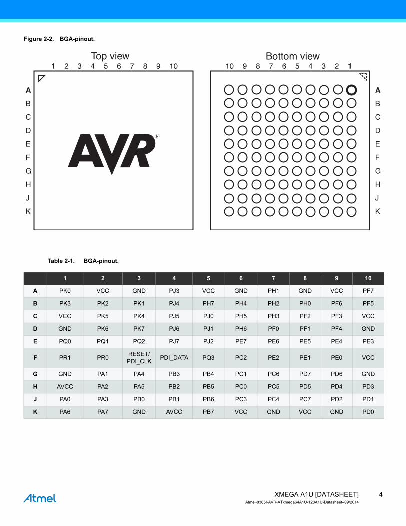
Figure 2-2. BGA-pinout.
Table 2-1. BGA-pinout.
AB
C
D
E
F
G
H
J
K
1 2 3 4 5 6 7 8 9 10
AB
C
D
E
F
G
H
J
K
10 9 8 7 6 5 4 3 2 1Top view Bottom view
1 2 3 4 5 6 7 8 9 10
A PK0 VCC GND PJ3 VCC GND PH1 GND VCC PF7
B PK3 PK2 PK1 PJ4 PH7 PH4 PH2 PH0 PF6 PF5
C VCC PK5 PK4 PJ5 PJ0 PH5 PH3 PF2 PF3 VCC
D GND PK6 PK7 PJ6 PJ1 PH6 PF0 PF1 PF4 GND
E PQ0 PQ1 PQ2 PJ7 PJ2 PE7 PE6 PE5 PE4 PE3
F PR1 PR0 RESET/PDI_CLK PDI_DATA PQ3 PC2 PE2 PE1 PE0 VCC
G GND PA1 PA4 PB3 PB4 PC1 PC6 PD7 PD6 GND
H AVCC PA2 PA5 PB2 PB5 PC0 PC5 PD5 PD4 PD3
J PA0 PA3 PB0 PB1 PB6 PC3 PC4 PC7 PD2 PD1
K PA6 PA7 GND AVCC PB7 VCC GND VCC GND PD0

5XMEGA A1U [DATASHEET]Atmel-8385I-AVR-ATxmega64A1U-128A1U-Datasheet–09/2014
3. OverviewThe Atmel AVR XMEGA is a family of low power, high performance, and peripheral rich 8/16-bit microcontrollers based on the AVR enhanced RISC architecture. By executing instructions in a single clock cycle, the AVR XMEGA devices achieve CPU throughput approaching one million instructions per second (MIPS) per megahertz, allowing the system designer to optimize power consumption versus processing speed.
The Atmel AVR CPU combines a rich instruction set with 32 general purpose working registers. All 32 registers are directly connected to the arithmetic logic unit (ALU), allowing two independent registers to be accessed in a single instruction, executed in one clock cycle. The resulting architecture is more code efficient while achieving throughputs many times faster than conventional single-accumulator or CISC based microcontrollers.
The AVR XMEGA A1U devices provide the following features: in-system programmable flash with read-while-write capabilities; internal EEPROM and SRAM; four-channel DMA controller, eight-channel event system and programmable multilevel interrupt controller, 78 general purpose I/O lines, 16-bit real-time counter (RTC); eight flexible, 16-bit timer/counters with compare and PWM channels, eight USARTs; four two-wire serial interfaces (TWIs); one full speed USB 2.0 interface; four serial peripheral interfaces (SPIs); AES and DES cryptographic engine; CRC-16 (CRC-CCITT) and CRC-32 (IEEE 802.3) generator; two 16-channel, 12-bit ADCs with programmable gain; two 2-channel, 12-bit DACs; four Analog Comparators (ACs) with window mode; programmable watchdog timer with separate internal oscillator; accurate internal oscillators with PLL and prescaler; and programmable brown-out detection.
The program and debug interface (PDI), a fast, two-pin interface for programming and debugging, is available. The devices also have an IEEE std. 1149.1 compliant JTAG interface, and this can also be used for boundary scan, on-chip debug and programming.
The XMEGA A1U devices have five software selectable power saving modes. The idle mode stops the CPU while allowing the SRAM, DMA controller, event system, interrupt controller, and all peripherals to continue functioning. The power-down mode saves the SRAM and register contents, but stops the oscillators, disabling all other functions until the next TWI, USB resume, or pin-change interrupt, or reset. In power-save mode, the asynchronous real-time counter continues to run, allowing the application to maintain a timer base while the rest of the device is sleeping. In standby mode, the external crystal oscillator keeps running while the rest of the device is sleeping. This allows very fast startup from the external crystal, combined with low power consumption. In extended standby mode, both the main oscillator and the asynchronous timer continue to run. To further reduce power consumption, the peripheral clock to each individual peripheral can optionally be stopped in active mode and idle sleep mode.
Atmel offers a free QTouch library for embedding capacitive touch buttons, sliders and wheels functionality into AVR microcontrollers.
The device are manufactured using Atmel high-density, nonvolatile memory technology. The program flash memory can be reprogrammed in-system through the PDI or JTAG interfaces. A boot loader running in the device can use any interface to download the application program to the flash memory. The boot loader software in the boot flash section will continue to run while the application flash section is updated, providing true read-while-write operation. By combining an 8/16-bit RISC CPU with in-system, self-programmable flash, the AVR XMEGA is a powerful microcontroller family that provides a highly flexible and cost effective solution for many embedded applications.
All Atmel AVR XMEGA devices are supported with a full suite of program and system development tools, including C compilers, macro assemblers, program debugger/simulators, programmers, and evaluation kits.
6XMEGA A1U [DATASHEET]Atmel-8385I-AVR-ATxmega64A1U-128A1U-Datasheet–09/2014
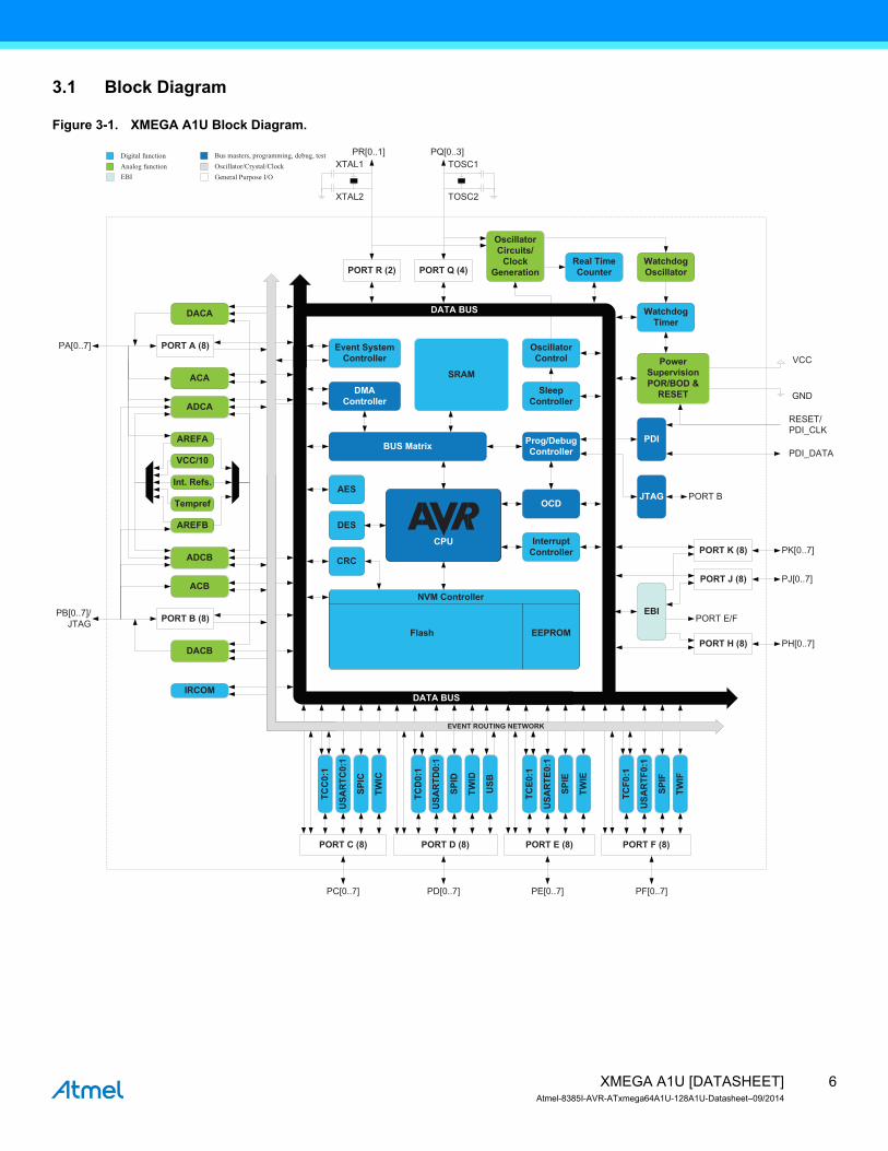
3.1 Block Diagram
Figure 3-1. XMEGA A1U Block Diagram.
Power SupervisionPOR/BOD &
RESET
PORT A (8)
PORT B (8)
EVENT ROUTING NETWORK
DMAController
SRAM
EBI
ADCA
DACA
ACA
DACB
ADCB
ACB
OCD
Int. Refs.
PORT K (8)
PORT J (8)
PORT H (8)
PDI
PH[0..7]
PJ[0..7]
PK[0..7]
PA[0..7]
PB[0..7]/JTAG
Watchdog Timer
WatchdogOscillator
Interrupt Controller
DATA BUS
Prog/DebugController
VCC
GND
Oscillator Circuits/
Clock Generation
Oscillator Control
Real TimeCounter
Event System Controller
JTAG
AREFA
AREFB
PDI_DATA
RESET/PDI_CLK
PORT B
Sleep Controller
DES
CRC
PORT C (8)
PC[0..7]
TCC0
:1
USAR
TC0:
1
TWIC
SPIC
PD[0..7] PE[0..7] PF[0..7]
PORT D (8)
TCD0
:1
USAR
TD0:
1
TWID
SPID
TCF0
:1
USAR
TF0:
1
TWIF
SPIF
TCE0
:1
USAR
TE0:
1
TWIE
SPIE
PORT E (8) PORT F (8)
Tempref
VCC/10
AESUS
B
PORT R (2)
XTAL1
XTAL2
PR[0..1]TOSC1
TOSC2
PQ[0..3]
PORT Q (4)
DATA BUS
NVM Controller
MORPEEhsalF
IRCOM
BUS Matrix
CPU
PORT E/F
Digital functionAnalog function
Bus masters, programming, debug, testOscillator/Crystal/ClockGeneral Purpose I/OEBI
7XMEGA A1U [DATASHEET]Atmel-8385I-AVR-ATxmega64A1U-128A1U-Datasheet–09/2014
4. ResourcesA comprehensive set of development tools, application notes and datasheets are available for download on http://www.atmel.com/avr.
4.1 Recommended readingz Atmel AVR XMEGA AU manualz XMEGA application notes
This device data sheet only contains part specific information with a short description of each peripheral and module. The XMEGA AU manual describes the modules and peripherals in depth. The XMEGA application notes contain example code and show applied use of the modules and peripherals.
All documentations are available from www.atmel.com/avr.
5. Capacitive touch sensingThe Atmel QTouch library provides a simple to use solution to realize touch sensitive interfaces on most Atmel AVR microcontrollers. The patented charge-transfer signal acquisition offers robust sensing and includes fully debounced reporting of touch keys and includes Adjacent Key Suppression® (AKS®) technology for unambiguous detection of key events. The QTouch library includes support for the QTouch and QMatrix acquisition methods.
Touch sensing can be added to any application by linking the appropriate Atmel QTouch library for the AVR microcontroller. This is done by using a simple set of APIs to define the touch channels and sensors, and then calling the touch sensing API’s to retrieve the channel information and determine the touch sensor states.
The QTouch library is FREE and downloadable from the Atmel website at the following location: www.atmel.com/qtouchlibrary. For implementation details and other information, refer to the QTouch library user guide - also available for download from the Atmel website.
8XMEGA A1U [DATASHEET]Atmel-8385I-AVR-ATxmega64A1U-128A1U-Datasheet–09/2014
6. AVR CPU
6.1 Featuresz 8/16-bit, high-performance Atmel AVR RISC CPU
z 142 instructionsz Hardware multiplier
z 32x8-bit registers directly connected to the ALUz Stack in RAMz Stack pointer accessible in I/O memory spacez Direct addressing of up to 16MB of program memory and 16MB of data memoryz True 16/24-bit access to 16/24-bit I/O registersz Efficient support for 8-, 16-, and 32-bit arithmeticz Configuration change protection of system-critical features
6.2 OverviewAll Atmel AVR XMEGA devices use the 8/16-bit AVR CPU. The main function of the CPU is to execute the code and perform all calculations. The CPU is able to access memories, perform calculations, control peripherals, and execute the program in the flash memory. Interrupt handling is described in a separate section, refer to “Interrupts and Programmable Multilevel Interrupt Controller” on page 27.
6.3 Architectural OverviewIn order to maximize performance and parallelism, the AVR CPU uses a Harvard architecture with separate memories and buses for program and data. Instructions in the program memory are executed with single-level pipelining. While one instruction is being executed, the next instruction is pre-fetched from the program memory. This enables instructions to be executed on every clock cycle. For details of all AVR instructions, refer to http://www.atmel.com/avr.
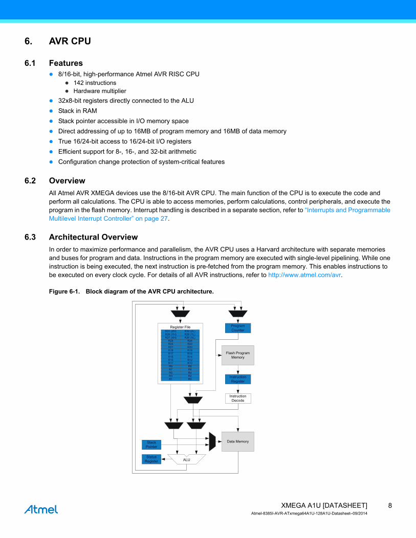
Figure 6-1. Block diagram of the AVR CPU architecture.

9XMEGA A1U [DATASHEET]Atmel-8385I-AVR-ATxmega64A1U-128A1U-Datasheet–09/2014
The arithmetic logic unit (ALU) supports arithmetic and logic operations between registers or between a constant and a register. Single-register operations can also be executed in the ALU. After an arithmetic operation, the status register is updated to reflect information about the result of the operation.
The ALU is directly connected to the fast-access register file. The 32 x 8-bit general purpose working registers all have single clock cycle access time allowing single-cycle arithmetic logic unit (ALU) operation between registers or between a register and an immediate. Six of the 32 registers can be used as three 16-bit address pointers for program and data space addressing, enabling efficient address calculations.
The memory spaces are linear. The data memory space and the program memory space are two different memory spaces.
The data memory space is divided into I/O registers, SRAM, and external RAM. In addition, the EEPROM can be memory mapped in the data memory.
All I/O status and control registers reside in the lowest 4KB addresses of the data memory. This is referred to as the I/O memory space. The lowest 64 addresses can be accessed directly, or as the data space locations from 0x00 to 0x3F. The rest is the extended I/O memory space, ranging from 0x0040 to 0x0FFF. I/O registers here must be accessed as data space locations using load (LD/LDS/LDD) and store (ST/STS/STD) instructions.
The SRAM holds data. Code execution from SRAM is not supported. It can easily be accessed through the five different addressing modes supported in the AVR architecture. The first SRAM address is 0x2000.
Data addresses 0x1000 to 0x1FFF are reserved for memory mapping of EEPROM.
The program memory is divided in two sections, the application program section and the boot program section. Both sections have dedicated lock bits for write and read/write protection. The SPM instruction that is used for self-programming of the application flash memory must reside in the boot program section. The application section contains an application table section with separate lock bits for write and read/write protection. The application table section can be used for safe storing of nonvolatile data in the program memory.
6.4 ALU - Arithmetic Logic UnitThe arithmetic logic unit (ALU) supports arithmetic and logic operations between registers or between a constant and a register. Single-register operations can also be executed. The ALU operates in direct connection with all 32 general purpose registers. In a single clock cycle, arithmetic operations between general purpose registers or between a register and an immediate are executed and the result is stored in the register file. After an arithmetic or logic operation, the status register is updated to reflect information about the result of the operation.
ALU operations are divided into three main categories – arithmetic, logical, and bit functions. Both 8- and 16-bit arithmetic is supported, and the instruction set allows for efficient implementation of 32-bit aritmetic. The hardware multiplier supports signed and unsigned multiplication and fractional format.
6.4.1 Hardware Multiplier
The multiplier is capable of multiplying two 8-bit numbers into a 16-bit result. The hardware multiplier supports different variations of signed and unsigned integer and fractional numbers:z Multiplication of unsigned integersz Multiplication of signed integersz Multiplication of a signed integer with an unsigned integerz Multiplication of unsigned fractional numbersz Multiplication of signed fractional numbersz Multiplication of a signed fractional number with an unsigned one
A multiplication takes two CPU clock cycles.
10XMEGA A1U [DATASHEET]Atmel-8385I-AVR-ATxmega64A1U-128A1U-Datasheet–09/2014
6.5 Program FlowAfter reset, the CPU starts to execute instructions from the lowest address in the flash programmemory ‘0.’ The program counter (PC) addresses the next instruction to be fetched.
Program flow is provided by conditional and unconditional jump and call instructions capable of addressing the whole address space directly. Most AVR instructions use a 16-bit word format, while a limited number use a 32-bit format.
During interrupts and subroutine calls, the return address PC is stored on the stack. The stack is allocated in the general data SRAM, and consequently the stack size is only limited by the total SRAM size and the usage of the SRAM. After reset, the stack pointer (SP) points to the highest address in the internal SRAM. The SP is read/write accessible in the I/O memory space, enabling easy implementation of multiple stacks or stack areas. The data SRAM can easily be accessed through the five different addressing modes supported in the AVR CPU.
6.6 Status RegisterThe status register (SREG) contains information about the result of the most recently executed arithmetic or logic instruction. This information can be used for altering program flow in order to perform conditional operations. Note that the status register is updated after all ALU operations, as specified in the instruction set reference. This will in many cases remove the need for using the dedicated compare instructions, resulting in faster and more compact code.
The status register is not automatically stored when entering an interrupt routine nor restored when returning from an interrupt. This must be handled by software.
The status register is accessible in the I/O memory space.
6.7 Stack and Stack PointerThe stack is used for storing return addresses after interrupts and subroutine calls. It can also be used for storing temporary data. The stack pointer (SP) register always points to the top of the stack. It is implemented as two 8-bit registers that are accessible in the I/O memory space. Data are pushed and popped from the stack using the PUSH and POP instructions. The stack grows from a higher memory location to a lower memory location. This implies that pushing data onto the stack decreases the SP, and popping data off the stack increases the SP. The SP is automatically loaded after reset, and the initial value is the highest address of the internal SRAM. If the SP is changed, it must be set to point above address 0x2000, and it must be defined before any subroutine calls are executed or before interrupts are enabled.
During interrupts or subroutine calls, the return address is automatically pushed on the stack. The return address can be two or three bytes, depending on program memory size of the device. For devices with 128KB or less of program memory, the return address is two bytes, and hence the stack pointer is decremented/incremented by two. For devices with more than 128KB of program memory, the return address is three bytes, and hence the SP is decremented/incremented by three. The return address is popped off the stack when returning from interrupts using the RETI instruction, and from subroutine calls using the RET instruction.
The SP is decremented by one when data are pushed on the stack with the PUSH instruction, and incremented by one when data is popped off the stack using the POP instruction.
To prevent corruption when updating the stack pointer from software, a write to SPL will automatically disable interrupts for up to four instructions or until the next I/O memory write.
After reset the stack pointer is initialized to the highest address of the SRAM. See Figure 7-2 on page 14.
6.8 Register FileThe register file consists of 32 x 8-bit general purpose working registers with single clock cycle access time. The register file supports the following input/output schemes:z One 8-bit output operand and one 8-bit result inputz Two 8-bit output operands and one 8-bit result inputz Two 8-bit output operands and one 16-bit result inputz One 16-bit output operand and one 16-bit result input
11XMEGA A1U [DATASHEET]Atmel-8385I-AVR-ATxmega64A1U-128A1U-Datasheet–09/2014
Six of the 32 registers can be used as three 16-bit address register pointers for data space addressing, enabling efficient address calculations. One of these address pointers can also be used as an address pointer for lookup tables in flash program memory.
7. Memories
7.1 Featuresz Flash program memory
z One linear address spacez In-system programmablez Self-programming and boot loader supportz Application section for application codez Application table section for application code or data storagez Boot section for application code or boot loader codez Separate read/write protection lock bits for all sectionsz Built in fast CRC check of a selectable flash program memory section
z Data memoryz One linear address spacez Single-cycle access from CPUz SRAMz EEPROM
z Byte and page accessiblez Optional memory mapping for direct load and store
z I/O memoryz Configuration and status registers for all peripherals and modulesz 16 bit-accessible general purpose register for global variables or flags
z External memory supportz SRAMz SDRAMz Memory mapped external hardware
z Bus arbitrationz Deterministic priority handling between CPU, DMA controller, and other bus masters
z Separate buses for SRAM, EEPROM, I/O memory and external memoryz Simultaneous bus access for CPU and DMA controller
z Production signature row memory for factory programmed dataz ID for each microcontroller device typez Serial number for each devicez Calibration bytes for factory calibrated peripherals
z User signature rowz One flash page in sizez Can be read and written from softwarez Content is kept after chip erase
7.2 OverviewThe Atmel AVR architecture has two main memory spaces, the program memory and the data memory. Executable code can reside only in the program memory, while data can be stored in the program memory and the data memory. The data memory includes the internal SRAM, and EEPROM for nonvolatile data storage. All memory spaces are linear and require no memory bank switching. Nonvolatile memory (NVM) spaces can be locked for further write and read/write operations. This prevents unrestricted access to the application software.
A separate memory section contains the fuse bytes. These are used for configuring important system functions, and can only be written by an external programmer.
12XMEGA A1U [DATASHEET]Atmel-8385I-AVR-ATxmega64A1U-128A1U-Datasheet–09/2014
The available memory size configurations are shown in “Ordering Information” on page 2. In addition each device has a flash memory signature rows for calibration data, device identification, serial number etc.
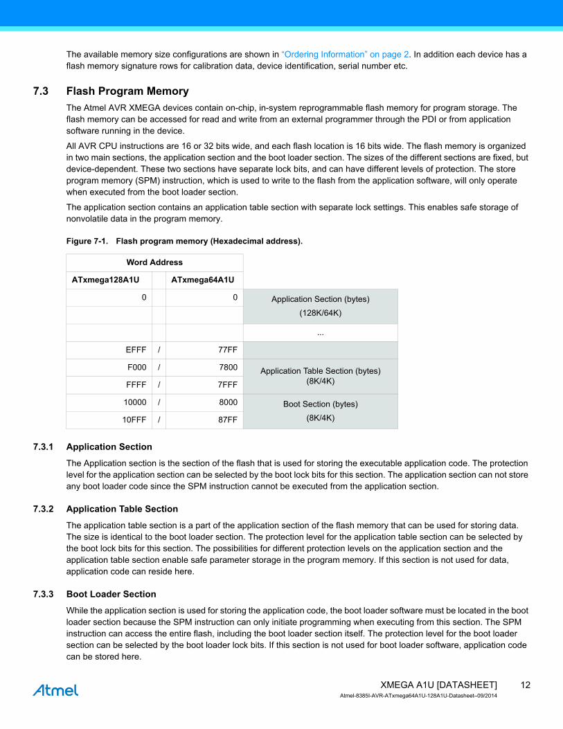
7.3 Flash Program MemoryThe Atmel AVR XMEGA devices contain on-chip, in-system reprogrammable flash memory for program storage. The flash memory can be accessed for read and write from an external programmer through the PDI or from application software running in the device.
All AVR CPU instructions are 16 or 32 bits wide, and each flash location is 16 bits wide. The flash memory is organized in two main sections, the application section and the boot loader section. The sizes of the different sections are fixed, but device-dependent. These two sections have separate lock bits, and can have different levels of protection. The store program memory (SPM) instruction, which is used to write to the flash from the application software, will only operate when executed from the boot loader section.
The application section contains an application table section with separate lock settings. This enables safe storage of nonvolatile data in the program memory.
Figure 7-1. Flash program memory (Hexadecimal address).
7.3.1 Application Section
The Application section is the section of the flash that is used for storing the executable application code. The protection level for the application section can be selected by the boot lock bits for this section. The application section can not store any boot loader code since the SPM instruction cannot be executed from the application section.
7.3.2 Application Table Section
The application table section is a part of the application section of the flash memory that can be used for storing data. The size is identical to the boot loader section. The protection level for the application table section can be selected by the boot lock bits for this section. The possibilities for different protection levels on the application section and the application table section enable safe parameter storage in the program memory. If this section is not used for data, application code can reside here.
7.3.3 Boot Loader Section
While the application section is used for storing the application code, the boot loader software must be located in the boot loader section because the SPM instruction can only initiate programming when executing from this section. The SPM instruction can access the entire flash, including the boot loader section itself. The protection level for the boot loader section can be selected by the boot loader lock bits. If this section is not used for boot loader software, application code can be stored here.
Word Address
ATxmega128A1U ATxmega64A1U
0 0 Application Section (bytes)
(128K/64K)
...
EFFF / 77FF
F000 / 7800 Application Table Section (bytes) (8K/4K)FFFF / 7FFF
10000 / 8000 Boot Section (bytes)
(8K/4K)10FFF / 87FF
13XMEGA A1U [DATASHEET]Atmel-8385I-AVR-ATxmega64A1U-128A1U-Datasheet–09/2014
7.3.4 Production Signature Row
The production signature row is a separate memory section for factory programmed data. It contains calibration data for functions such as oscillators and analog modules. Some of the calibration values will be automatically loaded to the corresponding module or peripheral unit during reset. Other values must be loaded from the signature row and written to the corresponding peripheral registers from software. For details on calibration conditions, refer to “Electrical Characteristics” on page 74.
The production signature row also contains an ID that identifies each microcontroller device type and a serial number for each manufactured device. The serial number consists of the production lot number, wafer number, and wafer coordinates for the device. The device ID for the available devices is shown in Table 7-1.
The production signature row cannot be written or erased, but it can be read from application software and external programmers.
Table 7-1. Device ID bytes.
7.3.5 User Signature Row
The user signature row is a separate memory section that is fully accessible (read and write) from application software and external programmers. It is one flash page in size, and is meant for static user parameter storage, such as calibration data, custom serial number, identification numbers, random number seeds, etc. This section is not erased by chip erase commands that erase the flash, and requires a dedicated erase command. This ensures parameter storage during multiple program/erase operations and on-chip debug sessions.
7.4 Fuses and Lock bitsThe fuses are used to configure important system functions, and can only be written from an external programmer. The application software can read the fuses. The fuses are used to configure reset sources such as brownout detector and watchdog, startup configuration, JTAG enable, and JTAG user ID.
The lock bits are used to set protection levels for the different flash sections (that is, if read and/or write access should be blocked). Lock bits can be written by external programmers and application software, but only to stricter protection levels. Chip erase is the only way to erase the lock bits. To ensure that flash contents are protected even during chip erase, the lock bits are erased after the rest of the flash memory has been erased.
An unprogrammed fuse or lock bit will have the value one, while a programmed fuse or lock bit will have the value zero.
Both fuses and lock bits are reprogrammable like the flash program memory.
7.5 Data MemoryThe data memory contains the I/O memory, internal SRAM, optionally memory mapped EEPROM, and external memory if available. The data memory is organized as one continuous memory section, see Figure 7-2 on page 14. To simplify development, I/O Memory, EEPROM and SRAM will always have the same start addresses for all Atmel AVR XMEGA devices. The address space for External Memory will always start at the end of Internal SRAM and end at address 0xFFFFFF.
Device Device ID bytes
Byte 2 Byte 1 Byte 0
ATxmega64A1U 4E 96 1E
ATxmega128A1U 4C 97 1E
14XMEGA A1U [DATASHEET]Atmel-8385I-AVR-ATxmega64A1U-128A1U-Datasheet–09/2014
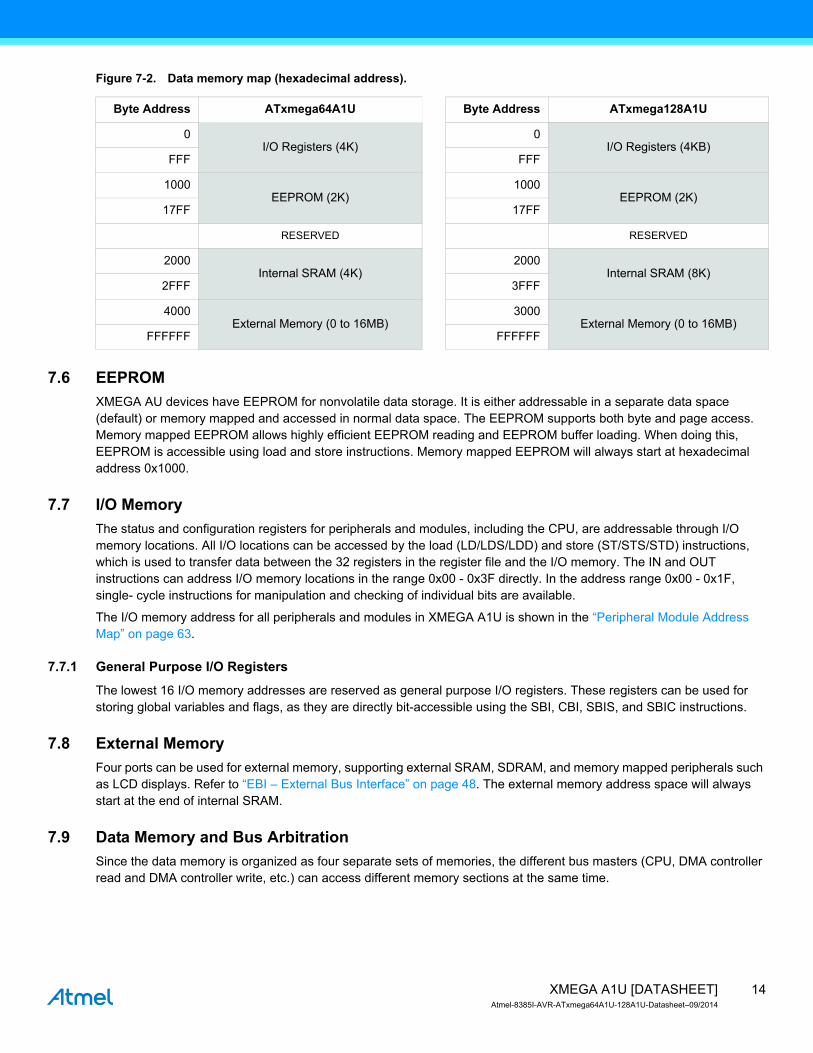
Figure 7-2. Data memory map (hexadecimal address).
7.6 EEPROMXMEGA AU devices have EEPROM for nonvolatile data storage. It is either addressable in a separate data space (default) or memory mapped and accessed in normal data space. The EEPROM supports both byte and page access. Memory mapped EEPROM allows highly efficient EEPROM reading and EEPROM buffer loading. When doing this, EEPROM is accessible using load and store instructions. Memory mapped EEPROM will always start at hexadecimal address 0x1000.
7.7 I/O MemoryThe status and configuration registers for peripherals and modules, including the CPU, are addressable through I/O memory locations. All I/O locations can be accessed by the load (LD/LDS/LDD) and store (ST/STS/STD) instructions, which is used to transfer data between the 32 registers in the register file and the I/O memory. The IN and OUT instructions can address I/O memory locations in the range 0x00 - 0x3F directly. In the address range 0x00 - 0x1F, single- cycle instructions for manipulation and checking of individual bits are available.
The I/O memory address for all peripherals and modules in XMEGA A1U is shown in the “Peripheral Module Address Map” on page 63.
7.7.1 General Purpose I/O Registers
The lowest 16 I/O memory addresses are reserved as general purpose I/O registers. These registers can be used for storing global variables and flags, as they are directly bit-accessible using the SBI, CBI, SBIS, and SBIC instructions.
7.8 External MemoryFour ports can be used for external memory, supporting external SRAM, SDRAM, and memory mapped peripherals such as LCD displays. Refer to “EBI – External Bus Interface” on page 48. The external memory address space will always start at the end of internal SRAM.
7.9 Data Memory and Bus ArbitrationSince the data memory is organized as four separate sets of memories, the different bus masters (CPU, DMA controller read and DMA controller write, etc.) can access different memory sections at the same time.
Byte Address ATxmega64A1U Byte Address ATxmega128A1U
0I/O Registers (4K)
0I/O Registers (4KB)
FFF FFF
1000EEPROM (2K)
1000EEPROM (2K)
17FF 17FF
RESERVED RESERVED
2000Internal SRAM (4K)
2000Internal SRAM (8K)
2FFF 3FFF
4000External Memory (0 to 16MB)
3000External Memory (0 to 16MB)
FFFFFF FFFFFF
15XMEGA A1U [DATASHEET]Atmel-8385I-AVR-ATxmega64A1U-128A1U-Datasheet–09/2014
7.10 Memory TimingRead and write access to the I/O memory takes one CPU clock cycle. A write to SRAM takes one cycle, and a read from SRAM takes two cycles. For burst read (DMA), new data are available every cycle. EEPROM page load (write) takes one cycle, and three cycles are required for read. For burst read, new data are available every second cycle. External memory has multi-cycle read and write. The number of cycles depends on the type of memory and configuration of the external bus interface. Refer to the instruction summary for more details on instructions and instruction timing.
7.11 Device ID and RevisionEach device has a three-byte device ID. This ID identifies Atmel as the manufacturer of the device and the device type. A separate register contains the revision number of the device.
7.12 I/O Memory ProtectionSome features in the device are regarded as critical for safety in some applications. Due to this, it is possible to lock the I/O register related to the clock system, the event system, and the advanced waveform extensions. As long as the lock is enabled, all related I/O registers are locked and they can not be written from the application software. The lock registers themselves are protected by the configuration change protection mechanism.
7.13 JTAG DisableIt is possible to disable the JTAG interface from the application software. This will prevent all external JTAG access to the device until the next device reset or until JTAG is enabled again from the application software. As long as JTAG is disabled, the I/O pins required for JTAG can be used as normal I/O pins.
7.14 Flash and EEPROM Page SizeThe flash program memory and EEPROM data memory are organized in pages. The pages are word accessible for the flash and byte accessible for the EEPROM.
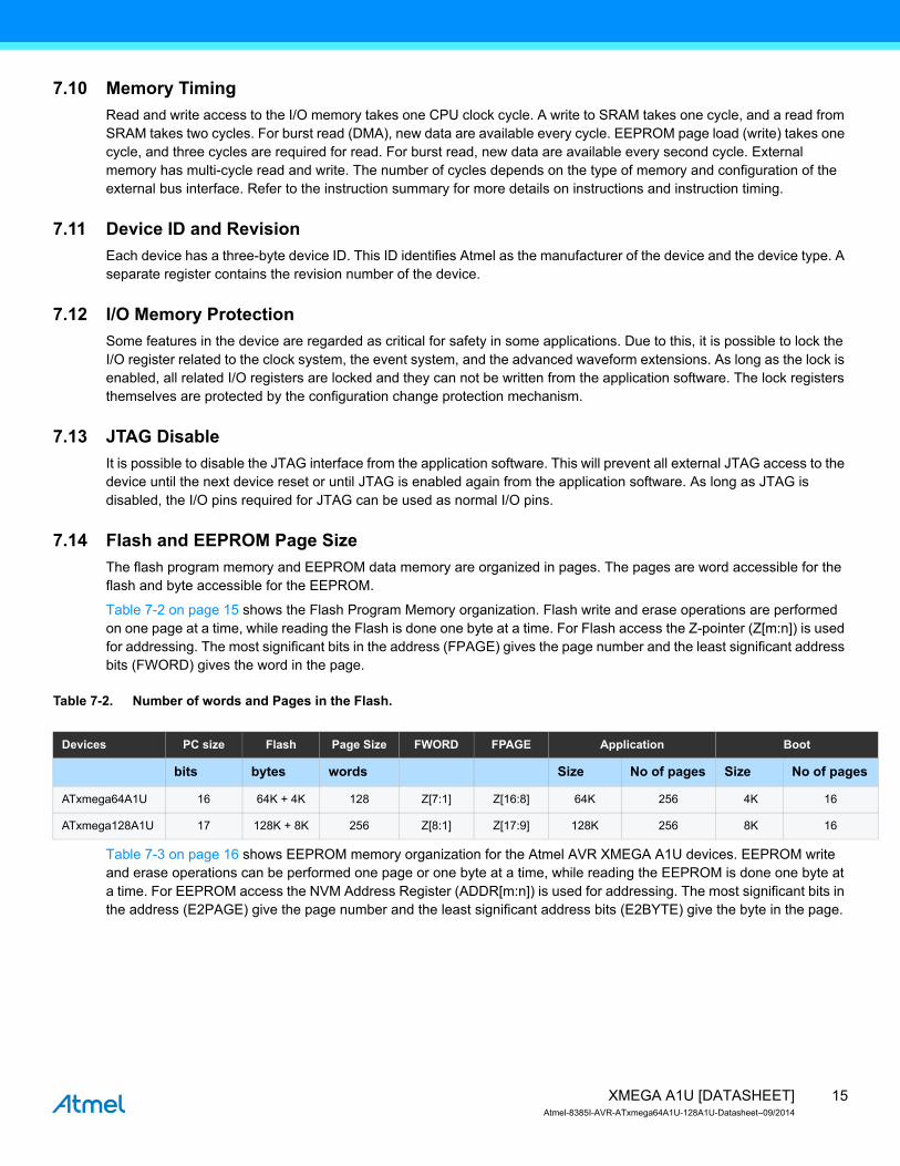
Table 7-2 on page 15 shows the Flash Program Memory organization. Flash write and erase operations are performed on one page at a time, while reading the Flash is done one byte at a time. For Flash access the Z-pointer (Z[m:n]) is used for addressing. The most significant bits in the address (FPAGE) gives the page number and the least significant address bits (FWORD) gives the word in the page.
Table 7-2. Number of words and Pages in the Flash.
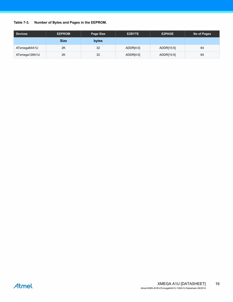
Table 7-3 on page 16 shows EEPROM memory organization for the Atmel AVR XMEGA A1U devices. EEPROM write and erase operations can be performed one page or one byte at a time, while reading the EEPROM is done one byte at a time. For EEPROM access the NVM Address Register (ADDR[m:n]) is used for addressing. The most significant bits in the address (E2PAGE) give the page number and the least significant address bits (E2BYTE) give the byte in the page.
Devices PC size Flash Page Size FWORD FPAGE Application Boot
bits bytes words Size No of pages Size No of pages
ATxmega64A1U 16 64K + 4K 128 Z[7:1] Z[16:8] 64K 256 4K 16
ATxmega128A1U 17 128K + 8K 256 Z[8:1] Z[17:9] 128K 256 8K 16
16XMEGA A1U [DATASHEET]Atmel-8385I-AVR-ATxmega64A1U-128A1U-Datasheet–09/2014
Table 7-3. Number of Bytes and Pages in the EEPROM.
Devices EEPROM Page Size E2BYTE E2PAGE No of Pages
Size bytes
ATxmega64A1U 2K 32 ADDR[4:0] ADDR[10:5] 64
ATxmega128A1U 2K 32 ADDR[4:0] ADDR[10:5] 64
17XMEGA A1U [DATASHEET]Atmel-8385I-AVR-ATxmega64A1U-128A1U-Datasheet–09/2014
8. DMAC – Direct Memory Access Controller
8.1 Featuresz Allows high speed data transfers with minimal CPU intervention
z from data memory to data memoryz from data memory to peripheralz from peripheral to data memoryz from peripheral to peripheral
z Four DMA channels with separatez transfer triggersz interrupt vectorsz addressing modes
z Programmable channel priorityz From 1 byte to 16MB of data in a single transaction
z Up to 64KB block transfers with repeatz 1, 2, 4, or 8 byte burst transfers
z Multiple addressing modesz Staticz Incrementalz Decremental
z Optional reload of source and destination addresses at the end of eachz Burstz Blockz Transaction
z Optional interrupt on end of transactionz Optional connection to CRC generator for CRC on DMA data
8.2 OverviewThe four-channel direct memory access (DMA) controller can transfer data between memories and peripherals, and thus offload these tasks from the CPU. It enables high data transfer rates with minimum CPU intervention, and frees up CPU time. The four DMA channels enable up to four independent and parallel transfers.
The DMA controller can move data between SRAM and peripherals, between SRAM locations and directly between peripheral registers. With access to all peripherals, the DMA controller can handle automatic transfer of data to/from communication modules. The DMA controller can also read from memory mapped EEPROM.
Data transfers are done in continuous bursts of 1, 2, 4, or 8 bytes. They build block transfers of configurable size from 1 byte to 64KB. A repeat counter can be used to repeat each block transfer for single transactions up to 16MB. Source and destination addressing can be static, incremental or decremental. Automatic reload of source and/or destination addresses can be done after each burst or block transfer, or when a transaction is complete. Application software, peripherals, and events can trigger DMA transfers.
The four DMA channels have individual configuration and control settings. This include source, destination, transfer triggers, and transaction sizes. They have individual interrupt settings. Interrupt requests can be generated when a transaction is complete or when the DMA controller detects an error on a DMA channel.
To allow for continuous transfers, two channels can be interlinked so that the second takes over the transfer when the first is finished, and vice versa.
18XMEGA A1U [DATASHEET]Atmel-8385I-AVR-ATxmega64A1U-128A1U-Datasheet–09/2014
9. Event System
9.1 Featuresz System for direct peripheral-to-peripheral communication and signalingz Peripherals can directly send, receive, and react to peripheral events
z CPU and DMA controller independent operationz 100% predictable signal timing z Short and guaranteed response time
z Eight event channels for up to eight different and parallel signal routing configurationsz Events can be sent and/or used by most peripherals, clock system, and softwarez Additional functions include
z Quadrature decodersz Digital filtering of I/O pin state
z Works in active mode and idle sleep mode
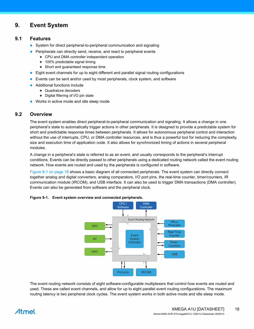
9.2 OverviewThe event system enables direct peripheral-to-peripheral communication and signaling. It allows a change in one peripheral’s state to automatically trigger actions in other peripherals. It is designed to provide a predictable system for short and predictable response times between peripherals. It allows for autonomous peripheral control and interaction without the use of interrupts, CPU, or DMA controller resources, and is thus a powerful tool for reducing the complexity, size and execution time of application code. It also allows for synchronized timing of actions in several peripheral modules.
A change in a peripheral’s state is referred to as an event, and usually corresponds to the peripheral’s interrupt conditions. Events can be directly passed to other peripherals using a dedicated routing network called the event routing network. How events are routed and used by the peripherals is configured in software.
Figure 9-1 on page 18 shows a basic diagram of all connected peripherals. The event system can directly connect together analog and digital converters, analog comparators, I/O port pins, the real-time counter, timer/counters, IR communication module (IRCOM), and USB interface. It can also be used to trigger DMA transactions (DMA controller). Events can also be generated from software and the peripheral clock.
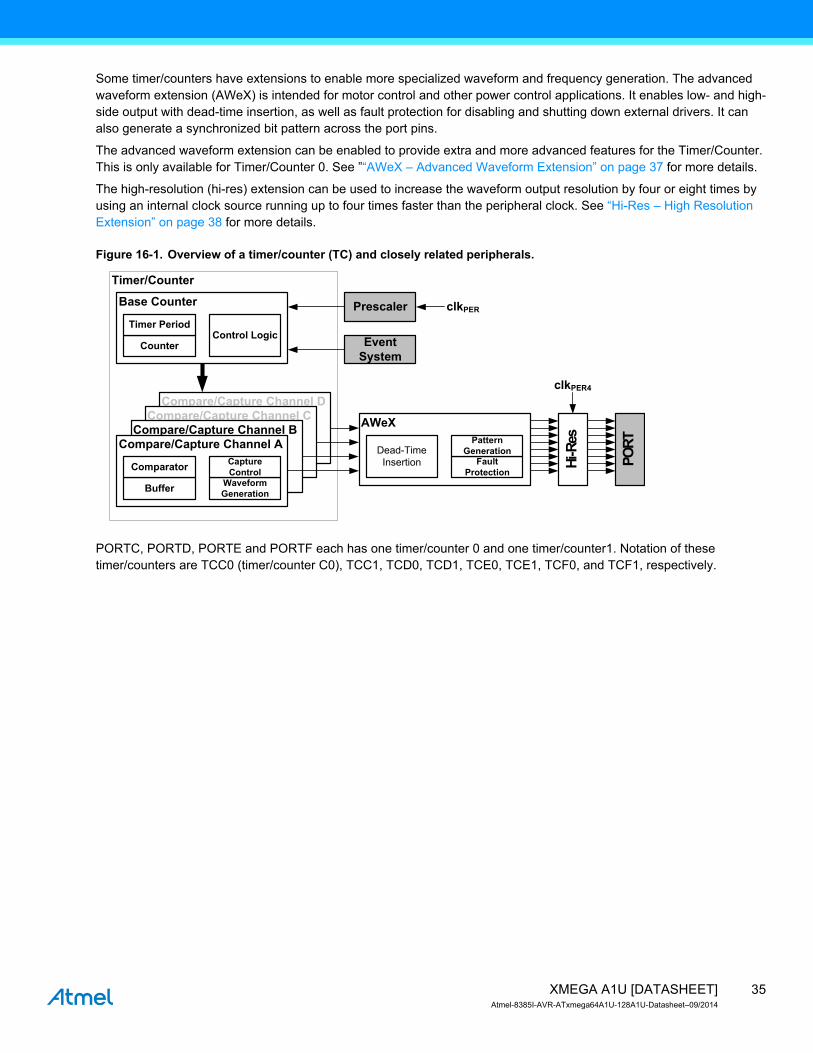
Figure 9-1. Event system overview and connected peripherals.
The event routing network consists of eight software-configurable multiplexers that control how events are routed and used. These are called event channels, and allow for up to eight parallel event routing configurations. The maximum routing latency is two peripheral clock cycles. The event system works in both active mode and idle sleep mode.
DAC
Timer / Counters
USB
ADC
Real Time Counter
Port pins
CPU / Software
DMAController
IRCOM
Event Routing Network
Event System
Controller
clkPERPrescaler
AC
19XMEGA A1U [DATASHEET]Atmel-8385I-AVR-ATxmega64A1U-128A1U-Datasheet–09/2014
10. System Clock and Clock options
10.1 Featuresz Fast start-up timez Safe run-time clock switchingz Internal oscillators:
z 32MHz run-time calibrated and tunable oscillatorz 2MHz run-time calibrated oscillator z 32.768kHz calibrated oscillatorz 32kHz ultra low power (ULP) oscillator with 1kHz output
z External clock optionsz 0.4MHz - 16MHz crystal oscillatorz 32.768kHz crystal oscillatorz External clock
z PLL with 20MHz - 128MHz output frequencyz Internal and external clock options and 1x to 31x multiplicationz Lock detector
z Clock prescalers with 1x to 2048x divisionz Fast peripheral clocks running at two and four times the CPU clockz Automatic run-time calibration of internal oscillatorsz External oscillator and PLL lock failure detection with optional non-maskable interrupt
10.2 OverviewAtmel AVR XMEGA devices have a flexible clock system supporting a large number of clock sources. It incorporates both accurate internal oscillators and external crystal oscillator and resonator support. A high-frequency phase locked loop (PLL) and clock prescalers can be used to generate a wide range of clock frequencies. A calibration feature (DFLL) is available, and can be used for automatic run-time calibration of the internal oscillators to remove frequency drift over voltage and temperature. An oscillator failure monitor can be enabled to issue a non-maskable interrupt and switch to the internal oscillator if the external oscillator or PLL fails.
When a reset occurs, all clock sources except the 32kHz ultra low power oscillator are disabled. After reset, the device will always start up running from the 2MHz internal oscillator. During normal operation, the system clock source and prescalers can be changed from software at any time.
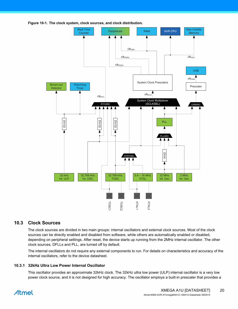
Figure 10-1 on page 20 presents the principal clock system in the XMEGA A1U family devices. Not all of the clocks need to be active at a given time. The clocks for the CPU and peripherals can be stopped using sleep modes and power reduction registers as described in “Power Management and Sleep Modes” on page 22.
20XMEGA A1U [DATASHEET]Atmel-8385I-AVR-ATxmega64A1U-128A1U-Datasheet–09/2014
Figure 10-1. The clock system, clock sources, and clock distribution.
10.3 Clock SourcesThe clock sources are divided in two main groups: internal oscillators and external clock sources. Most of the clock sources can be directly enabled and disabled from software, while others are automatically enabled or disabled, depending on peripheral settings. After reset, the device starts up running from the 2MHz internal oscillator. The other clock sources, DFLLs and PLL, are turned off by default.
The internal oscillators do not require any external components to run. For details on characteristics and accuracy of the internal oscillators, refer to the device datasheet.
10.3.1 32kHz Ultra Low Power Internal Oscillator
This oscillator provides an approximate 32kHz clock. The 32kHz ultra low power (ULP) internal oscillator is a very low power clock source, and it is not designed for high accuracy. The oscillator employs a built-in prescaler that provides a
Real TimeCounter Peripherals RAM AVR CPU Non-Volatile
Memory
WatchdogTimer
Brown-outDetector
System Clock Prescalers
USB
Prescaler
System Clock Multiplexer(SCLKSEL)
PLLSRC
RTCSRC
DIV32
32 kHzInt. ULP
32.768 kHzInt. OSC
32.768 kHzTOSC
2 MHzInt. Osc
32 MHzInt. Osc
0.4 – 16 MHzXTAL
DIV32
DIV32
DIV4XOSCSEL
PLL
USBSRC
TOSC
1
TOSC
2
XTAL1
XTAL2clkSYSclkRTC
clkPER2
clkPER
clkCPU
clkPER4
clkUSB
21XMEGA A1U [DATASHEET]Atmel-8385I-AVR-ATxmega64A1U-128A1U-Datasheet–09/2014
1kHz output. The oscillator is automatically enabled/disabled when it is used as clock source for any part of the device. This oscillator can be selected as the clock source for the RTC.
10.3.2 32.768kHz Calibrated Internal Oscillator
This oscillator provides an approximate 32.768kHz clock. It is calibrated during production to provide a default frequency close to its nominal frequency. The calibration register can also be written from software for run-time calibration of the oscillator frequency. The oscillator employs a built-in prescaler, which provides both a 32.768kHz output and a 1.024kHz output.
10.3.3 32.768kHz Crystal Oscillator
A 32.768kHz crystal oscillator can be connected between the TOSC1 and TOSC2 pins and enables a dedicated low frequency oscillator input circuit. A low power mode with reduced voltage swing on TOSC2 is available. This oscillator can be used as a clock source for the system clock and RTC, and as the DFLL reference clock.
10.3.4 0.4 - 16MHz Crystal Oscillator
This oscillator can operate in four different modes optimized for different frequency ranges, all within 0.4 - 16MHz.
10.3.5 2MHz Run-time Calibrated Internal Oscillator
The 2MHz run-time calibrated internal oscillator is the default system clock source after reset. It is calibrated during production to provide a default frequency close to its nominal frequency. A DFLL can be enabled for automatic run-time calibration of the oscillator to compensate for temperature and voltage drift and optimize the oscillator accuracy.
10.3.6 32MHz Run-time Calibrated Internal Oscillator
The 32MHz run-time calibrated internal oscillator is a high-frequency oscillator. It is calibrated during production to provide a default frequency close to its nominal frequency. A digital frequency looked loop (DFLL) can be enabled for automatic run-time calibration of the oscillator to compensate for temperature and voltage drift and optimize the oscillator accuracy. This oscillator can also be adjusted and calibrated to any frequency between 30MHz and 55MHz. The production signature row contains 48MHz calibration values intended used when the oscillator is used a full-speed USB clock source.
10.3.7 External Clock
The XTAL1 and XTAL2 pins can be used to drive an external oscillator, either a quartz crystal or a ceramic resonator. XTAL1 can be used as input for an external clock signal. The TOSC1 and TOSC2 pins is dedicated to driving a 32.768kHz crystal oscillator.
10.3.8 PLL with 1x-31x Multiplication factor
The built-in phase locked loop (PLL) can be used to generate a high-frequency system clock. The PLL has a user-selectable multiplication factor of from 1 to 31. In combination with the prescalers, this gives a wide range of output frequencies from all clock sources.
22XMEGA A1U [DATASHEET]Atmel-8385I-AVR-ATxmega64A1U-128A1U-Datasheet–09/2014
11. Power Management and Sleep Modes
11.1 Featuresz Power management for adjusting power consumption and functionsz Five sleep modes
z Idlez Power downz Power savez Standbyz Extended standby
z Power reduction register to disable clock and turn off unused peripherals in active and idle modes
11.2 OverviewVarious sleep modes and clock gating are provided in order to tailor power consumption to application requirements. This enables the Atmel AVR XMEGA microcontroller to stop unused modules to save power.
All sleep modes are available and can be entered from active mode. In active mode, the CPU is executing application code. When the device enters sleep mode, program execution is stopped and interrupts or a reset is used to wake the device again. The application code decides which sleep mode to enter and when. Interrupts from enabled peripherals and all enabled reset sources can restore the microcontroller from sleep to active mode.
In addition, power reduction registers provide a method to stop the clock to individual peripherals from software. When this is done, the current state of the peripheral is frozen, and there is no power consumption from that peripheral. This reduces the power consumption in active mode and idle sleep modes and enables much more fine-tuned power management than sleep modes alone.
11.3 Sleep ModesSleep modes are used to shut down modules and clock domains in the microcontroller in order to save power. XMEGA microcontrollers have five different sleep modes tuned to match the typical functional stages during application execution. A dedicated sleep instruction (SLEEP) is available to enter sleep mode. Interrupts are used to wake the device from sleep, and the available interrupt wake-up sources are dependent on the configured sleep mode. When an enabled interrupt occurs, the device will wake up and execute the interrupt service routine before continuing normal program execution from the first instruction after the SLEEP instruction. If other, higher priority interrupts are pending when the wake-up occurs, their interrupt service routines will be executed according to their priority before the interrupt service routine for the wake-up interrupt is executed. After wake-up, the CPU is halted for four cycles before execution starts.
The content of the register file, SRAM and registers are kept during sleep. If a reset occurs during sleep, the device will reset, start up, and execute from the reset vector.
11.3.1 Idle Mode
In idle mode the CPU and nonvolatile memory are stopped (note that any ongoing programming will be completed), but all peripherals, including the interrupt controller, event system and DMA controller are kept running. Any enabled interrupt will wake the device.
11.3.2 Power-down Mode
In power-down mode, all clocks, including the real-time counter clock source, are stopped. This allows operation only of asynchronous modules that do not require a running clock. The only interrupts that can wake up the MCU are the two-wire interface address match interrupt, asynchronous port interrupts, and the USB resume interrupt.
23XMEGA A1U [DATASHEET]Atmel-8385I-AVR-ATxmega64A1U-128A1U-Datasheet–09/2014
11.3.3 Power-save Mode
Power-save mode is identical to power down, with one exception. If the real-time counter (RTC) is enabled, it will keep running during sleep, and the device can also wake up from either an RTC overflow or compare match interrupt.
11.3.4 Standby Mode
Standby mode is identical to power down, with the exception that the enabled system clock sources are kept running while the CPU, peripheral, and RTC clocks are stopped. This reduces the wake-up time.
11.3.5 Extended Standby Mode
Extended standby mode is identical to power-save mode, with the exception that the enabled system clock sources are kept running while the CPU and peripheral clocks are stopped. This reduces the wake-up time.
24XMEGA A1U [DATASHEET]Atmel-8385I-AVR-ATxmega64A1U-128A1U-Datasheet–09/2014
12. System Control and Reset
12.1 Featuresz Reset the microcontroller and set it to initial state when a reset source goes activez Multiple reset sources that cover different situations
z Power-on resetz External resetz Watchdog reset z Brownout resetz PDI resetz Software reset
z Asynchronous operationz No running system clock in the device is required for reset
z Reset status register for reading the reset source from the application code
12.2 OverviewThe reset system issues a microcontroller reset and sets the device to its initial state. This is for situations where operation should not start or continue, such as when the microcontroller operates below its power supply rating. If a reset source goes active, the device enters and is kept in reset until all reset sources have released their reset. The I/O pins are immediately tri-stated. The program counter is set to the reset vector location, and all I/O registers are set to their initial values. The SRAM content is kept. However, if the device accesses the SRAM when a reset occurs, the content of the accessed location can not be guaranteed.
After reset is released from all reset sources, the default oscillator is started and calibrated before the device starts running from the reset vector address. By default, this is the lowest program memory address, 0, but it is possible to move the reset vector to the lowest address in the boot section.
The reset functionality is asynchronous, and so no running system clock is required to reset the device. The software reset feature makes it possible to issue a controlled system reset from the user software.
The reset status register has individual status flags for each reset source. It is cleared at power-on reset, and shows which sources have issued a reset since the last power-on.
12.3 Reset SequenceA reset request from any reset source will immediately reset the device and keep it in reset as long as the request is active. When all reset requests are released, the device will go through three stages before the device starts running again:z Reset counter delayz Oscillator startupz Oscillator calibration
If another reset requests occurs during this process, the reset sequence will start over again.
12.4 Reset Sources
12.4.1 Power-on Reset
A power-on reset (POR) is generated by an on-chip detection circuit. The POR is activated when the VCC rises and reaches the POR threshold voltage (VPOT), and this will start the reset sequence.
The POR is also activated to power down the device properly when the VCC falls and drops below the VPOT level.
The VPOT level is higher for falling VCC than for rising VCC. Consult the datasheet for POR characteristics data.
25XMEGA A1U [DATASHEET]Atmel-8385I-AVR-ATxmega64A1U-128A1U-Datasheet–09/2014
12.4.2 Brownout Detection
The on-chip brownout detection (BOD) circuit monitors the VCC level during operation by comparing it to a fixed, programmable level that is selected by the BODLEVEL fuses. If disabled, BOD is forced on at the lowest level during chip erase and when the PDI is enabled.
12.4.3 External Reset
The external reset circuit is connected to the external RESET pin. The external reset will trigger when the RESET pin is driven below the RESET pin threshold voltage, VRST, for longer than the minimum pulse period, tEXT. The reset will be held as long as the pin is kept low. The RESET pin includes an internal pull-up resistor.
12.4.4 Watchdog Reset
The watchdog timer (WDT) is a system function for monitoring correct program operation. If the WDT is not reset from the software within a programmable timeout period, a watchdog reset will be given. The watchdog reset is active for one to two clock cycles of the 2MHz internal oscillator. For more details see “WDT – Watchdog Timer” on page 26.
12.4.5 Software reset
The software reset makes it possible to issue a system reset from software by writing to the software reset bit in the reset control register.The reset will be issued within two CPU clock cycles after writing the bit. It is not possible to execute any instruction from when a software reset is requested until it is issued.
12.4.6 Program and Debug Interface Reset
The program and debug interface reset contains a separate reset source that is used to reset the device during external programming and debugging. This reset source is accessible only from external debuggers and programmers.
26XMEGA A1U [DATASHEET]Atmel-8385I-AVR-ATxmega64A1U-128A1U-Datasheet–09/2014
13. WDT – Watchdog Timer
13.1 Featuresz Issues a device reset if the timer is not reset before its timeout periodz Asynchronous operation from dedicated oscillator z 1kHz output of the 32kHz ultra low power oscillatorz 11 selectable timeout periods, from 8ms to 8sz Two operation modes:
z Normal mode z Window mode
z Configuration lock to prevent unwanted changes
13.2 OverviewThe watchdog timer (WDT) is a system function for monitoring correct program operation. It makes it possible to recover from error situations such as runaway or deadlocked code. The WDT is a timer, configured to a predefined timeout period, and is constantly running when enabled. If the WDT is not reset within the timeout period, it will issue a microcontroller reset. The WDT is reset by executing the WDR (watchdog timer reset) instruction from the application code.
The window mode makes it possible to define a time slot or window inside the total timeout period during which WDT must be reset. If the WDT is reset outside this window, either too early or too late, a system reset will be issued. Compared to the normal mode, this can also catch situations where a code error causes constant WDR execution.
The WDT will run in active mode and all sleep modes, if enabled. It is asynchronous, runs from a CPU-independent clock source, and will continue to operate to issue a system reset even if the main clocks fail.
The configuration change protection mechanism ensures that the WDT settings cannot be changed by accident. For increased safety, a fuse for locking the WDT settings is also available.
27XMEGA A1U [DATASHEET]Atmel-8385I-AVR-ATxmega64A1U-128A1U-Datasheet–09/2014
14. Interrupts and Programmable Multilevel Interrupt Controller
14.1 Featuresz Short and predictable interrupt response timez Separate interrupt configuration and vector address for each interruptz Programmable multilevel interrupt controller
z Interrupt prioritizing according to level and vector addressz Three selectable interrupt levels for all interrupts: low, medium and highz Selectable, round-robin priority scheme within low-level interrupts z Non-maskable interrupts for critical functions
z Interrupt vectors optionally placed in the application section or the boot loader section
14.2 OverviewInterrupts signal a change of state in peripherals, and this can be used to alter program execution. Peripherals can have one or more interrupts, and all are individually enabled and configured. When an interrupt is enabled and configured, it will generate an interrupt request when the interrupt condition is present. The programmable multilevel interrupt controller (PMIC) controls the handling and prioritizing of interrupt requests. When an interrupt request is acknowledged by the PMIC, the program counter is set to point to the interrupt vector, and the interrupt handler can be executed.
All peripherals can select between three different priority levels for their interrupts: low, medium, and high. Interrupts are prioritized according to their level and their interrupt vector address. Medium-level interrupts will interrupt low-level interrupt handlers. High-level interrupts will interrupt both medium- and low-level interrupt handlers. Within each level, the interrupt priority is decided from the interrupt vector address, where the lowest interrupt vector address has the highest interrupt priority. Low-level interrupts have an optional round-robin scheduling scheme to ensure that all interrupts are serviced within a certain amount of time.
Non-maskable interrupts (NMI) are also supported, and can be used for system critical functions.
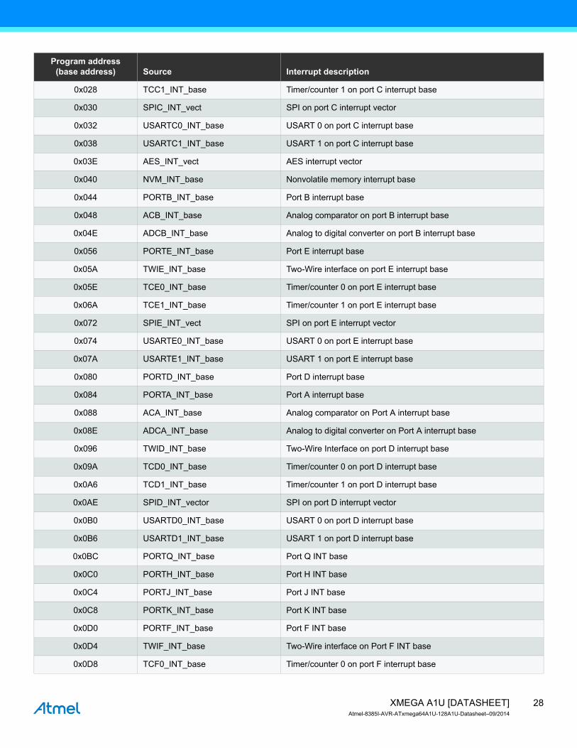
14.3 Interrupt vectorsThe interrupt vector is the sum of the peripheral’s base interrupt address and the offset address for specific interrupts in each peripheral. The base addresses for the Atmel AVR XMEGA A1U devices are shown in Table 14-1 on page 27. Offset addresses for each interrupt available in the peripheral are described for each peripheral in the XMEGA AU manual. For peripherals or modules that have only one interrupt, the interrupt vector is shown in Table 14-1 on page 27. The program address is the word address.
Table 14-1. Reset and interrupt vectors.
Program address(base address) Source Interrupt description
0x000 RESET
0x002 OSCF_INT_vect Crystal oscillator failure interrupt vector (NMI)
0x004 PORTC_INT_base Port C interrupt base
0x008 PORTR_INT_base Port R interrupt base
0x00C DMA_INT_base DMA controller interrupt base
0x014 RTC_INT_base Real time counter interrupt base
0x018 TWIC_INT_base Two-Wire interface on port C interrupt base
0x01C TCC0_INT_base Timer/counter 0 on port C interrupt base
28XMEGA A1U [DATASHEET]Atmel-8385I-AVR-ATxmega64A1U-128A1U-Datasheet–09/2014
0x028 TCC1_INT_base Timer/counter 1 on port C interrupt base
0x030 SPIC_INT_vect SPI on port C interrupt vector
0x032 USARTC0_INT_base USART 0 on port C interrupt base
0x038 USARTC1_INT_base USART 1 on port C interrupt base
0x03E AES_INT_vect AES interrupt vector
0x040 NVM_INT_base Nonvolatile memory interrupt base
0x044 PORTB_INT_base Port B interrupt base
0x048 ACB_INT_base Analog comparator on port B interrupt base
0x04E ADCB_INT_base Analog to digital converter on port B interrupt base
0x056 PORTE_INT_base Port E interrupt base
0x05A TWIE_INT_base Two-Wire interface on port E interrupt base
0x05E TCE0_INT_base Timer/counter 0 on port E interrupt base
0x06A TCE1_INT_base Timer/counter 1 on port E interrupt base
0x072 SPIE_INT_vect SPI on port E interrupt vector
0x074 USARTE0_INT_base USART 0 on port E interrupt base
0x07A USARTE1_INT_base USART 1 on port E interrupt base
0x080 PORTD_INT_base Port D interrupt base
0x084 PORTA_INT_base Port A interrupt base
0x088 ACA_INT_base Analog comparator on Port A interrupt base
0x08E ADCA_INT_base Analog to digital converter on Port A interrupt base
0x096 TWID_INT_base Two-Wire Interface on port D interrupt base
0x09A TCD0_INT_base Timer/counter 0 on port D interrupt base
0x0A6 TCD1_INT_base Timer/counter 1 on port D interrupt base
0x0AE SPID_INT_vector SPI on port D interrupt vector
0x0B0 USARTD0_INT_base USART 0 on port D interrupt base
0x0B6 USARTD1_INT_base USART 1 on port D interrupt base
0x0BC PORTQ_INT_base Port Q INT base
0x0C0 PORTH_INT_base Port H INT base
0x0C4 PORTJ_INT_base Port J INT base
0x0C8 PORTK_INT_base Port K INT base
0x0D0 PORTF_INT_base Port F INT base
0x0D4 TWIF_INT_base Two-Wire interface on Port F INT base
0x0D8 TCF0_INT_base Timer/counter 0 on port F interrupt base
Program address(base address) Source Interrupt description
29XMEGA A1U [DATASHEET]Atmel-8385I-AVR-ATxmega64A1U-128A1U-Datasheet–09/2014
0x0E4 TCF1_INT_base Timer/counter 1 on port F interrupt base
0x0EC SPIF_INT_vector SPI ion port F interrupt base
0x0EE USARTF0_INT_base USART 0 on port F interrupt base
0x0F4 USARTF1_INT_base USART 1 on port F interrupt base
0x0FA USB_INT_base USB on port D interrupt base
Program address(base address) Source Interrupt description
30XMEGA A1U [DATASHEET]Atmel-8385I-AVR-ATxmega64A1U-128A1U-Datasheet–09/2014
15. I/O Ports
15.1 Featuresz 78 General purpose input and output pins with individual configurationz Output driver with configurable driver and pull settings:
z Totem-polez Wired-ANDz Wired-ORz Bus-keeperz Inverted I/O
z Input with synchronous and/or asynchronous sensing with interrupts and eventsz Sense both edgesz Sense rising edgesz Sense falling edgesz Sense low level
z Optional pull-up and pull-down resistor on input and Wired-OR/AND configurationsz Optional slew rate controlz Asynchronous pin change sensing that can wake the device from all sleep modesz Two port interrupts with pin masking per I/O portz Efficient and safe access to port pins
z Hardware read-modify-write through dedicated toggle/clear/set registersz Configuration of multiple pins in a single operationz Mapping of port registers into bit-accessible I/O memory space
z Peripheral clocks output on port pinz Real-time counter clock output to port pinz Event channels can be output on port pinz Remapping of digital peripheral pin functions
z Selectable USART, SPI, and timer/counter input/output pin locations
15.2 OverviewOne port consists of up to eight port pins: pin 0 to 7. Each port pin can be configured as input or output with configurable driver and pull settings. They also implement synchronous and asynchronous input sensing with interrupts and events for selectable pin change conditions. Asynchronous pin-change sensing means that a pin change can wake the device from all sleep modes, included the modes where no clocks are running.
All functions are individual and configurable per pin, but several pins can be configured in a single operation. The pins have hardware read-modify-write (RMW) functionality for safe and correct change of drive value and/or pull resistor configuration. The direction of one port pin can be changed without unintentionally changing the direction of any other pin.
The port pin configuration also controls input and output selection of other device functions. It is possible to have both the peripheral clock and the real-time clock output to a port pin, and available for external use. The same applies to events from the event system that can be used to synchronize and control external functions. Other digital peripherals, such as USART, SPI, and timer/counters, can be remapped to selectable pin locations in order to optimize pin-out versus application needs.
The notation of these ports are PORTA, PORTB, PORTC, PORTD, PORTE, PORTF, PORTH, PORTJ, PORTK, PORTQ and PORTR.
31XMEGA A1U [DATASHEET]Atmel-8385I-AVR-ATxmega64A1U-128A1U-Datasheet–09/2014
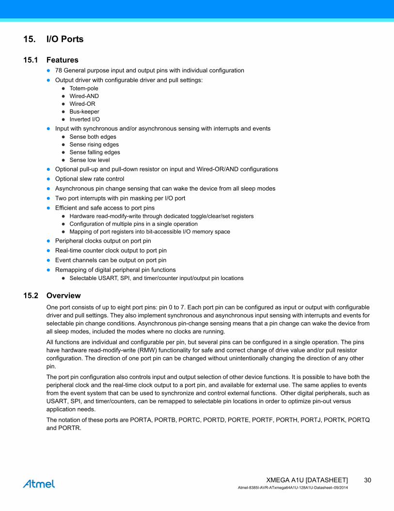
15.3 Output DriverAll port pins (Pn) have programmable output configuration. The port pins also have configurable slew rate limitation to reduce electromagnetic emission.
15.3.1 Push-pull
Figure 15-1. I/O configuration - Totem-pole.
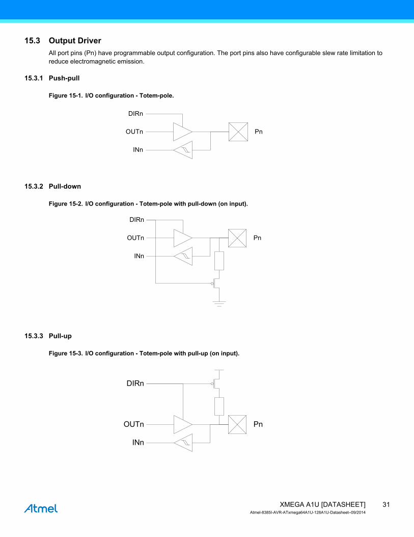
15.3.2 Pull-down
Figure 15-2. I/O configuration - Totem-pole with pull-down (on input).
15.3.3 Pull-up
Figure 15-3. I/O configuration - Totem-pole with pull-up (on input).
INn
OUTn
DIRn
Pn
INn
OUTn
DIRn
Pn
INn
OUTn
DIRn
Pn
32XMEGA A1U [DATASHEET]Atmel-8385I-AVR-ATxmega64A1U-128A1U-Datasheet–09/2014
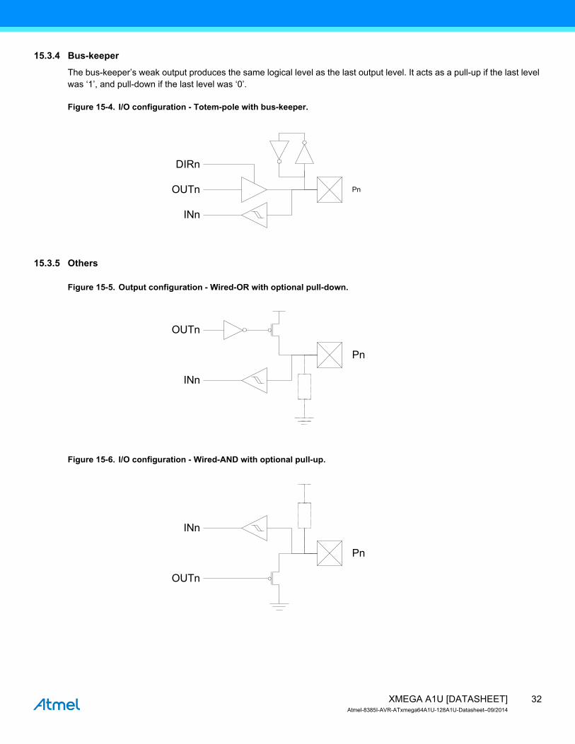
15.3.4 Bus-keeper
The bus-keeper’s weak output produces the same logical level as the last output level. It acts as a pull-up if the last level was ‘1’, and pull-down if the last level was ‘0’.
Figure 15-4. I/O configuration - Totem-pole with bus-keeper.
15.3.5 Others
Figure 15-5. Output configuration - Wired-OR with optional pull-down.
Figure 15-6. I/O configuration - Wired-AND with optional pull-up.
INn
OUTn
DIRn
Pn
INn
OUTn
Pn
INn
OUTn
Pn
33XMEGA A1U [DATASHEET]Atmel-8385I-AVR-ATxmega64A1U-128A1U-Datasheet–09/2014
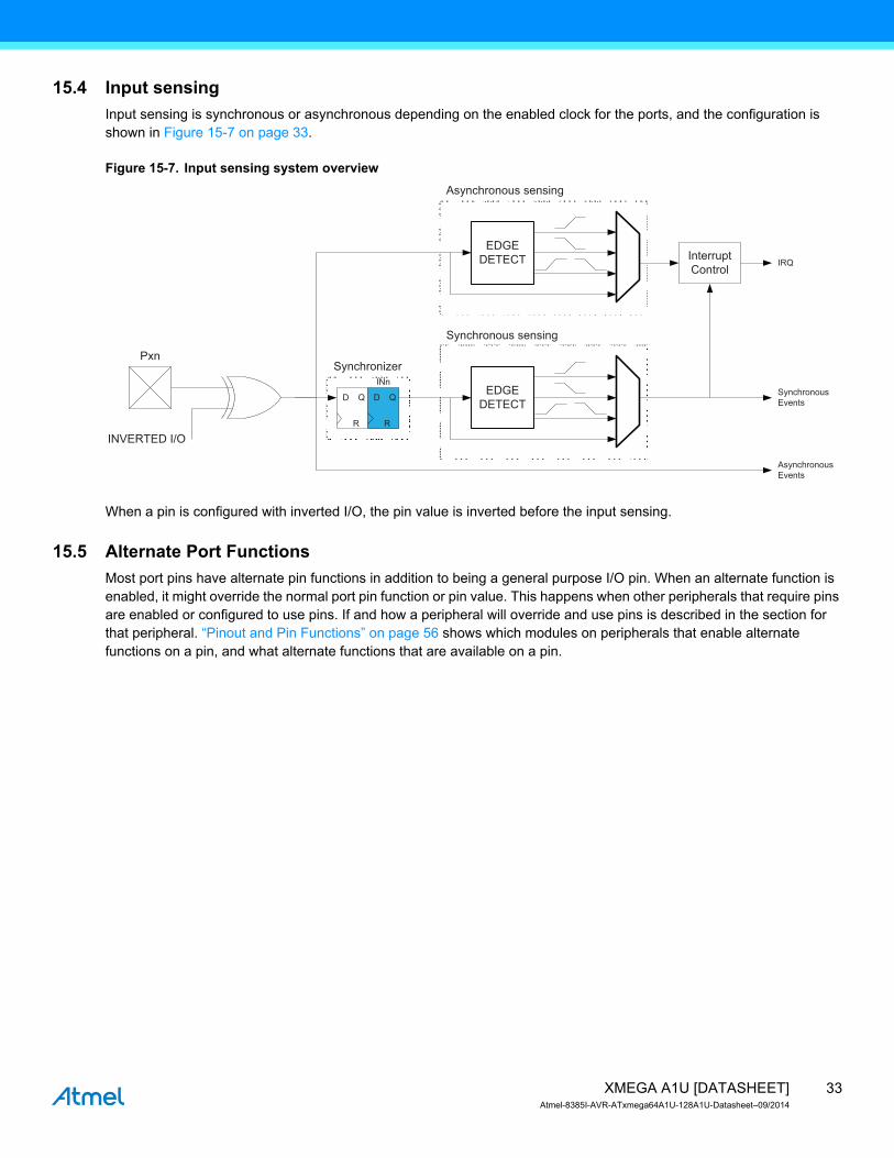
15.4 Input sensingInput sensing is synchronous or asynchronous depending on the enabled clock for the ports, and the configuration is shown in Figure 15-7 on page 33.
Figure 15-7. Input sensing system overview
When a pin is configured with inverted I/O, the pin value is inverted before the input sensing.
15.5 Alternate Port FunctionsMost port pins have alternate pin functions in addition to being a general purpose I/O pin. When an alternate function is enabled, it might override the normal port pin function or pin value. This happens when other peripherals that require pins are enabled or configured to use pins. If and how a peripheral will override and use pins is described in the section for that peripheral. “Pinout and Pin Functions” on page 56 shows which modules on peripherals that enable alternate functions on a pin, and what alternate functions that are available on a pin.
D Q
R
INVERTED I/O
InterruptControl
D Q
R
PxnSynchronizer
INnEDGE
DETECT
Synchronous sensing
EDGEDETECT
Asynchronous sensing
IRQ
Synchronous Events
Asynchronous Events
34XMEGA A1U [DATASHEET]Atmel-8385I-AVR-ATxmega64A1U-128A1U-Datasheet–09/2014
16. TC0/1 – 16-bit Timer/Counter Type 0 and 1
16.1 Featuresz Eight 16-bit timer/counters
z Four timer/counters of type 0z Four timer/counters of type 1
z 32-bit timer/counter support by cascading two timer/countersz Up to four compare or capture (CC) channels
z Four CC channels for timer/counters of type 0z Two CC channels for timer/counters of type 1
z Double buffered timer period setting z Double buffered capture or compare channelsz Waveform generation:
z Frequency generationz Single-slope pulse width modulationz Dual-slope pulse width modulation
z Input capture:z Input capture with noise cancellingz Frequency capturez Pulse width capturez 32-bit input capture
z Timer overflow and error interrupt eventsz One compare match or input capture interrupt event per CC channelz Can be used with event system for:
z Quadrature decodingz Count and direction controlz Capture
z Can be used with DMA and trigger DMA transactions z High-resolution extension
z Increases frequency and waveform resolution by 4x (2-bit) or 8x (3-bit)z Advanced waveform extension
z Low and high-side output with programmable dead-time insertion (DTI)z Event controlled fault protection for safe disabling of external drivers
16.2 OverviewAtmel AVR XMEGA devices have a set of eight flexible 16-bit timer/counters (TC). Their capabilities include accurate program execution timing, frequency and waveform generation, and input capture with time and frequency measurement of digital signals. Two timer/counters can be cascaded to create a 32-bit timer/counter with optional 32-bit capture.
A timer/counter consists of a base counter and a set of compare or capture (CC) channels. The base counter can be used to count clock cycles or events. It has direction control and period setting that can be used for timing. The CC channels can be used together with the base counter to do compare match control, frequency generation, and pulse width waveform modulation, as well as various input capture operations. A timer/counter can be configured for either capture or compare functions, but cannot perform both at the same time.
A timer/counter can be clocked and timed from the peripheral clock with optional prescaling or from the event system. The event system can also be used for direction control and capture trigger or to synchronize operations.
There are two differences between timer/counter type 0 and type 1. Timer/counter 0 has four CC channels, and timer/counter 1 has two CC channels. All information related to CC channels 3 and 4 is valid only for timer/counter 0. Only Timer/Counter 0 has the split mode feature that split it into 2 8-bit Timer/Counters with four compare channels each.
35XMEGA A1U [DATASHEET]Atmel-8385I-AVR-ATxmega64A1U-128A1U-Datasheet–09/2014
Some timer/counters have extensions to enable more specialized waveform and frequency generation. The advanced waveform extension (AWeX) is intended for motor control and other power control applications. It enables low- and high-side output with dead-time insertion, as well as fault protection for disabling and shutting down external drivers. It can also generate a synchronized bit pattern across the port pins.
The advanced waveform extension can be enabled to provide extra and more advanced features for the Timer/Counter. This is only available for Timer/Counter 0. See ”“AWeX – Advanced Waveform Extension” on page 37 for more details.
The high-resolution (hi-res) extension can be used to increase the waveform output resolution by four or eight times by using an internal clock source running up to four times faster than the peripheral clock. See “Hi-Res – High Resolution Extension” on page 38 for more details.
Figure 16-1. Overview of a timer/counter (TC) and closely related peripherals.
PORTC, PORTD, PORTE and PORTF each has one timer/counter 0 and one timer/counter1. Notation of these timer/counters are TCC0 (timer/counter C0), TCC1, TCD0, TCD1, TCE0, TCE1, TCF0, and TCF1, respectively.
AWeX
Compare/Capture Channel DCompare/Capture Channel C
Compare/Capture Channel BCompare/Capture Channel A
Waveform GenerationBuffer
Comparator Hi-R
es
Fault Protection
Capture Control
Base Counter
CounterControl Logic
Timer PeriodPrescaler
Dead-Time Insertion
Pattern Generation
clkPER4
PORT
Event System
clkPER
Timer/Counter
36XMEGA A1U [DATASHEET]Atmel-8385I-AVR-ATxmega64A1U-128A1U-Datasheet–09/2014
17. TC2 – Time/Counter Type 2
17.1 Featuresz Eight eight-bit timer/counters
z Four Low-byte timer/countersz Four High-byte timer/counters
z Up to eight compare channels in each timer/counter 2z Four compare channels for the low-byte timer/counterz Four compare channels for the high-byte timer/counter
z Waveform generationz Single slope pulse width modulation
z Timer underflow interrupts/eventsz One compare match interrupt/event per compare channel for the low-byte timer/counterz Can be used with the event system for count controlz Can be used to trigger DMA transactions
17.2 OverviewThere are four Timer/counter 2. These are realized when a Timer/counter 0 is set in split mode. It is then a system of two eight-bit timer/counters, each with four compare channels. This results in eight configurable pulse width modulation (PWM) channels with individually controlled duty cycles, and is intended for applications that require a high number of PWM channels.
The two eight-bit timer/counters in this system are referred to as the low-byte timer/counter and high-byte timer/counter, respectively. The difference between them is that only the low-byte timer/counter can be used to generate compare match interrupts, events and DMA triggers.
The two eight-bit timer/counters have a shared clock source and separate period and compare settings. They can be clocked and timed from the peripheral clock, with optional prescaling, or from the event system. The counters are always counting down.
PORTC, PORTD, PORTE and PORTF each has one Timer/Counter 2. Notation of these are TCC2 (Time/Counter C2), TCD2, TCE2 and TCF2, respectively.
37XMEGA A1U [DATASHEET]Atmel-8385I-AVR-ATxmega64A1U-128A1U-Datasheet–09/2014
18. AWeX – Advanced Waveform Extension
18.1 Featuresz Waveform output with complementary output from each compare channelz Four dead-time insertion (DTI) units
z 8-bit resolutionz Separate high and low side dead-time settingz Double buffered dead timez Optionally halts timer during dead-time insertion
z Pattern generation unit creating synchronised bit pattern across the port pinsz Double buffered pattern generationz Optional distribution of one compare channel output across the port pins
z Event controlled fault protection for instant and predictable fault triggering
18.2 OverviewThe advanced waveform extension (AWeX) provides extra functions to the timer/counter in waveform generation (WG) modes. It is primarily intended for use with different types of motor control and other power control applications. It enables low- and high side output with dead-time insertion and fault protection for disabling and shutting down external drivers. It can also generate a synchronized bit pattern across the port pins.
Each of the waveform generator outputs from the Timer/Counter 0 are split into a complimentary pair of outputs when any AWeX features are enabled. These output pairs go through a dead-time insertion (DTI) unit that generates the non-inverted low side (LS) and inverted high side (HS) of the WG output with dead-time insertion between LS and HS switching. The DTI output will override the normal port value according to the port override setting.
The pattern generation unit can be used to generate a synchronized bit pattern on the port it is connected to. In addition, the WG output from compare channel A can be distributed to and override all the port pins. When the pattern generator unit is enabled, the DTI unit is bypassed.
The fault protection unit is connected to the event system, enabling any event to trigger a fault condition that will disable the AWeX output. The event system ensures predictable and instant fault reaction, and gives great flexibility in the selection of fault triggers.
The AWeX is available for TCC0 and TCE0. The notation of these are AWEXC and AWEXE.
38XMEGA A1U [DATASHEET]Atmel-8385I-AVR-ATxmega64A1U-128A1U-Datasheet–09/2014
19. Hi-Res – High Resolution Extension
19.1 Featuresz Increases waveform generator resolution up to 8x (three bits)z Supports frequency, single-slope PWM and dual-slope PWM generationz Supports the AWeX when this is used for the same timer/counter
19.2 OverviewThe high-resolution (hi-res) extension can be used to increase the resolution of the waveform generation output from a timer/counter by four or eight. It can be used for a timer/counter doing frequency, single-slope PWM, or dual-slope PWM generation. It can also be used with the AWeX if this is used for the same timer/counter.
The hi-res extension uses the peripheral 4x clock (ClkPER4). The system clock prescalers must be configured so the peripheral 4x clock frequency is four times higher than the peripheral and CPU clock frequency when the hi-res extension is enabled.
There are four hi-res extensions that each can be enabled for each timer/counters pair on PORTC, PORTD, PORTE and PORTF. The notation of these peripherals are HIRESC, HIRESD, HIRESE and HIRESF, respectively.
39XMEGA A1U [DATASHEET]Atmel-8385I-AVR-ATxmega64A1U-128A1U-Datasheet–09/2014
20. RTC – 16-bit Real-Time Counter
20.1 Featuresz 16-bit resolutionz Selectable clock source
z 32.768kHz external crystalz External clockz 32.768kHz internal oscillatorz 32kHz internal ULP oscillator
z Programmable 10-bit clock prescalingz One compare registerz One period registerz Clear counter on period overflow z Optional interrupt/event on overflow and compare match
20.2 OverviewThe 16-bit real-time counter (RTC) is a counter that typically runs continuously, including in low-power sleep modes, to keep track of time. It can wake up the device from sleep modes and/or interrupt the device at regular intervals.
The reference clock is typically the 1.024kHz output from a high-accuracy crystal of 32.768kHz, and this is the configuration most optimized for low power consumption. The faster 32.768kHz output can be selected if the RTC needs a resolution higher than 1ms. The RTC can also be clocked from an external clock signal, the 32.768kHz internal oscillator or the 32kHz internal ULP oscillator.
The RTC includes a 10-bit programmable prescaler that can scale down the reference clock before it reaches the counter. A wide range of resolutions and time-out periods can be configured. With a 32.768kHz clock source, the maximum resolution is 30.5µs, and time-out periods can range up to 2000 seconds. With a resolution of 1s, the maximum timeout period is more than18 hours (65536 seconds). The RTC can give a compare interrupt and/or event when the counter equals the compare register value, and an overflow interrupt and/or event when it equals the period register value.
Figure 20-1. Real-time counter overview.
32.768kHz Crystal Osc
32.768kHz Int. Osc
TOSC1
TOSC2
External Clock
DIV32
DIV32
32kHz int ULP (DIV32)
RTCSRC
10-bitprescaler
clkRTC
CNT
PER
COMP
=
=
”match”/Compare
TOP/Overflow
40XMEGA A1U [DATASHEET]Atmel-8385I-AVR-ATxmega64A1U-128A1U-Datasheet–09/2014
21. USB – Universal Serial Bus Interface
21.1 Featuresz One USB 2.0 full speed (12Mbps) and low speed (1.5Mbps) device compliant interfacez Integrated on-chip USB transceiver, no external components neededz 16 endpoint addresses with full endpoint flexibility for up to 31 endpoints
z One input endpoint per endpoint addressz One output endpoint per endpoint address
z Endpoint address transfer type selectable toz Control transfersz Interrupt transfersz Bulk transfersz Isochronous transfers
z Configurable data payload size per endpoint, up to 1023 bytesz Endpoint configuration and data buffers located in internal SRAM
z Configurable location for endpoint configuration dataz Configurable location for each endpoint's data buffer
z Built-in direct memory access (DMA) to internal SRAM for:z Endpoint configurationsz Reading and writing endpoint data
z Ping-pong operation for higher throughput and double buffered operation z Input and output endpoint data buffers used in a single directionz CPU/DMA controller can update data buffer during transfer
z Multi packet transfer for reduced interrupt load and software interventionz Data payload exceeding maximum packet size is transferred in one continuous transferz No interrupts or software interaction on packet transaction level
z Transaction complete FIFO for workflow management when using multiple endpointsz Tracks all completed transactions in a first-come, first-served work queue
z Clock selection independent of system clock source and selectionz Minimum 1.5MHz CPU clock required for low speed USB operationz Minimum 12MHz CPU clock required for full speed operationz Connection to event systemz On chip debug possibilities during USB transactions
21.2 OverviewThe USB module is a USB 2.0 full speed (12Mbps) and low speed (1.5Mbps) device compliant interface.
The USB supports 16 endpoint addresses. All endpoint addresses have one input and one output endpoint, for a total of 31 configurable endpoints and one control endpoint. Each endpoint address is fully configurable and can be configured for any of the four transfer types; control, interrupt, bulk, or isochronous. The data payload size is also selectable, and it supports data payloads up to 1023 bytes.
No dedicated memory is allocated for or included in the USB module. Internal SRAM is used to keep the configuration for each endpoint address and the data buffer for each endpoint. The memory locations used for endpoint configurations and data buffers are fully configurable. The amount of memory allocated is fully dynamic, according to the number of endpoints in use and the configuration of these. The USB module has built-in direct memory access (DMA), and will read/write data from/to the SRAM when a USB transaction takes place.
To maximize throughput, an endpoint address can be configured for ping-pong operation. When done, the input and output endpoints are both used in the same direction. The CPU or DMA controller can then read/write one data buffer while the USB module writes/reads the others, and vice versa. This gives double buffered communication.
41XMEGA A1U [DATASHEET]Atmel-8385I-AVR-ATxmega64A1U-128A1U-Datasheet–09/2014
Multipacket transfer enables a data payload exceeding the maximum packet size of an endpoint to be transferred as multiple packets without software intervention. This reduces the CPU intervention and the interrupts needed for USB transfers.
For low-power operation, the USB module can put the microcontroller into any sleep mode when the USB bus is idle and a suspend condition is given. Upon bus resumes, the USB module can wake up the microcontroller from any sleep mode.
PORTD has one USB. Notation of this is USB.
42XMEGA A1U [DATASHEET]Atmel-8385I-AVR-ATxmega64A1U-128A1U-Datasheet–09/2014
22. TWI – Two-Wire Interface
22.1 Featuresz Four identical two-wire interface peripheralsz Bidirectional two-wire communication interface
z Phillips I2C compatiblez System Management Bus (SMBus) compatible
z Bus master and slave operation supportedz Slave operationz Single bus master operationz Bus master in multi-master bus environmentz Multi-master arbitration
z Flexible slave address match functionsz 7-bit and general call address recognition in hardwarez 10-bit addressing supportedz Address mask register for dual address match or address range maskingz Optional software address recognition for unlimited number of addresses
z Slave can operate in all sleep modes, including power-downz Slave address match can wake device from all sleep modes, including power-downz 100kHz and 400kHz bus frequency support z Slew-rate limited output driversz Input filter for bus noise and spike suppressionz Support arbitration between start repeated start and data bit (SMBus)z Slave arbitration allows support for address resolve protocol (ARP) (SMBus)
22.2 OverviewThe two-wire interface (TWI) is a bidirectional, two-wire communication interface. It is I2C and System Management Bus (SMBus) compatible. The only external hardware needed to implement the bus is one pull-up resistor on each bus line.
A device connected to the bus must act as a master or a slave. The master initiates a data transaction by addressing a slave on the bus and telling whether it wants to transmit or receive data. One bus can have many slaves and one or several masters that can take control of the bus. An arbitration process handles priority if more than one master tries to transmit data at the same time. Mechanisms for resolving bus contention are inherent in the protocol.
The TWI module supports master and slave functionality. The master and slave functionality are separated from each other, and can be enabled and configured separately. The master module supports multi-master bus operation and arbitration. It contains the baud rate generator. Both 100kHz and 400kHz bus frequencies are supported. Quick command and smart mode can be enabled to auto-trigger operations and reduce software complexity.
The slave module implements 7-bit address match and general address call recognition in hardware. 10-bit addressing is also supported. A dedicated address mask register can act as a second address match register or as a register for address range masking. The slave continues to operate in all sleep modes, including power-down mode. This enables the slave to wake up the device from all sleep modes on TWI address match. It is possible to disable the address matching to let this be handled in software instead.
The TWI module will detect START and STOP conditions, bus collisions, and bus errors. Arbitration lost, errors, collision, and clock hold on the bus are also detected and indicated in separate status flags available in both master and slave modes.
It is possible to disable the TWI drivers in the device, and enable a four-wire digital interface for connecting to an external TWI bus driver. This can be used for applications where the device operates from a different VCC voltage than used by the TWI bus.
43XMEGA A1U [DATASHEET]Atmel-8385I-AVR-ATxmega64A1U-128A1U-Datasheet–09/2014
PORTC, PORTD, PORTE, and PORTF each has one TWI. Notation of these peripherals are TWIC, TWID, TWIE, and TWIF.
23. SPI – Serial Peripheral Interface
23.1 Featuresz Four identical SPI peripheralsz Full-duplex, three-wire synchronous data transferz Master or slave operationz Lsb first or msb first data transferz Eight programmable bit ratesz Interrupt flag at the end of transmissionz Write collision flag to indicate data collisionz Wake up from idle sleep modez Double speed master mode
23.2 OverviewThe Serial Peripheral Interface (SPI) is a high-speed synchronous data transfer interface using three or four pins. It allows fast communication between an Atmel AVR XMEGA device and peripheral devices or between several microcontrollers. The SPI supports full-duplex communication.
A device connected to the bus must act as a master or slave. The master initiates and controls all data transactions.
PORTC, PORTD, PORTE, and PORTF each has one SPI. Notation of these peripherals are SPIC, SPID, SPIE, and SPIF.
44XMEGA A1U [DATASHEET]Atmel-8385I-AVR-ATxmega64A1U-128A1U-Datasheet–09/2014
24. USART
24.1 Featuresz Eight identical USART peripheralsz Full-duplex operationz Asynchronous or synchronous operation
z Synchronous02 clock rates up to 1/2 of the device clock frequencyz Asynchronous clock rates up to 1/8 of the device clock frequency
z Supports serial frames with 5, 6, 7, 8, or 9 data bits and 1 or 2 stop bitsz Fractional baud rate generator
z Can generate desired baud rate from any system clock frequencyz No need for external oscillator with certain frequencies
z Built-in error detection and correction schemes z Odd or even parity generation and parity check z Data overrun and framing error detectionz Noise filtering includes false start bit detection and digital low-pass filter
z Separate interrupts forz Transmit completez Transmit data register emptyz Receive complete
z Multiprocessor communication modez Addressing scheme to address a specific devices on a multi device busz Enable unaddressed devices to automatically ignore all frames
z Master SPI modez Double buffered operationz Operation up to 1/2 of the peripheral clock frequency
z IRCOM module for IrDA compliant pulse modulation/demodulation
24.2 OverviewThe universal synchronous and asynchronous serial receiver and transmitter (USART) is a fast and flexible serial communication module. The USART supports full-duplex communication and asynchronous and synchronous operation. The USART can be configured to operate in SPI master mode and used for SPI communication.
Communication is frame based, and the frame format can be customized to support a wide range of standards. The USART is buffered in both directions, enabling continued data transmission without any delay between frames. Separate interrupts for receive and transmit complete enable fully interrupt driven communication. Frame error and buffer overflow are detected in hardware and indicated with separate status flags. Even or odd parity generation and parity check can also be enabled.
The clock generator includes a fractional baud rate generator that is able to generate a wide range of USART baud rates from any system clock frequencies. This removes the need to use an external crystal oscillator with a specific frequency to achieve a required baud rate. It also supports external clock input in synchronous slave operation.
When the USART is set in master SPI mode, all USART-specific logic is disabled, leaving the transmit and receive buffers, shift registers, and baud rate generator enabled. Pin control and interrupt generation are identical in both modes. The registers are used in both modes, but their functionality differs for some control settings.
An IRCOM module can be enabled for one USART to support IrDA 1.4 physical compliant pulse modulation and demodulation for baud rates up to 115.2Kbps.
PORTC, PORTD, PORTE, and PORTF each has two USARTs. Notation of these peripherals are USARTC0, USARTC1, USARTD0, USARTD1, USARTE0, USARTE1, USARTF0 and USARTF1.
45XMEGA A1U [DATASHEET]Atmel-8385I-AVR-ATxmega64A1U-128A1U-Datasheet–09/2014
25. IRCOM – IR Communication Module
25.1 Featuresz Pulse modulation/demodulation for infrared communicationz IrDA compatible for baud rates up to 115.2Kbpsz Selectable pulse modulation scheme
z 3/16 of the baud rate periodz Fixed pulse period, 8-bit programmablez Pulse modulation disabled
z Built-in filteringz Can be connected to and used by any USART
25.2 OverviewAtmel AVR XMEGA devices contain an infrared communication module (IRCOM) that is IrDA compatible for baud rates up to 115.2Kbps. It can be connected to any USART to enable infrared pulse encoding/decoding for that USART.
46XMEGA A1U [DATASHEET]Atmel-8385I-AVR-ATxmega64A1U-128A1U-Datasheet–09/2014
26. AES and DES Crypto Engine
26.1 Featuresz Data Encryption Standard (DES) CPU instructionz Advanced Encryption Standard (AES) crypto modulez DES Instruction
z Encryption and decryptionz DES supportedz Encryption/decryption in 16 CPU clock cycles per 8-byte block
z AES crypto modulez Encryption and decryptionz Supports 128-bit keysz Supports XOR data load mode to the state memoryz Encryption/decryption in 375 clock cycles per 16-byte block
26.2 OverviewThe Advanced Encryption Standard (AES) and Data Encryption Standard (DES) are two commonly used standards for cryptography. These are supported through an AES peripheral module and a DES CPU instruction, and the communication interfaces and the CPU can use these for fast, encrypted communication and secure data storage.
DES is supported by an instruction in the AVR CPU. The 8-byte key and 8-byte data blocks must be loaded into the register file, and then the DES instruction must be executed 16 times to encrypt/decrypt the data block.
The AES crypto module encrypts and decrypts 128-bit data blocks with the use of a 128-bit key. The key and data must be loaded into the key and state memory in the module before encryption/decryption is started. It takes 375 peripheral clock cycles before the encryption/decryption is done. The encrypted/encrypted data can then be read out, and an optional interrupt can be generated. The AES crypto module also has DMA support with transfer triggers when encryption/decryption is done and optional auto-start of encryption/decryption when the state memory is fully loaded.
47XMEGA A1U [DATASHEET]Atmel-8385I-AVR-ATxmega64A1U-128A1U-Datasheet–09/2014
27. CRC – Cyclic Redundancy Check Generator
27.1 Featuresz Cyclic redundancy check (CRC) generation and checking for
z Communication dataz Program or data in flash memoryz Data in SRAM and I/O memory space
z Integrated with flash memory, DMA controller and CPUz Continuous CRC on data going through a DMA channelz Automatic CRC of the complete or a selectable range of the flash memoryz CPU can load data to the CRC generator through the I/O interface
z CRC polynomial software selectable toz CRC-16 (CRC-CCITT)z CRC-32 (IEEE 802.3)
z Zero remainder detection
27.2 OverviewA cyclic redundancy check (CRC) is an error detection technique test algorithm used to find accidental errors in data, and it is commonly used to determine the correctness of a data transmission, and data present in the data and program memories. A CRC takes a data stream or a block of data as input and generates a 16- or 32-bit output that can be appended to the data and used as a checksum. When the same data are later received or read, the device or application repeats the calculation. If the new CRC result does not match the one calculated earlier, the block contains a data error. The application will then detect this and may take a corrective action, such as requesting the data to be sent again or simply not using the incorrect data.
Typically, an n-bit CRC applied to a data block of arbitrary length will detect any single error burst not longer than n bits (any single alteration that spans no more than n bits of the data), and will detect the fraction 1-2-n of all longer error bursts. The CRC module in Atmel AVR XMEGA devices supports two commonly used CRC polynomials; CRC-16 (CRC-CCITT) and CRC-32 (IEEE 802.3).z CRC-16:
z CRC-32:
Polynomial: x16+x12+x5+1
Hex value: 0x1021
Polynomial: x32+x26+x23+x22+x16+x12+x11+x10+x8+x7+x5+x4+x2+x+1
Hex value: 0x04C11DB7
48XMEGA A1U [DATASHEET]Atmel-8385I-AVR-ATxmega64A1U-128A1U-Datasheet–09/2014
28. EBI – External Bus Interface
28.1 Featuresz Supports SRAM up to:
z 512KB using 2- or 3-port EBI configurationz 16MB using 3- or 4-port EBI configuration
z Supports SDRAM up to:z 128Mb using 3- or 4-port EBI configurationz 4-bit SDRAM with 3-port EBI configurationz 4- or 8-bit SDRAM with 4-port EBI configuration
z Four software configurable chip selectsz Software configurable wait state insertionz Can run from the 2x peripheral clock frequency for fast accessz Simultaneous SRAM and SDRAM support with 4-port EBI configuration
28.2 OverviewThe External Bus Interface (EBI) is used to connect external peripherals and memory for accessthrough the data memory space. When the EBI is enabled, data address space outside the internal SRAM becomes available using dedicated EBI pins.
The EBI can interface external SRAM, SDRAM, and peripherals, such as LCD displays and other memory mapped devices.
The address space for the external memory is selectable from 256 bytes (8-bit) up to 16MB (24-bit). Various multiplexing modes for address and data lines can be selected for optimal use of pins when more or fewer pins are available for the EBI. The complete memory will be mapped into one linear data address space continuing from the end of the internal SRAM.
The EBI has four chip selects, each with separate configuration. Each can be configured for SRAM, SRAM low pin count (LPC), or SDRAM.
The EBI is clocked from the fast, 2x peripheral clock, running up to two times faster than the CPU.
Four-bit and eight-bit SDRAM are supported, and SDRAM configurations, such as CAS latency and refresh rate, are configurable in software.
49XMEGA A1U [DATASHEET]Atmel-8385I-AVR-ATxmega64A1U-128A1U-Datasheet–09/2014
29. ADC – 12-bit Analog to Digital Converter
29.1 Featuresz Two Analog to Digital Convertersz 12-bit resolutionz Up to two million samples per second
z Two inputs can be sampled simultaneously using ADC and 1x gain stagez Four inputs can be sampled within 1.5µsz Down to 2.5µs conversion time with 8-bit resolutionz Down to 3.5µs conversion time with 12-bit resolution
z Differential and single-ended inputz Up to 16 single-ended inputsz 16x4 differential inputs without gainz 8x4 differential input with gain
z Built-in differential gain stagez 1/2x, 1x, 2x, 4x, 8x, 16x, 32x, and 64x gain options
z Single, continuous and scan conversion optionsz Four internal inputs
z Internal temperature sensorz DAC outputz AVCC voltage divided by 10z 1.1V bandgap voltage
z Four conversion channels with individual input control and result registersz Enable four parallel configurations and results
z Internal and external reference optionsz Compare function for accurate monitoring of user defined thresholdsz Optional event triggered conversion for accurate timingz Optional DMA transfer of conversion resultsz Optional interrupt/event on compare result
29.2 OverviewThe ADC converts analog signals to digital values. There are two Analog to Digital Converters (ADCs) modules that can be operated simultaneously, individually or synchronized.
The ADC has 12-bit resolution and is capable of converting up to two million samples per second (msps). The input selection is flexible, and both single-ended and differential measurements can be done. For differential measurements, an optional gain stage is available to increase the dynamic range. In addition, several internal signal inputs are available. The ADC can provide both signed and unsigned results.
This is a pipelined ADC that consists of several consecutive stages. The pipelined design allows a high sample rate at a low system clock frequency. It also means that a new input can be sampled and a new ADC conversion started while other ADC conversions are still ongoing. This removes dependencies between sample rate and propagation delay.
The ADC has four conversion channels (0-3) with individual input selection, result registers, and conversion start control. The ADC can then keep and use four parallel configurations and results, and this will ease use for applications with high data throughput or for multiple modules using the ADC independently. It is possible to use DMA to move ADC results directly to memory or peripherals when conversions are done.
Both internal and external reference voltages can be used. An integrated temperature sensor is available for use with the ADC. The output from the DAC, AVCC/10 and the bandgap voltage can also be measured by the ADC.
The ADC has a compare function for accurate monitoring of user defined thresholds with minimum software intervention required.
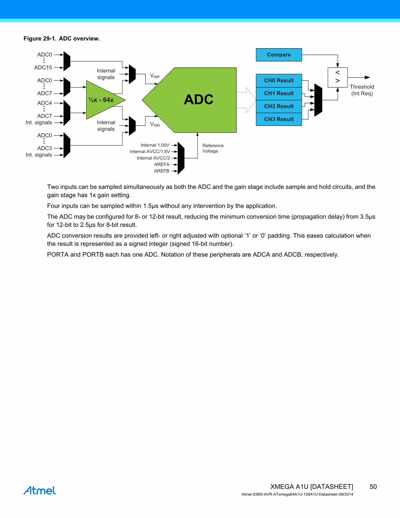
50XMEGA A1U [DATASHEET]Atmel-8385I-AVR-ATxmega64A1U-128A1U-Datasheet–09/2014
Figure 29-1. ADC overview.
Two inputs can be sampled simultaneously as both the ADC and the gain stage include sample and hold circuits, and the gain stage has 1x gain setting.
Four inputs can be sampled within 1.5µs without any intervention by the application.
The ADC may be configured for 8- or 12-bit result, reducing the minimum conversion time (propagation delay) from 3.5µs for 12-bit to 2.5µs for 8-bit result.
ADC conversion results are provided left- or right adjusted with optional ‘1’ or ‘0’ padding. This eases calculation when the result is represented as a signed integer (signed 16-bit number).
PORTA and PORTB each has one ADC. Notation of these peripherals are ADCA and ADCB, respectively.
CH1 Result
CH0 Result
CH2 Result
Compare
<>
Threshold(Int Req)
Internal 1.00VInternal AVCC/1.6V
AREFAAREFB
VINP
VINN
Internalsignals
Internal AVCC/2
Internalsignals
CH3 Result
ADC0
ADC7
ADC4
ADC7
ADC0
ADC3
•••
Int. signals
Int. signals
Reference Voltage
½x - 64x•••
•••
ADC0
ADC15
•••
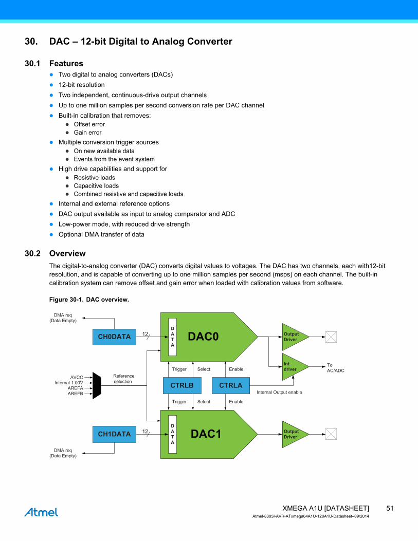
51XMEGA A1U [DATASHEET]Atmel-8385I-AVR-ATxmega64A1U-128A1U-Datasheet–09/2014
30. DAC – 12-bit Digital to Analog Converter
30.1 Featuresz Two digital to analog converters (DACs)z 12-bit resolutionz Two independent, continuous-drive output channelsz Up to one million samples per second conversion rate per DAC channelz Built-in calibration that removes:
z Offset errorz Gain error
z Multiple conversion trigger sourcesz On new available dataz Events from the event system
z High drive capabilities and support forz Resistive loadsz Capacitive loadsz Combined resistive and capacitive loads
z Internal and external reference optionsz DAC output available as input to analog comparator and ADCz Low-power mode, with reduced drive strengthz Optional DMA transfer of data
30.2 OverviewThe digital-to-analog converter (DAC) converts digital values to voltages. The DAC has two channels, each with12-bit resolution, and is capable of converting up to one million samples per second (msps) on each channel. The built-in calibration system can remove offset and gain error when loaded with calibration values from software.
Figure 30-1. DAC overview.
CTRLA
CH1DATA
CH0DATA
Trigger
Trigger
Internal Output enable
Enable
Internal 1.00VAREFAAREFB
Referenceselection
AVCC
Output Driver
Output Driver
DATA
Int.driver
DATA
CTRLB
DMA req(Data Empty)
DMA req(Data Empty)
Select
12
12
Select
EnableToAC/ADC
52XMEGA A1U [DATASHEET]Atmel-8385I-AVR-ATxmega64A1U-128A1U-Datasheet–09/2014
A DAC conversion is automatically started when new data to be converted are available. Events from the event system can also be used to trigger a conversion, and this enables synchronized and timed conversions between the DAC and other peripherals, such as a timer/counter. The DMA controller can be used to transfer data to the DAC.
The DAC has high drive strength, and is capable of driving both resistive and capacitive loads, aswell as loads which combine both. A low-power mode is available, which will reduce the drive strength of the output.
Internal and external voltage references can be used. The DAC output is also internally available for use as input to the analog comparator or ADC.
PORTA and PORTB each has one DAC. Notation of these peripherals are DACA and DACB, respectively.
53XMEGA A1U [DATASHEET]Atmel-8385I-AVR-ATxmega64A1U-128A1U-Datasheet–09/2014
31. AC – Analog Comparator
31.1 Featuresz Four Analog Comparatorsz Selectable propagation delay versus current consumptionz Selectable hysteresis
z Noz Smallz Large
z Analog comparator output available on pinz Flexible input selection
z All pins on the portz Output from the DACz Bandgap reference voltagez A 64-level programmable voltage scaler of the internal AVCC voltage
z Interrupt and event generation on:z Rising edgez Falling edgez Toggle
z Window function interrupt and event generation on:z Signal above windowz Signal inside windowz Signal below window
z Constant current source with configurable output pin selection
31.2 OverviewThe analog comparator (AC) compares the voltage levels on two inputs and gives a digital output based on this comparison. The analog comparator may be configured to generate interrupt requests and/or events upon several different combinations of input change.
Two important properties of the analog comparator’s dynamic behavior are: hysteresis and propagation delay. Both of these parameters may be adjusted in order to achieve the optimal operation for each application.
The input selection includes analog port pins, several internal signals, and a 64-level programmable voltage scaler. The analog comparator output state can also be output on a pin for use by external devices.
A constant current source can be enabled and output on a selectable pin. This can be used to replace, for example, external resistors used to charge capacitors in capacitive touch sensing applications.
The analog comparators are always grouped in pairs on each port. These are called analog comparator 0 (AC0) and analog comparator 1 (AC1). They have identical behavior, but separate control registers. Used as pair, they can be set in window mode to compare a signal to a voltage range instead of a voltage level.
PORTA and PORTB each has one AC pair. Notations are ACA and ACB, respectively.
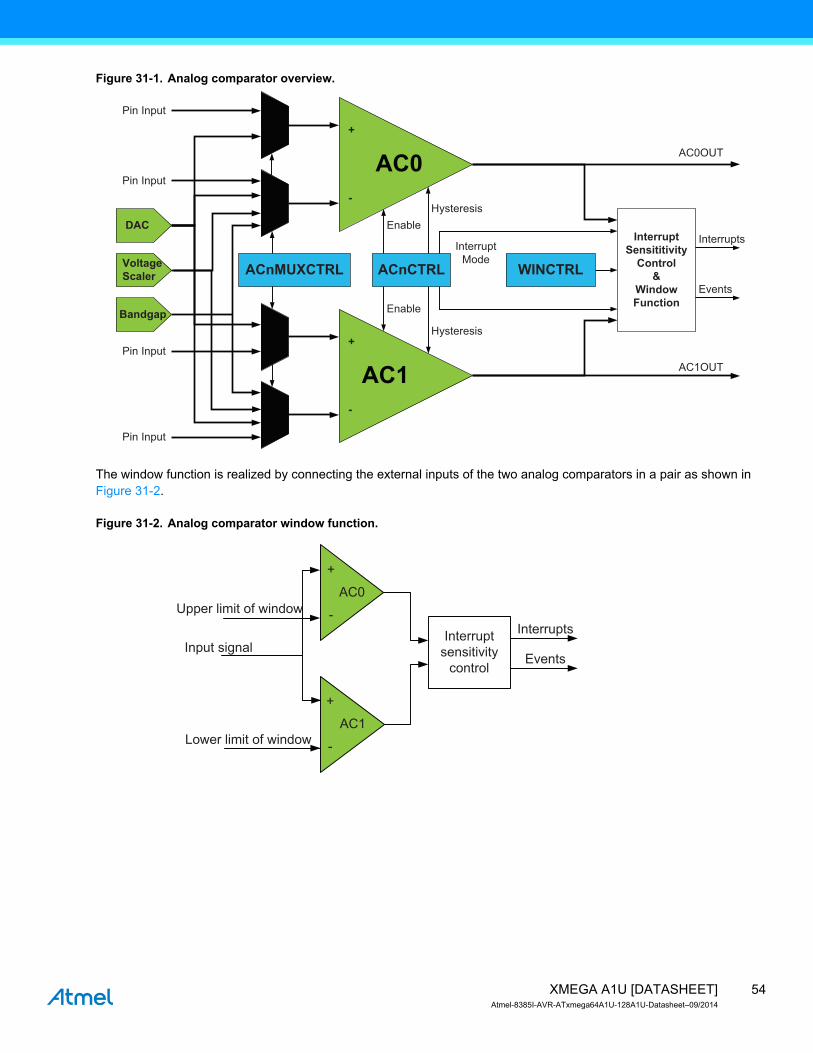
54XMEGA A1U [DATASHEET]Atmel-8385I-AVR-ATxmega64A1U-128A1U-Datasheet–09/2014
Figure 31-1. Analog comparator overview.
The window function is realized by connecting the external inputs of the two analog comparators in a pair as shown in Figure 31-2.
Figure 31-2. Analog comparator window function.
ACnMUXCTRL ACnCTRLInterrupt
Mode
Enable
Enable
Hysteresis
Hysteresis
AC1OUT
WINCTRL
Interrupt Sensititivity
Control&
WindowFunction
Events
Interrupts
AC0OUT
Pin Input
Pin Input
Pin Input
Pin Input
Voltage Scaler
DAC
Bandgap
+
-
+
-
AC0+
-
AC1+
-
Input signal
Upper limit of window
Lower limit of window
Interrupt sensitivity
control
Interrupts
Events
55XMEGA A1U [DATASHEET]Atmel-8385I-AVR-ATxmega64A1U-128A1U-Datasheet–09/2014
32. PDI – Programming and Debugging
32.1 Featuresz Programming
z External programming through PDI or JTAG interfacesz Minimal protocol overhead for fast operationz Built-in error detection and handling for reliable operation
z Boot loader support for programming through any communication interfacez Debugging
z Nonintrusive, real-time, on-chip debug systemz No software or hardware resources required from device except pin connectionz Program flow control
z Go, Stop, Reset, Step Into, Step Over, Step Out, Run-to-Cursorz Unlimited number of user program breakpointsz Unlimited number of user data breakpoints, break on:
z Data location read, write, or both read and writez Data location content equal or not equal to a valuez Data location content is greater or smaller than a valuez Data location content is within or outside a range
z No limitation on device clock frequencyz Program and Debug Interface (PDI)
z Two-pin interface for external programming and debuggingz Uses the Reset pin and a dedicated pinz No I/O pins required during programming or debugging
z JTAG interfacez Four-pin, IEEE Std. 1149.1 compliant interface for programming and debuggingz Boundary scan capabilities according to IEEE Std. 1149.1 (JTAG)
32.2 OverviewThe Program and Debug Interface (PDI) is an Atmel proprietary interface for external programming and on-chip debugging of a device.
The PDI supports fast programming of nonvolatile memory (NVM) spaces; flash, EEPOM, fuses, lock bits, and the user signature row.
Debug is supported through an on-chip debug system that offers nonintrusive, real-time debug. It does not require any software or hardware resources except for the device pin connection. Using the Atmel tool chain, it offers complete program flow control and support for an unlimited number of program and complex data breakpoints. Application debug can be done from a C or other high-level language source code level, as well as from an assembler and disassembler level.
Programming and debugging can be done through two physical interfaces. The primary one is the PDI physical layer, which is available on all devices. This is a two-pin interface that uses the Reset pin for the clock input (PDI_CLK) and one other dedicated pin for data input and output (PDI_DATA). A JTAG interface is also available on most devices, and this can be used for programming and debugging through the four-pin JTAG interface. The JTAG interface is IEEE Std. 1149.1 compliant, and supports boundary scan. Any external programmer or on-chip debugger/emulator can be directly connected to either of these interfaces. Unless otherwise stated, all references to the PDI assume access through the PDI physical layer.
56XMEGA A1U [DATASHEET]Atmel-8385I-AVR-ATxmega64A1U-128A1U-Datasheet–09/2014
33. Pinout and Pin FunctionsThe device pinout is shown in “Pinout/Block Diagram” on page 3. In addition to general purpose I/O functionality, each pin can have several alternate functions. This will depend on which peripheral is enabled and connected to the actual pin. Only one of the pin functions can be used at time.
33.1 Alternate Pin Function DescriptionThe tables below show the notation for all pin functions available and describe its function.
33.1.1 Operation/ Power Supply
33.1.2 Port Interrupt functions
33.1.3 Analog functions
33.1.4 External Bus Interface functions
VCC Digital supply voltage
AVCC Analog supply voltage
GND Ground
SYNC Port pin with full synchronous and limited asynchronous interrupt function
ASYNC Port pin with full synchronous and full asynchronous interrupt function
ACn Analog Comparator input pin n
ACnOUT Analog Comparator n Output
ADCn Analog to Digital Converter input pin n
DACn Digital to Analog Converter output pin n
AREF Analog Reference input pin
An Address line n
Dn Data line n
CSn Chip Select n
ALEn Address Latch Enable pin n (SRAM)
RE Read Enable (SRAM)
WE External Data Memory Write (SRAM /SDRAM)
BAn Bank Address (SDRAM)
CAS Column Access Strobe (SDRAM)
CKE SDRAM Clock Enable (SDRAM)
CLK SDRAM Clock (SDRAM)
DQM Data Mask Signal/Output Enable (SDRAM)
RAS Row Access Strobe (SDRAM)
57XMEGA A1U [DATASHEET]Atmel-8385I-AVR-ATxmega64A1U-128A1U-Datasheet–09/2014
33.1.5 Timer/Counter and AWEX functions
33.1.6 Communication functions
33.1.7 Oscillators, Clock and Event
33.1.8 Debug/System functions
OCnxLS Output Compare Channel x Low Side for Timer/Counter n
OCnxHS Output Compare Channel x High Side for Timer/Counter n
SCL Serial Clock for TWI
SDA Serial Data for TWI
SCLIN Serial Clock In for TWI when external driver interface is enabled
SCLOUT Serial Clock Out for TWI when external driver interface is enabled
SDAIN Serial Data In for TWI when external driver interface is enabled
SDAOUT Serial Data Out for TWI when external driver interface is enabled
XCKn Transfer Clock for USART n
RXDn Receiver Data for USART n
TXDn Transmitter Data for USART n
SS Slave Select for SPI
MOSI Master Out Slave In for SPI
MISO Master In Slave Out for SPI
SCK Serial Clock for SPI
D- Data- for USB
D+ Data+ for USB
TOSCn Timer Oscillator pin n
XTALn Input/Output for Oscillator pin n
CLKOUT Peripheral Clock Output
EVOUT Event Channel 0 Output
RESET Reset pin
PDI_CLK Program and Debug Interface Clock pin
PDI_DATA Program and Debug Interface Data pin
TCK JTAG Test Clock
TDI JTAG Test Data In
TDO JTAG Test Data Out
TMS JTAG Test Mode Select
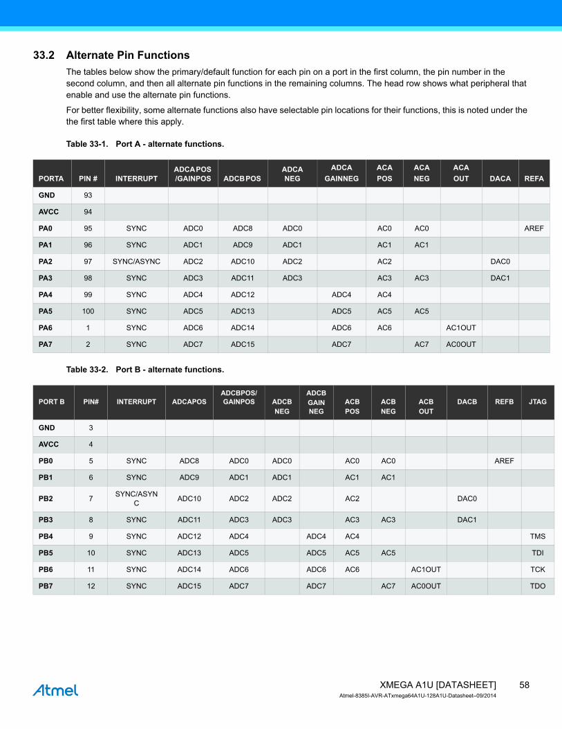
58XMEGA A1U [DATASHEET]Atmel-8385I-AVR-ATxmega64A1U-128A1U-Datasheet–09/2014
33.2 Alternate Pin FunctionsThe tables below show the primary/default function for each pin on a port in the first column, the pin number in the second column, and then all alternate pin functions in the remaining columns. The head row shows what peripheral that enable and use the alternate pin functions.
For better flexibility, some alternate functions also have selectable pin locations for their functions, this is noted under the the first table where this apply.
Table 33-1. Port A - alternate functions.
Table 33-2. Port B - alternate functions.
PORTA PIN # INTERRUPTADCA POS /GAINPOS ADCB POS
ADCA NEG
ADCAGAINNEG
ACAPOS
ACANEG
ACAOUT DACA REFA
GND 93
AVCC 94
PA0 95 SYNC ADC0 ADC8 ADC0 AC0 AC0 AREF
PA1 96 SYNC ADC1 ADC9 ADC1 AC1 AC1
PA2 97 SYNC/ASYNC ADC2 ADC10 ADC2 AC2 DAC0
PA3 98 SYNC ADC3 ADC11 ADC3 AC3 AC3 DAC1
PA4 99 SYNC ADC4 ADC12 ADC4 AC4
PA5 100 SYNC ADC5 ADC13 ADC5 AC5 AC5
PA6 1 SYNC ADC6 ADC14 ADC6 AC6 AC1OUT
PA7 2 SYNC ADC7 ADC15 ADC7 AC7 AC0OUT
PORT B PIN# INTERRUPT ADCAPOSADCBPOS/GAINPOS ADCB
NEG
ADCBGAIN NEG
ACBPOS
ACBNEG
ACBOUT
DACB REFB JTAG
GND 3
AVCC 4
PB0 5 SYNC ADC8 ADC0 ADC0 AC0 AC0 AREF
PB1 6 SYNC ADC9 ADC1 ADC1 AC1 AC1
PB2 7 SYNC/ASYNC ADC10 ADC2 ADC2 AC2 DAC0
PB3 8 SYNC ADC11 ADC3 ADC3 AC3 AC3 DAC1
PB4 9 SYNC ADC12 ADC4 ADC4 AC4 TMS
PB5 10 SYNC ADC13 ADC5 ADC5 AC5 AC5 TDI
PB6 11 SYNC ADC14 ADC6 ADC6 AC6 AC1OUT TCK
PB7 12 SYNC ADC15 ADC7 ADC7 AC7 AC0OUT TDO
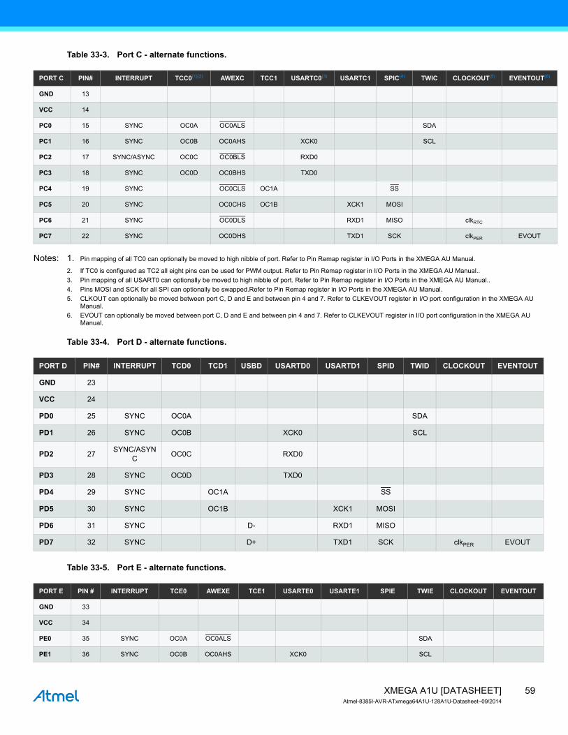
59XMEGA A1U [DATASHEET]Atmel-8385I-AVR-ATxmega64A1U-128A1U-Datasheet–09/2014
Table 33-3. Port C - alternate functions.
Notes: 1. Pin mapping of all TC0 can optionally be moved to high nibble of port. Refer to Pin Remap register in I/O Ports in the XMEGA AU Manual.
2. If TC0 is configured as TC2 all eight pins can be used for PWM output. Refer to Pin Remap register in I/O Ports in the XMEGA AU Manual..3. Pin mapping of all USART0 can optionally be moved to high nibble of port. Refer to Pin Remap register in I/O Ports in the XMEGA AU Manual..4. Pins MOSI and SCK for all SPI can optionally be swapped.Refer to Pin Remap register in I/O Ports in the XMEGA AU Manual.5. CLKOUT can optionally be moved between port C, D and E and between pin 4 and 7. Refer to CLKEVOUT register in I/O port configuration in the XMEGA AU
Manual. 6. EVOUT can optionally be moved between port C, D and E and between pin 4 and 7. Refer to CLKEVOUT register in I/O port configuration in the XMEGA AU
Manual.
Table 33-4. Port D - alternate functions.
Table 33-5. Port E - alternate functions.
PORT C PIN# INTERRUPT TCC0(1)(2) AWEXC TCC1 USARTC0(3) USARTC1 SPIC(4) TWIC CLOCKOUT(5) EVENTOUT(6)
GND 13
VCC 14
PC0 15 SYNC OC0A OC0ALS SDA
PC1 16 SYNC OC0B OC0AHS XCK0 SCL
PC2 17 SYNC/ASYNC OC0C OC0BLS RXD0
PC3 18 SYNC OC0D OC0BHS TXD0
PC4 19 SYNC OC0CLS OC1A SS
PC5 20 SYNC OC0CHS OC1B XCK1 MOSI
PC6 21 SYNC OC0DLS RXD1 MISO clkRTC
PC7 22 SYNC OC0DHS TXD1 SCK clkPER EVOUT
PORT D PIN# INTERRUPT TCD0 TCD1 USBD USARTD0 USARTD1 SPID TWID CLOCKOUT EVENTOUT
GND 23
VCC 24
PD0 25 SYNC OC0A SDA
PD1 26 SYNC OC0B XCK0 SCL
PD2 27 SYNC/ASYNC OC0C RXD0
PD3 28 SYNC OC0D TXD0
PD4 29 SYNC OC1A SS
PD5 30 SYNC OC1B XCK1 MOSI
PD6 31 SYNC D- RXD1 MISO
PD7 32 SYNC D+ TXD1 SCK clkPER EVOUT
PORT E PIN # INTERRUPT TCE0 AWEXE TCE1 USARTE0 USARTE1 SPIE TWIE CLOCKOUT EVENTOUT
GND 33
VCC 34
PE0 35 SYNC OC0A OC0ALS SDA
PE1 36 SYNC OC0B OC0AHS XCK0 SCL
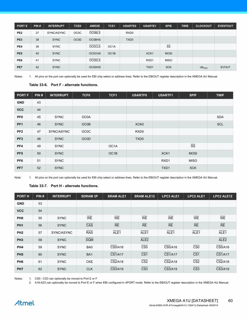
60XMEGA A1U [DATASHEET]Atmel-8385I-AVR-ATxmega64A1U-128A1U-Datasheet–09/2014
Notes: 1. All pins on the port can optionally be used for EBI chip select or address lines. Refer to the EBIOUT register description in the XMEGA AU Manual.
Table 33-6. Port F - alternate functions.
Note: 1. All pins on the port can optionally be used for EBI chip select or address lines. Refer to the EBIOUT register description in the XMEGA AU Manual.
Table 33-7. Port H - alternate functions.
Notes: 1. CS0 - CS3 can optionally be moved to Port E or F2. A16-A23 can optionally be moved to Port E or F when EBI configured in 4PORT mode. Refer to the EBIOUT register description in the XMEGA AU Manual.
PE2 37 SYNC/ASYNC OC0C OC0BLS RXD0
PE3 38 SYNC OC0D OC0BHS TXD0
PE4 39 SYNC OC0CLS OC1A SS
PE5 40 SYNC OC0CHS OC1B XCK1 MOSI
PE6 41 SYNC OC0DLS RXD1 MISO
PE7 42 SYNC OC0DHS TXD1 SCK clkPER EVOUT
PORT E PIN # INTERRUPT TCE0 AWEXE TCE1 USARTE0 USARTE1 SPIE TWIE CLOCKOUT EVENTOUT
PORT F PIN # INTERRUPT TCF0 TCF1 USARTF0 USARTF1 SPIF TWIF
GND 43
VCC 44
PF0 45 SYNC OC0A SDA
PF1 46 SYNC OC0B XCK0 SCL
PF2 47 SYNC/ASYNC OC0C RXD0
PF3 48 SYNC OC0D TXD0
PF4 49 SYNC OC1A SS
PF5 50 SYNC OC1B XCK1 MOSI
PF6 51 SYNC RXD1 MISO
PF7 52 SYNC TXD1 SCK
PORT H PIN # INTERRUPT SDRAM 3P SRAM ALE1 SRAM ALE12 LPC3 ALE1 LPC2 ALE1 LPC2 ALE12
GND 53
VCC 54
PH0 55 SYNC WE WE WE WE WE WE
PH1 56 SYNC CAS RE RE RE RE RE
PH2 57 SYNC/ASYNC RAS ALE1 ALE1 ALE1 ALE1 ALE1
PH3 58 SYNC DQM ALE2 ALE2
PH4 59 SYNC BA0 CS0/A16 CS0 CS0/A16 CS0 CS0/A16
PH5 60 SYNC BA1 CS1/A17 CS1 CS1/A17 CS1 CS1/A17
PH6 61 SYNC CKE CS2/A18 CS2 CS2/A18 CS2 CS2/A18
PH7 62 SYNC CLK CS3/A19 CS3 CS3/A19 CS3 CS3/A19
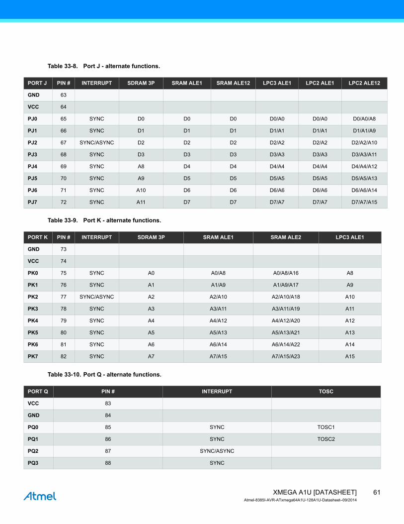
61XMEGA A1U [DATASHEET]Atmel-8385I-AVR-ATxmega64A1U-128A1U-Datasheet–09/2014
Table 33-8. Port J - alternate functions.
Table 33-9. Port K - alternate functions.
Table 33-10. Port Q - alternate functions.
PORT J PIN # INTERRUPT SDRAM 3P SRAM ALE1 SRAM ALE12 LPC3 ALE1 LPC2 ALE1 LPC2 ALE12
GND 63
VCC 64
PJ0 65 SYNC D0 D0 D0 D0/A0 D0/A0 D0/A0/A8
PJ1 66 SYNC D1 D1 D1 D1/A1 D1/A1 D1/A1/A9
PJ2 67 SYNC/ASYNC D2 D2 D2 D2/A2 D2/A2 D2/A2/A10
PJ3 68 SYNC D3 D3 D3 D3/A3 D3/A3 D3/A3/A11
PJ4 69 SYNC A8 D4 D4 D4/A4 D4/A4 D4/A4/A12
PJ5 70 SYNC A9 D5 D5 D5/A5 D5/A5 D5/A5/A13
PJ6 71 SYNC A10 D6 D6 D6/A6 D6/A6 D6/A6/A14
PJ7 72 SYNC A11 D7 D7 D7/A7 D7/A7 D7/A7/A15
PORT K PIN # INTERRUPT SDRAM 3P SRAM ALE1 SRAM ALE2 LPC3 ALE1
GND 73
VCC 74
PK0 75 SYNC A0 A0/A8 A0/A8/A16 A8
PK1 76 SYNC A1 A1/A9 A1/A9/A17 A9
PK2 77 SYNC/ASYNC A2 A2/A10 A2/A10/A18 A10
PK3 78 SYNC A3 A3/A11 A3/A11/A19 A11
PK4 79 SYNC A4 A4/A12 A4/A12/A20 A12
PK5 80 SYNC A5 A5/A13 A5/A13/A21 A13
PK6 81 SYNC A6 A6/A14 A6/A14/A22 A14
PK7 82 SYNC A7 A7/A15 A7/A15/A23 A15
PORT Q PIN # INTERRUPT TOSC
VCC 83
GND 84
PQ0 85 SYNC TOSC1
PQ1 86 SYNC TOSC2
PQ2 87 SYNC/ASYNC
PQ3 88 SYNC
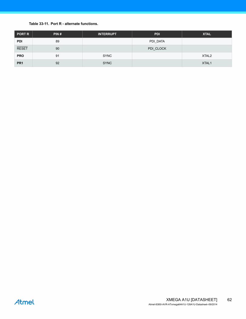
62XMEGA A1U [DATASHEET]Atmel-8385I-AVR-ATxmega64A1U-128A1U-Datasheet–09/2014
Table 33-11. Port R - alternate functions.
PORT R PIN # INTERRUPT PDI XTAL
PDI 89 PDI_DATA
RESET 90 PDI_CLOCK
PRO 91 SYNC XTAL2
PR1 92 SYNC XTAL1
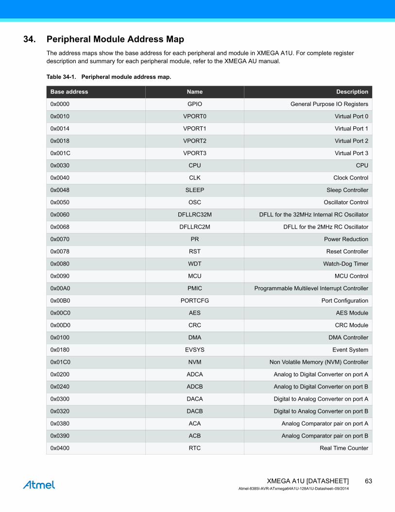
63XMEGA A1U [DATASHEET]Atmel-8385I-AVR-ATxmega64A1U-128A1U-Datasheet–09/2014
34. Peripheral Module Address MapThe address maps show the base address for each peripheral and module in XMEGA A1U. For complete register description and summary for each peripheral module, refer to the XMEGA AU manual.
Table 34-1. Peripheral module address map.
Base address Name Description
0x0000 GPIO General Purpose IO Registers
0x0010 VPORT0 Virtual Port 0
0x0014 VPORT1 Virtual Port 1
0x0018 VPORT2 Virtual Port 2
0x001C VPORT3 Virtual Port 3
0x0030 CPU CPU
0x0040 CLK Clock Control
0x0048 SLEEP Sleep Controller
0x0050 OSC Oscillator Control
0x0060 DFLLRC32M DFLL for the 32MHz Internal RC Oscillator
0x0068 DFLLRC2M DFLL for the 2MHz RC Oscillator
0x0070 PR Power Reduction
0x0078 RST Reset Controller
0x0080 WDT Watch-Dog Timer
0x0090 MCU MCU Control
0x00A0 PMIC Programmable Multilevel Interrupt Controller
0x00B0 PORTCFG Port Configuration
0x00C0 AES AES Module
0x00D0 CRC CRC Module
0x0100 DMA DMA Controller
0x0180 EVSYS Event System
0x01C0 NVM Non Volatile Memory (NVM) Controller
0x0200 ADCA Analog to Digital Converter on port A
0x0240 ADCB Analog to Digital Converter on port B
0x0300 DACA Digital to Analog Converter on port A
0x0320 DACB Digital to Analog Converter on port B
0x0380 ACA Analog Comparator pair on port A
0x0390 ACB Analog Comparator pair on port B
0x0400 RTC Real Time Counter
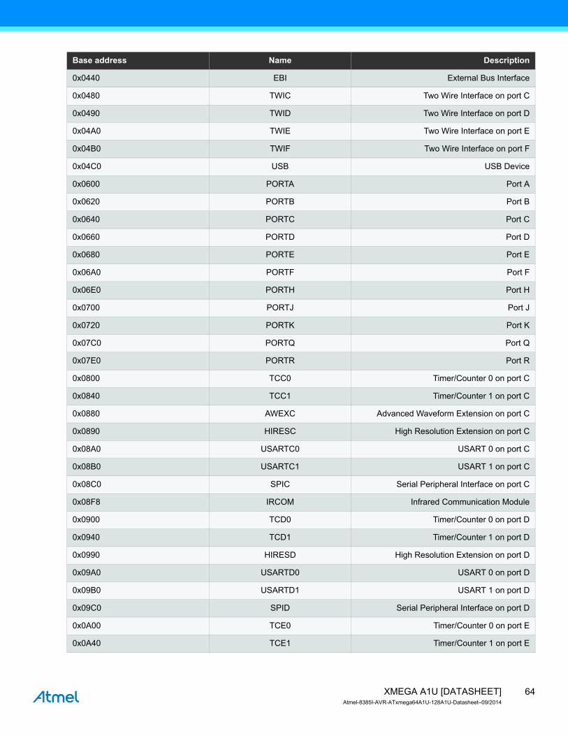
64XMEGA A1U [DATASHEET]Atmel-8385I-AVR-ATxmega64A1U-128A1U-Datasheet–09/2014
0x0440 EBI External Bus Interface
0x0480 TWIC Two Wire Interface on port C
0x0490 TWID Two Wire Interface on port D
0x04A0 TWIE Two Wire Interface on port E
0x04B0 TWIF Two Wire Interface on port F
0x04C0 USB USB Device
0x0600 PORTA Port A
0x0620 PORTB Port B
0x0640 PORTC Port C
0x0660 PORTD Port D
0x0680 PORTE Port E
0x06A0 PORTF Port F
0x06E0 PORTH Port H
0x0700 PORTJ Port J
0x0720 PORTK Port K
0x07C0 PORTQ Port Q
0x07E0 PORTR Port R
0x0800 TCC0 Timer/Counter 0 on port C
0x0840 TCC1 Timer/Counter 1 on port C
0x0880 AWEXC Advanced Waveform Extension on port C
0x0890 HIRESC High Resolution Extension on port C
0x08A0 USARTC0 USART 0 on port C
0x08B0 USARTC1 USART 1 on port C
0x08C0 SPIC Serial Peripheral Interface on port C
0x08F8 IRCOM Infrared Communication Module
0x0900 TCD0 Timer/Counter 0 on port D
0x0940 TCD1 Timer/Counter 1 on port D
0x0990 HIRESD High Resolution Extension on port D
0x09A0 USARTD0 USART 0 on port D
0x09B0 USARTD1 USART 1 on port D
0x09C0 SPID Serial Peripheral Interface on port D
0x0A00 TCE0 Timer/Counter 0 on port E
0x0A40 TCE1 Timer/Counter 1 on port E
Base address Name Description
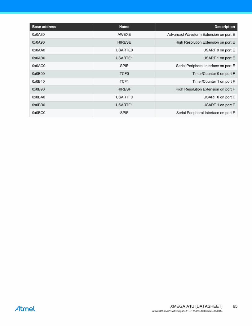
65XMEGA A1U [DATASHEET]Atmel-8385I-AVR-ATxmega64A1U-128A1U-Datasheet–09/2014
0x0A80 AWEXE Advanced Waveform Extension on port E
0x0A90 HIRESE High Resolution Extension on port E
0x0AA0 USARTE0 USART 0 on port E
0x0AB0 USARTE1 USART 1 on port E
0x0AC0 SPIE Serial Peripheral Interface on port E
0x0B00 TCF0 Timer/Counter 0 on port F
0x0B40 TCF1 Timer/Counter 1 on port F
0x0B90 HIRESF High Resolution Extension on port F
0x0BA0 USARTF0 USART 0 on port F
0x0BB0 USARTF1 USART 1 on port F
0x0BC0 SPIF Serial Peripheral Interface on port F
Base address Name Description
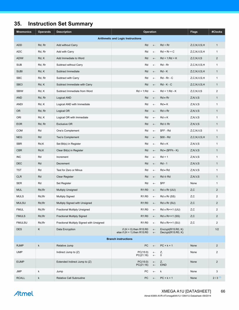
66XMEGA A1U [DATASHEET]Atmel-8385I-AVR-ATxmega64A1U-128A1U-Datasheet–09/2014
35. Instruction Set SummaryMnemonics Operands Description Operation Flags #Clocks
Arithmetic and Logic Instructions
ADD Rd, Rr Add without Carry Rd ← Rd + Rr Z,C,N,V,S,H 1
ADC Rd, Rr Add with Carry Rd ← Rd + Rr + C Z,C,N,V,S,H 1
ADIW Rd, K Add Immediate to Word Rd ← Rd + 1:Rd + K Z,C,N,V,S 2
SUB Rd, Rr Subtract without Carry Rd ← Rd - Rr Z,C,N,V,S,H 1
SUBI Rd, K Subtract Immediate Rd ← Rd - K Z,C,N,V,S,H 1
SBC Rd, Rr Subtract with Carry Rd ← Rd - Rr - C Z,C,N,V,S,H 1
SBCI Rd, K Subtract Immediate with Carry Rd ← Rd - K - C Z,C,N,V,S,H 1
SBIW Rd, K Subtract Immediate from Word Rd + 1:Rd ← Rd + 1:Rd - K Z,C,N,V,S 2
AND Rd, Rr Logical AND Rd ← Rd • Rr Z,N,V,S 1
ANDI Rd, K Logical AND with Immediate Rd ← Rd • K Z,N,V,S 1
OR Rd, Rr Logical OR Rd ← Rd v Rr Z,N,V,S 1
ORI Rd, K Logical OR with Immediate Rd ← Rd v K Z,N,V,S 1
EOR Rd, Rr Exclusive OR Rd ← Rd ⊕ Rr Z,N,V,S 1
COM Rd One’s Complement Rd ← $FF - Rd Z,C,N,V,S 1
NEG Rd Two’s Complement Rd ← $00 - Rd Z,C,N,V,S,H 1
SBR Rd,K Set Bit(s) in Register Rd ← Rd v K Z,N,V,S 1
CBR Rd,K Clear Bit(s) in Register Rd ← Rd • ($FFh - K) Z,N,V,S 1
INC Rd Increment Rd ← Rd + 1 Z,N,V,S 1
DEC Rd Decrement Rd ← Rd - 1 Z,N,V,S 1
TST Rd Test for Zero or Minus Rd ← Rd • Rd Z,N,V,S 1
CLR Rd Clear Register Rd ← Rd ⊕ Rd Z,N,V,S 1
SER Rd Set Register Rd ← $FF None 1
MUL Rd,Rr Multiply Unsigned R1:R0 ← Rd x Rr (UU) Z,C 2
MULS Rd,Rr Multiply Signed R1:R0 ← Rd x Rr (SS) Z,C 2
MULSU Rd,Rr Multiply Signed with Unsigned R1:R0 ← Rd x Rr (SU) Z,C 2
FMUL Rd,Rr Fractional Multiply Unsigned R1:R0 ← Rd x Rr<<1 (UU) Z,C 2
FMULS Rd,Rr Fractional Multiply Signed R1:R0 ← Rd x Rr<<1 (SS) Z,C 2
FMULSU Rd,Rr Fractional Multiply Signed with Unsigned R1:R0 ← Rd x Rr<<1 (SU) Z,C 2
DES K Data Encryption if (H = 0) then R15:R0else if (H = 1) then R15:R0
←←
Encrypt(R15:R0, K)Decrypt(R15:R0, K)
1/2
Branch instructions
RJMP k Relative Jump PC ← PC + k + 1 None 2
IJMP Indirect Jump to (Z) PC(15:0)PC(21:16)
←←
Z,0
None 2
EIJMP Extended Indirect Jump to (Z) PC(15:0)PC(21:16)
←←
Z,EIND
None 2
JMP k Jump PC ← k None 3
RCALL k Relative Call Subroutine PC ← PC + k + 1 None 2 / 3 (1)
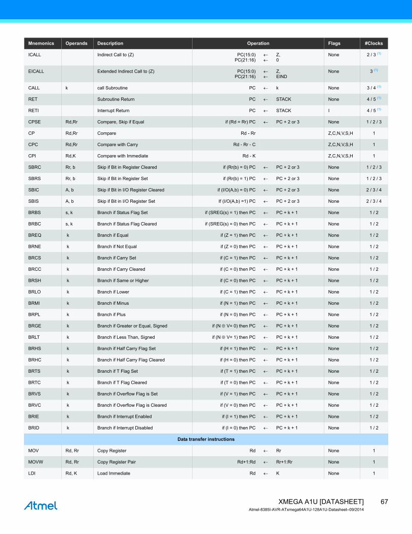
67XMEGA A1U [DATASHEET]Atmel-8385I-AVR-ATxmega64A1U-128A1U-Datasheet–09/2014
ICALL Indirect Call to (Z) PC(15:0)PC(21:16)
←←
Z,0
None 2 / 3 (1)
EICALL Extended Indirect Call to (Z) PC(15:0)PC(21:16)
←←
Z,EIND
None 3 (1)
CALL k call Subroutine PC ← k None 3 / 4 (1)
RET Subroutine Return PC ← STACK None 4 / 5 (1)
RETI Interrupt Return PC ← STACK I 4 / 5 (1)
CPSE Rd,Rr Compare, Skip if Equal if (Rd = Rr) PC ← PC + 2 or 3 None 1 / 2 / 3
CP Rd,Rr Compare Rd - Rr Z,C,N,V,S,H 1
CPC Rd,Rr Compare with Carry Rd - Rr - C Z,C,N,V,S,H 1
CPI Rd,K Compare with Immediate Rd - K Z,C,N,V,S,H 1
SBRC Rr, b Skip if Bit in Register Cleared if (Rr(b) = 0) PC ← PC + 2 or 3 None 1 / 2 / 3
SBRS Rr, b Skip if Bit in Register Set if (Rr(b) = 1) PC ← PC + 2 or 3 None 1 / 2 / 3
SBIC A, b Skip if Bit in I/O Register Cleared if (I/O(A,b) = 0) PC ← PC + 2 or 3 None 2 / 3 / 4
SBIS A, b Skip if Bit in I/O Register Set If (I/O(A,b) =1) PC ← PC + 2 or 3 None 2 / 3 / 4
BRBS s, k Branch if Status Flag Set if (SREG(s) = 1) then PC ← PC + k + 1 None 1 / 2
BRBC s, k Branch if Status Flag Cleared if (SREG(s) = 0) then PC ← PC + k + 1 None 1 / 2
BREQ k Branch if Equal if (Z = 1) then PC ← PC + k + 1 None 1 / 2
BRNE k Branch if Not Equal if (Z = 0) then PC ← PC + k + 1 None 1 / 2
BRCS k Branch if Carry Set if (C = 1) then PC ← PC + k + 1 None 1 / 2
BRCC k Branch if Carry Cleared if (C = 0) then PC ← PC + k + 1 None 1 / 2
BRSH k Branch if Same or Higher if (C = 0) then PC ← PC + k + 1 None 1 / 2
BRLO k Branch if Lower if (C = 1) then PC ← PC + k + 1 None 1 / 2
BRMI k Branch if Minus if (N = 1) then PC ← PC + k + 1 None 1 / 2
BRPL k Branch if Plus if (N = 0) then PC ← PC + k + 1 None 1 / 2
BRGE k Branch if Greater or Equal, Signed if (N ⊕ V= 0) then PC ← PC + k + 1 None 1 / 2
BRLT k Branch if Less Than, Signed if (N ⊕ V= 1) then PC ← PC + k + 1 None 1 / 2
BRHS k Branch if Half Carry Flag Set if (H = 1) then PC ← PC + k + 1 None 1 / 2
BRHC k Branch if Half Carry Flag Cleared if (H = 0) then PC ← PC + k + 1 None 1 / 2
BRTS k Branch if T Flag Set if (T = 1) then PC ← PC + k + 1 None 1 / 2
BRTC k Branch if T Flag Cleared if (T = 0) then PC ← PC + k + 1 None 1 / 2
BRVS k Branch if Overflow Flag is Set if (V = 1) then PC ← PC + k + 1 None 1 / 2
BRVC k Branch if Overflow Flag is Cleared if (V = 0) then PC ← PC + k + 1 None 1 / 2
BRIE k Branch if Interrupt Enabled if (I = 1) then PC ← PC + k + 1 None 1 / 2
BRID k Branch if Interrupt Disabled if (I = 0) then PC ← PC + k + 1 None 1 / 2
Data transfer instructions
MOV Rd, Rr Copy Register Rd ← Rr None 1
MOVW Rd, Rr Copy Register Pair Rd+1:Rd ← Rr+1:Rr None 1
LDI Rd, K Load Immediate Rd ← K None 1
Mnemonics Operands Description Operation Flags #Clocks
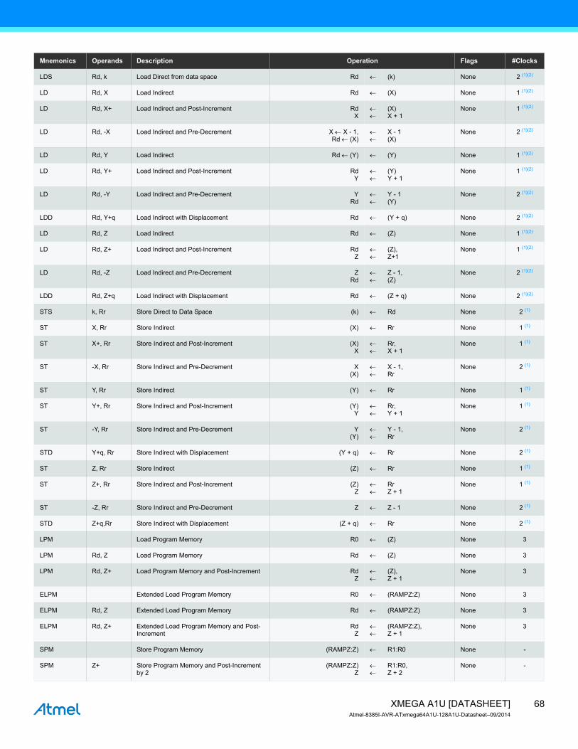
68XMEGA A1U [DATASHEET]Atmel-8385I-AVR-ATxmega64A1U-128A1U-Datasheet–09/2014
LDS Rd, k Load Direct from data space Rd ← (k) None 2 (1)(2)
LD Rd, X Load Indirect Rd ← (X) None 1 (1)(2)
LD Rd, X+ Load Indirect and Post-Increment RdX
←←
(X)X + 1
None 1 (1)(2)
LD Rd, -X Load Indirect and Pre-Decrement X ← X - 1,Rd ← (X)
←←
X - 1(X)
None 2 (1)(2)
LD Rd, Y Load Indirect Rd ← (Y) ← (Y) None 1 (1)(2)
LD Rd, Y+ Load Indirect and Post-Increment RdY
←←
(Y)Y + 1
None 1 (1)(2)
LD Rd, -Y Load Indirect and Pre-Decrement YRd
←←
Y - 1(Y)
None 2 (1)(2)
LDD Rd, Y+q Load Indirect with Displacement Rd ← (Y + q) None 2 (1)(2)
LD Rd, Z Load Indirect Rd ← (Z) None 1 (1)(2)
LD Rd, Z+ Load Indirect and Post-Increment RdZ
←←
(Z),Z+1
None 1 (1)(2)
LD Rd, -Z Load Indirect and Pre-Decrement ZRd
←←
Z - 1,(Z)
None 2 (1)(2)
LDD Rd, Z+q Load Indirect with Displacement Rd ← (Z + q) None 2 (1)(2)
STS k, Rr Store Direct to Data Space (k) ← Rd None 2 (1)
ST X, Rr Store Indirect (X) ← Rr None 1 (1)
ST X+, Rr Store Indirect and Post-Increment (X)X
←←
Rr,X + 1
None 1 (1)
ST -X, Rr Store Indirect and Pre-Decrement X(X)
←←
X - 1,Rr
None 2 (1)
ST Y, Rr Store Indirect (Y) ← Rr None 1 (1)
ST Y+, Rr Store Indirect and Post-Increment (Y)Y
←←
Rr,Y + 1
None 1 (1)
ST -Y, Rr Store Indirect and Pre-Decrement Y(Y)
←←
Y - 1,Rr
None 2 (1)
STD Y+q, Rr Store Indirect with Displacement (Y + q) ← Rr None 2 (1)
ST Z, Rr Store Indirect (Z) ← Rr None 1 (1)
ST Z+, Rr Store Indirect and Post-Increment (Z)Z
←←
RrZ + 1
None 1 (1)
ST -Z, Rr Store Indirect and Pre-Decrement Z ← Z - 1 None 2 (1)
STD Z+q,Rr Store Indirect with Displacement (Z + q) ← Rr None 2 (1)
LPM Load Program Memory R0 ← (Z) None 3
LPM Rd, Z Load Program Memory Rd ← (Z) None 3
LPM Rd, Z+ Load Program Memory and Post-Increment RdZ
←←
(Z),Z + 1
None 3
ELPM Extended Load Program Memory R0 ← (RAMPZ:Z) None 3
ELPM Rd, Z Extended Load Program Memory Rd ← (RAMPZ:Z) None 3
ELPM Rd, Z+ Extended Load Program Memory and Post-Increment
RdZ
←←
(RAMPZ:Z),Z + 1
None 3
SPM Store Program Memory (RAMPZ:Z) ← R1:R0 None -
SPM Z+ Store Program Memory and Post-Increment by 2
(RAMPZ:Z)Z
←←
R1:R0,Z + 2
None -
Mnemonics Operands Description Operation Flags #Clocks
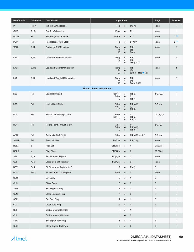
69XMEGA A1U [DATASHEET]Atmel-8385I-AVR-ATxmega64A1U-128A1U-Datasheet–09/2014
IN Rd, A In From I/O Location Rd ← I/O(A) None 1
OUT A, Rr Out To I/O Location I/O(A) ← Rr None 1
PUSH Rr Push Register on Stack STACK ← Rr None 1 (1)
POP Rd Pop Register from Stack Rd ← STACK None 2 (1)
XCH Z, Rd Exchange RAM location TempRd(Z)
←←←
Rd,(Z),Temp
None 2
LAS Z, Rd Load and Set RAM location TempRd(Z)
←←←
Rd,(Z),Temp v (Z)
None 2
LAC Z, Rd Load and Clear RAM location TempRd(Z)
←←←
Rd,(Z),($FFh – Rd) z (Z)
None 2
LAT Z, Rd Load and Toggle RAM location TempRd(Z)
←←←
Rd,(Z),Temp ⊕ (Z)
None 2
Bit and bit-test instructions
LSL Rd Logical Shift Left Rd(n+1)Rd(0)
C
←←←
Rd(n),0,Rd(7)
Z,C,N,V,H 1
LSR Rd Logical Shift Right Rd(n)Rd(7)
C
←←←
Rd(n+1),0,Rd(0)
Z,C,N,V 1
ROL Rd Rotate Left Through Carry Rd(0)Rd(n+1)
C
←←←
C,Rd(n),Rd(7)
Z,C,N,V,H 1
ROR Rd Rotate Right Through Carry Rd(7)Rd(n)
C
←←←
C,Rd(n+1),Rd(0)
Z,C,N,V 1
ASR Rd Arithmetic Shift Right Rd(n) ← Rd(n+1), n=0..6 Z,C,N,V 1
SWAP Rd Swap Nibbles Rd(3..0) ↔ Rd(7..4) None 1
BSET s Flag Set SREG(s) ← 1 SREG(s) 1
BCLR s Flag Clear SREG(s) ← 0 SREG(s) 1
SBI A, b Set Bit in I/O Register I/O(A, b) ← 1 None 1
CBI A, b Clear Bit in I/O Register I/O(A, b) ← 0 None 1
BST Rr, b Bit Store from Register to T T ← Rr(b) T 1
BLD Rd, b Bit load from T to Register Rd(b) ← T None 1
SEC Set Carry C ← 1 C 1
CLC Clear Carry C ← 0 C 1
SEN Set Negative Flag N ← 1 N 1
CLN Clear Negative Flag N ← 0 N 1
SEZ Set Zero Flag Z ← 1 Z 1
CLZ Clear Zero Flag Z ← 0 Z 1
SEI Global Interrupt Enable I ← 1 I 1
CLI Global Interrupt Disable I ← 0 I 1
SES Set Signed Test Flag S ← 1 S 1
CLS Clear Signed Test Flag S ← 0 S 1
Mnemonics Operands Description Operation Flags #Clocks
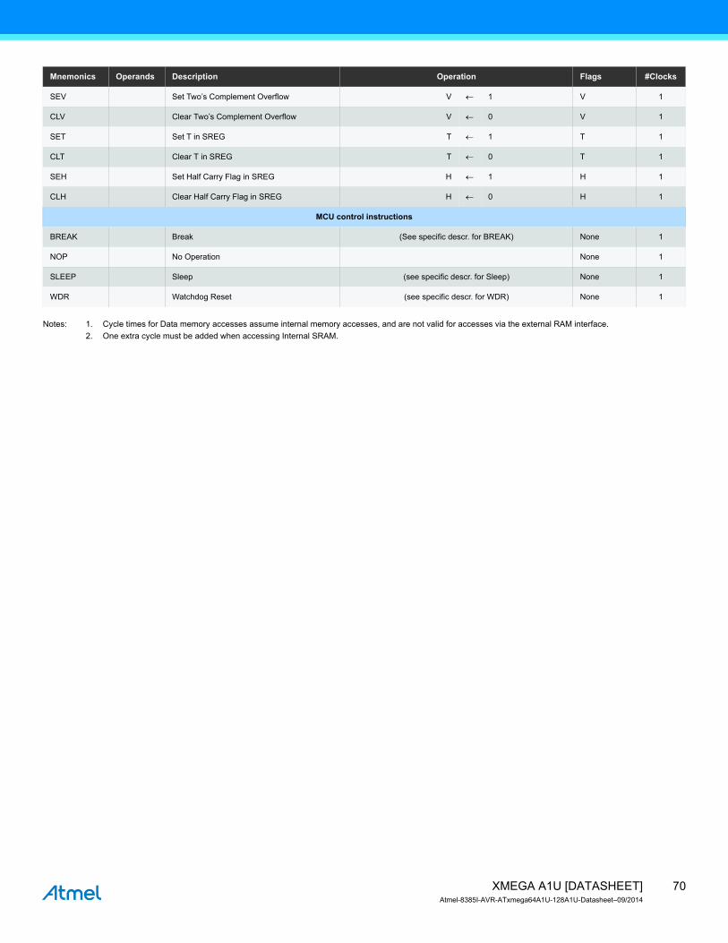
70XMEGA A1U [DATASHEET]Atmel-8385I-AVR-ATxmega64A1U-128A1U-Datasheet–09/2014
Notes: 1. Cycle times for Data memory accesses assume internal memory accesses, and are not valid for accesses via the external RAM interface.2. One extra cycle must be added when accessing Internal SRAM.
SEV Set Two’s Complement Overflow V ← 1 V 1
CLV Clear Two’s Complement Overflow V ← 0 V 1
SET Set T in SREG T ← 1 T 1
CLT Clear T in SREG T ← 0 T 1
SEH Set Half Carry Flag in SREG H ← 1 H 1
CLH Clear Half Carry Flag in SREG H ← 0 H 1
MCU control instructions
BREAK Break (See specific descr. for BREAK) None 1
NOP No Operation None 1
SLEEP Sleep (see specific descr. for Sleep) None 1
WDR Watchdog Reset (see specific descr. for WDR) None 1
Mnemonics Operands Description Operation Flags #Clocks
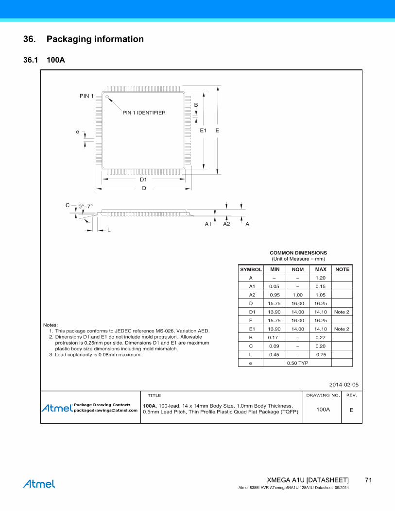
71XMEGA A1U [DATASHEET]Atmel-8385I-AVR-ATxmega64A1U-128A1U-Datasheet–09/2014
36. Packaging information
36.1 100A
100A, 100-lead, 14 x 14mm Body Size, 1.0mm Body Thickness, 0.5mm Lead Pitch, Thin Profile Plastic Quad Flat Package (TQFP) 100A E
2014-02-05
PIN 1 IDENTIFIER
0°~7°
PIN 1
L
C
A1 A2 A
D1
D
e E1 E
B
A – – 1.20
A1 0.05 – 0.15
A2 0.95 1.00 1.05
D 15.75 16.00 16.25
D1 13.90 14.00 14.10 Note 2
E 15.75 16.00 16.25
E1 13.90 14.00 14.10 Note 2
B 0.17 – 0.27
C 0.09 – 0.20
L 0.45 – 0.75
e 0.50 TYP
Notes: 1. This package conforms to JEDEC reference MS-026, Variation AED. 2. Dimensions D1 and E1 do not include mold protrusion. Allowable protrusion is 0.25mm per side. Dimensions D1 and E1 are maximum plastic body size dimensions including mold mismatch. 3. Lead coplanarity is 0.08mm maximum.
COMMON DIMENSIONS(Unit of Measure = mm)
SYMBOL MIN NOM MAX NOTE
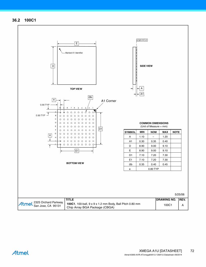
72XMEGA A1U [DATASHEET]Atmel-8385I-AVR-ATxmega64A1U-128A1U-Datasheet–09/2014
36.2 100C1
2325 Orchard Parkway San Jose, CA 95131
TITLE DRAWING NO. REV. 100C1, 100-ball, 9 x 9 x 1.2 mm Body, Ball Pitch 0.80 mm Chip Array BGA Package (CBGA)
A100C1
5/25/06
TOP VIEW
SIDE VIEW
BOTTOM VIEW
COMMON DIMENSIONS(Unit of Measure = mm)
SYMBOL MIN NOM MAX NOTE
A 1.10 – 1.20
A1 0.30 0.35 0.40
D 8.90 9.00 9.10
E 8.90 9.00 9.10
D1 7.10 7.20 7.30
E1 7.10 7.20 7.30
Øb 0.35 0.40 0.45
e 0.80 TYP
Marked A1 Identifier
12345678
A
B
C
D
E
9
F
G
H
I
J
10
0.90 TYP
0.90 TYP
A1 Corner
0.12 Z
E
D
e
e
Øb
A
A1
E1
D1
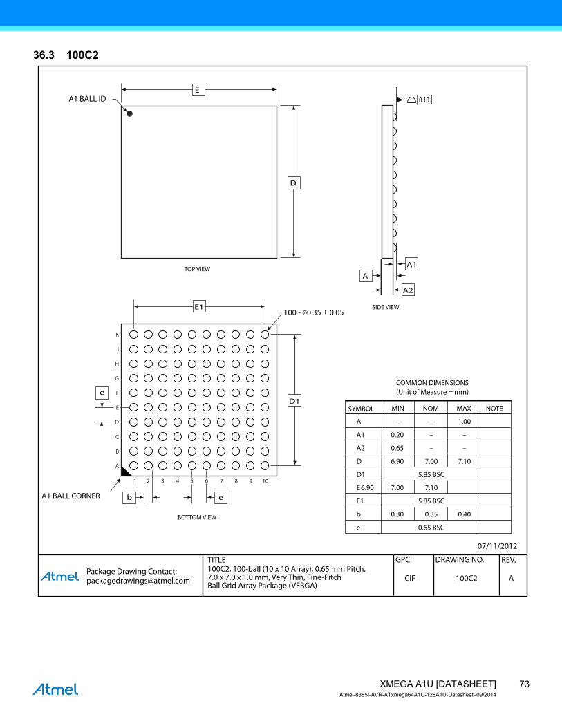
73XMEGA A1U [DATASHEET]Atmel-8385I-AVR-ATxmega64A1U-128A1U-Datasheet–09/2014
36.3 100C2
TITLE DRAWING NO.GPC REV. Package Drawing Contact: [email protected] 100C2CIF A
100C2, 100-ball (10 x 10 Array), 0.65 mm Pitch, 7.0 x 7.0 x 1.0 mm, Very Thin, Fine-Pitch Ball Grid Array Package (VFBGA)
07/11/2012
COMMON DIMENSIONS(Unit of Measure = mm)
SYMBOL MIN NOM MAX NOTE
A – – 1.00
A1 0.20 – –
A2 0.65 – –
D 6.90 7.00 7.10
D1 5.85 BSC
E 6.90 7.00 7.10
E1 5.85 BSC
b 0.30 0.35 0.40
e 0.65 BSC
TOP VIEW
SIDE VIEW
A1 BALL ID
K
J
H
G
F
E
D
C
B
A
1 2 3 4 5 6 7 8 9 10
AA1
A2
D
E0.10
E1
D1
100 - Ø0.35 ± 0.05
e
A1 BALL CORNER
BOTTOM VIEW
b e
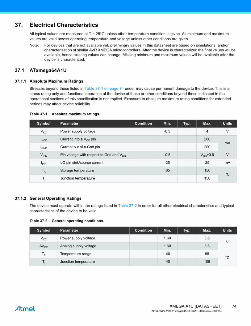
74XMEGA A1U [DATASHEET]Atmel-8385I-AVR-ATxmega64A1U-128A1U-Datasheet–09/2014
37. Electrical CharacteristicsAll typical values are measured at T = 25°C unless other temperature condition is given. All minimum and maximum values are valid across operating temperature and voltage unless other conditions are given.Note: For devices that are not available yet, preliminary values in this datasheet are based on simulations, and/or
characterization of similar AVR XMEGA microcontrollers. After the device is characterized the final values will be available, hence existing values can change. Missing minimum and maximum values will be available after the device is characterized.
37.1 ATxmega64A1U
37.1.1 Absolute Maximum Ratings
Stresses beyond those listed in Table 37-1 on page 74 under may cause permanent damage to the device. This is a stress rating only and functional operation of the device at these or other conditions beyond those indicated in the operational sections of this specification is not implied. Exposure to absolute maximum rating conditions for extended periods may affect device reliability.
Table 37-1. Absolute maximum ratings.
37.1.2 General Operating Ratings
The device must operate within the ratings listed in Table 37-2 in order for all other electrical characteristics and typical characteristics of the device to be valid.
Table 37-2. General operating conditions.
Symbol Parameter Condition Min. Typ. Max. Units
VCC Power supply voltage -0.3 4 V
IVCC Current into a VCC pin 200mA
IGND Current out of a Gnd pin 200
VPIN Pin voltage with respect to Gnd and VCC -0.5 VCC+0.5 V
IPIN I/O pin sink/source current -25 25 mA
TA Storage temperature -65 150°C
Tj Junction temperature 150
Symbol Parameter Condition Min. Typ. Max. Units
VCC Power supply voltage 1.60 3.6V
AVCC Analog supply voltage 1.60 3.6
TA Temperature range -40 85°C
Tj Junction temperature -40 105
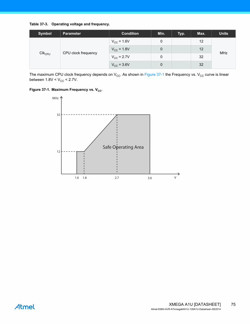
75XMEGA A1U [DATASHEET]Atmel-8385I-AVR-ATxmega64A1U-128A1U-Datasheet–09/2014
Table 37-3. Operating voltage and frequency.
The maximum CPU clock frequency depends on VCC. As shown in Figure 37-1 the Frequency vs. VCC curve is linear between 1.8V < VCC < 2.7V.
Figure 37-1. Maximum Frequency vs. VCC.
Symbol Parameter Condition Min. Typ. Max. Units
ClkCPU CPU clock frequency
VCC = 1.6V 0 12
MHzVCC = 1.8V 0 12
VCC = 2.7V 0 32
VCC = 3.6V 0 32
1.8
12
32
MHz
V2.7 3.61.6
Safe Operating Area
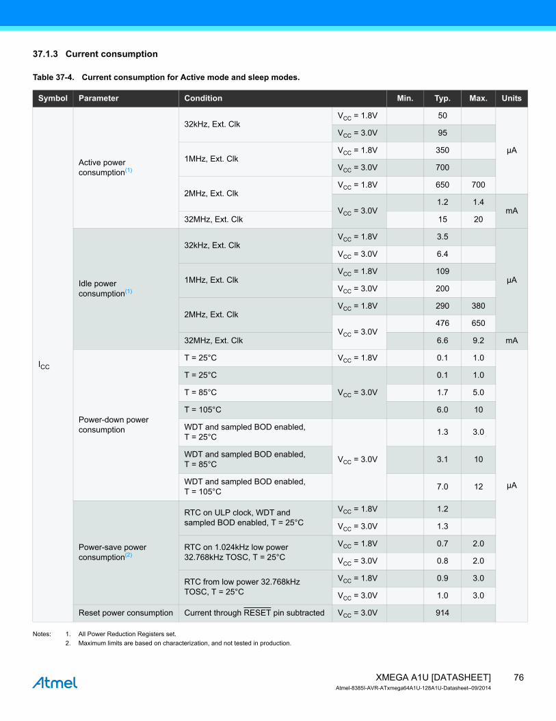
76XMEGA A1U [DATASHEET]Atmel-8385I-AVR-ATxmega64A1U-128A1U-Datasheet–09/2014
37.1.3 Current consumption
Table 37-4. Current consumption for Active mode and sleep modes.
Notes: 1. All Power Reduction Registers set.2. Maximum limits are based on characterization, and not tested in production.
Symbol Parameter Condition Min. Typ. Max. Units
ICC
Active power consumption(1)
32kHz, Ext. ClkVCC = 1.8V 50
µA
VCC = 3.0V 95
1MHz, Ext. ClkVCC = 1.8V 350
VCC = 3.0V 700
2MHz, Ext. ClkVCC = 1.8V 650 700
VCC = 3.0V1.2 1.4
mA32MHz, Ext. Clk 15 20
Idle powerconsumption(1)
32kHz, Ext. ClkVCC = 1.8V 3.5
µA
VCC = 3.0V 6.4
1MHz, Ext. ClkVCC = 1.8V 109
VCC = 3.0V 200
2MHz, Ext. ClkVCC = 1.8V 290 380
VCC = 3.0V476 650
32MHz, Ext. Clk 6.6 9.2 mA
Power-down power consumption
T = 25°C VCC = 1.8V 0.1 1.0
µA
T = 25°C
VCC = 3.0V
0.1 1.0
T = 85°C 1.7 5.0
T = 105°C 6.0 10
WDT and sampled BOD enabled,T = 25°C
VCC = 3.0V
1.3 3.0
WDT and sampled BOD enabled,T = 85°C 3.1 10
WDT and sampled BOD enabled,T = 105°C 7.0 12
Power-save power consumption(2)
RTC on ULP clock, WDT andsampled BOD enabled, T = 25°C
VCC = 1.8V 1.2
VCC = 3.0V 1.3
RTC on 1.024kHz low power32.768kHz TOSC, T = 25°C
VCC = 1.8V 0.7 2.0
VCC = 3.0V 0.8 2.0
RTC from low power 32.768kHzTOSC, T = 25°C
VCC = 1.8V 0.9 3.0
VCC = 3.0V 1.0 3.0
Reset power consumption Current through RESET pin subtracted VCC = 3.0V 914
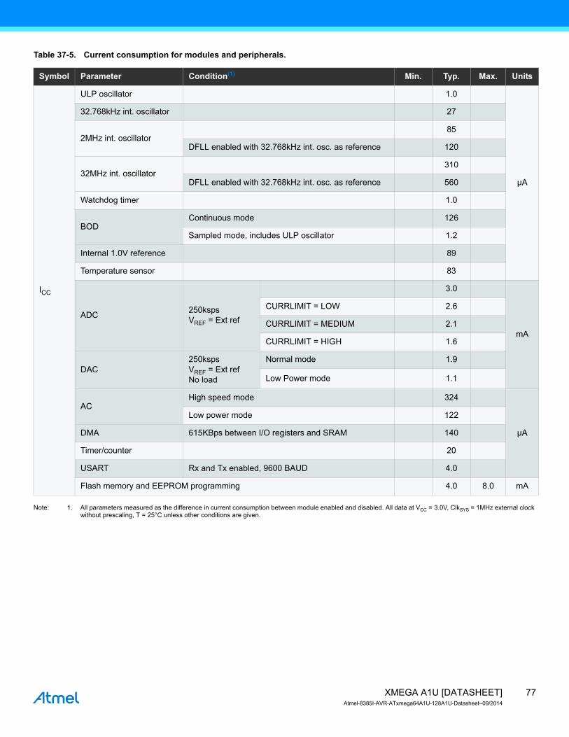
77XMEGA A1U [DATASHEET]Atmel-8385I-AVR-ATxmega64A1U-128A1U-Datasheet–09/2014
Table 37-5. Current consumption for modules and peripherals.
Note: 1. All parameters measured as the difference in current consumption between module enabled and disabled. All data at VCC = 3.0V, ClkSYS = 1MHz external clock without prescaling, T = 25°C unless other conditions are given.
Symbol Parameter Condition(1) Min. Typ. Max. Units
ICC
ULP oscillator 1.0
µA
32.768kHz int. oscillator 27
2MHz int. oscillator85
DFLL enabled with 32.768kHz int. osc. as reference 120
32MHz int. oscillator310
DFLL enabled with 32.768kHz int. osc. as reference 560
Watchdog timer 1.0
BODContinuous mode 126
Sampled mode, includes ULP oscillator 1.2
Internal 1.0V reference 89
Temperature sensor 83
ADC 250kspsVREF = Ext ref
3.0
mA
CURRLIMIT = LOW 2.6
CURRLIMIT = MEDIUM 2.1
CURRLIMIT = HIGH 1.6
DAC250kspsVREF = Ext refNo load
Normal mode 1.9
Low Power mode 1.1
ACHigh speed mode 324
µA
Low power mode 122
DMA 615KBps between I/O registers and SRAM 140
Timer/counter 20
USART Rx and Tx enabled, 9600 BAUD 4.0
Flash memory and EEPROM programming 4.0 8.0 mA
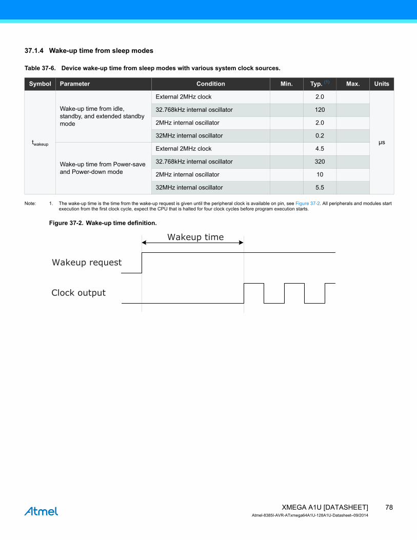
78XMEGA A1U [DATASHEET]Atmel-8385I-AVR-ATxmega64A1U-128A1U-Datasheet–09/2014
37.1.4 Wake-up time from sleep modes
Table 37-6. Device wake-up time from sleep modes with various system clock sources.
Note: 1. The wake-up time is the time from the wake-up request is given until the peripheral clock is available on pin, see Figure 37-2. All peripherals and modules start execution from the first clock cycle, expect the CPU that is halted for four clock cycles before program execution starts.
Figure 37-2. Wake-up time definition.
Symbol Parameter Condition Min. Typ. (1) Max. Units
twakeup
Wake-up time from idle, standby, and extended standby mode
External 2MHz clock 2.0
µs
32.768kHz internal oscillator 120
2MHz internal oscillator 2.0
32MHz internal oscillator 0.2
Wake-up time from Power-save and Power-down mode
External 2MHz clock 4.5
32.768kHz internal oscillator 320
2MHz internal oscillator 10
32MHz internal oscillator 5.5
Wakeup request
Clock output
Wakeup time
79XMEGA A1U [DATASHEET]Atmel-8385I-AVR-ATxmega64A1U-128A1U-Datasheet–09/2014
37.1.5 I/O Pin Characteristics
The I/O pins complies with the JEDEC LVTTL and LVCMOS specification and the high- and low level input and output voltage limits reflect or exceed this specification.
Table 37-7. I/O pin characteristics.
Notes: 1. The sum of all IOH for PORTA, PORTC, PORTD, PORTF, PORTH, PORTJ, PORTK must for each port not exceed 200mA.The sum of all IOH for PORTB must not exceed 100mA.The sum of all IOH for PORTQ, PORTR and PDI must not exceed 100mA.
2. The sum of all IOL for PORTA, PORTC, PORTD, PORTF, PORTH, PORTJ, PORTK must for each port not exceed 200mA.The sum of all IOL for PORTB must not exceed 100mA.The sum of all IOL for PORTQ, PORTR and PDI must not exceed 100mA.
Symbol Parameter Condition Min. Typ. Max. Units
IOH (1)/
IOL (2) I/O pin source/sink current -20 20 mA
VIH High level input voltage
VCC = 2.7 - 3.6V 2 VCC+0.3
V
VCC = 2.0 - 2.7V 0.7*VCC VCC+0.3
VCC = 1.6 - 2.0V 0.7*VCC VCC+0.3
VIL Low level input voltage
VCC = 2.7- 3.6V -0.3 0.3*VCC
VCC = 2.0 - 2.7V -0.3 0.3*VCC
VCC = 1.6 - 2.0V -0.3 0.3*VCC
VOH High level output voltage
VCC = 3.0 - 3.6V IOH = -2mA 2.4 0.94*VCC
VCC = 2.3 - 2.7VIOH = -1mA 2.0 0.96*VCC
IOH = -2mA 1.7 0.92*VCC
VCC = 3.3V IOH = -8mA 2.6 2.9
VCC = 3.0V IOH = -6mA 2.1 2.6
VCC = 1.8V IOH = -2mA 1.4 1.6
VOL Low level output voltage
VCC = 3.0 - 3.6V IOL = 2mA 0.05*VCC 0.4
VCC = 2.3 - 2.7VIOL = 1mA 0.03*VCC 0.4
IOL = 2mA 0.06*VCC 0.7
VCC = 3.3V IOL = 15mA 0.4 0.76
VCC = 3.0V IOL = 10mA 0.3 0.64
VCC = 1.8V IOL = 5mA 0.3 0.46
IIN Input leakage current <0.001 0.1 µA
RP I/O pin Pull/Buss keeper resistor 25kΩ
RRST Reset pin pull-up resistor 25
tr Pad rise time No load4.0
nsslew rate limitation 7.0
80XMEGA A1U [DATASHEET]Atmel-8385I-AVR-ATxmega64A1U-128A1U-Datasheet–09/2014
37.1.6 ADC characteristics
Table 37-8. Power supply, reference and input range.
Table 37-9. Clock and timing.
Symbol Parameter Condition Min. Typ. Max. Units
AVCC Analog supply voltage VCC- 0.3 VCC+ 0.3V
VREF Reference voltage 1.0 AVCC- 0.6
Rin Input resistance Switched 5.0 kΩ
Cin Input capacitance Switched 5.0 pF
RAREF Reference input resistance (leakage only) >10 MΩ
CAREF Reference input capacitance Static load 7 pF
VIN Input range -0.1 AVCC+0.1
VConversion range Differential mode, Vinp - Vinn -VREF VREF
VIN Conversion range Single ended unsigned mode, Vinp -ΔV VREF-ΔV
ΔV Fixed offset voltage 190 lsb
Symbol Parameter Condition Min. Typ. Max. Units
ClkADC ADC Clock frequency
Maximum is 1/4 of peripheral clock frequency 100 2000
kHz
Measuring internal signals 100 125
fADC Sample rate
Current limitation (CURRLIMIT) off 100 2000
kspsCURRLIMIT = LOW 100 1500
CURRLIMIT = MEDIUM 100 1000
CURRLIMIT = HIGH 100 500
Sampling time 1/2 ClkADC cycle 0.25 5 µs
Conversion time (latency) (RES+2)/2+(GAIN !=0)RES (Resolution) = 8 or 12 5 8 ClkADC
cycles
Start-up time ADC clock cycles 12 24 ClkADCcycles
ADC settling timeAfter changing reference or input mode 7 7 ClkADC
cyclesAfter ADC flush 1 1
81XMEGA A1U [DATASHEET]Atmel-8385I-AVR-ATxmega64A1U-128A1U-Datasheet–09/2014
Table 37-10. Accuracy characteristics.
Notes: 1. Maximum numbers are based on characterisation and not tested in production, and valid for 5% to 95% input voltage range.2. Unless otherwise noted all linearity, offset and gain error numbers are valid under the condition that external VREF is used.
Table 37-11. Gain stage characteristics.
Symbol Parameter Condition(2) Min. Typ. Max. Units
RES Resolution Programmable to 12-bit 11 11.5 12 Bits
INL(1) Integral non-linearity
500ksps, differential mode
VCC-1.0V < VREF< VCC-0.6V ±1.2 ±2
lsb
All VREF ±1.5 ±3
2000ksps, differential mode
VCC-1.0V < VREF< VCC-0.6V ±1.0 ±2
All VREF ±1.5 ±3
single ended mode ±1.5 ±4
DNL(1) Differential non-linearity guaranteed monotonic <±0.5 <±1
Offset Error
-1 mV
Temperature drift <0.01 mV/K
Operating voltage drift <0.6 mV/V
Gain Error
Differential mode
External reference -1
mVAVCC/1.6 10
AVCC/2.0 8
Bandgap ±5
Temperature drift <0.02 mV/K
Operating voltage drift <0.5 mV/V
Noise Differential mode, shorted input2msps, VCC = 3.6V, ClkPER = 16MHz 0.4 mV
rms
Symbol Parameter Condition Min. Typ. Max. Units
Rin Input resistance Switched in normal mode 4.0 kΩ
Csample Input capacitance Switched in normal mode 4.4 pF
Signal range Gain stage output 0 VCC- 0.6 V
Propagation delay ADC conversion rate 1 ClkADCcycles
Sample rate Same as ADC 100 1000 kHz
INL(1) Integral Non-Linearity 500ksps All gain settings ±1.5 ±3 lsb
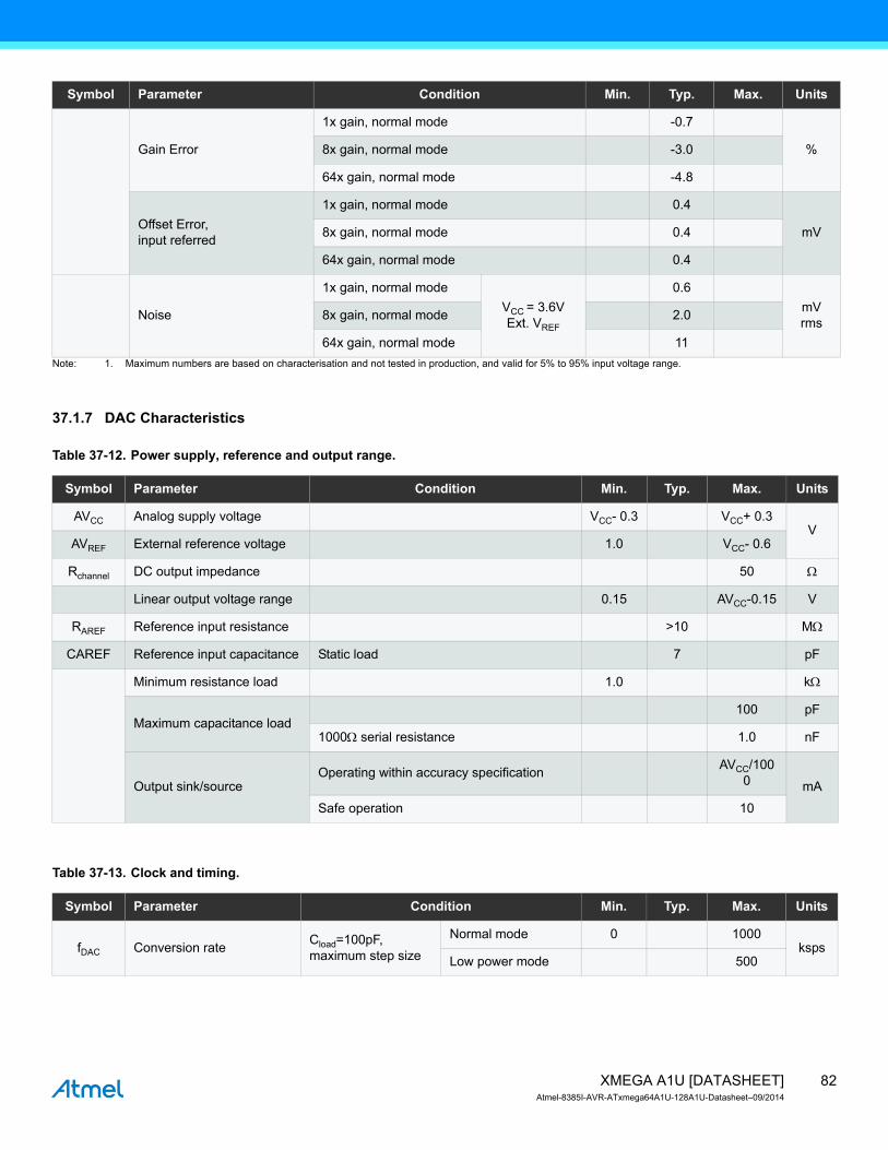
82XMEGA A1U [DATASHEET]Atmel-8385I-AVR-ATxmega64A1U-128A1U-Datasheet–09/2014
Note: 1. Maximum numbers are based on characterisation and not tested in production, and valid for 5% to 95% input voltage range.
37.1.7 DAC Characteristics
Table 37-12. Power supply, reference and output range.
Table 37-13. Clock and timing.
Gain Error
1x gain, normal mode -0.7
%8x gain, normal mode -3.0
64x gain, normal mode -4.8
Offset Error,input referred
1x gain, normal mode 0.4
mV8x gain, normal mode 0.4
64x gain, normal mode 0.4
Noise
1x gain, normal modeVCC = 3.6VExt. VREF
0.6mVrms8x gain, normal mode 2.0
64x gain, normal mode 11
Symbol Parameter Condition Min. Typ. Max. Units
Symbol Parameter Condition Min. Typ. Max. Units
AVCC Analog supply voltage VCC- 0.3 VCC+ 0.3V
AVREF External reference voltage 1.0 VCC- 0.6
Rchannel DC output impedance 50 Ω
Linear output voltage range 0.15 AVCC-0.15 V
RAREF Reference input resistance >10 MΩ
CAREF Reference input capacitance Static load 7 pF
Minimum resistance load 1.0 kΩ
Maximum capacitance load100 pF
1000Ω serial resistance 1.0 nF
Output sink/sourceOperating within accuracy specification AVCC/100
0 mA
Safe operation 10
Symbol Parameter Condition Min. Typ. Max. Units
fDAC Conversion rate Cload=100pF, maximum step size
Normal mode 0 1000ksps
Low power mode 500
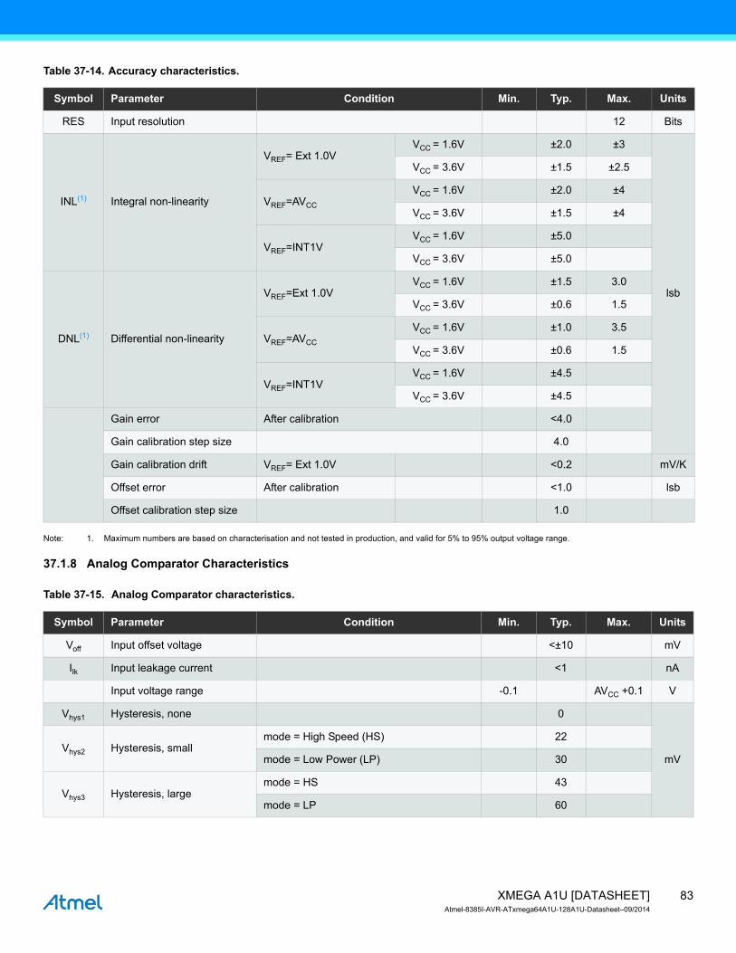
83XMEGA A1U [DATASHEET]Atmel-8385I-AVR-ATxmega64A1U-128A1U-Datasheet–09/2014
Table 37-14. Accuracy characteristics.
Note: 1. Maximum numbers are based on characterisation and not tested in production, and valid for 5% to 95% output voltage range.
37.1.8 Analog Comparator Characteristics
Table 37-15. Analog Comparator characteristics.
Symbol Parameter Condition Min. Typ. Max. Units
RES Input resolution 12 Bits
INL(1) Integral non-linearity
VREF= Ext 1.0VVCC = 1.6V ±2.0 ±3
lsb
VCC = 3.6V ±1.5 ±2.5
VREF=AVCC
VCC = 1.6V ±2.0 ±4
VCC = 3.6V ±1.5 ±4
VREF=INT1VVCC = 1.6V ±5.0
VCC = 3.6V ±5.0
DNL(1) Differential non-linearity
VREF=Ext 1.0VVCC = 1.6V ±1.5 3.0
VCC = 3.6V ±0.6 1.5
VREF=AVCC
VCC = 1.6V ±1.0 3.5
VCC = 3.6V ±0.6 1.5
VREF=INT1VVCC = 1.6V ±4.5
VCC = 3.6V ±4.5
Gain error After calibration <4.0
Gain calibration step size 4.0
Gain calibration drift VREF= Ext 1.0V <0.2 mV/K
Offset error After calibration <1.0 lsb
Offset calibration step size 1.0
Symbol Parameter Condition Min. Typ. Max. Units
Voff Input offset voltage <±10 mV
Ilk Input leakage current <1 nA
Input voltage range -0.1 AVCC +0.1 V
Vhys1 Hysteresis, none 0
mVVhys2 Hysteresis, small
mode = High Speed (HS) 22
mode = Low Power (LP) 30
Vhys3 Hysteresis, largemode = HS 43
mode = LP 60
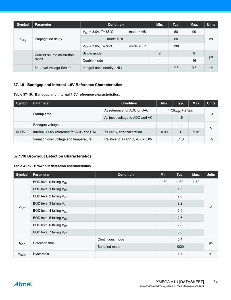
84XMEGA A1U [DATASHEET]Atmel-8385I-AVR-ATxmega64A1U-128A1U-Datasheet–09/2014
37.1.9 Bandgap and Internal 1.0V Reference Characteristics
Table 37-16. Bandgap and Internal 1.0V reference characteristics.
37.1.10 Brownout Detection Characteristics
Table 37-17. Brownout detection characteristics.
tdelay Propagation delay
VCC = 3.0V, T= 85°C mode = HS 60 90
nsmode = HS 60
VCC = 3.0V, T= 85°C mode = LP 130
Current source calibration range
Single mode 2 8µs
Double mode 4 16
64-Level Voltage Scaler Integral non-linearity (INL) 0.3 0.5 lsb
Symbol Parameter Condition Min. Typ. Max. Units
Symbol Parameter Condition Min. Typ. Max. Units
Startup timeAs reference for ADC or DAC 1 ClkPER + 2.5µs
µsAs input voltage to ADC and AC 1.5
Bandgap voltage 1.1V
INT1V Internal 1.00V reference for ADC and DAC T= 85°C, after calibration 0.99 1 1.01
Variation over voltage and temperature Relative to T= 85°C, VCC = 3.0V ±1.0 %
Symbol Parameter Condition Min. Typ. Max. Units
VBOT
BOD level 0 falling VCC 1.60 1.62 1.72
V
BOD level 1 falling VCC 1.8
BOD level 2 falling VCC 2.0
BOD level 3 falling VCC 2.2
BOD level 4 falling VCC 2.4
BOD level 5 falling VCC 2.6
BOD level 6 falling VCC 2.8
BOD level 7 falling VCC 3.0
tBOD Detection timeContinuous mode 0.4
µsSampled mode 1000
VHYST Hysteresis 1.4 %
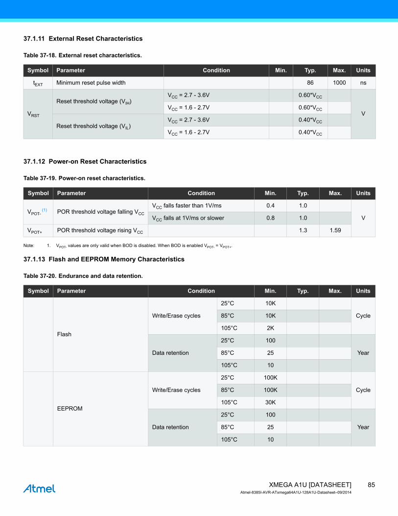
85XMEGA A1U [DATASHEET]Atmel-8385I-AVR-ATxmega64A1U-128A1U-Datasheet–09/2014
37.1.11 External Reset Characteristics
Table 37-18. External reset characteristics.
37.1.12 Power-on Reset Characteristics
Table 37-19. Power-on reset characteristics.
Note: 1. VPOT- values are only valid when BOD is disabled. When BOD is enabled VPOT- = VPOT+.
37.1.13 Flash and EEPROM Memory Characteristics
Table 37-20. Endurance and data retention.
Symbol Parameter Condition Min. Typ. Max. Units
tEXT Minimum reset pulse width 86 1000 ns
VRST
Reset threshold voltage (VIH)VCC = 2.7 - 3.6V 0.60*VCC
VVCC = 1.6 - 2.7V 0.60*VCC
Reset threshold voltage (VIL)VCC = 2.7 - 3.6V 0.40*VCC
VCC = 1.6 - 2.7V 0.40*VCC
Symbol Parameter Condition Min. Typ. Max. Units
VPOT- (1) POR threshold voltage falling VCC
VCC falls faster than 1V/ms 0.4 1.0
VVCC falls at 1V/ms or slower 0.8 1.0
VPOT+ POR threshold voltage rising VCC 1.3 1.59
Symbol Parameter Condition Min. Typ. Max. Units
Flash
Write/Erase cycles
25°C 10K
Cycle85°C 10K
105°C 2K
Data retention
25°C 100
Year85°C 25
105°C 10
EEPROM
Write/Erase cycles
25°C 100K
Cycle85°C 100K
105°C 30K
Data retention
25°C 100
Year85°C 25
105°C 10

86XMEGA A1U [DATASHEET]Atmel-8385I-AVR-ATxmega64A1U-128A1U-Datasheet–09/2014
Table 37-21. Programming time.
Notes: 1. Programming is timed from the 2MHz internal oscillator.2. EEPROM is not erased if the EESAVE fuse is programmed.
37.1.14 Clock and Oscillator Characteristics
37.1.14.1 Calibrated 32.768kHz Internal Oscillator characteristics
Table 37-22. 32.768kHz internal oscillator characteristics.
37.1.14.2 Calibrated 2MHz RC Internal Oscillator characteristics
Table 37-23. 2MHz internal oscillator characteristics.
Symbol Parameter Condition Min. Typ. (1) Max. Units
Chip Erase 64KB Flash, EEPROM(2) and SRAM Erase 55
ms
Flash
Page Erase 4
Page Write 4
Atomic Page Erase and Write 8
EEPROM
Page Erase 4
Page Write 4
Atomic Page Erase and Write 8
Symbol Parameter Condition Min. Typ. Max. Units
Frequency 32.768 kHz
Factory calibration accuracy T = 85°C, VCC = 3.0V -0.5 0.5%
User calibration accuracy -0.5 0.5
Symbol Parameter Condition Min. Typ. Max. Units
Tunable frequency range DFLL can tune to this frequency over voltage and temperature 1.8 2.2
MHz
Factory calibrated frequency 2.0
Factory calibration accuracy T = 85°C, VCC= 3.0V -1.5 1.5%
DFLL calibration stepsize T = 25°C, VCC= 3.0V 0.23

87XMEGA A1U [DATASHEET]Atmel-8385I-AVR-ATxmega64A1U-128A1U-Datasheet–09/2014
37.1.14.3 Calibrated and tunable 32MHz internal oscillator characteristics
Table 37-24. 32MHz internal oscillator characteristics.
37.1.14.4 32kHz Internal ULP Oscillator characteristics
Table 37-25. 32kHz internal ULP oscillator characteristics.
37.1.14.5 Internal Phase Locked Loop (PLL) characteristics
Table 37-26. Internal PLL characteristics.
Note: 1. The maximum output frequency vs. supply voltage is linear between 1.8V and 2.7V, and can never be higher than four times the maximum CPU frequency.
Symbol Parameter Condition Min. Typ. Max. Units
Tunable frequency range DFLL can tune to this frequency over voltage and temperature 30 35
MHz
Factory calibrated frequency 32
Factory calibration accuracy T = 85°C, VCC= 3.0V -1.5 1.5%
DFLL calibration step size 0.24
Symbol Parameter Condition Min. Typ. Max. Units
Output frequency 32 kHz
Accuracy -30 30 %
Symbol Parameter Condition Min. Typ. Max. Units
fIN Input frequency Output frequency must be within fOUT 0.4 64
MHzfOUT Output frequency(1)
VCC= 1.6V 20 32
VCC= 2.7V 20 96
VCC= 3.6V 20 128
Duty cycle 50 %
Start-up lock time fOUT = 48MHz 18µs
Re-lock time fOUT-init = 10MHz, fOUT-end = 64MHz 17
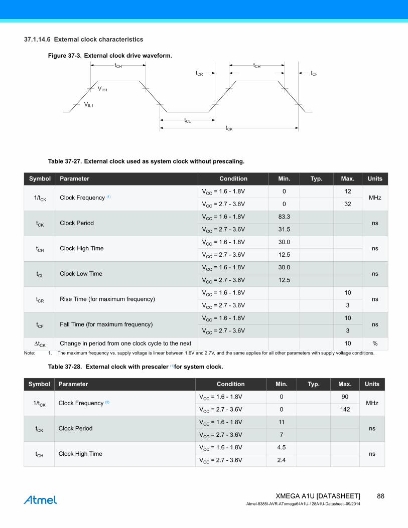
88XMEGA A1U [DATASHEET]Atmel-8385I-AVR-ATxmega64A1U-128A1U-Datasheet–09/2014
37.1.14.6 External clock characteristics
Figure 37-3. External clock drive waveform.
Table 37-27. External clock used as system clock without prescaling.
Note: 1. The maximum frequency vs. supply voltage is linear between 1.6V and 2.7V, and the same applies for all other parameters with supply voltage conditions.
Table 37-28. External clock with prescaler (1)for system clock.
tCH
tCL
tCK
tCH
VIL1
VIH1
tCR tCF
Symbol Parameter Condition Min. Typ. Max. Units
1/tCK Clock Frequency (1)VCC = 1.6 - 1.8V 0 12
MHzVCC = 2.7 - 3.6V 0 32
tCK Clock PeriodVCC = 1.6 - 1.8V 83.3
nsVCC = 2.7 - 3.6V 31.5
tCH Clock High TimeVCC = 1.6 - 1.8V 30.0
nsVCC = 2.7 - 3.6V 12.5
tCL Clock Low TimeVCC = 1.6 - 1.8V 30.0
nsVCC = 2.7 - 3.6V 12.5
tCR Rise Time (for maximum frequency)VCC = 1.6 - 1.8V 10
nsVCC = 2.7 - 3.6V 3
tCF Fall Time (for maximum frequency)VCC = 1.6 - 1.8V 10
nsVCC = 2.7 - 3.6V 3
ΔtCK Change in period from one clock cycle to the next 10 %
Symbol Parameter Condition Min. Typ. Max. Units
1/tCK Clock Frequency (2)VCC = 1.6 - 1.8V 0 90
MHzVCC = 2.7 - 3.6V 0 142
tCK Clock PeriodVCC = 1.6 - 1.8V 11
nsVCC = 2.7 - 3.6V 7
tCH Clock High TimeVCC = 1.6 - 1.8V 4.5
nsVCC = 2.7 - 3.6V 2.4
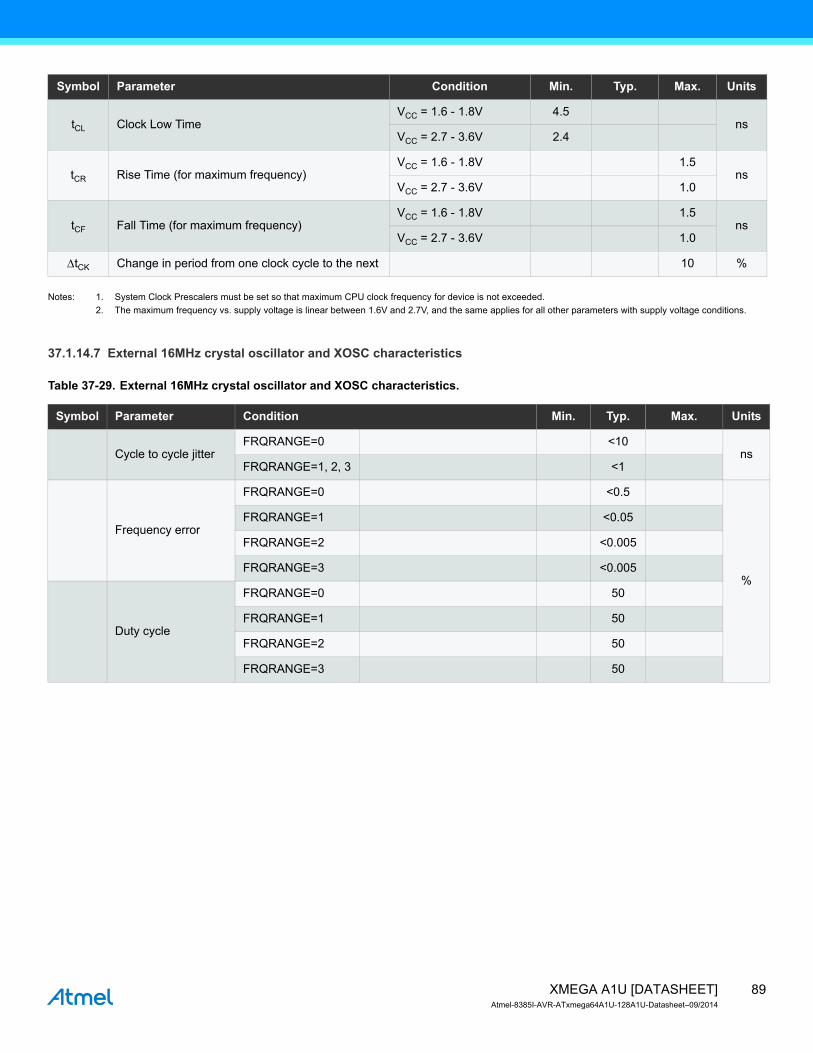
89XMEGA A1U [DATASHEET]Atmel-8385I-AVR-ATxmega64A1U-128A1U-Datasheet–09/2014
Notes: 1. System Clock Prescalers must be set so that maximum CPU clock frequency for device is not exceeded.2. The maximum frequency vs. supply voltage is linear between 1.6V and 2.7V, and the same applies for all other parameters with supply voltage conditions.
37.1.14.7 External 16MHz crystal oscillator and XOSC characteristics
Table 37-29. External 16MHz crystal oscillator and XOSC characteristics..
tCL Clock Low TimeVCC = 1.6 - 1.8V 4.5
nsVCC = 2.7 - 3.6V 2.4
tCR Rise Time (for maximum frequency)VCC = 1.6 - 1.8V 1.5
nsVCC = 2.7 - 3.6V 1.0
tCF Fall Time (for maximum frequency)VCC = 1.6 - 1.8V 1.5
nsVCC = 2.7 - 3.6V 1.0
ΔtCK Change in period from one clock cycle to the next 10 %
Symbol Parameter Condition Min. Typ. Max. Units
Symbol Parameter Condition Min. Typ. Max. Units
Cycle to cycle jitterFRQRANGE=0 <10
nsFRQRANGE=1, 2, 3 <1
Frequency error
FRQRANGE=0 <0.5
%
FRQRANGE=1 <0.05
FRQRANGE=2 <0.005
FRQRANGE=3 <0.005
Duty cycle
FRQRANGE=0 50
FRQRANGE=1 50
FRQRANGE=2 50
FRQRANGE=3 50
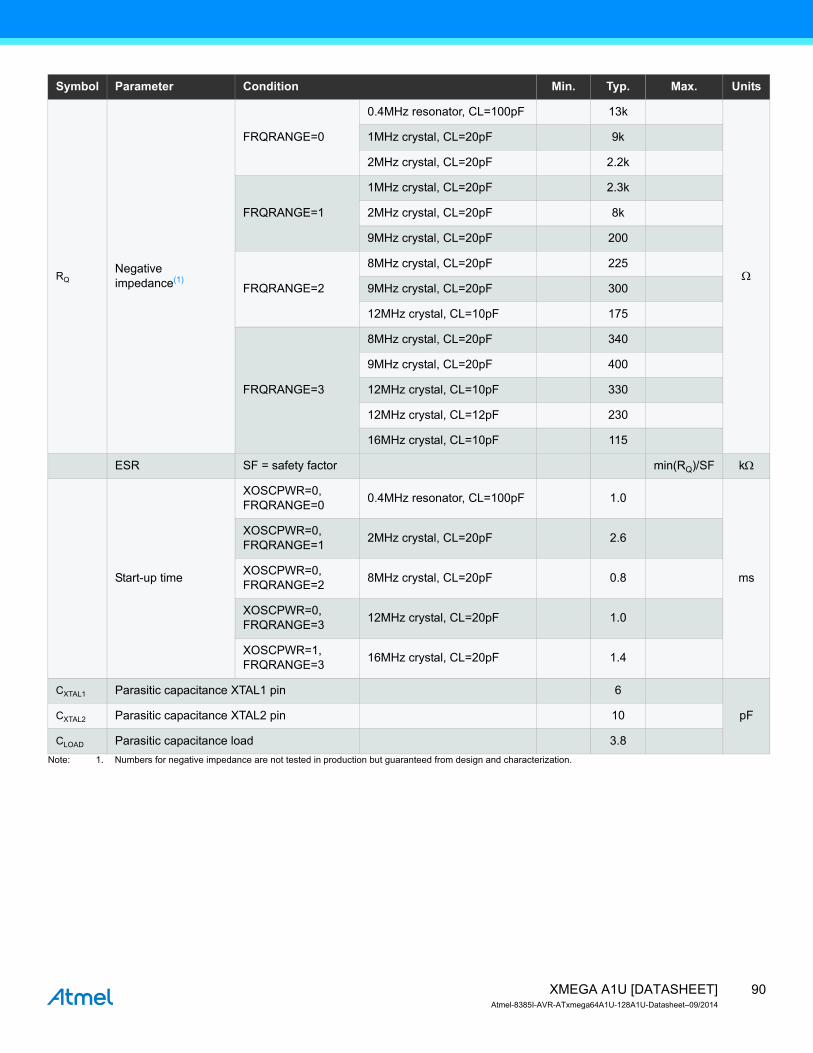
90XMEGA A1U [DATASHEET]Atmel-8385I-AVR-ATxmega64A1U-128A1U-Datasheet–09/2014
Note: 1. Numbers for negative impedance are not tested in production but guaranteed from design and characterization.
RQNegative impedance(1)
FRQRANGE=0
0.4MHz resonator, CL=100pF 13k
Ω
1MHz crystal, CL=20pF 9k
2MHz crystal, CL=20pF 2.2k
FRQRANGE=1
1MHz crystal, CL=20pF 2.3k
2MHz crystal, CL=20pF 8k
9MHz crystal, CL=20pF 200
FRQRANGE=2
8MHz crystal, CL=20pF 225
9MHz crystal, CL=20pF 300
12MHz crystal, CL=10pF 175
FRQRANGE=3
8MHz crystal, CL=20pF 340
9MHz crystal, CL=20pF 400
12MHz crystal, CL=10pF 330
12MHz crystal, CL=12pF 230
16MHz crystal, CL=10pF 115
ESR SF = safety factor min(RQ)/SF kΩ
Start-up time
XOSCPWR=0,FRQRANGE=0 0.4MHz resonator, CL=100pF 1.0
ms
XOSCPWR=0,FRQRANGE=1 2MHz crystal, CL=20pF 2.6
XOSCPWR=0,FRQRANGE=2 8MHz crystal, CL=20pF 0.8
XOSCPWR=0,FRQRANGE=3 12MHz crystal, CL=20pF 1.0
XOSCPWR=1,FRQRANGE=3 16MHz crystal, CL=20pF 1.4
CXTAL1 Parasitic capacitance XTAL1 pin 6
pFCXTAL2 Parasitic capacitance XTAL2 pin 10
CLOAD Parasitic capacitance load 3.8
Symbol Parameter Condition Min. Typ. Max. Units
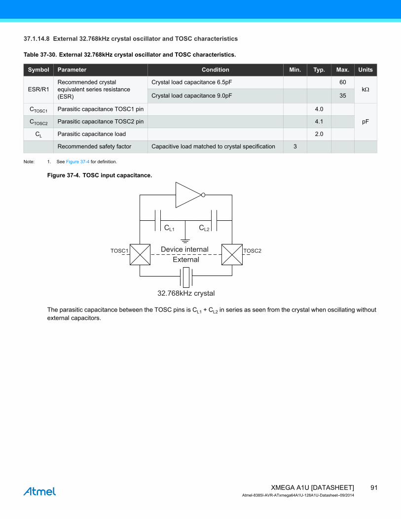
91XMEGA A1U [DATASHEET]Atmel-8385I-AVR-ATxmega64A1U-128A1U-Datasheet–09/2014
37.1.14.8 External 32.768kHz crystal oscillator and TOSC characteristics
Table 37-30. External 32.768kHz crystal oscillator and TOSC characteristics.
Note: 1. See Figure 37-4 for definition.
Figure 37-4. TOSC input capacitance.
The parasitic capacitance between the TOSC pins is CL1 + CL2 in series as seen from the crystal when oscillating without external capacitors.
Symbol Parameter Condition Min. Typ. Max. Units
ESR/R1Recommended crystal equivalent series resistance (ESR)
Crystal load capacitance 6.5pF 60kΩ
Crystal load capacitance 9.0pF 35
CTOSC1 Parasitic capacitance TOSC1 pin 4.0
pFCTOSC2 Parasitic capacitance TOSC2 pin 4.1
CL Parasitic capacitance load 2.0
Recommended safety factor Capacitive load matched to crystal specification 3
CL1 CL2
2CSOT1CSOT Device internalExternal
32.768kHz crystal
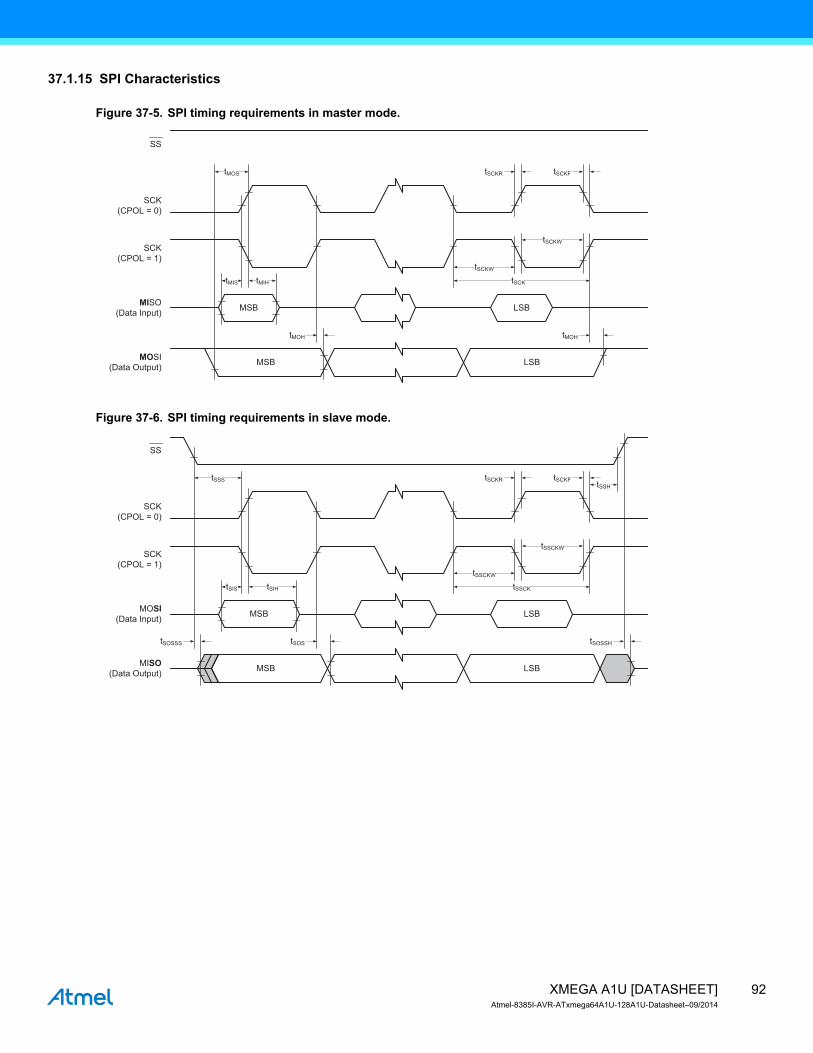
92XMEGA A1U [DATASHEET]Atmel-8385I-AVR-ATxmega64A1U-128A1U-Datasheet–09/2014
37.1.15 SPI Characteristics
Figure 37-5. SPI timing requirements in master mode.
Figure 37-6. SPI timing requirements in slave mode.
MSB LSB
BSLBSM
tMOS
tMIS tMIH
tSCKW
tSCK
tMOH tMOH
tSCKFtSCKR
tSCKW
MOSI(Data Output)
MISO(Data Input)
SCK(CPOL = 1)
SCK(CPOL = 0)
SS
MSB LSB
BSLBSM
tSIS tSIH
tSSCKW
tSSCKW
tSSCK
tSSH
tSOSSH
tSCKR tSCKF
tSOS
tSSS
tSOSSS
MISO(Data Output)
MOSI(Data Input)
SCK(CPOL = 1)
SCK(CPOL = 0)
SS
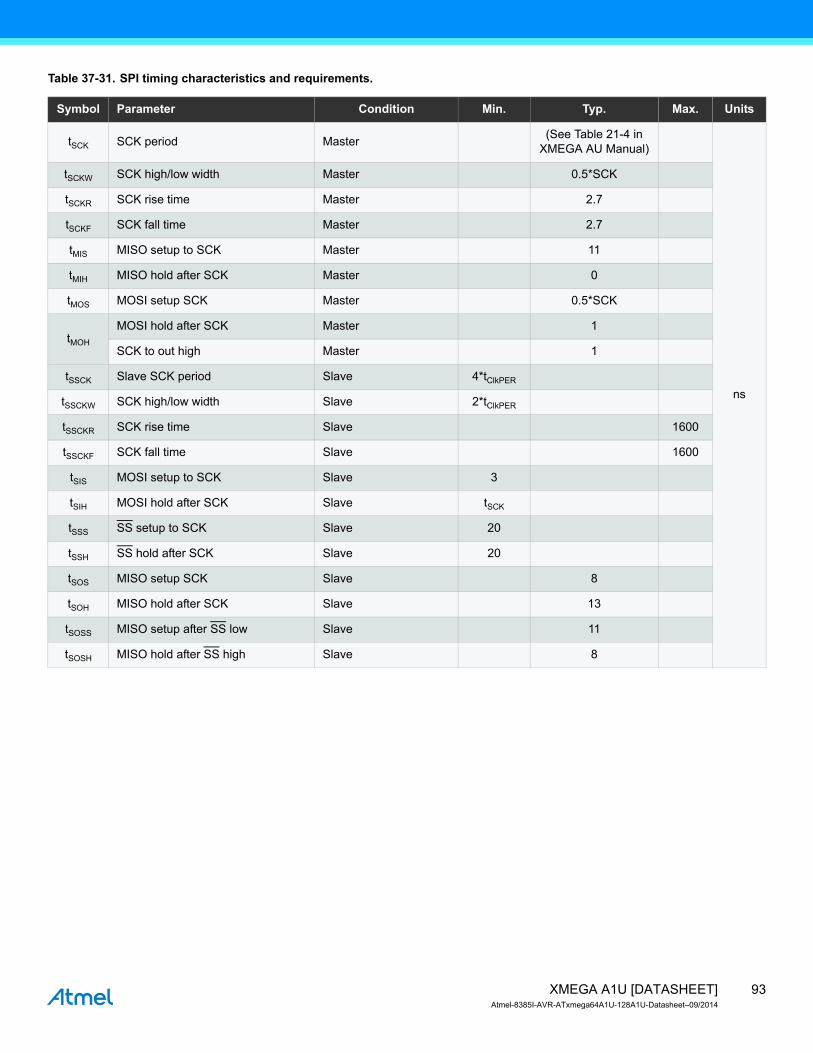
93XMEGA A1U [DATASHEET]Atmel-8385I-AVR-ATxmega64A1U-128A1U-Datasheet–09/2014
Table 37-31. SPI timing characteristics and requirements.
Symbol Parameter Condition Min. Typ. Max. Units
tSCK SCK period Master (See Table 21-4 in XMEGA AU Manual)
ns
tSCKW SCK high/low width Master 0.5*SCK
tSCKR SCK rise time Master 2.7
tSCKF SCK fall time Master 2.7
tMIS MISO setup to SCK Master 11
tMIH MISO hold after SCK Master 0
tMOS MOSI setup SCK Master 0.5*SCK
tMOH
MOSI hold after SCK Master 1
SCK to out high Master 1
tSSCK Slave SCK period Slave 4*tClkPER
tSSCKW SCK high/low width Slave 2*tClkPER
tSSCKR SCK rise time Slave 1600
tSSCKF SCK fall time Slave 1600
tSIS MOSI setup to SCK Slave 3
tSIH MOSI hold after SCK Slave tSCK
tSSS SS setup to SCK Slave 20
tSSH SS hold after SCK Slave 20
tSOS MISO setup SCK Slave 8
tSOH MISO hold after SCK Slave 13
tSOSS MISO setup after SS low Slave 11
tSOSH MISO hold after SS high Slave 8
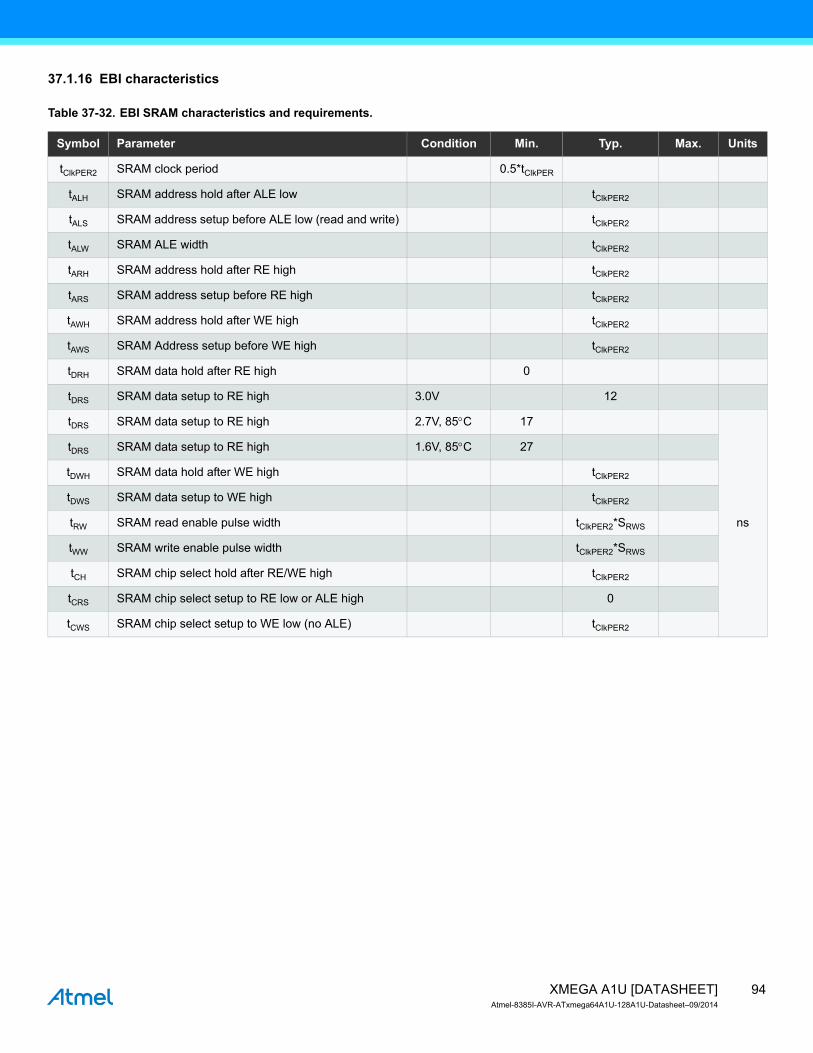
94XMEGA A1U [DATASHEET]Atmel-8385I-AVR-ATxmega64A1U-128A1U-Datasheet–09/2014
37.1.16 EBI characteristics
Table 37-32. EBI SRAM characteristics and requirements.
Symbol Parameter Condition Min. Typ. Max. Units
tClkPER2 SRAM clock period 0.5*tClkPER
tALH SRAM address hold after ALE low tClkPER2
tALS SRAM address setup before ALE low (read and write) tClkPER2
tALW SRAM ALE width tClkPER2
tARH SRAM address hold after RE high tClkPER2
tARS SRAM address setup before RE high tClkPER2
tAWH SRAM address hold after WE high tClkPER2
tAWS SRAM Address setup before WE high tClkPER2
tDRH SRAM data hold after RE high 0
tDRS SRAM data setup to RE high 3.0V 12
tDRS SRAM data setup to RE high 2.7V, 85°C 17
ns
tDRS SRAM data setup to RE high 1.6V, 85°C 27
tDWH SRAM data hold after WE high tClkPER2
tDWS SRAM data setup to WE high tClkPER2
tRW SRAM read enable pulse width tClkPER2*SRWS
tWW SRAM write enable pulse width tClkPER2*SRWS
tCH SRAM chip select hold after RE/WE high tClkPER2
tCRS SRAM chip select setup to RE low or ALE high 0
tCWS SRAM chip select setup to WE low (no ALE) tClkPER2
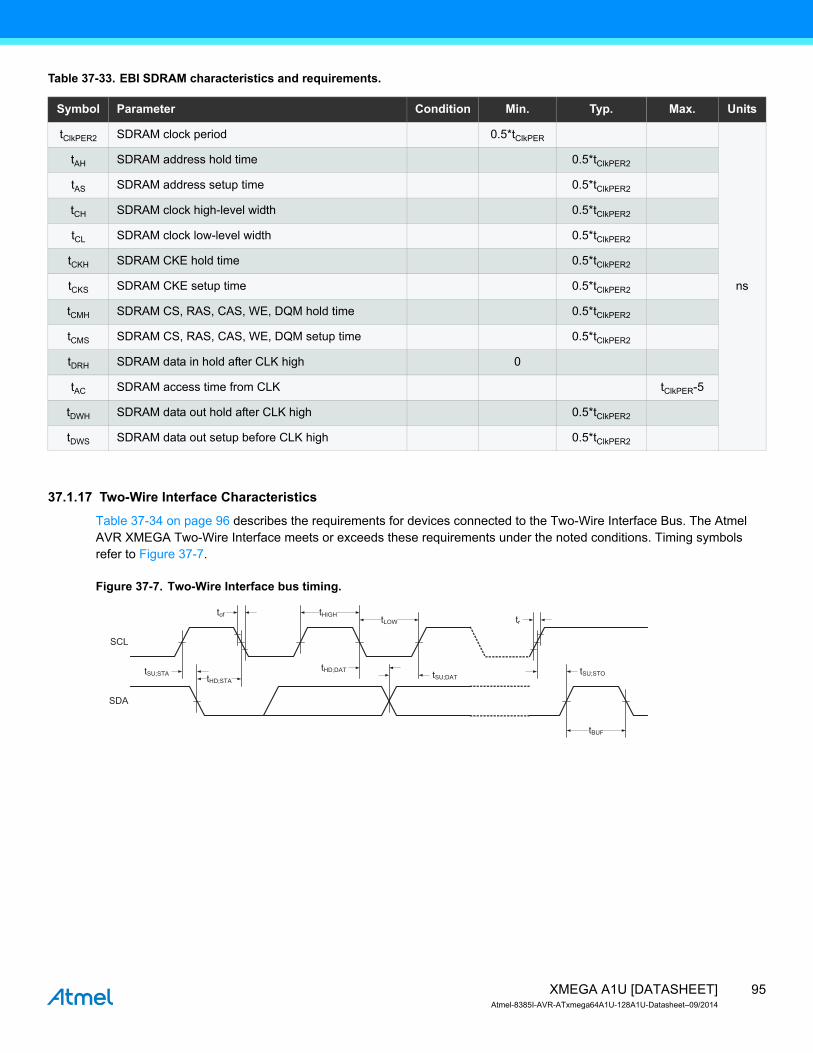
95XMEGA A1U [DATASHEET]Atmel-8385I-AVR-ATxmega64A1U-128A1U-Datasheet–09/2014
Table 37-33. EBI SDRAM characteristics and requirements.
37.1.17 Two-Wire Interface Characteristics
Table 37-34 on page 96 describes the requirements for devices connected to the Two-Wire Interface Bus. The Atmel AVR XMEGA Two-Wire Interface meets or exceeds these requirements under the noted conditions. Timing symbols refer to Figure 37-7.
Figure 37-7. Two-Wire Interface bus timing.
Symbol Parameter Condition Min. Typ. Max. Units
tClkPER2 SDRAM clock period 0.5*tClkPER
ns
tAH SDRAM address hold time 0.5*tClkPER2
tAS SDRAM address setup time 0.5*tClkPER2
tCH SDRAM clock high-level width 0.5*tClkPER2
tCL SDRAM clock low-level width 0.5*tClkPER2
tCKH SDRAM CKE hold time 0.5*tClkPER2
tCKS SDRAM CKE setup time 0.5*tClkPER2
tCMH SDRAM CS, RAS, CAS, WE, DQM hold time 0.5*tClkPER2
tCMS SDRAM CS, RAS, CAS, WE, DQM setup time 0.5*tClkPER2
tDRH SDRAM data in hold after CLK high 0
tAC SDRAM access time from CLK tClkPER-5
tDWH SDRAM data out hold after CLK high 0.5*tClkPER2
tDWS SDRAM data out setup before CLK high 0.5*tClkPER2
tHD;STA
tof
SDA
SCL
tLOWtHIGH
tSU;STA
tBUF
tr
tHD;DAT tSU;DATtSU;STO
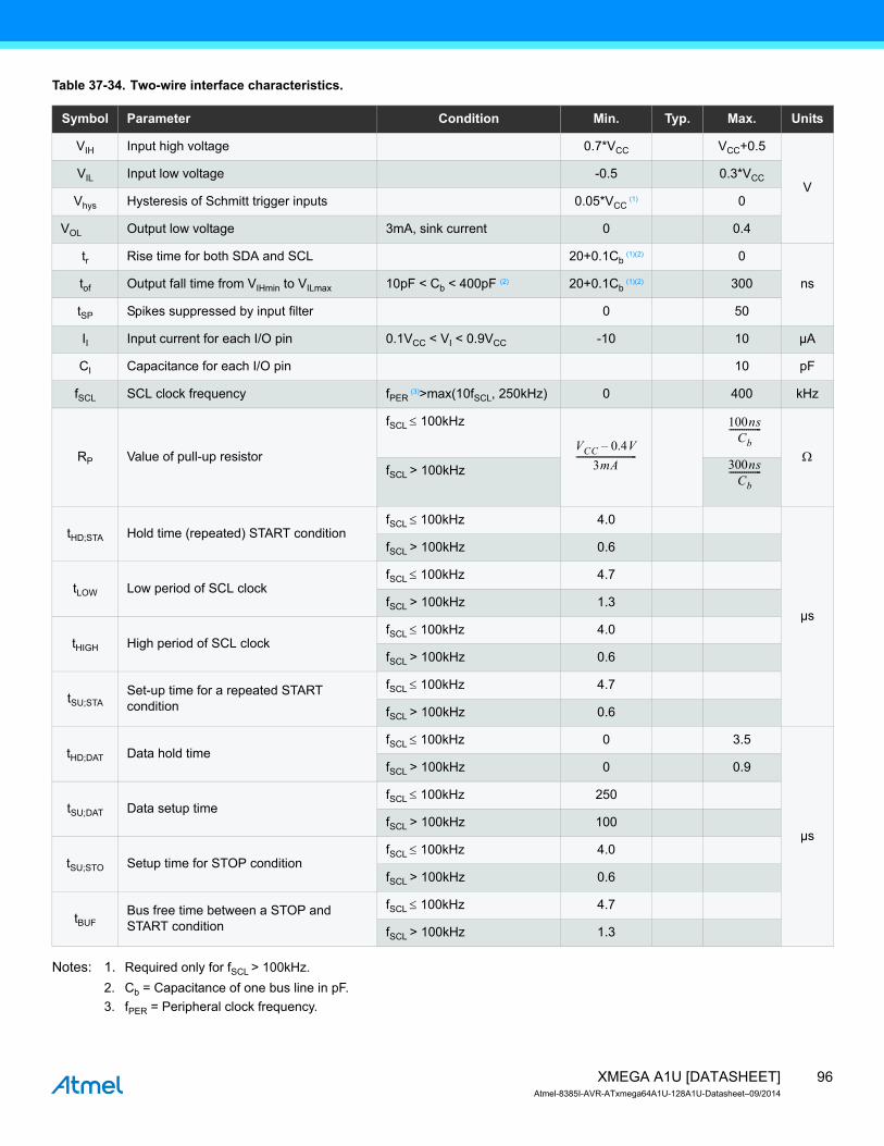
96XMEGA A1U [DATASHEET]Atmel-8385I-AVR-ATxmega64A1U-128A1U-Datasheet–09/2014
Table 37-34. Two-wire interface characteristics.
Notes: 1. Required only for fSCL > 100kHz.2. Cb = Capacitance of one bus line in pF.3. fPER = Peripheral clock frequency.
Symbol Parameter Condition Min. Typ. Max. Units
VIH Input high voltage 0.7*VCC VCC+0.5
VVIL Input low voltage -0.5 0.3*VCC
Vhys Hysteresis of Schmitt trigger inputs 0.05*VCC (1) 0
VOL Output low voltage 3mA, sink current 0 0.4
tr Rise time for both SDA and SCL 20+0.1Cb (1)(2) 0
nstof Output fall time from VIHmin to VILmax 10pF < Cb < 400pF (2) 20+0.1Cb (1)(2) 300
tSP Spikes suppressed by input filter 0 50
II Input current for each I/O pin 0.1VCC < VI < 0.9VCC -10 10 µA
CI Capacitance for each I/O pin 10 pF
fSCL SCL clock frequency fPER (3)>max(10fSCL, 250kHz) 0 400 kHz
RP Value of pull-up resistor
fSCL ≤ 100kHz
ΩfSCL > 100kHz
tHD;STA Hold time (repeated) START conditionfSCL ≤ 100kHz 4.0
µs
fSCL > 100kHz 0.6
tLOW Low period of SCL clockfSCL ≤ 100kHz 4.7
fSCL > 100kHz 1.3
tHIGH High period of SCL clockfSCL ≤ 100kHz 4.0
fSCL > 100kHz 0.6
tSU;STASet-up time for a repeated START condition
fSCL ≤ 100kHz 4.7
fSCL > 100kHz 0.6
tHD;DAT Data hold timefSCL ≤ 100kHz 0 3.5
µs
fSCL > 100kHz 0 0.9
tSU;DAT Data setup timefSCL ≤ 100kHz 250
fSCL > 100kHz 100
tSU;STO Setup time for STOP conditionfSCL ≤ 100kHz 4.0
fSCL > 100kHz 0.6
tBUFBus free time between a STOP and START condition
fSCL ≤ 100kHz 4.7
fSCL > 100kHz 1.3
VCC 0.4V–3mA
----------------------------
100nsCb---------------
300nsCb---------------
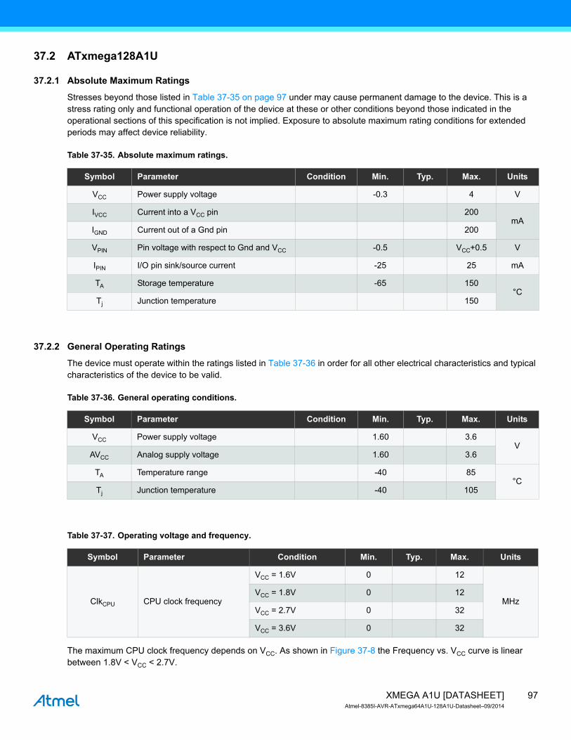
97XMEGA A1U [DATASHEET]Atmel-8385I-AVR-ATxmega64A1U-128A1U-Datasheet–09/2014
37.2 ATxmega128A1U
37.2.1 Absolute Maximum Ratings
Stresses beyond those listed in Table 37-35 on page 97 under may cause permanent damage to the device. This is a stress rating only and functional operation of the device at these or other conditions beyond those indicated in the operational sections of this specification is not implied. Exposure to absolute maximum rating conditions for extended periods may affect device reliability.
Table 37-35. Absolute maximum ratings.
37.2.2 General Operating Ratings
The device must operate within the ratings listed in Table 37-36 in order for all other electrical characteristics and typical characteristics of the device to be valid.
Table 37-36. General operating conditions.
Table 37-37. Operating voltage and frequency.
The maximum CPU clock frequency depends on VCC. As shown in Figure 37-8 the Frequency vs. VCC curve is linear between 1.8V < VCC < 2.7V.
Symbol Parameter Condition Min. Typ. Max. Units
VCC Power supply voltage -0.3 4 V
IVCC Current into a VCC pin 200mA
IGND Current out of a Gnd pin 200
VPIN Pin voltage with respect to Gnd and VCC -0.5 VCC+0.5 V
IPIN I/O pin sink/source current -25 25 mA
TA Storage temperature -65 150°C
Tj Junction temperature 150
Symbol Parameter Condition Min. Typ. Max. Units
VCC Power supply voltage 1.60 3.6V
AVCC Analog supply voltage 1.60 3.6
TA Temperature range -40 85°C
Tj Junction temperature -40 105
Symbol Parameter Condition Min. Typ. Max. Units
ClkCPU CPU clock frequency
VCC = 1.6V 0 12
MHzVCC = 1.8V 0 12
VCC = 2.7V 0 32
VCC = 3.6V 0 32
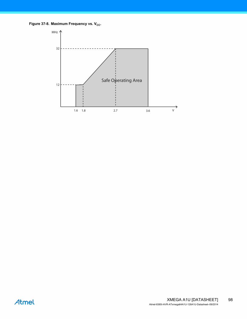
98XMEGA A1U [DATASHEET]Atmel-8385I-AVR-ATxmega64A1U-128A1U-Datasheet–09/2014
Figure 37-8. Maximum Frequency vs. VCC.
1.8
12
32
MHz
V2.7 3.61.6
Safe Operating Area
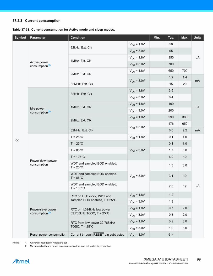
99XMEGA A1U [DATASHEET]Atmel-8385I-AVR-ATxmega64A1U-128A1U-Datasheet–09/2014
37.2.3 Current consumption
Table 37-38. Current consumption for Active mode and sleep modes.
Notes: 1. All Power Reduction Registers set.2. Maximum limits are based on characterization, and not tested in production.
Symbol Parameter Condition Min. Typ. Max. Units
ICC
Active power consumption(1)
32kHz, Ext. ClkVCC = 1.8V 50
µA
VCC = 3.0V 95
1MHz, Ext. ClkVCC = 1.8V 350
VCC = 3.0V 700
2MHz, Ext. ClkVCC = 1.8V 650 700
VCC = 3.0V1.2 1.4
mA32MHz, Ext. Clk 15 20
Idle powerconsumption(1)
32kHz, Ext. ClkVCC = 1.8V 3.5
µA
VCC = 3.0V 6.4
1MHz, Ext. ClkVCC = 1.8V 109
VCC = 3.0V 200
2MHz, Ext. ClkVCC = 1.8V 290 380
VCC = 3.0V476 650
32MHz, Ext. Clk 6.6 9.2 mA
Power-down power consumption
T = 25°C VCC = 1.8V 0.1 1.0
µA
T = 25°C
VCC = 3.0V
0.1 1.0
T = 85°C 1.7 5.0
T = 105°C 6.0 10
WDT and sampled BOD enabled,T = 25°C
VCC = 3.0V
1.3 3.0
WDT and sampled BOD enabled,T = 85°C 3.1 10
WDT and sampled BOD enabled,T = 105°C 7.0 12
Power-save power consumption(2)
RTC on ULP clock, WDT andsampled BOD enabled, T = 25°C
VCC = 1.8V 1.2
VCC = 3.0V 1.3
RTC on 1.024kHz low power32.768kHz TOSC, T = 25°C
VCC = 1.8V 0.7 2.0
VCC = 3.0V 0.8 2.0
RTC from low power 32.768kHzTOSC, T = 25°C
VCC = 1.8V 0.9 3.0
VCC = 3.0V 1.0 3.0
Reset power consumption Current through RESET pin subtracted VCC = 3.0V 914
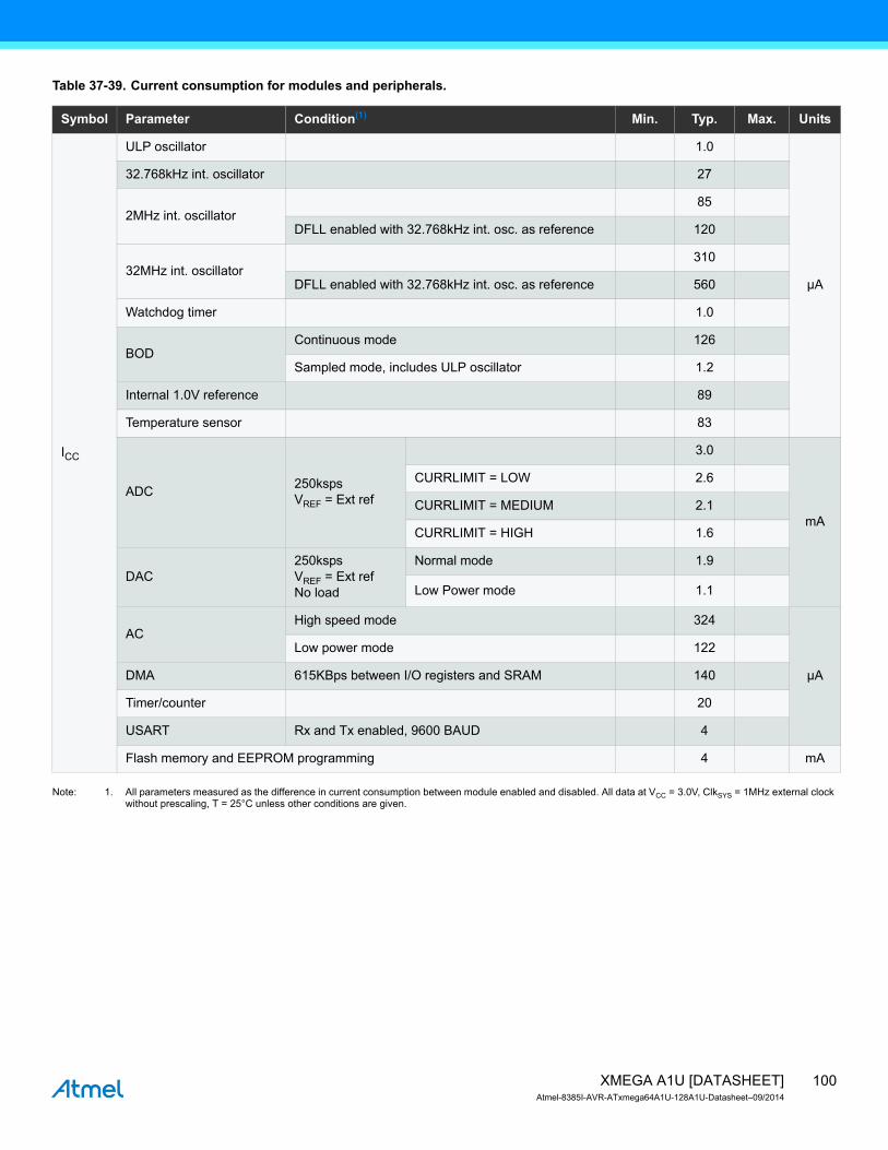
100XMEGA A1U [DATASHEET]Atmel-8385I-AVR-ATxmega64A1U-128A1U-Datasheet–09/2014
Table 37-39. Current consumption for modules and peripherals.
Note: 1. All parameters measured as the difference in current consumption between module enabled and disabled. All data at VCC = 3.0V, ClkSYS = 1MHz external clock without prescaling, T = 25°C unless other conditions are given.
Symbol Parameter Condition(1) Min. Typ. Max. Units
ICC
ULP oscillator 1.0
µA
32.768kHz int. oscillator 27
2MHz int. oscillator85
DFLL enabled with 32.768kHz int. osc. as reference 120
32MHz int. oscillator310
DFLL enabled with 32.768kHz int. osc. as reference 560
Watchdog timer 1.0
BODContinuous mode 126
Sampled mode, includes ULP oscillator 1.2
Internal 1.0V reference 89
Temperature sensor 83
ADC 250kspsVREF = Ext ref
3.0
mA
CURRLIMIT = LOW 2.6
CURRLIMIT = MEDIUM 2.1
CURRLIMIT = HIGH 1.6
DAC250kspsVREF = Ext refNo load
Normal mode 1.9
Low Power mode 1.1
ACHigh speed mode 324
µA
Low power mode 122
DMA 615KBps between I/O registers and SRAM 140
Timer/counter 20
USART Rx and Tx enabled, 9600 BAUD 4
Flash memory and EEPROM programming 4 mA
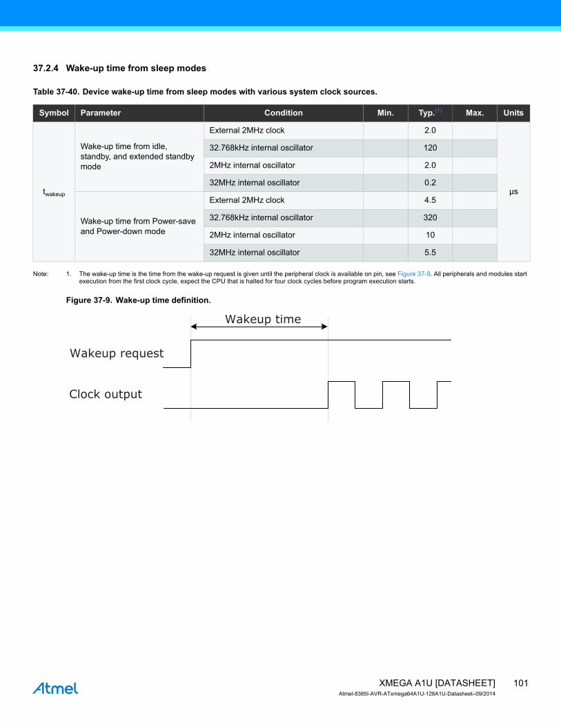
101XMEGA A1U [DATASHEET]Atmel-8385I-AVR-ATxmega64A1U-128A1U-Datasheet–09/2014
37.2.4 Wake-up time from sleep modes
Table 37-40. Device wake-up time from sleep modes with various system clock sources.
Note: 1. The wake-up time is the time from the wake-up request is given until the peripheral clock is available on pin, see Figure 37-9. All peripherals and modules start execution from the first clock cycle, expect the CPU that is halted for four clock cycles before program execution starts.
Figure 37-9. Wake-up time definition.
Symbol Parameter Condition Min. Typ.(1) Max. Units
twakeup
Wake-up time from idle, standby, and extended standby mode
External 2MHz clock 2.0
µs
32.768kHz internal oscillator 120
2MHz internal oscillator 2.0
32MHz internal oscillator 0.2
Wake-up time from Power-save and Power-down mode
External 2MHz clock 4.5
32.768kHz internal oscillator 320
2MHz internal oscillator 10
32MHz internal oscillator 5.5
Wakeup request
Clock output
Wakeup time
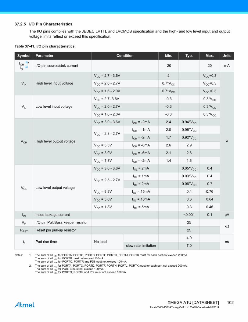
102XMEGA A1U [DATASHEET]Atmel-8385I-AVR-ATxmega64A1U-128A1U-Datasheet–09/2014
37.2.5 I/O Pin Characteristics
The I/O pins complies with the JEDEC LVTTL and LVCMOS specification and the high- and low level input and output voltage limits reflect or exceed this specification.
Table 37-41. I/O pin characteristics.
Notes: 1. The sum of all IOH for PORTA, PORTC, PORTD, PORTF, PORTH, PORTJ, PORTK must for each port not exceed 200mA.The sum of all IOH for PORTB must not exceed 100mA.The sum of all IOH for PORTQ, PORTR and PDI must not exceed 100mA.
2. The sum of all IOL for PORTA, PORTC, PORTD, PORTF, PORTH, PORTJ, PORTK must for each port not exceed 200mA.The sum of all IOL for PORTB must not exceed 100mA.The sum of all IOL for PORTQ, PORTR and PDI must not exceed 100mA.
Symbol Parameter Condition Min. Typ. Max. Units
IOH (1)/
IOL (2) I/O pin source/sink current -20 20 mA
VIH High level input voltage
VCC = 2.7 - 3.6V 2 VCC+0.3
V
VCC = 2.0 - 2.7V 0.7*VCC VCC+0.3
VCC = 1.6 - 2.0V 0.7*VCC VCC+0.3
VIL Low level input voltage
VCC = 2.7- 3.6V -0.3 0.3*VCC
VCC = 2.0 - 2.7V -0.3 0.3*VCC
VCC = 1.6 - 2.0V -0.3 0.3*VCC
VOH High level output voltage
VCC = 3.0 - 3.6V IOH = -2mA 2.4 0.94*VCC
VCC = 2.3 - 2.7VIOH = -1mA 2.0 0.96*VCC
IOH = -2mA 1.7 0.92*VCC
VCC = 3.3V IOH = -8mA 2.6 2.9
VCC = 3.0V IOH = -6mA 2.1 2.6
VCC = 1.8V IOH = -2mA 1.4 1.6
VOL Low level output voltage
VCC = 3.0 - 3.6V IOL = 2mA 0.05*VCC 0.4
VCC = 2.3 - 2.7VIOL = 1mA 0.03*VCC 0.4
IOL = 2mA 0.06*VCC 0.7
VCC = 3.3V IOL = 15mA 0.4 0.76
VCC = 3.0V IOL = 10mA 0.3 0.64
VCC = 1.8V IOL = 5mA 0.3 0.46
IIN Input leakage current <0.001 0.1 µA
RP I/O pin Pull/Buss keeper resistor 25kΩ
RRST Reset pin pull-up resistor 25
tr Pad rise time No load4.0
nsslew rate limitation 7.0
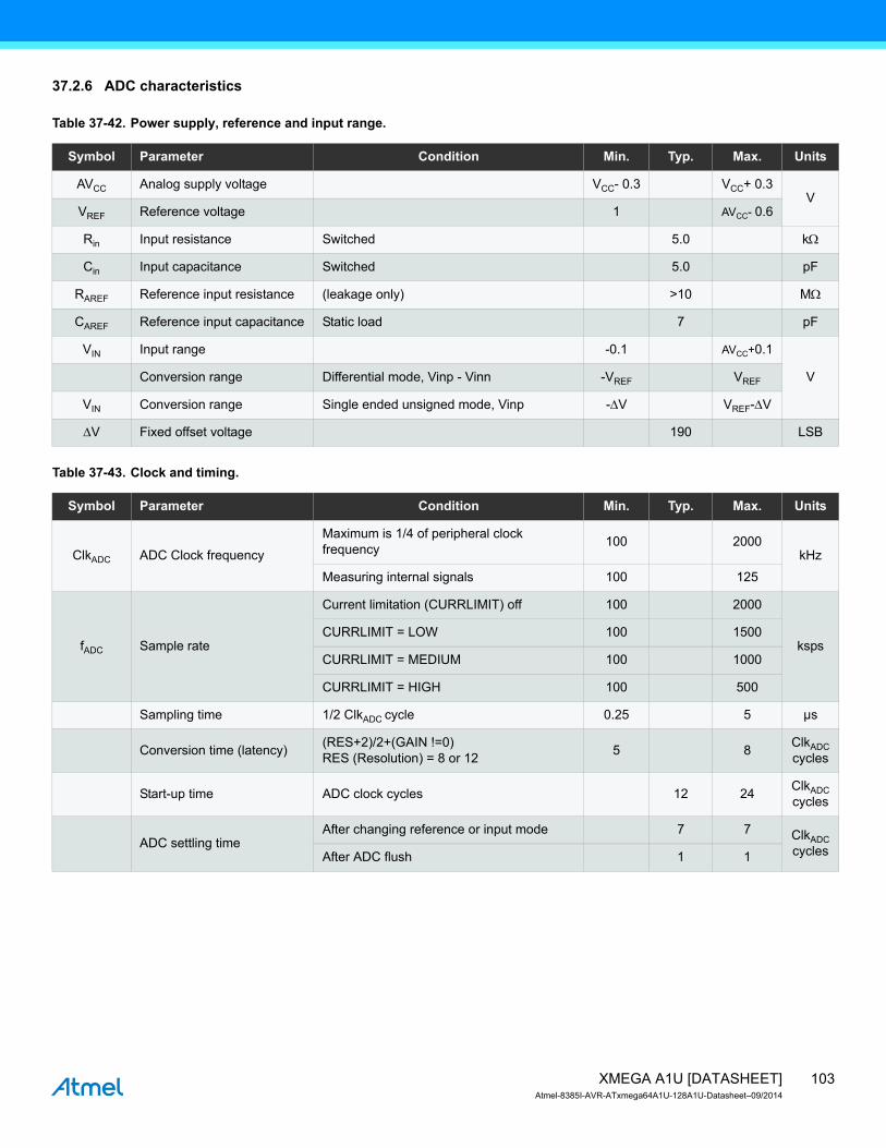
103XMEGA A1U [DATASHEET]Atmel-8385I-AVR-ATxmega64A1U-128A1U-Datasheet–09/2014
37.2.6 ADC characteristics
Table 37-42. Power supply, reference and input range.
Table 37-43. Clock and timing.
Symbol Parameter Condition Min. Typ. Max. Units
AVCC Analog supply voltage VCC- 0.3 VCC+ 0.3V
VREF Reference voltage 1 AVCC- 0.6
Rin Input resistance Switched 5.0 kΩ
Cin Input capacitance Switched 5.0 pF
RAREF Reference input resistance (leakage only) >10 MΩ
CAREF Reference input capacitance Static load 7 pF
VIN Input range -0.1 AVCC+0.1
VConversion range Differential mode, Vinp - Vinn -VREF VREF
VIN Conversion range Single ended unsigned mode, Vinp -ΔV VREF-ΔV
ΔV Fixed offset voltage 190 LSB
Symbol Parameter Condition Min. Typ. Max. Units
ClkADC ADC Clock frequency
Maximum is 1/4 of peripheral clock frequency 100 2000
kHz
Measuring internal signals 100 125
fADC Sample rate
Current limitation (CURRLIMIT) off 100 2000
kspsCURRLIMIT = LOW 100 1500
CURRLIMIT = MEDIUM 100 1000
CURRLIMIT = HIGH 100 500
Sampling time 1/2 ClkADC cycle 0.25 5 µs
Conversion time (latency) (RES+2)/2+(GAIN !=0)RES (Resolution) = 8 or 12 5 8 ClkADC
cycles
Start-up time ADC clock cycles 12 24 ClkADCcycles
ADC settling timeAfter changing reference or input mode 7 7 ClkADC
cyclesAfter ADC flush 1 1
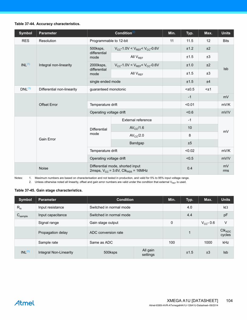
104XMEGA A1U [DATASHEET]Atmel-8385I-AVR-ATxmega64A1U-128A1U-Datasheet–09/2014
Table 37-44. Accuracy characteristics.
Notes: 1. Maximum numbers are based on characterisation and not tested in production, and valid for 5% to 95% input voltage range.2. Unless otherwise noted all linearity, offset and gain error numbers are valid under the condition that external VREF is used.
Table 37-45. Gain stage characteristics.
Symbol Parameter Condition(2) Min. Typ. Max. Units
RES Resolution Programmable to 12-bit 11 11.5 12 Bits
INL(1) Integral non-linearity
500ksps, differential mode
VCC-1.0V < VREF< VCC-0.6V ±1.2 ±2
lsb
All VREF ±1.5 ±3
2000ksps, differential mode
VCC-1.0V < VREF< VCC-0.6V ±1.0 ±2
All VREF ±1.5 ±3
single ended mode ±1.5 ±4
DNL(1) Differential non-linearity guaranteed monotonic <±0.5 <±1
Offset Error
-1 mV
Temperature drift <0.01 mV/K
Operating voltage drift <0.6 mV/V
Gain Error
Differential mode
External reference -1
mVAVCC/1.6 10
AVCC/2.0 8
Bandgap ±5
Temperature drift <0.02 mV/K
Operating voltage drift <0.5 mV/V
Noise Differential mode, shorted input2msps, VCC = 3.6V, ClkPER = 16MHz 0.4 mV
rms
Symbol Parameter Condition Min. Typ. Max. Units
Rin Input resistance Switched in normal mode 4.0 kΩ
Csample Input capacitance Switched in normal mode 4.4 pF
Signal range Gain stage output 0 VCC- 0.6 V
Propagation delay ADC conversion rate 1 ClkADCcycles
Sample rate Same as ADC 100 1000 kHz
INL(1) Integral Non-Linearity 500ksps All gain settings ±1.5 ±3 lsb
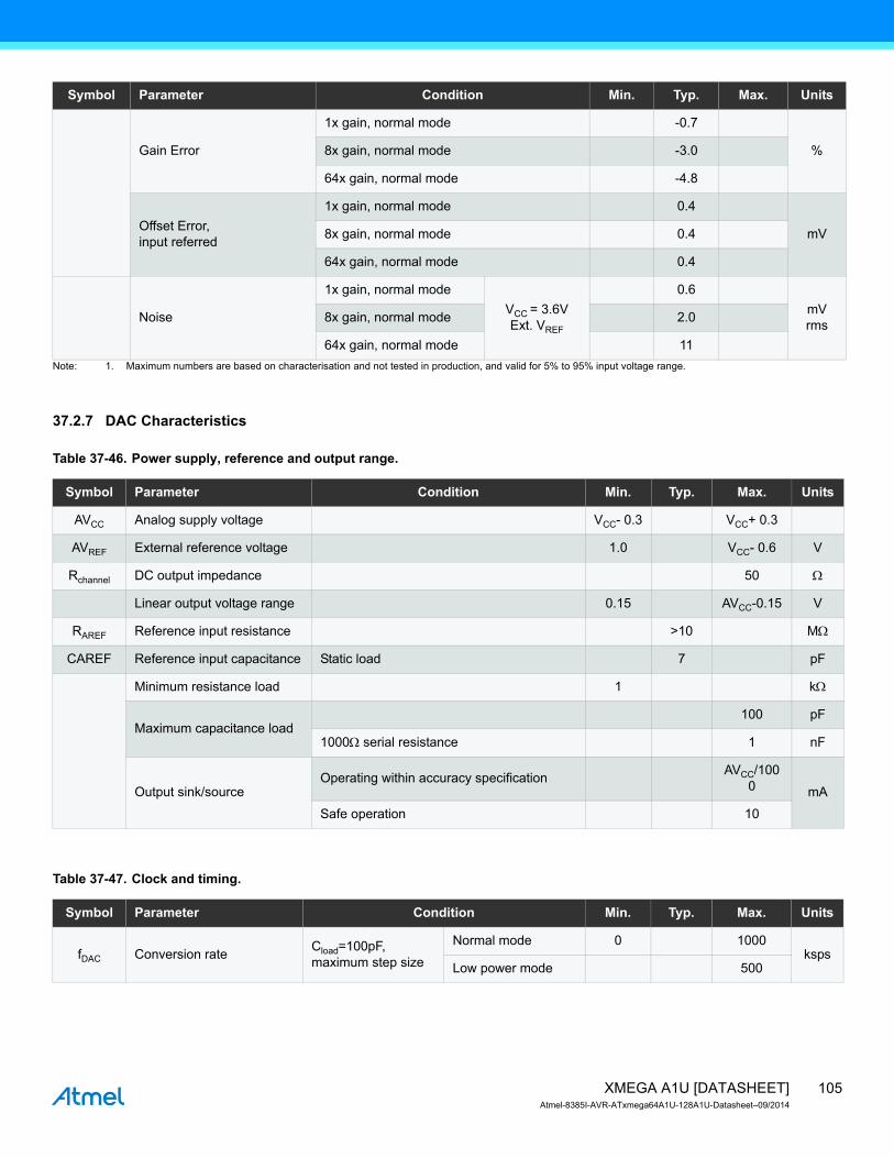
105XMEGA A1U [DATASHEET]Atmel-8385I-AVR-ATxmega64A1U-128A1U-Datasheet–09/2014
Note: 1. Maximum numbers are based on characterisation and not tested in production, and valid for 5% to 95% input voltage range.
37.2.7 DAC Characteristics
Table 37-46. Power supply, reference and output range.
Table 37-47. Clock and timing.
Gain Error
1x gain, normal mode -0.7
%8x gain, normal mode -3.0
64x gain, normal mode -4.8
Offset Error,input referred
1x gain, normal mode 0.4
mV8x gain, normal mode 0.4
64x gain, normal mode 0.4
Noise
1x gain, normal modeVCC = 3.6VExt. VREF
0.6mVrms8x gain, normal mode 2.0
64x gain, normal mode 11
Symbol Parameter Condition Min. Typ. Max. Units
Symbol Parameter Condition Min. Typ. Max. Units
AVCC Analog supply voltage VCC- 0.3 VCC+ 0.3
AVREF External reference voltage 1.0 VCC- 0.6 V
Rchannel DC output impedance 50 Ω
Linear output voltage range 0.15 AVCC-0.15 V
RAREF Reference input resistance >10 MΩ
CAREF Reference input capacitance Static load 7 pF
Minimum resistance load 1 kΩ
Maximum capacitance load100 pF
1000Ω serial resistance 1 nF
Output sink/sourceOperating within accuracy specification AVCC/100
0 mA
Safe operation 10
Symbol Parameter Condition Min. Typ. Max. Units
fDAC Conversion rate Cload=100pF, maximum step size
Normal mode 0 1000ksps
Low power mode 500
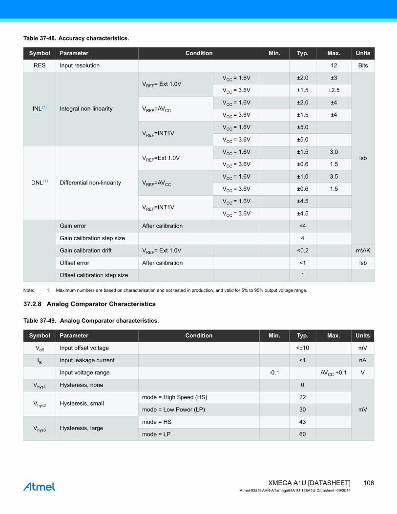
106XMEGA A1U [DATASHEET]Atmel-8385I-AVR-ATxmega64A1U-128A1U-Datasheet–09/2014
Table 37-48. Accuracy characteristics.
Note: 1. Maximum numbers are based on characterisation and not tested in production, and valid for 5% to 95% output voltage range.
37.2.8 Analog Comparator Characteristics
Table 37-49. Analog Comparator characteristics.
Symbol Parameter Condition Min. Typ. Max. Units
RES Input resolution 12 Bits
INL(1) Integral non-linearity
VREF= Ext 1.0VVCC = 1.6V ±2.0 ±3
lsb
VCC = 3.6V ±1.5 ±2.5
VREF=AVCC
VCC = 1.6V ±2.0 ±4
VCC = 3.6V ±1.5 ±4
VREF=INT1VVCC = 1.6V ±5.0
VCC = 3.6V ±5.0
DNL(1) Differential non-linearity
VREF=Ext 1.0VVCC = 1.6V ±1.5 3.0
VCC = 3.6V ±0.6 1.5
VREF=AVCC
VCC = 1.6V ±1.0 3.5
VCC = 3.6V ±0.6 1.5
VREF=INT1VVCC = 1.6V ±4.5
VCC = 3.6V ±4.5
Gain error After calibration <4
Gain calibration step size 4
Gain calibration drift VREF= Ext 1.0V <0.2 mV/K
Offset error After calibration <1 lsb
Offset calibration step size 1
Symbol Parameter Condition Min. Typ. Max. Units
Voff Input offset voltage <±10 mV
Ilk Input leakage current <1 nA
Input voltage range -0.1 AVCC +0.1 V
Vhys1 Hysteresis, none 0
mVVhys2 Hysteresis, small
mode = High Speed (HS) 22
mode = Low Power (LP) 30
Vhys3 Hysteresis, largemode = HS 43
mode = LP 60
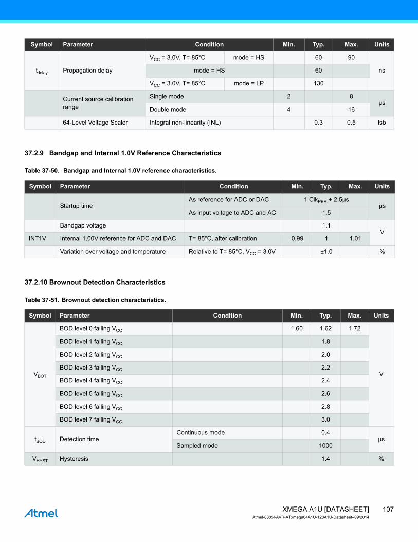
107XMEGA A1U [DATASHEET]Atmel-8385I-AVR-ATxmega64A1U-128A1U-Datasheet–09/2014
37.2.9 Bandgap and Internal 1.0V Reference Characteristics
Table 37-50. Bandgap and Internal 1.0V reference characteristics.
37.2.10 Brownout Detection Characteristics
Table 37-51. Brownout detection characteristics.
tdelay Propagation delay
VCC = 3.0V, T= 85°C mode = HS 60 90
nsmode = HS 60
VCC = 3.0V, T= 85°C mode = LP 130
Current source calibration range
Single mode 2 8µs
Double mode 4 16
64-Level Voltage Scaler Integral non-linearity (INL) 0.3 0.5 lsb
Symbol Parameter Condition Min. Typ. Max. Units
Symbol Parameter Condition Min. Typ. Max. Units
Startup timeAs reference for ADC or DAC 1 ClkPER + 2.5µs
µsAs input voltage to ADC and AC 1.5
Bandgap voltage 1.1V
INT1V Internal 1.00V reference for ADC and DAC T= 85°C, after calibration 0.99 1 1.01
Variation over voltage and temperature Relative to T= 85°C, VCC = 3.0V ±1.0 %
Symbol Parameter Condition Min. Typ. Max. Units
VBOT
BOD level 0 falling VCC 1.60 1.62 1.72
V
BOD level 1 falling VCC 1.8
BOD level 2 falling VCC 2.0
BOD level 3 falling VCC 2.2
BOD level 4 falling VCC 2.4
BOD level 5 falling VCC 2.6
BOD level 6 falling VCC 2.8
BOD level 7 falling VCC 3.0
tBOD Detection timeContinuous mode 0.4
µsSampled mode 1000
VHYST Hysteresis 1.4 %
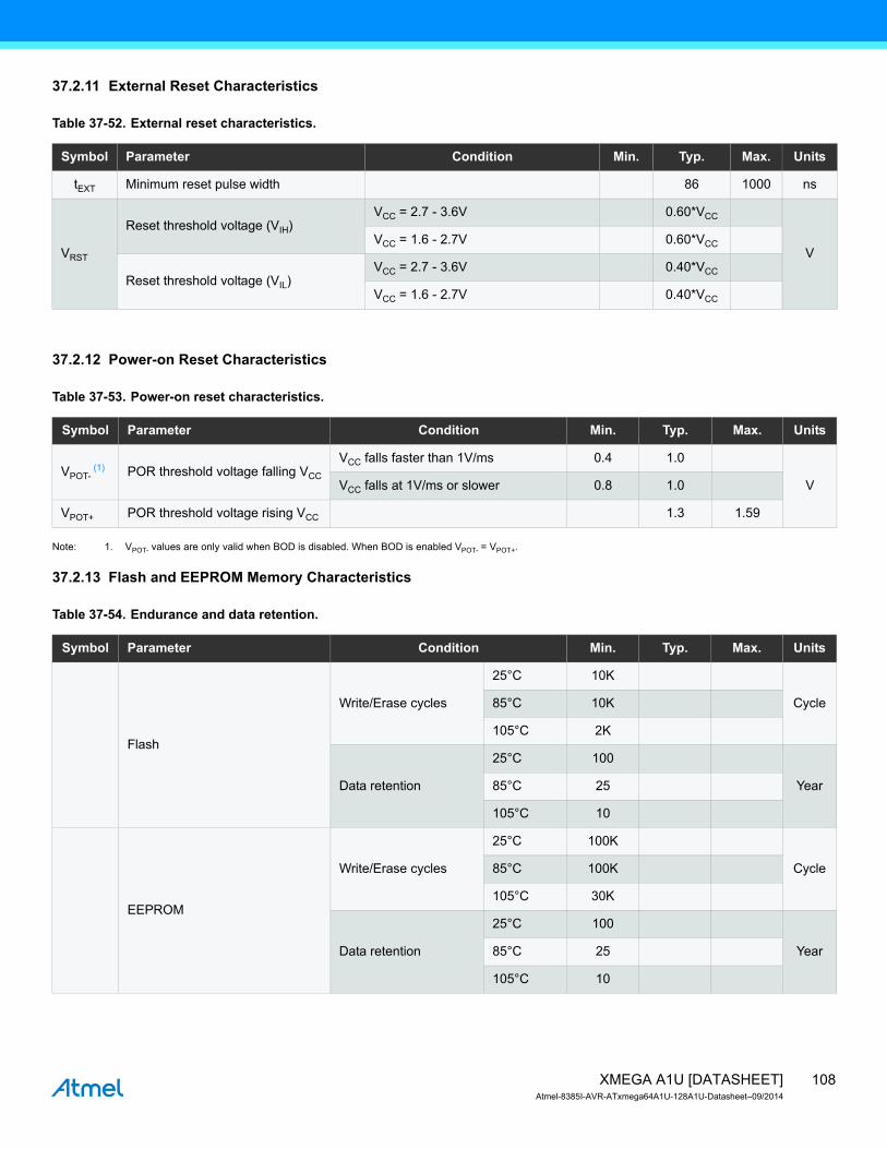
108XMEGA A1U [DATASHEET]Atmel-8385I-AVR-ATxmega64A1U-128A1U-Datasheet–09/2014
37.2.11 External Reset Characteristics
Table 37-52. External reset characteristics.
37.2.12 Power-on Reset Characteristics
Table 37-53. Power-on reset characteristics.
Note: 1. VPOT- values are only valid when BOD is disabled. When BOD is enabled VPOT- = VPOT+.
37.2.13 Flash and EEPROM Memory Characteristics
Table 37-54. Endurance and data retention.
Symbol Parameter Condition Min. Typ. Max. Units
tEXT Minimum reset pulse width 86 1000 ns
VRST
Reset threshold voltage (VIH)VCC = 2.7 - 3.6V 0.60*VCC
VVCC = 1.6 - 2.7V 0.60*VCC
Reset threshold voltage (VIL)VCC = 2.7 - 3.6V 0.40*VCC
VCC = 1.6 - 2.7V 0.40*VCC
Symbol Parameter Condition Min. Typ. Max. Units
VPOT- (1) POR threshold voltage falling VCC
VCC falls faster than 1V/ms 0.4 1.0
VVCC falls at 1V/ms or slower 0.8 1.0
VPOT+ POR threshold voltage rising VCC 1.3 1.59
Symbol Parameter Condition Min. Typ. Max. Units
Flash
Write/Erase cycles
25°C 10K
Cycle85°C 10K
105°C 2K
Data retention
25°C 100
Year85°C 25
105°C 10
EEPROM
Write/Erase cycles
25°C 100K
Cycle85°C 100K
105°C 30K
Data retention
25°C 100
Year85°C 25
105°C 10
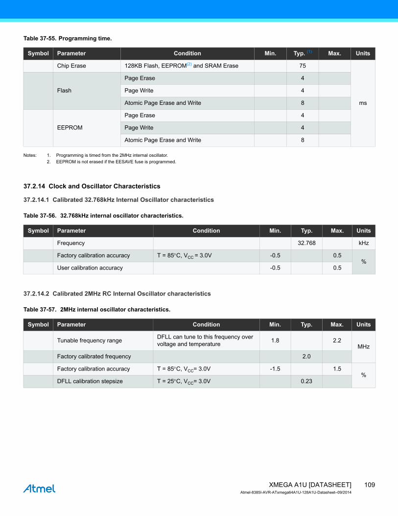
109XMEGA A1U [DATASHEET]Atmel-8385I-AVR-ATxmega64A1U-128A1U-Datasheet–09/2014
Table 37-55. Programming time.
Notes: 1. Programming is timed from the 2MHz internal oscillator.2. EEPROM is not erased if the EESAVE fuse is programmed.
37.2.14 Clock and Oscillator Characteristics
37.2.14.1 Calibrated 32.768kHz Internal Oscillator characteristics
Table 37-56. 32.768kHz internal oscillator characteristics.
37.2.14.2 Calibrated 2MHz RC Internal Oscillator characteristics
Table 37-57. 2MHz internal oscillator characteristics.
Symbol Parameter Condition Min. Typ. (1) Max. Units
Chip Erase 128KB Flash, EEPROM(2) and SRAM Erase 75
ms
Flash
Page Erase 4
Page Write 4
Atomic Page Erase and Write 8
EEPROM
Page Erase 4
Page Write 4
Atomic Page Erase and Write 8
Symbol Parameter Condition Min. Typ. Max. Units
Frequency 32.768 kHz
Factory calibration accuracy T = 85°C, VCC = 3.0V -0.5 0.5%
User calibration accuracy -0.5 0.5
Symbol Parameter Condition Min. Typ. Max. Units
Tunable frequency range DFLL can tune to this frequency over voltage and temperature 1.8 2.2
MHz
Factory calibrated frequency 2.0
Factory calibration accuracy T = 85°C, VCC= 3.0V -1.5 1.5%
DFLL calibration stepsize T = 25°C, VCC= 3.0V 0.23
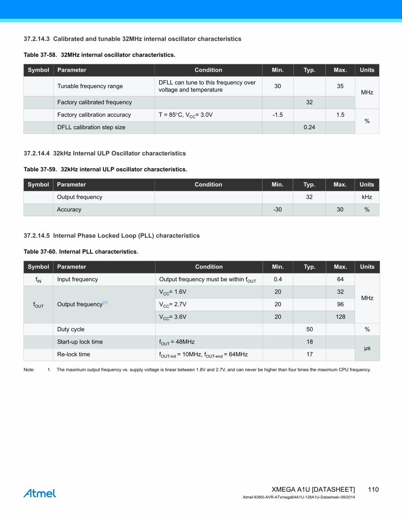
110XMEGA A1U [DATASHEET]Atmel-8385I-AVR-ATxmega64A1U-128A1U-Datasheet–09/2014
37.2.14.3 Calibrated and tunable 32MHz internal oscillator characteristics
Table 37-58. 32MHz internal oscillator characteristics.
37.2.14.4 32kHz Internal ULP Oscillator characteristics
Table 37-59. 32kHz internal ULP oscillator characteristics.
37.2.14.5 Internal Phase Locked Loop (PLL) characteristics
Table 37-60. Internal PLL characteristics.
Note: 1. The maximum output frequency vs. supply voltage is linear between 1.8V and 2.7V, and can never be higher than four times the maximum CPU frequency.
Symbol Parameter Condition Min. Typ. Max. Units
Tunable frequency range DFLL can tune to this frequency over voltage and temperature 30 35
MHz
Factory calibrated frequency 32
Factory calibration accuracy T = 85°C, VCC= 3.0V -1.5 1.5%
DFLL calibration step size 0.24
Symbol Parameter Condition Min. Typ. Max. Units
Output frequency 32 kHz
Accuracy -30 30 %
Symbol Parameter Condition Min. Typ. Max. Units
fIN Input frequency Output frequency must be within fOUT 0.4 64
MHzfOUT Output frequency(1)
VCC= 1.6V 20 32
VCC= 2.7V 20 96
VCC= 3.6V 20 128
Duty cycle 50 %
Start-up lock time fOUT = 48MHz 18µs
Re-lock time fOUT-init = 10MHz, fOUT-end = 64MHz 17
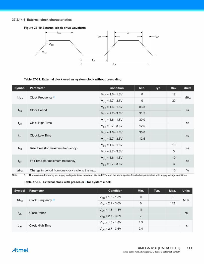
111XMEGA A1U [DATASHEET]Atmel-8385I-AVR-ATxmega64A1U-128A1U-Datasheet–09/2014
37.2.14.6 External clock characteristics
Figure 37-10.External clock drive waveform.
Table 37-61. External clock used as system clock without prescaling.
Note: 1. The maximum frequency vs. supply voltage is linear between 1.6V and 2.7V, and the same applies for all other parameters with supply voltage conditions.
Table 37-62. External clock with prescaler (1)for system clock.
tCH
tCL
tCK
tCH
VIL1
VIH1
tCR tCF
Symbol Parameter Condition Min. Typ. Max. Units
1/tCK Clock Frequency (1)VCC = 1.6 - 1.8V 0 12
MHzVCC = 2.7 - 3.6V 0 32
tCK Clock PeriodVCC = 1.6 - 1.8V 83.3
nsVCC = 2.7 - 3.6V 31.5
tCH Clock High TimeVCC = 1.6 - 1.8V 30.0
nsVCC = 2.7 - 3.6V 12.5
tCL Clock Low TimeVCC = 1.6 - 1.8V 30.0
nsVCC = 2.7 - 3.6V 12.5
tCR Rise Time (for maximum frequency)VCC = 1.6 - 1.8V 10
nsVCC = 2.7 - 3.6V 3
tCF Fall Time (for maximum frequency)VCC = 1.6 - 1.8V 10
nsVCC = 2.7 - 3.6V 3
ΔtCK Change in period from one clock cycle to the next 10 %
Symbol Parameter Condition Min. Typ. Max. Units
1/tCK Clock Frequency (2)VCC = 1.6 - 1.8V 0 90
MHzVCC = 2.7 - 3.6V 0 142
tCK Clock PeriodVCC = 1.6 - 1.8V 11
nsVCC = 2.7 - 3.6V 7
tCH Clock High TimeVCC = 1.6 - 1.8V 4.5
nsVCC = 2.7 - 3.6V 2.4
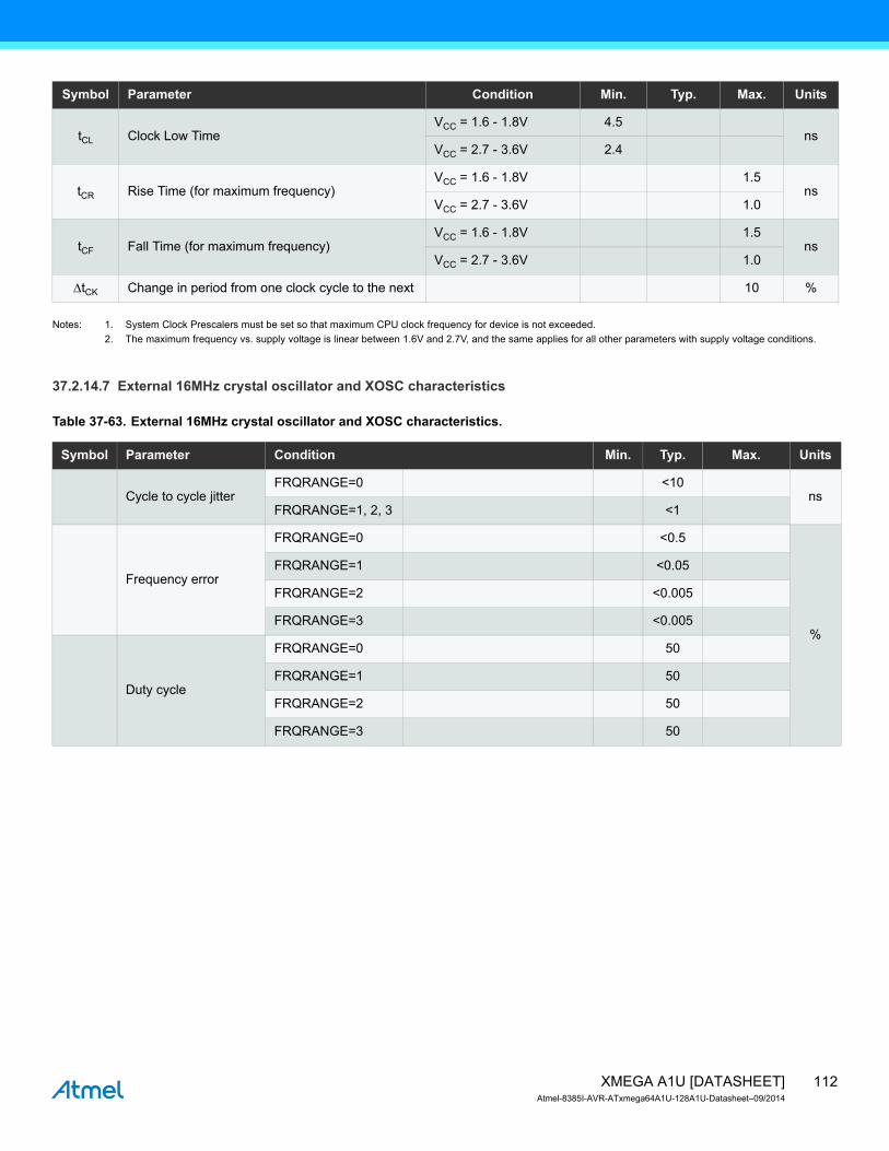
112XMEGA A1U [DATASHEET]Atmel-8385I-AVR-ATxmega64A1U-128A1U-Datasheet–09/2014
Notes: 1. System Clock Prescalers must be set so that maximum CPU clock frequency for device is not exceeded.2. The maximum frequency vs. supply voltage is linear between 1.6V and 2.7V, and the same applies for all other parameters with supply voltage conditions.
37.2.14.7 External 16MHz crystal oscillator and XOSC characteristics
Table 37-63. External 16MHz crystal oscillator and XOSC characteristics..
tCL Clock Low TimeVCC = 1.6 - 1.8V 4.5
nsVCC = 2.7 - 3.6V 2.4
tCR Rise Time (for maximum frequency)VCC = 1.6 - 1.8V 1.5
nsVCC = 2.7 - 3.6V 1.0
tCF Fall Time (for maximum frequency)VCC = 1.6 - 1.8V 1.5
nsVCC = 2.7 - 3.6V 1.0
ΔtCK Change in period from one clock cycle to the next 10 %
Symbol Parameter Condition Min. Typ. Max. Units
Symbol Parameter Condition Min. Typ. Max. Units
Cycle to cycle jitterFRQRANGE=0 <10
nsFRQRANGE=1, 2, 3 <1
Frequency error
FRQRANGE=0 <0.5
%
FRQRANGE=1 <0.05
FRQRANGE=2 <0.005
FRQRANGE=3 <0.005
Duty cycle
FRQRANGE=0 50
FRQRANGE=1 50
FRQRANGE=2 50
FRQRANGE=3 50
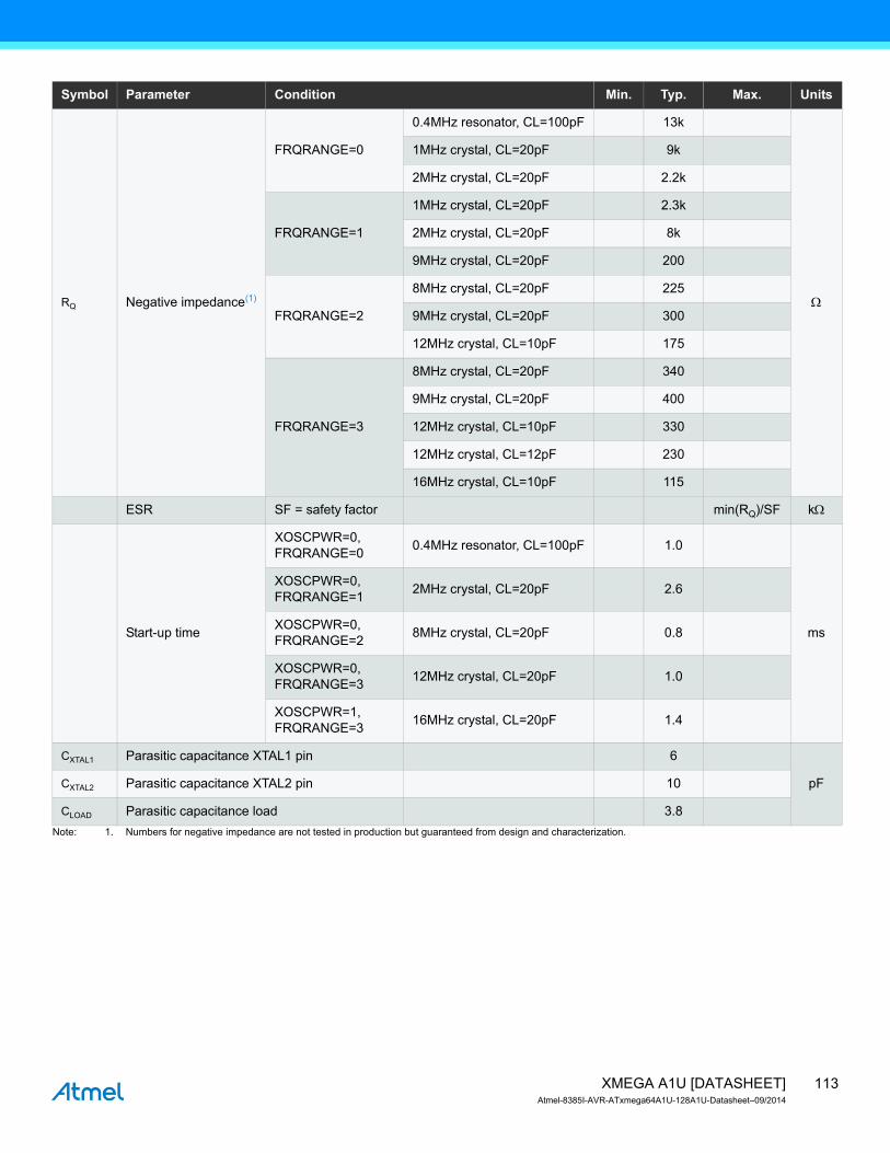
113XMEGA A1U [DATASHEET]Atmel-8385I-AVR-ATxmega64A1U-128A1U-Datasheet–09/2014
Note: 1. Numbers for negative impedance are not tested in production but guaranteed from design and characterization.
RQ Negative impedance(1)
FRQRANGE=0
0.4MHz resonator, CL=100pF 13k
Ω
1MHz crystal, CL=20pF 9k
2MHz crystal, CL=20pF 2.2k
FRQRANGE=1
1MHz crystal, CL=20pF 2.3k
2MHz crystal, CL=20pF 8k
9MHz crystal, CL=20pF 200
FRQRANGE=2
8MHz crystal, CL=20pF 225
9MHz crystal, CL=20pF 300
12MHz crystal, CL=10pF 175
FRQRANGE=3
8MHz crystal, CL=20pF 340
9MHz crystal, CL=20pF 400
12MHz crystal, CL=10pF 330
12MHz crystal, CL=12pF 230
16MHz crystal, CL=10pF 115
ESR SF = safety factor min(RQ)/SF kΩ
Start-up time
XOSCPWR=0,FRQRANGE=0 0.4MHz resonator, CL=100pF 1.0
ms
XOSCPWR=0,FRQRANGE=1 2MHz crystal, CL=20pF 2.6
XOSCPWR=0,FRQRANGE=2 8MHz crystal, CL=20pF 0.8
XOSCPWR=0,FRQRANGE=3 12MHz crystal, CL=20pF 1.0
XOSCPWR=1,FRQRANGE=3 16MHz crystal, CL=20pF 1.4
CXTAL1 Parasitic capacitance XTAL1 pin 6
pFCXTAL2 Parasitic capacitance XTAL2 pin 10
CLOAD Parasitic capacitance load 3.8
Symbol Parameter Condition Min. Typ. Max. Units
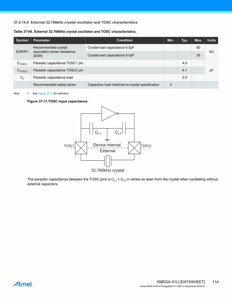
114XMEGA A1U [DATASHEET]Atmel-8385I-AVR-ATxmega64A1U-128A1U-Datasheet–09/2014
37.2.14.8 External 32.768kHz crystal oscillator and TOSC characteristics
Table 37-64. External 32.768kHz crystal oscillator and TOSC characteristics.
Note: 1. See Figure 37-11 for definition.
Figure 37-11.TOSC input capacitance.
The parasitic capacitance between the TOSC pins is CL1 + CL2 in series as seen from the crystal when oscillating without external capacitors.
Symbol Parameter Condition Min. Typ. Max. Units
ESR/R1Recommended crystal equivalent series resistance (ESR)
Crystal load capacitance 6.5pF 60kΩ
Crystal load capacitance 9.0pF 35
CTOSC1 Parasitic capacitance TOSC1 pin 4.0
pFCTOSC2 Parasitic capacitance TOSC2 pin 4.1
CL Parasitic capacitance load 2.0
Recommended safety factor Capacitive load matched to crystal specification 3
CL1 CL2
2CSOT1CSOT Device internalExternal
32.768kHz crystal

115XMEGA A1U [DATASHEET]Atmel-8385I-AVR-ATxmega64A1U-128A1U-Datasheet–09/2014
37.2.15 SPI Characteristics
Figure 37-12.SPI timing requirements in master mode.
Figure 37-13.SPI timing requirements in slave mode.
MSB LSB
BSLBSM
tMOS
tMIS tMIH
tSCKW
tSCK
tMOH tMOH
tSCKFtSCKR
tSCKW
MOSI(Data Output)
MISO(Data Input)
SCK(CPOL = 1)
SCK(CPOL = 0)
SS
MSB LSB
BSLBSM
tSIS tSIH
tSSCKW
tSSCKW
tSSCK
tSSH
tSOSSH
tSCKR tSCKF
tSOS
tSSS
tSOSSS
MISO(Data Output)
MOSI(Data Input)
SCK(CPOL = 1)
SCK(CPOL = 0)
SS

116XMEGA A1U [DATASHEET]Atmel-8385I-AVR-ATxmega64A1U-128A1U-Datasheet–09/2014
Table 37-65. SPI timing characteristics and requirements.
Symbol Parameter Condition Min. Typ. Max. Units
tSCK SCK period Master (See Table 21-4 in XMEGA AU Manual)
ns
tSCKW SCK high/low width Master 0.5*SCK
tSCKR SCK rise time Master 2.7
tSCKF SCK fall time Master 2.7
tMIS MISO setup to SCK Master 11
tMIH MISO hold after SCK Master 0
tMOS MOSI setup SCK Master 0.5*SCK
tMOH
MOSI hold after SCK Master 1
SCK to out high Master 1
tSSCK Slave SCK period Slave 4*tClkPER
tSSCKW SCK high/low width Slave 2*tClkPER
tSSCKR SCK rise time Slave 1600
tSSCKF SCK fall time Slave 1600
tSIS MOSI setup to SCK Slave 3
tSIH MOSI hold after SCK Slave tSCK
tSSS SS setup to SCK Slave 20
tSSH SS hold after SCK Slave 20
tSOS MISO setup SCK Slave 8
tSOH MISO hold after SCK Slave 13
tSOSS MISO setup after SS low Slave 11
tSOSH MISO hold after SS high Slave 8

117XMEGA A1U [DATASHEET]Atmel-8385I-AVR-ATxmega64A1U-128A1U-Datasheet–09/2014
37.2.16 EBI characteristics
Table 37-66. EBI SRAM characteristics and requirements.
Symbol Parameter Condition Min. Typ. Max. Units
tClkPER2 SRAM clock period 0.5*tClkPER
tALH SRAM address hold after ALE low tClkPER2
tALS SRAM address setup before ALE low (read and write) tClkPER2
tALW SRAM ALE width tClkPER2
tARH SRAM address hold after RE high tClkPER2
tARS SRAM address setup before RE high tClkPER2
tAWH SRAM address hold after WE high tClkPER2
tAWS SRAM Address setup before WE high tClkPER2
tDRH SRAM data hold after RE high 0
tDRS SRAM data setup to RE high 3.0V 12
tDRS SRAM data setup to RE high 2.7V, 85°C 17
ns
tDRS SRAM data setup to RE high 1.6V, 85°C 27
tDWH SRAM data hold after WE high tClkPER2
tDWS SRAM data setup to WE high tClkPER2
tRW SRAM read enable pulse width tClkPER2*SRWS
tWW SRAM write enable pulse width tClkPER2*SRWS
tCH SRAM chip select hold after RE/WE high tClkPER2
tCRS SRAM chip select setup to RE low or ALE high 0
tCWS SRAM chip select setup to WE low (no ALE) tClkPER2

118XMEGA A1U [DATASHEET]Atmel-8385I-AVR-ATxmega64A1U-128A1U-Datasheet–09/2014
Table 37-67. EBI SDRAM characteristics and requirements.
37.2.17 Two-Wire Interface Characteristics
Table 37-68 on page 119 describes the requirements for devices connected to the Two-Wire Interface Bus. The Atmel AVR XMEGA Two-Wire Interface meets or exceeds these requirements under the noted conditions. Timing symbols refer to Figure 37-14.
Figure 37-14.Two-Wire Interface bus timing.
Symbol Parameter Condition Min. Typ. Max. Units
tClkPER2 SDRAM clock period 0.5*tClkPER
ns
tAH SDRAM address hold time 0.5*tClkPER2
tAS SDRAM address setup time 0.5*tClkPER2
tCH SDRAM clock high-level width 0.5*tClkPER2
tCL SDRAM clock low-level width 0.5*tClkPER2
tCKH SDRAM CKE hold time 0.5*tClkPER2
tCKS SDRAM CKE setup time 0.5*tClkPER2
tCMH SDRAM CS, RAS, CAS, WE, DQM hold time 0.5*tClkPER2
tCMS SDRAM CS, RAS, CAS, WE, DQM setup time 0.5*tClkPER2
tDRH SDRAM data in hold after CLK high 0
tAC SDRAM access time from CLK tClkPER-5
tDWH SDRAM data out hold after CLK high 0.5*tClkPER2
tDWS SDRAM data out setup before CLK high 0.5*tClkPER2
tHD;STA
tof
SDA
SCL
tLOWtHIGH
tSU;STA
tBUF
tr
tHD;DAT tSU;DATtSU;STO
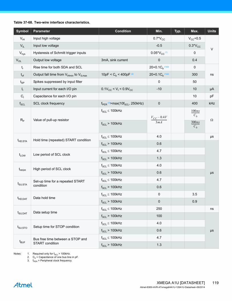
119XMEGA A1U [DATASHEET]Atmel-8385I-AVR-ATxmega64A1U-128A1U-Datasheet–09/2014
Table 37-68. Two-wire interface characteristics.
Notes: 1. Required only for fSCL > 100kHz.2. Cb = Capacitance of one bus line in pF.3. fPER = Peripheral clock frequency.
Symbol Parameter Condition Min. Typ. Max. Units
VIH Input high voltage 0.7*VCC VCC+0.5
VVIL Input low voltage -0.5 0.3*VCC
Vhys Hysteresis of Schmitt trigger inputs 0.05*VCC (1) 0
VOL Output low voltage 3mA, sink current 0 0.4
tr Rise time for both SDA and SCL 20+0.1Cb (1)(2) 0
nstof Output fall time from VIHmin to VILmax 10pF < Cb < 400pF (2) 20+0.1Cb (1)(2) 300
tSP Spikes suppressed by input filter 0 50
II Input current for each I/O pin 0.1VCC < VI < 0.9VCC -10 10 µA
CI Capacitance for each I/O pin 10 pF
fSCL SCL clock frequency fPER (3)>max(10fSCL, 250kHz) 0 400 kHz
RP Value of pull-up resistor
fSCL ≤ 100kHz
ΩfSCL > 100kHz
tHD;STA Hold time (repeated) START conditionfSCL ≤ 100kHz 4.0 µs
fSCL > 100kHz 0.6
µs
tLOW Low period of SCL clockfSCL ≤ 100kHz 4.7
fSCL > 100kHz 1.3
tHIGH High period of SCL clockfSCL ≤ 100kHz 4.0
fSCL > 100kHz 0.6
tSU;STASet-up time for a repeated START condition
fSCL ≤ 100kHz 4.7
fSCL > 100kHz 0.6
tHD;DAT Data hold timefSCL ≤ 100kHz 0 3.5
fSCL > 100kHz 0 0.9
tSU;DAT Data setup timefSCL ≤ 100kHz 250 ns
fSCL > 100kHz 100
µstSU;STO Setup time for STOP condition
fSCL ≤ 100kHz 4.0
fSCL > 100kHz 0.6
tBUFBus free time between a STOP and START condition
fSCL ≤ 100kHz 4.7
fSCL > 100kHz 1.3
VCC 0.4V–3mA
----------------------------
100nsCb---------------
300nsCb---------------
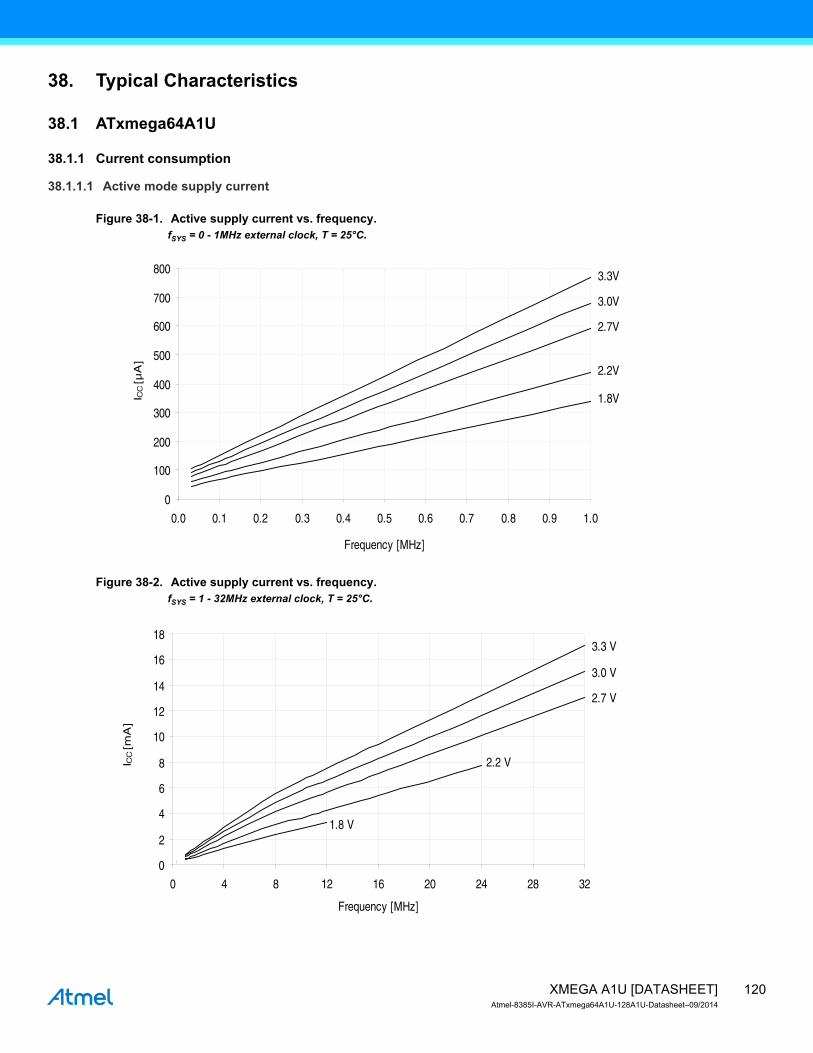
120XMEGA A1U [DATASHEET]Atmel-8385I-AVR-ATxmega64A1U-128A1U-Datasheet–09/2014
38. Typical Characteristics
38.1 ATxmega64A1U
38.1.1 Current consumption
38.1.1.1 Active mode supply current
Figure 38-1. Active supply current vs. frequency.fSYS = 0 - 1MHz external clock, T = 25°C.
Figure 38-2. Active supply current vs. frequency.fSYS = 1 - 32MHz external clock, T = 25°C.
3.3V
3.0V
2.7V
2.2V
1.8V
0
100
200
300
400
500
600
700
800
0.0 0.1 0.2 0.3 0.4 0.5 0.6 0.7 0.8 0.9 1.0
Frequency [MHz]
I CC
[µA
]
3.3 V
3.0 V
2.7 V
1.8 V
0
2
4
6
8
10
12
14
16
18
0 4 8 12 16 20 24 28 32
Frequency [MHz]
I CC
[mA
]
2.2 V
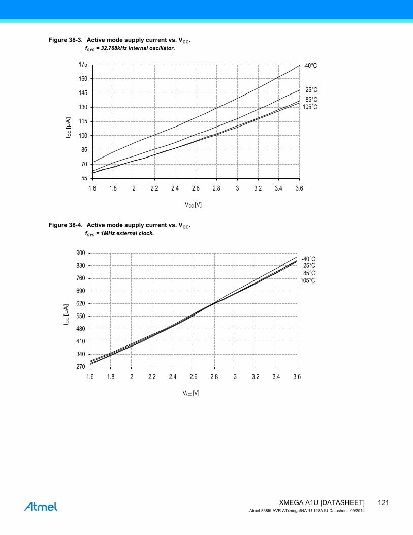
121XMEGA A1U [DATASHEET]Atmel-8385I-AVR-ATxmega64A1U-128A1U-Datasheet–09/2014
Figure 38-3. Active mode supply current vs. VCC.fSYS = 32.768kHz internal oscillator.
Figure 38-4. Active mode supply current vs. VCC.fSYS = 1MHz external clock.
105 °C85 °C25 °C
-40 °C
55
70
85
100
115
130
145
160
175
1.6 1.8 2 2.2 2.4 2.6 2.8 3 3.2 3.4 3.6
I CC
[µA
]
VCC [V]
105 °C85 °C25 °C
-40 °C
270
340
410
480
550
620
690
760
830
900
1.6 1.8 2 2.2 2.4 2.6 2.8 3 3.2 3.4 3.6
I CC
[µA
]
VCC [V]
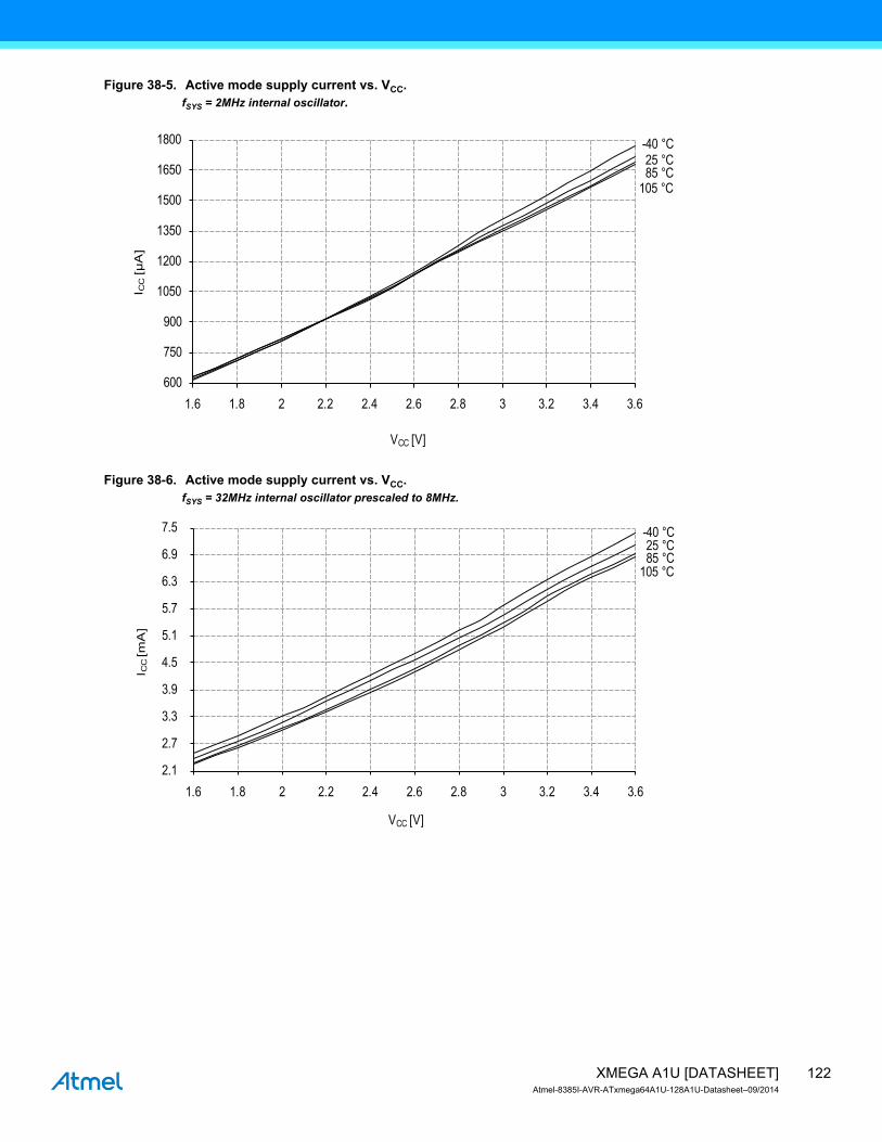
122XMEGA A1U [DATASHEET]Atmel-8385I-AVR-ATxmega64A1U-128A1U-Datasheet–09/2014
Figure 38-5. Active mode supply current vs. VCC.fSYS = 2MHz internal oscillator.
Figure 38-6. Active mode supply current vs. VCC.fSYS = 32MHz internal oscillator prescaled to 8MHz.
105 °C85 °C25 °C
-40 °C
600
750
900
1050
1200
1350
1500
1650
1800
1.6 1.8 2 2.2 2.4 2.6 2.8 3 3.2 3.4 3.6
I CC
[µA
]
VCC [V]
105 °C85 °C25 °C
-40 °C
2.1
2.7
3.3
3.9
4.5
5.1
5.7
6.3
6.9
7.5
1.6 1.8 2 2.2 2.4 2.6 2.8 3 3.2 3.4 3.6
I CC
[mA
]
VCC [V]
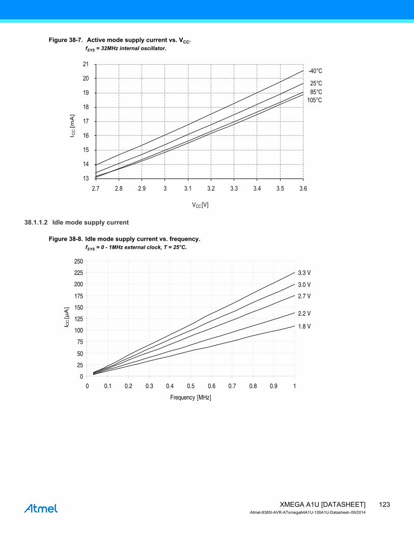
123XMEGA A1U [DATASHEET]Atmel-8385I-AVR-ATxmega64A1U-128A1U-Datasheet–09/2014
Figure 38-7. Active mode supply current vs. VCC.fSYS = 32MHz internal oscillator.
38.1.1.2 Idle mode supply current
Figure 38-8. Idle mode supply current vs. frequency.fSYS = 0 - 1MHz external clock, T = 25°C.
105 °C85 °C25 °C
-40 °C
13
14
15
16
17
18
19
20
21
2.7 2.8 2.9 3 3.1 3.2 3.3 3.4 3.5 3.6
I CC
[mA
]
VCC [V]
3.3 V
3.0 V
2.7 V
2.2 V
1.8 V
0
25
50
75
100
125
150
175
200
225
250
0 0.1 0.2 0.3 0.4 0.5 0.6 0.7 0.8 0.9 1
Frequency [MHz]
I CC
[µA
]
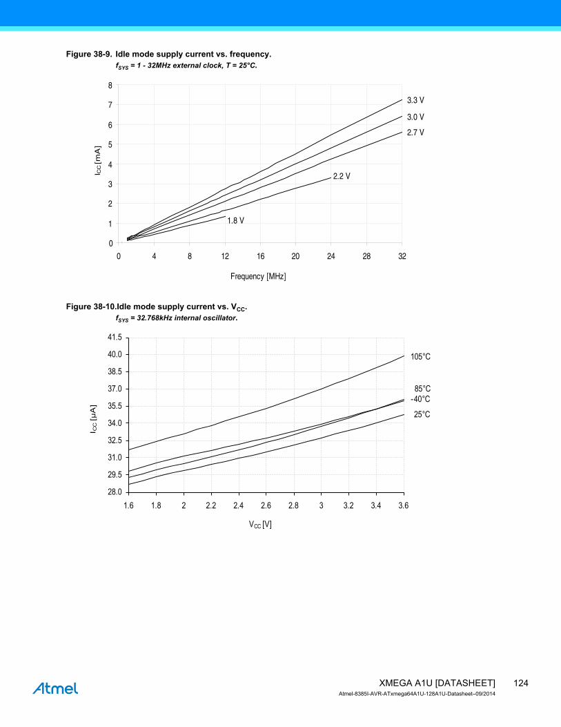
124XMEGA A1U [DATASHEET]Atmel-8385I-AVR-ATxmega64A1U-128A1U-Datasheet–09/2014
Figure 38-9. Idle mode supply current vs. frequency.fSYS = 1 - 32MHz external clock, T = 25°C.
Figure 38-10.Idle mode supply current vs. VCC.fSYS = 32.768kHz internal oscillator.
3.3 V
3.0 V
2.7 V
1.8 V
0
1
2
3
4
5
6
7
8
0 4 8 12 16 20 24 28 32
Frequency [MHz]
I CC
[mA
]
2.2 V
105 °C
85 °C
25 °C
-40 °C
28.0
29.5
31.0
32.5
34.0
35.5
37.0
38.5
40.0
41.5
1.6 1.8 2 2.2 2.4 2.6 2.8 3 3.2 3.4 3.6
I CC
[µA
]
VCC [V]
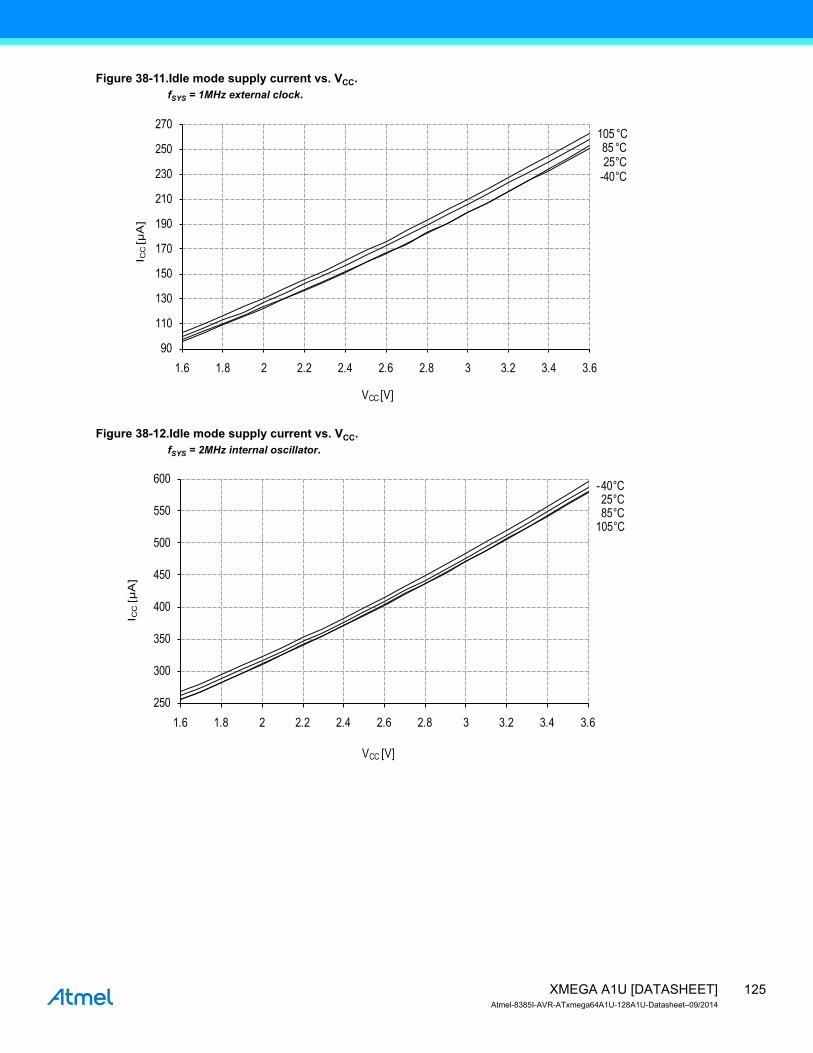
125XMEGA A1U [DATASHEET]Atmel-8385I-AVR-ATxmega64A1U-128A1U-Datasheet–09/2014
Figure 38-11.Idle mode supply current vs. VCC.fSYS = 1MHz external clock.
Figure 38-12.Idle mode supply current vs. VCC.fSYS = 2MHz internal oscillator.
105 °C85 °C25 °C
-40 °C
90
110
130
150
170
190
210
230
250
270
1.6 1.8 2 2.2 2.4 2.6 2.8 3 3.2 3.4 3.6
I CC
[µA
]
VCC [V]
105 °C85 °C25 °C
-40 °C
250
300
350
400
450
500
550
600
1.6 1.8 2 2.2 2.4 2.6 2.8 3 3.2 3.4 3.6
I CC
[µA
]
VCC [V]

126XMEGA A1U [DATASHEET]Atmel-8385I-AVR-ATxmega64A1U-128A1U-Datasheet–09/2014
Figure 38-13.Idle mode supply current vs. VCC.fSYS = 32MHz internal oscillator prescaled to 8MHz.
Figure 38-14.Idle mode current vs. VCC.fSYS = 32MHz internal oscillator.
105 °C85 °C25 °C-40 °C
1000
1300
1600
1900
2200
2500
2800
3100
1.6 1.8 2 2.2 2.4 2.6 2.8 3 3.2 3.4 3.6
I CC
[µA
]
VCC [V]
105 °C85 °C25 °C
-40 °C
5500
5850
6200
6550
6900
7250
7600
7950
8300
8650
2.7 2.8 2.9 3 3.1 3.2 3.3 3.4 3.5 3.6
I CC
[µA
]
VCC [V]

127XMEGA A1U [DATASHEET]Atmel-8385I-AVR-ATxmega64A1U-128A1U-Datasheet–09/2014
38.1.1.3 Power-down mode supply current
Figure 38-15.Power-down mode supply current vs. Temperature.All functions disabled.
Figure 38-16.Power-down mode supply current vs. Temperature.Sampled BOD with Watchdog Timer running on ULP oscillator.
3.3 V3.0 V2.7 V2.2 V1.8 V
0.00
0.75
1.50
2.25
3.00
3.75
4.50
5.25
6.00
-40 -25 -10 5 20 35 50 65 80 95 110
I CC
[µA
]
Temperature [°C]
3.3 V3.0 V2.7 V2.2 V1.8 V
0.80
1.55
2.30
3.05
3.80
4.55
5.30
6.05
-45 -30 -15 0 15 30 45 60 75 90 105
I CC
[µA
]
Temperature [°C]
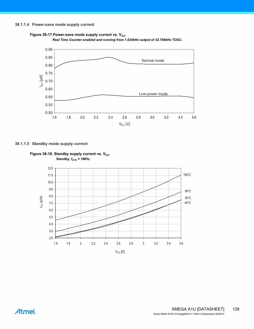
128XMEGA A1U [DATASHEET]Atmel-8385I-AVR-ATxmega64A1U-128A1U-Datasheet–09/2014
38.1.1.4 Power-save mode supply current
Figure 38-17.Power-save mode supply current vs. VCC.Real Time Counter enabled and running from 1.024kHz output of 32.768kHz TOSC.
38.1.1.5 Standby mode supply current
Figure 38-18. Standby supply current vs. VCC.Standby, fSYS = 1MHz.
Normal mode
Low-power mode
0.50
0.55
0.60
0.65
0.70
0.75
0.80
0.85
0.90
VCC [V]
I CC [µ
A]
1.6 1.8 2.0 2.2 2.4 2.6 2.8 3.0 3.2 3.4 3.6
105°C
85°C
25°C-40°C
2.5
3.5
4.5
5.5
6.5
7.5
8.5
9.5
10.5
11.5
12.5
1.6 1.8 2 2.2 2.4 2.6 2.8 3 3.2 3.4 3.6
I CC
[µA
]
VCC [V]
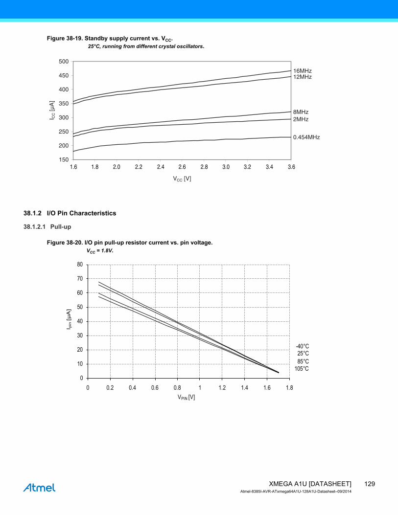
129XMEGA A1U [DATASHEET]Atmel-8385I-AVR-ATxmega64A1U-128A1U-Datasheet–09/2014
Figure 38-19. Standby supply current vs. VCC.25°C, running from different crystal oscillators.
38.1.2 I/O Pin Characteristics
38.1.2.1 Pull-up
Figure 38-20. I/O pin pull-up resistor current vs. pin voltage. VCC = 1.8V.
16MHz12MHz
8MHz2MHz
0.454MHz
150
200
250
300
350
400
450
500
VCC [V]
I CC [µ
A]
1.6 1.8 2.0 2.2 2.4 2.6 2.8 3.0 3.2 3.4 3.6
105 °C85 °C25 °C
-40 °C
0
10
20
30
40
50
60
70
80
0 0.2 0.4 0.6 0.8 1 1.2 1.4 1.6 1.8
I pin
[µA
]
VPIN [V]
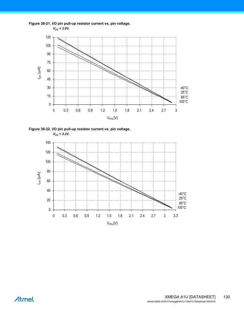
130XMEGA A1U [DATASHEET]Atmel-8385I-AVR-ATxmega64A1U-128A1U-Datasheet–09/2014
Figure 38-21. I/O pin pull-up resistor current vs. pin voltage.VCC = 3.0V.
Figure 38-22. I/O pin pull-up resistor current vs. pin voltage.VCC = 3.3V.
0
15
30
45
60
75
90
105
120
0 0.3 0.6 0.9 1.2 1.5 1.8 2.1 2.4 2.7 3
I pin
[µA
]
VPIN [V]
105 °C85 °C25 °C
-40 °C
0
20
40
60
80
100
120
140
0 0.3 0.6 0.9 1.2 1.5 1.8 2.1 2.4 2.7 3 3.3
I pin
[µA
]
VPIN [V]
105 °C85 °C25 °C
-40 °C
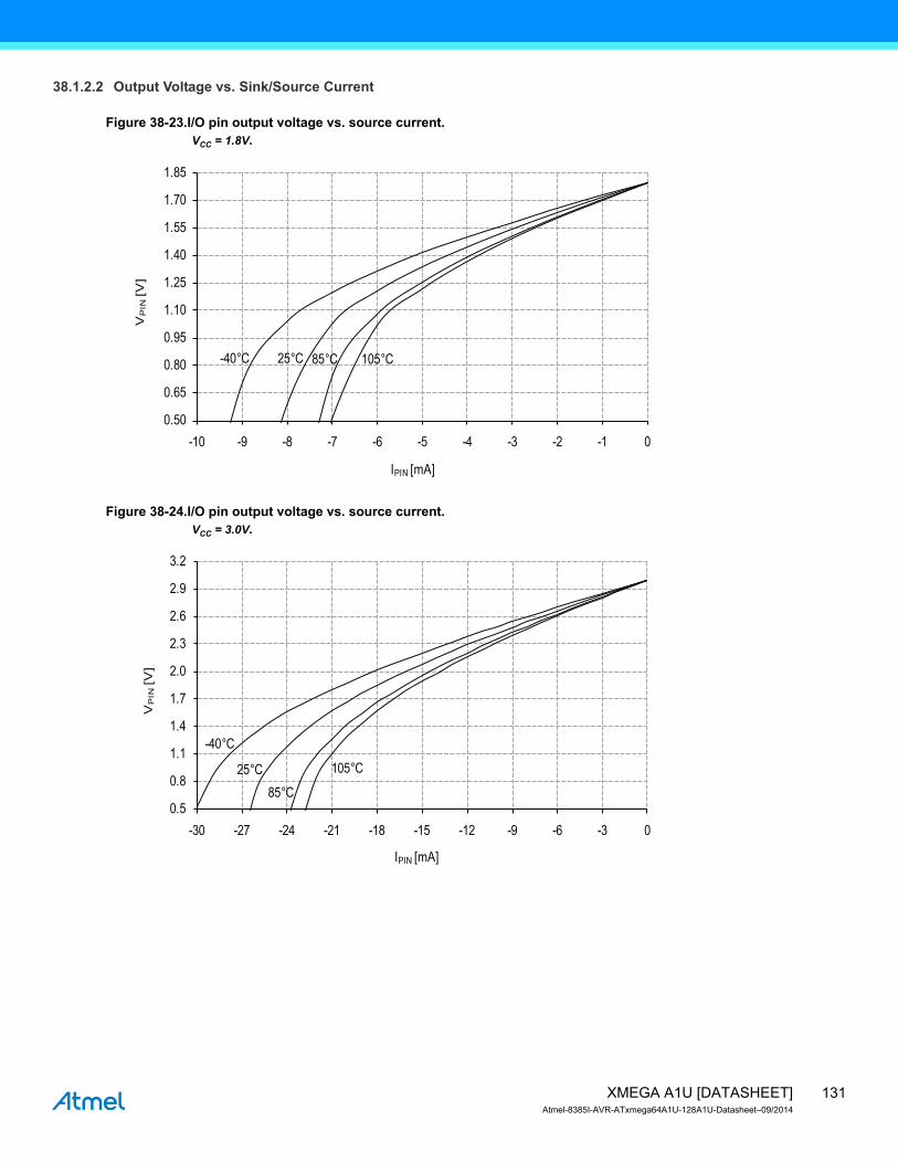
131XMEGA A1U [DATASHEET]Atmel-8385I-AVR-ATxmega64A1U-128A1U-Datasheet–09/2014
38.1.2.2 Output Voltage vs. Sink/Source Current
Figure 38-23.I/O pin output voltage vs. source current.VCC = 1.8V.
Figure 38-24.I/O pin output voltage vs. source current.VCC = 3.0V.
105 °C85 °C25 °C-40°C
0.50
0.65
0.80
0.95
1.10
1.25
1.40
1.55
1.70
1.85
-10 -9 -8 -7 -6 -5 -4 -3 -2 -1 0
VP
IN[V
]
IPIN [mA]
105 °C85 °C
25 °C
-40 °C
0.5
0.8
1.1
1.4
1.7
2.0
2.3
2.6
2.9
3.2
-30 -27 -24 -21 -18 -15 -12 -9 -6 -3 0
VP
IN[V
]
IPIN [mA]
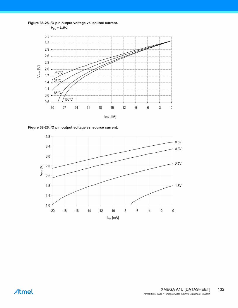
132XMEGA A1U [DATASHEET]Atmel-8385I-AVR-ATxmega64A1U-128A1U-Datasheet–09/2014
Figure 38-25.I/O pin output voltage vs. source current.VCC = 3.3V.
Figure 38-26.I/O pin output voltage vs. source current.
105 °C
85 °C
25 °C
-40 °C
0.5
0.8
1.1
1.4
1.7
2.0
2.3
2.6
2.9
3.2
3.5
-30 -27 -24 -21 -18 -15 -12 -9 -6 -3 0
VP
IN[V
]
IPIN [mA]
3.6V
3.3V
2.7V
1.8V
1.0
1.4
1.8
2.2
2.6
3.0
3.4
3.8
-20 -18 -16 -14 -12 -10 -8 -6 -4 -2 0
IPIN [mA]
VP
IN [
V]

133XMEGA A1U [DATASHEET]Atmel-8385I-AVR-ATxmega64A1U-128A1U-Datasheet–09/2014
Figure 38-27.I/O pin output voltage vs. sink current.VCC = 1.8V.
Figure 38-28.I/O pin output voltage vs. sink current.VCC = 3.0V.
105 °C
85 °C
25 °C-40 °C
0.0
0.2
0.4
0.6
0.8
1.0
1.2
1.4
1.6
0 2 4 6 8 10 12 14 16
VP
IN[V
]
IPIN [mA]
105 °C85 °C25 °C-40 °C
0.00
0.15
0.30
0.45
0.60
0.75
0.90
1.05
1.20
0 3 6 9 12 15 18 21 24 27 30
VP
IN[V
]
IPIN [mA]
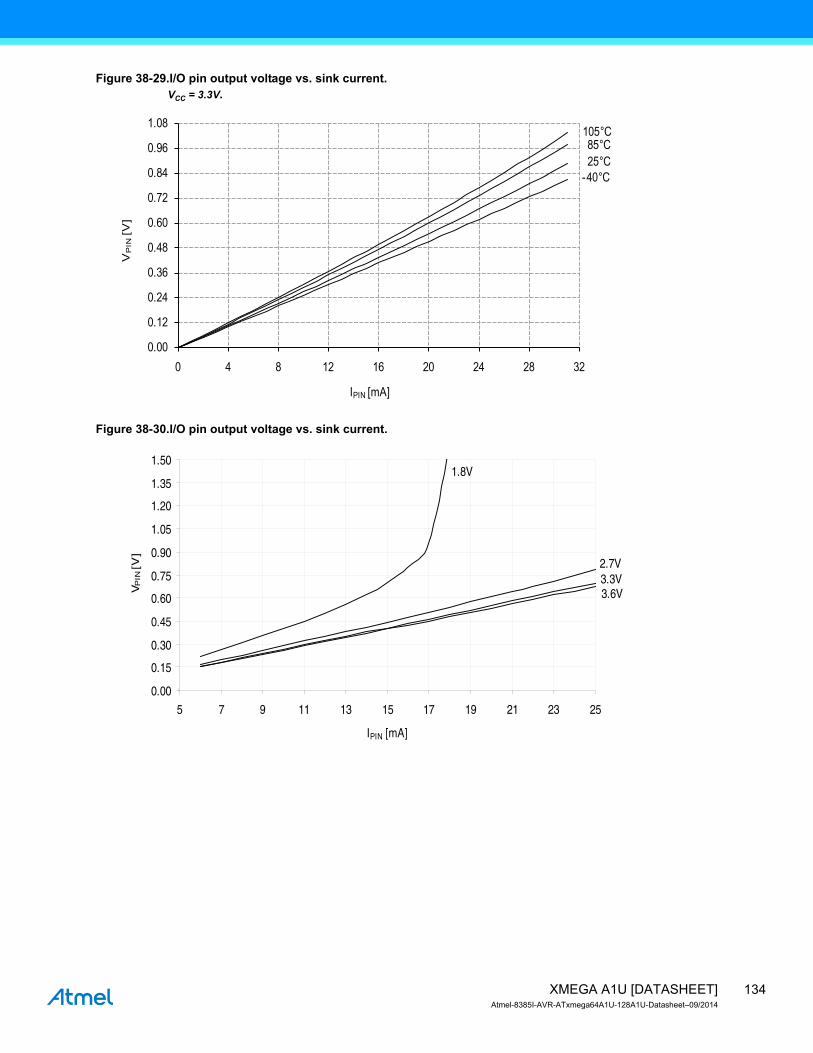
134XMEGA A1U [DATASHEET]Atmel-8385I-AVR-ATxmega64A1U-128A1U-Datasheet–09/2014
Figure 38-29.I/O pin output voltage vs. sink current.VCC = 3.3V.
Figure 38-30.I/O pin output voltage vs. sink current.
105 °C85 °C25 °C
-40 °C
0.00
0.12
0.24
0.36
0.48
0.60
0.72
0.84
0.96
1.08
0 4 8 12 16 20 24 28 32
VP
IN[V
]
IPIN [mA]
3.6V3.3V2.7V
0.00
0.15
0.30
0.45
0.60
0.75
0.90
1.05
1.20
1.35
1.50
5 7 9 11 13 15 17 19 21 23 25
IPIN [mA]
VP
IN [
V]
1.8V

135XMEGA A1U [DATASHEET]Atmel-8385I-AVR-ATxmega64A1U-128A1U-Datasheet–09/2014
38.1.2.3 Thresholds and Hysteresis
Figure 38-31.I/O pin input threshold voltage vs. VCC.T = 25°C.
Figure 38-32.I/O pin input threshold voltage vs. VCC.VIH I/O pin read as “1”.
VIL
VIH
0.50
0.65
0.80
0.95
1.10
1.25
1.40
1.55
1.70
1.85
1.6 1.8 2 2.2 2.4 2.6 2.8 3 3.2 3.4 3.6
VCC [V]
Vth
resh
old [
V]
85°C25°C-40°C
0.8
0.92
1.04
1.16
1.28
1.4
1.52
1.64
1.76
1.88
1.6 1.85 2.1 2.35 2.6 2.85 3.1 3.35 3.6
VCC [V]
Vth
resh
old [
V]
105°C
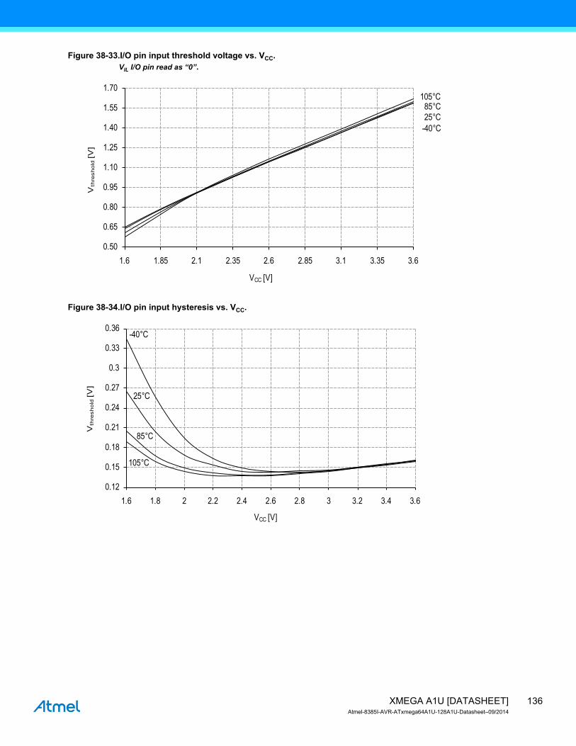
136XMEGA A1U [DATASHEET]Atmel-8385I-AVR-ATxmega64A1U-128A1U-Datasheet–09/2014
Figure 38-33.I/O pin input threshold voltage vs. VCC.VIL I/O pin read as “0”.
Figure 38-34.I/O pin input hysteresis vs. VCC.
105 °C85 °C25 °C
-40 °C
0.50
0.65
0.80
0.95
1.10
1.25
1.40
1.55
1.70
1.6 1.85 2.1 2.35 2.6 2.85 3.1 3.35 3.6
Vth
resh
old
[V]
VCC [V]
105 °C
85 °C
25 °C
-40 °C
0.12
0.15
0.18
0.21
0.24
0.27
0.3
0.33
0.36
1.6 1.8 2 2.2 2.4 2.6 2.8 3 3.2 3.4 3.6
Vth
resh
old
[V]
VCC [V]
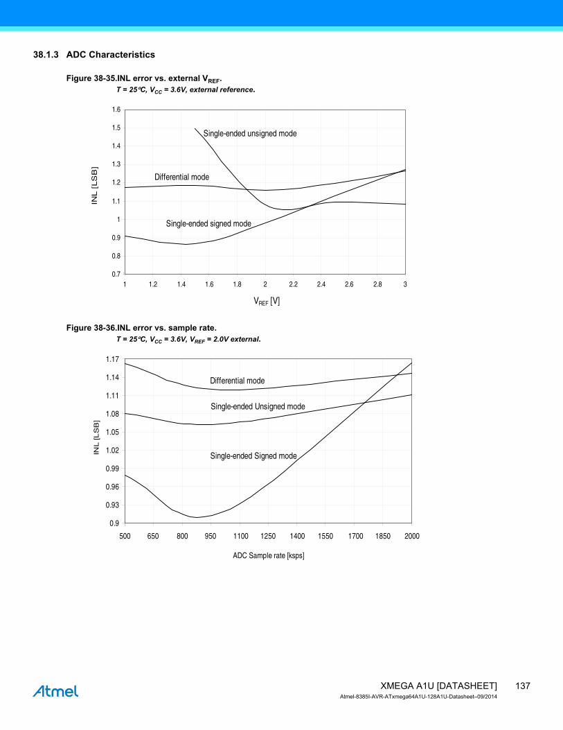
137XMEGA A1U [DATASHEET]Atmel-8385I-AVR-ATxmega64A1U-128A1U-Datasheet–09/2014
38.1.3 ADC Characteristics
Figure 38-35.INL error vs. external VREF.T = 25°C, VCC = 3.6V, external reference.
Figure 38-36.INL error vs. sample rate.T = 25°C, VCC = 3.6V, VREF = 2.0V external.
Single-ended unsigned mode
Single-ended signed mode
Differential mode
INL [
LS
B]
VREF [V]
0.7
0.8
0.9
1
1.1
1.2
1.3
1.4
1.5
1.6
1 1.2 1.4 1.6 1.8 2 2.2 2.4 2.6 2.8 3
Single-ended Unsigned mode
Single-ended Signed mode
Differential mode
0.9
0.93
0.96
0.99
1.02
1.05
1.08
1.11
1.14
1.17
500 650 800 950 1100 1250 1400 1550 1700 1850 2000
ADC Sample rate [ksps]
INL
[LS
B]
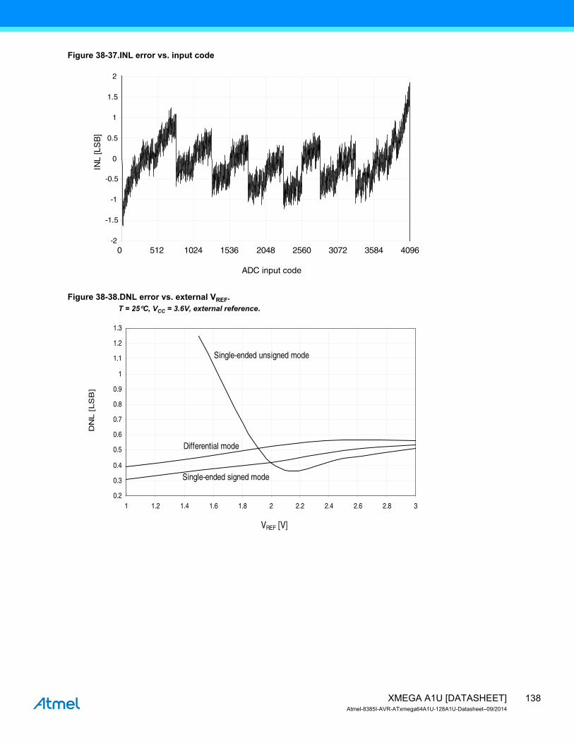
138XMEGA A1U [DATASHEET]Atmel-8385I-AVR-ATxmega64A1U-128A1U-Datasheet–09/2014
Figure 38-37.INL error vs. input code
Figure 38-38.DNL error vs. external VREF.T = 25°C, VCC = 3.6V, external reference.
-2
-1.5
-1
-0.5
0
0.5
1
1.5
2
0 512 1024 1536 2048 2560 3072 3584 4096
ADC input code
INL
[LS
B]
Single-ended unsigned mode
Single-ended signed mode
Differential mode
DN
L [
LS
B]
VREF [V]
0.2
0.3
0.4
0.5
0.6
0.7
0.8
0.9
1
1.1
1.2
1.3
1 1.2 1.4 1.6 1.8 2 2.2 2.4 2.6 2.8 3
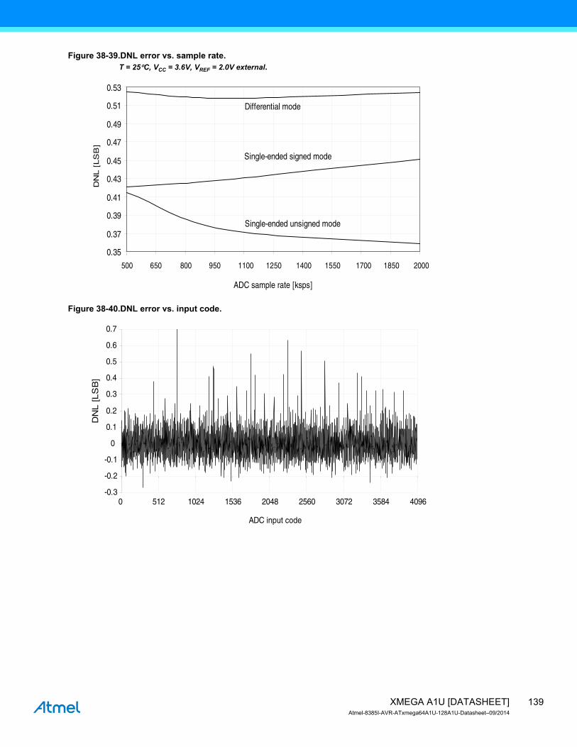
139XMEGA A1U [DATASHEET]Atmel-8385I-AVR-ATxmega64A1U-128A1U-Datasheet–09/2014
Figure 38-39.DNL error vs. sample rate.T = 25°C, VCC = 3.6V, VREF = 2.0V external.
Figure 38-40.DNL error vs. input code.
Single-ended unsigned mode
Single-ended signed mode
Differential mode
0.35
0.37
0.39
0.41
0.43
0.45
0.47
0.49
0.51
0.53
ADC sample rate [ksps]
DN
L [
LS
B]
500 650 800 950 1100 1250 1400 1550 1700 1850 2000
-0.3
-0.2
-0.1
0
0.1
0.2
0.3
0.4
0.5
0.6
0.7
0 512 1024 1536 2048 2560 3072 3584 4096
ADC input code
DN
L [
LS
B]
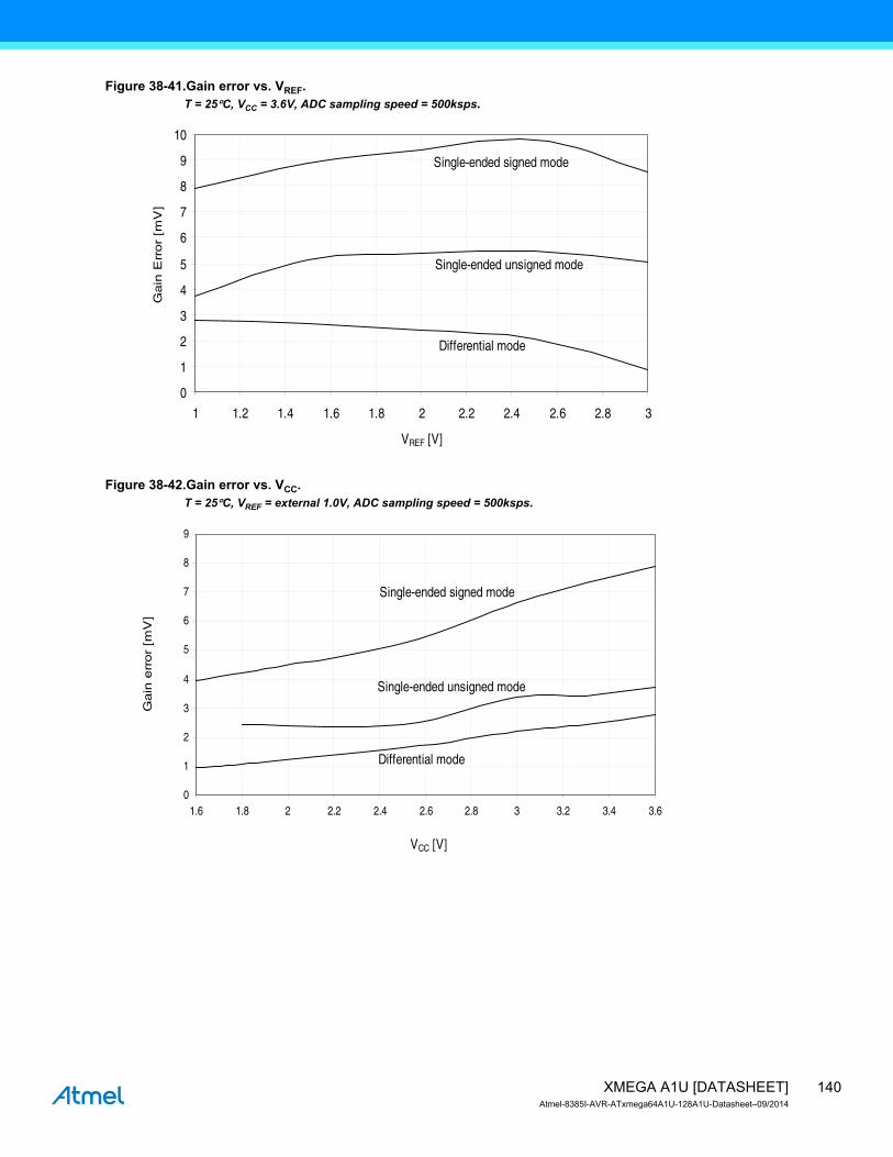
140XMEGA A1U [DATASHEET]Atmel-8385I-AVR-ATxmega64A1U-128A1U-Datasheet–09/2014
Figure 38-41.Gain error vs. VREF.T = 25°C, VCC = 3.6V, ADC sampling speed = 500ksps.
Figure 38-42.Gain error vs. VCC.T = 25°C, VREF = external 1.0V, ADC sampling speed = 500ksps.
Single-ended unsigned mode
Single-ended signed mode
Differential mode
0
1
2
3
4
5
6
7
8
9
10
1 1.2 1.4 1.6 1.8 2 2.2 2.4 2.6 2.8 3
VREF [V]
Gain
Err
or
[mV
]
0
1
2
3
4
5
6
7
8
9
1.6 1.8 2 2.2 2.4 2.6 2.8 3 3.2 3.4 3.6
Single-ended unsigned mode
Single-ended signed mode
Differential mode
VCC [V]
Gain
err
or
[mV
]
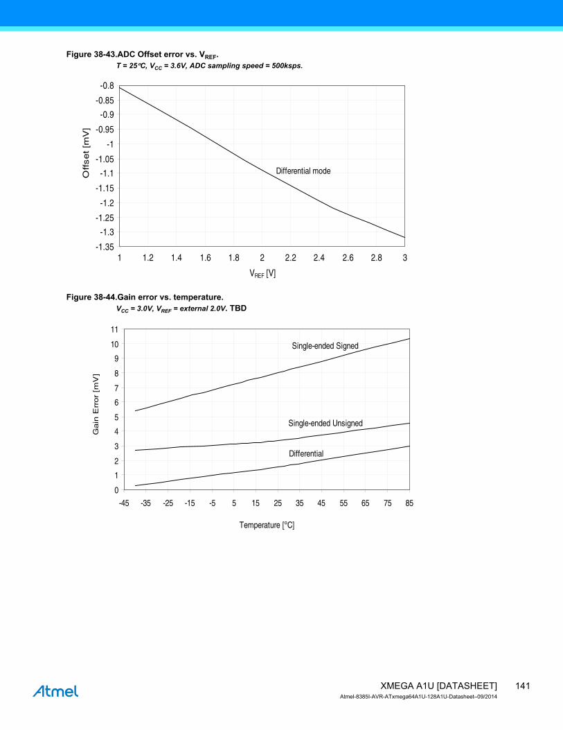
141XMEGA A1U [DATASHEET]Atmel-8385I-AVR-ATxmega64A1U-128A1U-Datasheet–09/2014
Figure 38-43.ADC Offset error vs. VREF.T = 25°C, VCC = 3.6V, ADC sampling speed = 500ksps.
Figure 38-44.Gain error vs. temperature.VCC = 3.0V, VREF = external 2.0V. TBD
Differential mode
-1.35
-1.3-1.25
-1.2
-1.15
-1.1-1.05
-1
-0.95
-0.9-0.85
-0.8
1 1.2 1.4 1.6 1.8 2 2.2 2.4 2.6 2.8 3
VREF [V]
Offset [m
V]
Single-ended Unsigned
Single-ended Signed
Differential
0
1
2
3
4
5
6
7
8
9
10
11
-45 -35 -25 -15 -5 5 15 25 35 45 55 65 75 85
Temperature [ºC]
Gain
Err
or
[mV
]

142XMEGA A1U [DATASHEET]Atmel-8385I-AVR-ATxmega64A1U-128A1U-Datasheet–09/2014
Figure 38-45.ADC Offset vs. VCC.T = 25°C, VREF = external 1.0V, ADC sampling speed = 500ksps.
Figure 38-46.Noise vs. VREF.T = 25°C, VCC = 3.6V, ADC sampling speed = 500ksps.
Differential mode
-0.7
-0.65
-0.6
-0.55
-0.5
-0.45
-0.4
-0.35
-0.3
-0.25
-0.2
1.6 1.8 2 2.2 2.4 2.6 2.8 3 3.2 3.4 3.6
VCC [V]
Offset [m
V]
Differential
0.37
0.38
0.39
0.4
0.41
0.42
0.43
0.44
0.45
0.46
0.47
1 1.2 1.4 1.6 1.8 2 2.2 2.4 2.6 2.8 3
VREF [V]
No
ise
[m
V R
MS
]

143XMEGA A1U [DATASHEET]Atmel-8385I-AVR-ATxmega64A1U-128A1U-Datasheet–09/2014
Figure 38-47.Noise vs. VCC.T = 25°C, VREF = external 1.0V, ADC sampling speed = 500ksps.
38.1.4 DAC Characteristics
Figure 38-48.DAC INL error vs. VREF.VCC = 3.6V, external reference, room temperature.
Differential
0.35
0.36
0.37
0.38
0.39
0.4
0.41
0.42
1.6 1.8 2 2.2 2.4 2.6 2.8 3 3.2 3.4 3.6
VCC [V]
No
ise
[m
V R
MS
]
1
1.1
1.2
1.3
1.4
1.5
1.6
1.7
1.8
1.9
1 1.2 1.4 1.6 1.8 2 2.2 2.4 2.6 2.8 3
VREF [V]
INL [LS
B]
25°C

144XMEGA A1U [DATASHEET]Atmel-8385I-AVR-ATxmega64A1U-128A1U-Datasheet–09/2014
Figure 38-49.DAC DNL error vs. VREF.VCC = 3.6V, external reference, room temperature.
Figure 38-50.DAC noise vs. temperature.VCC = 3.0V, VREF = 2.4V . TBD
0.55
0.65
0.75
0.85
0.95
1.05
1.15
1.25
1.35
1 1.2 1.4 1.6 1.8 2 2.2 2.4 2.6 2.8 3
VREF [V]
DN
L [
LS
B]
25°C
0.165
0.167
0.169
0.171
0.173
0.175
0.177
0.179
0.181
0.183
-45 -35 -25 -15 -5 5 15 25 35 45 55 65 75 85
Temperature [ºC]
Nois
e [m
V R
MS
]

145XMEGA A1U [DATASHEET]Atmel-8385I-AVR-ATxmega64A1U-128A1U-Datasheet–09/2014
38.1.5 Analog Comparator Characteristics
Figure 38-51.Analog comparator hysteresis vs. VCC.High-speed, small hysteresis.
Figure 38-52.Analog comparator hysteresis vs. VCC.Low power, small hysteresis.
105 C85 °C25 °C
-40 °C
35
37
39
41
43
45
47
49
51
53
1.6 1.8 2 2.2 2.4 2.6 2.8 3 3.2 3.4 3.6
VH
YS
T[m
V]
VCC [V]
°
105 °C85 °C
25 °C
-40 °C
25.0
26.5
28.0
29.5
31.0
32.5
34.0
35.5
37.0
1.6 1.8 2 2.2 2.4 2.6 2.8 3 3.2 3.4 3.6
VH
YS
T[m
V]
VCC [V]
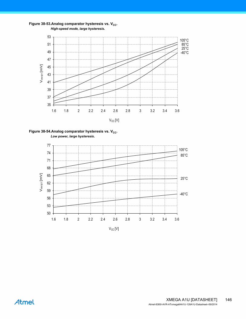
146XMEGA A1U [DATASHEET]Atmel-8385I-AVR-ATxmega64A1U-128A1U-Datasheet–09/2014
Figure 38-53.Analog comparator hysteresis vs. VCC.High-speed mode, large hysteresis.
Figure 38-54.Analog comparator hysteresis vs. VCC.Low power, large hysteresis.
105 C85 °C25 °C
-40 °C
35
37
39
41
43
45
47
49
51
53
1.6 1.8 2 2.2 2.4 2.6 2.8 3 3.2 3.4 3.6
VH
YS
T[m
V]
VCC [V]
°
105 °C85 °C
25 °C
-40 °C
50
53
56
59
62
65
68
71
74
77
1.6 1.8 2 2.2 2.4 2.6 2.8 3 3.2 3.4 3.6
VH
YS
T[m
V]
VCC [V]

147XMEGA A1U [DATASHEET]Atmel-8385I-AVR-ATxmega64A1U-128A1U-Datasheet–09/2014
Figure 38-55.Analog comparator current source vs. calibration value.Temperature = 25°C.
Figure 38-56.Analog comparator current source vs. calibration value.VCC = 3.0V.
3.3V3.0V2.7V
2.2V1.8V
2
3
4
5
6
7
8
0 1 2 3 4 5 6 7 8 9 10 11 12 13 14 15
CALIB[3..0]
I [µ
A]
105 °C85 °C25 °C
-40°C
3.0
3.3
3.6
3.9
4.2
4.5
4.8
5.1
5.4
5.7
6.0
0 2 4 6 8 10 12 14 16
I CU
RR
EN
TSO
UR
CE
[µA
]
CALIB[3..0]

148XMEGA A1U [DATASHEET]Atmel-8385I-AVR-ATxmega64A1U-128A1U-Datasheet–09/2014
Figure 38-57.Voltage scaler INL vs. SCALEFAC.T = 25°C, VCC = 3.0V.
38.1.6 Internal 1.0V reference Characteristics
Figure 38-58. ADC/DAC Internal 1.0V reference vs. temperature.
-0.10
-0.05
0.00
0.05
0.10
0.15
0.20
0.25
0.30
0 7 14 21 28 35 42 49 56 63
SCALEFAC
INL [
LS
B]
25°C
3.6 V3.3 V3.0 V2.7 V1.8 V1.6 V
0.9750.9780.9810.9840.9870.9900.9930.9960.9991.0021.005
-40 -25 -10 5 20 35 50 65 80 95 110
Ban
dgap
Vol
tage
[V
]
Temperature [°C]
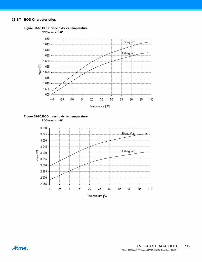
149XMEGA A1U [DATASHEET]Atmel-8385I-AVR-ATxmega64A1U-128A1U-Datasheet–09/2014
38.1.7 BOD Characteristics
Figure 38-59.BOD thresholds vs. temperature.BOD level = 1.6V.
Figure 38-60.BOD thresholds vs. temperature.BOD level = 3.0V.
Rising Vcc
Falling Vcc
1.600
1.605
1.610
1.615
1.620
1.625
1.630
1.635
1.640
1.645
1.650
-40 -25 -10 5 20 35 50 65 80 95 110
VB
OT
[V]
Temperature [°C]
Rising Vcc
Falling Vcc
2.955
2.970
2.985
3.000
3.015
3.030
3.045
3.060
3.075
3.090
-40 -25 -10 5 20 35 50 65 80 95 110
VB
OT
[V]
Temperature [°C]
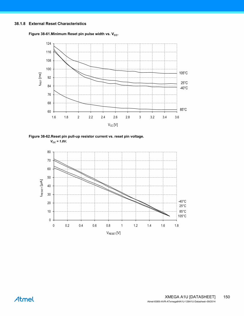
150XMEGA A1U [DATASHEET]Atmel-8385I-AVR-ATxmega64A1U-128A1U-Datasheet–09/2014
38.1.8 External Reset Characteristics
Figure 38-61.Minimum Reset pin pulse width vs. VCC.
Figure 38-62.Reset pin pull-up resistor current vs. reset pin voltage.VCC = 1.8V.
105°C
85°C
25°C-40°C
60
68
76
84
92
100
108
116
124
1.6 1.8 2 2.2 2.4 2.6 2.8 3 3.2 3.4 3.6
t RS
T[n
s]
VCC [V]
105°C85°C25°C
-40°C
0
10
20
30
40
50
60
70
80
0 0.2 0.4 0.6 0.8 1 1.2 1.4 1.6 1.8
I RE
SE
T[µ
A]
VRESET [V]
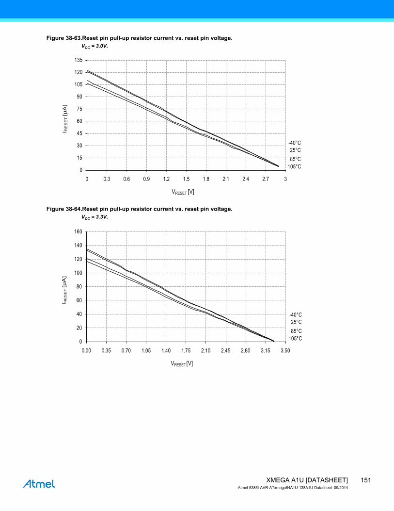
151XMEGA A1U [DATASHEET]Atmel-8385I-AVR-ATxmega64A1U-128A1U-Datasheet–09/2014
Figure 38-63.Reset pin pull-up resistor current vs. reset pin voltage.VCC = 3.0V.
Figure 38-64.Reset pin pull-up resistor current vs. reset pin voltage.VCC = 3.3V.
0
15
30
45
60
75
90
105
120
135
0 0.3 0.6 0.9 1.2 1.5 1.8 2.1 2.4 2.7 3
I RE
SE
T[µ
A]
VRESET [V]
105°C85°C25°C
-40°C
0
20
40
60
80
100
120
140
160
0.00 0.35 0.70 1.05 1.40 1.75 2.10 2.45 2.80 3.15 3.50
I RE
SE
T[µ
A]
VRESET [V]
105°C85°C25°C
-40°C
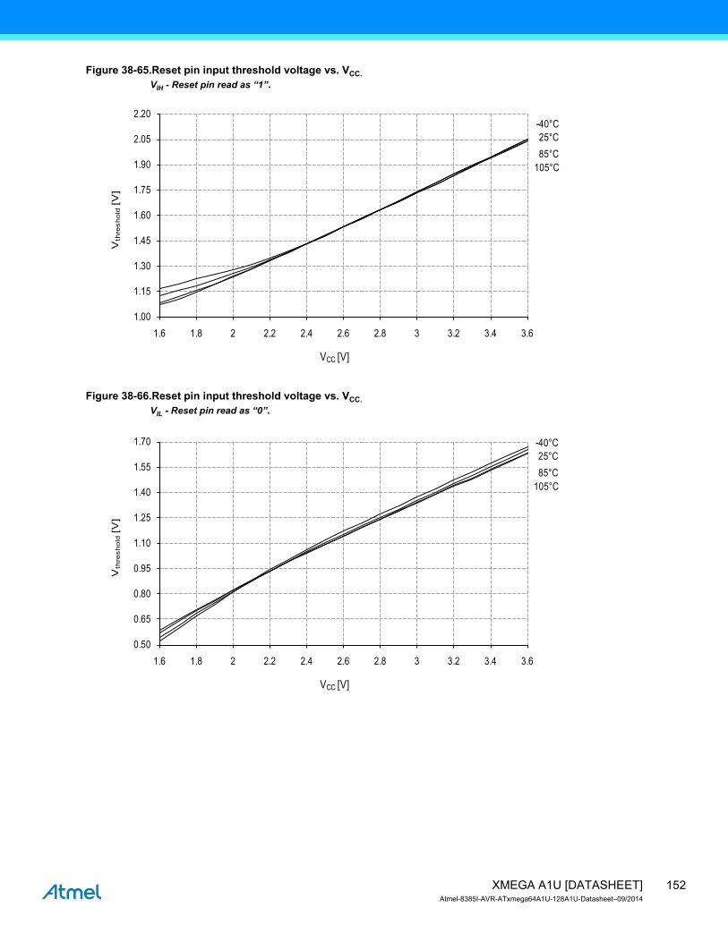
152XMEGA A1U [DATASHEET]Atmel-8385I-AVR-ATxmega64A1U-128A1U-Datasheet–09/2014
Figure 38-65.Reset pin input threshold voltage vs. VCC.VIH - Reset pin read as “1”.
Figure 38-66.Reset pin input threshold voltage vs. VCC.VIL - Reset pin read as “0”.
1.00
1.15
1.30
1.45
1.60
1.75
1.90
2.05
2.20
1.6 1.8 2 2.2 2.4 2.6 2.8 3 3.2 3.4 3.6
Vth
resh
old
[V]
VCC [V]
105°C85°C25°C
-40°C
0.50
0.65
0.80
0.95
1.10
1.25
1.40
1.55
1.70
1.6 1.8 2 2.2 2.4 2.6 2.8 3 3.2 3.4 3.6
Vth
resh
old
[V]
VCC [V]
105°C85°C25°C
-40°C

153XMEGA A1U [DATASHEET]Atmel-8385I-AVR-ATxmega64A1U-128A1U-Datasheet–09/2014
38.1.9 Power-on Reset Characteristics
Figure 38-67.Power-on reset current consumption vs. VCC.BOD level = 3.0V, enabled in continuous mode.
Figure 38-68.Power-on reset current consumption vs. VCC.BOD level = 3.0V, enabled in sampled mode.
105°C85°C25°C
-40°C
0
150
300
450
600
750
900
1050
1200
1350
1500
0 0.3 0.6 0.9 1.2 1.5 1.8 2.1 2.4 2.7 3
I CC
[µA
]
VCC [V]
0
150
300
450
600
750
900
1050
1200
1350
0 0.3 0.6 0.9 1.2 1.5 1.8 2.1 2.4 2.7 3
I CC
[µA
]
VCC [V]
105°C85°C25°C
-40°C
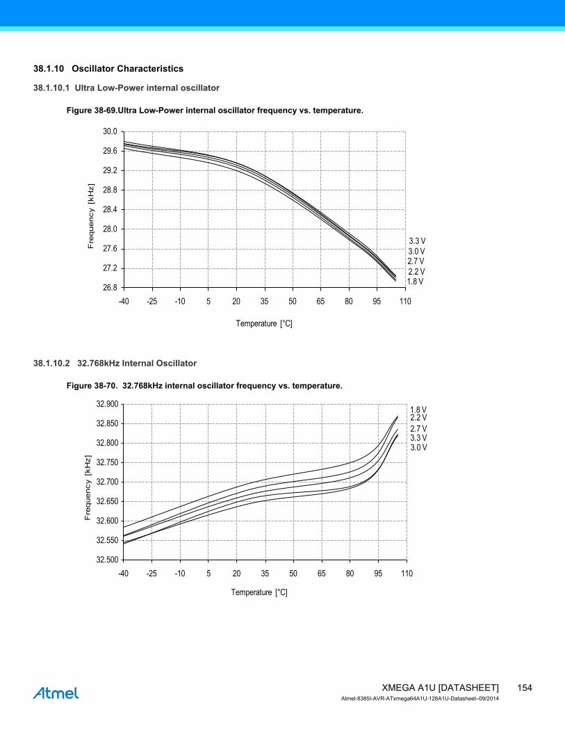
154XMEGA A1U [DATASHEET]Atmel-8385I-AVR-ATxmega64A1U-128A1U-Datasheet–09/2014
38.1.10 Oscillator Characteristics
38.1.10.1 Ultra Low-Power internal oscillator
Figure 38-69.Ultra Low-Power internal oscillator frequency vs. temperature.
38.1.10.2 32.768kHz Internal Oscillator
Figure 38-70. 32.768kHz internal oscillator frequency vs. temperature.
3.3 V3.0 V2.7 V2.2 V1.8 V26.8
27.2
27.6
28.0
28.4
28.8
29.2
29.6
30.0
-40 -25 -10 5 20 35 50 65 80 95 110
Fre
quen
cy [
kHz]
Temperature [°C]
3.3 V3.0 V
2.7 V2.2 V1.8 V
32.500
32.550
32.600
32.650
32.700
32.750
32.800
32.850
32.900
-40 -25 -10 5 20 35 50 65 80 95 110
Fre
quen
cy [
kHz]
Temperature [°C]

155XMEGA A1U [DATASHEET]Atmel-8385I-AVR-ATxmega64A1U-128A1U-Datasheet–09/2014
Figure 38-71. 32.768kHz internal oscillator frequency vs. calibration value.VCC = 3.0V, T = 25°C.
38.1.10.3 2MHz Internal Oscillator
Figure 38-72. 2MHz internal oscillator frequency vs. temperature.DFLL disabled.
20
23
26
29
32
35
38
41
44
47
50
0 30 60 90 120 150 180 210 240 270
RC32KCAL[7..0]
Fre
quency [
kH
z]
3.3 V3.0 V2.7 V2.2 V1.8 V
1.98
1.99
2.00
2.01
2.02
2.03
2.04
2.05
2.06
2.07
-40 -25 -10 5 20 35 50 65 80 95 110
Fre
quen
cy [
MH
z]
Temperature [°C]
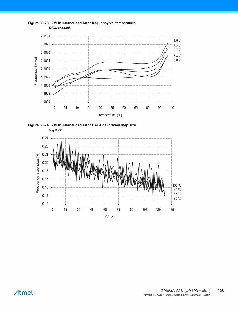
156XMEGA A1U [DATASHEET]Atmel-8385I-AVR-ATxmega64A1U-128A1U-Datasheet–09/2014
Figure 38-73. 2MHz internal oscillator frequency vs. temperature.DFLL enabled.
Figure 38-74. 2MHz internal oscillator CALA calibration step size.VCC = 3V.
3.3 V3.0 V
2.7 V2.2 V1.8 V
1.9900
1.9925
1.9950
1.9975
2.0000
2.0025
2.0050
2.0075
2.0100
-40 -25 -10 5 20 35 50 65 80 95 110
Fre
quen
cy [
MH
z]
Temperature [°C]
105 °C
85 °C25 °C
-40 °C
0.12
0.14
0.15
0.17
0.18
0.20
0.21
0.23
0.24
0 15 30 45 60 75 90 105 120 135
Fre
quen
cy s
tep
size
[%]
CALA
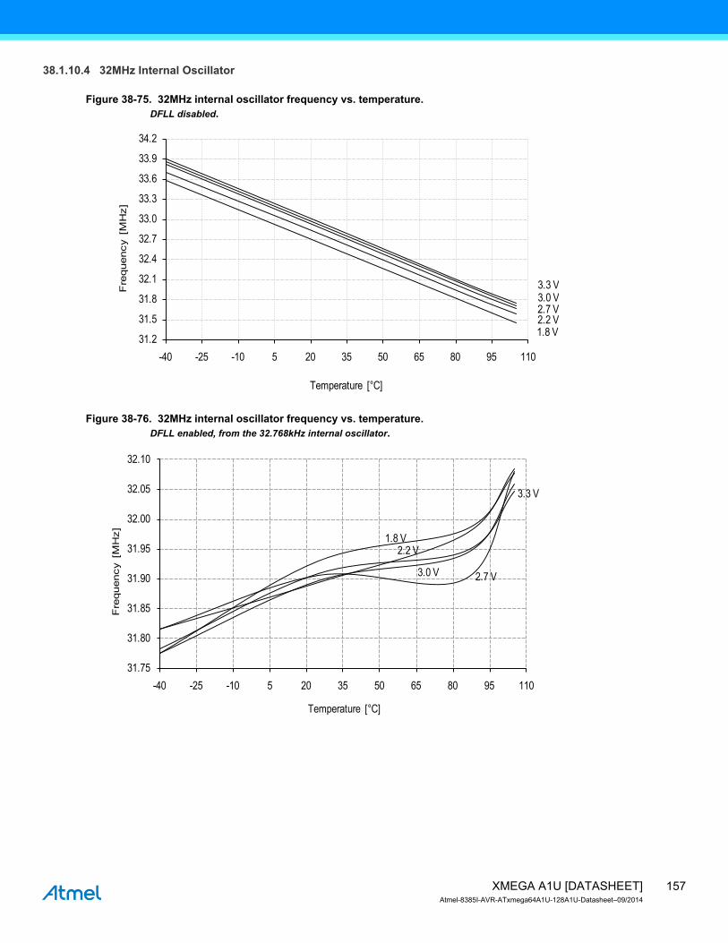
157XMEGA A1U [DATASHEET]Atmel-8385I-AVR-ATxmega64A1U-128A1U-Datasheet–09/2014
38.1.10.4 32MHz Internal Oscillator
Figure 38-75. 32MHz internal oscillator frequency vs. temperature.DFLL disabled.
Figure 38-76. 32MHz internal oscillator frequency vs. temperature.DFLL enabled, from the 32.768kHz internal oscillator.
3.3 V3.0 V2.7 V2.2 V1.8 V31.2
31.5
31.8
32.1
32.4
32.7
33.0
33.3
33.6
33.9
34.2
-40 -25 -10 5 20 35 50 65 80 95 110
Fre
quen
cy [
MH
z]
Temperature [°C]
3.3 V
3.0 V 2.7 V
2.2 V1.8 V
31.75
31.80
31.85
31.90
31.95
32.00
32.05
32.10
-40 -25 -10 5 20 35 50 65 80 95 110
Fre
quen
cy [
MH
z]
Temperature [°C]
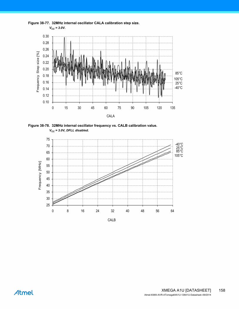
158XMEGA A1U [DATASHEET]Atmel-8385I-AVR-ATxmega64A1U-128A1U-Datasheet–09/2014
Figure 38-77. 32MHz internal oscillator CALA calibration step size.VCC = 3.0V.
Figure 38-78. 32MHz internal oscillator frequency vs. CALB calibration value.VCC = 3.0V, DFLL disabled.
105 °C85°C
25 °C-40 °C
0.10
0.12
0.14
0.16
0.18
0.20
0.22
0.24
0.26
0.28
0.30
0 15 30 45 60 75 90 105 120 135
Fre
quen
cy S
tep
size
[%]
CALA
105 °C85 °C25 °C
-40 °C
25
30
35
40
45
50
55
60
65
70
75
0 8 16 24 32 40 48 56 64
Fre
quen
cy [
MH
z]
CALB
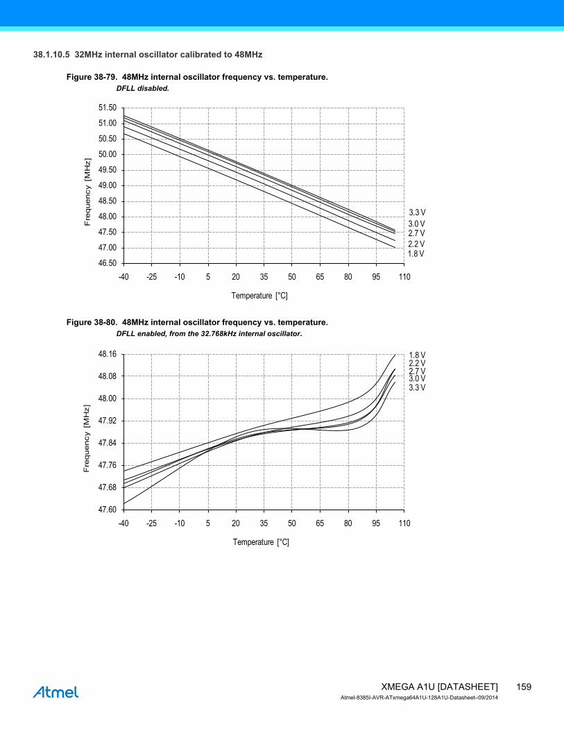
159XMEGA A1U [DATASHEET]Atmel-8385I-AVR-ATxmega64A1U-128A1U-Datasheet–09/2014
38.1.10.5 32MHz internal oscillator calibrated to 48MHz
Figure 38-79. 48MHz internal oscillator frequency vs. temperature.DFLL disabled.
Figure 38-80. 48MHz internal oscillator frequency vs. temperature.DFLL enabled, from the 32.768kHz internal oscillator.
3.3 V3.0 V2.7 V2.2 V1.8 V
46.50
47.00
47.50
48.00
48.50
49.00
49.50
50.00
50.50
51.00
51.50
-40 -25 -10 5 20 35 50 65 80 95 110
Fre
quen
cy [
MH
z]
Temperature [°C]
3.3 V3.0 V2.7 V2.2 V1.8 V
47.60
47.68
47.76
47.84
47.92
48.00
48.08
48.16
-40 -25 -10 5 20 35 50 65 80 95 110
Fre
quen
cy [
MH
z]
Temperature [°C]

160XMEGA A1U [DATASHEET]Atmel-8385I-AVR-ATxmega64A1U-128A1U-Datasheet–09/2014
Figure 38-81. 32MHz internal oscillator CALA calibration step size.Using 48MHz calibration value from signature row, VCC = 3.0V.
38.1.11 PDI characteristics
Figure 38-82. Maximum PDI frequency vs. VCC.
105 °C85 °C25 °C
-40 °C
0.10
0.12
0.14
0.16
0.18
0.20
0.22
0.24
0.26
0.28
0.30
0 15 30 45 60 75 90 105 120 135
Fre
quen
cy S
tep
size
[%]
CALA
105 °C85 °C25 °C
-40 °C
10
13
16
19
22
25
28
31
34
1.6 1.8 2 2.2 2.4 2.6 2.8 3 3.2 3.4 3.6
f MA
X[M
Hz]
VCC [V]
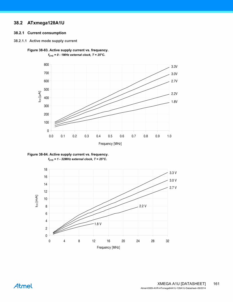
161XMEGA A1U [DATASHEET]Atmel-8385I-AVR-ATxmega64A1U-128A1U-Datasheet–09/2014
38.2 ATxmega128A1U
38.2.1 Current consumption
38.2.1.1 Active mode supply current
Figure 38-83. Active supply current vs. frequency.fSYS = 0 - 1MHz external clock, T = 25°C.
Figure 38-84. Active supply current vs. frequency.fSYS = 1 - 32MHz external clock, T = 25°C.
3.3V
3.0V
2.7V
2.2V
1.8V
0
100
200
300
400
500
600
700
800
0.0 0.1 0.2 0.3 0.4 0.5 0.6 0.7 0.8 0.9 1.0
Frequency [MHz]
I CC
[µA
]
3.3 V
3.0 V
2.7 V
1.8 V
0
2
4
6
8
10
12
14
16
18
0 4 8 12 16 20 24 28 32
Frequency [MHz]
I CC
[mA
]
2.2 V
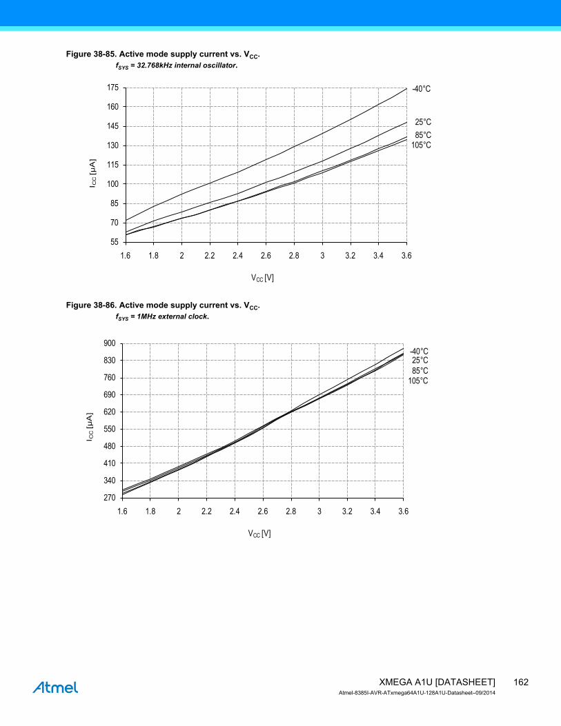
162XMEGA A1U [DATASHEET]Atmel-8385I-AVR-ATxmega64A1U-128A1U-Datasheet–09/2014
Figure 38-85. Active mode supply current vs. VCC.fSYS = 32.768kHz internal oscillator.
Figure 38-86. Active mode supply current vs. VCC.fSYS = 1MHz external clock.
105 °C85 °C25 °C
-40 °C
55
70
85
100
115
130
145
160
175
1.6 1.8 2 2.2 2.4 2.6 2.8 3 3.2 3.4 3.6
I CC
[µA
]
VCC [V]
105 °C85 °C25 °C
-40 °C
270
340
410
480
550
620
690
760
830
900
1.6 1.8 2 2.2 2.4 2.6 2.8 3 3.2 3.4 3.6
I CC
[µA
]
VCC [V]

163XMEGA A1U [DATASHEET]Atmel-8385I-AVR-ATxmega64A1U-128A1U-Datasheet–09/2014
Figure 38-87. Active mode supply current vs. VCC.fSYS = 2MHz internal oscillator.
Figure 38-88. Active mode supply current vs. VCC.fSYS = 32MHz internal oscillator prescaled to 8MHz.
105 °C85 °C25 °C
-40 °C
600
750
900
1050
1200
1350
1500
1650
1800
1.6 1.8 2 2.2 2.4 2.6 2.8 3 3.2 3.4 3.6
I CC
[µA
]
VCC [V]
105 °C85 °C25 °C
-40 °C
2.1
2.7
3.3
3.9
4.5
5.1
5.7
6.3
6.9
7.5
1.6 1.8 2 2.2 2.4 2.6 2.8 3 3.2 3.4 3.6
I CC
[mA
]
VCC [V]

164XMEGA A1U [DATASHEET]Atmel-8385I-AVR-ATxmega64A1U-128A1U-Datasheet–09/2014
Figure 38-89. Active mode supply current vs. VCC.fSYS = 32MHz internal oscillator.
38.2.1.2 Idle mode supply current
Figure 38-90.Idle mode supply current vs. frequency.fSYS = 0 - 1MHz external clock, T = 25°C.
105 °C85 °C25 °C
-40 °C
13
14
15
16
17
18
19
20
21
2.7 2.8 2.9 3 3.1 3.2 3.3 3.4 3.5 3.6
I CC
[mA
]
VCC [V]
3.3 V
3.0 V
2.7 V
2.2 V
1.8 V
0
25
50
75
100
125
150
175
200
225
250
0 0.1 0.2 0.3 0.4 0.5 0.6 0.7 0.8 0.9 1
Frequency [MHz]
I CC
[µA
]
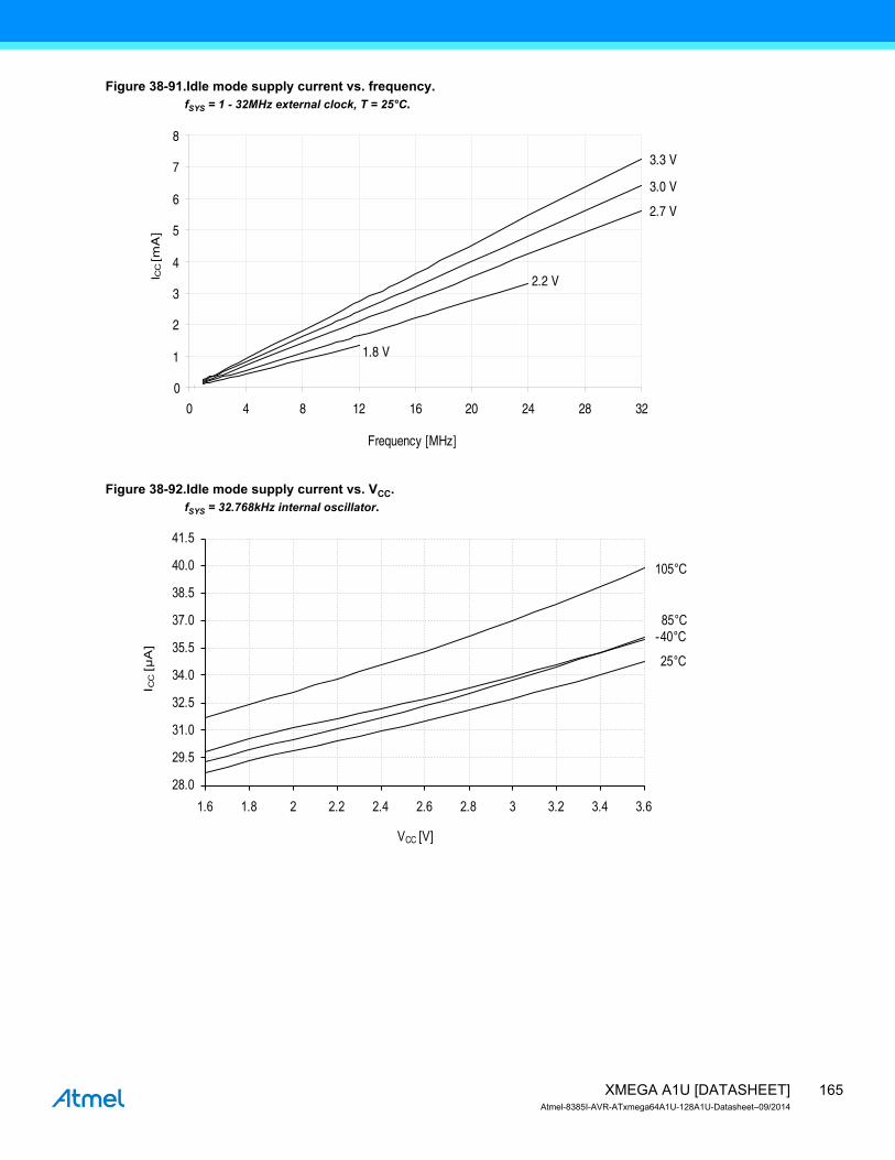
165XMEGA A1U [DATASHEET]Atmel-8385I-AVR-ATxmega64A1U-128A1U-Datasheet–09/2014
Figure 38-91.Idle mode supply current vs. frequency.fSYS = 1 - 32MHz external clock, T = 25°C.
Figure 38-92.Idle mode supply current vs. VCC.fSYS = 32.768kHz internal oscillator.
3.3 V
3.0 V
2.7 V
1.8 V
0
1
2
3
4
5
6
7
8
0 4 8 12 16 20 24 28 32
Frequency [MHz]
I CC
[mA
]
2.2 V
105 °C
85 °C
25 °C
-40 °C
28.0
29.5
31.0
32.5
34.0
35.5
37.0
38.5
40.0
41.5
1.6 1.8 2 2.2 2.4 2.6 2.8 3 3.2 3.4 3.6
I CC
[µA
]
VCC [V]

166XMEGA A1U [DATASHEET]Atmel-8385I-AVR-ATxmega64A1U-128A1U-Datasheet–09/2014
Figure 38-93.Idle mode supply current vs. VCC.fSYS = 1MHz external clock.
Figure 38-94.Idle mode supply current vs. VCC.fSYS = 2MHz internal oscillator.
105 °C85 °C25 °C
-40 °C
90
110
130
150
170
190
210
230
250
270
1.6 1.8 2 2.2 2.4 2.6 2.8 3 3.2 3.4 3.6
I CC
[µA
]
VCC [V]
105 °C85 °C25 °C
-40 °C
250
300
350
400
450
500
550
600
1.6 1.8 2 2.2 2.4 2.6 2.8 3 3.2 3.4 3.6
I CC
[µA
]
VCC [V]
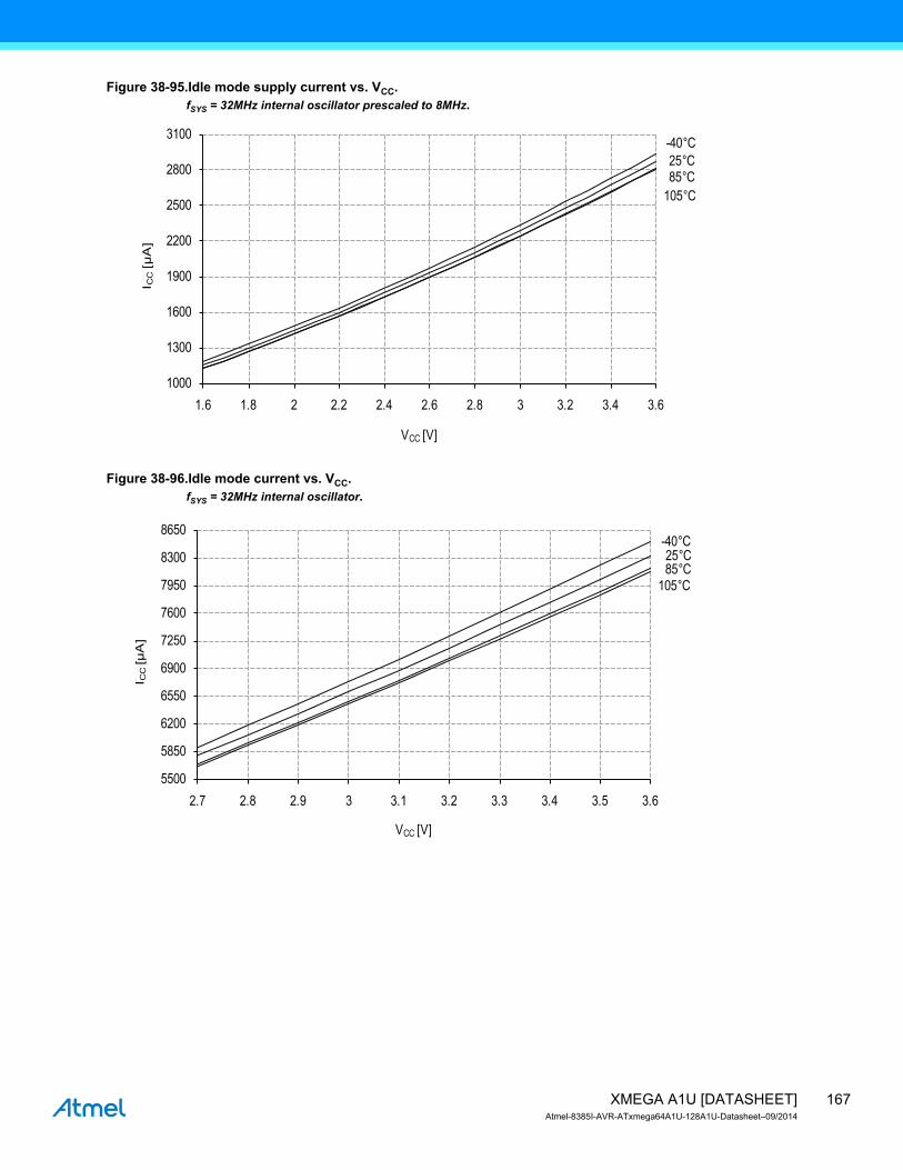
167XMEGA A1U [DATASHEET]Atmel-8385I-AVR-ATxmega64A1U-128A1U-Datasheet–09/2014
Figure 38-95.Idle mode supply current vs. VCC.fSYS = 32MHz internal oscillator prescaled to 8MHz.
Figure 38-96.Idle mode current vs. VCC.fSYS = 32MHz internal oscillator.
105 °C85 °C25 °C-40 °C
1000
1300
1600
1900
2200
2500
2800
3100
1.6 1.8 2 2.2 2.4 2.6 2.8 3 3.2 3.4 3.6
I CC
[µA
]
VCC [V]
105 °C85 °C25 °C
-40 °C
5500
5850
6200
6550
6900
7250
7600
7950
8300
8650
2.7 2.8 2.9 3 3.1 3.2 3.3 3.4 3.5 3.6
I CC
[µA
]
VCC [V]
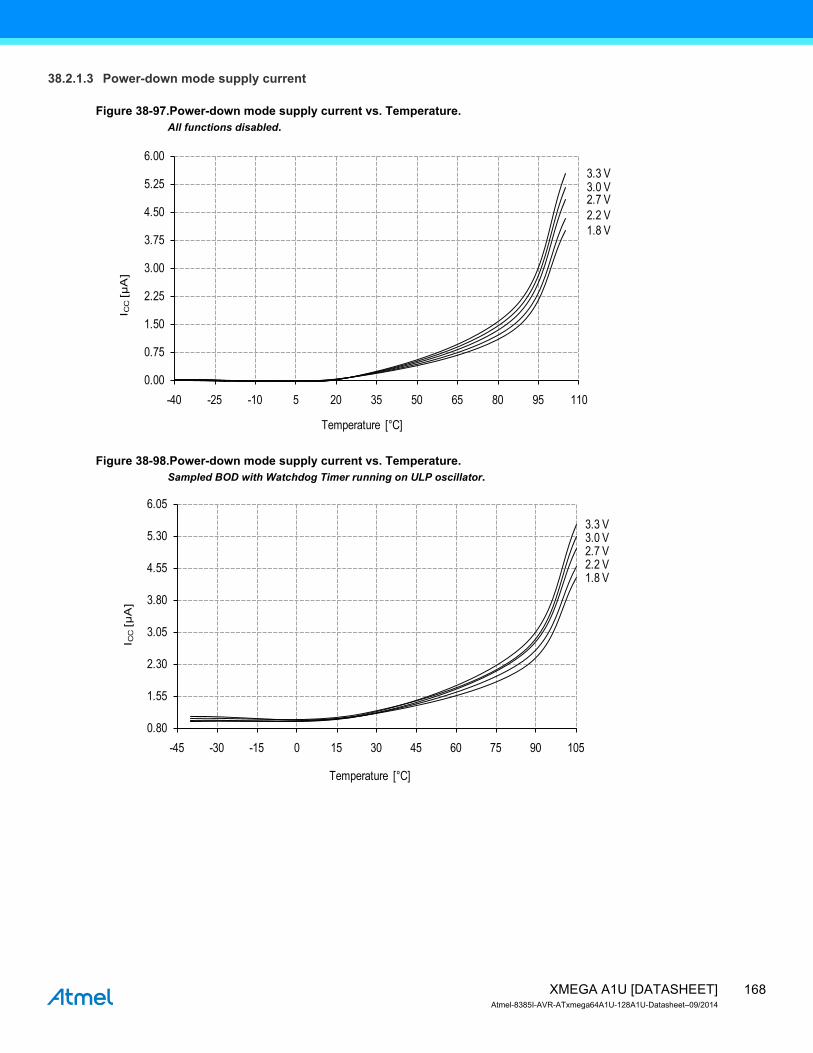
168XMEGA A1U [DATASHEET]Atmel-8385I-AVR-ATxmega64A1U-128A1U-Datasheet–09/2014
38.2.1.3 Power-down mode supply current
Figure 38-97.Power-down mode supply current vs. Temperature.All functions disabled.
Figure 38-98.Power-down mode supply current vs. Temperature.Sampled BOD with Watchdog Timer running on ULP oscillator.
3.3 V3.0 V2.7 V2.2 V1.8 V
0.00
0.75
1.50
2.25
3.00
3.75
4.50
5.25
6.00
-40 -25 -10 5 20 35 50 65 80 95 110
I CC
[µA
]
Temperature [°C]
3.3 V3.0 V2.7 V2.2 V1.8 V
0.80
1.55
2.30
3.05
3.80
4.55
5.30
6.05
-45 -30 -15 0 15 30 45 60 75 90 105
I CC
[µA
]
Temperature [°C]
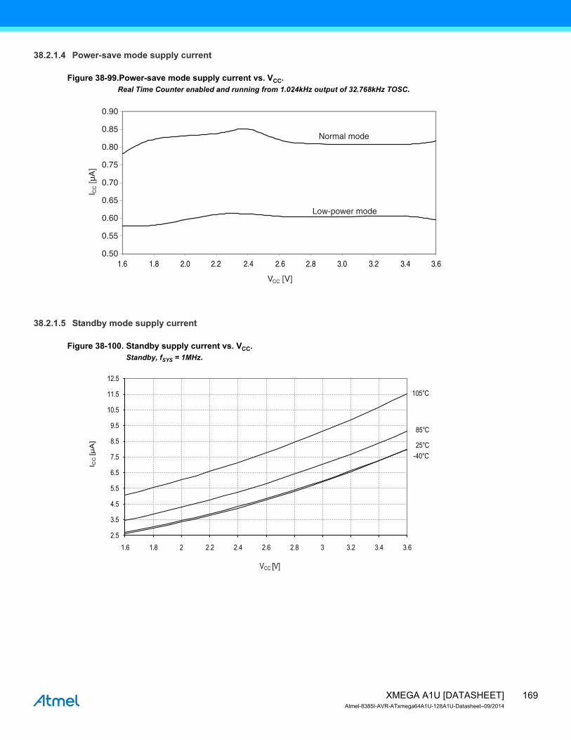
169XMEGA A1U [DATASHEET]Atmel-8385I-AVR-ATxmega64A1U-128A1U-Datasheet–09/2014
38.2.1.4 Power-save mode supply current
Figure 38-99.Power-save mode supply current vs. VCC.Real Time Counter enabled and running from 1.024kHz output of 32.768kHz TOSC.
38.2.1.5 Standby mode supply current
Figure 38-100. Standby supply current vs. VCC.Standby, fSYS = 1MHz.
Normal mode
Low-power mode
0.50
0.55
0.60
0.65
0.70
0.75
0.80
0.85
0.90
VCC [V]
I CC [µ
A]
1.6 1.8 2.0 2.2 2.4 2.6 2.8 3.0 3.2 3.4 3.6
105°C
85°C
25°C-40°C
2.5
3.5
4.5
5.5
6.5
7.5
8.5
9.5
10.5
11.5
12.5
1.6 1.8 2 2.2 2.4 2.6 2.8 3 3.2 3.4 3.6
I CC
[µA
]
VCC [V]
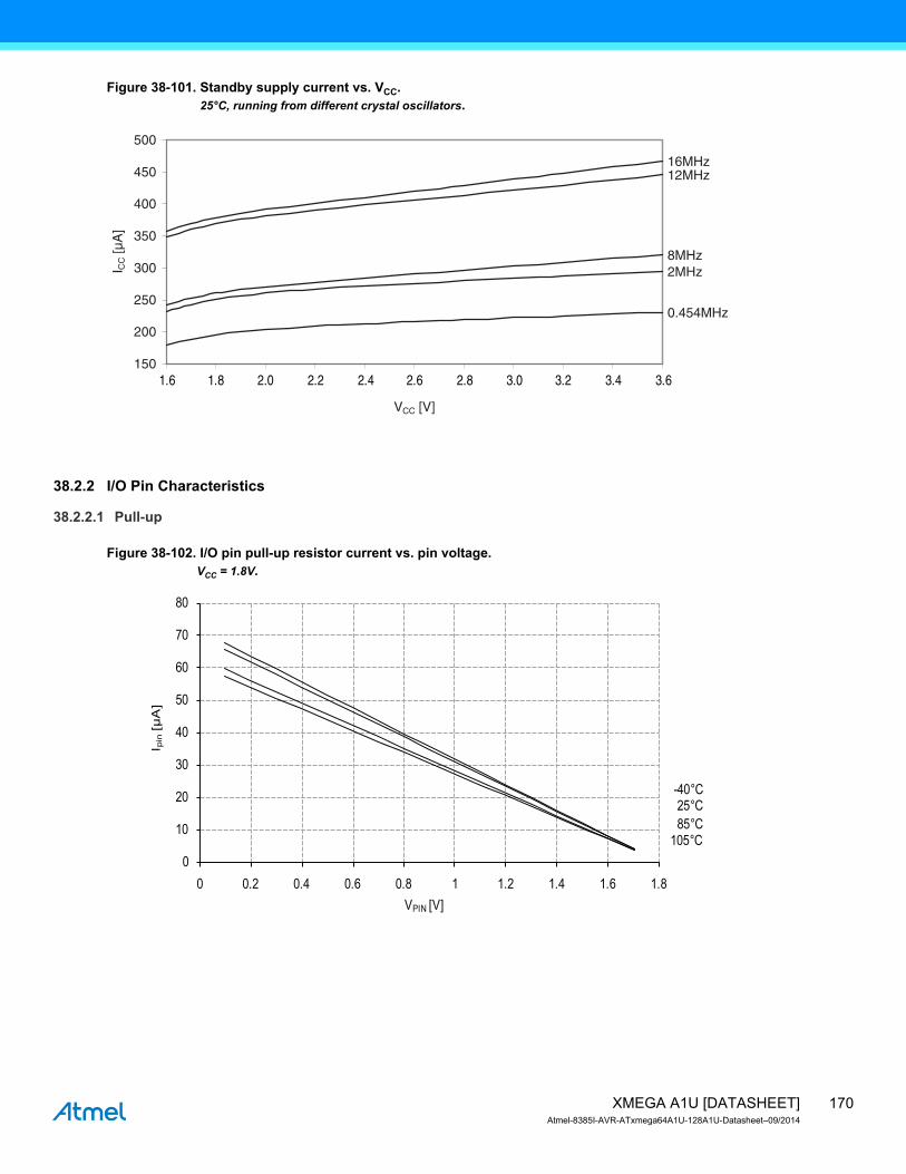
170XMEGA A1U [DATASHEET]Atmel-8385I-AVR-ATxmega64A1U-128A1U-Datasheet–09/2014
Figure 38-101. Standby supply current vs. VCC.25°C, running from different crystal oscillators.
38.2.2 I/O Pin Characteristics
38.2.2.1 Pull-up
Figure 38-102. I/O pin pull-up resistor current vs. pin voltage. VCC = 1.8V.
16MHz12MHz
8MHz2MHz
0.454MHz
150
200
250
300
350
400
450
500
VCC [V]
I CC [µ
A]
1.6 1.8 2.0 2.2 2.4 2.6 2.8 3.0 3.2 3.4 3.6
105 °C85 °C25 °C
-40 °C
0
10
20
30
40
50
60
70
80
0 0.2 0.4 0.6 0.8 1 1.2 1.4 1.6 1.8
I pin
[µA
]
VPIN [V]

171XMEGA A1U [DATASHEET]Atmel-8385I-AVR-ATxmega64A1U-128A1U-Datasheet–09/2014
Figure 38-103. I/O pin pull-up resistor current vs. pin voltage.VCC = 3.0V.
Figure 38-104. I/O pin pull-up resistor current vs. pin voltage.VCC = 3.3V.
0
15
30
45
60
75
90
105
120
0 0.3 0.6 0.9 1.2 1.5 1.8 2.1 2.4 2.7 3
I pin
[µA
]
VPIN [V]
105 °C85 °C25 °C
-40 °C
0
20
40
60
80
100
120
140
0 0.3 0.6 0.9 1.2 1.5 1.8 2.1 2.4 2.7 3 3.3
I pin
[µA
]
VPIN [V]
105 °C85 °C25 °C
-40 °C

172XMEGA A1U [DATASHEET]Atmel-8385I-AVR-ATxmega64A1U-128A1U-Datasheet–09/2014
38.2.2.2 Output Voltage vs. Sink/Source Current
Figure 38-105.I/O pin output voltage vs. source current.VCC = 1.8V.
Figure 38-106.I/O pin output voltage vs. source current.VCC = 3.0V.
105 °C85 °C25 °C-40°C
0.50
0.65
0.80
0.95
1.10
1.25
1.40
1.55
1.70
1.85
-10 -9 -8 -7 -6 -5 -4 -3 -2 -1 0
VP
IN[V
]
IPIN [mA]
105 °C85 °C
25 °C
-40 °C
0.5
0.8
1.1
1.4
1.7
2.0
2.3
2.6
2.9
3.2
-30 -27 -24 -21 -18 -15 -12 -9 -6 -3 0
VP
IN[V
]
IPIN [mA]

173XMEGA A1U [DATASHEET]Atmel-8385I-AVR-ATxmega64A1U-128A1U-Datasheet–09/2014
Figure 38-107.I/O pin output voltage vs. source current.VCC = 3.3V.
Figure 38-108.I/O pin output voltage vs. source current.
105 °C
85 °C
25 °C
-40 °C
0.5
0.8
1.1
1.4
1.7
2.0
2.3
2.6
2.9
3.2
3.5
-30 -27 -24 -21 -18 -15 -12 -9 -6 -3 0
VP
IN[V
]
IPIN [mA]
3.6V
3.3V
2.7V
1.8V
1.0
1.4
1.8
2.2
2.6
3.0
3.4
3.8
-20 -18 -16 -14 -12 -10 -8 -6 -4 -2 0
IPIN [mA]
VP
IN [
V]
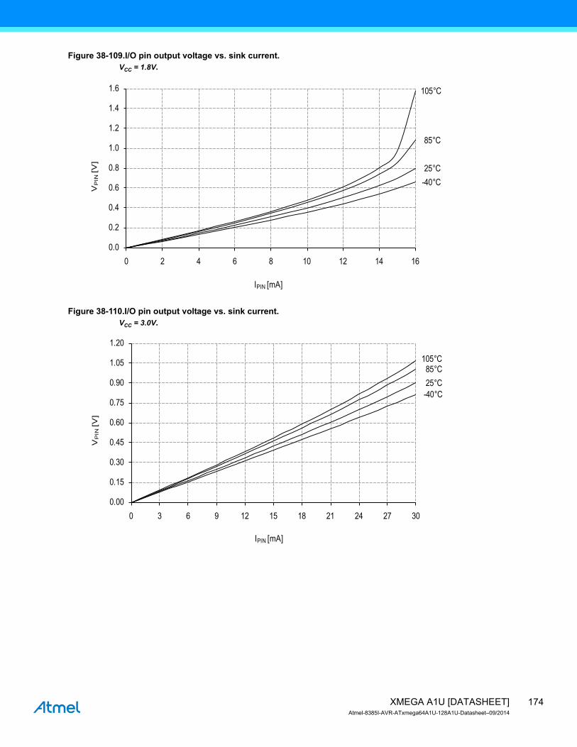
174XMEGA A1U [DATASHEET]Atmel-8385I-AVR-ATxmega64A1U-128A1U-Datasheet–09/2014
Figure 38-109.I/O pin output voltage vs. sink current.VCC = 1.8V.
Figure 38-110.I/O pin output voltage vs. sink current.VCC = 3.0V.
105 °C
85 °C
25 °C-40 °C
0.0
0.2
0.4
0.6
0.8
1.0
1.2
1.4
1.6
0 2 4 6 8 10 12 14 16
VP
IN[V
]
IPIN [mA]
105 °C85 °C25 °C-40 °C
0.00
0.15
0.30
0.45
0.60
0.75
0.90
1.05
1.20
0 3 6 9 12 15 18 21 24 27 30
VP
IN[V
]
IPIN [mA]
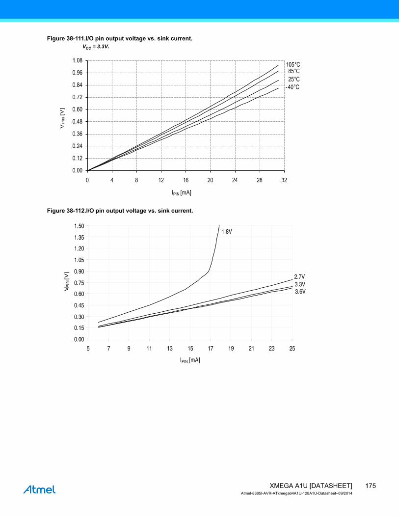
175XMEGA A1U [DATASHEET]Atmel-8385I-AVR-ATxmega64A1U-128A1U-Datasheet–09/2014
Figure 38-111.I/O pin output voltage vs. sink current.VCC = 3.3V.
Figure 38-112.I/O pin output voltage vs. sink current.
105 °C85 °C25 °C
-40 °C
0.00
0.12
0.24
0.36
0.48
0.60
0.72
0.84
0.96
1.08
0 4 8 12 16 20 24 28 32
VP
IN[V
]
IPIN [mA]
3.6V3.3V2.7V
0.00
0.15
0.30
0.45
0.60
0.75
0.90
1.05
1.20
1.35
1.50
5 7 9 11 13 15 17 19 21 23 25
IPIN [mA]
VP
IN [
V]
1.8V
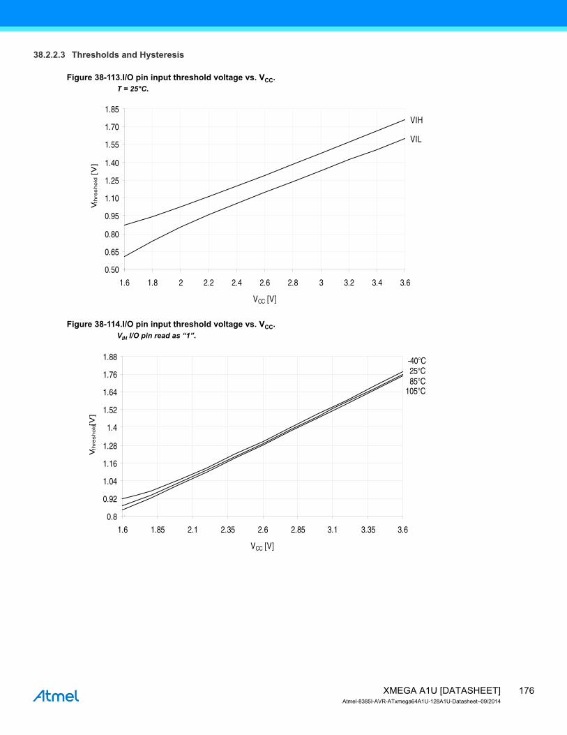
176XMEGA A1U [DATASHEET]Atmel-8385I-AVR-ATxmega64A1U-128A1U-Datasheet–09/2014
38.2.2.3 Thresholds and Hysteresis
Figure 38-113.I/O pin input threshold voltage vs. VCC.T = 25°C.
Figure 38-114.I/O pin input threshold voltage vs. VCC.VIH I/O pin read as “1”.
VIL
VIH
0.50
0.65
0.80
0.95
1.10
1.25
1.40
1.55
1.70
1.85
1.6 1.8 2 2.2 2.4 2.6 2.8 3 3.2 3.4 3.6
VCC [V]
Vth
resh
old [
V]
85°C25°C-40°C
0.8
0.92
1.04
1.16
1.28
1.4
1.52
1.64
1.76
1.88
1.6 1.85 2.1 2.35 2.6 2.85 3.1 3.35 3.6
VCC [V]
Vth
resh
old [
V]
105°C

177XMEGA A1U [DATASHEET]Atmel-8385I-AVR-ATxmega64A1U-128A1U-Datasheet–09/2014
Figure 38-115.I/O pin input threshold voltage vs. VCC.VIL I/O pin read as “0”.
Figure 38-116.I/O pin input hysteresis vs. VCC.
105 °C85 °C25 °C
-40 °C
0.50
0.65
0.80
0.95
1.10
1.25
1.40
1.55
1.70
1.6 1.85 2.1 2.35 2.6 2.85 3.1 3.35 3.6
Vth
resh
old
[V]
VCC [V]
105 °C
85 °C
25 °C
-40 °C
0.12
0.15
0.18
0.21
0.24
0.27
0.3
0.33
0.36
1.6 1.8 2 2.2 2.4 2.6 2.8 3 3.2 3.4 3.6
Vth
resh
old
[V]
VCC [V]

178XMEGA A1U [DATASHEET]Atmel-8385I-AVR-ATxmega64A1U-128A1U-Datasheet–09/2014
38.2.3 ADC Characteristics
Figure 38-117.INL error vs. external VREF.T = 25°C, VCC = 3.6V, external reference.
Figure 38-118.INL error vs. sample rate.T = 25°C, VCC = 3.6V, VREF = 2.0V external.
Single-ended unsigned mode
Single-ended signed mode
Differential mode
INL [
LS
B]
VREF [V]
0.7
0.8
0.9
1
1.1
1.2
1.3
1.4
1.5
1.6
1 1.2 1.4 1.6 1.8 2 2.2 2.4 2.6 2.8 3
Single-ended Unsigned mode
Single-ended Signed mode
Differential mode
0.9
0.93
0.96
0.99
1.02
1.05
1.08
1.11
1.14
1.17
500 650 800 950 1100 1250 1400 1550 1700 1850 2000
ADC Sample rate [ksps]
INL
[LS
B]

179XMEGA A1U [DATASHEET]Atmel-8385I-AVR-ATxmega64A1U-128A1U-Datasheet–09/2014
Figure 38-119.INL error vs. input code
Figure 38-120.DNL error vs. external VREF.T = 25°C, VCC = 3.6V, external reference.
-2
-1.5
-1
-0.5
0
0.5
1
1.5
2
0 512 1024 1536 2048 2560 3072 3584 4096
ADC input code
INL
[LS
B]
Single-ended unsigned mode
Single-ended signed mode
Differential mode
DN
L [
LS
B]
VREF [V]
0.2
0.3
0.4
0.5
0.6
0.7
0.8
0.9
1
1.1
1.2
1.3
1 1.2 1.4 1.6 1.8 2 2.2 2.4 2.6 2.8 3
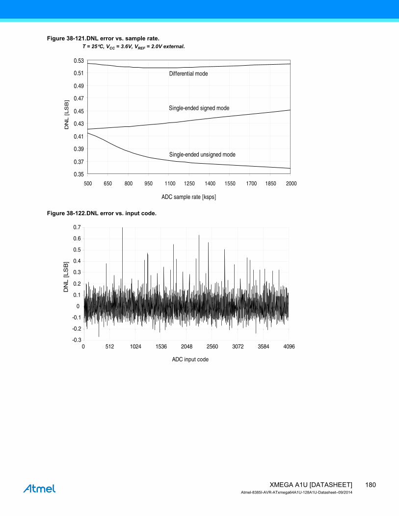
180XMEGA A1U [DATASHEET]Atmel-8385I-AVR-ATxmega64A1U-128A1U-Datasheet–09/2014
Figure 38-121.DNL error vs. sample rate.T = 25°C, VCC = 3.6V, VREF = 2.0V external.
Figure 38-122.DNL error vs. input code.
Single-ended unsigned mode
Single-ended signed mode
Differential mode
0.35
0.37
0.39
0.41
0.43
0.45
0.47
0.49
0.51
0.53
ADC sample rate [ksps]
DN
L [
LS
B]
500 650 800 950 1100 1250 1400 1550 1700 1850 2000
-0.3
-0.2
-0.1
0
0.1
0.2
0.3
0.4
0.5
0.6
0.7
0 512 1024 1536 2048 2560 3072 3584 4096
ADC input code
DN
L [
LS
B]
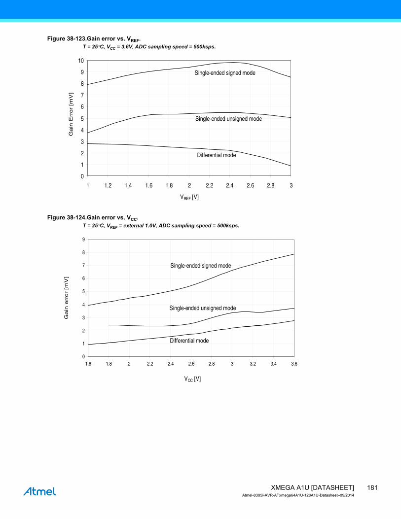
181XMEGA A1U [DATASHEET]Atmel-8385I-AVR-ATxmega64A1U-128A1U-Datasheet–09/2014
Figure 38-123.Gain error vs. VREF.T = 25°C, VCC = 3.6V, ADC sampling speed = 500ksps.
Figure 38-124.Gain error vs. VCC.T = 25°C, VREF = external 1.0V, ADC sampling speed = 500ksps.
Single-ended unsigned mode
Single-ended signed mode
Differential mode
0
1
2
3
4
5
6
7
8
9
10
1 1.2 1.4 1.6 1.8 2 2.2 2.4 2.6 2.8 3
VREF [V]
Gain
Err
or
[mV
]
0
1
2
3
4
5
6
7
8
9
1.6 1.8 2 2.2 2.4 2.6 2.8 3 3.2 3.4 3.6
Single-ended unsigned mode
Single-ended signed mode
Differential mode
VCC [V]
Gain
err
or
[mV
]

182XMEGA A1U [DATASHEET]Atmel-8385I-AVR-ATxmega64A1U-128A1U-Datasheet–09/2014
Figure 38-125.ADC Offset error vs. VREF.T = 25°C, VCC = 3.6V, ADC sampling speed = 500ksps.
Figure 38-126.Gain error vs. temperature.VCC = 3.0V, VREF = external 2.0V. TBD
Differential mode
-1.35
-1.3-1.25
-1.2
-1.15
-1.1-1.05
-1
-0.95
-0.9-0.85
-0.8
1 1.2 1.4 1.6 1.8 2 2.2 2.4 2.6 2.8 3
VREF [V]
Offset [m
V]
Single-ended Unsigned
Single-ended Signed
Differential
0
1
2
3
4
5
6
7
8
9
10
11
-45 -35 -25 -15 -5 5 15 25 35 45 55 65 75 85
Temperature [ºC]
Gain
Err
or
[mV
]
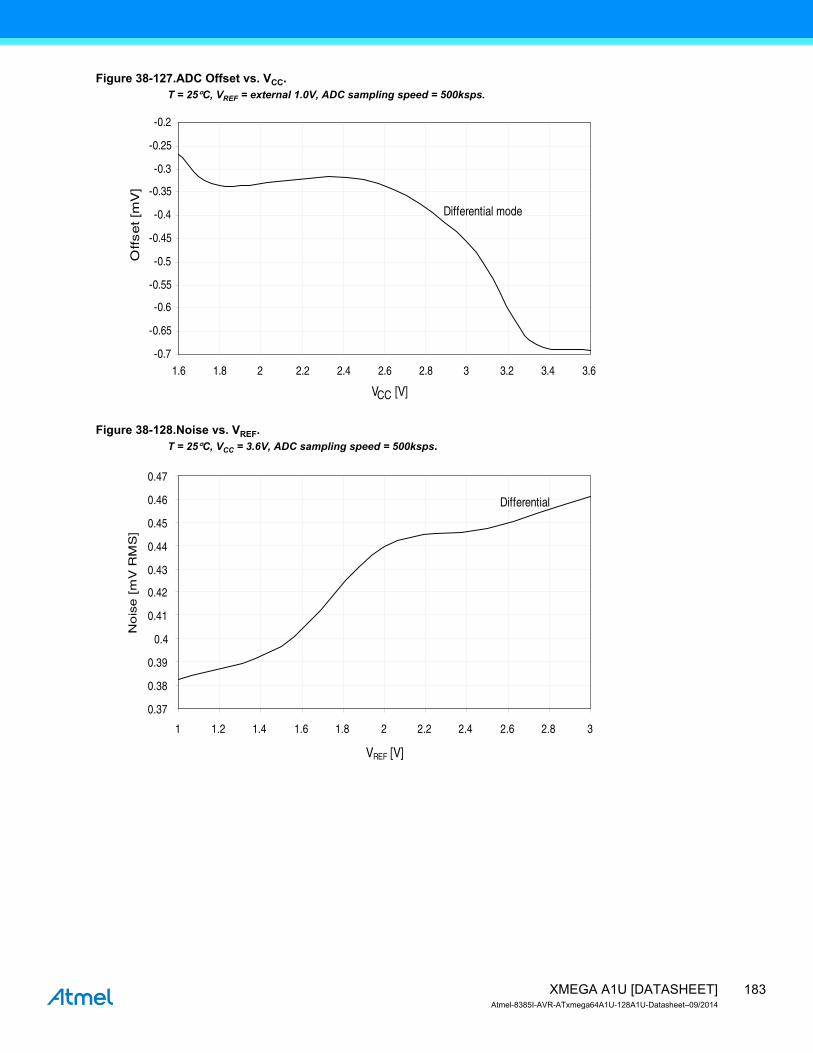
183XMEGA A1U [DATASHEET]Atmel-8385I-AVR-ATxmega64A1U-128A1U-Datasheet–09/2014
Figure 38-127.ADC Offset vs. VCC.T = 25°C, VREF = external 1.0V, ADC sampling speed = 500ksps.
Figure 38-128.Noise vs. VREF.T = 25°C, VCC = 3.6V, ADC sampling speed = 500ksps.
Differential mode
-0.7
-0.65
-0.6
-0.55
-0.5
-0.45
-0.4
-0.35
-0.3
-0.25
-0.2
1.6 1.8 2 2.2 2.4 2.6 2.8 3 3.2 3.4 3.6
VCC [V]
Offset [m
V]
Differential
0.37
0.38
0.39
0.4
0.41
0.42
0.43
0.44
0.45
0.46
0.47
1 1.2 1.4 1.6 1.8 2 2.2 2.4 2.6 2.8 3
VREF [V]
No
ise
[m
V R
MS
]
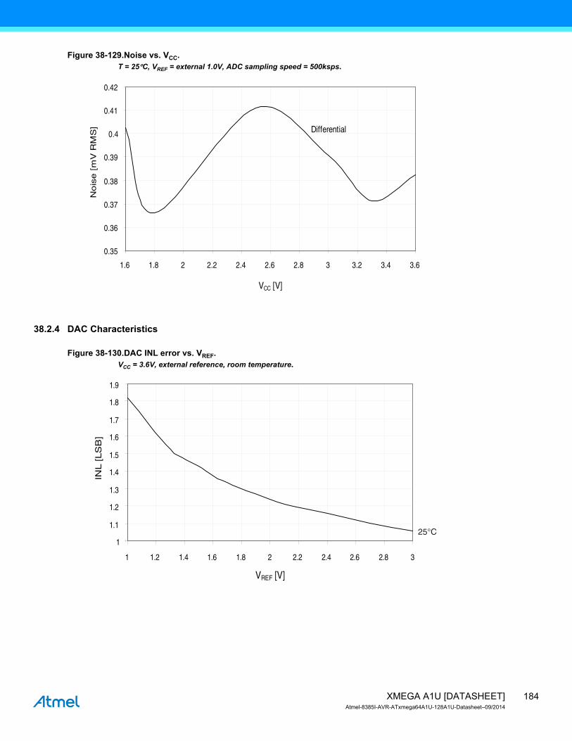
184XMEGA A1U [DATASHEET]Atmel-8385I-AVR-ATxmega64A1U-128A1U-Datasheet–09/2014
Figure 38-129.Noise vs. VCC.T = 25°C, VREF = external 1.0V, ADC sampling speed = 500ksps.
38.2.4 DAC Characteristics
Figure 38-130.DAC INL error vs. VREF.VCC = 3.6V, external reference, room temperature.
Differential
0.35
0.36
0.37
0.38
0.39
0.4
0.41
0.42
1.6 1.8 2 2.2 2.4 2.6 2.8 3 3.2 3.4 3.6
VCC [V]
No
ise
[m
V R
MS
]
1
1.1
1.2
1.3
1.4
1.5
1.6
1.7
1.8
1.9
1 1.2 1.4 1.6 1.8 2 2.2 2.4 2.6 2.8 3
VREF [V]
INL [LS
B]
25°C
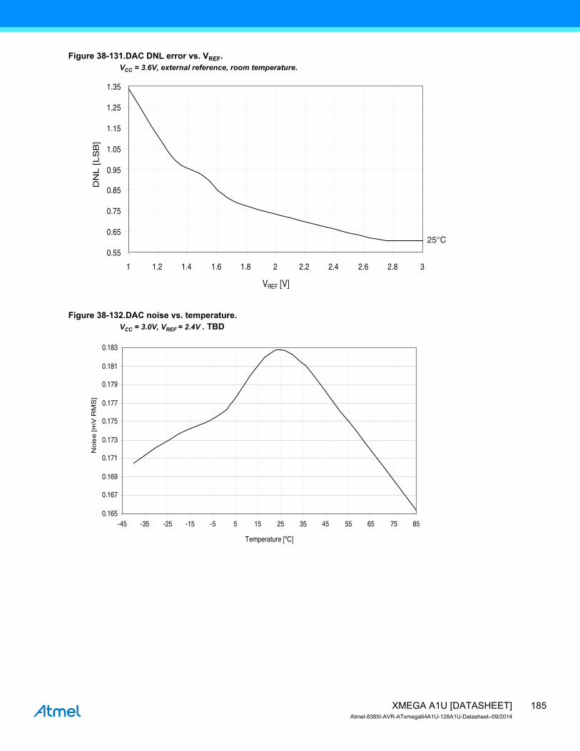
185XMEGA A1U [DATASHEET]Atmel-8385I-AVR-ATxmega64A1U-128A1U-Datasheet–09/2014
Figure 38-131.DAC DNL error vs. VREF.VCC = 3.6V, external reference, room temperature.
Figure 38-132.DAC noise vs. temperature.VCC = 3.0V, VREF = 2.4V . TBD
0.55
0.65
0.75
0.85
0.95
1.05
1.15
1.25
1.35
1 1.2 1.4 1.6 1.8 2 2.2 2.4 2.6 2.8 3
VREF [V]
DN
L [
LS
B]
25°C
0.165
0.167
0.169
0.171
0.173
0.175
0.177
0.179
0.181
0.183
-45 -35 -25 -15 -5 5 15 25 35 45 55 65 75 85
Temperature [ºC]
Nois
e [m
V R
MS
]
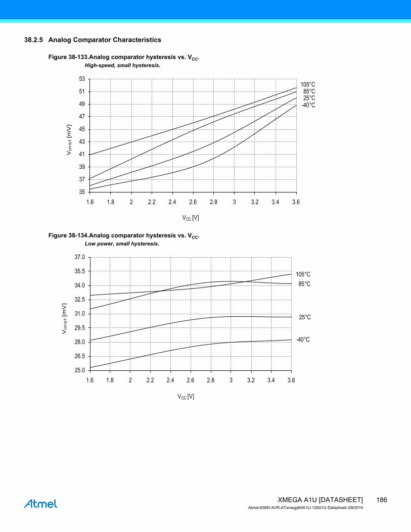
186XMEGA A1U [DATASHEET]Atmel-8385I-AVR-ATxmega64A1U-128A1U-Datasheet–09/2014
38.2.5 Analog Comparator Characteristics
Figure 38-133.Analog comparator hysteresis vs. VCC.High-speed, small hysteresis.
Figure 38-134.Analog comparator hysteresis vs. VCC.Low power, small hysteresis.
105 C85 °C25 °C
-40 °C
35
37
39
41
43
45
47
49
51
53
1.6 1.8 2 2.2 2.4 2.6 2.8 3 3.2 3.4 3.6
VH
YS
T[m
V]
VCC [V]
°
105 °C85 °C
25 °C
-40 °C
25.0
26.5
28.0
29.5
31.0
32.5
34.0
35.5
37.0
1.6 1.8 2 2.2 2.4 2.6 2.8 3 3.2 3.4 3.6
VH
YS
T[m
V]
VCC [V]
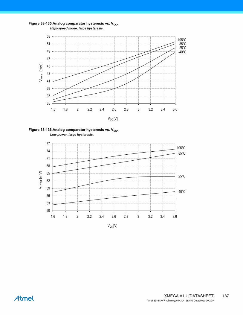
187XMEGA A1U [DATASHEET]Atmel-8385I-AVR-ATxmega64A1U-128A1U-Datasheet–09/2014
Figure 38-135.Analog comparator hysteresis vs. VCC.High-speed mode, large hysteresis.
Figure 38-136.Analog comparator hysteresis vs. VCC.Low power, large hysteresis.
105 C85 °C25 °C
-40 °C
35
37
39
41
43
45
47
49
51
53
1.6 1.8 2 2.2 2.4 2.6 2.8 3 3.2 3.4 3.6
VH
YS
T[m
V]
VCC [V]
°
105 °C85 °C
25 °C
-40 °C
50
53
56
59
62
65
68
71
74
77
1.6 1.8 2 2.2 2.4 2.6 2.8 3 3.2 3.4 3.6
VH
YS
T[m
V]
VCC [V]
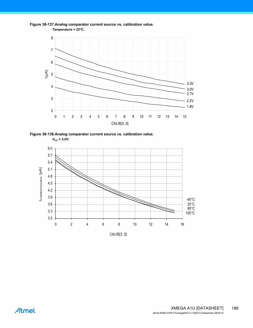
188XMEGA A1U [DATASHEET]Atmel-8385I-AVR-ATxmega64A1U-128A1U-Datasheet–09/2014
Figure 38-137.Analog comparator current source vs. calibration value.Temperature = 25°C.
Figure 38-138.Analog comparator current source vs. calibration value.VCC = 3.0V.
3.3V3.0V2.7V
2.2V1.8V
2
3
4
5
6
7
8
0 1 2 3 4 5 6 7 8 9 10 11 12 13 14 15
CALIB[3..0]
I [µ
A]
105 °C85 °C25 °C
-40°C
3.0
3.3
3.6
3.9
4.2
4.5
4.8
5.1
5.4
5.7
6.0
0 2 4 6 8 10 12 14 16
I CU
RR
EN
TSO
UR
CE
[µA
]
CALIB[3..0]
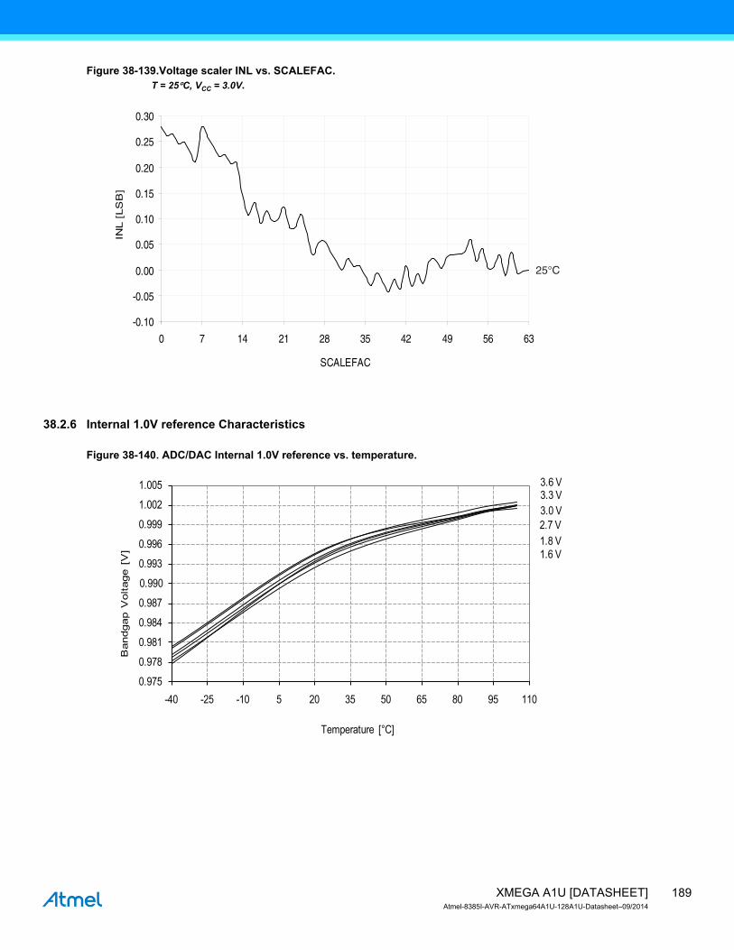
189XMEGA A1U [DATASHEET]Atmel-8385I-AVR-ATxmega64A1U-128A1U-Datasheet–09/2014
Figure 38-139.Voltage scaler INL vs. SCALEFAC.T = 25°C, VCC = 3.0V.
38.2.6 Internal 1.0V reference Characteristics
Figure 38-140. ADC/DAC Internal 1.0V reference vs. temperature.
-0.10
-0.05
0.00
0.05
0.10
0.15
0.20
0.25
0.30
0 7 14 21 28 35 42 49 56 63
SCALEFAC
INL [
LS
B]
25°C
3.6 V3.3 V3.0 V2.7 V1.8 V1.6 V
0.9750.9780.9810.9840.9870.9900.9930.9960.9991.0021.005
-40 -25 -10 5 20 35 50 65 80 95 110
Ban
dgap
Vol
tage
[V
]
Temperature [°C]
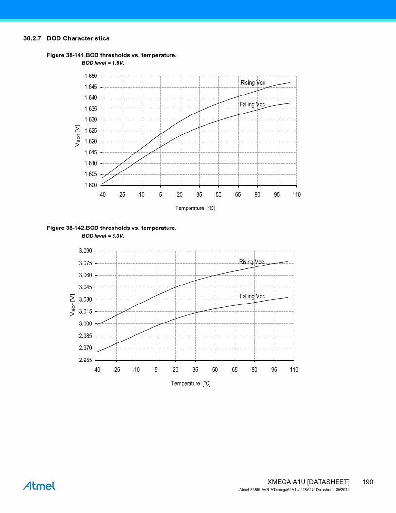
190XMEGA A1U [DATASHEET]Atmel-8385I-AVR-ATxmega64A1U-128A1U-Datasheet–09/2014
38.2.7 BOD Characteristics
Figure 38-141.BOD thresholds vs. temperature.BOD level = 1.6V.
Figure 38-142.BOD thresholds vs. temperature.BOD level = 3.0V.
Rising Vcc
Falling Vcc
1.600
1.605
1.610
1.615
1.620
1.625
1.630
1.635
1.640
1.645
1.650
-40 -25 -10 5 20 35 50 65 80 95 110
VB
OT
[V]
Temperature [°C]
Rising Vcc
Falling Vcc
2.955
2.970
2.985
3.000
3.015
3.030
3.045
3.060
3.075
3.090
-40 -25 -10 5 20 35 50 65 80 95 110
VB
OT
[V]
Temperature [°C]

191XMEGA A1U [DATASHEET]Atmel-8385I-AVR-ATxmega64A1U-128A1U-Datasheet–09/2014
38.2.8 External Reset Characteristics
Figure 38-143.Minimum Reset pin pulse width vs. VCC.
Figure 38-144.Reset pin pull-up resistor current vs. reset pin voltage.VCC = 1.8V.
105°C
85°C
25°C-40°C
60
68
76
84
92
100
108
116
124
1.6 1.8 2 2.2 2.4 2.6 2.8 3 3.2 3.4 3.6
t RS
T[n
s]
VCC [V]
105°C85°C25°C
-40°C
0
10
20
30
40
50
60
70
80
0 0.2 0.4 0.6 0.8 1 1.2 1.4 1.6 1.8
I RE
SE
T[µ
A]
VRESET [V]

192XMEGA A1U [DATASHEET]Atmel-8385I-AVR-ATxmega64A1U-128A1U-Datasheet–09/2014
Figure 38-145.Reset pin pull-up resistor current vs. reset pin voltage.VCC = 3.0V.
Figure 38-146.Reset pin pull-up resistor current vs. reset pin voltage.VCC = 3.3V.
0
15
30
45
60
75
90
105
120
135
0 0.3 0.6 0.9 1.2 1.5 1.8 2.1 2.4 2.7 3
I RE
SE
T[µ
A]
VRESET [V]
105°C85°C25°C
-40°C
0
20
40
60
80
100
120
140
160
0.00 0.35 0.70 1.05 1.40 1.75 2.10 2.45 2.80 3.15 3.50
I RE
SE
T[µ
A]
VRESET [V]
105°C85°C25°C
-40°C

193XMEGA A1U [DATASHEET]Atmel-8385I-AVR-ATxmega64A1U-128A1U-Datasheet–09/2014
Figure 38-147.Reset pin input threshold voltage vs. VCC.VIH - Reset pin read as “1”.
Figure 38-148.Reset pin input threshold voltage vs. VCC.VIL - Reset pin read as “0”.
1.00
1.15
1.30
1.45
1.60
1.75
1.90
2.05
2.20
1.6 1.8 2 2.2 2.4 2.6 2.8 3 3.2 3.4 3.6
Vth
resh
old
[V]
VCC [V]
105°C85°C25°C
-40°C
0.50
0.65
0.80
0.95
1.10
1.25
1.40
1.55
1.70
1.6 1.8 2 2.2 2.4 2.6 2.8 3 3.2 3.4 3.6
Vth
resh
old
[V]
VCC [V]
105°C85°C25°C
-40°C
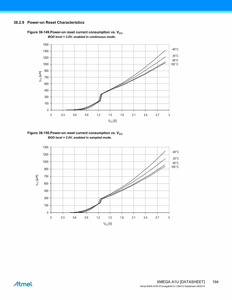
194XMEGA A1U [DATASHEET]Atmel-8385I-AVR-ATxmega64A1U-128A1U-Datasheet–09/2014
38.2.9 Power-on Reset Characteristics
Figure 38-149.Power-on reset current consumption vs. VCC.BOD level = 3.0V, enabled in continuous mode.
Figure 38-150.Power-on reset current consumption vs. VCC.BOD level = 3.0V, enabled in sampled mode.
105°C85°C25°C
-40°C
0
150
300
450
600
750
900
1050
1200
1350
1500
0 0.3 0.6 0.9 1.2 1.5 1.8 2.1 2.4 2.7 3
I CC
[µA
]
VCC [V]
0
150
300
450
600
750
900
1050
1200
1350
0 0.3 0.6 0.9 1.2 1.5 1.8 2.1 2.4 2.7 3
I CC
[µA
]
VCC [V]
105°C85°C25°C
-40°C

195XMEGA A1U [DATASHEET]Atmel-8385I-AVR-ATxmega64A1U-128A1U-Datasheet–09/2014
38.2.10 Oscillator Characteristics
38.2.10.1 Ultra Low-Power internal oscillator
Figure 38-151.Ultra Low-Power internal oscillator frequency vs. temperature.
38.2.10.2 32.768kHz Internal Oscillator
Figure 38-152. 32.768kHz internal oscillator frequency vs. temperature.
3.3 V3.0 V2.7 V2.2 V1.8 V26.8
27.2
27.6
28.0
28.4
28.8
29.2
29.6
30.0
-40 -25 -10 5 20 35 50 65 80 95 110
Fre
quen
cy [
kHz]
Temperature [°C]
3.3 V3.0 V
2.7 V2.2 V1.8 V
32.500
32.550
32.600
32.650
32.700
32.750
32.800
32.850
32.900
-40 -25 -10 5 20 35 50 65 80 95 110
Fre
quen
cy [
kHz]
Temperature [°C]
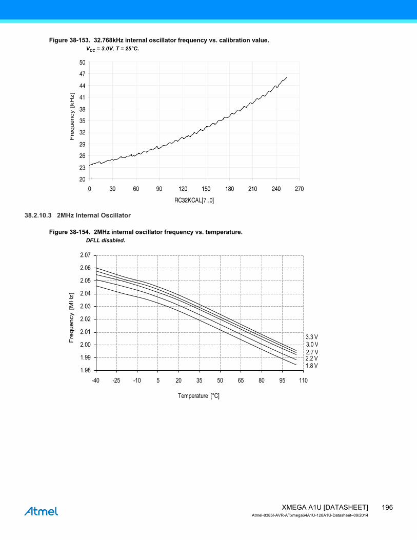
196XMEGA A1U [DATASHEET]Atmel-8385I-AVR-ATxmega64A1U-128A1U-Datasheet–09/2014
Figure 38-153. 32.768kHz internal oscillator frequency vs. calibration value.VCC = 3.0V, T = 25°C.
38.2.10.3 2MHz Internal Oscillator
Figure 38-154. 2MHz internal oscillator frequency vs. temperature.DFLL disabled.
20
23
26
29
32
35
38
41
44
47
50
0 30 60 90 120 150 180 210 240 270
RC32KCAL[7..0]
Fre
quency [
kH
z]
3.3 V3.0 V2.7 V2.2 V1.8 V
1.98
1.99
2.00
2.01
2.02
2.03
2.04
2.05
2.06
2.07
-40 -25 -10 5 20 35 50 65 80 95 110
Fre
quen
cy [
MH
z]
Temperature [°C]
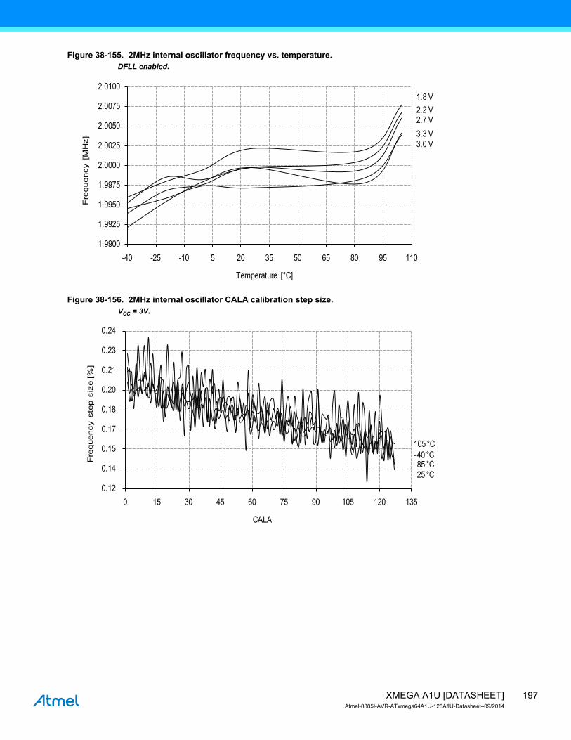
197XMEGA A1U [DATASHEET]Atmel-8385I-AVR-ATxmega64A1U-128A1U-Datasheet–09/2014
Figure 38-155. 2MHz internal oscillator frequency vs. temperature.DFLL enabled.
Figure 38-156. 2MHz internal oscillator CALA calibration step size.VCC = 3V.
3.3 V3.0 V
2.7 V2.2 V1.8 V
1.9900
1.9925
1.9950
1.9975
2.0000
2.0025
2.0050
2.0075
2.0100
-40 -25 -10 5 20 35 50 65 80 95 110
Fre
quen
cy [
MH
z]
Temperature [°C]
105 °C
85 °C25 °C
-40 °C
0.12
0.14
0.15
0.17
0.18
0.20
0.21
0.23
0.24
0 15 30 45 60 75 90 105 120 135
Fre
quen
cy s
tep
size
[%]
CALA

198XMEGA A1U [DATASHEET]Atmel-8385I-AVR-ATxmega64A1U-128A1U-Datasheet–09/2014
38.2.10.4 32MHz Internal Oscillator
Figure 38-157. 32MHz internal oscillator frequency vs. temperature.DFLL disabled.
Figure 38-158. 32MHz internal oscillator frequency vs. temperature.DFLL enabled, from the 32.768kHz internal oscillator.
3.3 V3.0 V2.7 V2.2 V1.8 V31.2
31.5
31.8
32.1
32.4
32.7
33.0
33.3
33.6
33.9
34.2
-40 -25 -10 5 20 35 50 65 80 95 110
Fre
quen
cy [
MH
z]
Temperature [°C]
3.3 V
3.0 V 2.7 V
2.2 V1.8 V
31.75
31.80
31.85
31.90
31.95
32.00
32.05
32.10
-40 -25 -10 5 20 35 50 65 80 95 110
Fre
quen
cy [
MH
z]
Temperature [°C]

199XMEGA A1U [DATASHEET]Atmel-8385I-AVR-ATxmega64A1U-128A1U-Datasheet–09/2014
Figure 38-159. 32MHz internal oscillator CALA calibration step size.VCC = 3.0V.
Figure 38-160. 32MHz internal oscillator frequency vs. CALB calibration value.VCC = 3.0V, DFLL disabled.
105 °C85°C
25 °C-40 °C
0.10
0.12
0.14
0.16
0.18
0.20
0.22
0.24
0.26
0.28
0.30
0 15 30 45 60 75 90 105 120 135
Fre
quen
cy S
tep
size
[%]
CALA
105 °C85 °C25 °C
-40 °C
25
30
35
40
45
50
55
60
65
70
75
0 8 16 24 32 40 48 56 64
Fre
quen
cy [
MH
z]
CALB
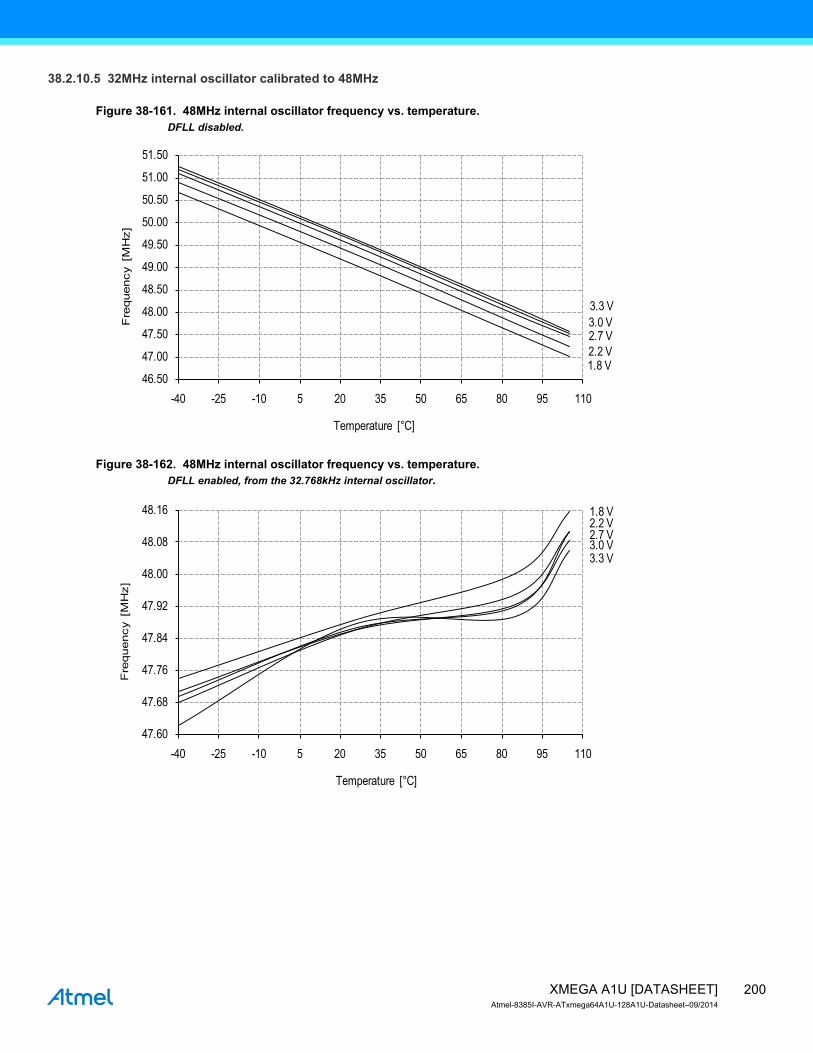
200XMEGA A1U [DATASHEET]Atmel-8385I-AVR-ATxmega64A1U-128A1U-Datasheet–09/2014
38.2.10.5 32MHz internal oscillator calibrated to 48MHz
Figure 38-161. 48MHz internal oscillator frequency vs. temperature.DFLL disabled.
Figure 38-162. 48MHz internal oscillator frequency vs. temperature.DFLL enabled, from the 32.768kHz internal oscillator.
3.3 V3.0 V2.7 V2.2 V1.8 V
46.50
47.00
47.50
48.00
48.50
49.00
49.50
50.00
50.50
51.00
51.50
-40 -25 -10 5 20 35 50 65 80 95 110
Fre
quen
cy [
MH
z]
Temperature [°C]
3.3 V3.0 V2.7 V2.2 V1.8 V
47.60
47.68
47.76
47.84
47.92
48.00
48.08
48.16
-40 -25 -10 5 20 35 50 65 80 95 110
Fre
quen
cy [
MH
z]
Temperature [°C]
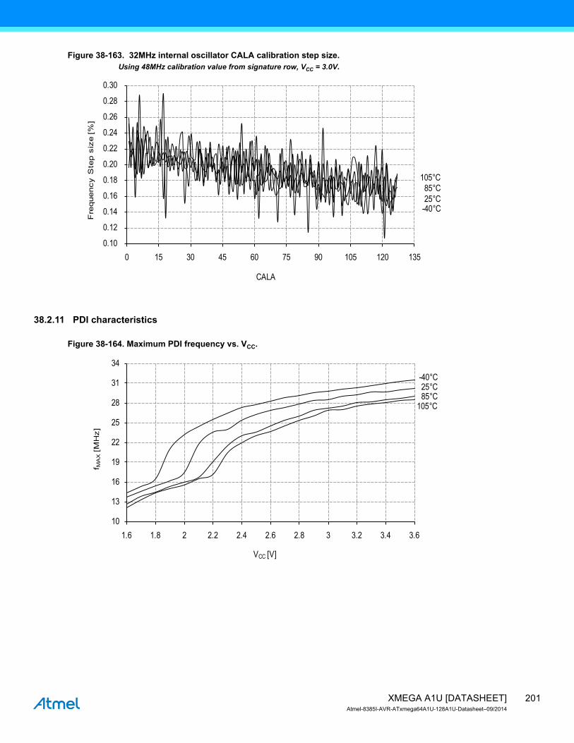
201XMEGA A1U [DATASHEET]Atmel-8385I-AVR-ATxmega64A1U-128A1U-Datasheet–09/2014
Figure 38-163. 32MHz internal oscillator CALA calibration step size.Using 48MHz calibration value from signature row, VCC = 3.0V.
38.2.11 PDI characteristics
Figure 38-164. Maximum PDI frequency vs. VCC.
105 °C85 °C25 °C
-40 °C
0.10
0.12
0.14
0.16
0.18
0.20
0.22
0.24
0.26
0.28
0.30
0 15 30 45 60 75 90 105 120 135
Fre
quen
cy S
tep
size
[%]
CALA
105 °C85 °C25 °C
-40 °C
10
13
16
19
22
25
28
31
34
1.6 1.8 2 2.2 2.4 2.6 2.8 3 3.2 3.4 3.6
f MA
X[M
Hz]
VCC [V]
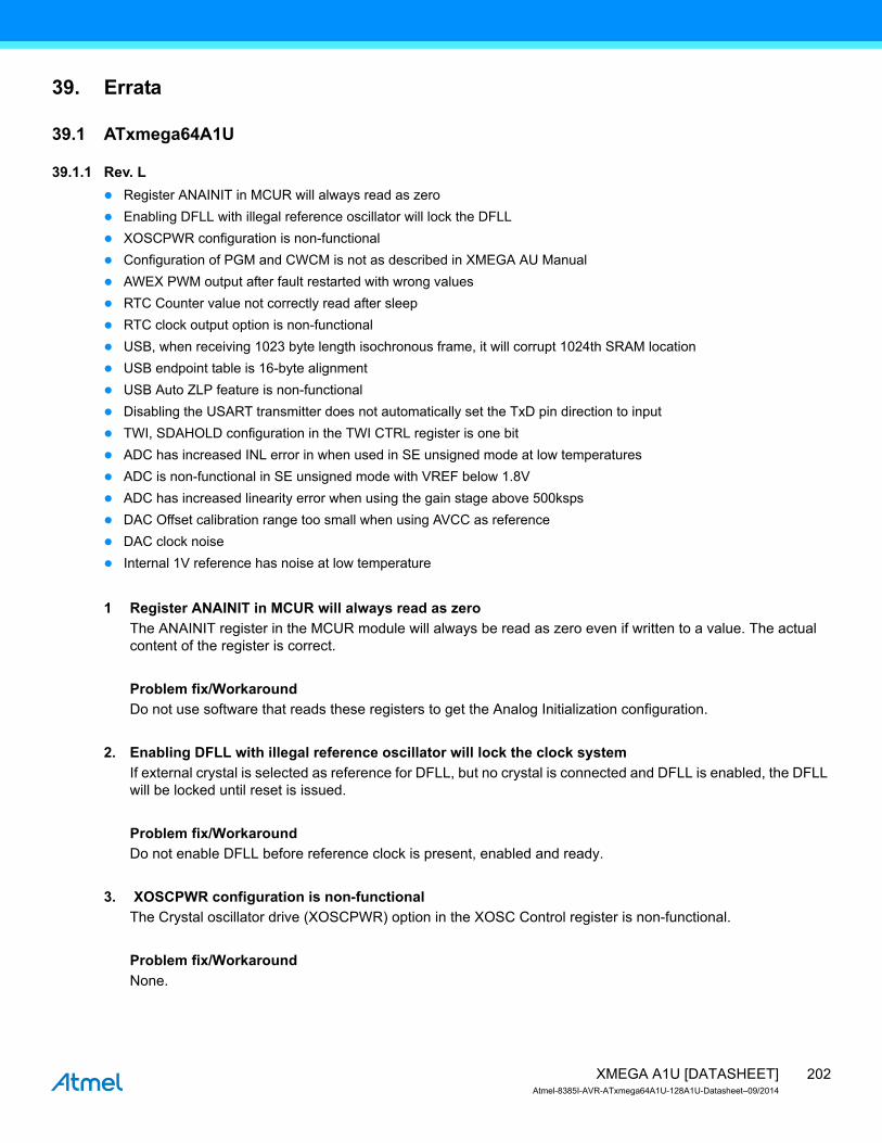
202XMEGA A1U [DATASHEET]Atmel-8385I-AVR-ATxmega64A1U-128A1U-Datasheet–09/2014
39. Errata
39.1 ATxmega64A1U
39.1.1 Rev. Lz Register ANAINIT in MCUR will always read as zeroz Enabling DFLL with illegal reference oscillator will lock the DFLLz XOSCPWR configuration is non-functionalz Configuration of PGM and CWCM is not as described in XMEGA AU Manualz AWEX PWM output after fault restarted with wrong valuesz RTC Counter value not correctly read after sleepz RTC clock output option is non-functionalz USB, when receiving 1023 byte length isochronous frame, it will corrupt 1024th SRAM locationz USB endpoint table is 16-byte alignmentz USB Auto ZLP feature is non-functionalz Disabling the USART transmitter does not automatically set the TxD pin direction to inputz TWI, SDAHOLD configuration in the TWI CTRL register is one bitz ADC has increased INL error in when used in SE unsigned mode at low temperaturesz ADC is non-functional in SE unsigned mode with VREF below 1.8Vz ADC has increased linearity error when using the gain stage above 500kspsz DAC Offset calibration range too small when using AVCC as referencez DAC clock noise z Internal 1V reference has noise at low temperature
1 Register ANAINIT in MCUR will always read as zeroThe ANAINIT register in the MCUR module will always be read as zero even if written to a value. The actual content of the register is correct.
Problem fix/WorkaroundDo not use software that reads these registers to get the Analog Initialization configuration.
2. Enabling DFLL with illegal reference oscillator will lock the clock systemIf external crystal is selected as reference for DFLL, but no crystal is connected and DFLL is enabled, the DFLL will be locked until reset is issued.
Problem fix/WorkaroundDo not enable DFLL before reference clock is present, enabled and ready.
3. XOSCPWR configuration is non-functionalThe Crystal oscillator drive (XOSCPWR) option in the XOSC Control register is non-functional.
Problem fix/WorkaroundNone.
203XMEGA A1U [DATASHEET]Atmel-8385I-AVR-ATxmega64A1U-128A1U-Datasheet–09/2014
4. Configuration of PGM and CWCM is not as described in XMEGA AU ManualConfiguration of common waveform channel mode (CWCM) and pattern generation mode (PGM), is not as described in the XMEGA AU manual.
Problem fix/WorkaroundConfigure PWM and CWCM according to the Table 39-1 on page 203.
Table 39-1. PWM and CWCM configuration.
5. AWEX PWM output after fault restarted with wrong valuesWhen recovering from fault state, the PWM output will drive wrong values to the port for up to two CLKPER + one CLKPER4 cycles.
Problem fix/WorkaroundThe following seqence can be used in Latched Mode:
a. Disable DTI outputs (Write DTICCxEN to 0)b. Clear fault flagc. Wait for Overflowd. Re-enable DTI (Write DTICCxEN to 1)e. Set pin direction to Output
This will remove the glitch, but the following period will be shorter. In Cycle-by-cycle mode the same procedure can be followed as long as the Pattern Generation Mode is not enabled.
For Pattern generation mode, there is no workaround.
6. RTC Counter value not correctly read after sleep If a real time counter (RTC) interrupt is used wake up the device from sleep, and bit 0 of RTC count register (CNT) has the same value as when the device entered sleep, CNT will not be read correctly during the first prescaled RTC clock cycle after wakeup. The value read will be the same as the value in the register was when entering sleep.
Problem fix/WorkaroundWait at least one prescaled RTC clock cycle before reading CNT.
7. RTC clock output option is non-functional The real time counter (RTC) as clock output option is non-functional, and setting the RTCOUT bit in the clock and event out register (CLKEVOUT ) will have no effect.
Problem fix/WorkaroundNone
PGM CWCM Description
0 0 PGM and CWCM disabled
0 1 PGM enabled
1 0 PGM and CWCM enabled
1 1 PGM enabled
204XMEGA A1U [DATASHEET]Atmel-8385I-AVR-ATxmega64A1U-128A1U-Datasheet–09/2014
8. USB, when receiving 1023Byte length isochronous frame, it will corrupt 1024th SRAM locationWhen USB is configured for isochronous operation and 1023Byte data payload size, the 1024th RAM location that is directly after the endpoint RAM buffer will be corrupted.
Problem fix/WorkaroundAllocate 1024bytes RAM buffer when using 1023 isochronous endpoint. This workaround is implemented in all USB software and source code delivered from Atmel in the AVR Software Framework.
9. USB endpoint table is 16-byte alignmentThe USB endpoint table uses 16-byte alignment, instead of 16-bit alignment.
Problem fix/WorkaroundAlign the endpoint configuration table pointer in SRAM to a 16-byte. This workaround is implemented in all USB software and source code delivered from Atmel in the AVR Software Framework.
10. USB Auto ZLP feature is non-functionalThe Auto ZLP feature is non-functional and can not be used.
Problem fix/WorkaroundNone.
11. Disabling the USART transmitter does not automatically set the TxD pin direction to inputIf the USART transmitter is idle with no frames to transmit, setting TXEN to zero will not automatically set the TxD pin direction to input.
Problem fix/WorkaroundThe TxD pin direction can be set to input using the Port pin direction to input using the port direction (DIR) reg-ister. When the port pin direction is input, it will be immediate and ongoing transmissions will be truncated.
12. TWI, SDAHOLD configuration in the TWI CTRL register is one bitThe SDAHOLD configuration in the TWI Control register (CTRL) is one bit. Due to this the SDA hold time can be configured for maximum ~50ns when enabled. Configuring for longer hold time will have no effect.
Problem fix/WorkaroundIf longer SDA hold time than 50nS is required it must be handled in software.
13. ADC has increased INL error in when used in SE unsigned mode at low temperaturesWhen the ADC is used on single ended (SE) unsigned mode, -INL error is increased up to +/- 5 LSB in temper-atures below -20C.
Problem fix/WorkaroundUse the ADC in single ended signed mode.
14. ADC is non-functional in SE unsigned mode with VREF below 1.8VWhen the ADC is used on single ended unsigned mode and VREF is below 1.8V, INL and DNL error is increased above +/- 10LSB, i.e. the ADC have missing codes under this condition.
205XMEGA A1U [DATASHEET]Atmel-8385I-AVR-ATxmega64A1U-128A1U-Datasheet–09/2014
Problem fix/WorkaroundUse the ADC in single ended signed mode.
15. ADC has increased linearity error when using the gain stage above 500kspsThe INL error for gain stage is increased to above 20LSB for sampling speed exceeding 500 ksps.
Problem fix/WorkaroundNone.
16. DAC Offset calibration range too small when using AVCC as referenceIf using AVCC as reference, the DAC offset calibration will not totally remove the offset error. Offset could be up to 100LSB after calibration.
Problem fix/WorkaroundOffset adjustment must be partly handled in software.
17. DAC clock noiseThe system clock is visible as clock noise on the output of the DAC. Peak to peak noise is in the range 0.7mV - 1.6mV at 2MHz and 0.05mV to 0.1mV at 32MHz. If external clock is used as system clock, the noise is up to three times higher.
Problem fix/WorkaroundAdd external low-pass filter to remove the noise.
18. Internal 1V reference has noise at low temperatureThe internal 1.0V reference for the ADC and DAC has increased noise at low temperatures. The noise can result in INL numbers up to +/- 20 LSB at temperatures below 0C.
Problem fix/WorkaroundFor the ADC, use oversampling to reduce noise. For the DAC use external filter to reduce the noise.
39.1.2 Rev. A – K
Not sampled.
206XMEGA A1U [DATASHEET]Atmel-8385I-AVR-ATxmega64A1U-128A1U-Datasheet–09/2014
39.2 ATxmega128A1U
39.2.1 Rev. Lz Register ANAINIT in MCUR will always read as zeroz Enabling DFLL with illegal reference oscillator will lock the DFLLz XOSCPWR configuration is non-functionalz Configuration of PGM and CWCM is not as described in XMEGA AU Manualz AWEX PWM output after fault restarted with wrong valuesz RTC Counter value not correctly read after sleepz RTC clock output option is non-functionalz USB, when receiving 1023 byte length isochronous frame, it will corrupt 1024th SRAM locationz USB endpoint table is 16-byte alignmentz USB Auto ZLP feature is non-functionalz Disabling the USART transmitter does not automatically set the TxD pin direction to inputz TWI, SDAHOLD configuration in the TWI CTRL register is one bitz ADC has increased INL error in when used in SE unsigned mode at low temperaturesz ADC is non-functional in SE unsigned mode with VREF below 1.8Vz ADC has increased linearity error when using the gain stage above 500kspsz DAC Offset calibration range too small when using AVCC as referencez DAC clock noise z Internal 1V reference has noise at low temperature
1 Register ANAINIT in MCUR will always read as zeroThe ANAINIT register in the MCUR module will always be read as zero even if written to a value. The actual content of the register is correct.
Problem fix/WorkaroundDo not use software that reads these registers to get the Analog Initialization configuration.
2. Enabling DFLL with illegal reference oscillator will lock the clock systemIf external crystal is selected as reference for DFLL, but no crystal is connected and DFLL is enabled, the DFLL will be locked until reset is issued.
Problem fix/WorkaroundDo not enable DFLL before reference clock is present, enabled and ready.
3. XOSCPWR configuration is non-functionalThe Crystal oscillator drive (XOSCPWR) option in the XOSC Control register is non-functional.
Problem fix/WorkaroundNone.
4. Configuration of PGM and CWCM is not as described in XMEGA AU ManualConfiguration of common waveform channel mode (CWCM) and pattern generation mode (PGM), is not as described in the XMEGA AU manual.
207XMEGA A1U [DATASHEET]Atmel-8385I-AVR-ATxmega64A1U-128A1U-Datasheet–09/2014
Problem fix/WorkaroundConfigure PWM and CWCM according to the Table 39-1 on page 203.
Table 39-2. PWM and CWCM configuration.
5. AWEX PWM output after fault restarted with wrong valuesWhen recovering from fault state, the PWM output will drive wrong values to the port for up to two CLKPER + one CLKPER4 cycles.
Problem fix/WorkaroundThe following seqence can be used in Latched Mode:
a. Disable DTI outputs (Write DTICCxEN to 0)b. Clear fault flagc. Wait for Overflowd. Re-enable DTI (Write DTICCxEN to 1)e. Set pin direction to Output
This will remove the glitch, but the following period will be shorter. In Cycle-by-cycle mode the same procedure can be followed as long as the Pattern Generation Mode is not enabled.
For Pattern generation mode, there is no workaround.
6. RTC Counter value not correctly read after sleep If a real time counter (RTC) interrupt is used wake up the device from sleep, and bit 0 of RTC count register (CNT) has the same value as when the device entered sleep, CNT will not be read correctly during the first prescaled RTC clock cycle after wakeup. The value read will be the same as the value in the register was when entering sleep.
Problem fix/WorkaroundWait at least one prescaled RTC clock cycle before reading CNT.
7. RTC clock output option is non-functional The real time counter (RTC) as clock output option is non-functional, and setting the RTCOUT bit in the clock and event out register (CLKEVOUT) will have no effect.
Problem fix/WorkaroundNone
8. USB, when receiving 1023Byte length isochronous frame, it will corrupt 1024th SRAM locationWhen USB is configured for isochronous operation and 1023Byte data payload size, the 1024th RAM location that is directly after the endpoint RAM buffer will be corrupted.
PGM CWCM Description
0 0 PGM and CWCM disabled
0 1 PGM enabled
1 0 PGM and CWCM enabled
1 1 PGM enabled
208XMEGA A1U [DATASHEET]Atmel-8385I-AVR-ATxmega64A1U-128A1U-Datasheet–09/2014
Problem fix/WorkaroundAllocate 1024bytes RAM buffer when using 1023 isochronous endpoint. This workaround is implemented in all USB software and source code delivered from Atmel in the AVR Software Framework.
9. USB endpoint table is 16-byte alignmentThe USB endpoint table uses 16-byte alignment, instead of 16-bit alignment.
Problem fix/WorkaroundAlign the endpoint configuration table pointer in SRAM to a 16-byte. This workaround is implemented in all USB software and source code delivered from Atmel in the AVR Software Framework.
10. USB Auto ZLP feature is non-functionalThe Auto ZLP feature is non-functional and can not be used.
Problem fix/WorkaroundNone.
11. Disabling the USART transmitter does not automatically set the TxD pin direction to inputIf the USART transmitter is idle with no frames to transmit, setting TXEN to zero will not automatically set the TxD pin direction to input.
Problem fix/WorkaroundThe TxD pin direction can be set to input using the Port pin direction to input using the port direction (DIR) reg-ister. When the port pin direction is input, it will be immediate and ongoing transmissions will be truncated.
12. TWI, SDAHOLD configuration in the TWI CTRL register is one bitThe SDAHOLD configuration in the TWI Control register (CTRL) is one bit. Due to this the SDA hold time can be configured for maximum ~50ns when enabled. Configuring for longer hold time will have no effect.
Problem fix/WorkaroundIf longer SDA hold time than 50nS is required it must be handled in software.
13. ADC has increased INL error in when used in SE unsigned mode at low temperaturesWhen the ADC is used on single ended (SE) unsigned mode, -INL error is increased up to +/- 5 LSB in temper-atures below -20C.
Problem fix/WorkaroundUse the ADC in single ended signed mode.
14. ADC is non-functional in SE unsigned mode with VREF below 1.8VWhen the ADC is used on single ended unsigned mode and VREF is below 1.8V, INL and DNL error is increased above +/- 10LSB, i.e. the ADC have missing codes under this condition.
Problem fix/WorkaroundUse the ADC in single ended signed mode.
209XMEGA A1U [DATASHEET]Atmel-8385I-AVR-ATxmega64A1U-128A1U-Datasheet–09/2014
15. ADC has increased linearity error when using the gain stage above 500kspsThe INL error for gain stage is increased to above 20LSB for sampling speed exceeding 500 ksps.
Problem fix/WorkaroundNone.
16. DAC Offset calibration range too small when using AVCC as referenceIf using AVCC as reference, the DAC offset calibration will not totally remove the offset error. Offset could be up to 100LSB after calibration.
Problem fix/WorkaroundOffset adjustment must be partly handled in software.
17. DAC clock noiseThe system clock is visible as clock noise on the output of the DAC. Peak to peak noise is in the range 0.7mV - 1.6mV at 2MHz and 0.05mV to 0.1mV at 32MHz. If external clock is used as system clock, the noise is up to three times higher.
Problem fix/WorkaroundAdd external low-pass filter to remove the noise.
18. Internal 1V reference has noise at low temperatureThe internal 1.0V reference for the ADC and DAC has increased noise at low temperatures. The noise can result in INL numbers up to +/- 20 LSB at temperatures below 0C.
Problem fix/WorkaroundFor the ADC, use oversampling to reduce noise. For the DAC use external filter to reduce the noise.
39.2.2 Rev. A – K
Not sampled.
210XMEGA A1U [DATASHEET]Atmel-8385I-AVR-ATxmega64A1U-128A1U-Datasheet–09/2014
40. Datasheet Revision HistoryPlease note that the referring page numbers in this section are referred to this document. The referring revision in this section are referring to the document revision.
40.1 8385I – 07/2014
40.2 8385H – 05/2014
40.3 8385G – 11/2013
40.4 8385F – 12/2012
40.5 8385E – 11/2012
1. Changed Vcc to AVcc in Section 29. “ADC – 12-bit Analog to Digital Converter” on page 49 and Section 31. “AC – Analog Comparator” on page 53.
2. Changed value for parameter tSU;DAT to “ns” in table Table 37-34 on page 96.
1. Updated “Ordering Information” on page 2. The ATxmega64A1U and ATxmega128A1U @ 105°C added.
2. Updated Table 37-4 on page 76 and Table 37-38 on page 99. Added Icc Power-down power consumption for T=105°C for all functions disabled and for WDT and sampled BOD enabled.
3. Updated Table 37-20 on page 85 and Table 37-54 on page 108. Updated all tables to include values for T=85°C and T=105°C. Removed T=55°C.
4. Updated the typical characteristics at 105°C in “ATxmega64A1U” on page 120 and “ATxmega128A1U” on page 161.
1. Updated note 2 in Port H - Alternate Functions in Table 33-7 on page 60.
1. Updated the typical characteristics at 105°C for “ATxmega128A1U” on page 161.
1. Updated the whole contents with an updated template (table tags and paragraph tags).
2. Updated the 100C1 package type on page 2. Ball pitch is 0.80mm instead of 0.88mm.
3. Updated Figure 2-1 on page 3. Pin 14 is VCC and not VDD.
4. Updated Table 7-2 on page 14. ATxmega64A1U has internal SRAM (4K). ATxmega128A1U has internal SRAM (8K).
5. Updated Figure 15-7 on page 33, “Input sensing system overview” .
6. Updated Figure 31-1 on page 54, “Analog comparator overview.”
211XMEGA A1U [DATASHEET]Atmel-8385I-AVR-ATxmega64A1U-128A1U-Datasheet–09/2014
40.6 8385D – 07/2012
40.7 8385C – 07/2012
40.8 8385B – 03/2012
40.9 8385A – 11/2011
7. Added electrical characterization for “ATxmega64A1U” on page 74.
8. Updated Table 37-29 on page 89 and Table 37-63 on page 112. Added ESR and start-up time parameters.
9. Added typical characteristics for “ATxmega64A1U” on page 120.
1. Updated Table 7-2 on page 15. Devices are respectively ATxmega64A1U and ATxmega128A1U.
1. Updated Table 7-1 on page 13. Device ID for ATxmega128A1U is 4C97. Device ID for ATxmega64A1U is 4E96.
2. Updated the package “100C2” on page 73. The ball rows are A-K (without I).
3. Updated the whole datasheet using the Atmel new updated datasheet template that includes Atmel new logo and new registered TM.
1. Added “Electrical Characteristics” on page 74.
2. Added “Typical Characteristics” on page 120.
3. Updated “Errata” on page 202.
4. Used Atmel new datasheet template that includes Atmel new addresses on the last page.
1. Initial revision.
iXMEGA A1U [DATASHEET]Atmel-8385I-AVR-ATxmega64A1U-128A1U-Datasheet–09/2014
Table of Contents
Features. . . . . . . . . . . . . . . . . . . . . . . . . . . . . . . . . . . . . . . . . . . . . . . . . . . . . . . . . . . . . . . . . 1
1. Ordering Information . . . . . . . . . . . . . . . . . . . . . . . . . . . . . . . . . . . . . . . . . . . . . . . . . . 2
2. Pinout/Block Diagram . . . . . . . . . . . . . . . . . . . . . . . . . . . . . . . . . . . . . . . . . . . . . . . . . 3
3. Overview . . . . . . . . . . . . . . . . . . . . . . . . . . . . . . . . . . . . . . . . . . . . . . . . . . . . . . . . . . . . 53.1 Block Diagram. . . . . . . . . . . . . . . . . . . . . . . . . . . . . . . . . . . . . . . . . . . . . . . . . . . . . . . . . . . . . . . . . . . 6
4. Resources . . . . . . . . . . . . . . . . . . . . . . . . . . . . . . . . . . . . . . . . . . . . . . . . . . . . . . . . . . . 74.1 Recommended reading. . . . . . . . . . . . . . . . . . . . . . . . . . . . . . . . . . . . . . . . . . . . . . . . . . . . . . . . . . . . 7
5. Capacitive touch sensing . . . . . . . . . . . . . . . . . . . . . . . . . . . . . . . . . . . . . . . . . . . . . . 7
6. AVR CPU . . . . . . . . . . . . . . . . . . . . . . . . . . . . . . . . . . . . . . . . . . . . . . . . . . . . . . . . . . . . 86.1 Features . . . . . . . . . . . . . . . . . . . . . . . . . . . . . . . . . . . . . . . . . . . . . . . . . . . . . . . . . . . . . . . . . . . . . . . 86.2 Overview . . . . . . . . . . . . . . . . . . . . . . . . . . . . . . . . . . . . . . . . . . . . . . . . . . . . . . . . . . . . . . . . . . . . . . . 86.3 Architectural Overview . . . . . . . . . . . . . . . . . . . . . . . . . . . . . . . . . . . . . . . . . . . . . . . . . . . . . . . . . . . . 86.4 ALU - Arithmetic Logic Unit . . . . . . . . . . . . . . . . . . . . . . . . . . . . . . . . . . . . . . . . . . . . . . . . . . . . . . . . . 96.5 Program Flow . . . . . . . . . . . . . . . . . . . . . . . . . . . . . . . . . . . . . . . . . . . . . . . . . . . . . . . . . . . . . . . . . . 106.6 Status Register . . . . . . . . . . . . . . . . . . . . . . . . . . . . . . . . . . . . . . . . . . . . . . . . . . . . . . . . . . . . . . . . . 106.7 Stack and Stack Pointer . . . . . . . . . . . . . . . . . . . . . . . . . . . . . . . . . . . . . . . . . . . . . . . . . . . . . . . . . . 106.8 Register File . . . . . . . . . . . . . . . . . . . . . . . . . . . . . . . . . . . . . . . . . . . . . . . . . . . . . . . . . . . . . . . . . . . 10
7. Memories . . . . . . . . . . . . . . . . . . . . . . . . . . . . . . . . . . . . . . . . . . . . . . . . . . . . . . . . . . 117.1 Features . . . . . . . . . . . . . . . . . . . . . . . . . . . . . . . . . . . . . . . . . . . . . . . . . . . . . . . . . . . . . . . . . . . . . . 117.2 Overview . . . . . . . . . . . . . . . . . . . . . . . . . . . . . . . . . . . . . . . . . . . . . . . . . . . . . . . . . . . . . . . . . . . . . . 117.3 Flash Program Memory . . . . . . . . . . . . . . . . . . . . . . . . . . . . . . . . . . . . . . . . . . . . . . . . . . . . . . . . . . 127.4 Fuses and Lock bits . . . . . . . . . . . . . . . . . . . . . . . . . . . . . . . . . . . . . . . . . . . . . . . . . . . . . . . . . . . . . 137.5 Data Memory . . . . . . . . . . . . . . . . . . . . . . . . . . . . . . . . . . . . . . . . . . . . . . . . . . . . . . . . . . . . . . . . . . 137.6 EEPROM . . . . . . . . . . . . . . . . . . . . . . . . . . . . . . . . . . . . . . . . . . . . . . . . . . . . . . . . . . . . . . . . . . . . . 147.7 I/O Memory . . . . . . . . . . . . . . . . . . . . . . . . . . . . . . . . . . . . . . . . . . . . . . . . . . . . . . . . . . . . . . . . . . . . 147.8 External Memory. . . . . . . . . . . . . . . . . . . . . . . . . . . . . . . . . . . . . . . . . . . . . . . . . . . . . . . . . . . . . . . . 147.9 Data Memory and Bus Arbitration. . . . . . . . . . . . . . . . . . . . . . . . . . . . . . . . . . . . . . . . . . . . . . . . . . . 147.10 Memory Timing . . . . . . . . . . . . . . . . . . . . . . . . . . . . . . . . . . . . . . . . . . . . . . . . . . . . . . . . . . . . . . . . . 157.11 Device ID and Revision. . . . . . . . . . . . . . . . . . . . . . . . . . . . . . . . . . . . . . . . . . . . . . . . . . . . . . . . . . . 157.12 I/O Memory Protection . . . . . . . . . . . . . . . . . . . . . . . . . . . . . . . . . . . . . . . . . . . . . . . . . . . . . . . . . . . 157.13 JTAG Disable . . . . . . . . . . . . . . . . . . . . . . . . . . . . . . . . . . . . . . . . . . . . . . . . . . . . . . . . . . . . . . . . . . 157.14 Flash and EEPROM Page Size . . . . . . . . . . . . . . . . . . . . . . . . . . . . . . . . . . . . . . . . . . . . . . . . . . . . 15
8. DMAC – Direct Memory Access Controller . . . . . . . . . . . . . . . . . . . . . . . . . . . . . . . 178.1 Features . . . . . . . . . . . . . . . . . . . . . . . . . . . . . . . . . . . . . . . . . . . . . . . . . . . . . . . . . . . . . . . . . . . . . . 178.2 Overview . . . . . . . . . . . . . . . . . . . . . . . . . . . . . . . . . . . . . . . . . . . . . . . . . . . . . . . . . . . . . . . . . . . . . . 17
9. Event System . . . . . . . . . . . . . . . . . . . . . . . . . . . . . . . . . . . . . . . . . . . . . . . . . . . . . . . 189.1 Features . . . . . . . . . . . . . . . . . . . . . . . . . . . . . . . . . . . . . . . . . . . . . . . . . . . . . . . . . . . . . . . . . . . . . . 189.2 Overview . . . . . . . . . . . . . . . . . . . . . . . . . . . . . . . . . . . . . . . . . . . . . . . . . . . . . . . . . . . . . . . . . . . . . . 18
10. System Clock and Clock options . . . . . . . . . . . . . . . . . . . . . . . . . . . . . . . . . . . . . . . 1910.1 Features . . . . . . . . . . . . . . . . . . . . . . . . . . . . . . . . . . . . . . . . . . . . . . . . . . . . . . . . . . . . . . . . . . . . . . 1910.2 Overview . . . . . . . . . . . . . . . . . . . . . . . . . . . . . . . . . . . . . . . . . . . . . . . . . . . . . . . . . . . . . . . . . . . . . . 19
iiXMEGA A1U [DATASHEET]Atmel-8385I-AVR-ATxmega64A1U-128A1U-Datasheet–09/2014
10.3 Clock Sources. . . . . . . . . . . . . . . . . . . . . . . . . . . . . . . . . . . . . . . . . . . . . . . . . . . . . . . . . . . . . . . . . . 20
11. Power Management and Sleep Modes . . . . . . . . . . . . . . . . . . . . . . . . . . . . . . . . . . . 2211.1 Features . . . . . . . . . . . . . . . . . . . . . . . . . . . . . . . . . . . . . . . . . . . . . . . . . . . . . . . . . . . . . . . . . . . . . . 2211.2 Overview . . . . . . . . . . . . . . . . . . . . . . . . . . . . . . . . . . . . . . . . . . . . . . . . . . . . . . . . . . . . . . . . . . . . . . 2211.3 Sleep Modes . . . . . . . . . . . . . . . . . . . . . . . . . . . . . . . . . . . . . . . . . . . . . . . . . . . . . . . . . . . . . . . . . . . 22
12. System Control and Reset . . . . . . . . . . . . . . . . . . . . . . . . . . . . . . . . . . . . . . . . . . . . 2412.1 Features . . . . . . . . . . . . . . . . . . . . . . . . . . . . . . . . . . . . . . . . . . . . . . . . . . . . . . . . . . . . . . . . . . . . . . 2412.2 Overview . . . . . . . . . . . . . . . . . . . . . . . . . . . . . . . . . . . . . . . . . . . . . . . . . . . . . . . . . . . . . . . . . . . . . . 2412.3 Reset Sequence . . . . . . . . . . . . . . . . . . . . . . . . . . . . . . . . . . . . . . . . . . . . . . . . . . . . . . . . . . . . . . . . 2412.4 Reset Sources . . . . . . . . . . . . . . . . . . . . . . . . . . . . . . . . . . . . . . . . . . . . . . . . . . . . . . . . . . . . . . . . . 24
13. WDT – Watchdog Timer . . . . . . . . . . . . . . . . . . . . . . . . . . . . . . . . . . . . . . . . . . . . . . . 2613.1 Features . . . . . . . . . . . . . . . . . . . . . . . . . . . . . . . . . . . . . . . . . . . . . . . . . . . . . . . . . . . . . . . . . . . . . . 2613.2 Overview . . . . . . . . . . . . . . . . . . . . . . . . . . . . . . . . . . . . . . . . . . . . . . . . . . . . . . . . . . . . . . . . . . . . . . 26
14. Interrupts and Programmable Multilevel Interrupt Controller . . . . . . . . . . . . . . . . 2714.1 Features . . . . . . . . . . . . . . . . . . . . . . . . . . . . . . . . . . . . . . . . . . . . . . . . . . . . . . . . . . . . . . . . . . . . . . 2714.2 Overview . . . . . . . . . . . . . . . . . . . . . . . . . . . . . . . . . . . . . . . . . . . . . . . . . . . . . . . . . . . . . . . . . . . . . . 2714.3 Interrupt vectors . . . . . . . . . . . . . . . . . . . . . . . . . . . . . . . . . . . . . . . . . . . . . . . . . . . . . . . . . . . . . . . . 27
15. I/O Ports . . . . . . . . . . . . . . . . . . . . . . . . . . . . . . . . . . . . . . . . . . . . . . . . . . . . . . . . . . . 3015.1 Features . . . . . . . . . . . . . . . . . . . . . . . . . . . . . . . . . . . . . . . . . . . . . . . . . . . . . . . . . . . . . . . . . . . . . . 3015.2 Overview . . . . . . . . . . . . . . . . . . . . . . . . . . . . . . . . . . . . . . . . . . . . . . . . . . . . . . . . . . . . . . . . . . . . . . 3015.3 Output Driver. . . . . . . . . . . . . . . . . . . . . . . . . . . . . . . . . . . . . . . . . . . . . . . . . . . . . . . . . . . . . . . . . . . 3115.4 Input sensing. . . . . . . . . . . . . . . . . . . . . . . . . . . . . . . . . . . . . . . . . . . . . . . . . . . . . . . . . . . . . . . . . . . 3315.5 Alternate Port Functions . . . . . . . . . . . . . . . . . . . . . . . . . . . . . . . . . . . . . . . . . . . . . . . . . . . . . . . . . . 33
16. TC0/1 – 16-bit Timer/Counter Type 0 and 1 . . . . . . . . . . . . . . . . . . . . . . . . . . . . . . . 3416.1 Features . . . . . . . . . . . . . . . . . . . . . . . . . . . . . . . . . . . . . . . . . . . . . . . . . . . . . . . . . . . . . . . . . . . . . . 3416.2 Overview . . . . . . . . . . . . . . . . . . . . . . . . . . . . . . . . . . . . . . . . . . . . . . . . . . . . . . . . . . . . . . . . . . . . . . 34
17. TC2 – Time/Counter Type 2 . . . . . . . . . . . . . . . . . . . . . . . . . . . . . . . . . . . . . . . . . . . . 3617.1 Features . . . . . . . . . . . . . . . . . . . . . . . . . . . . . . . . . . . . . . . . . . . . . . . . . . . . . . . . . . . . . . . . . . . . . . 3617.2 Overview . . . . . . . . . . . . . . . . . . . . . . . . . . . . . . . . . . . . . . . . . . . . . . . . . . . . . . . . . . . . . . . . . . . . . . 36
18. AWeX – Advanced Waveform Extension . . . . . . . . . . . . . . . . . . . . . . . . . . . . . . . . . 3718.1 Features . . . . . . . . . . . . . . . . . . . . . . . . . . . . . . . . . . . . . . . . . . . . . . . . . . . . . . . . . . . . . . . . . . . . . . 3718.2 Overview . . . . . . . . . . . . . . . . . . . . . . . . . . . . . . . . . . . . . . . . . . . . . . . . . . . . . . . . . . . . . . . . . . . . . . 37
19. Hi-Res – High Resolution Extension . . . . . . . . . . . . . . . . . . . . . . . . . . . . . . . . . . . . 3819.1 Features . . . . . . . . . . . . . . . . . . . . . . . . . . . . . . . . . . . . . . . . . . . . . . . . . . . . . . . . . . . . . . . . . . . . . . 3819.2 Overview . . . . . . . . . . . . . . . . . . . . . . . . . . . . . . . . . . . . . . . . . . . . . . . . . . . . . . . . . . . . . . . . . . . . . . 38
20. RTC – 16-bit Real-Time Counter . . . . . . . . . . . . . . . . . . . . . . . . . . . . . . . . . . . . . . . . 3920.1 Features . . . . . . . . . . . . . . . . . . . . . . . . . . . . . . . . . . . . . . . . . . . . . . . . . . . . . . . . . . . . . . . . . . . . . . 3920.2 Overview . . . . . . . . . . . . . . . . . . . . . . . . . . . . . . . . . . . . . . . . . . . . . . . . . . . . . . . . . . . . . . . . . . . . . . 39
21. USB – Universal Serial Bus Interface . . . . . . . . . . . . . . . . . . . . . . . . . . . . . . . . . . . . 4021.1 Features . . . . . . . . . . . . . . . . . . . . . . . . . . . . . . . . . . . . . . . . . . . . . . . . . . . . . . . . . . . . . . . . . . . . . . 4021.2 Overview . . . . . . . . . . . . . . . . . . . . . . . . . . . . . . . . . . . . . . . . . . . . . . . . . . . . . . . . . . . . . . . . . . . . . . 40
22. TWI – Two-Wire Interface . . . . . . . . . . . . . . . . . . . . . . . . . . . . . . . . . . . . . . . . . . . . . 42
iiiXMEGA A1U [DATASHEET]Atmel-8385I-AVR-ATxmega64A1U-128A1U-Datasheet–09/2014
22.1 Features . . . . . . . . . . . . . . . . . . . . . . . . . . . . . . . . . . . . . . . . . . . . . . . . . . . . . . . . . . . . . . . . . . . . . . 4222.2 Overview . . . . . . . . . . . . . . . . . . . . . . . . . . . . . . . . . . . . . . . . . . . . . . . . . . . . . . . . . . . . . . . . . . . . . . 42
23. SPI – Serial Peripheral Interface . . . . . . . . . . . . . . . . . . . . . . . . . . . . . . . . . . . . . . . . 4323.1 Features . . . . . . . . . . . . . . . . . . . . . . . . . . . . . . . . . . . . . . . . . . . . . . . . . . . . . . . . . . . . . . . . . . . . . . 4323.2 Overview . . . . . . . . . . . . . . . . . . . . . . . . . . . . . . . . . . . . . . . . . . . . . . . . . . . . . . . . . . . . . . . . . . . . . . 43
24. USART . . . . . . . . . . . . . . . . . . . . . . . . . . . . . . . . . . . . . . . . . . . . . . . . . . . . . . . . . . . . . 4424.1 Features . . . . . . . . . . . . . . . . . . . . . . . . . . . . . . . . . . . . . . . . . . . . . . . . . . . . . . . . . . . . . . . . . . . . . . 4424.2 Overview . . . . . . . . . . . . . . . . . . . . . . . . . . . . . . . . . . . . . . . . . . . . . . . . . . . . . . . . . . . . . . . . . . . . . . 44
25. IRCOM – IR Communication Module . . . . . . . . . . . . . . . . . . . . . . . . . . . . . . . . . . . . 4525.1 Features . . . . . . . . . . . . . . . . . . . . . . . . . . . . . . . . . . . . . . . . . . . . . . . . . . . . . . . . . . . . . . . . . . . . . . 4525.2 Overview . . . . . . . . . . . . . . . . . . . . . . . . . . . . . . . . . . . . . . . . . . . . . . . . . . . . . . . . . . . . . . . . . . . . . . 45
26. AES and DES Crypto Engine . . . . . . . . . . . . . . . . . . . . . . . . . . . . . . . . . . . . . . . . . . 4626.1 Features . . . . . . . . . . . . . . . . . . . . . . . . . . . . . . . . . . . . . . . . . . . . . . . . . . . . . . . . . . . . . . . . . . . . . . 4626.2 Overview . . . . . . . . . . . . . . . . . . . . . . . . . . . . . . . . . . . . . . . . . . . . . . . . . . . . . . . . . . . . . . . . . . . . . . 46
27. CRC – Cyclic Redundancy Check Generator . . . . . . . . . . . . . . . . . . . . . . . . . . . . . 4727.1 Features . . . . . . . . . . . . . . . . . . . . . . . . . . . . . . . . . . . . . . . . . . . . . . . . . . . . . . . . . . . . . . . . . . . . . . 4727.2 Overview . . . . . . . . . . . . . . . . . . . . . . . . . . . . . . . . . . . . . . . . . . . . . . . . . . . . . . . . . . . . . . . . . . . . . . 47
28. EBI – External Bus Interface . . . . . . . . . . . . . . . . . . . . . . . . . . . . . . . . . . . . . . . . . . . 4828.1 Features . . . . . . . . . . . . . . . . . . . . . . . . . . . . . . . . . . . . . . . . . . . . . . . . . . . . . . . . . . . . . . . . . . . . . . 4828.2 Overview . . . . . . . . . . . . . . . . . . . . . . . . . . . . . . . . . . . . . . . . . . . . . . . . . . . . . . . . . . . . . . . . . . . . . . 48
29. ADC – 12-bit Analog to Digital Converter . . . . . . . . . . . . . . . . . . . . . . . . . . . . . . . . 4929.1 Features . . . . . . . . . . . . . . . . . . . . . . . . . . . . . . . . . . . . . . . . . . . . . . . . . . . . . . . . . . . . . . . . . . . . . . 4929.2 Overview . . . . . . . . . . . . . . . . . . . . . . . . . . . . . . . . . . . . . . . . . . . . . . . . . . . . . . . . . . . . . . . . . . . . . . 49
30. DAC – 12-bit Digital to Analog Converter . . . . . . . . . . . . . . . . . . . . . . . . . . . . . . . . 5130.1 Features . . . . . . . . . . . . . . . . . . . . . . . . . . . . . . . . . . . . . . . . . . . . . . . . . . . . . . . . . . . . . . . . . . . . . . 5130.2 Overview . . . . . . . . . . . . . . . . . . . . . . . . . . . . . . . . . . . . . . . . . . . . . . . . . . . . . . . . . . . . . . . . . . . . . . 51
31. AC – Analog Comparator . . . . . . . . . . . . . . . . . . . . . . . . . . . . . . . . . . . . . . . . . . . . . 5331.1 Features . . . . . . . . . . . . . . . . . . . . . . . . . . . . . . . . . . . . . . . . . . . . . . . . . . . . . . . . . . . . . . . . . . . . . . 5331.2 Overview . . . . . . . . . . . . . . . . . . . . . . . . . . . . . . . . . . . . . . . . . . . . . . . . . . . . . . . . . . . . . . . . . . . . . . 53
32. PDI – Programming and Debugging . . . . . . . . . . . . . . . . . . . . . . . . . . . . . . . . . . . . . 5532.1 Features . . . . . . . . . . . . . . . . . . . . . . . . . . . . . . . . . . . . . . . . . . . . . . . . . . . . . . . . . . . . . . . . . . . . . . 5532.2 Overview . . . . . . . . . . . . . . . . . . . . . . . . . . . . . . . . . . . . . . . . . . . . . . . . . . . . . . . . . . . . . . . . . . . . . . 55
33. Pinout and Pin Functions . . . . . . . . . . . . . . . . . . . . . . . . . . . . . . . . . . . . . . . . . . . . . 5633.1 Alternate Pin Function Description . . . . . . . . . . . . . . . . . . . . . . . . . . . . . . . . . . . . . . . . . . . . . . . . . . 5633.2 Alternate Pin Functions. . . . . . . . . . . . . . . . . . . . . . . . . . . . . . . . . . . . . . . . . . . . . . . . . . . . . . . . . . . 58
34. Peripheral Module Address Map . . . . . . . . . . . . . . . . . . . . . . . . . . . . . . . . . . . . . . . 63
35. Instruction Set Summary . . . . . . . . . . . . . . . . . . . . . . . . . . . . . . . . . . . . . . . . . . . . . . 66
36. Packaging information . . . . . . . . . . . . . . . . . . . . . . . . . . . . . . . . . . . . . . . . . . . . . . . 7136.1 100A . . . . . . . . . . . . . . . . . . . . . . . . . . . . . . . . . . . . . . . . . . . . . . . . . . . . . . . . . . . . . . . . . . . . . . . . . 7136.2 100C1 . . . . . . . . . . . . . . . . . . . . . . . . . . . . . . . . . . . . . . . . . . . . . . . . . . . . . . . . . . . . . . . . . . . . . . . . 72
ivXMEGA A1U [DATASHEET]Atmel-8385I-AVR-ATxmega64A1U-128A1U-Datasheet–09/2014
36.3 100C2 . . . . . . . . . . . . . . . . . . . . . . . . . . . . . . . . . . . . . . . . . . . . . . . . . . . . . . . . . . . . . . . . . . . . . . . . 73
37. Electrical Characteristics . . . . . . . . . . . . . . . . . . . . . . . . . . . . . . . . . . . . . . . . . . . . . 7437.1 ATxmega64A1U . . . . . . . . . . . . . . . . . . . . . . . . . . . . . . . . . . . . . . . . . . . . . . . . . . . . . . . . . . . . . . . . 7437.2 ATxmega128A1U . . . . . . . . . . . . . . . . . . . . . . . . . . . . . . . . . . . . . . . . . . . . . . . . . . . . . . . . . . . . . . . 97
38. Typical Characteristics . . . . . . . . . . . . . . . . . . . . . . . . . . . . . . . . . . . . . . . . . . . . . . 12038.1 ATxmega64A1U . . . . . . . . . . . . . . . . . . . . . . . . . . . . . . . . . . . . . . . . . . . . . . . . . . . . . . . . . . . . . . . 12038.2 ATxmega128A1U . . . . . . . . . . . . . . . . . . . . . . . . . . . . . . . . . . . . . . . . . . . . . . . . . . . . . . . . . . . . . . 161
39. Errata . . . . . . . . . . . . . . . . . . . . . . . . . . . . . . . . . . . . . . . . . . . . . . . . . . . . . . . . . . . . . 20239.1 ATxmega64A1U . . . . . . . . . . . . . . . . . . . . . . . . . . . . . . . . . . . . . . . . . . . . . . . . . . . . . . . . . . . . . . . 20239.2 ATxmega128A1U . . . . . . . . . . . . . . . . . . . . . . . . . . . . . . . . . . . . . . . . . . . . . . . . . . . . . . . . . . . . . . 206
40. Datasheet Revision History . . . . . . . . . . . . . . . . . . . . . . . . . . . . . . . . . . . . . . . . . . . 21040.1 8385I – 07/2014 . . . . . . . . . . . . . . . . . . . . . . . . . . . . . . . . . . . . . . . . . . . . . . . . . . . . . . . . . . . . . . . 21040.2 8385H – 05/2014 . . . . . . . . . . . . . . . . . . . . . . . . . . . . . . . . . . . . . . . . . . . . . . . . . . . . . . . . . . . . . . 21040.3 8385G – 11/2013 . . . . . . . . . . . . . . . . . . . . . . . . . . . . . . . . . . . . . . . . . . . . . . . . . . . . . . . . . . . . . . 21040.4 8385F – 12/2012. . . . . . . . . . . . . . . . . . . . . . . . . . . . . . . . . . . . . . . . . . . . . . . . . . . . . . . . . . . . . . . 21040.5 8385E – 11/2012. . . . . . . . . . . . . . . . . . . . . . . . . . . . . . . . . . . . . . . . . . . . . . . . . . . . . . . . . . . . . . . 21040.6 8385D – 07/2012 . . . . . . . . . . . . . . . . . . . . . . . . . . . . . . . . . . . . . . . . . . . . . . . . . . . . . . . . . . . . . . 21140.7 8385C – 07/2012 . . . . . . . . . . . . . . . . . . . . . . . . . . . . . . . . . . . . . . . . . . . . . . . . . . . . . . . . . . . . . . 21140.8 8385B – 03/2012. . . . . . . . . . . . . . . . . . . . . . . . . . . . . . . . . . . . . . . . . . . . . . . . . . . . . . . . . . . . . . . 21140.9 8385A – 11/2011. . . . . . . . . . . . . . . . . . . . . . . . . . . . . . . . . . . . . . . . . . . . . . . . . . . . . . . . . . . . . . . 211
Table of Contents . . . . . . . . . . . . . . . . . . . . . . . . . . . . . . . . . . . . . . . . . . . . . . . . . . . . . . . . . . i
XX X XX XAtmel Corporation 1600 Technology Drive, San Jose, CA 95110 USA T: (+1)(408) 441.0311 F: (+1)(408) 436.4200 | www.atmel.com
© 2014 Atmel Corporation. / Rev.: Atmel-8385I-AVR-ATxmega64A1U-128A1U-Datasheet_09/2014.
Atmel®, Atmel logo and combinations thereof, Enabling Unlimited Possibilities®, and others are registered trademarks or trademarks of Atmel Corporation in U.S. and other countries. Other terms and product names may be trademarks of others.
DISCLAIMER: The information in this document is provided in connection with Atmel products. No license, express or implied, by estoppel or otherwise, to any intellectual property rightis granted by this document or in connection with the sale of Atmel products. EXCEPT AS SET FORTH IN THE ATMEL TERMS AND CONDITIONS OF SALES LOCATED ON THEATMEL WEBSITE, ATMEL ASSUMES NO LIABILITY WHATSOEVER AND DISCLAIMS ANY EXPRESS, IMPLIED OR STATUTORY WARRANTY RELATING TO ITS PRODUCTSINCLUDING, BUT NOT LIMITED TO, THE IMPLIED WARRANTY OF MERCHANTABILITY, FITNESS FOR A PARTICULAR PURPOSE, OR NON-INFRINGEMENT. IN NO EVENTSHALL ATMEL BE LIABLE FOR ANY DIRECT, INDIRECT, CONSEQUENTIAL, PUNITIVE, SPECIAL OR INCIDENTAL DAMAGES (INCLUDING, WITHOUT LIMITATION, DAMAGESFOR LOSS AND PROFITS, BUSINESS INTERRUPTION, OR LOSS OF INFORMATION) ARISING OUT OF THE USE OR INABILITY TO USE THIS DOCUMENT, EVEN IF ATMEL HASBEEN ADVISED OF THE POSSIBILITY OF SUCH DAMAGES. Atmel makes no representations or warranties with respect to the accuracy or completeness of the contents of thisdocument and reserves the right to make changes to specifications and products descriptions at any time without notice. Atmel does not make any commitment to update the informationcontained herein. Unless specifically provided otherwise, Atmel products are not suitable for, and shall not be used in, automotive applications. Atmel products are not intended,authorized, or warranted for use as components in applications intended to support or sustain life.
SAFETY-CRITICAL, MILITARY, AND AUTOMOTIVE APPLICATIONS DISCLAIMER: Atmel products are not designed for and will not be used in connection with any applications wherethe failure of such products would reasonably be expected to result in significant personal injury or death (“Safety-Critical Applications”) without an Atmel officer's specific writtenconsent. Safety-Critical Applications include, without limitation, life support devices and systems, equipment or systems for the operation of nuclear facilities and weapons systems.Atmel products are not designed nor intended for use in military or aerospace applications or environments unless specifically designated by Atmel as military-grade. Atmel products arenot designed nor intended for use in automotive applications unless specifically designated by Atmel as automotive-grade.


![Atmel AVR XMEGA D Manual - Microchip Technologyww1.microchip.com/downloads/en/DeviceDoc/Atmel-8210-8... · 2017-05-05 · XMEGA D [MANUAL] 5 Atmel-8210G–AVR XMEGA D–12/2014 Table](https://static.fdocuments.us/doc/165x107/5ed43e2c1e109569e1214450/atmel-avr-xmega-d-manual-microchip-2017-05-05-xmega-d-manual-5-atmel-8210gaavr.jpg)


![Atmel AVR XMEGA C Manual - Microchip Technology · 2017. 5. 5. · XMEGA C [MANUAL] 3 Atmel-8465H-AVR-XMEGA C-12/2014 Atmel-8465H-AVR-XMEGA C-Datasheet_12/2014 2. Overview The AVR](https://static.fdocuments.us/doc/165x107/6111be10dc2737184a43a022/atmel-avr-xmega-c-manual-microchip-technology-2017-5-5-xmega-c-manual-3.jpg)