8-Channel, 24-Bit Analog-To-Digital Converter (Rev. C) · PDF file8-Channel, 24-Bit...
33
ADS1217 8-Channel, 24-Bit ANALOG-TO-DIGITAL CONVERTER FEATURES ● 24 BITS NO MISSING CODES ● INL: 0.0012% of FSR (max) ● FULL-SCALE INPUT: ± 2V REF ● PGA FROM 1 TO 128 ● 22 BITS EFFECTIVE RESOLUTION (PGA = 1), 19 BITS (PGA = 128) ● SINGLE CYCLE SETTLING MODE ● PROGRAMMABLE DATA OUTPUT RATES UP TO 1kHz ● ON-CHIP 1.25V/2.5V REFERENCE ● ON-CHIP CALIBRATION ● SPI COMPATIBLE ● POWER SUPPLY: 2.7V to 5.25V ● < 1mW POWER CONSUMPTION, V DD = 3V DESCRIPTION The ADS1217 is a precision, wide dynamic range, delta- sigma, Analog-to-Digital (A/D) converter with 24-bit resolu- tion operating from 2.7V to 5.25V supplies. The delta-sigma, A/D converter provides up to 24 bits of no missing code performance and effective resolution of 22 bits. The eight input channels are multiplexed. Internal buffering can be selected to provide a very high input impedance for direct connection to transducers or low-level voltage signals. Burnout current sources are provided that allow for the detection of an open or shorted sensor. An 8-bit Digital-to- Analog Converter (DAC) provides an offset correction with a range of 50% of the FSR (Full-Scale Range). The PGA (Programmable Gain Amplifier) provides selectable gains of 1 to 128 with an effective resolution of 19 bits at a gain of 128. The A/D conversion is accomplished with a 2nd-order, delta-sigma modulator and programmable sinc filter. The reference input is differential and can be used for ratiometric measurements. The onboard current DACs operate indepen- dently with the maximum current set by an external resistor. The serial interface is SPI compatible. Eight bits of digital I/O are also provided that can be used for input or output. The ADS1217 is designed for high-resolution measurement appli- cations in smart transmitters, industrial process control, weigh scales, chromatography, and portable instrumentation. APPLICATIONS ● INDUSTRIAL PROCESS CONTROL ● LIQUID/GAS CHROMATOGRAPHY ● BLOOD ANALYSIS ● SMART TRANSMITTERS ● PORTABLE INSTRUMENTATION ● WEIGH SCALES ● PRESSURE TRANSDUCERS BUF PGA + Voltage Reference Clock Generator Registers Serial Interface 2nd-Order Modulator RAM Digital I/O Interface AGND AV DD R DAC V REFOUT V RCAP V REF+ V REF– X IN X OUT D7 BUFEN ... D0 DGND DV DD D IN SCLK POL D OUT CS DRDY PDWN DYSNC RESET MUX A IN 0 A IN 1 A IN 2 A IN 3 A IN 4 A IN 5 A IN 6 A IN 7 A INCOM IDAC1 Controller Program- mable Digital Filter 8-Bit IDAC IDAC2 8-Bit IDAC Offset DAC ADS1217 SBAS260C – MAY 2002 – REVISED FEBRUARY 2007 www.ti.com PRODUCTION DATA information is current as of publication date. Products conform to specifications per the terms of Texas Instruments standard warranty. Production processing does not necessarily include testing of all parameters. Copyright © 2002-2007, Texas Instruments Incorporated Please be aware that an important notice concerning availability, standard warranty, and use in critical applications of Texas Instruments semiconductor products and disclaimers thereto appears at the end of this data sheet. All trademarks are the property of their respective owners.
Transcript of 8-Channel, 24-Bit Analog-To-Digital Converter (Rev. C) · PDF file8-Channel, 24-Bit...

ADS1217
8-Channel, 24-BitANALOG-TO-DIGITAL CONVERTER
FEATURES 24 BITS NO MISSING CODES
INL: 0.0012% of FSR (max)
FULL-SCALE INPUT: ±2VREF
PGA FROM 1 TO 128
22 BITS EFFECTIVE RESOLUTION(PGA = 1), 19 BITS (PGA = 128)
SINGLE CYCLE SETTLING MODE
PROGRAMMABLE DATA OUTPUT RATESUP TO 1kHz
ON-CHIP 1.25V/2.5V REFERENCE
ON-CHIP CALIBRATION
SPI COMPATIBLE
POWER SUPPLY: 2.7V to 5.25V
< 1mW POWER CONSUMPTION, VDD = 3V
DESCRIPTIONThe ADS1217 is a precision, wide dynamic range, delta-sigma, Analog-to-Digital (A/D) converter with 24-bit resolu-tion operating from 2.7V to 5.25V supplies. The delta-sigma,A/D converter provides up to 24 bits of no missing codeperformance and effective resolution of 22 bits.
The eight input channels are multiplexed. Internal bufferingcan be selected to provide a very high input impedance fordirect connection to transducers or low-level voltage signals.Burnout current sources are provided that allow for thedetection of an open or shorted sensor. An 8-bit Digital-to-Analog Converter (DAC) provides an offset correction with arange of 50% of the FSR (Full-Scale Range).
The PGA (Programmable Gain Amplifier) provides selectablegains of 1 to 128 with an effective resolution of 19 bits at a gainof 128. The A/D conversion is accomplished with a 2nd-order,delta-sigma modulator and programmable sinc filter. Thereference input is differential and can be used for ratiometricmeasurements. The onboard current DACs operate indepen-dently with the maximum current set by an external resistor.
The serial interface is SPI compatible. Eight bits of digital I/Oare also provided that can be used for input or output. TheADS1217 is designed for high-resolution measurement appli-cations in smart transmitters, industrial process control, weighscales, chromatography, and portable instrumentation.
APPLICATIONS INDUSTRIAL PROCESS CONTROL
LIQUID/GAS CHROMATOGRAPHY
BLOOD ANALYSIS
SMART TRANSMITTERS
PORTABLE INSTRUMENTATION
WEIGH SCALES
PRESSURE TRANSDUCERS
BUF PGA+
VoltageReference
Clock Generator
Registers
Serial Interface
2nd-OrderModulator RAM
Digital I/OInterface
AGND AVDD RDAC VREFOUT VRCAP VREF+ VREF– XIN XOUT
D7BUFEN ...D0DGNDDVDD
DIN
SCLK
POL
DOUT
CS
DRDY
PDWN
DYSNC
RESET
MUX
AIN0
AIN1
AIN2
AIN3
AIN4
AIN5
AIN6
AIN7
AINCOM
IDAC1
ControllerProgram-mableDigitalFilter
8-BitIDAC
IDAC2 8-BitIDAC
OffsetDAC
ADS1217
SBAS260C – MAY 2002 – REVISED FEBRUARY 2007
www.ti.com
PRODUCTION DATA information is current as of publication date.Products conform to specifications per the terms of Texas Instrumentsstandard warranty. Production processing does not necessarily includetesting of all parameters.
Copyright © 2002-2007, Texas Instruments Incorporated
Please be aware that an important notice concerning availability, standard warranty, and use in critical applications ofTexas Instruments semiconductor products and disclaimers thereto appears at the end of this data sheet.
All trademarks are the property of their respective owners.
ADS12172SBAS260Cwww.ti.com
ELECTRICAL CHARACTERISTICS: AVDD = 5VAll specifications at –40°C to +85°C, AVDD = +5V, DVDD = +2.7V to 5.25V, fMOD = 19.2kHz, PGA = 1, Buffer ON, RDAC = 150kΩ, fDATA = 10Hz, and VREF = +2.5V,unless otherwise specified.
AVDD to AGND ...................................................................... –0.3V to +6VDVDD to DGND ...................................................................... –0.3V to +6VInput Current ............................................................... 100mA, MomentaryInput Current ................................................................. 10mA, ContinuousAIN ................................................................... GND –0.5V to AVDD + 0.5VAVDD to DVDD ........................................................................... –6V to +6VAGND to DGND ................................................................. –0.3V to +0.3VDigital Input Voltage to GND .................................... –0.3V to DVDD + 0.3VDigital Output Voltage to GND ................................. –0.3V to DVDD + 0.3VMaximum Junction Temperature ................................................... +150°COperating Temperature Range ......................................... –40°C to +85°CStorage Temperature Range .......................................... –60°C to +150°CLead Temperature (soldering, 10s) .............................................. +300°C
NOTE: (1) Stresses above those listed under Absolute Maximum Ratings maycause permanent damage to the device. Exposure to absolute maximumconditions for extended periods may affect device reliability.
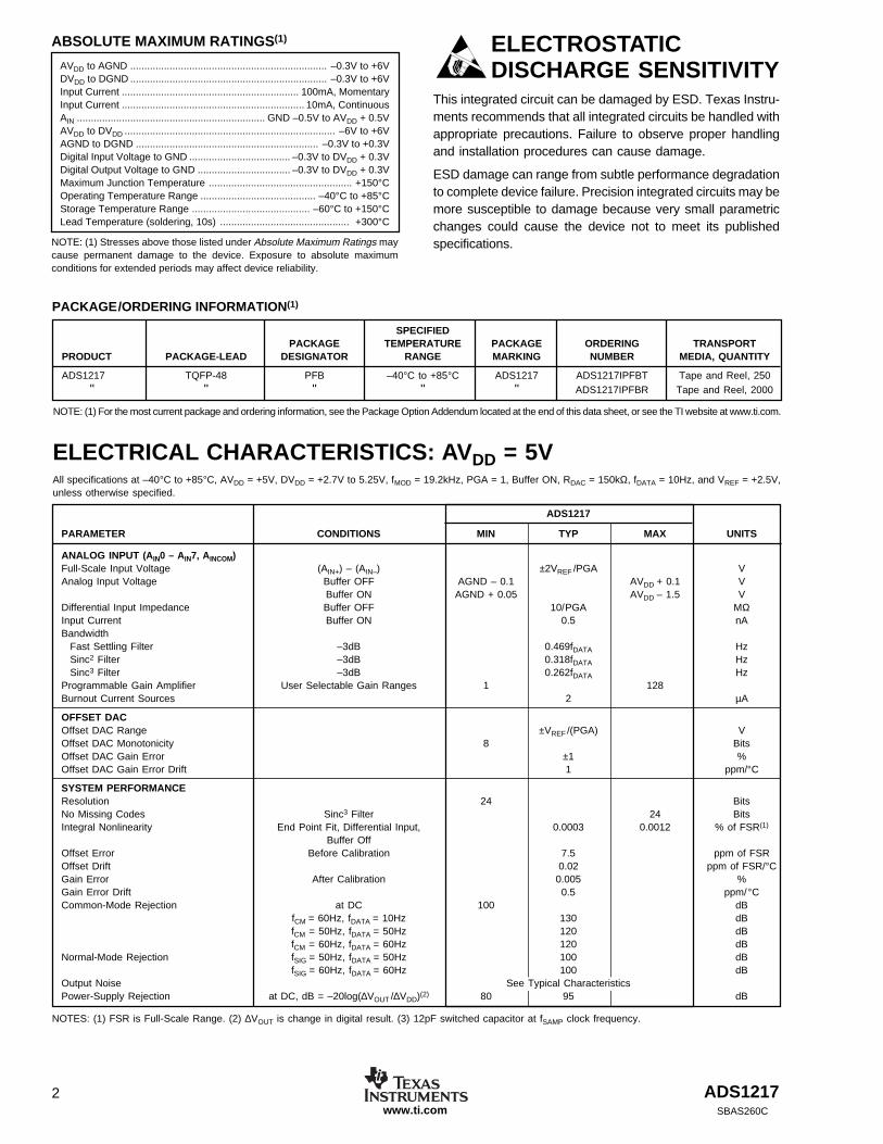
ABSOLUTE MAXIMUM RATINGS(1) ELECTROSTATICDISCHARGE SENSITIVITY
This integrated circuit can be damaged by ESD. Texas Instru-ments recommends that all integrated circuits be handled withappropriate precautions. Failure to observe proper handlingand installation procedures can cause damage.
ESD damage can range from subtle performance degradationto complete device failure. Precision integrated circuits may bemore susceptible to damage because very small parametricchanges could cause the device not to meet its publishedspecifications.
SPECIFIEDPACKAGE TEMPERATURE PACKAGE ORDERING TRANSPORT
PRODUCT PACKAGE-LEAD DESIGNATOR RANGE MARKING NUMBER MEDIA, QUANTITY
ADS1217 TQFP-48 PFB –40°C to +85°C ADS1217 ADS1217IPFBT Tape and Reel, 250" " " " " ADS1217IPFBR Tape and Reel, 2000
NOTE: (1) For the most current package and ordering information, see the Package Option Addendum located at the end of this data sheet, or see the TI website at www.ti.com.
PACKAGE/ORDERING INFORMATION(1)
ADS1217
PARAMETER CONDITIONS MIN TYP MAX UNITS
ANALOG INPUT (AIN0 – AIN7, AINCOM)Full-Scale Input Voltage (AIN+) – (AIN–) ±2VREF /PGA VAnalog Input Voltage Buffer OFF AGND – 0.1 AVDD + 0.1 V
Buffer ON AGND + 0.05 AVDD – 1.5 VDifferential Input Impedance Buffer OFF 10/PGA MΩInput Current Buffer ON 0.5 nABandwidth
Fast Settling Filter –3dB 0.469fDATA HzSinc2 Filter –3dB 0.318fDATA HzSinc3 Filter –3dB 0.262fDATA Hz
Programmable Gain Amplifier User Selectable Gain Ranges 1 128Burnout Current Sources 2 µA
OFFSET DACOffset DAC Range ±VREF /(PGA) VOffset DAC Monotonicity 8 BitsOffset DAC Gain Error ±1 %Offset DAC Gain Error Drift 1 ppm/°C
SYSTEM PERFORMANCEResolution 24 BitsNo Missing Codes Sinc3 Filter 24 BitsIntegral Nonlinearity End Point Fit, Differential Input, 0.0003 0.0012 % of FSR(1)
Buffer OffOffset Error Before Calibration 7.5 ppm of FSROffset Drift 0.02 ppm of FSR/°CGain Error After Calibration 0.005 %Gain Error Drift 0.5 ppm/°CCommon-Mode Rejection at DC 100 dB
fCM = 60Hz, fDATA = 10Hz 130 dBfCM = 50Hz, fDATA = 50Hz 120 dBfCM = 60Hz, fDATA = 60Hz 120 dB
Normal-Mode Rejection fSIG = 50Hz, fDATA = 50Hz 100 dBfSIG = 60Hz, fDATA = 60Hz 100 dB
Output Noise See Typical CharacteristicsPower-Supply Rejection at DC, dB = –20log(∆VOUT /∆VDD)(2) 80 95 dB
NOTES: (1) FSR is Full-Scale Range. (2) ∆VOUT is change in digital result. (3) 12pF switched capacitor at fSAMP clock frequency.

ADS1217SBAS260C
3www.ti.com
ELECTRICAL CHARACTERISTICS: AVDD = 5V (Cont.)All specifications at –40°C to +85°C, AVDD = +5V, DVDD = +2.7V to 5.25V, fMOD = 19.2kHz, PGA = 1, Buffer ON, RDAC = 150kΩ, fDATA = 10Hz, and VREF = +2.5V,unless otherwise specified.
ADS1217
PARAMETER CONDITIONS MIN TYP MAX UNITS
VOLTAGE REFERENCE INPUTReference Input (VREF) VREF ≡ (VREF+) – (VREF–) 0.1 2.5 2.6 VNegative Reference Input (VREF–) AGND – 0.1 (VREF+) – 0.1 VPositive Reference Input (VREF+) (VREF–) + 0.1 AVDD + 0.1 VCommon-Mode Rejection at DC 120 dBCommon-Mode Rejection fVREFCM = 60Hz, fDATA = 60Hz 120 dBBias Current(3) VREF = 2.5V, PGA = 1 1.3 µA
ON-CHIP VOLTAGE REFERENCEOutput Voltage REF HI = 1 2.4 2.5 2.6 V
REF HI = 0 1.25 VShort-Circuit Current Source 8 mAShort-Circuit Current Sink 50 µADrift 15 ppm/°CNoise VRCAP = 0.1µF, BW = 0.1Hz to 100Hz 10 µVrmsOutput Impedance Sourcing 100µA 3 ΩStartup Time 5 ms
IDACFull-Scale Output Current RDAC = 150kΩ, Range = 1 0.5 mA
RDAC = 150kΩ, Range = 2 1 mARDAC = 150kΩ, Range = 3 2 mARDAC = 15kΩ, Range = 3 20 mA
Current Setting Resistance (RDAC) 10 kΩMonotonicity RDAC = 150kΩ 8 BitsCompliance Voltage 0 AVDD – 1 VOutput Impedance See Typical CharacteristicsPSRR VOUT = AVDD/2, Code > 16 400 ppm/VGain Error Individual IDAC 5 %Gain Error Drift Individual IDAC 75 ppm/°CGain Error Mismatch Between IDACs, Same Range and Code 0.25 %Gain Error Mismatch Drift Between IDACs, Same Range and Code 15 ppm/°C
POWER-SUPPLY REQUIREMENTSPower-Supply Voltage AVDD 4.75 5.25 VAnalog Current (IADC + IVREF + IIDAC) PDWN = 0, or SLEEP 1 nA
A/D Converter Current (IADC) PGA = 1, Buffer OFF 175 275 µAPGA = 128, Buffer OFF 500 750 µA
PGA = 1, Buffer ON 250 350 µAPGA = 128, Buffer ON 900 1375 µA
VREF Current (IVREF) 250 375 µAIIDAC Current (IIDAC) Excludes Load Current 480 675 µA
Digital Current Normal Mode, DVDD = 5V 180 275 µASLEEP Mode, DVDD = 5V 150 µA
Read Data Continuous Mode, DVDD = 5V 230 µAPDWN = 0 1 nA
Power Dissipation PGA = 1, Buffer OFF, REFEN = 0, 1.8 2.8 mWIDACs OFF, DVDD = 5V
NOTES: (1) FSR is Full-Scale Range. (2) ∆VOUT is change in digital result. (3) 12pF switched capacitor at fSAMP clock frequency.

ADS12174SBAS260Cwww.ti.com
ELECTRICAL CHARACTERISTICS: AVDD = 3VAll specifications at –40°C to +85°C, AVDD = +3V, DVDD = +2.7V to 5.25V, fMOD = 19.2kHz, PGA = 1, Buffer ON, RDAC = 75kΩ, fDATA = 10Hz, and VREF = +1.25V,unless otherwise specified.
ADS1217
PARAMETER CONDITIONS MIN TYP MAX UNITS
ANALOG INPUT (AIN0 – AIN7, AINCOM)Full-Scale Input Voltage (AIN+) – (AIN–) ±2VREF /PGA VAnalog Input Range Buffer OFF AGND – 0.1 AVDD + 0.1 V
Buffer ON AGND + 0.05 AVDD – 1.5 VInput Impedance Buffer OFF 10/PGA MΩInput Current Buffer ON 0.5 nABandwidth
Fast Settling Filter –3dB 0.469fDATA HzSinc2 Filter –3dB 0.318fDATA HzSinc3 Filter –3dB 0.262fDATA Hz
Programmable Gain Amplifier User Selectable Gain Ranges 1 128Burnout Current Sources 2 µA
OFFSET DACOffset DAC Range ±VREF /(PGA) VOffset DAC Monotonicity 8 BitsOffset DAC Gain Error ±1 %Offset DAC Gain Error Drift 2 ppm/°C
SYSTEM PERFORMANCEResolution 24 BitsNo Missing Codes Sinc3 Filter 24 BitsIntegral Nonlinearity End Point Fit, Differential Input, 0.0003 0.0012 % of FSR(1)
Buffer Off, T = 25°COffset Error Before Calibration 15 ppm of FSROffset Drift 0.04 ppm of FSR/°CGain Error After Calibration 0.010 %Gain Error Drift 1.0 ppm/°CCommon-Mode Rejection at DC 100 dB
fCM = 60Hz, fDATA = 10Hz 130 dBfCM = 50Hz, fDATA = 50Hz 120 dBfCM = 60Hz, fDATA = 60Hz 120 dB
Normal-Mode Rejection fSIG = 50Hz, fDATA = 50Hz 100 dBfSIG = 60Hz, fDATA = 60Hz 100 dB
Output Noise See Typical CharacteristicsPower-Supply Rejection at DC, dB = –20 log(∆VOUT /∆VDD)(2) 75 90 dB
VOLTAGE REFERENCE INPUTReference Input (VREF) VREF ≡ (VREF+) – (VREF–) 0.1 1.25 1.3 VNegative Reference Input (VREF–) AGND – 0.1 (VREF+) – 0.1 VPositive Reference Input (VREF+) (VREF–) + 0.1 AVDD + 0.1 VCommon-Mode Rejection at DC 120 dBCommon-Mode Rejection fVREFCM = 60Hz, fDATA = 60Hz 120 dBBias Current(3) VREF = 1.25V 0.65 µA
ON-CHIP VOLTAGE REFERENCEOutput Voltage REF HI = 0 1.2 1.25 1.3 VShort-Circuit Current Source 3 mAShort-Circuit Current Sink 50 µADrift 15 ppm/°CNoise VRCAP = 0.1µF, BW = 0.1Hz to 100Hz 10 µVrmsOutput Impedance Sourcing 100µA 3 ΩStartup Time 5 ms
IDACFull-Scale Output Current RDAC = 75kΩ, Range = 1 0.5 mA
RDAC = 75kΩ, Range = 2 1 mARDAC = 75kΩ, Range = 3 2 mARDAC = 15kΩ, Range = 3 20 mA
Current Setting Resistance (RDAC) 10 kΩMonotonicity RDAC = 75kΩ 8 BitsCompliance Voltage 0 AVDD – 1 VOutput Impedance See Typical CharacteristicsPSRR VOUT = AVDD /2, Code > 16 600 ppm/VGain Error Individual IDAC 5 %Gain Error Drift Individual IDAC 75 ppm/°CGain Error Mismatch Between IDACs, Same Range and Code 0.25 %Gain Error Mismatch Drift Between IDACs, Same Range and Code 15 ppm/°C
NOTES: (1) FSR is Full-Scale Range. (2) ∆VOUT is change in digital result. (3) 12pF switched capacitor at fSAMP clock frequency.

ADS1217SBAS260C
5www.ti.com
POWER-SUPPLY REQUIREMENTSPower-Supply Voltage AVDD 2.7 3.3 VAnalog Current (IADC + IVREF + IIDAC) PDWN = 0, or SLEEP 1 nA
A/D Converter Current (IADC) PGA = 1, Buffer OFF 160 250 µAPGA = 128, Buffer OFF 450 700 µA
PGA = 1, Buffer ON 230 325 µAPGA = 128, Buffer ON 850 1325 µA
VREF Current (IVREF) 250 375 µAIIDAC Current (IIDAC) Excludes Load Current 480 675 µA
Digital Current Normal Mode, DVDD = 3V 90 200 µASLEEP Mode, DVDD = 3V 75 µA
Read Data Continuous Mode, DVDD = 3V 113 µAPDWN = 0 1 nA
Power Dissipation PGA = 1, Buffer OFF, REFEN = 0, 0.8 1.4 mWIDACs OFF, DVDD = 3V
NOTES: (1) FSR is Full-Scale Range. (2) ∆VOUT is change in digital result. (3) 12pF switched capacitor at fSAMP clock frequency.
ADS1217
PARAMETER CONDITIONS MIN TYP MAX UNITS
ELECTRICAL CHARACTERISTICS: AVDD = 3V (Cont.)All specifications at –40°C to +85°C, AVDD = +3V, DVDD = +2.7V to 5.25V, fMOD = 19.2kHz, PGA = 1, Buffer ON, RDAC = 75kΩ, fDATA = 10Hz, and VREF = +1.25V,unless otherwise specified.
PARAMETER CONDITIONS MIN TYP MAX UNITS
INPUT/OUTPUTLogic Level
VIH 0.8 × DVDD DVDD VVIL
(1) DGND 0.2 × DVDD VVOH IOH = 1mA DVDD – 0.4 VVOL IOL = 1mA DGND DGND + 0.4 V
Input Leakage: IIN 0 < VI < DVDD –10 10 µA
CLOCK RATESMaster Clock Rate: fOSC 1 8 MHzMaster Clock Period: tOSC 1/fOSC 125 1000 ns
NOTE: (1) Maximum VIL for XIN is DGND + 0.05V.
ELECTRICAL CHARACTERISTICS: DigitalAll specifications at –40°C to +85°C, and DVDD = +2.7V to 5.25V.
ADS12176SBAS260Cwww.ti.com
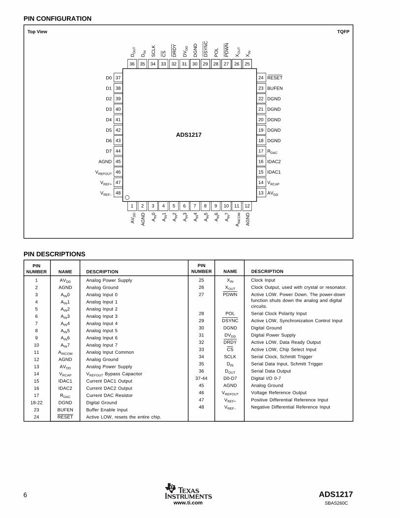
PIN CONFIGURATION
PINNUMBER NAME DESCRIPTION
1 AVDD Analog Power Supply
2 AGND Analog Ground
3 AIN0 Analog Input 0
4 AIN1 Analog Input 1
5 AIN2 Analog Input 2
6 AIN3 Analog Input 3
7 AIN4 Analog Input 4
8 AIN5 Analog Input 5
9 AIN6 Analog Input 6
10 AIN7 Analog Input 7
11 AINCOM Analog Input Common
12 AGND Analog Ground
13 AVDD Analog Power Supply
14 VRCAP VREFOUT Bypass Capacitor
15 IDAC1 Current DAC1 Output
16 IDAC2 Current DAC2 Output
17 RDAC Current DAC Resistor
18-22 DGND Digital Ground
23 BUFEN Buffer Enable Input
24 RESET Active LOW, resets the entire chip.
PIN DESCRIPTIONS
PINNUMBER NAME DESCRIPTION
24
23
22
21
20
19
18
17
16
15
14
13
RESET
BUFEN
DGND
DGND
DGND
DGND
DGND
RDAC
IDAC2
IDAC1
VRCAP
AVDD
DO
UT
DIN
SC
LK
CS
DR
DY
DV
DD
DG
ND
DS
YN
C
PO
L
PD
WN
XO
UT
XIN
AV
DD
AG
ND
AIN
0
AIN
1
AIN
2
AIN
3
AIN
4
AIN
5
AIN
6
AIN
7
AIN
CO
M
AG
ND
37
38
39
40
41
42
43
44
45
46
47
48
D0
D1
D2
D3
D4
D5
D6
D7
AGND
VREFOUT
VREF+
VREF–
36 35 34 33 32 31 30 29 28 27 26
1 2 3 4 5 6 7 8 9 10 11
25
12
ADS1217
Top View TQFP
25 XIN Clock Input
26 XOUT Clock Output, used with crystal or resonator.
27 PDWN Active LOW. Power Down. The power-downfunction shuts down the analog and digitalcircuits.
28 POL Serial Clock Polarity Input
29 DSYNC Active LOW, Synchronization Control Input
30 DGND Digital Ground
31 DVDD Digital Power Supply
32 DRDY Active LOW, Data Ready Output
33 CS Active LOW, Chip Select Input
34 SCLK Serial Clock, Schmitt Trigger
35 DIN Serial Data Input, Schmitt Trigger
36 DOUT Serial Data Output
37-44 D0-D7 Digital I/O 0-7
45 AGND Analog Ground
46 VREFOUT Voltage Reference Output
47 VREF+ Positive Differential Reference Input
48 VREF– Negative Differential Reference Input

ADS1217SBAS260C
7www.ti.com
SPEC DESCRIPTION MIN MAX UNITS
t1 SCLK Period 4 tOSC Periods3 DRDY Periods
t2 SCLK Pulse Width, HIGH and LOW 200 nst3 CS LOW to First SCLK Edge; Setup Time(1) 0 nst4 DIN Valid to SCLK Edge; Setup Time 50 nst5 Valid DIN to SCLK Edge; Hold Time 50 nst6 Delay Between Last SCLK Edge for DIN and First SCLK
Edge for DOUT:RDATA, RDATAC, RREG, WREG, RRAM, WRAM 50 tOSC PeriodsCSREG, CSRAMX, CSRAM 200 tOSC PeriodsCSARAM, CSARAMX 1100 tOSC Periods
t7(2) SCLK Edge to Valid New DOUT 50 nst8(2) SCLK Edge to DOUT, Hold Time 0 nst9 Last SCLK Edge to DOUT Tri-State 6 10 tOSC Periods
NOTE: DOUT goes tri-state immediately when CS goes HIGH.t10 CS LOW Time After Final SCLK Edge 0 nst11 Final SCLK Edge of One Op Code Until First Edge SCLK
of Next Command:RREG, WREG, RRAM, WRAM, CSRAMX, CSARAMX, tOSC Periods
CSRAM, CSARAM, CSREG, DSYNC, SLEEP, RDATA,RDATAC, STOPC 4 tOSC Periods
CREG, CRAM 220 tOSC PeriodsCREGA 1600 tOSC PeriodsSELFGCAL, SELFOCAL, SYSOCAL, SYSGCAL 7 DRDY PeriodsSELFCAL 14 DRDY PeriodsRESET (Input pin, command, or SCLK pattern) 16 tOSC Periods
t12 300 500 tOSC Periodst13 5 tOSC Periodst14 550 750 tOSC Periodst15 1050 1250 tOSC Periodst16 Pulse Width 4 tOSC Periodst17 Data Not Valid 4 tOSC Periods
NOTES: (1) CS may be tied LOW. (2) Load = 20pF.
TIMING DIAGRAMS
TIMING CHARACTERISTICS
t4
MSB
(Command or Command and Data)
LSB
t5
t1t3
CS
SCLK(POL = 0)
DIN
DOUT
NOTE: (1) Bit Order = 0.
SCLK Reset Waveform
t7
MSB(1) LSB(1)
t8
t10t2
t2 t11t6
t9
SCLK(POL = 1)
t12 t14 t15
t13 t13
SCLK
t17
DRDY
t16
RESET, DSYNC, PDWN
ADS1217Resets On
Falling Edge
ADS12178SBAS260Cwww.ti.com
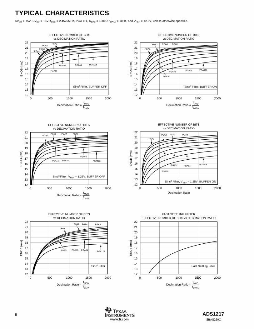
TYPICAL CHARACTERISTICSAVDD = +5V, DVDD = +5V, fOSC = 2.4576MHz, PGA = 1, RDAC = 150kΩ, fDATA = 10Hz, and VREF = +2.5V, unless otherwise specified.
22
21
20
19
18
17
16
15
14
13
12
EFFECTIVE NUMBER OF BITSvs DECIMATION RATIO
0 500 1000 1500 2000
EN
OB
(rm
s)
PGA4 PGA8PGA1 PGA2
PGA16 PGA32
PGA64
PGA128
Decimation Ratio =fMOD
fDATA
Sinc3 Filter, VREF = 1.25V, BUFFER OFF
22
21
20
19
18
17
16
15
14
13
12
EFFECTIVE NUMBER OF BITSvs DECIMATION RATIO
0 500 1000 1500 2000
EN
OB
(rm
s)
PGA4 PGA8
PGA1
PGA2
PGA32 PGA128PGA16 PGA64
Decimation Ratio =fMOD
fDATA
Sinc2 Filter
22
21
20
19
18
17
16
15
14
13
12
FAST SETTLING FILTEREFFECTIVE NUMBER OF BITS vs DECIMATION RATIO
0 500 1000 1500 2000
EN
OB
(rm
s)
1500
Decimation Ratio =fMOD
fDATA
Fast Settling Filter
22
21
20
19
18
17
16
15
14
13
12
EFFECTIVE NUMBER OF BITSvs DECIMATION RATIO
Decimation Ratio =fMOD
fDATA
0 500 1000 1500 2000
PGA4
EN
OB
(rm
s)
PGA2
PGA16
PGA1PGA8
PGA32 PGA64 PGA128
Sinc3 Filter, BUFFER OFF
22
21
20
19
18
17
16
15
14
13
12
EFFECTIVE NUMBER OF BITSvs DECIMATION RATIO
0 500 1000 1500 2000
EN
OB
(rm
s)
PGA4 PGA8
PGA1
PGA2
PGA16
PGA32PGA64 PGA128
Decimation Ratio =fMOD
fDATA
Sinc3 Filter, BUFFER ON
22
21
20
19
18
17
16
15
14
13
12
EFFECTIVE NUMBER OF BITSvs DECIMATION RATIO
Decimation Ratio
0 500 1000 1500 2000
EN
OB
(rm
s)PGA4 PGA8
PGA1
PGA2
PGA16
PGA32 PGA64PGA128
Sinc3 Filter, VREF = 1.25V, BUFFER ON
ADS1217SBAS260C
9www.ti.com
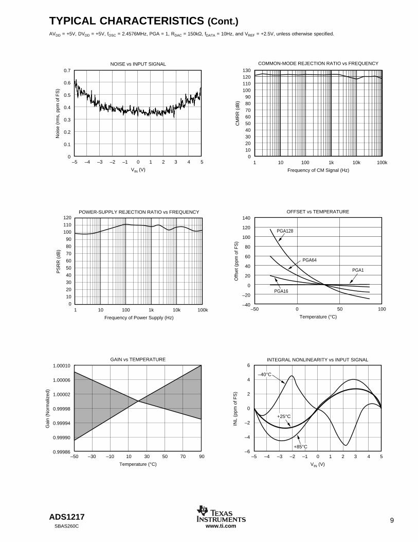
TYPICAL CHARACTERISTICS (Cont.)AVDD = +5V, DVDD = +5V, fOSC = 2.4576MHz, PGA = 1, RDAC = 150kΩ, fDATA = 10Hz, and VREF = +2.5V, unless otherwise specified.
0.7
0.6
0.5
0.4
0.3
0.2
0.1
0
NOISE vs INPUT SIGNAL
VIN (V)
–5 –3–4 10 2–1–2 3 4 5
Noi
se (
rms,
ppm
of F
S)
1301201101009080706050403020100
COMMON-MODE REJECTION RATIO vs FREQUENCY
Frequency of CM Signal (Hz)
1 10 100 1k 10k 100k
CM
RR
(dB
)
120
110
100
90
80
70
60
50
40
30
20
10
0
POWER-SUPPLY REJECTION RATIO vs FREQUENCY
Frequency of Power Supply (Hz)
1 10 1k100 10k 100k
PS
RR
(dB
)
1.00010
1.00006
1.00002
0.99998
0.99994
0.99990
0.99986
GAIN vs TEMPERATURE
Temperature (°C)
–50 –30 10–10 30 50 70 90
Gai
n (N
orm
aliz
ed)
140
120
100
80
60
40
20
0
–20
–40
OFFSET vs TEMPERATURE
Offs
et (
ppm
of F
S)
Temperature (°C)
–50 0 50 100
PGA128
PGA16
PGA64
PGA1
6
4
2
0
–2
–4
–6
INTEGRAL NONLINEARITY vs INPUT SIGNAL
VIN (V)
–5 –4 –2 –1–3 0 1 2 3 4 5
INL
(ppm
of F
S)
+25°C
–40°C
+85°C

ADS121710SBAS260Cwww.ti.com
TYPICAL CHARACTERISTICS (Cont.)AVDD = +5V, DVDD = +5V, fOSC = 2.4576MHz, PGA = 1, RDAC = 150kΩ, fDATA = 10Hz, and VREF = +2.5V, unless otherwise specified.
2.55
2.50
2.45
VREFOUT vs LOAD CURRENT
VREFOUT Current Load (mA)
–0.5 0 0.5 1.0 1.5 2.0 2.5
VR
EF
OU
T (
V)
200
170
140
110
80
50
20
–10
–40
–70
–100
OFFSET DAC: OFFSET vs TEMPERATURE
Offs
et (
ppm
of F
SR
)
Temperature (°C)
–50 –30 10–10 30 50 70 90
270
240
210
180
150
CURRENT vs TEMPERATURE
Cur
rent
(µA
)
IANALOG
IDIGITAL
Temperature (°C)
–60 –30 0 30 60 90 120
400
350
300
250
200
150
100
50
0
DIGITAL CURRENT
VDD (V)
2.5 3.0 3.5 4.0 4.5 5 5.5
Cur
rent
(µA
)
Normal4.91MHz
SLEEP4.91MHz
SLEEP2.45MHz
Normal2.45MHz
5000
4000
3000
2000
1000
0
HISTOGRAM OF OUTPUT DATA
ppm of FS
–2.0
Num
ber
of O
ccur
renc
es
–1.5 –1.0 –0.5 0 0.5 1.0 1.5 2.0
900
800
700
600
500
400
300
200
100
0
A/D CURRENT vs PGA
PGA Setting
1 82 4 3216 12864
I AD
C (
µA)
AVDD = 5V, Buffer = ON
AVDD = 3V, Buffer = ON
Buffer = OFF
Buffer = OFF

ADS1217SBAS260C
11www.ti.com
TYPICAL CHARACTERISTICS (Cont.)AVDD = +5V, DVDD = +5V, fOSC = 2.4576MHz, PGA = 1, RDAC = 150kΩ, fDATA = 10Hz, and VREF = +2.5V, unless otherwise specified.
1.00020
1.00016
1.00012
1.00008
1.00004
1.00000
0.99996
0.99992
0.99988
0.99984
0.99980
0.99976
OFFSET DAC: GAIN vs TEMPERATURE
Nor
mal
ized
Gai
n
Temperature (°C)
–50 –30 10–10 30 50 70 90
1.0000
1.000
0.999
0.999
0.998
IDAC IOUT vs VOUT
VDD – VOUT (V)
0 1 2 3 4 5
I OU
T (
Nor
mal
ized
)
+85°C
–40°C
+25°C
1.010
1.005
1.000
0.995
0.990
0.985
IDAC NORMALIZED IOUT vs TEMPERATURE
I OU
T (
Nor
mal
ized
)
Temperature (°C)
–50 –30 10–10 30 50 70 90
3000
2000
1000
0
–1000
–2000
–3000
–4000
–5000
–6000
IDAC MATCHING vs TEMPERATURE
IDA
C M
atch
(pp
m)
Temperature (°C)
–50 –30 10–10 30 50 70 90
0.5
0.4
0.3
0.2
0.1
0
–0.1
–0.2
–0.3
–0.4
–0.5
IDAC DIFFERENTIAL NONLINEARITY(Range = 1, RDAC = 150kΩ, VREF = 2.5V)
IDAC Code
0 25532 64 96 128 160 192 224
DN
L (L
SB
)
0.5
0.4
0.3
0.2
0.1
0
–0.1
–0.2
–0.3
–0.4
–0.5
IDAC INTEGRAL NONLINEARITY(Range = 1, RDAC = 150kΩ, VREF = 2.5V)
IDAC Code
0 25532 64 96 128 160 192 224
INL
(LS
B)
ADS121712SBAS260Cwww.ti.com
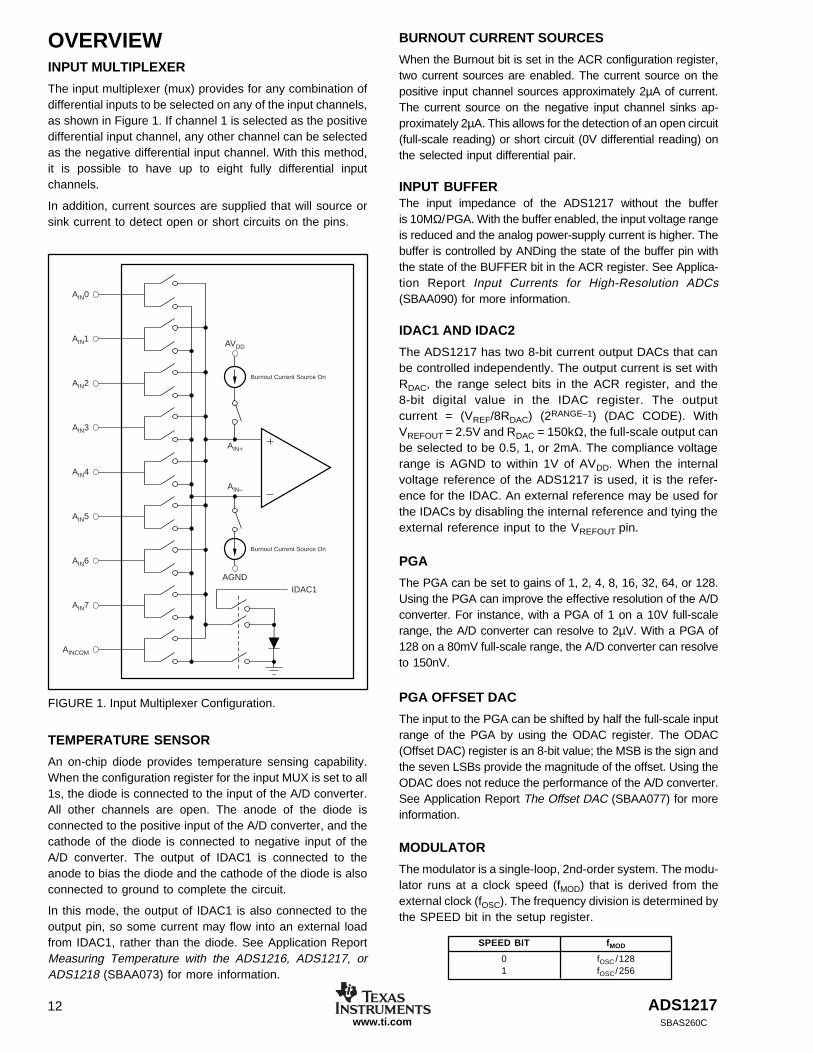
OVERVIEWINPUT MULTIPLEXER
The input multiplexer (mux) provides for any combination ofdifferential inputs to be selected on any of the input channels,as shown in Figure 1. If channel 1 is selected as the positivedifferential input channel, any other channel can be selectedas the negative differential input channel. With this method,it is possible to have up to eight fully differential inputchannels.
In addition, current sources are supplied that will source orsink current to detect open or short circuits on the pins.
BURNOUT CURRENT SOURCES
When the Burnout bit is set in the ACR configuration register,two current sources are enabled. The current source on thepositive input channel sources approximately 2µA of current.The current source on the negative input channel sinks ap-proximately 2µA. This allows for the detection of an open circuit(full-scale reading) or short circuit (0V differential reading) onthe selected input differential pair.
INPUT BUFFERThe input impedance of the ADS1217 without the bufferis 10MΩ/PGA. With the buffer enabled, the input voltage rangeis reduced and the analog power-supply current is higher. Thebuffer is controlled by ANDing the state of the buffer pin withthe state of the BUFFER bit in the ACR register. See Applica-tion Report Input Currents for High-Resolution ADCs(SBAA090) for more information.
IDAC1 AND IDAC2
The ADS1217 has two 8-bit current output DACs that canbe controlled independently. The output current is set withRDAC, the range select bits in the ACR register, and the8-bit digital value in the IDAC register. The outputcurrent = (VREF/8RDAC) (2RANGE–1) (DAC CODE). WithVREFOUT = 2.5V and RDAC = 150kΩ, the full-scale output canbe selected to be 0.5, 1, or 2mA. The compliance voltagerange is AGND to within 1V of AVDD. When the internalvoltage reference of the ADS1217 is used, it is the refer-ence for the IDAC. An external reference may be used forthe IDACs by disabling the internal reference and tying theexternal reference input to the VREFOUT pin.
PGA
The PGA can be set to gains of 1, 2, 4, 8, 16, 32, 64, or 128.Using the PGA can improve the effective resolution of the A/Dconverter. For instance, with a PGA of 1 on a 10V full-scalerange, the A/D converter can resolve to 2µV. With a PGA of128 on a 80mV full-scale range, the A/D converter can resolveto 150nV.
PGA OFFSET DAC
The input to the PGA can be shifted by half the full-scale inputrange of the PGA by using the ODAC register. The ODAC(Offset DAC) register is an 8-bit value; the MSB is the sign andthe seven LSBs provide the magnitude of the offset. Using theODAC does not reduce the performance of the A/D converter.See Application Report The Offset DAC (SBAA077) for moreinformation.
MODULATOR
The modulator is a single-loop, 2nd-order system. The modu-lator runs at a clock speed (fMOD) that is derived from theexternal clock (fOSC). The frequency division is determined bythe SPEED bit in the setup register.
AIN3
AIN4
AIN+
AIN–
AIN5
AIN6
AIN0
AIN1
AIN2
AIN7
AINCOM
Burnout Current Source On
Burnout Current Source On
IDAC1AGND
AVDD
FIGURE 1. Input Multiplexer Configuration.
TEMPERATURE SENSOR
An on-chip diode provides temperature sensing capability.When the configuration register for the input MUX is set to all1s, the diode is connected to the input of the A/D converter.All other channels are open. The anode of the diode isconnected to the positive input of the A/D converter, and thecathode of the diode is connected to negative input of theA/D converter. The output of IDAC1 is connected to theanode to bias the diode and the cathode of the diode is alsoconnected to ground to complete the circuit.
In this mode, the output of IDAC1 is also connected to theoutput pin, so some current may flow into an external loadfrom IDAC1, rather than the diode. See Application ReportMeasuring Temperature with the ADS1216, ADS1217, orADS1218 (SBAA073) for more information.
SPEED BIT fMOD
0 fOSC /1281 fOSC/256

ADS1217SBAS260C
13www.ti.com
VOLTAGE REFERENCE INPUT
The ADS1217 uses a differential voltage reference input.The input signal is measured against the differential voltageVREF ≡ (VREF+) – (VREF–). For AVDD = 5V, VREF is typically2.5V. For AVDD = 3V, VREF is typically 1.25V. Due to thesampling nature of the modulator, the reference input currentincreases with higher modulator clock frequency (fMOD) andhigher PGA settings.
ON-CHIP VOLTAGE REFERENCE
A selectable voltage reference (1.25V or 2.5V) is available forsupplying the voltage reference input. To use, connect VREF–
to AGND and VREF+ to VREFOUT. The enabling and voltageselection are controlled through bits REF EN and REF HI inthe setup register. The 2.5V reference requires AVDD = 5V.When using the on-chip voltage reference, the VREFOUT pinshould be bypassed with a 0.1µF capacitor to AGND.
VRCAP PIN
This pin provides a bypass cap for noise filtering on internalVREF circuitry only. As this is a sensitive pin, place thecapacitor as close as possible and avoid any resistive load-ing. The recommended capacitor is a 0.001µF ceramic cap.If an external VREF is used, this pin can be left unconnected.
CLOCK GENERATOR
The clock source for the ADS1217 can be provided from acrystal, oscillator, or external clock. When the clock source isa crystal, external capacitors must be provided to ensure start-up and a stable clock frequency; see Figure 2 and Table I.
FIGURE 3. Filter Step Responses.
SETTLING TIMEFILTER (Conversion Cycles)
Sinc3 3Sinc2 2Fast 1
CONVERSION CYCLE
1 2 3 4+
Fast Sinc2 Sinc3 Sinc3
AUTO MODE FILTER SELECTION
FILTER SETTLING TIME
Adjustable Digital Filter
Data OutModulator
Output
Fast Settling
Sinc2
Sinc3
complete both an offset and gain calibration. Self-gain cali-bration is optimized for PGA gains less than 8. When usinghigher gains, system gain calibration is recommended.
For system calibration, the appropriate signal must beapplied to the inputs. The system offset command requires a“zero” differential input signal. It then computes an offset thatwill nullify offset in the system. The system gain commandrequires a positive “full-scale” differential input signal. It thencomputes a value to nullify gain errors in the system. Each ofthese calibrations will take seven tDATA periods to complete.
Calibration must be performed after power on, a change indecimation ratio, or a change of the PGA. For operation witha reference voltage greater than (AVDD – 1.5V), the buffermust also be turned off during calibration.
At the completion of calibration, the DRDY signal goes LOW,which indicates the calibration is finished and valid data isavailable. See Application Report Calibration Routine andRegister Value Generation for the ADS121x Series (SBAA099)for more information.
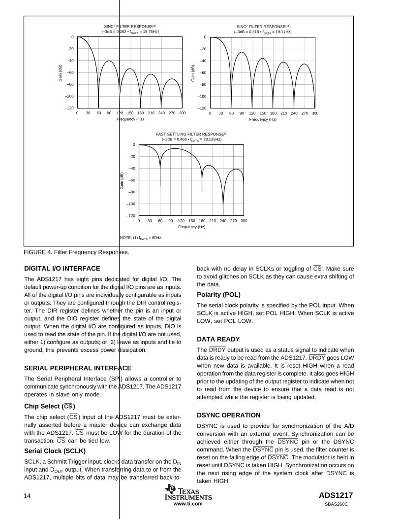
DIGITAL FILTER
The Digital Filter can use either the fast settling, sinc2, orsinc3 filter, as shown in Figure 3. In addition, the Auto modechanges the sinc filter after the input channel or PGA ischanged. When switching to a new channel, it will use thefast settling filter; It will then use the sinc2 followed by thesinc3 filter. This combines the low-noise advantage of thesinc3 filter with the quick response of the fast settling timefilter. See Figure 4 for the frequency response of each filter.
When using the fast setting filter, select a decimation valueset by the DEC0 and M/DEC1 registers that is evenlydivisible by four for the best gain accuracy. For example,choose 260 rather than 261.
FIGURE 2. Crystal Connection.
CLOCK PARTSOURCE FREQUENCY C1 C2 NUMBER
Crystal 2.4576 0-20pF 0-20pF ECS, ECSD 2.45 - 32
Crystal 4.9152 0-20pF 0-20pF ECS, ECSL 4.91
Crystal 4.9152 0-20pF 0-20pF ECS, ECSD 4.91
Crystal 4.9152 0-20pF 0-20pF CTS, MP 042 4M9182
TABLE I. Typical Clock Sources.
C1
Crystal
XIN
XOUTC2
CALIBRATION
The offset and gain errors in the ADS1217, or the completesystem, can be reduced with calibration. Internal calibrationof the ADS1217 is called self calibration. This is handled withthree commands. One command does both offset and gaincalibration. There is also a gain calibration command and anoffset calibration command. Each calibration process takesseven tDATA periods to complete. It takes 14 tDATA periods to
ADS121714SBAS260Cwww.ti.com
DIGITAL I/O INTERFACE
The ADS1217 has eight pins dedicated for digital I/O. Thedefault power-up condition for the digital I/O pins are as inputs.All of the digital I/O pins are individually configurable as inputsor outputs. They are configured through the DIR control regis-ter. The DIR register defines whether the pin is an input oroutput, and the DIO register defines the state of the digitaloutput. When the digital I/O are configured as inputs, DIO isused to read the state of the pin. If the digital I/O are not used,either 1) configure as outputs; or, 2) leave as inputs and tie toground, this prevents excess power dissipation.
SERIAL PERIPHERAL INTERFACE
The Serial Peripheral Interface (SPI) allows a controller tocommunicate synchronously with the ADS1217. The ADS1217operates in slave only mode.
Chip Select (CS)
The chip select (CS) input of the ADS1217 must be exter-nally asserted before a master device can exchange datawith the ADS1217. CS must be LOW for the duration of thetransaction. CS can be tied low.
Serial Clock (SCLK)
SCLK, a Schmitt Trigger input, clocks data transfer on the DIN
input and DOUT output. When transferring data to or from theADS1217, multiple bits of data may be transferred back-to-
back with no delay in SCLKs or toggling of CS . Make sureto avoid glitches on SCLK as they can cause extra shifting ofthe data.
Polarity (POL)
The serial clock polarity is specified by the POL input. WhenSCLK is active HIGH, set POL HIGH. When SCLK is activeLOW, set POL LOW.
DATA READY
The DRDY output is used as a status signal to indicate whendata is ready to be read from the ADS1217. DRDY goes LOWwhen new data is available. It is reset HIGH when a readoperation from the data register is complete. It also goes HIGHprior to the updating of the output register to indicate when notto read from the device to ensure that a data read is notattempted while the register is being updated.
DSYNC OPERATION
DSYNC is used to provide for synchronization of the A/Dconversion with an external event. Synchronization can beachieved either through the DSYNC pin or the DSYNCcommand. When the DSYNC pin is used, the filter counter isreset on the falling edge of DSYNC. The modulator is held inreset until DSYNC is taken HIGH. Synchronization occurs onthe next rising edge of the system clock after DSYNC istaken HIGH.
FIGURE 4. Filter Frequency Responses.
SINC3 FILTER RESPONSE(1)
(–3dB = 0.262 • fDATA = 15.76Hz)
Frequency (Hz)
0
–20
–40
–60
–80
–100
–1200 30 12060 90 150 180 210 240 270 300
Gai
n (d
B)
SINC2 FILTER RESPONSE(1)
(–3dB = 0.318 • fDATA = 19.11Hz)
Frequency (Hz)
0
–20
–40
–60
–80
–100
–1200 30 12060 90 150 180 210 240 270 300
Gai
n (d
B)
FAST SETTLING FILTER RESPONSE(1)
(–3dB = 0.469 • fDATA = 28.125Hz)
Frequency (Hz)
0
–20
–40
–60
–80
–100
–1200
NOTE: (1) fDATA = 60Hz.
30 12060 90 150 180 210 240 270 300
Gai
n (d
B)

ADS1217SBAS260C
15www.ti.com
When the DSYNC command is sent, the filter counter is reseton the edge of the last SCLK on the DSYNC command. Themodulator is held in reset until the next edge of SCLK isdetected. Synchronization occurs on the next rising edge ofthe system clock after the first SCLK after the DSYNCcommand. After a DSYNC operation, DRDY is held HIGHuntil valid data is ready.
RESET
There are three methods to reset the ADS1217: the RESETinput, the RESET command, and a special SCLK input pat-tern. When using the RESET input, take it LOW to force areset. Make sure to follow the minimum pulse width timingspecifications before taking the RESET input back high. Also,avoid glitches on the RESET input as these may causeaccidental resets. The RESET command takes effect after all8 bits have been shifted into DIN. Afterwards, the resetreleases automatically. The ADS1217 can also be reset witha special pattern on SCLK, see the Timing Diagram. Resetoccurs on the falling edge of the last SCLK edge in the pattern(for POL = 0). Afterwards, the reset releases automatically.
POWER-UP—SUPPLY VOLTAGE RAMP RATE
The power-on reset circuitry was designed to accommodatedigital supply ramp rates as slow as 1V/10ms. To ensureproper operation, the power supply should ramp monotonically.
MEMORY
Two types of memory are used on the ADS1217: registersand RAM. 16 registers directly control the various functions(PGA, DAC value, Decimation Ratio, etc.) and can be directlyread or written. Collectively, the registers contain all theinformation needed to configure the part, such as dataformat, mux settings, calibration settings, decimation ratio,etc. Additional registers, such as output data, are accessedthrough dedicated instructions.
REGISTER BANK TOPOLOGY
The operation of the device is set up through individualregisters. The set of the 16 registers required to configure thedevice is referred to as a Register Bank, as shown in Figure 5.
Reads and Writes to Registers and RAM occur on a bytebasis. However, copies between registers and RAM occurson a bank basis. The RAM is independent of the Registers;that is, the RAM can be used as general-purpose RAM.
The ADS1217 supports any combination of eight analoginputs. With this flexibility, the device could easily supporteight unique configurations—one per input channel. In orderto facilitate this type of usage, eight separate register banksare available. Therefore, each configuration could be writtenonce and recalled as needed without having to seriallyretransmit all the configuration data. Checksum commandsare also included, which can be used to verify the integrity ofRAM.
ConfigurationRegisters16 bytes
SETUPMUXACR
IDAC1IDAC2ODAC
DIODIR
DEC0M/DEC1OCR0OCR1OCR2FSR0FSR1FSR2
RAM128 Bytes
Bank 216 bytes
Bank 716 bytes
Bank 016 bytes
The RAM provides eight “banks”, with a bank consisting of16 bytes. The total size of the RAM is 128 bytes. Copiesbetween the registers and RAM are performed on a bankbasis. Also, the RAM can be directly read or written throughthe serial interface on power-up. The banks allow separatestorage of settings for each input.
The RAM address space is linear, therefore accessing RAMis done using an auto-incrementing pointer. Access to RAMin the entire memory map can be done consecutively with-out having to address each bank individually. For example,if you were currently accessing bank 0 at offset 0FH (the lastlocation of bank 0), the next access would be bank 1 andoffset 00H. Any access after bank 7 and offset 0FH will wraparound to bank 0 and Offset 00H.
Although the Register Bank memory is linear, the concept ofaddressing the device can also be thought of in terms ofbank and offset addressing. Looking at linear and bankaddressing syntax, we have the following comparison: in thelinear memory map, the address 14H is equivalent to bank1 and offset 04H. Simply stated, the most significant four bitsrepresent the bank, and the least significant four bits repre-sent the offset. The offset is equivalent to the registeraddress for that bank of memory.
FIGURE 5. Memory Organization.

ADS121716SBAS260Cwww.ti.com
DETAILED REGISTER DEFINITIONSSETUP (Address 00H) Setup RegisterReset Value = iii01110
bit 7-5 Factory Programmed Bits
bit 4 SPEED: Modulator Clock Speed0 : fMOD = fOSC/128 (default)1 : fMOD = fOSC/256
bit 3 REF EN: Internal Voltage Reference Enable0 = Internal Voltage Reference Disabled1 = Internal Voltage Reference Enabled (default)
bit 2 REF HI: Internal Reference Voltage Select0 = Internal Reference Voltage = 1.25V1 = Internal Reference Voltage = 2.5V (default)
bit 1 BUF EN: Buffer Enable0 = Buffer Disabled1 = Buffer Enabled (default)
bit 0 BIT ORDER: Set Order Bits are Transmitted0 = Most Significant Bit Transmitted First (default)1 = Least Significant Bit Transmitted FirstData is always shifted into the part most significantbit first. Data is always shifted out of the part mostsignificant byte first. This configuration bit only con-trols the bit order within the byte of data that isshifted out.
ADDRESS REGISTER BIT 7 BIT 6 BIT 5 BIT 4 BIT 3 BIT 2 BIT 1 BIT 0
00H SETUP ID ID ID SPEED REF EN REF HI BUF EN BIT ORDER
01H MUX PSEL3 PSEL2 PSEL1 PSEL0 NSEL3 NSEL2 NSEL1 NSEL0
02H ACR BOCS IDAC2R1 IDAC2R0 IDAC1R1 IDAC1R0 PGA2 PGA1 PGA0
03H IDAC1 IDAC1_7 IDAC1_6 IDAC1_5 IDAC1_4 IDAC1_3 IDAC1_2 IDAC1_1 IDAC1_0
04H IDAC2 IDAC2_7 IDAC2_6 IDAC2_5 IDAC2_4 IDAC2_3 IDAC2_2 IDAC2_1 IDAC2_0
05H ODAC SIGN OSET_6 OSET_5 OSET_4 OSET_3 OSET_2 OSET_1 OSET_0
06H DIO DIO_7 DIO_6 DIO_5 DIO_4 DIO_3 DIO_2 DIO_1 DIO_0
07H DIR DIR_7 DIR_6 DIR_5 DIR_4 DIR_3 DIR_2 DIR_1 DIR_0
08H DEC0 DEC07 DEC06 DEC05 DEC04 DEC03 DEC02 DEC01 DEC00
09H M/DEC1 DRDY U/B SMODE1 SMODE0 Reserved DEC10 DEC09 DEC08
0AH OCR0 OCR07 OCR06 OCR05 OCR04 OCR03 OCR02 OCR01 OCR00
0BH OCR1 OCR15 OCR14 OCR13 OCR12 OCR11 OCR10 OCR09 OCR08
0CH OCR2 OCR23 OCR22 OCR21 OCR20 OCR19 OCR18 OCR17 OCR16
0DH FSR0 FSR07 FSR06 FSR05 FSR04 FSR03 FSR02 FSR01 FSR00
0EH FSR1 FSR15 FSR14 FSR13 FSR12 FSR11 FSR10 FSR09 FSR08
0FH FSR2 FSR23 FSR22 FSR21 FSR20 FSR19 FSR18 FSR17 FSR16
TABLE II. Registers.
REGISTER MAP
bit 7 bit 6 bit 5 bit 4 bit 3 bit 2 bit 1 bit 0
ID ID ID SPEED REF EN REF HI BUF EN BIT ORDER
bit 7 bit 6 bit 5 bit 4 bit 3 bit 2 bit 1 bit 0
PSEL3 PSEL2 PSEL1 PSEL0 NSEL3 NSEL2 NSEL1 NSEL0
MUX (Address 01H) Multiplexer Control RegisterReset Value = 01H
bit 7-4 PSEL3: PSEL2: PSEL1: PSEL0: Positive ChannelSelect0000 = AIN0 (default)0001 = AIN10010 = AIN20011 = AIN30100 = AIN40101 = AIN50110 = AIN60111 = AIN71xxx = AINCOM (except when all bits are 1s)1111 = Temperature Sensor Diode
bit 3-0 NSEL3: NSEL2: NSEL1: NSEL0: Negative ChannelSelect0000 = AIN00001 = AIN1 (default)0010 = AIN20011 = AIN30100 = AIN40101 = AIN50110 = AIN60111 = AIN71xxx = AINCOM (except when all bits are 1s)1111 = Temperature Sensor Diode

ADS1217SBAS260C
17www.ti.com
ACR (Address 02H) Analog Control RegisterReset Value = 00H
bit 7 BOCS: Burnout Current Source0 = Disabled (default)1 = Enabled
IDAC Current = VR
DAC CodeREF
DAC
RANGE
82 1
( )( )−
bit 6-5 IDAC2R1: IDAC2R0: Full-Scale Range Select forIDAC200 = Off (default)01 = Range 110 = Range 211 = Range 3
bit 4-3 IDAC1R1: IDAC1R0: Full-Scale Range Select forIDAC100 = Off (default)01 = Range 110 = Range 211 = Range 3
bit 2-0 PGA2: PGA1: PGA0: Programmable Gain AmplifierGain Selection000 = 1 (default)001 = 2010 = 4011 = 8100 = 16101 = 32110 = 64111 = 128
IDAC1 (Address 03H) Current DAC 1Reset Value = 00H
The DAC code bits set the output of DAC1 from 0 to full-scale. The value of the full-scale current is set by this Byte,VREF, RDAC, and the DAC1 range bits in the ACR register.
IDAC2 (Address 04H) Current DAC 2Reset Value = 00H
The DAC code bits set the output of DAC2 from 0 to full-scale. The value of the full-scale current is set by this Byte,VREF, RDAC, and the DAC2 range bits in the ACR register.
bit 7 bit 6 bit 5 bit 4 bit 3 bit 2 bit 1 bit 0
BOCS IDAC2R1 IDAC2R0 IDAC1R1 IDAC1R0 PGA2 PGA1 PGA0
bit 7 bit 6 bit 5 bit 4 bit 3 bit 2 bit 1 bit 0
IDAC1_7 IDAC1_6 IDAC1_5 IDAC1_4 IDAC1_3 IDAC1_2 IDAC1_1 IDAC1_0
bit 7 bit 6 bit 5 bit 4 bit 3 bit 2 bit 1 bit 0
IDAC2_7 IDAC2_6 IDAC2_5 IDAC2_4 IDAC1_3 IDAC1_2 IDAC1_1 IDAC1_0
ODAC (Address 05H) Offset DAC SettingReset Value = 00H
bit 7 Offset Sign0 = Positive
1 = Negative
bit 6-0 Offset = VPGA
CodeREF •
127
NOTE: The offset must be used after calibration or thecalibration will notify the effects.
DIO (Address 06H) Digital I/OReset Value = 00H
A value written to this register will appear on the digitalI/O pins if the pin is configured as an output in the DIRregister. Reading this register will return the value of thedigital I/O pins.
DIR (Address 07H) Direction control for digital I/OReset Value = FFH
Each bit controls whether the Digital I/O pin is an output(= 0) or input (= 1). The default power-up state is as inputs.
DEC0 (Address 08H) Decimation Register(Least Significant 8 bits)
Reset Value = 80H
The decimation value is defined with 11 bits for a range of 20to 2047. This register is the least significant 8 bits. The 3most significant bits are contained in the M/DEC1 register.The default data rate is 10Hz with a 2.4576MHz crystal.
bit 7 bit 6 bit 5 bit 4 bit 3 bit 2 bit 1 bit 0
SIGN OSET6 OSET5 OSET4 OSET3 OSET2 OSET1 OSET0
bit 7 bit 6 bit 5 bit 4 bit 3 bit 2 bit 1 bit 0
DIR7 DIR6 DIR5 DIR4 DIR3 DIR2 DIR1 DIR0
bit 7 bit 6 bit 5 bit 4 bit 3 bit 2 bit 1 bit 0
DEC07 DEC06 DEC05 DEC04 DEC03 DEC02 DEC01 DEC00
bit 7 bit 6 bit 5 bit 4 bit 3 bit 2 bit 1 bit 0
DIO7 DIO6 DIO5 DIO4 DIO3 DIO2 DIO1 DIO0

ADS121718SBAS260Cwww.ti.com
M/DEC1 (Address 09H) Mode and Decimation RegisterReset Value = 07H
bit 7 DRDY: Data Ready (Read Only)This bit duplicates the state of the DRDY pin.
bit 6 U/B: Data Format0 = Bipolar (default)1 = Unipolar
bit 5-4 SMODE1: SMODE0: Settling Mode00 = Auto (default)01 = Fast Settling filter10 = Sinc2 filter11 = Sinc3 filter
bit 2-0 DEC10: DEC09: DEC08: Most Significant Bits ofthe Decimation Value
OCR0 (Address 0AH) Offset Calibration Coefficient(Least Significant Byte)Reset Value = 00H
OCR1 (Address 0BH) Offset Calibration Coefficient(Middle Byte)Reset Value = 00H
U/B ANALOG INPUT DIGITAL OUTPUT
+FS 0x7FFFFF0 Zero 0x000000
–FS 0x800000+FS 0xFFFFFF
1 Zero 0x000000–FS 0x000000
bit 7 bit 6 bit 5 bit 4 bit 3 bit 2 bit 1 bit 0
OCR07 OCR06 OCR05 OCR04 OCR03 OCR02 OCR01 OCR00
bit 7 bit 6 bit 5 bit 4 bit 3 bit 2 bit 1 bit 0
OCR15 OCR14 OCR13 OCR12 OCR11 OCR10 OCR09 OCR08
bit 7 bit 6 bit 5 bit 4 bit 3 bit 2 bit 1 bit 0
OCR23 OCR22 OCR21 OCR20 OCR19 OCR18 OCR17 OCR16
bit 7 bit 6 bit 5 bit 4 bit 3 bit 2 bit 1 bit 0
FSR07 FSR06 FSR05 FSR04 FSR03 FSR02 FSR01 FSR00
bit 7 bit 6 bit 5 bit 4 bit 3 bit 2 bit 1 bit 0
FSR15 FSR14 FSR13 FSR12 FSR011 FSR10 FSR09 FSR08
bit 7 bit 6 bit 5 bit 4 bit 3 bit 2 bit 1 bit 0
FSR23 FSR22 FSR21 FSR20 FSR019 FSR18 FSR17 FSR16
bit 7 bit 6 bit 5 bit 4 bit 3 bit 2 bit 1 bit 0
DRDY U/B SMODE1 SMODE0 Reserved DEC10 DEC09 DEC08
OCR2 (Address 0CH) Offset Calibration Coefficient(Most Significant Byte)Reset Value = 00H
FSR0 (Address 0DH) Full-Scale Register(Least Significant Byte)Reset Value = 24H
FSR1 (Address 0EH) Full-Scale Register(Middle Byte)Reset Value = 90H
FSR2 (Address 0FH) Full-Scale Register(Most Significant Byte)Reset Value = 67H

ADS1217SBAS260C
19www.ti.com
RDATA Read Data
Description: Read a single 24-bit ADC conversion result. Oncompletion of read back, DRDY goes HIGH.
Operands: None
Bytes: 1
Encoding: 0000 0001
Data Transfer Sequence:
COMMANDS DESCRIPTION COMMAND BYTE 2ND COMMAND BYTE
RDATA Read Data 0000 0001 (01H) —RDATAC Read Data Continuously 0000 0011 (03H) —STOPC Stop Read Data Continuously 0000 1111 (0FH) —RREG Read from REG Bank rrrr 0001 r r r r (1xH) xxxx_nnnn (# of reg-1)RRAM Read from RAM Bank aaa 0010 0aaa (2xH) xnnn_nnnn (# of bytes-1)CREG Copy REGs to RAM Bank aaa 0100 0aaa (4xH) —
CREGA Copy REGS to all RAM Banks 0100 1000 (48H) —WREG Write to REG rrrr 0101 r r r r (5xH) xxxx_nnnn (# of reg-1)WRAM Write to RAM Bank aaa 0110 0aaa (6xH) xnnn_nnnn (# of bytes-1)CRAM Copy RAM Bank aaa to REG 1100 0aaa (CxH) —
CSRAMX Calc RAM Bank aaa Checksum 1101 0aaa (DxH) —CSARAMX Calc all RAM Bank Checksum 1101 1000 (D8H) —
CSREG Calc REG Checksum 1101 1111 (DFH) —CSRAM Calc RAM Bank aaa Checksum 1110 0aaa (ExH) —
CSARAM Calc all RAM Banks Checksum 1110 1000 (E8H) —SELFCAL Self Cal Offset and Gain 1111 0000 (F0H) —
SELFOCAL Self Cal Offset 1111 0001 (F1H) —SELFGCAL Self Cal Gain 1111 0010 (F2H) —SYSOCAL Sys Cal Offset 1111 0011 (F3H) —SYSGCAL Sys Cal Gain 1111 0100 (F4H) —WAKEUP Wake Up From Sleep Mode 1111 1011 (FBH) —DSYNC Sync DRDY 1111 1100 (FCH) —SLEEP Put in Sleep Mode 1111 1101 (FDH) —RESET Reset to Power-Up Values 1111 1110 (FEH) —
NOTE: (1) The data received by the A/D converter is always MSB First, the data out format is set by the BIT ORDER bit in ACR reg.
TABLE III. Command Summary.
RDATAC Read Data Continuous
Description: Read Data Continuous mode enables the con-tinuous output of new data on each DRDY. This commandeliminates the need to send the Read Data Command on eachDRDY. This mode may be terminated by either the STOPRead Continuous command or the RESET command.
Operands: None
Bytes: 1
Encoding: 0000 0011
Data Transfer Sequence:Command terminated when uuuu uuuu equals STOPCor RESET.
NOTE: (1) For wait time, refer to timing specification.
DIN
• • •
0000 0011 • • •(1) uuuu uuuu uuuu uuuu uuuu uuuu
DOUT
DIN uuuu uuuu uuuu uuuu
DOUT MSB Mid-Byte
uuuu uuuu
LSB
DRDY
• • •
• • •
MSB Mid-Byte LSB
COMMAND DEFINITIONSThe commands listed below control the operation of theADS1217. Some of the commands are stand-alone com-mands (e.g., RESET) while others require additional bytes(e.g., WREG requires command, count, and the data bytes).Commands that output data require a minimum of four fOSC
cycles before the data is ready (e.g., RDATA).
Operands:
n = count (0 to 127)
r = register (0 to 15)
x = don’t care
a = RAM bank address (0 to 7)
DIN 0000 0001 • • •(1) xxxx xxxx xxxx xxxx xxxx xxxx
DOUT MSB Mid-Byte LSB
DRDY

ADS121720SBAS260Cwww.ti.com
STOPC Stop Continuous
Description: Ends the continuous data output mode.
Operands: None
Bytes: 1
Encoding: 0000 1111
Data Transfer Sequence:
RREG Read from Registers
Description: Output the data from up to 16 registers startingwith the register address specified as part of the instruction.The number of registers read will be one plus the second byte.If the count exceeds the remaining registers, the addresses willwrap back to the beginning.
Operands: r, n
Bytes: 2
Encoding: 0001 rrrr xxxx nnnn
Data Transfer Sequence:Read Two Registers Starting from Register 01H (MUX)
RRAM Read from RAM
Description: Up to 128 bytes can be read from RAM startingat the bank specified in the op code. All reads start at theaddress for the beginning of the RAM bank. The number ofbytes to read will be one plus the value of the second byte.
Operands: a, n
Bytes: 2
Encoding: 0010 0aaa xnnn nnnn
Data Transfer Sequence:Read Two RAM Locations Starting from 20H
CREG Copy Registers to RAM Bank
Description: Copy the 16 control registers to the RAM bankspecified in the op code. Refer to timing specifications forcommand execution time.
Operands: a
Bytes: 1
Encoding: 0100 0aaa
Data Transfer Sequence:Copy Register Values to RAM Bank 3
CREGA Copy Registers to All RAM Banks
Description: Duplicate the 16 control registers to all the RAMbanks. Refer to timing specifications for command executiontime.
Operands: None
Bytes: 1
Encoding: 0100 1000
Data Transfer Sequence:
WREG Write to Register
Description: Write to the registers starting with the registerspecified as part of the instruction. The number of registers thatwill be written is one plus the value of the second byte.
Operands: r, n
Bytes: 2
Encoding: 0101 rrrr xxxx nnnn
Data Transfer Sequence:Write Two Registers Starting from 06H (DIO)
DIN 0000 1111
NOTE: (1) For wait time, refer to timing specification.
DIN 0001 0001 0000 0001 xxxx xxxx xxxx xxxx
DOUT MUX ACR
• • •(1)
DIN 0010 0010 x000 0001 xxxx xxxx xxxx xxxx
DOUTRAM Data
20H
RAM Data21H
• • •(1)
DIN 0100 0011
DIN 0100 1000
0101 0110 xxxx 0001 Data for DIO Data for DIRDIN
ADS1217SBAS260C
21www.ti.com
WRAM Write to RAM
Description: Write up to 128 RAM locations starting at thebeginning of the RAM bank specified as part of the instruction.The number of bytes written is RAM is one plus the value of thesecond byte.
Operands: a, n
Bytes: 2
Encoding: 0110 0aaa xnnn nnnn
Data Transfer Sequence:Write to Two RAM Locations starting from 10H
CRAM Copy RAM Bank to Registers
Description: Copy the selected RAM Bank to the Configura-tion Registers. This will overwrite all of the registers with thedata from the RAM bank.
Operands: a
Bytes: 1
Encoding: 1100 0aaa
Data Transfer Sequence:Copy RAM Bank 0 to the Registers
CSRAMX Calculate RAM Bank Checksum
Description: Calculate the checksum of the selected RAMBank. The checksum is calculated as a sum of all the bytes withthe carry ignored. The ID, DRDY, and DIO bits are masked sothey are not included in the checksum.
Operands: a
Bytes: 1
Encoding: 1101 0aaa
Data Transfer Sequence:Calculate Checksum for RAM Bank 3
Calculate the ChecksumCSARAMX for all RAM Banks
Description: Calculate the checksum of all RAM Banks. Thechecksum is calculated as a sum of all the bytes with the carryignored. The ID, DRDY, and DIO bits are masked so they arenot included in the checksum.
Operands: None
Bytes: 1
Encoding: 1101 1000
Data Transfer Sequence:
CSRAM Calculate RAM Bank Checksum
Description: Calculate the checksum of the selected RAMBank. The checksum is calculated as a sum of all the bytes withthe carry ignored. All bits are included in the checksumcalculation, there is no masking of bits.
Operands: a
Bytes: 1
Encoding: 1110 0aaa
Data Transfer Sequence:Calculate Checksum for RAM Bank 2
Calculate the ChecksumCSREG of Registers
Description: Calculate the checksum of all the registers. Thechecksum is calculated as a sum of all the bytes with the carryignored. The ID, DRDY and DIO bits are masked so they arenot included in the checksum.
Operands: None
Bytes: 1
Encoding: 1101 1111
Data Transfer Sequence:
0110 0001 x000 0001 Data for10H
Data for11H
DIN
DIN 1100 0000
DIN 1101 0011 • • •(1) xxxx xxxx
DOUT Checksum
DIN 1101 1000 • • •(1) xxxx xxxx
DOUT Checksum
DIN 1101 1111 • • •(1) xxxx xxxx
DOUT Checksum
DIN 1110 0010 • • •(1) xxxx xxxx
DOUT Checksum
NOTE: (1) For wait time, refer to timing specification.
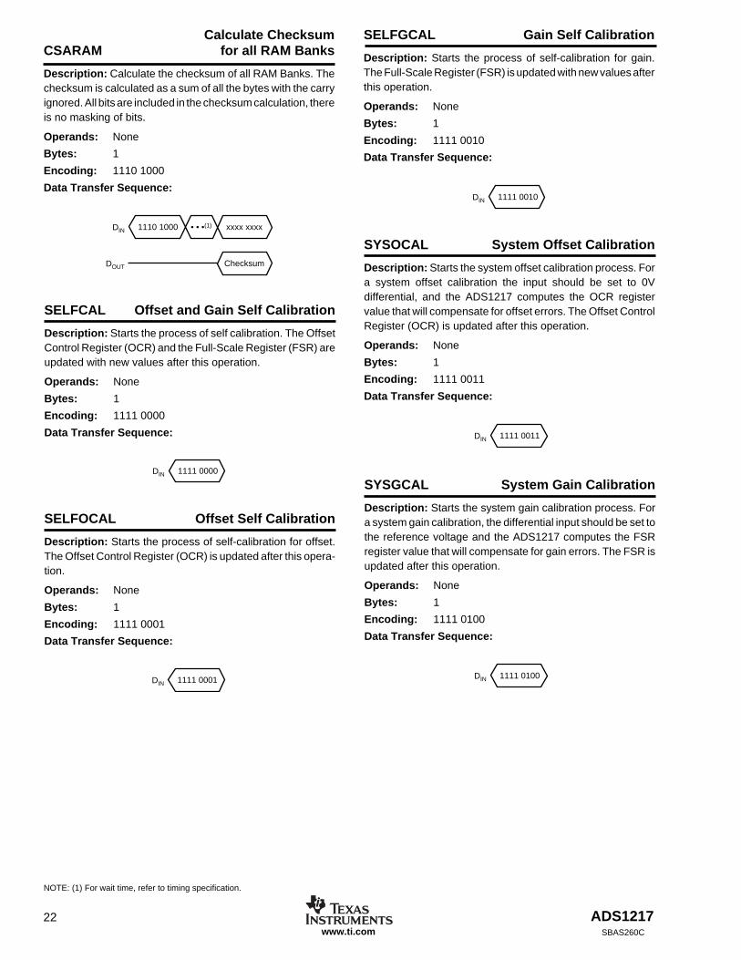
ADS121722SBAS260Cwww.ti.com
SELFCAL Offset and Gain Self Calibration
Description: Starts the process of self calibration. The OffsetControl Register (OCR) and the Full-Scale Register (FSR) areupdated with new values after this operation.
Operands: None
Bytes: 1
Encoding: 1111 0000
Data Transfer Sequence:
SELFOCAL Offset Self Calibration
Description: Starts the process of self-calibration for offset.The Offset Control Register (OCR) is updated after this opera-tion.
Operands: None
Bytes: 1
Encoding: 1111 0001
Data Transfer Sequence:
SELFGCAL Gain Self Calibration
Description: Starts the process of self-calibration for gain.The Full-Scale Register (FSR) is updated with new values afterthis operation.
Operands: None
Bytes: 1
Encoding: 1111 0010
Data Transfer Sequence:
SYSOCAL System Offset Calibration
Description: Starts the system offset calibration process. Fora system offset calibration the input should be set to 0Vdifferential, and the ADS1217 computes the OCR registervalue that will compensate for offset errors. The Offset ControlRegister (OCR) is updated after this operation.
Operands: None
Bytes: 1
Encoding: 1111 0011
Data Transfer Sequence:
SYSGCAL System Gain Calibration
Description: Starts the system gain calibration process. Fora system gain calibration, the differential input should be set tothe reference voltage and the ADS1217 computes the FSRregister value that will compensate for gain errors. The FSR isupdated after this operation.
Operands: None
Bytes: 1
Encoding: 1111 0100
Data Transfer Sequence:
Calculate ChecksumCSARAM for all RAM Banks
Description: Calculate the checksum of all RAM Banks. Thechecksum is calculated as a sum of all the bytes with the carryignored. All bits are included in the checksum calculation, thereis no masking of bits.
Operands: None
Bytes: 1
Encoding: 1110 1000
Data Transfer Sequence:
DIN 1110 1000 • • •(1) xxxx xxxx
DOUT Checksum
DIN 1111 0000
DIN 1111 0001
DIN 1111 0010
DIN 1111 0011
DIN 1111 0100
NOTE: (1) For wait time, refer to timing specification.

ADS1217SBAS260C
23www.ti.com
LSB
MSB 0000 0001 0010 0011 0100 0101 0110 0111 1000 1001 1010 1011 1100 1101 1110 1111
0000 x rdata x rdatac x x x x x x x x x x x stopc
0001 rreg rreg rreg rreg rreg rreg rreg rreg rreg rreg rreg rreg rreg rreg rreg rreg0 1 2 3 4 5 6 7 8 9 A B C D E F
0010 rram rram rram rram rram rram rram rram x x x x x x x x0 1 2 3 4 5 6 7
0011 x x x x x x x x x x x x x x x x
0100 creg creg creg creg creg creg creg creg crega x x x x x x x0 1 2 3 4 5 6 7
0101 wreg wreg wreg wreg wreg wreg wreg wreg wreg wreg wreg wreg wreg wreg wreg wreg0 1 2 3 4 5 6 7 8 9 A B C D E F
0110 wram wram wram wram wram wram wram wram x x x x x x x x0 1 2 3 4 5 6 7
0111 x x x x x x x x x x x x x x x x
1000 x x x x x x x x x x x x x x x x
1001 x x x x x x x x x x x x x x x x
1010 x x x x x x x x x x x x x x x x
1011 x x x x x x x x x x x x x x x x
1100 cram 0 cram 1 cram 2 cram 3 cram 4 cram 5 cram 6 cram 7 x x x x x x x x
1101 csramx csramx csramx csramx csramx csramx csramx csramx csa x x x x x x0 1 2 3 4 5 6 7 ramx csreg
1110 cs cs cs cs cs cs cs cs csa x x x x x x xram 0 ram 1 ram2 ram 3 ram 4 ram 5 ram 6 ram 7 ram
1111 self self self sys sys x x x x x x wakeup dsync sleep reset xcal ocal gcal ocal gcal
x = Reserved
TABLE IV. Command Map.
SLEEP Sleep Mode
Description: Puts the ADS1217 into a low power sleep mode.SCLK must be inactive while in sleep mode. To exit this mode,issue the WAKEUP command.
Operands: None
Bytes: 1
Encoding: 1111 1101
Data Transfer Sequence:
WAKEUP Wakeup From Sleep Mode
Description: Use this command to wake up from sleep mode.
Operands: None
Bytes: 1
Encoding: 1111 1011
Data Transfer Sequence:
DSYNC Sync DRDY
Description: Synchronizes the ADS1217 to the serial clockedge.
Operands: None
Bytes: 1
Encoding: 1111 1100
Data Transfer Sequence:
DIN 1111 1100
DIN 1111 1101
DIN 1111 1011
RESET Reset to Power-Up Values
Description: Restore the registers to their power-up values.This command will also stop the Read Continuous mode. Itdoes not affect the contents of RAM.
Operands: None
Bytes: 1
Encoding: 1111 1110
Data Transfer Sequence:
DIN 1111 1110
ADS121724SBAS260Cwww.ti.com
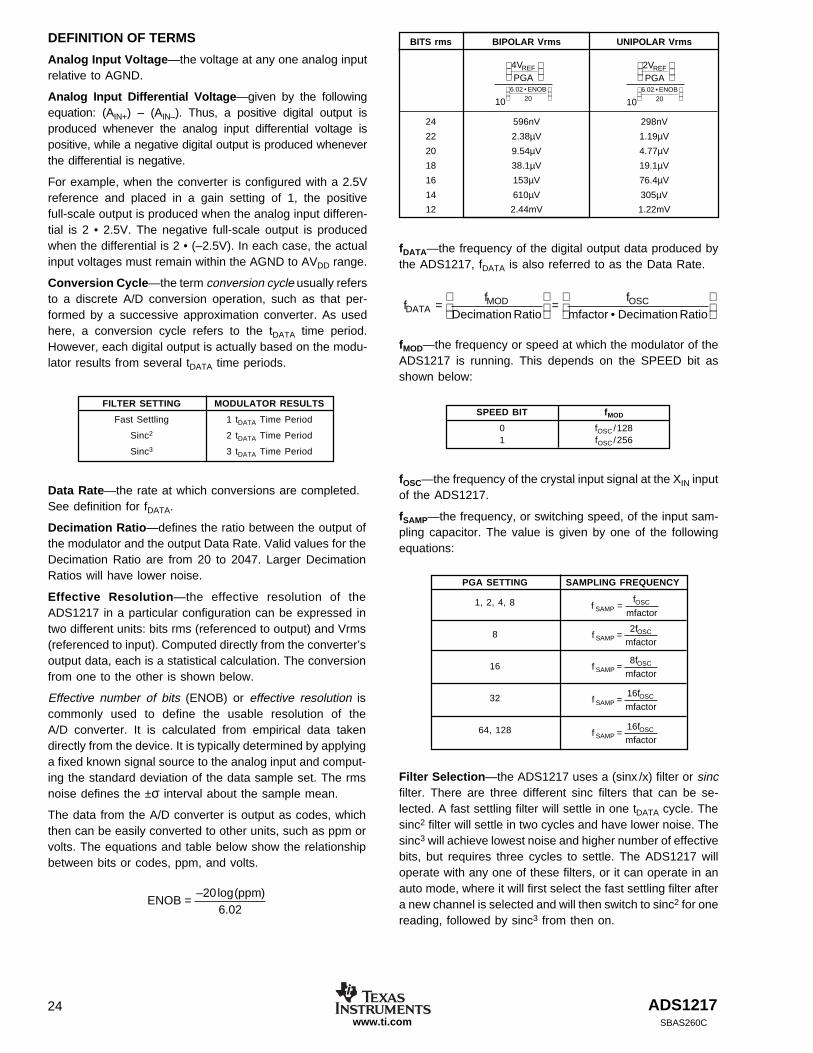
Filter Selection—the ADS1217 uses a (sinx /x) filter or sincfilter. There are three different sinc filters that can be se-lected. A fast settling filter will settle in one tDATA cycle. Thesinc2 filter will settle in two cycles and have lower noise. Thesinc3 will achieve lowest noise and higher number of effectivebits, but requires three cycles to settle. The ADS1217 willoperate with any one of these filters, or it can operate in anauto mode, where it will first select the fast settling filter aftera new channel is selected and will then switch to sinc2 for onereading, followed by sinc3 from then on.
fDATA—the frequency of the digital output data produced bythe ADS1217, fDATA is also referred to as the Data Rate.
ff
Decimation Ratiof
mfactor Decimation RatioDATAMOD OSC=
=•
fMOD—the frequency or speed at which the modulator of theADS1217 is running. This depends on the SPEED bit asshown below:
DEFINITION OF TERMS
Analog Input Voltage—the voltage at any one analog inputrelative to AGND.
Analog Input Differential Voltage—given by the followingequation: (AIN+) – (AIN–). Thus, a positive digital output isproduced whenever the analog input differential voltage ispositive, while a negative digital output is produced wheneverthe differential is negative.
For example, when the converter is configured with a 2.5Vreference and placed in a gain setting of 1, the positivefull-scale output is produced when the analog input differen-tial is 2 • 2.5V. The negative full-scale output is producedwhen the differential is 2 • (–2.5V). In each case, the actualinput voltages must remain within the AGND to AVDD range.
Conversion Cycle—the term conversion cycle usually refersto a discrete A/D conversion operation, such as that per-formed by a successive approximation converter. As usedhere, a conversion cycle refers to the tDATA time period.However, each digital output is actually based on the modu-lator results from several tDATA time periods.
FILTER SETTING MODULATOR RESULTS
Fast Settling 1 tDATA Time Period
Sinc2 2 tDATA Time Period
Sinc3 3 tDATA Time Period
BITS rms BIPOLAR Vrms UNIPOLAR Vrms
24 596nV 298nV
22 2.38µV 1.19µV
20 9.54µV 4.77µV
18 38.1µV 19.1µV
16 153µV 76.4µV
14 610µV 305µV
12 2.44mV 1.22mV
Data Rate—the rate at which conversions are completed.See definition for fDATA.
Decimation Ratio—defines the ratio between the output ofthe modulator and the output Data Rate. Valid values for theDecimation Ratio are from 20 to 2047. Larger DecimationRatios will have lower noise.
Effective Resolution—the effective resolution of theADS1217 in a particular configuration can be expressed intwo different units: bits rms (referenced to output) and Vrms(referenced to input). Computed directly from the converter’soutput data, each is a statistical calculation. The conversionfrom one to the other is shown below.
Effective number of bits (ENOB) or effective resolution iscommonly used to define the usable resolution of theA/D converter. It is calculated from empirical data takendirectly from the device. It is typically determined by applyinga fixed known signal source to the analog input and comput-ing the standard deviation of the data sample set. The rmsnoise defines the ±σ interval about the sample mean.
The data from the A/D converter is output as codes, whichthen can be easily converted to other units, such as ppm orvolts. The equations and table below show the relationshipbetween bits or codes, ppm, and volts.
ENOBppm= – log( )
.20
6 02
SPEED BIT fMOD
0 fOSC /1281 fOSC /256
fOSC—the frequency of the crystal input signal at the XIN inputof the ADS1217.
fSAMP—the frequency, or switching speed, of the input sam-pling capacitor. The value is given by one of the followingequations:
PGA SETTING SAMPLING FREQUENCY
1, 2, 4, 8
8
16
32
64, 128
ff
mfactorSAMPOSC=
ff
mfactorSAMPOSC=
2
ff
mfactorSAMPOSC=
8
ff
mfactorSAMPOSC=
16
ff
mfactorSAMPOSC=
16
4
106 02
20
VPGA
REF
ENOB
. •
2
106 02
20
VPGA
REF
ENOB
. •
ADS1217SBAS260C
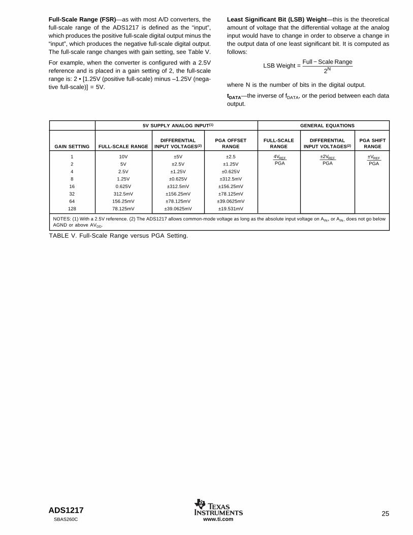
25www.ti.com
±V
PGAREF
5V SUPPLY ANALOG INPUT(1) GENERAL EQUATIONS
DIFFERENTIAL PGA OFFSET FULL-SCALE DIFFERENTIAL PGA SHIFTGAIN SETTING FULL-SCALE RANGE INPUT VOLTAGES(2) RANGE RANGE INPUT VOLTAGES(2) RANGE
1 10V ±5V ±2.5
2 5V ±2.5V ±1.25V
4 2.5V ±1.25V ±0.625V
8 1.25V ±0.625V ±312.5mV
16 0.625V ±312.5mV ±156.25mV
32 312.5mV ±156.25mV ±78.125mV
64 156.25mV ±78.125mV ±39.0625mV
128 78.125mV ±39.0625mV ±19.531mV
NOTES: (1) With a 2.5V reference. (2) The ADS1217 allows common-mode voltage as long as the absolute input voltage on AIN+ or AIN– does not go belowAGND or above AVDD.
TABLE V. Full-Scale Range versus PGA Setting.
Full-Scale Range (FSR)—as with most A/D converters, thefull-scale range of the ADS1217 is defined as the “input”,which produces the positive full-scale digital output minus the“input”, which produces the negative full-scale digital output.The full-scale range changes with gain setting, see Table V.
For example, when the converter is configured with a 2.5Vreference and is placed in a gain setting of 2, the full-scalerange is: 2 • [1.25V (positive full-scale) minus –1.25V (nega-tive full-scale)] = 5V.
Least Significant Bit (LSB) Weight—this is the theoreticalamount of voltage that the differential voltage at the analoginput would have to change in order to observe a change inthe output data of one least significant bit. It is computed asfollows:
LSB WeightFull Scale Range
N= −2
where N is the number of bits in the digital output.
tDATA—the inverse of fDATA, or the period between each dataoutput.
4VPGA
REF ±2VPGA
REF
ADS121726SBAS260Cwww.ti.com
DATE REVISION PAGE SECTION DESCRIPTION
2/07 C 2,4 Electrical Characteristics Changed Gain Error condition from “Before Calibration” to “After Calibration”
NOTE: Page numbers for previous revisions may differ from page numbers in the current version.
Revision History

PACKAGE OPTION ADDENDUM
www.ti.com 10-Jun-2014
Addendum-Page 1
PACKAGING INFORMATION
Orderable Device Status(1)
Package Type PackageDrawing
Pins PackageQty
Eco Plan(2)
Lead/Ball Finish(6)
MSL Peak Temp(3)
Op Temp (°C) Device Marking(4/5)
Samples
ADS1217IPFBR ACTIVE TQFP PFB 48 2000 Green (RoHS& no Sb/Br)
CU NIPDAU Level-2-260C-1 YEAR -40 to 85 ADS1217
ADS1217IPFBT ACTIVE TQFP PFB 48 250 Green (RoHS& no Sb/Br)
CU NIPDAU Level-2-260C-1 YEAR -40 to 85 ADS1217
ADS1217IPFBTG4 ACTIVE TQFP PFB 48 250 Green (RoHS& no Sb/Br)
CU NIPDAU Level-2-260C-1 YEAR -40 to 85 ADS1217
(1) The marketing status values are defined as follows:ACTIVE: Product device recommended for new designs.LIFEBUY: TI has announced that the device will be discontinued, and a lifetime-buy period is in effect.NRND: Not recommended for new designs. Device is in production to support existing customers, but TI does not recommend using this part in a new design.PREVIEW: Device has been announced but is not in production. Samples may or may not be available.OBSOLETE: TI has discontinued the production of the device.
(2) Eco Plan - The planned eco-friendly classification: Pb-Free (RoHS), Pb-Free (RoHS Exempt), or Green (RoHS & no Sb/Br) - please check http://www.ti.com/productcontent for the latest availabilityinformation and additional product content details.TBD: The Pb-Free/Green conversion plan has not been defined.Pb-Free (RoHS): TI's terms "Lead-Free" or "Pb-Free" mean semiconductor products that are compatible with the current RoHS requirements for all 6 substances, including the requirement thatlead not exceed 0.1% by weight in homogeneous materials. Where designed to be soldered at high temperatures, TI Pb-Free products are suitable for use in specified lead-free processes.Pb-Free (RoHS Exempt): This component has a RoHS exemption for either 1) lead-based flip-chip solder bumps used between the die and package, or 2) lead-based die adhesive used betweenthe die and leadframe. The component is otherwise considered Pb-Free (RoHS compatible) as defined above.Green (RoHS & no Sb/Br): TI defines "Green" to mean Pb-Free (RoHS compatible), and free of Bromine (Br) and Antimony (Sb) based flame retardants (Br or Sb do not exceed 0.1% by weightin homogeneous material)
(3) MSL, Peak Temp. - The Moisture Sensitivity Level rating according to the JEDEC industry standard classifications, and peak solder temperature.
(4) There may be additional marking, which relates to the logo, the lot trace code information, or the environmental category on the device.
(5) Multiple Device Markings will be inside parentheses. Only one Device Marking contained in parentheses and separated by a "~" will appear on a device. If a line is indented then it is a continuationof the previous line and the two combined represent the entire Device Marking for that device.
(6) Lead/Ball Finish - Orderable Devices may have multiple material finish options. Finish options are separated by a vertical ruled line. Lead/Ball Finish values may wrap to two lines if the finishvalue exceeds the maximum column width.
Important Information and Disclaimer:The information provided on this page represents TI's knowledge and belief as of the date that it is provided. TI bases its knowledge and belief on informationprovided by third parties, and makes no representation or warranty as to the accuracy of such information. Efforts are underway to better integrate information from third parties. TI has taken and

PACKAGE OPTION ADDENDUM
www.ti.com 10-Jun-2014
Addendum-Page 2
continues to take reasonable steps to provide representative and accurate information but may not have conducted destructive testing or chemical analysis on incoming materials and chemicals.TI and TI suppliers consider certain information to be proprietary, and thus CAS numbers and other limited information may not be available for release.
In no event shall TI's liability arising out of such information exceed the total purchase price of the TI part(s) at issue in this document sold by TI to Customer on an annual basis.

TAPE AND REEL INFORMATION
*All dimensions are nominal
Device PackageType
PackageDrawing
Pins SPQ ReelDiameter
(mm)
ReelWidth
W1 (mm)
A0(mm)
B0(mm)
K0(mm)
P1(mm)
W(mm)
Pin1Quadrant
ADS1217IPFBR TQFP PFB 48 2000 330.0 16.4 9.6 9.6 1.5 12.0 16.0 Q2
ADS1217IPFBT TQFP PFB 48 250 180.0 16.4 9.6 9.6 1.5 12.0 16.0 Q2
PACKAGE MATERIALS INFORMATION
www.ti.com 7-Feb-2015
Pack Materials-Page 1

*All dimensions are nominal
Device Package Type Package Drawing Pins SPQ Length (mm) Width (mm) Height (mm)
ADS1217IPFBR TQFP PFB 48 2000 367.0 367.0 38.0
ADS1217IPFBT TQFP PFB 48 250 213.0 191.0 55.0
PACKAGE MATERIALS INFORMATION
www.ti.com 7-Feb-2015
Pack Materials-Page 2

MECHANICAL DATA
MTQF019A – JANUARY 1995 – REVISED JANUARY 1998
POST OFFICE BOX 655303 • DALLAS, TEXAS 75265
PFB (S-PQFP-G48) PLASTIC QUAD FLATPACK
4073176/B 10/96
Gage Plane
0,13 NOM
0,25
0,450,75
Seating Plane
0,05 MIN
0,170,27
24
25
13
12
SQ
36
37
7,206,80
48
1
5,50 TYP
SQ8,809,20
1,050,95
1,20 MAX0,08
0,50 M0,08
0°–7°
NOTES: A. All linear dimensions are in millimeters.B. This drawing is subject to change without notice.C. Falls within JEDEC MS-026

IMPORTANT NOTICE
Texas Instruments Incorporated and its subsidiaries (TI) reserve the right to make corrections, enhancements, improvements and otherchanges to its semiconductor products and services per JESD46, latest issue, and to discontinue any product or service per JESD48, latestissue. Buyers should obtain the latest relevant information before placing orders and should verify that such information is current andcomplete. All semiconductor products (also referred to herein as “components”) are sold subject to TI’s terms and conditions of salesupplied at the time of order acknowledgment.TI warrants performance of its components to the specifications applicable at the time of sale, in accordance with the warranty in TI’s termsand conditions of sale of semiconductor products. Testing and other quality control techniques are used to the extent TI deems necessaryto support this warranty. Except where mandated by applicable law, testing of all parameters of each component is not necessarilyperformed.TI assumes no liability for applications assistance or the design of Buyers’ products. Buyers are responsible for their products andapplications using TI components. To minimize the risks associated with Buyers’ products and applications, Buyers should provideadequate design and operating safeguards.TI does not warrant or represent that any license, either express or implied, is granted under any patent right, copyright, mask work right, orother intellectual property right relating to any combination, machine, or process in which TI components or services are used. Informationpublished by TI regarding third-party products or services does not constitute a license to use such products or services or a warranty orendorsement thereof. Use of such information may require a license from a third party under the patents or other intellectual property of thethird party, or a license from TI under the patents or other intellectual property of TI.Reproduction of significant portions of TI information in TI data books or data sheets is permissible only if reproduction is without alterationand is accompanied by all associated warranties, conditions, limitations, and notices. TI is not responsible or liable for such altereddocumentation. Information of third parties may be subject to additional restrictions.Resale of TI components or services with statements different from or beyond the parameters stated by TI for that component or servicevoids all express and any implied warranties for the associated TI component or service and is an unfair and deceptive business practice.TI is not responsible or liable for any such statements.Buyer acknowledges and agrees that it is solely responsible for compliance with all legal, regulatory and safety-related requirementsconcerning its products, and any use of TI components in its applications, notwithstanding any applications-related information or supportthat may be provided by TI. Buyer represents and agrees that it has all the necessary expertise to create and implement safeguards whichanticipate dangerous consequences of failures, monitor failures and their consequences, lessen the likelihood of failures that might causeharm and take appropriate remedial actions. Buyer will fully indemnify TI and its representatives against any damages arising out of the useof any TI components in safety-critical applications.In some cases, TI components may be promoted specifically to facilitate safety-related applications. With such components, TI’s goal is tohelp enable customers to design and create their own end-product solutions that meet applicable functional safety standards andrequirements. Nonetheless, such components are subject to these terms.No TI components are authorized for use in FDA Class III (or similar life-critical medical equipment) unless authorized officers of the partieshave executed a special agreement specifically governing such use.Only those TI components which TI has specifically designated as military grade or “enhanced plastic” are designed and intended for use inmilitary/aerospace applications or environments. Buyer acknowledges and agrees that any military or aerospace use of TI componentswhich have not been so designated is solely at the Buyer's risk, and that Buyer is solely responsible for compliance with all legal andregulatory requirements in connection with such use.TI has specifically designated certain components as meeting ISO/TS16949 requirements, mainly for automotive use. In any case of use ofnon-designated products, TI will not be responsible for any failure to meet ISO/TS16949.
Products ApplicationsAudio www.ti.com/audio Automotive and Transportation www.ti.com/automotiveAmplifiers amplifier.ti.com Communications and Telecom www.ti.com/communicationsData Converters dataconverter.ti.com Computers and Peripherals www.ti.com/computersDLP® Products www.dlp.com Consumer Electronics www.ti.com/consumer-appsDSP dsp.ti.com Energy and Lighting www.ti.com/energyClocks and Timers www.ti.com/clocks Industrial www.ti.com/industrialInterface interface.ti.com Medical www.ti.com/medicalLogic logic.ti.com Security www.ti.com/securityPower Mgmt power.ti.com Space, Avionics and Defense www.ti.com/space-avionics-defenseMicrocontrollers microcontroller.ti.com Video and Imaging www.ti.com/videoRFID www.ti-rfid.comOMAP Applications Processors www.ti.com/omap TI E2E Community e2e.ti.comWireless Connectivity www.ti.com/wirelessconnectivity
Mailing Address: Texas Instruments, Post Office Box 655303, Dallas, Texas 75265Copyright © 2015, Texas Instruments Incorporated