8-Bit AVR Microcontroller With 2Kb of in-System Programmable Flash
Features• High Performance, Low Power AVR® 8-Bit Microcontroller• Advanced RISC Architecture
– 135 Powerful Instructions – Most Single Clock Cycle Execution– 32 x 8 General Purpose Working Registers– Fully Static Operation– Up to 16 MIPS Throughput at 16 MHz– On-Chip 2-cycle Multiplier
• Non-volatile Program and Data Memories– 16/32K Bytes of In-System Self-Programmable Flash
• Endurance: 100,000 Write/Erase Cycles– Optional Boot Code Section with Independent Lock Bits
• In-System Programming by On-chip Boot Program hardware activated after reset
• True Read-While-Write Operation• All supplied parts are preprogramed with a default USB bootloader
– 1.25/2.5K Bytes Internal SRAM– 512Bytes/1K Bytes Internal EEPROM
• Endurance: 100,000 Write/Erase Cycles– Programming Lock for Software Security
• JTAG (IEEE std. 1149.1 compliant) Interface– Boundary-scan Capabilities According to the JTAG Standard– Extensive On-chip Debug Support– Programming of Flash, EEPROM, Fuses, and Lock Bits through the JTAG Interface
• USB 2.0 Full-speed/Low Speed Device Module with Interrupt on Transfer Completion– Complies fully with Universal Serial Bus Specification Rev 2.0– Supports data transfer rates up to 12 Mbit/s and 1.5 Mbit/s– Endpoint 0 for Control Transfers: up to 64-bytes– 6 Programmable Endpoints with IN or Out Directions and with Bulk, Interrupt or
Isochronous Transfers– Configurable Endpoints size up to 256 bytes in double bank mode– Fully independent 832 bytes USB DPRAM for endpoint memory allocation– Suspend/Resume Interrupts– CPU Reset possible on USB Bus Reset detection– 48 MHz from PLL for Full-speed Bus Operation– USB Bus Connection/Disconnection on Microcontroller Request
• Peripheral Features– On-chip PLL for USB and High Speed Timer: 32 up to 96 MHz operation– Two 8-bit Timer/Counters with Separate Prescaler and Compare Mode– Two 16-bit Timer/Counter with Separate Prescaler, Compare- and Capture Mode– One 10-bit High-Speed Timer/Counter with PLL (64 MHz) and Compare Mode– Four 8-bit PWM Channels– Four PWM Channels with Programmable Resolution from 2 to 16 Bits– Six PWM Channels for High Speed Operation, with Programmable Resolution from
2 to 11 Bits– Output Compare Modulator– 12-channels, 10-bit ADC (features Differential Channels with Programmable Gain)– Programmable Serial USART with Hardware Flow Control– Master/Slave SPI Serial Interface
http://www.xinpian.net 提供单片机解密、IC解密、芯片解密业务
8-bit Microcontroller with16/32K Bytes of ISP Flashand USB Controller
ATmega16U4ATmega32U4
Preliminary
Summary
7766BS–AVR–07/08
010-62245566 13810019655
– Byte Oriented 2-wire Serial Interface– Programmable Watchdog Timer with Separate On-chip Oscillator– On-chip Analog Comparator– Interrupt and Wake-up on Pin Change (8xPCINT + 5xINT sources)– On-chip Temperature Sensor (see A/D Converter section)
• Special Microcontroller Features– Power-on Reset and Programmable Brown-out Detection– Internal 8 MHz Calibrated Oscillator– Internal clock prescaler & On-the-fly Clock Switching (Int RC / Ext Osc)– External and Internal Interrupt Sources– Six Sleep Modes: Idle, ADC Noise Reduction, Power-save, Power-down, Standby, and Extended Standby
• I/O and Packages– All I/O combine CMOS outputs and LVTTL inputs– 26 Programmable I/O Lines– 44-lead TQFP Package, 10x10mm– 44-lead QFN Package, 7x7mm
• Operating Voltages– 2.7 - 5.5V
• Operating temperature– Industrial (-40°C to +85°C)
• Maximum Frequency– 8 MHz at 2.7V - Industrial range– 16 MHz at 4.5V - Industrial range
27766BS–AVR–07/08
ATmega16U4/ATmega32U4http://www.xinpian.net 提供单片机解密、IC解密、芯片解密业务 010-62245566 13810019655
ATmega16U4/ATmega32U4
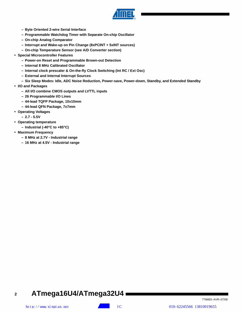
1. Pin Configurations
7766BS–AVR–07/08
http://www.xinpi
Figure 1-1. Pinout ATmega16U4/ATmega32U4
1.1 Disclaimer
AT90USB32444-pin QFN/TQFP
UVcc
D-
D+
UGnd
UCap
VBus
(SS/PCINT0) PB0
(INT.6/AIN.0) PE6
(PCINT1/SCLK) PB1
(PDI/PCINT2/MOSI) PB2
(PDO/PCINT3/MISO) PB3
(PC
INT
7/O
C0A
/OC
1C/R
TS
) P
B7
RE
SE
T
VC
C
GN
D
XTA
L2
XTA
L1
(OC
0B/S
CL/
INT
0) P
D0
(OC
2B/S
DA
/INT
1) P
D1
(RX
D1/
INT
2) P
D2
(TX
D1/
INT
3) P
D3
(XC
K1/
CT
S)
PD
5
PE2 (HWB)
PC7 (ICP3/CLK0/OC4A)
PC6 (OC3A/OC4A)
PB6 (PCINT6/OC1B/OC4B/ADC13)
PB4 (PCINT4/OC2A/ADC11)
PD7 (T0/OC4D/ADC10)
PD6 (T1/OC4D/ADC9)
PD4 (ICP1/ADC8)
AV
CC
GN
D
AR
EF
PF
0 (A
DC
0)
PF
1 (A
DC
1)
PF
4 (A
DC
4/T
CK
)
PF
5 (A
DC
5/T
MS
)
PF
6 (A
DC
6/T
DO
)
PF
7 (A
DC
7/T
DI)
GN
D
VC
C
INDEX CORNER
1
2
3
4
5
6
7
8
9
10
11
33
32
31
30
29
28
27
26
25
24
23
12 13 14 15 16 17 18 19 20 21 22
44 43 42 41 40 39 38 37 36 35 34
PB5 (PCINT5/OC1A/OC4B/ADC12)
AVCC
GND
Typical values contained in this datasheet are based on simulations and characterization ofother AVR microcontrollers manufactured on the same process technology. Min and Max valueswill be available after the device is characterized.
2. Overview
The ATmega16U4/ATmega32U4 is a low-power CMOS 8-bit microcontroller based on the AVRenhanced RISC architecture. By executing powerful instructions in a single clock cycle, theATmega16U4/ATmega32U4 achieves throughputs approaching 1 MIPS per MHz allowing thesystem designer to optimize power consumption versus processing speed.3
an.net 提供单片机解密、IC解密、芯片解密业务 010-62245566 13810019655

2.1 Block Diagram
Figure 2-1. Block Diagram
PROGRAMCOUNTER
STACKPOINTER
PROGRAMFLASH
MCU CONTROLREGISTER
GENERALPURPOSE
REGISTERS
INSTRUCTIONREGISTER
TIMERS/COUNTERS
INSTRUCTIONDECODER
DATA DIR.REG. PORTB
DATA DIR.REG. PORTE
DATA DIR.REG. PORTD
DATA REGISTERPORTB
DATA REGISTERPORTE
DATA REGISTERPORTD
INTERRUPTUNIT
EEPROM
SPI
STATUSREGISTER
SRAM
USART0
Z
Y
X
ALU
PORTB DRIVERSPORTE DRIVERS
PORTF DRIVERS
PORTD DRIVERS
PORTC DRIVERS
PB7 - PB0PE6
PF7 - PF4
RES
ET
VCC
GND
XTAL
1
XTAL
2
CONTROLLINES
PC7
INTERNALOSCILLATOR
WATCHDOGTIMER
8-BIT DA TA BUS
USB 2.0
TIMING ANDCONTROL
OSCILLATOR
CALIB. OSC
DATA DIR.REG. PORTC
DATA REGISTERPORTC
ON-CHIP DEBUG
JTAG TAP
PROGRAMMINGLOGIC
BOUNDARY- SCAN
DATA DIR.REG. PORTF
DATA REGISTERPORTF
POR - BODRESET
PD7 - PD0
TWO-WIRE SERIALINTERFACE
PLL
- Subject to changes -
HIGH SPEED
TIMER/PWM
PE2
PC6PF1 PF0
ON-CHIPUSB PAD 3VREGULATOR
UVcc
UCap
1uF
ANALOG
COMPARATOR
VBUS
DP
DM
ADCAGND
AREF
AVCC
TEMPERATURESENSOR
4 ATmegahttp://www.xinpi
The AVR core combines a rich instruction set with 32 general purpose working registers. All the32 registers are directly connected to the Arithmetic Logic Unit (ALU), allowing two independentregisters to be accessed in one single instruction executed in one clock cycle. The resultingarchitecture is more code efficient while achieving throughputs up to ten times faster than con-ventional CISC microcontrollers.
The ATmega16U4/ATmega32U4 provides the following features: 16/32K bytes of In-SystemProgrammable Flash with Read-While-Write capabilities, 512Bytes/1K bytes EEPROM,1.25/2.5K bytes SRAM, 26 general purpose I/O lines (CMOS outputs and LVTTL inputs), 32general purpose working registers, four flexible Timer/Counters with compare modes and PWM,one more high-speed Timer/Counter with compare modes and PLL adjustable source, oneUSART (including CTS/RTS flow control signals), a byte oriented 2-wire Serial Interface, a 12-
7766BS–AVR–07/08
16U4/ATmega32U4an.net 提供单片机解密、IC解密、芯片解密业务 010-62245566 13810019655

7766BS–AVR–07/08
ATmega16U4/ATmega32U4
http://www.xinpi
channels 10-bit ADC with optional differential input stage with programmable gain, an on-chipcalibrated temperature sensor, a programmable Watchdog Timer with Internal Oscillator, an SPIserial port, IEEE std. 1149.1 compliant JTAG test interface, also used for accessing the On-chipDebug system and programming and six software selectable power saving modes. The Idlemode stops the CPU while allowing the SRAM, Timer/Counters, SPI port, and interrupt systemto continue functioning. The Power-down mode saves the register contents but freezes theOscillator, disabling all other chip functions until the next interrupt or Hardware Reset. The ADCNoise Reduction mode stops the CPU and all I/O modules except ADC, to minimize switchingnoise during ADC conversions. In Standby mode, the Crystal/Resonator Oscillator is runningwhile the rest of the device is sleeping. This allows very fast start-up combined with low powerconsumption.
The device is manufactured using ATMEL’s high-density nonvolatile memory technology. TheOn-chip ISP Flash allows the program memory to be reprogrammed in-system through an SPIserial interface, by a conventional nonvolatile memory programmer, or by an On-chip Boot pro-gram running on the AVR core. The boot program can use any interface to download theapplication program in the application Flash memory. Software in the Boot Flash section willcontinue to run while the Application Flash section is updated, providing true Read-While-Writeoperation. By combining an 8-bit RISC CPU with In-System Self-Programmable Flash on amonolithic chip, the ATMEL ATmega16U4/ATmega32U4 is a powerful microcontroller that pro-vides a highly flexible and cost effective solution to many embedded control applications.
The ATmega16U4/ATmega32U4 AVR is supported with a full suite of program and systemdevelopment tools including: C compilers, macro assemblers, program debugger/simulators, in-circuit emulators, and evaluation kits.
2.2 Pin Descriptions
2.2.1 VCC
Digital supply voltage.2.2.2 GND
Ground.2.2.3 Port B (PB7..PB0)
Port B is an 8-bit bi-directional I/O port with internal pull-up resistors (selected for each bit). ThePort B output buffers have symmetrical drive characteristics with both high sink and sourcecapability. As inputs, Port B pins that are externally pulled low will source current if the pull-upresistors are activated. The Port B pins are tri-stated when a reset condition becomes active,even if the clock is not running.Port B has better driving capabilities than the other ports.
Port B also serves the functions of various special features of the ATmega16U4/ATmega32U4as listed on page 70.
2.2.4 Port C (PC7,PC6)
Port C is an 8-bit bi-directional I/O port with internal pull-up resistors (selected for each bit). ThePort C output buffers have symmetrical drive characteristics with both high sink and sourcecapability. As inputs, Port C pins that are externally pulled low will source current if the pull-upresistors are activated. The Port C pins are tri-stated when a reset condition becomes active,even if the clock is not running.5
an.net 提供单片机解密、IC解密、芯片解密业务 010-62245566 13810019655
6 ATmegahttp://www.xinpi
Only bits 6 and 7 are present on the product pinout.
Port C also serves the functions of special features of the ATmega16U4/ATmega32U4 as listedon page 73.
2.2.5 Port D (PD7..PD0)
Port D is an 8-bit bi-directional I/O port with internal pull-up resistors (selected for each bit). ThePort D output buffers have symmetrical drive characteristics with both high sink and sourcecapability. As inputs, Port D pins that are externally pulled low will source current if the pull-upresistors are activated. The Port D pins are tri-stated when a reset condition becomes active,even if the clock is not running.Port D also serves the functions of various special features of the ATmega16U4/ATmega32U4as listed on page 75.
2.2.6 Port E (PE6,PE2)
Port E is an 8-bit bi-directional I/O port with internal pull-up resistors (selected for each bit). ThePort E output buffers have symmetrical drive characteristics with both high sink and sourcecapability. As inputs, Port E pins that are externally pulled low will source current if the pull-upresistors are activated. The Port E pins are tri-stated when a reset condition becomes active,even if the clock is not running.Only bits 2 and 6 are present on the product pinout.
Port E also serves the functions of various special features of the ATmega16U4/ATmega32U4as listed on page 78.
2.2.7 Port F (PF7..PF4, PF1,PF0)
Port F serves as analog inputs to the A/D Converter.Port F also serves as an 8-bit bi-directional I/O port, if the A/D Converter channels are not used.Port pins can provide internal pull-up resistors (selected for each bit). The Port F output buffershave symmetrical drive characteristics with both high sink and source capability. As inputs, PortF pins that are externally pulled low will source current if the pull-up resistors are activated. ThePort F pins are tri-stated when a reset condition becomes active, even if the clock is not running.
Bits 2 and 3 are not present on the product pinout.
Port F also serves the functions of the JTAG interface. If the JTAG interface is enabled, the pull-up resistors on pins PF7(TDI), PF5(TMS), and PF4(TCK) will be activated even if a reset occurs.
2.2.8 D-
USB Full speed / Low Speed Negative Data Upstream Port. Should be connected to the USB D-connector pin with a serial 22 Ohms resistor.2.2.9 D+
USB Full speed / Low Speed Positive Data Upstream Port. Should be connected to the USB D+connector pin with a serial 22 Ohms resistor.2.2.10 UGND
USB Pads Ground.7766BS–AVR–07/08
16U4/ATmega32U4an.net 提供单片机解密、IC解密、芯片解密业务 010-62245566 13810019655
ATmega16U4/ATmega32U4
2.2.11 UVCC
7766BS–AVR–07/08
http://www.xinpi
USB Pads Internal Regulator Input supply voltage.
2.2.12 UCAP
USB Pads Internal Regulator Output supply voltage. Should be connected to an external capac-itor (1µF).2.2.13 VBUS
USB VBUS monitor input.2.2.14 RESET
Reset input. A low level on this pin for longer than the minimum pulse length will generate areset, even if the clock is not running. The minimum pulse length is given in Table 8-1 on page48. Shorter pulses are not guaranteed to generate a reset.2.2.15 XTAL1
Input to the inverting Oscillator amplifier and input to the internal clock operating circuit.2.2.16 XTAL2
Output from the inverting Oscillator amplifier.2.2.17 AVCC
AVCC is the supply voltage pin (input) for all the A/D Converter channels. If the ADC is not used,it should be externally connected to VCC. If the ADC is used, it should be connected to VCCthrough a low-pass filter.2.2.18 AREF
This is the analog reference pin (input) for the A/D Converter.3. About Code Examples
This documentation contains simple code examples that briefly show how to use various parts ofthe device. Be aware that not all C compiler vendors include bit definitions in the header filesand interrupt handling in C is compiler dependent. Please confirm with the C compiler documen-tation for more details.These code examples assume that the part specific header file is included before compilation.For I/O registers located in extended I/O map, "IN", "OUT", "SBIS", "SBIC", "CBI", and "SBI"instructions must be replaced with instructions that allow access to extended I/O. Typically"LDS" and "STS" combined with "SBRS", "SBRC", "SBR", and "CBR".
7
an.net 提供单片机解密、IC解密、芯片解密业务 010-62245566 13810019655

8 ATmegahttp://www.xinpi
7766BS–AVR–07/08
16U4/ATmega32U4an.net 提供单片机解密、IC解密、芯片解密业务 010-62245566 13810019655
ATmega16U4/ATmega32U4
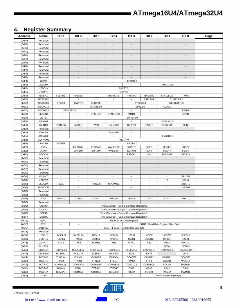
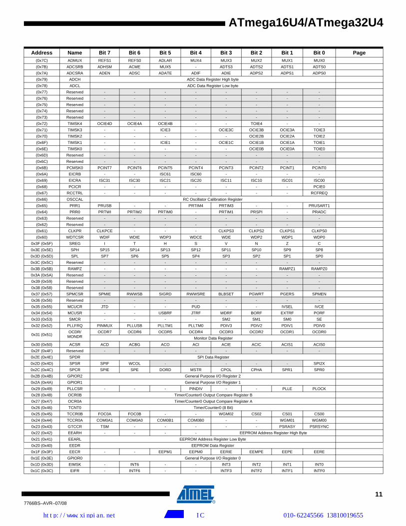
4. Register SummaryAddress Name Bit 7 Bit 6 Bit 5 Bit 4 Bit 3 Bit 2 Bit 1 Bit 0 Page
(0xFF) Reserved - - - - - - - -(0xFE) Reserved - - - - - - - -(0xFD) Reserved - - - - - - - -(0xFC) Reserved - - - - - - - -(0xFB) Reserved - - - - - - - -(0xFA) Reserved - - - - - - - -(0xF9) Reserved - - - -(0xF8) Reserved - - - - - - - -(0xF7) Reserved - - - - - - - -(0xF6) Reserved - - - - - - - -(0xF5) Reserved - - - - - - - -(0xF4) UEINT - EPINT6:0(0xF3) UEBCHX - - - - - BYCT10:8(0xF2) UEBCLX BYCT7:0(0xF1) UEDATX DAT7:0(0xF0) UEIENX FLERRE NAKINE - NAKOUTE RXSTPE RXOUTE STALLEDE TXINE(0xEF) UESTA1X - - - - - CTRLDIR CURRBK1:0(0xEE) UESTA0X CFGOK OVERFI UNDERFI - DTSEQ1:0 NBUSYBK1:0(0xED) UECFG1X EPSIZE2:0 EPBK1:0 ALLOC -(0xEC) UECFG0X EPTYPE1:0 - - - - - EPDIR(0xEB) UECONX - - STALLRQ STALLRQC RSTDT - - EPEN(0xEA) UERST - EPRST6:0(0xE9) UENUM - - - - - EPNUM2:0(0xE8) UEINTX FIFOCON NAKINI RWAL NAKOUTI RXSTPI RXOUTI STALLEDI TXINI(0xE7) Reserved - - - -(0xE6) UDMFN - - - FNCERR - - - -(0xE5) UDFNUMH - - - - - FNUM10:8(0xE4) UDFNUML FNUM7:0(0xE3) UDADDR ADDEN UADD6:0(0xE2) UDIEN - UPRSME EORSME WAKEUPE EORSTE SOFE MSOFE SUSPE(0xE1) UDINT - UPRSMI EORSMI WAKEUPI EORSTI SOFI MSOFI SUSPI(0xE0) UDCON - - - - RSTCPU LSM RMWKUP DETACH(0xDF) Reserved(0xDE) Reserved(0xDD) Reserved(0xDC) Reserved(0xDB) Reserved(0xDA) USBINT - - - - - - - VBUSTI(0xD9) USBSTA - - - - - - ID VBUS(0xD8) USBCON USBE - FRZCLK OTGPADE - - - VBUSTE(0xD7) UHWCON - - - - - - - UVREGE(0xD6) Reserved(0xD5) Reserved(0xD4) DT4 DT4H3 DT4H2 DT4H1 DT4H0 DT4L3 DT4L2 DT4L1 DT4L0(0xD3) Reserved(0xD2) OCR4D Timer/Counter4 - Output Compare Register D(0xD1) OCR4C Timer/Counter4 - Output Compare Register C(0xD0) OCR4B Timer/Counter4 - Output Compare Register B(0xCF) OCR4A Timer/Counter4 - Output Compare Register A(0xCE) UDR1 USART1 I/O Data Register(0xCD) UBRR1H - - - - USART1 Baud Rate Register High Byte(0xCC) UBRR1L USART1 Baud Rate Register Low Byte(0xCB) Reserved - - - - - - - -(0xCA) UCSR1C UMSEL11 UMSEL10 UPM11 UPM10 USBS1 UCSZ11 UCSZ10 UCPOL1(0xC9) UCSR1B RXCIE1 TXCIE1 UDRIE1 RXEN1 TXEN1 UCSZ12 RXB81 TXB81(0xC8) UCSR1A RXC1 TXC1 UDRE1 FE1 DOR1 PE1 U2X1 MPCM1(0xC7) CLKSTA - - - - - - RCON EXTON(0xC6) CLKSEL1 RCCKSEL3 RCCKSEL2 RCCKSEL1 RCCKSEL0 EXCKSEL3 EXCKSEL2 EXCKSEL1 EXCKSEL0(0xC5) CLKSEL0 RCSUT1 RCSUT0 EXSUT1 EXSUT0 RCE EXTE - CLKS(0xC4) TCCR4E TLOCK4 ENHC4 OC4OE5 OC4OE4 OC4OE3 OC4OE2 OC4OE1 OC4OE0(0xC3) TCCR4D FPIE4 FPEN4 FPNC4 FPES4 FPAC4 FPF4 WGM41 WGM40(0xC2) TCCR4C COM4A1S COM4A0S COM4B1S COM4B0S COM4D1S COM4D0S FOC4D PWM4D(0xC1) TCCR4B PWM4X PSR4 DTPS41 DTPS40 CS43 CS42 CS41 CS40(0xC0) TCCR4A COM4A1 COM4A0 COM4B1 COM4B0 FOC4A FOC4B PWM4A PWM4B(0xBF) TC4H - - - - - Timer/Counter4 High Byte
97766BS–AVR–07/08
http://www.xinpian.net 提供单片机解密、IC解密、芯片解密业务 010-62245566 13810019655
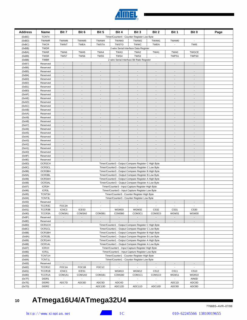
(0xBE) TCNT4 Timer/Counter4 - Counter Register Low Byte(0xBD) TWAMR TWAM6 TWAM5 TWAM4 TWAM3 TWAM2 TWAM1 TWAM0 -(0xBC) TWCR TWINT TWEA TWSTA TWSTO TWWC TWEN - TWIE(0xBB) TWDR 2-wire Serial Interface Data Register(0xBA) TWAR TWA6 TWA5 TWA4 TWA3 TWA2 TWA1 TWA0 TWGCE(0xB9) TWSR TWS7 TWS6 TWS5 TWS4 TWS3 - TWPS1 TWPS0(0xB8) TWBR 2-wire Serial Interface Bit Rate Register(0xB7) Reserved - - - - - - - -(0xB6) Reserved -(0xB5) Reserved - - - - - - - -(0xB4) Reserved - - - - - - - -(0xB3) Reserved - - - - - - - -(0xB2) Reserved - - - - - - - -(0xB1) Reserved - - - - - - - -(0xB0) Reserved - - - - - - - -(0xAF) Reserved - - - - - - - -(0xAE) Reserved - - - - - - - -(0xAD) Reserved - - - - - - - -(0xAC) Reserved - - - - - - - -(0xAB) Reserved - - - - - - - -(0xAA) Reserved - - - - - - - -(0xA9) Reserved - - - - - - - -(0xA8) Reserved - - - - - - - -(0xA7) Reserved - - - - - - - -(0xA6) Reserved - - - - - - - -(0xA5) Reserved - - - - - - - -(0xA4) Reserved - - - - - - - -(0xA3) Reserved - - - - - - - -(0xA2) Reserved - - - - - - - -(0xA1) Reserved - - - - - - - -(0xA0) Reserved - - - - - - - -(0x9F) Reserved - - - - - - - -(0x9E) Reserved - - - - - - - -(0x9D) OCR3CH Timer/Counter3 - Output Compare Register C High Byte(0x9C) OCR3CL Timer/Counter3 - Output Compare Register C Low Byte(0x9B) OCR3BH Timer/Counter3 - Output Compare Register B High Byte(0x9A) OCR3BL Timer/Counter3 - Output Compare Register B Low Byte(0x99) OCR3AH Timer/Counter3 - Output Compare Register A High Byte(0x98) OCR3AL Timer/Counter3 - Output Compare Register A Low Byte(0x97) ICR3H Timer/Counter3 - Input Capture Register High Byte(0x96) ICR3L Timer/Counter3 - Input Capture Register Low Byte(0x95) TCNT3H Timer/Counter3 - Counter Register High Byte(0x94) TCNT3L Timer/Counter3 - Counter Register Low Byte(0x93) Reserved - - - - - - - -(0x92) TCCR3C FOC3A - - - - - - -(0x91) TCCR3B ICNC3 ICES3 - WGM33 WGM32 CS32 CS31 CS30(0x90) TCCR3A COM3A1 COM3A0 COM3B1 COM3B0 COM3C1 COM3C0 WGM31 WGM30(0x8F) Reserved - - - - - - - -(0x8E) Reserved - - - - - - - -(0x8D) OCR1CH Timer/Counter1 - Output Compare Register C High Byte(0x8C) OCR1CL Timer/Counter1 - Output Compare Register C Low Byte(0x8B) OCR1BH Timer/Counter1 - Output Compare Register B High Byte (0x8A) OCR1BL Timer/Counter1 - Output Compare Register B Low Byte(0x89) OCR1AH Timer/Counter1 - Output Compare Register A High Byte(0x88) OCR1AL Timer/Counter1 - Output Compare Register A Low Byte(0x87) ICR1H Timer/Counter1 - Input Capture Register High Byte(0x86) ICR1L Timer/Counter1 - Input Capture Register Low Byte(0x85) TCNT1H Timer/Counter1 - Counter Register High Byte(0x84) TCNT1L Timer/Counter1 - Counter Register Low Byte(0x83) Reserved - - - - - - - -(0x82) TCCR1C FOC1A FOC1B FOC1C - - - - -(0x81) TCCR1B ICNC1 ICES1 - WGM13 WGM12 CS12 CS11 CS10(0x80) TCCR1A COM1A1 COM1A0 COM1B1 COM1B0 COM1C1 COM1C0 WGM11 WGM10(0x7F) DIDR1 - - - - - - - AIN0D(0x7E) DIDR0 ADC7D ADC6D ADC5D ADC4D - - ADC1D ADC0D(0x7D) DIDR2 - - ADC13D ADC12D ADC11D ADC10D ADC9D ADC8D
Address Name Bit 7 Bit 6 Bit 5 Bit 4 Bit 3 Bit 2 Bit 1 Bit 0 Page
107766BS–AVR–07/08
ATmega16U4/ATmega32U4http://www.xinpian.net 提供单片机解密、IC解密、芯片解密业务 010-62245566 13810019655
ATmega16U4/ATmega32U4
(0x7C) ADMUX REFS1 REFS0 ADLAR MUX4 MUX3 MUX2 MUX1 MUX0(0x7B) ADCSRB ADHSM ACME MUX5 - ADTS3 ADTS2 ADTS1 ADTS0(0x7A) ADCSRA ADEN ADSC ADATE ADIF ADIE ADPS2 ADPS1 ADPS0(0x79) ADCH ADC Data Register High byte(0x78) ADCL ADC Data Register Low byte(0x77) Reserved - - - - - - - -(0x76) Reserved - - - - - - - -(0x75) Reserved - - - - - - - -(0x74) Reserved - - - - - - - -(0x73) Reserved - - - - - - - -(0x72) TIMSK4 OCIE4D OCIE4A OCIE4B - - TOIE4 - -(0x71) TIMSK3 - - ICIE3 - OCIE3C OCIE3B OCIE3A TOIE3(0x70) TIMSK2 - - - - - OCIE2B OCIE2A TOIE2(0x6F) TIMSK1 - - ICIE1 - OCIE1C OCIE1B OCIE1A TOIE1(0x6E) TIMSK0 - - - - - OCIE0B OCIE0A TOIE0(0x6D) Reserved - - - - - - - -(0x6C) Reserved - - - - - - - -(0x6B) PCMSK0 PCINT7 PCINT6 PCINT5 PCINT4 PCINT3 PCINT2 PCINT1 PCINT0(0x6A) EICRB - - ISC61 ISC60 - - - -(0x69) EICRA ISC31 ISC30 ISC21 ISC20 ISC11 ISC10 ISC01 ISC00(0x68) PCICR - - - - - - - PCIE0(0x67) RCCTRL - - - - - - - RCFREQ(0x66) OSCCAL RC Oscillator Calibration Register(0x65) PRR1 PRUSB - - PRTIM4 PRTIM3 - - PRUSART1(0x64) PRR0 PRTWI PRTIM2 PRTIM0 - PRTIM1 PRSPI - PRADC(0x63) Reserved - - - - - - - -(0x62) Reserved - - - - - - - -(0x61) CLKPR CLKPCE - - - CLKPS3 CLKPS2 CLKPS1 CLKPS0(0x60) WDTCSR WDIF WDIE WDP3 WDCE WDE WDP2 WDP1 WDP0
0x3F (0x5F) SREG I T H S V N Z C0x3E (0x5E) SPH SP15 SP14 SP13 SP12 SP11 SP10 SP9 SP80x3D (0x5D) SPL SP7 SP6 SP5 SP4 SP3 SP2 SP1 SP00x3C (0x5C) Reserved - - - - - - - -0x3B (0x5B) RAMPZ - - - - - - RAMPZ1 RAMPZ00x3A (0x5A) Reserved - - - - - - - -0x39 (0x59) Reserved - - - - - - - -0x38 (0x58) Reserved - - - - - - - -0x37 (0x57) SPMCSR SPMIE RWWSB SIGRD RWWSRE BLBSET PGWRT PGERS SPMEN0x36 (0x56) Reserved - - - - - - - -0x35 (0x55) MCUCR JTD - - PUD - - IVSEL IVCE0x34 (0x54) MCUSR - - USBRF JTRF WDRF BORF EXTRF PORF0x33 (0x53) SMCR - - - - SM2 SM1 SM0 SE0x32 (0x52) PLLFRQ PINMUX PLLUSB PLLTM1 PLLTM0 PDIV3 PDIV2 PDIV1 PDIV0
0x31 (0x51)OCDR/
MONDROCDR7 OCDR6 OCDR5 OCDR4 OCDR3 OCDR2 OCDR1 OCDR0
Monitor Data Register0x30 (0x50) ACSR ACD ACBG ACO ACI ACIE ACIC ACIS1 ACIS00x2F (0x4F) Reserved - - - - - - - -0x2E (0x4E) SPDR SPI Data Register0x2D (0x4D) SPSR SPIF WCOL - - - - - SPI2X0x2C (0x4C) SPCR SPIE SPE DORD MSTR CPOL CPHA SPR1 SPR00x2B (0x4B) GPIOR2 General Purpose I/O Register 20x2A (0x4A) GPIOR1 General Purpose I/O Register 10x29 (0x49) PLLCSR - - - PINDIV - - PLLE PLOCK0x28 (0x48) OCR0B Timer/Counter0 Output Compare Register B0x27 (0x47) OCR0A Timer/Counter0 Output Compare Register A0x26 (0x46) TCNT0 Timer/Counter0 (8 Bit)0x25 (0x45) TCCR0B FOC0A FOC0B - - WGM02 CS02 CS01 CS000x24 (0x44) TCCR0A COM0A1 COM0A0 COM0B1 COM0B0 - - WGM01 WGM000x23 (0x43) GTCCR TSM - - - - - PSRASY PSRSYNC0x22 (0x42) EEARH - - - - EEPROM Address Register High Byte0x21 (0x41) EEARL EEPROM Address Register Low Byte0x20 (0x40) EEDR EEPROM Data Register0x1F (0x3F) EECR - - EEPM1 EEPM0 EERIE EEMPE EEPE EERE0x1E (0x3E) GPIOR0 General Purpose I/O Register 00x1D (0x3D) EIMSK - INT6 - - INT3 INT2 INT1 INT00x1C (0x3C) EIFR - INTF6 - - INTF3 INTF2 INTF1 INTF0
Address Name Bit 7 Bit 6 Bit 5 Bit 4 Bit 3 Bit 2 Bit 1 Bit 0 Page
117766BS–AVR–07/08
http://www.xinpian.net 提供单片机解密、IC解密、芯片解密业务 010-62245566 13810019655
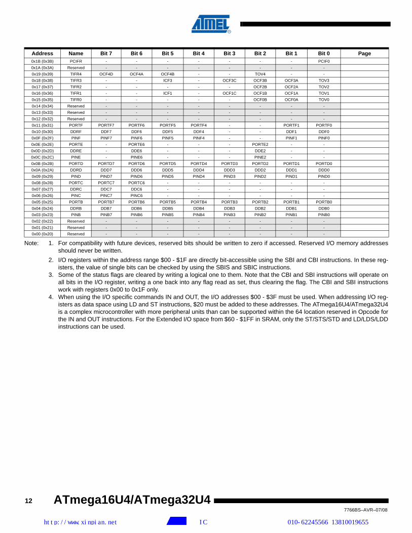
Note: 1. For compatibility with future devices, reserved bits should be written to zero if accessed. Reserved I/O memory addressesshould never be written.
2. I/O registers within the address range $00 - $1F are directly bit-accessible using the SBI and CBI instructions. In these reg-isters, the value of single bits can be checked by using the SBIS and SBIC instructions.
3. Some of the status flags are cleared by writing a logical one to them. Note that the CBI and SBI instructions will operate onall bits in the I/O register, writing a one back into any flag read as set, thus clearing the flag. The CBI and SBI instructionswork with registers 0x00 to 0x1F only.
4. When using the I/O specific commands IN and OUT, the I/O addresses $00 - $3F must be used. When addressing I/O reg-isters as data space using LD and ST instructions, $20 must be added to these addresses. The ATmega16U4/ATmega32U4is a complex microcontroller with more peripheral units than can be supported within the 64 location reserved in Opcode forthe IN and OUT instructions. For the Extended I/O space from $60 - $1FF in SRAM, only the ST/STS/STD and LD/LDS/LDDinstructions can be used.
0x1B (0x3B) PCIFR - - - - - - - PCIF00x1A (0x3A) Reserved - - - - - - - -0x19 (0x39) TIFR4 OCF4D OCF4A OCF4B - - TOV4 - -0x18 (0x38) TIFR3 - - ICF3 - OCF3C OCF3B OCF3A TOV30x17 (0x37) TIFR2 - - - - - OCF2B OCF2A TOV20x16 (0x36) TIFR1 - - ICF1 - OCF1C OCF1B OCF1A TOV10x15 (0x35) TIFR0 - - - - - OCF0B OCF0A TOV00x14 (0x34) Reserved - - - - - - - -0x13 (0x33) Reserved - - - - - - - -0x12 (0x32) Reserved - - - - - - - -0x11 (0x31) PORTF PORTF7 PORTF6 PORTF5 PORTF4 - - PORTF1 PORTF00x10 (0x30) DDRF DDF7 DDF6 DDF5 DDF4 - - DDF1 DDF00x0F (0x2F) PINF PINF7 PINF6 PINF5 PINF4 - - PINF1 PINF00x0E (0x2E) PORTE - PORTE6 - - - PORTE2 - -0x0D (0x2D) DDRE - DDE6 - - - DDE2 - -0x0C (0x2C) PINE - PINE6 - - - PINE2 - -0x0B (0x2B) PORTD PORTD7 PORTD6 PORTD5 PORTD4 PORTD3 PORTD2 PORTD1 PORTD00x0A (0x2A) DDRD DDD7 DDD6 DDD5 DDD4 DDD3 DDD2 DDD1 DDD00x09 (0x29) PIND PIND7 PIND6 PIND5 PIND4 PIND3 PIND2 PIND1 PIND00x08 (0x28) PORTC PORTC7 PORTC6 - - - - - -0x07 (0x27) DDRC DDC7 DDC6 - - - - - -0x06 (0x26) PINC PINC7 PINC6 - - - - - -0x05 (0x25) PORTB PORTB7 PORTB6 PORTB5 PORTB4 PORTB3 PORTB2 PORTB1 PORTB00x04 (0x24) DDRB DDB7 DDB6 DDB5 DDB4 DDB3 DDB2 DDB1 DDB00x03 (0x23) PINB PINB7 PINB6 PINB5 PINB4 PINB3 PINB2 PINB1 PINB00x02 (0x22) Reserved - - - - - - - -0x01 (0x21) Reserved - - - - - - - -0x00 (0x20) Reserved - - - - - - - -
Address Name Bit 7 Bit 6 Bit 5 Bit 4 Bit 3 Bit 2 Bit 1 Bit 0 Page
12 ATmegahttp://www.xinpi
7766BS–AVR–07/08
16U4/ATmega32U4an.net 提供单片机解密、IC解密、芯片解密业务 010-62245566 13810019655
ATmega16U4/ATmega32U4
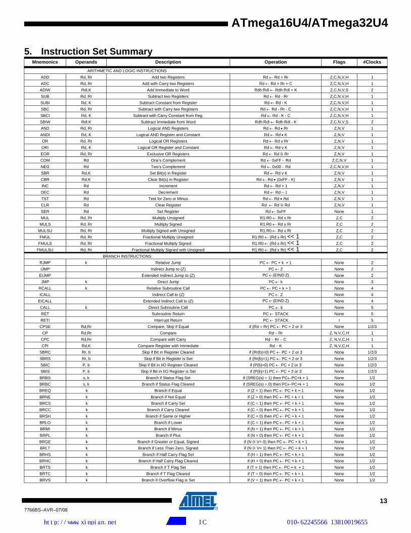
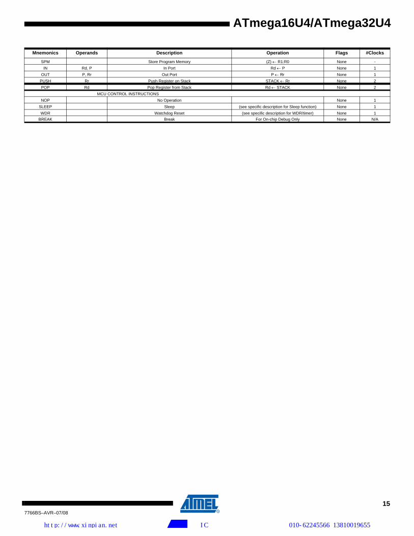
5. Instruction Set SummaryMnemonics Operands Description Operation Flags #Clocks
ARITHMETIC AND LOGIC INSTRUCTIONSADD Rd, Rr Add two Registers Rd ← Rd + Rr Z,C,N,V,H 1ADC Rd, Rr Add with Carry two Registers Rd ← Rd + Rr + C Z,C,N,V,H 1ADIW Rdl,K Add Immediate to Word Rdh:Rdl ← Rdh:Rdl + K Z,C,N,V,S 2SUB Rd, Rr Subtract two Registers Rd ← Rd - Rr Z,C,N,V,H 1SUBI Rd, K Subtract Constant from Register Rd ← Rd - K Z,C,N,V,H 1SBC Rd, Rr Subtract with Carry two Registers Rd ← Rd - Rr - C Z,C,N,V,H 1SBCI Rd, K Subtract with Carry Constant from Reg. Rd ← Rd - K - C Z,C,N,V,H 1SBIW Rdl,K Subtract Immediate from Word Rdh:Rdl ← Rdh:Rdl - K Z,C,N,V,S 2AND Rd, Rr Logical AND Registers Rd ← Rd • Rr Z,N,V 1ANDI Rd, K Logical AND Register and Constant Rd ← Rd • K Z,N,V 1OR Rd, Rr Logical OR Registers Rd ← Rd v Rr Z,N,V 1ORI Rd, K Logical OR Register and Constant Rd ← Rd v K Z,N,V 1EOR Rd, Rr Exclusive OR Registers Rd ← Rd ⊕ Rr Z,N,V 1COM Rd One’s Complement Rd ← 0xFF − Rd Z,C,N,V 1NEG Rd Two’s Complement Rd ← 0x00 − Rd Z,C,N,V,H 1SBR Rd,K Set Bit(s) in Register Rd ← Rd v K Z,N,V 1CBR Rd,K Clear Bit(s) in Register Rd ← Rd • (0xFF - K) Z,N,V 1INC Rd Increment Rd ← Rd + 1 Z,N,V 1DEC Rd Decrement Rd ← Rd − 1 Z,N,V 1TST Rd Test for Zero or Minus Rd ← Rd • Rd Z,N,V 1CLR Rd Clear Register Rd ← Rd ⊕ Rd Z,N,V 1SER Rd Set Register Rd ← 0xFF None 1MUL Rd, Rr Multiply Unsigned R1:R0 ← Rd x Rr Z,C 2
MULS Rd, Rr Multiply Signed R1:R0 ← Rd x Rr Z,C 2MULSU Rd, Rr Multiply Signed with Unsigned R1:R0 ← Rd x Rr Z,C 2FMUL Rd, Rr Fractional Multiply Unsigned R1:R0 ← (Rd x Rr) << 1 Z,C 2
FMULS Rd, Rr Fractional Multiply Signed R1:R0 ← (Rd x Rr) << 1 Z,C 2FMULSU Rd, Rr Fractional Multiply Signed with Unsigned R1:R0 ← (Rd x Rr) << 1 Z,C 2
BRANCH INSTRUCTIONSRJMP k Relative Jump PC ← PC + k + 1 None 2IJMP Indirect Jump to (Z) PC ← Z None 2
EIJMP Extended Indirect Jump to (Z) PC ←(EIND:Z) None 2JMP k Direct Jump PC ← k None 3
RCALL k Relative Subroutine Call PC ← PC + k + 1 None 4ICALL Indirect Call to (Z) PC ← Z None 4
EICALL Extended Indirect Call to (Z) PC ←(EIND:Z) None 4CALL k Direct Subroutine Call PC ← k None 5RET Subroutine Return PC ← STACK None 5RETI Interrupt Return PC ← STACK I 5CPSE Rd,Rr Compare, Skip if Equal if (Rd = Rr) PC ← PC + 2 or 3 None 1/2/3
CP Rd,Rr Compare Rd − Rr Z, N,V,C,H 1 CPC Rd,Rr Compare with Carry Rd − Rr − C Z, N,V,C,H 1CPI Rd,K Compare Register with Immediate Rd − K Z, N,V,C,H 1
SBRC Rr, b Skip if Bit in Register Cleared if (Rr(b)=0) PC ← PC + 2 or 3 None 1/2/3SBRS Rr, b Skip if Bit in Register is Set if (Rr(b)=1) PC ← PC + 2 or 3 None 1/2/3SBIC P, b Skip if Bit in I/O Register Cleared if (P(b)=0) PC ← PC + 2 or 3 None 1/2/3SBIS P, b Skip if Bit in I/O Register is Set if (P(b)=1) PC ← PC + 2 or 3 None 1/2/3BRBS s, k Branch if Status Flag Set if (SREG(s) = 1) then PC←PC+k + 1 None 1/2BRBC s, k Branch if Status Flag Cleared if (SREG(s) = 0) then PC←PC+k + 1 None 1/2BREQ k Branch if Equal if (Z = 1) then PC ← PC + k + 1 None 1/2BRNE k Branch if Not Equal if (Z = 0) then PC ← PC + k + 1 None 1/2BRCS k Branch if Carry Set if (C = 1) then PC ← PC + k + 1 None 1/2BRCC k Branch if Carry Cleared if (C = 0) then PC ← PC + k + 1 None 1/2BRSH k Branch if Same or Higher if (C = 0) then PC ← PC + k + 1 None 1/2BRLO k Branch if Lower if (C = 1) then PC ← PC + k + 1 None 1/2BRMI k Branch if Minus if (N = 1) then PC ← PC + k + 1 None 1/2BRPL k Branch if Plus if (N = 0) then PC ← PC + k + 1 None 1/2BRGE k Branch if Greater or Equal, Signed if (N ⊕ V= 0) then PC ← PC + k + 1 None 1/2BRLT k Branch if Less Than Zero, Signed if (N ⊕ V= 1) then PC ← PC + k + 1 None 1/2BRHS k Branch if Half Carry Flag Set if (H = 1) then PC ← PC + k + 1 None 1/2BRHC k Branch if Half Carry Flag Cleared if (H = 0) then PC ← PC + k + 1 None 1/2BRTS k Branch if T Flag Set if (T = 1) then PC ← PC + k + 1 None 1/2BRTC k Branch if T Flag Cleared if (T = 0) then PC ← PC + k + 1 None 1/2BRVS k Branch if Overflow Flag is Set if (V = 1) then PC ← PC + k + 1 None 1/2
137766BS–AVR–07/08
http://www.xinpian.net 提供单片机解密、IC解密、芯片解密业务 010-62245566 13810019655
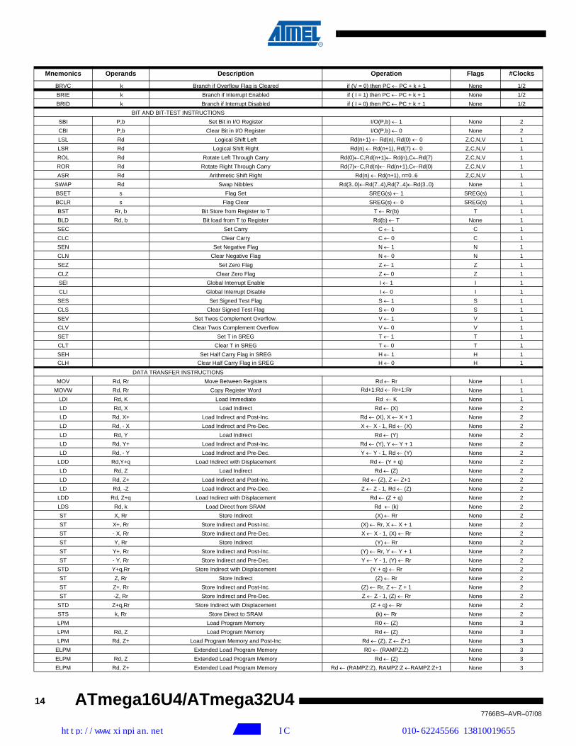
BRVC k Branch if Overflow Flag is Cleared if (V = 0) then PC ← PC + k + 1 None 1/2BRIE k Branch if Interrupt Enabled if ( I = 1) then PC ← PC + k + 1 None 1/2BRID k Branch if Interrupt Disabled if ( I = 0) then PC ← PC + k + 1 None 1/2
BIT AND BIT-TEST INSTRUCTIONSSBI P,b Set Bit in I/O Register I/O(P,b) ← 1 None 2CBI P,b Clear Bit in I/O Register I/O(P,b) ← 0 None 2LSL Rd Logical Shift Left Rd(n+1) ← Rd(n), Rd(0) ← 0 Z,C,N,V 1LSR Rd Logical Shift Right Rd(n) ← Rd(n+1), Rd(7) ← 0 Z,C,N,V 1ROL Rd Rotate Left Through Carry Rd(0)←C,Rd(n+1)← Rd(n),C←Rd(7) Z,C,N,V 1ROR Rd Rotate Right Through Carry Rd(7)←C,Rd(n)← Rd(n+1),C←Rd(0) Z,C,N,V 1ASR Rd Arithmetic Shift Right Rd(n) ← Rd(n+1), n=0..6 Z,C,N,V 1
SWAP Rd Swap Nibbles Rd(3..0)←Rd(7..4),Rd(7..4)←Rd(3..0) None 1BSET s Flag Set SREG(s) ← 1 SREG(s) 1BCLR s Flag Clear SREG(s) ← 0 SREG(s) 1BST Rr, b Bit Store from Register to T T ← Rr(b) T 1BLD Rd, b Bit load from T to Register Rd(b) ← T None 1SEC Set Carry C ← 1 C 1CLC Clear Carry C ← 0 C 1SEN Set Negative Flag N ← 1 N 1CLN Clear Negative Flag N ← 0 N 1SEZ Set Zero Flag Z ← 1 Z 1CLZ Clear Zero Flag Z ← 0 Z 1SEI Global Interrupt Enable I ← 1 I 1CLI Global Interrupt Disable I ← 0 I 1SES Set Signed Test Flag S ← 1 S 1CLS Clear Signed Test Flag S ← 0 S 1SEV Set Twos Complement Overflow. V ← 1 V 1CLV Clear Twos Complement Overflow V ← 0 V 1SET Set T in SREG T ← 1 T 1CLT Clear T in SREG T ← 0 T 1SEH Set Half Carry Flag in SREG H ← 1 H 1CLH Clear Half Carry Flag in SREG H ← 0 H 1
DATA TRANSFER INSTRUCTIONSMOV Rd, Rr Move Between Registers Rd ← Rr None 1
MOVW Rd, Rr Copy Register Word Rd+1:Rd ← Rr+1:Rr None 1LDI Rd, K Load Immediate Rd ← K None 1LD Rd, X Load Indirect Rd ← (X) None 2LD Rd, X+ Load Indirect and Post-Inc. Rd ← (X), X ← X + 1 None 2LD Rd, - X Load Indirect and Pre-Dec. X ← X - 1, Rd ← (X) None 2LD Rd, Y Load Indirect Rd ← (Y) None 2LD Rd, Y+ Load Indirect and Post-Inc. Rd ← (Y), Y ← Y + 1 None 2LD Rd, - Y Load Indirect and Pre-Dec. Y ← Y - 1, Rd ← (Y) None 2
LDD Rd,Y+q Load Indirect with Displacement Rd ← (Y + q) None 2LD Rd, Z Load Indirect Rd ← (Z) None 2LD Rd, Z+ Load Indirect and Post-Inc. Rd ← (Z), Z ← Z+1 None 2LD Rd, -Z Load Indirect and Pre-Dec. Z ← Z - 1, Rd ← (Z) None 2
LDD Rd, Z+q Load Indirect with Displacement Rd ← (Z + q) None 2LDS Rd, k Load Direct from SRAM Rd ← (k) None 2ST X, Rr Store Indirect (X) ← Rr None 2ST X+, Rr Store Indirect and Post-Inc. (X) ← Rr, X ← X + 1 None 2ST - X, Rr Store Indirect and Pre-Dec. X ← X - 1, (X) ← Rr None 2ST Y, Rr Store Indirect (Y) ← Rr None 2ST Y+, Rr Store Indirect and Post-Inc. (Y) ← Rr, Y ← Y + 1 None 2ST - Y, Rr Store Indirect and Pre-Dec. Y ← Y - 1, (Y) ← Rr None 2
STD Y+q,Rr Store Indirect with Displacement (Y + q) ← Rr None 2ST Z, Rr Store Indirect (Z) ← Rr None 2ST Z+, Rr Store Indirect and Post-Inc. (Z) ← Rr, Z ← Z + 1 None 2ST -Z, Rr Store Indirect and Pre-Dec. Z ← Z - 1, (Z) ← Rr None 2
STD Z+q,Rr Store Indirect with Displacement (Z + q) ← Rr None 2STS k, Rr Store Direct to SRAM (k) ← Rr None 2LPM Load Program Memory R0 ← (Z) None 3LPM Rd, Z Load Program Memory Rd ← (Z) None 3LPM Rd, Z+ Load Program Memory and Post-Inc Rd ← (Z), Z ← Z+1 None 3
ELPM Extended Load Program Memory R0 ← (RAMPZ:Z) None 3ELPM Rd, Z Extended Load Program Memory Rd ← (Z) None 3ELPM Rd, Z+ Extended Load Program Memory Rd ← (RAMPZ:Z), RAMPZ:Z ←RAMPZ:Z+1 None 3
Mnemonics Operands Description Operation Flags #Clocks
147766BS–AVR–07/08
ATmega16U4/ATmega32U4http://www.xinpian.net 提供单片机解密、IC解密、芯片解密业务 010-62245566 13810019655
ATmega16U4/ATmega32U4
SPM Store Program Memory (Z) ← R1:R0 None -IN Rd, P In Port Rd ← P None 1
OUT P, Rr Out Port P ← Rr None 1PUSH Rr Push Register on Stack STACK ← Rr None 2POP Rd Pop Register from Stack Rd ← STACK None 2
MCU CONTROL INSTRUCTIONSNOP No Operation None 1
SLEEP Sleep (see specific description for Sleep function) None 1WDR Watchdog Reset (see specific description for WDR/timer) None 1
BREAK Break For On-chip Debug Only None N/A
Mnemonics Operands Description Operation Flags #Clocks
7766BS–AVR–07/08
http://www.xinpi
15
an.net 提供单片机解密、IC解密、芯片解密业务 010-62245566 13810019655

16 ATmegahttp://www.xinpi
7766BS–AVR–07/08
16U4/ATmega32U4an.net 提供单片机解密、IC解密、芯片解密业务 010-62245566 13810019655
ATmega16U4/ATmega32U4
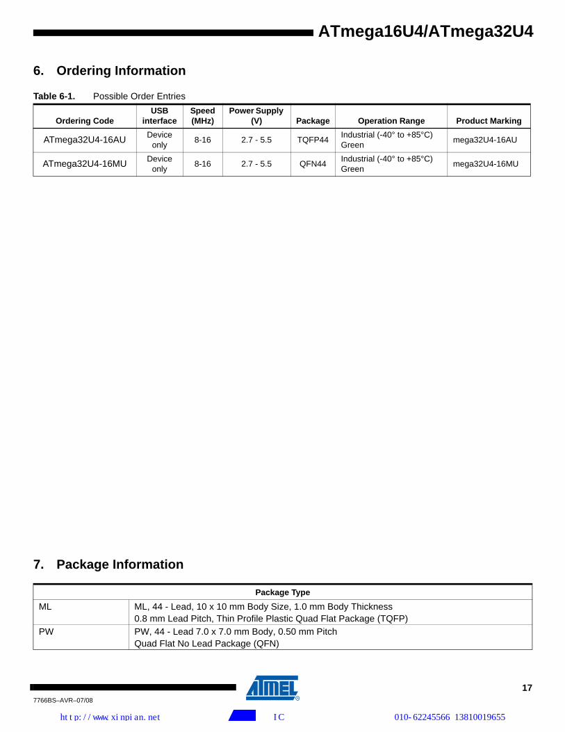
6. Ordering Information
7766BS–AVR–07/08
http://www.xinpi
Table 6-1. Possible Order Entries
Ordering Code USB
interfaceSpeed (MHz)
Power Supply (V) Package Operation Range Product Marking
ATmega32U4-16AU Device only 8-16 2.7 - 5.5 TQFP44 Industrial (-40° to +85°C)
Green mega32U4-16AU
ATmega32U4-16MU Device only 8-16 2.7 - 5.5 QFN44 Industrial (-40° to +85°C)
Green mega32U4-16MU
7. Package Information
Package Type
ML ML, 44 - Lead, 10 x 10 mm Body Size, 1.0 mm Body Thickness0.8 mm Lead Pitch, Thin Profile Plastic Quad Flat Package (TQFP)
PW PW, 44 - Lead 7.0 x 7.0 mm Body, 0.50 mm PitchQuad Flat No Lead Package (QFN)
17
an.net 提供单片机解密、IC解密、芯片解密业务 010-62245566 13810019655
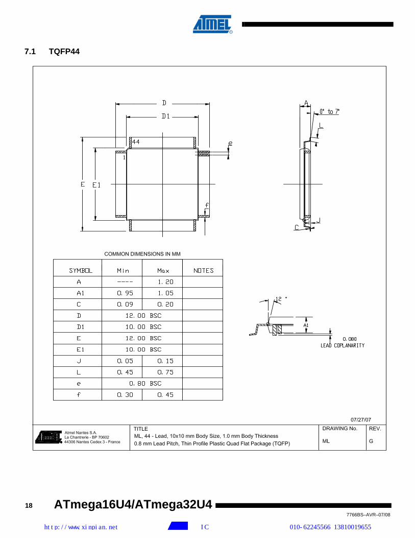
7.1 TQFP44
18 ATmegahttp://www.xinpi
7766BS–AVR–07/08
16U4/ATmega32U4an.net 提供单片机解密、IC解密、芯片解密业务 010-62245566 13810019655

7766BS–AVR–07/08
ATmega16U4/ATmega32U4
http://www.xinpi
19
an.net 提供单片机解密、IC解密、芯片解密业务 010-62245566 13810019655
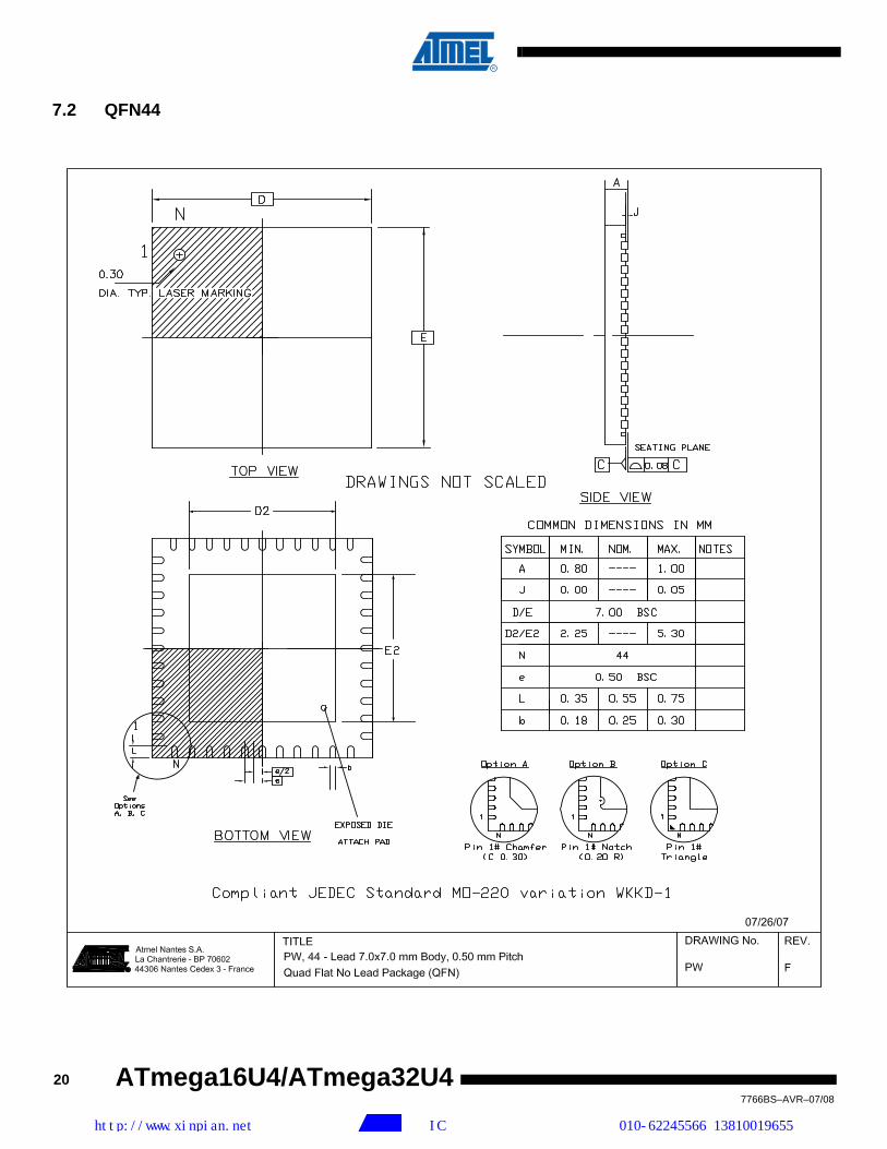
7.2 QFN44
207766BS–AVR–07/08
ATmega16U4/ATmega32U4http://www.xinpian.net 提供单片机解密、IC解密、芯片解密业务 010-62245566 13810019655

ATmega16U4/ATmega32U4
8. Errata
7766BS–AVR–07/08
http://www.xinpi
The revision letter in this section refers to the revision of the ATmega16U4/ATmega32U4device.
8.1 ATmega16U4/ATmega32U4 Rev A
1. Spike on TWI pins when TWI is enabled100 ns negative spike occurs on SDA and SCL pins when TWI is enabled.
Problem Fix/work aroundNo known work around, enable ATmega16U4/ATmega32U4 TWI first versus the othersnodes of the TWI network.
2. High current consumption in sleep modeIf a pending interrupt cannot wake the part up from the selected mode, the current consump-tion will increase during sleep when executing the SLEEP instruction directly after a SEIinstruction.
Problem Fix/work aroundBefore entering sleep, interrupts not used to wake up the part from the sleep mode shouldbe disabled.
3. Extra power comsumptionThe typical power comsumption is increased by about 30µA in power-down mode.
Problem Fix/work aroundNone.
4. Internal RC oscillator start up issue.When the part is configured to start on internal RC, the oscillator may not start properly afterpower-on.
Problem Fix/work aroundDo not configure the part to start with the internal oscillator (default part configuration is tostart with the external crystal oscillator).
5. Internal RC oscillator calibration issue.The default internal RC oscillator frequency may be lower that 8MHz.
Problem Fix/work aroundParts are configured so that the internal RC oscillator frequency is as close as possible tothe 8MHz default target frequency.
21
an.net 提供单片机解密、IC解密、芯片解密业务 010-62245566 13810019655
9. Datasheet Revision History for ATmega16U4/ATmega32U4
22 ATmegahttp://www.xinpi
Please note that the referring page numbers in this section are referred to this document. Thereferring revision in this section are referring to the document revision.
9.1 Revision A.
1. Initial document version.9.2 Revision B.
1. Added ATmega16U4 device.2. Created errata section and added ATmega16U4.3. Update High Speed Timer, asynchronous description Section 15. on page 139.7766BS–AVR–07/08
16U4/ATmega32U4an.net 提供单片机解密、IC解密、芯片解密业务 010-62245566 13810019655

Headquarters
Atmel Corporation2325 Orchard ParkwaySan Jose, CA 95131USATel: 1(408) 441-0311Fax: 1(408) 487-2600
Disclaimer: The information in tintellectual property right is grantTIONS OF SALE LOCATED ON AWARRANTY RELATING TO ITS PPURPOSE, OR NON-INFRINGEMTAL DAMAGES (INCLUDING, WITOF THE USE OR INABILITY TOrepresentations or warranties withand product descriptions at any totherwise, Atmel products are noas components in applications int
© 2008 Atmel Corporation. AAtmel Corporation or its subs
http://www.xinpi
International
Atmel AsiaRoom 1219Chinachem Golden Plaza77 Mody Road TsimshatsuiEast KowloonHong KongTel: (852) 2721-9778Fax: (852) 2722-1369
Atmel EuropeLe Krebs8, Rue Jean-Pierre TimbaudBP 30978054 Saint-Quentin-en-Yvelines CedexFranceTel: (33) 1-30-60-70-00 Fax: (33) 1-30-60-71-11
Atmel Japan9F, Tonetsu Shinkawa Bldg.1-24-8 ShinkawaChuo-ku, Tokyo 104-0033JapanTel: (81) 3-3523-3551Fax: (81) 3-3523-7581
Product Contact
Web Sitewww.atmel.com
Technical [email protected]
Sales Contactwww.atmel.com/contacts
Literature Requestswww.atmel.com/literature
his document is provided in connection with Atmel products. No license, express or implied, by estoppel or otherwise, to anyed by this document or in connection with the sale of Atmel products. EXCEPT AS SET FORTH IN ATMEL’S TERMS AND CONDI-TMEL’S WEB SITE, ATMEL ASSUMES NO LIABILITY WHATSOEVER AND DISCLAIMS ANY EXPRESS, IMPLIED OR STATUTORYRODUCTS INCLUDING, BUT NOT LIMITED TO, THE IMPLIED WARRANTY OF MERCHANTABILITY, FITNESS FOR A PARTICULAR
ENT. IN NO EVENT SHALL ATMEL BE LIABLE FOR ANY DIRECT, INDIRECT, CONSEQUENTIAL, PUNITIVE, SPECIAL OR INCIDEN-HOUT LIMITATION, DAMAGES FOR LOSS OF PROFITS, BUSINESS INTERRUPTION, OR LOSS OF INFORMATION) ARISING OUT USE THIS DOCUMENT, EVEN IF ATMEL HAS BEEN ADVISED OF THE POSSIBILITY OF SUCH DAMAGES. Atmel makes no respect to the accuracy or completeness of the contents of this document and reserves the right to make changes to specifications
ime without notice. Atmel does not make any commitment to update the information contained herein. Unless specifically providedt suitable for, and shall not be used in, automotive applications. Atmel’s products are not intended, authorized, or warranted for useended to support or sustain life.
ll rights reserved. Atmel®, logo and combinations thereof, and others are registered trademarks or trademarks ofidiaries. Other terms and product names may be trademarks of others.
7766BS–AVR–07/08
an.net 提供单片机解密、IC解密、芯片解密业务 010-62245566 13810019655