7I92 ETHERNET ANYTHING I/O MANUAL
41
7I92 ETHERNET ANYTHING I/O MANUAL Version 1.7
Transcript of 7I92 ETHERNET ANYTHING I/O MANUAL

7I92 ETHERNET ANYTHING I/O MANUAL
Version 1.7

This page intentionally not blank
iii
Table of Contents
GENERAL . . . . . . . . . . . . . . . . . . . . . . . . . . . . . . . . . . . . . . . . . . . . . . . . . . . . . . . . . . 1
DESCRIPTION . . . . . . . . . . . . . . . . . . . . . . . . . . . . . . . . . . . . . . . . . . . . . . . . . 1
HARDWARE CONFIGURATION . . . . . . . . . . . . . . . . . . . . . . . . . . . . . . . . . . . . . . . . 2
GENERAL . . . . . . . . . . . . . . . . . . . . . . . . . . . . . . . . . . . . . . . . . . . . . . . . . . . . 2BREAKOUT POWER OPTION . . . . . . . . . . . . . . . . . . . . . . . . . . . . . . . . . . . . . 25V I/O TOLERANCE . . . . . . . . . . . . . . . . . . . . . . . . . . . . . . . . . . . . . . . . . . . . 2PRECONFIG PULL-UP ENABLE . . . . . . . . . . . . . . . . . . . . . . . . . . . . . . . . . . . 3IP ADDRESS SELECTION . . . . . . . . . . . . . . . . . . . . . . . . . . . . . . . . . . . . . . . . 3
CONNECTORS . . . . . . . . . . . . . . . . . . . . . . . . . . . . . . . . . . . . . . . . . . . . . . . . . . . . . . 4
CONNECTOR LOCATIONS AND DEFAULT JUMPER POSITIONS . . . . . . . . 47I92 I/O CONNECTOR PIN-OUT . . . . . . . . . . . . . . . . . . . . . . . . . . . . . . . . . . . 5POWER CONNECTOR PIN-OUT . . . . . . . . . . . . . . . . . . . . . . . . . . . . . . . . . . 7JTAG CONNECTOR PIN-OUT . . . . . . . . . . . . . . . . . . . . . . . . . . . . . . . . . . . . . 7
OPERATION . . . . . . . . . . . . . . . . . . . . . . . . . . . . . . . . . . . . . . . . . . . . . . . . . . . . . . . . 8
FPGA . . . . . . . . . . . . . . . . . . . . . . . . . . . . . . . . . . . . . . . . . . . . . . . . . . . . . . . . 8FPGA PINOUT . . . . . . . . . . . . . . . . . . . . . . . . . . . . . . . . . . . . . . . . . . . . . . . . . 8IP ADDRESS SELECTION . . . . . . . . . . . . . . . . . . . . . . . . . . . . . . . . . . . . . . . . 8HOST COMMUNICATION . . . . . . . . . . . . . . . . . . . . . . . . . . . . . . . . . . . . . . . . 8UDP . . . . . . . . . . . . . . . . . . . . . . . . . . . . . . . . . . . . . . . . . . . . . . . . . . . . . . . . . 8LBP16 . . . . . . . . . . . . . . . . . . . . . . . . . . . . . . . . . . . . . . . . . . . . . . . . . . . . . . . 8WINDOWS ARP ISSUES . . . . . . . . . . . . . . . . . . . . . . . . . . . . . . . . . . . . . . . . . 8CONFIGURATION . . . . . . . . . . . . . . . . . . . . . . . . . . . . . . . . . . . . . . . . . . . . . . 9FALLBACK . . . . . . . . . . . . . . . . . . . . . . . . . . . . . . . . . . . . . . . . . . . . . . . . . . . . 9DUAL EEPROMS . . . . . . . . . . . . . . . . . . . . . . . . . . . . . . . . . . . . . . . . . . . . . . . 9EEPROM LAYOUT . . . . . . . . . . . . . . . . . . . . . . . . . . . . . . . . . . . . . . . . . . . . . 10BITFILE FORMAT . . . . . . . . . . . . . . . . . . . . . . . . . . . . . . . . . . . . . . . . . . . . . 12

iv
Table of Contents
OPERATION . . . . . . . . . . . . . . . . . . . . . . . . . . . . . . . . . . . . . . . . . . . . . . . . . . . . . . . 8
MESAFLASH . . . . . . . . . . . . . . . . . . . . . . . . . . . . . . . . . . . . . . . . . . . . . . . . . 12SETTING EEPROM IP ADDRESS . . . . . . . . . . . . . . . . . . . . . . . . . . . 12
FREE EEPROM SPACE . . . . . . . . . . . . . . . . . . . . . . . . . . . . . . . . . . . . . . . . 13FALLBACK INDICATION . . . . . . . . . . . . . . . . . . . . . . . . . . . . . . . . . . . . . . . . 13FAILURE TO CONFIGURE . . . . . . . . . . . . . . . . . . . . . . . . . . . . . . . . . . . . . . 13CLOCK SIGNALS . . . . . . . . . . . . . . . . . . . . . . . . . . . . . . . . . . . . . . . . . . . . . . 13LEDS . . . . . . . . . . . . . . . . . . . . . . . . . . . . . . . . . . . . . . . . . . . . . . . . . . . . . . . 14PULLUP RESISTORS . . . . . . . . . . . . . . . . . . . . . . . . . . . . . . . . . . . . . . . . . . 14I/O LEVELS . . . . . . . . . . . . . . . . . . . . . . . . . . . . . . . . . . . . . . . . . . . . . . . . . . 14STARTUP I/O VOLTAGE . . . . . . . . . . . . . . . . . . . . . . . . . . . . . . . . . . . . . . . . 14INTERFACE CABLES . . . . . . . . . . . . . . . . . . . . . . . . . . . . . . . . . . . . . . . . . . 15

v
Table of Contents
SUPPLIED CONFIGURATIONS . . . . . . . . . . . . . . . . . . . . . . . . . . . . . . . . . . . . . . . . 16
HOSTMOT2 . . . . . . . . . . . . . . . . . . . . . . . . . . . . . . . . . . . . . . . . . . . . . . . . . . 167I76X1D . . . . . . . . . . . . . . . . . . . . . . . . . . . . . . . . . . . . . . . . . . . . . . . . . . . . . 167I76_7I74D . . . . . . . . . . . . . . . . . . . . . . . . . . . . . . . . . . . . . . . . . . . . . . . . . . . 16G540X2D . . . . . . . . . . . . . . . . . . . . . . . . . . . . . . . . . . . . . . . . . . . . . . . . . . . . 167I77X2D . . . . . . . . . . . . . . . . . . . . . . . . . . . . . . . . . . . . . . . . . . . . . . . . . . . . . 167I77_7I76D . . . . . . . . . . . . . . . . . . . . . . . . . . . . . . . . . . . . . . . . . . . . . . . . . . . 167I77_7I74D . . . . . . . . . . . . . . . . . . . . . . . . . . . . . . . . . . . . . . . . . . . . . . . . . . . 177I74X2D . . . . . . . . . . . . . . . . . . . . . . . . . . . . . . . . . . . . . . . . . . . . . . . . . . . . . 177I78X2D . . . . . . . . . . . . . . . . . . . . . . . . . . . . . . . . . . . . . . . . . . . . . . . . . . . . . 17PROB_RFX2D . . . . . . . . . . . . . . . . . . . . . . . . . . . . . . . . . . . . . . . . . . . . . . . . 17PIN FILES . . . . . . . . . . . . . . . . . . . . . . . . . . . . . . . . . . . . . . . . . . . . . . . . . . . 17
REFERENCE INFORMATION . . . . . . . . . . . . . . . . . . . . . . . . . . . . . . . . . . . . . . . . . 18LBP16
LBP16 COMMANDS . . . . . . . . . . . . . . . . . . . . . . . . . . . . . . . . . . . . . . 18INFO AREA . . . . . . . . . . . . . . . . . . . . . . . . . . . . . . . . . . . . . . . . . . . . . 19INFO AREA MEMSIZES FORMAT . . . . . . . . . . . . . . . . . . . . . . . . . . . 19INFO AREA MEMRANGES FORMAT . . . . . . . . . . . . . . . . . . . . . . . . . 20INFO AREA ACCESS . . . . . . . . . . . . . . . . . . . . . . . . . . . . . . . . . . . . . 217I92 SUPPORTED MEMORY SPACES . . . . . . . . . . . . . . . . . . . . . . . . 22SPACE0: HOSTMOT2 REGISTERS . . . . . . . . . . . . . . . . . . . . . . . . . . 22SPACE1: ETHERNET CHIP ACCESS . . . . . . . . . . . . . . . . . . . . . . . . . 24SPACE2: ETHERNET EEPROM CHIP ACCESS . . . . . . . . . . . . . . . . 24ETHERNET EEPROM LAYOUT . . . . . . . . . . . . . . . . . . . . . . . . . . . . . 25SPACE3: FPGA FLASH EEPROM CHIP ACCESS . . . . . . . . . . . . . . . 27FLASH MEMORY REGISTERS . . . . . . . . . . . . . . . . . . . . . . . . . . . . . . 27SPACE4: LBP TIMER/UTIL REGISTERS . . . . . . . . . . . . . . . . . . . . . . 30SPACE6: LBP STATUS/CONTROL REGISTERS . . . . . . . . . . . . . . . . 31MEMORY SPACE 6 LAYOUT . . . . . . . . . . . . . . . . . . . . . . . . . . . . . . . 31ERROR REGISTER FORMAT . . . . . . . . . . . . . . . . . . . . . . . . . . . . . . . 32SPACE7: LBP READ ONLY INFORMATION . . . . . . . . . . . . . . . . . . . . 33MEMORY SPACE 7 LAYOUT . . . . . . . . . . . . . . . . . . . . . . . . . . . . . . . 33ELBPCOM . . . . . . . . . . . . . . . . . . . . . . . . . . . . . . . . . . . . . . . . . . . . . . 34
SPECIFICATIONS . . . . . . . . . . . . . . . . . . . . . . . . . . . . . . . . . . . . . . . . . . . . . 35CARD DRAWING . . . . . . . . . . . . . . . . . . . . . . . . . . . . . . . . . . . . . . . . . . . . . . 36
7I92 1
GENERAL
DESCRIPTION
The MESA 7I92 is a low cost, general purpose, FPGA based programmable I/O cardwith 100 BaseT Ethernet host connection. The 7I92 that uses standard parallel port pinoutsand connectors for compatibility with most parallel port interfaced motion control / CNCbreakout cards/ multi axis step motor drives, allowing a motion control performance boostwhile retaining a reliable real time Ethernet interface. Unlike the parallel port that the 7I92replaces, each I/O bit has individually programmable direction and function.
The 7I92 has a simplified UDP host data transfer systems that allows operation inreal time and compatibility with standard networks. The 7I92 provides 34 I/O bits (17 perconnector) All I/O bits are 5V tolerant and have pullup resistors. A power source optionallows the 7I92 to supply 5V power to breakout boards if desired. This 5V power is protectedby a PTC.
Firmware modules are provided for hardware step generation, quadrature encodercounting, PWM generation, digital I/O, Smart Serial remote I/O, BISS, SSI, SPI, UARTinterfaces and more. Configurations are available that are compatible with commonbreakout cards and multi axis step motor drives like the Gecko G540 andLeadshineMX3660/4660. All motion control firmware is open source and easily modified tosupport new functions or different mixes of functions.
In addition to standard parallel port breakouts, There are currently six 7I92compatible breakout cards available from Mesa, the 7I74 through 7I78 and 7I85. The 7I76is a step/dir oriented breakout with 5 axis of buffered step/dir outputs, one spindle encoderinput, one isolated 0-10V analog spindle speed plus isolated direction and enable outputs,one RS-422 expansion port, 32 isolated 5-32V inputs and 16 isolated 5-32V 300 mAoutputs. The 7I77 is a analog servo interface with 6 encoder inputs, 6 analog +-10V outputs,one RS-422 expansion port, 32 isolated 5-32V inputs, and 16 isolated 5-32V 300 mAoutputs. The 7I92 supports two breakout cards so for example a 10 Axis step/dirconfiguration or 12 axis analog servo configuration is possible with a single 7I92 and twoMesa breakout cards.

7I92 2
HARDWARE CONFIGURATION
GENERAL
Hardware setup jumper positions assume that the 7I92 card is oriented in an uprightposition, that is, with the Ethernet connector towards the left and the I/O connectorstowards the right.
CONNECTOR 5V POWER
The 7I92 has the option to supply 5V power from the to the breakout board. Thisoption is used by all Mesa breakout boards to simplify wiring. The option uses 4 parallelcable signals that are normally used as grounds for supplying 5V to the remote breakoutboard (DB25 pins 22,23,24 and 25). These pins are AC bypassed on both the 7I92 andMesa breakout cards so do not compromise AC signal integrity. The 5V power option isindividually selectable for each of the four I/O connectors. The breakout 5V power isprotected by per connector PTC devices so will not cause damage to the 7I92 or systemif accidentally shorted. This option should only be enabled for Mesa breakout boards orboards specifically wired to accept 5V power on DB25 pins 22 through 25. When the optionis disabled DB25 pins 22 through 25 are grounded. Jumper W3 sets the power option onheader P1, and W4 sets the power option on DB25 connector P2.
JUMPER POS FUNCTION
W3,W4 UP BREAKOUT POWER ENABLED
W3,W4 DOWN BREAKOUT POWER DISABLED (DEFAULT)
5V I/O TOLERANCE
The FPGA used on the 7I92 has a 4V absolute maximum input voltagespecification. To allow interfacing with 5V inputs, the 7I92 has bus switches on all I/O pins.The bus switches work by turning off when the input voltage exceeds a preset threshold.The 5V I/O tolerance option is the default and should normally be left enabled.
For high speed applications where only 3.3V maximum signals are present andovershoot clamping is desired, the 5V I/O tolerance option can be disabled. W1 controlsthe 5V I/O tolerance option. When W1 is on the default UP position, 5V tolerance modeis enabled. When W1 is in the DOWN position, 5V tolerance mode is disabled. Note thatW4 controls 5V tolerance on both I/O connectors.
PULLUP VOLTAGE
Jumper W1 also selects the I/O connector pull-up resistor voltage, When W1 is inthe UP position the 4.7K I/O pullup resistor common is connected to 5V, When W1 is inthe down position, The 4.7K I/O pullup resistor common is connected to 3.3V.

7I92 3
HARDWARE CONFIGURATION
IP ADDRESS SELECTION
The 7I92 has three options for selecting its IP address. These options are selectedby Jumpers W5 and W6.
W5 W6 IP ADDRESS
DOWN DOWN FIXED 192.168.1.121 (DEFAULT)
DOWN UP FIXED FROM EEPROM
UP DOWN BOOTP
UP UP INVALID
Note: that the initial EEPROM IP address is set to 10.10.10.10 at Mesa, but can bechanged to any address with the mesaflash utility.
7I92 4
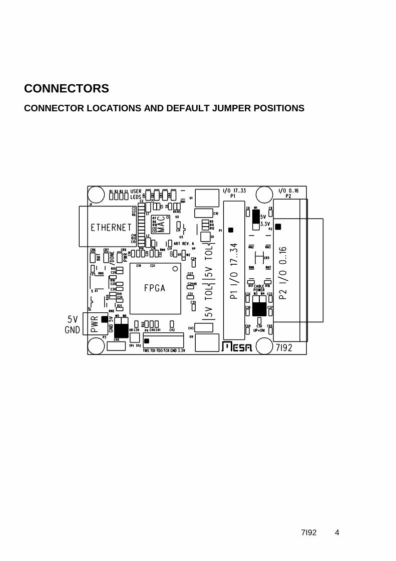
CONNECTORS
CONNECTOR LOCATIONS AND DEFAULT JUMPER POSITIONS
7I92 5
CONNECTORS
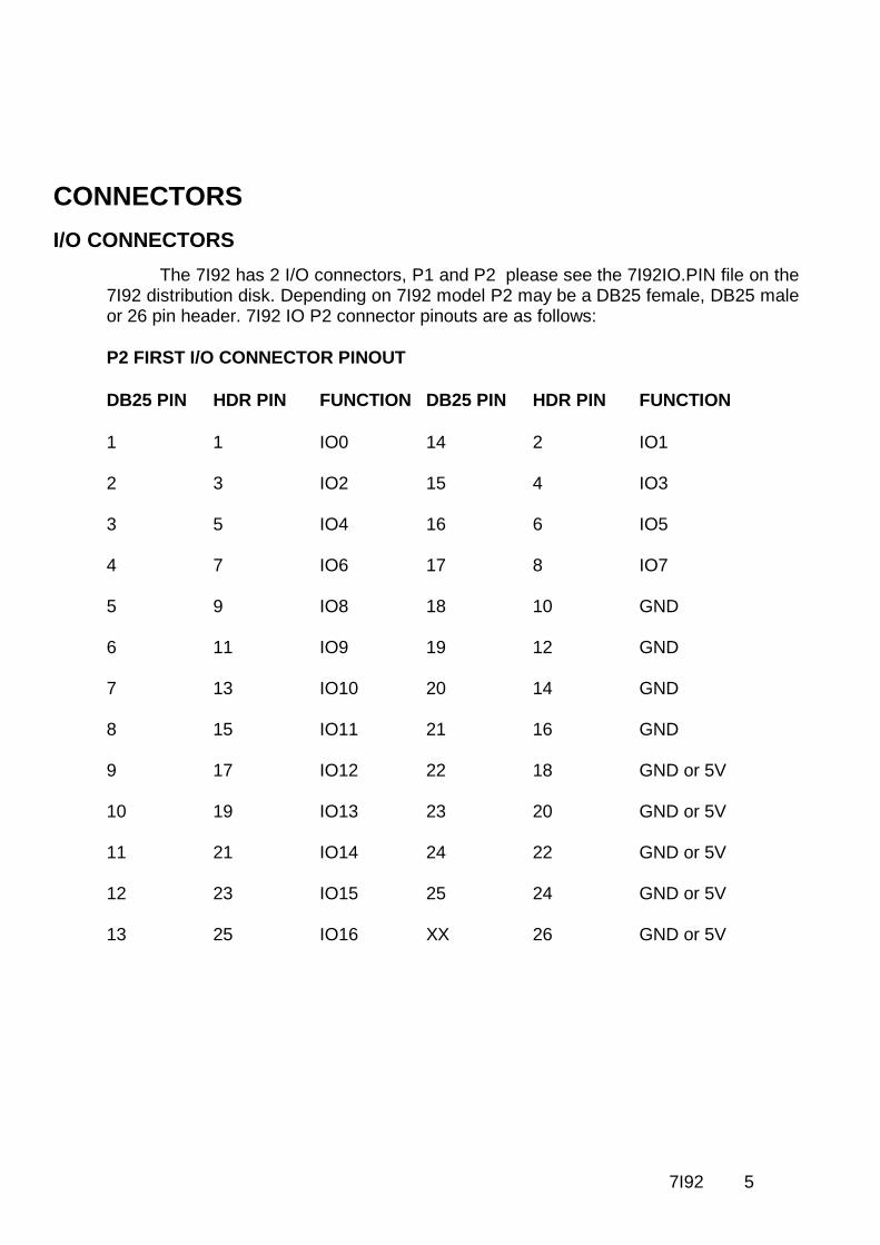
I/O CONNECTORS
The 7I92 has 2 I/O connectors, P1 and P2 please see the 7I92IO.PIN file on the7I92 distribution disk. Depending on 7I92 model P2 may be a DB25 female, DB25 maleor 26 pin header. 7I92 IO P2 connector pinouts are as follows:
P2 FIRST I/O CONNECTOR PINOUT
DB25 PIN HDR PIN FUNCTION DB25 PIN HDR PIN FUNCTION
1 1 IO0 14 2 IO1
2 3 IO2 15 4 IO3
3 5 IO4 16 6 IO5
4 7 IO6 17 8 IO7
5 9 IO8 18 10 GND
6 11 IO9 19 12 GND
7 13 IO10 20 14 GND
8 15 IO11 21 16 GND
9 17 IO12 22 18 GND or 5V
10 19 IO13 23 20 GND or 5V
11 21 IO14 24 22 GND or 5V
12 23 IO15 25 24 GND or 5V
13 25 IO16 XX 26 GND or 5V
7I92 6
CONNECTORS
I/O CONNECTORS
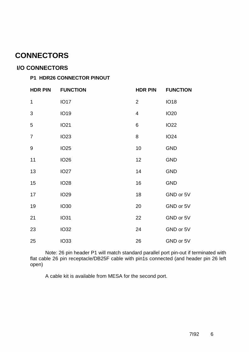
P1 HDR26 CONNECTOR PINOUT
HDR PIN FUNCTION HDR PIN FUNCTION
1 IO17 2 IO18
3 IO19 4 IO20
5 IO21 6 IO22
7 IO23 8 IO24
9 IO25 10 GND
11 IO26 12 GND
13 IO27 14 GND
15 IO28 16 GND
17 IO29 18 GND or 5V
19 IO30 20 GND or 5V
21 IO31 22 GND or 5V
23 IO32 24 GND or 5V
25 IO33 26 GND or 5V
Note: 26 pin header P1 will match standard parallel port pin-out if terminated withflat cable 26 pin receptacle/DB25F cable with pin1s connected (and header pin 26 leftopen)
A cable kit is available from MESA for the second port.

7I92 7
CONNECTORS
POWER CONNECTOR PINOUT
P3 is the 7I92s power connector. P3 is a 3.5MM plug-in screw terminal block. P3pinout is as follows:
PIN FUNCTION
1 +5V TOP, SQUARE PAD
2 GND BOTTOM, ROUND PAD
JTAG CONNECTOR PINOUT
P4 is a JTAG programming connector. This is normally used only for debugging orif both EEPROM configurations have been corrupted. In case of corrupted EEPROMcontents the EEPROM can be re-programmed using Xilinx’s Impact tool.
P4 JTAG CONNECTOR PINOUT
PIN FUNCTION
1 TMS
2 TDI
3 TDO
4 TCK
5 GND
6 +3.3V
7I92 8
OPERATION
FPGA
The 7I92 use a Xilinx Spartan6 XC6SLX9-TQ144 Spartan6 FPGA.
IP ADDRESS SELECTION
Initial communication with the 7I92 requires knowing its IP address. The 7I92 has3 IP address options: Default, EEPROM, and Bootp, selected by jumpers W5 and W6.Default IP address is always 192.168.1.121. The EEPROM IP address is set by writingEthernet EEPROM locations 0x20 and 0X22. BootP allows the 7I92 address to be set bya DHCP/ BootP server. If BootP is chosen, the 7I92 will retry BootP requests at a ~1 Hzrate if the BootP server does not respond.
HOST COMMUNICATION
The 7I92 standard firmware is designed for low overhead real time communicationwith a host controller so implements a very simple set of IPV4 operations. Theseoperations include ARP reply, ICMP echo reply, and UDP packet receive/send for hostdata communications. UDP is used so that the 7I92 can be used on a standard networkwith standard tools for non-real time applications. No fragmentation is allowed somaximum packet size is 1500 bytes.
UDP
All 7I92 data communication is done via UDP packets. The 7I92 socket number forUDP data communication is 27181. Read data is routed to the requesters port number.Under UDP, a simple register access protocol is used. This protocol is called LBP16.
LBP16
LBP16 allows read and write access to up to eight separate address spaces withdifferent sizes and characteristics. Current firmware uses seven of these spaces. Forefficiency, LBP16 allows access to blocks of registers at sequential increasing addresses.(Block transfers)
WINDOWS ARP ISSUES
Windows TCP stack has a characteristic that causes it to drop outgoing UDPpackets when refreshing its ARP cache. Because of this you must either verify packettransmission via echoing data from the 7I92 for every transaction (reading RXUDPCountis suggested) and retrying failed transactions, or alternatively, setting up a static entry forthe 7I92 in the ARP table. This is done with windows ARP command.
7I92 9
OPERATION
CONFIGURATION
The 7I92 is configured at power up by a SPI FLASH memory. This flash memoryis an 16M bit chip that has space for two configuration files. Since all Ethernet logic on the7I92 is in the FPGA, a problem with configuration means that Ethernet access will not bepossible. For this reason there is a backup method to recover from FPGA boot failures,fallback.
FALLBACKThe 7I92 flash memory normally contains two configuration file images, A user
image and a fallback image. If the primary user configuration is corrupted, the FPGA willload the fallback configuration so the flash memory image can be repaired remotelywithout having to resort to switching memories or JTAG programming.
7I92 10
OPERATION
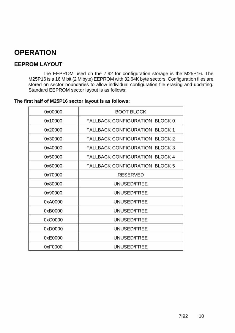
EEPROM LAYOUT
The EEPROM used on the 7I92 for configuration storage is the M25P16. TheM25P16 is a 16 M bit (2 M byte) EEPROM with 32 64K byte sectors. Configuration files arestored on sector boundaries to allow individual configuration file erasing and updating.Standard EEPROM sector layout is as follows:
The first half of M25P16 sector layout is as follows:
0x00000 BOOT BLOCK
0x10000 FALLBACK CONFIGURATION BLOCK 0
0x20000 FALLBACK CONFIGURATION BLOCK 1
0x30000 FALLBACK CONFIGURATION BLOCK 2
0x40000 FALLBACK CONFIGURATION BLOCK 3
0x50000 FALLBACK CONFIGURATION BLOCK 4
0x60000 FALLBACK CONFIGURATION BLOCK 5
0x70000 RESERVED
0x80000 UNUSED/FREE
0x90000 UNUSED/FREE
0xA0000 UNUSED/FREE
0xB0000 UNUSED/FREE
0xC0000 UNUSED/FREE
0xD0000 UNUSED/FREE
0xE0000 UNUSED/FREE
0xF0000 UNUSED/FREE

7I92 11
OPERATION
EEPROM LAYOUT
The second half of M25P16 sector layout is as follows:
0x100000 USER CONFIGURATION BLOCK 0
0x110000 USER CONFIGURATION BLOCK 1
0x120000 USER CONFIGURATION BLOCK 2
0x130000 USER CONFIGURATION BLOCK 3
0x140000 USER CONFIGURATION BLOCK 4
0x150000 USER CONFIGURATION BLOCK 5
0x160000 UNUSED/FREE
0x170000 UNUSED/FREE
0x180000 UNUSED/FREE
0x190000 UNUSED/FREE
0x1A0000 UNUSED/FREE
0x1B0000 UNUSED/FREE
0x1C0000 UNUSED/FREE
0x1D0000 UNUSED/FREE
0x1E0000 UNUSED/FREE
0x1F0000 UNUSED/FREE
7I92 12
OPERATION
BITFILE FORMAT
The configuration utilities expect standard FPGA bitfiles without any multiboot featuresenabled. If multiboot FPGA files are loaded they will likely cause a configuration failure. Inaddition for fallback to work, the -g next_config_register_write:disable, -greset_on_error:enable and -g CRC:enable bitgen options must be set.
WARNING: Never write a bitfile that is not designed for a 7I92 into the 7I92sEEPROM as this will likely "brick" the 7I92 card and require the card to be returnedto Mesa for repair.
MESAFLASH
Linux and Windows utility programs MESAFLASH are provided to writeconfiguration files to the 7I92 EEPROM. These files depend on a simple SPI interface builtinto both the standard user FPGA bitfiles and the fallback bitfile. The MESAFLASH utilitiesexpect standard FPGA bitfiles without any multiboot features enabled. If multiboot FPGAfiles are loaded they will likely cause a configuration failure.
If mesaflash is run with a Bhelp command line argument it will print usageinformation.
The following examples assume the target 7I92 is using the ROM IP address of192.168.1.121.
mesaflash --device 7I92 --write FPGAFILE.BIT
Writes a standard bitfile FPGAFILE.BIT to the user area of the EEPROM.
mesaflash --device 7I92 --verify FPGAFILE.BIT
Verifies the user EEPROM configuration against the bit file FPGAFILE.BIT.
mesaflash --device 7I92 --fallback --write FALLBACK.BIT
Writes the fallback EEPROM configuration to the fallback area of the EEPROM. Inaddition if the bootblock is not present in block 0 of the EEPROM, it re-writes thebootblock.
SETTING EEPROM IP ADDRESSMESAFLASH can also write the EEPROM IP address of the 7I92:
MESAFLASH --device 7I92 --set ip=192.168.0.100
The above examples assume the 7I92 has its default ROM IP address(192.168.1.121). If the 7I92 is using another IP address, this must be specified on thecommand line with a Baddr XX.XX.XX.XX command line argument.
7I92 13
OPERATION
FREE FLASH MEMORY SPACE
Fifteen 64K byte blocks of flash memory space are free when both user and fallbackconfigurations are installed. These free blocks can be used for storing user data.
FALLBACK INDICATION
Mesa’s supplied fallback configurations blink the red INIT LED on the top right handside of the card if the primary configuration fails and the fallback configuration loadedsuccessfully. If this happens it means the user configuration is corrupted or not a properconfiguration for the 7I92s FPGA. This can be fixed by running the configuration utility andre-writing the user configuration.
FAILURE TO CONFIGURE
The 7I92 should configure its FPGA within a fraction of a second of powerapplication. If the FPGA card fails to configure, the red /DONE LED CR2 will remainilluminated. If this happens the 7I92s EEPROM must be re-programmed via the JTAGconnector or (faster) JTAG FPGA load followed by Ethernet EEPROM update.
CLOCK SIGNALS
The 7I92 has a single 50 MHz clock signal from an on card crystal oscillator. Theclock a can be multiplied and divided by the FPGAs clock generator block to generate awide range of internal clock signals. The 50 MHz clock is also used to generate the 25MHzclock for the Ethernet interface chip.
7I92 14
OPERATION
LEDS
The 7I92 has 4 FPGA driven user LEDs (User 0 through User 3 = Green), and 2FPGA driven status LEDs (red) and a power LED. The user LEDs can be used for anypurpose, and can be helpful as a simple debugging feature. A low output signal from theFPGA lights the LED. See the 7I92IO.PIN file for FPGA pin locations of the LED signals.The status LEDs reflect the state of the FPGA’s DONE, and /INIT pins. The /DONE LEDlights until the FPGA is configured at power-up. The /INIT LED lights when the power onreset is asserted, when there has been a CRC error during configuration. When usingMesas configurations, the /INIT LED blinks when the fallback configuration has beenloaded.
PULLUP RESISTORS
All I/O pins are provided with pull-up resistors to allow connection to open drain,open collector, or OPTO devices. These resistors have a value of 4.7K so have amaximum pull-up current of ~1.07 mA (5V pull-up) or ~.7 mA (3.3V pull-up).
IO LEVELS
The Xilinx FPGAs used on the 7I92 have programmable I/O levels for interfacingwith different logic families. The 7I92 does not support use of the I/O standards that requireinput reference voltages. All standard Mesa configurations use LVTTL levels.
Note that even though the 7I92 can tolerate 5V signal inputs, its outputs will notswing to 5V. The outputs are push pull CMOS that will drive to the output supply rail of3.3V. This is sufficient for TTL compatibility but may cause problems with some types ofloads. For example when driving an LED that has its anode connected to 5V, in suchdevices as OPTO isolators and I/O module rack SSRs, the 3.3V high level may notcompletely turn the LED off. To avoid this problem, either drive loads that are groundreferred, Use 3.3V as the VCC for VCC referred loads, or use open drain mode.
STARTUP I/O VOLTAGE
After power-up or system reset and before the the FPGA is configured, the pull-upresistors will pull all I/O signals to a high level. If the FPGA is used for motion control orcontrolling devices that could present a hazard when enabled, external circuitry should bedesigned so that this initial state (high) results in a safe condition.
7I92 15
OPERATION
INTERFACE CABLES
Mesa daughtercards use a male to male DB25 cable to interface to the 7I92. Fornoise immunity and signal fidelity it is suggested that only IEEE-1284 rated cables beused. IEEE-1284 rated cables have a twisted pair shield wire for each signal wire and anoverall shield terminated in the metal connector shell. This results in much betterperformance than flat or NON-IEEE-1284 parallel port cables For short connections of lessthan 3 feet, flat cables can be used. No other type of cable should be used.
Mesa can supply IEEE-1284 cables tested with the 7I92 / daughtercard combinationin 3, 6, and 10 foot lengths.
BREAKOUT POWER OPTION
When used with Mesa breakout/daughter cards, the 7I92 can supply up to 1A of 5Vpower to each of the daughter cards. This option is disabled by default to avoid possibledamage to standard breakout boards, so must be specifically enabled for Mesadaughtercards. If you use this option you must verify that the interface cable does not tiethe eight parallel port ground wires together as some cheap printer cables do. Mesasupplied IEEE-1284 cables are the best option for Mesa daughter cards and areguaranteed to work with the power option. Flat cables will work as well but have poorernoise immunity and signal fidelity.
PLUG AND GO KITS
Motion control kits with pre-programmed 7I92, interface cable, and daughtercard(s)are available to simplify system integration.
7I92 16
SUPPLIED CONFIGURATIONS
HOSTMOT2
All supplied configurations are part of the HostMot2 motion control firmware set. AllHostMot2 firmware is open source and easily extendible to support new interfaces ordifferent sets of interfaces embedded in one configuration. For detailed register levelinformation on Hostmot2 firmware modules, see the regmap file in the hostmot2 sourcecode directory.
7I76X1D
7I76X1D is a configuration intended to work with the 7I76 five axis step/dirdaughtercard. It supports a single 7I76 daughtercard
7I76_7I74D
7I76_7I74 is a configuration for a7I76 five axis step/dir daughtercard on P2 and a7I74 eight channel RS-422 interface on P1, The 7I74 is configured with eight Smart Serialchannels.
G540X2D
G540X2 is a configuration intended to work with two Gecko G540 four axis stepmotor drives. It includes eight hardware step generators, two PWM generators, four GPIOoutputs, eight GPIO inputs, two charge pump drivers and a watchdog timer.
7I77X2D
7I77X2D is a configuration intended to work with the 7I77 six axis analog servodaughtercard. It will support two 7I77 daughtercards. It includes twelve encoder inputs, sixsmart serial interfaces (four used locally on the 7I77s and two fed through for additionalremotes), a watchdog timer and GPIO.
7I77_7I76D
7I77_7I76D is a configuration intended to work with a7I77 six axis analog servodaughtercard on P2 a 7I76 daughtercard on P1.

7I92 17
SUPPLIED CONFIGURATIONS
7I77_7I74D
7I74_7I77D is a configuration intended to work with a7I77 six axis analog servodaughtercard on P2 and a 7I74 eight channel RS-422 interface daughtercard on P1. Itincludes six encoder inputs, 14 smart serial interfaces (2 used on the 7I77 for 48 bitisolated field I/O and analog out) , a watchdog timer and GPIO.
7I74X2D
7I74X2D is a configuration intended to work with two 7I74 RS-422 daughter cardsIt include sixteen smart serial interfaces allowing real time control of up to 784 digital I/Opoints, a watchdog timer and GPIO.
7I78X2D
7I78X2D is a configuration intended to work with the 7I78 four axis step/dirdaughtercard. It will support two 7I78 daughtercards, one on each of the 7I92s I/Oconnectors. The configuration includes eight hardware step generators, two PWMgenerators, two encoder inputs and two Smart Serial interfaces, a watchdog timer andGPIO
PROB_RFX2D
The PROB_RFX2D configuration is a step/dir configuration intended to work withmost common parallel port breakouts. Two breakouts are supported, one on each of the7I92s I/O connectors. The configuration includes eight hardware step generators, twoencoders with index, four PWM generators , a watchdog timer and GPIO.
PIN FILES
Each of the configurations has an associated file with file name extension .pin thatdescribes the FPGA functions included in the configuration and the I/O pinout. These areplain text files that can be printed or viewed with any text editor.
7I92 18
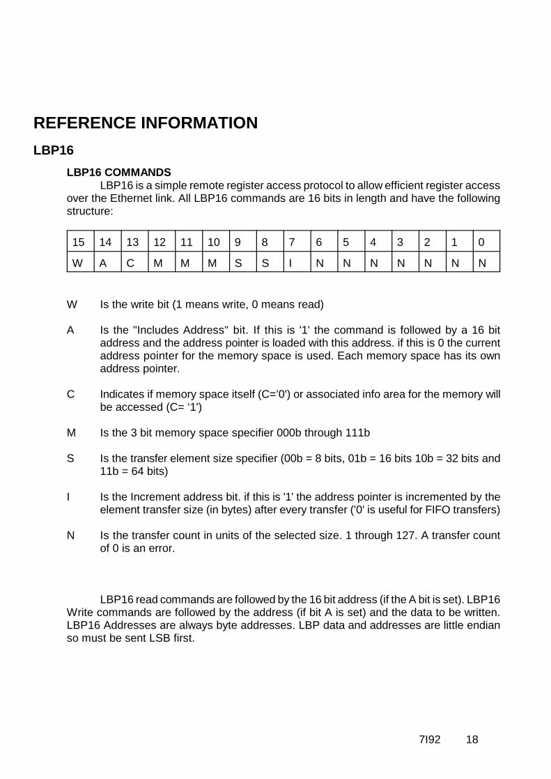
REFERENCE INFORMATION
LBP16
LBP16 COMMANDSLBP16 is a simple remote register access protocol to allow efficient register access
over the Ethernet link. All LBP16 commands are 16 bits in length and have the followingstructure:
15 14 13 12 11 10 9 8 7 6 5 4 3 2 1 0
W A C M M M S S I N N N N N N N
W Is the write bit (1 means write, 0 means read)
A Is the "Includes Address" bit. If this is '1' the command is followed by a 16 bitaddress and the address pointer is loaded with this address. if this is 0 the currentaddress pointer for the memory space is used. Each memory space has its ownaddress pointer.
C Indicates if memory space itself (C=’0') or associated info area for the memory willbe accessed (C= ‘1')
M Is the 3 bit memory space specifier 000b through 111b
S Is the transfer element size specifier (00b = 8 bits, 01b = 16 bits 10b = 32 bits and11b = 64 bits)
I Is the Increment address bit. if this is '1' the address pointer is incremented by theelement transfer size (in bytes) after every transfer ('0' is useful for FIFO transfers)
N Is the transfer count in units of the selected size. 1 through 127. A transfer countof 0 is an error.
LBP16 read commands are followed by the 16 bit address (if the A bit is set). LBP16Write commands are followed by the address (if bit A is set) and the data to be written.LBP16 Addresses are always byte addresses. LBP data and addresses are little endianso must be sent LSB first.

7I92 19
REFERENCE INFORMATION
LBP16
INFO AREAThere are eight possible memory spaces in LBP16. Each memory space has an
associated read only info area. The first entry has a cookie to verify correct access. Thenext two entries in the info area are the MemSizes word and the MemRanges word. Only16 bit read access is allowed to the info area.
0000 COOKIE = 0X5A0N WHERE N = ADDRESS SPACE 0..7
0002 MEMSIZES
0004 MEMRANGES
0006 ADDRESS POINTER
0008 SPACENAME 0,1
000A SPACENAME 2,3
000C SPACENAME 4,5
000E SPACENAME 6,7
INFO AREA MEMSIZES FORMAT
15 14 13 12 11 10 9 8 7 6 5 4 3 2 1 0
W T T T T T T T X X X X A A A A
W Memory space is Writeable
T Is type: 01 = Register, 02 = Memory, 0E = EEPROM, 0F = Flash
A Is access types (bit 0 = 8 bit, bit 1 = 16 bit etc)so for example 0x06 means 16 bitand 32 bit operations allowed

7I92 20
REFERENCE INFORMATION
LBP16
INFO AREA MEMRANGES FORMAT
15 14 13 12 11 10 9 8 7 6 5 4 3 2 1 0
E E E E E P P P P P S S S S S S
E Is erase block size
P Is Page size
S Ps address range
Ranges are 2^E, 2^P, 2^S. All sizes and ranges are in bytes. E and P are 0 for non-flashmemory
7I92 21
REFERENCE INFORMATION
LBP16
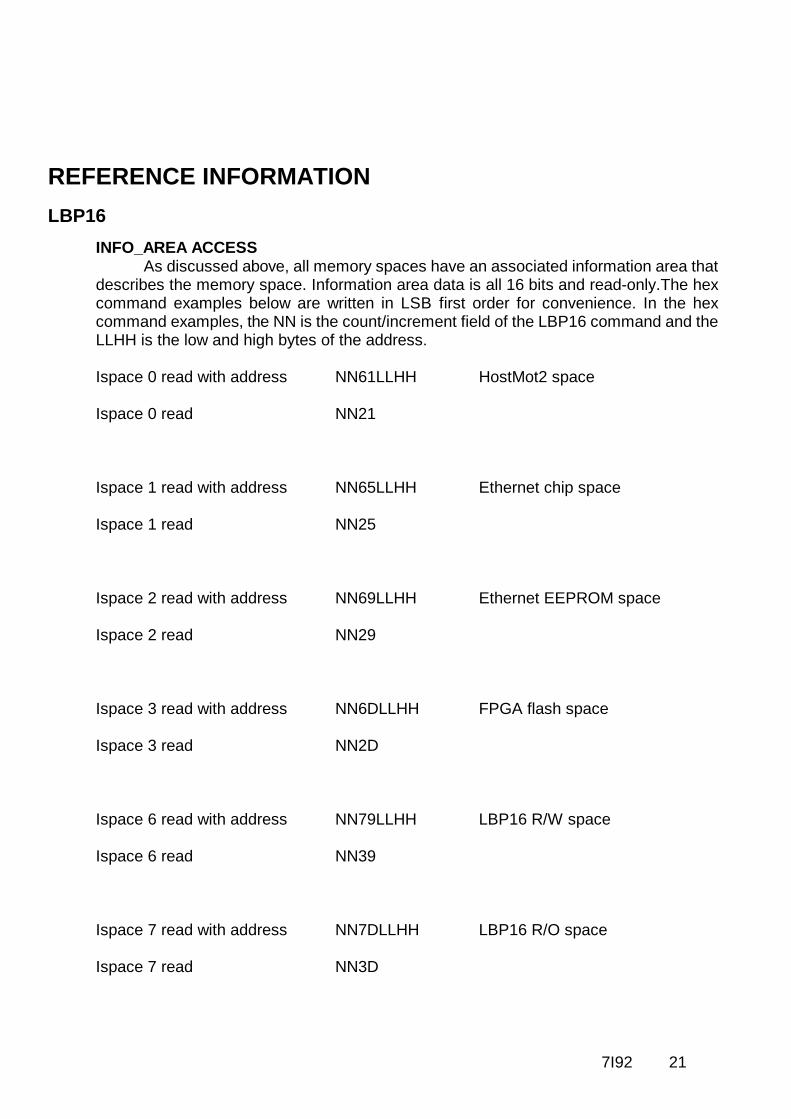
INFO_AREA ACCESSAs discussed above, all memory spaces have an associated information area that
describes the memory space. Information area data is all 16 bits and read-only.The hexcommand examples below are written in LSB first order for convenience. In the hexcommand examples, the NN is the count/increment field of the LBP16 command and theLLHH is the low and high bytes of the address.
Ispace 0 read with address NN61LLHH HostMot2 space
Ispace 0 read NN21
Ispace 1 read with address NN65LLHH Ethernet chip space
Ispace 1 read NN25
Ispace 2 read with address NN69LLHH Ethernet EEPROM space
Ispace 2 read NN29
Ispace 3 read with address NN6DLLHH FPGA flash space
Ispace 3 read NN2D
Ispace 6 read with address NN79LLHH LBP16 R/W space
Ispace 6 read NN39
Ispace 7 read with address NN7DLLHH LBP16 R/O space
Ispace 7 read NN3D

7I92 22
REFERENCE INFORMATION
LBP16
7I92 SUPPORTED MEMORY SPACESThe 7I92 firmware supports 6 address spaces. These will be described individually
with example hexadecimal commands. The hex command examples below are written inLSB first order for convenience. In the hex command examples, the NN is thecount/increment field of the LBP16 command and the LLHH is the low and high bytes ofthe address.
SPACE 0: HOSTMOT2 REGISTERSThis address space is the most important as it gives access to the FPGA I/O. This
is a 64K byte address range space with 32 bit R/W access.
Space 0 read with address NN42LLHH
Space 0 write with address NNC2LLHH
Space 0 read NN02
Space 0 write NN82

7I92 23
REFERENCE INFORMATION
LBP16
SPACE 0: HOSTMOT2 REGISTERSExample: read first 5 entries in hostmot2 IDROM:
85420004
85 ; 85 == NN = 5 | Inc bit (0x80) so address is incremented after eachaccess
42 ; Read from space 0 with address included after command
00 ; LSB of address (IDROM starts at 0x0400)
04 ; MSB of address (IDROM starts at 0x0400)
Example: write 4 GPIO ports starting at 0x1000:
84C20010AAAAAAAABBBBBBBBCCCCCCCCDDDDDDDD
84 ; 84 == NN = 4 | Inc bit so address is incremented after each access
C2 ; Write to space 0 with address included after command
00 ; LSB of address (GPIO starts at 0x1000)
10 ; MSB of address (GPIO starts at 0x1000)
AAAAAAAA ; 32 bit data for GPIO port 0 at 0x1000
BBBBBBBB ; 32 bit data for GPIO port 0 at 0x1004
CCCCCCCC ; 32 bit data for GPIO port 0 at 0x1008
DDDDDDDD ; 32 bit data for GPIO port 0 at 0x100C
Note like all LBP16 data, write data is LS byte first

7I92 24
REFERENCE INFORMATION
LBP16
SPACE 1: ETHERNET CHIP ACCESSSpace 1 allows access to the KSZ8851-16 registers for debug purposes. All
accesses are 16 bit.
Space 1 read with address NN45LLHH
Space 1 write with address NNC5LLHH
Space 1 read NN05
Space 1 write NN85
Example: read Ethernet chip CIDER register: 0145C000
01 ; = NN = read 1 16 bit value
45 ; read space 1 with address included
C0 ; LSB of CIDER address
00 ; MSB of CIDER address
SPACE 2: ETHERNET EEPROM CHIP ACCESSThis space is used to store the Ethernet MAC address, card name, and EEPROM
settable IP address. The Ethernet EEPROM space is accessed as 16 bit data. The first0x20 bytes are read only and the remaining 0x60 bytes are read/write.
Space 2 read with address NN49LLHH
Space 2 write with address NNC9LLHH
Space 2 read NN09
Space 2 write NN89
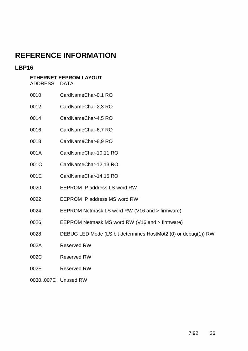
7I92 25
REFERENCE INFORMATION
LBP16
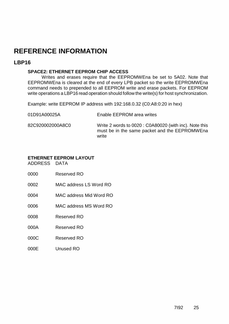
SPACE2: ETHERNET EEPROM CHIP ACCESSWrites and erases require that the EEPROMWEna be set to 5A02. Note that
EEPROMWEna is cleared at the end of every LPB packet so the write EEPROMWEnacommand needs to prepended to all EEPROM write and erase packets. For EEPROMwrite operations a LBP16 read operation should follow the write(s) for host synchronization.
Example: write EEPROM IP address with 192:168.0.32 (C0:A8:0:20 in hex)
01D91A00025A Enable EEPROM area writes
82C920002000A8C0 Write 2 words to 0020 : C0A80020 (with inc). Note thismust be in the same packet and the EEPROMWEnawrite
ETHERNET EEPROM LAYOUTADDRESS DATA
0000 Reserved RO
0002 MAC address LS Word RO
0004 MAC address Mid Word RO
0006 MAC address MS Word RO
0008 Reserved RO
000A Reserved RO
000C Reserved RO
000E Unused RO
7I92 26
REFERENCE INFORMATION
LBP16
ETHERNET EEPROM LAYOUTADDRESS DATA
0010 CardNameChar-0,1 RO
0012 CardNameChar-2,3 RO
0014 CardNameChar-4,5 RO
0016 CardNameChar-6,7 RO
0018 CardNameChar-8,9 RO
001A CardNameChar-10,11 RO
001C CardNameChar-12,13 RO
001E CardNameChar-14,15 RO
0020 EEPROM IP address LS word RW
0022 EEPROM IP address MS word RW
0024 EEPROM Netmask LS word RW (V16 and > firmware)
0026 EEPROM Netmask MS word RW (V16 and > firmware)
0028 DEBUG LED Mode (LS bit determines HostMot2 (0) or debug(1)) RW
002A Reserved RW
002C Reserved RW
002E Reserved RW
0030..007E Unused RW
7I92 27
REFERENCE INFORMATION
LBP16
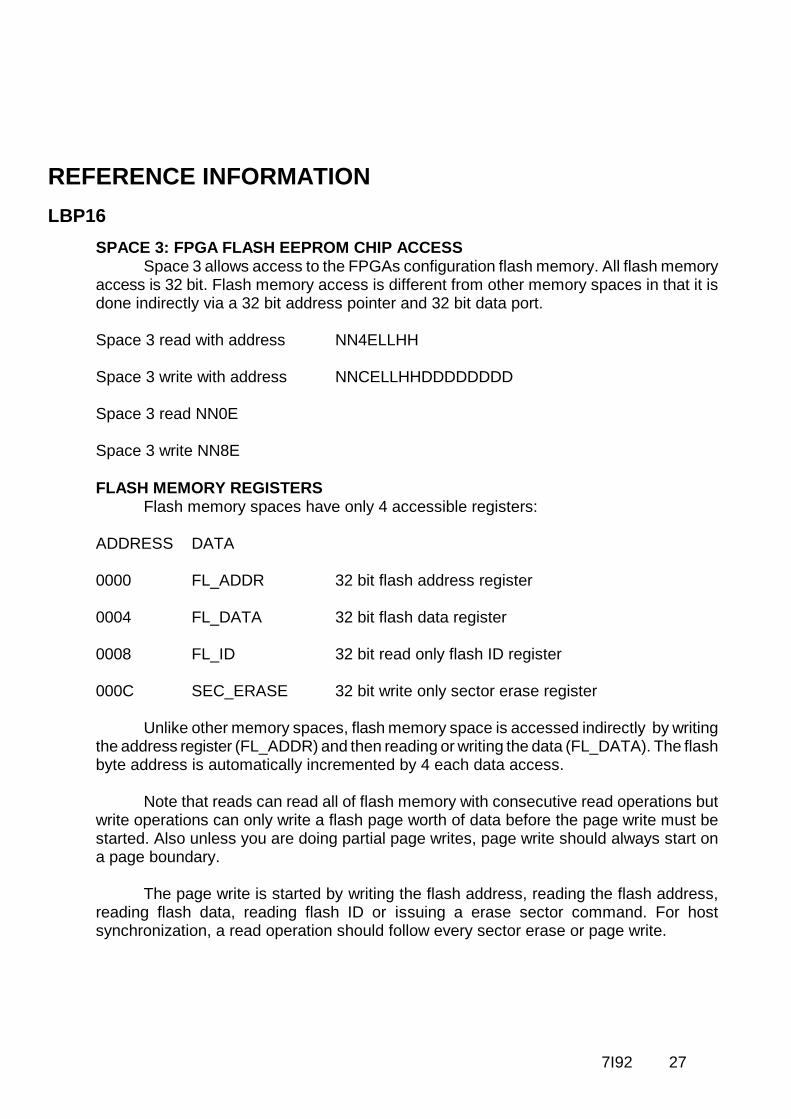
SPACE 3: FPGA FLASH EEPROM CHIP ACCESS Space 3 allows access to the FPGAs configuration flash memory. All flash memory
access is 32 bit. Flash memory access is different from other memory spaces in that it isdone indirectly via a 32 bit address pointer and 32 bit data port.
Space 3 read with address NN4ELLHH
Space 3 write with address NNCELLHHDDDDDDDD
Space 3 read NN0E
Space 3 write NN8E
FLASH MEMORY REGISTERSFlash memory spaces have only 4 accessible registers:
ADDRESS DATA
0000 FL_ADDR 32 bit flash address register
0004 FL_DATA 32 bit flash data register
0008 FL_ID 32 bit read only flash ID register
000C SEC_ERASE 32 bit write only sector erase register
Unlike other memory spaces, flash memory space is accessed indirectly by writingthe address register (FL_ADDR) and then reading or writing the data (FL_DATA). The flashbyte address is automatically incremented by 4 each data access.
Note that reads can read all of flash memory with consecutive read operations butwrite operations can only write a flash page worth of data before the page write must bestarted. Also unless you are doing partial page writes, page write should always start ona page boundary.
The page write is started by writing the flash address, reading the flash address,reading flash data, reading flash ID or issuing a erase sector command. For hostsynchronization, a read operation should follow every sector erase or page write.
7I92 28
REFERENCE INFORMATION
LBP16
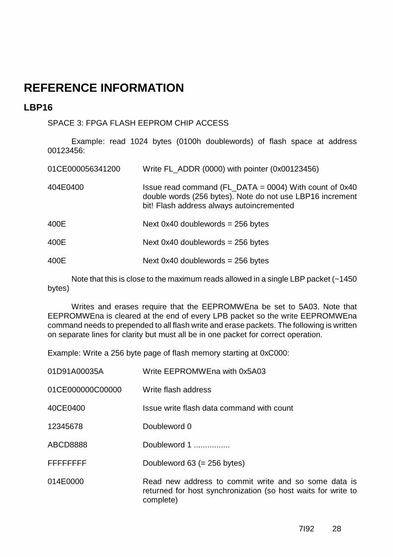
SPACE 3: FPGA FLASH EEPROM CHIP ACCESS
Example: read 1024 bytes (0100h doublewords) of flash space at address00123456:
01CE000056341200 Write FL_ADDR (0000) with pointer (0x00123456)
404E0400 Issue read command (FL_DATA = 0004) With count of 0x40double words (256 bytes). Note do not use LBP16 incrementbit! Flash address always autoincremented
400E Next 0x40 doublewords = 256 bytes
400E Next 0x40 doublewords = 256 bytes
400E Next 0x40 doublewords = 256 bytes
Note that this is close to the maximum reads allowed in a single LBP packet (~1450bytes)
Writes and erases require that the EEPROMWEna be set to 5A03. Note thatEEPROMWEna is cleared at the end of every LPB packet so the write EEPROMWEnacommand needs to prepended to all flash write and erase packets. The following is writtenon separate lines for clarity but must all be in one packet for correct operation.
Example: Write a 256 byte page of flash memory starting at 0xC000:
01D91A00035A Write EEPROMWEna with 0x5A03
01CE000000C00000 Write flash address
40CE0400 Issue write flash data command with count
12345678 Doubleword 0
ABCD8888 Doubleword 1 ................
FFFFFFFF Doubleword 63 (= 256 bytes)
014E0000 Read new address to commit write and so some data isreturned for host synchronization (so host waits for write tocomplete)
7I92 29
REFERENCE INFORMATION
LBP16
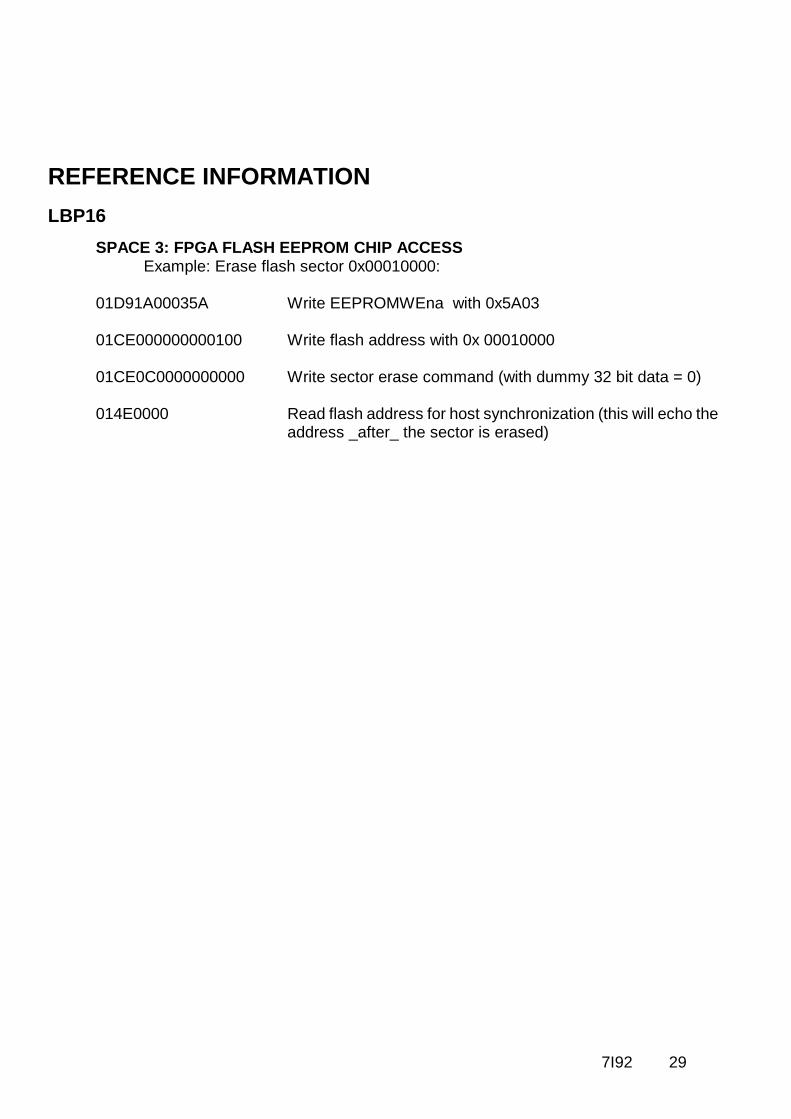
SPACE 3: FPGA FLASH EEPROM CHIP ACCESSExample: Erase flash sector 0x00010000:
01D91A00035A Write EEPROMWEna with 0x5A03
01CE000000000100 Write flash address with 0x 00010000
01CE0C0000000000 Write sector erase command (with dummy 32 bit data = 0)
014E0000 Read flash address for host synchronization (this will echo theaddress _after_ the sector is erased)

7I92 30
REFERENCE INFORMATION
LBP16
SPACE 4 LBP TIMER/UTILITY AREAAddress space 4 is for read/write access to LBP specific timing registers. All
memory space 4 access is 16 bit.
Space 4 read with address NN51LLHH
Space 4 write with address NND1LLHHDDDD
Space 4 read NN11
Space 4 write NN91DDDD
MEMORY SPACE 4 LAYOUT: ADDRESS DATA
0000 uSTimeStampReg
0002 WaituSReg
0004 HM2Timeout
0006 WaitForHM2RefTime
0008 WaitForHM2Timer1
000A WaitForHM2Timer2
000C WaitForHM2Timer3
000E WaitForHM2Timer4
0010..001E Scratch registers for any use
The uSTimeStamp register reads the free running hardware microsecond timer. Itis useful for timing internal 7I92 operations. Writes to the uSTimeStamp register are a no-op. The WaituS register delays processing for the specified number of microseconds whenwritten, (0 to 65535 uS) reads return the last wait time written. The HM2TimeOut registersets the timeout value for all WaitForHM2 times (0 to 65536 uS).
All the WaitForHM2Timer registers wait for the rising edge of the specified timer orreference output when read or written, write data is don’t care, and reads return the waittime in uS. The HM2TimeOut register places an upper bound on how long the WaitForHM2operations will wait. HM2Timeouts set the HM2TImeout error bit in the error register.
7I92 31
REFERENCE INFORMATION
LBP16
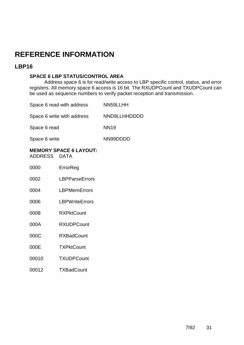
SPACE 6 LBP STATUS/CONTROL AREAAddress space 6 is for read/write access to LBP specific control, status, and error
registers. All memory space 6 access is 16 bit. The RXUDPCount and TXUDPCount canbe used as sequence numbers to verify packet reception and transmission.
Space 6 read with address NN59LLHH
Space 6 write with address NND9LLHHDDDD
Space 6 read NN19
Space 6 write NN99DDDD
MEMORY SPACE 6 LAYOUT: ADDRESS DATA
0000 ErrorReg
0002 LBPParseErrors
0004 LBPMemErrors
0006 LBPWriteErrors
0008 RXPktCount
000A RXUDPCount
000C RXBadCount
000E TXPktCount
00010 TXUDPCount
00012 TXBadCount

7I92 32
REFERENCE INFORMATION
LBP16
MEMORY SPACE 6 LAYOUT:ADDRESS DATA
0014 LEDMode If LSb is 0, LEDs are "owned" by HostMot2,otherwise LEDs are local debug LEDs
0016 DebugLEDPtr What variable in space 6 local debug LEDs show(default is RXPktCount).
0018 Scratch Can be used for sequence numbers
001A EEPROMWEna Must be set to 5A0N to enable EEPROM or flashwrites or erases (N is memory space ofEEPROM or flash) Note that this is cleared atthe end of every packet.
001C LBPReset Setting this to a non-zero value will do a fullreset of the LBP16 firmware. The 7I92 will readits IP address jumpers and re-assign its IPaddress. The 7I92 will be unresponsive for asmuch as ½ of a second after this command.
001E FPGAICAP FPGA ICAP-16 register to allow remote FPGAreload and other low level FPGA access.
ERROR REGISTER FORMATBIT ERROR
0 LBPParseError
1 LBPMemError
2 LBPWriteError
3 RXPacketErr
4 TXPacketErr
5 HM2TimeOutError
6..15 Reserved

7I92 33
REFERENCE INFORMATION
LBP16
SPACE 7: LBP READ ONLY AREAMemory space 7 is used for read only card information. Memory space 7 is
accessed as 16 bit data.
Space 7 read with address NN5DLLHH
Space 7 read NN1D
MEMORY SPACE 7 LAYOUT:ADDRESS DATA
0000 CardNameChar-0,1
0002 CardNameChar-2,3
0004 CardNameChar-4,5
0006 CardNameChar-6,7
0008 CardNameChar-8,9
000A CardNameChar-10,11
000C CardNameChar-12.13
000E CardNameChar-14,15
0010 LBPVersion
0012 FirmwareVersion
0014 Option Jumpers
0016 Reserved
0018 RecvStartTS 1 uSec timestamps
001A RecvDoneTS For performance monitoring
001C SendStartTS Send timestamps are
001E SendDoneTS from previous packet
7I92 34
REFERENCE INFORMATION
LBP16
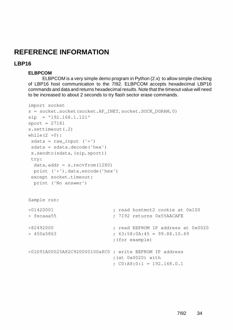
ELBPCOMELBPCOM is a very simple demo program in Python (2.x) to allow simple checking
of LBP16 host communication to the 7I92. ELBPCOM accepts hexadecimal LBP16commands and data and returns hexadecimal results. Note that the timeout value will needto be increased to about 2 seconds to try flash sector erase commands.
import sockets = socket.socket(socket.AF_INET,socket.SOCK_DGRAM, 0)sip = "192.168.1.121"sport = 27181s.settimeout(.2)while(2 >0): sdata = raw_input ('>') sdata = sdata.decode('hex') s.sendto(sdata,(sip,sport)) try: data,addr = s.recvfrom(1280) print ('>'),data.encode('hex') except socket.timeout: print ('No answer')
Sample run:
>01420001 ; read hostmot2 cookie at 0x100> fecaaa55 ; 7I92 returns 0x55AACAFE
>82492000 ; read EEPROM IP address at 0x0020> 450a5863 ; 63:58:0A:45 = 99.88.10.69
;(for example)
>01D91A00025A82C920000100a8C0 ; write EEPROM IP addr ess ;(at 0x0020) with ; C0:A8:0:1 = 192.168.0.1

7I92 35
REFERENCE
SPECIFICATIONS
POWER MIN MAX NOTES:
5V POWER SUPPLY 4.5V 5.5V P3 supplied 5V
5V POWER CONSUMPTION: ---- 2A P3 Connector limit,a c t u a l c u r r e n tdepends on external5V load.
5V POWER CONSUMPTION: ---- 250 mA No external load
MAX 5V CURRENT TO I/O CONNS ---- 1000 mA Each (PTC Limit)
TEMPERATURE RANGE -C version 0 oC +70 oC
TEMPERATURE RANGE -I version -40 oC +85 oC
INPUT VOLTAGE 5V TOL MODE -0.3V 7V
INPUT VOLTAGE 3.3V TOL MODE -0.3V 4V
OUTPUT VOLTAGE 24 MA SINK ---- 0.6V FPGA outputs setfor 24 MA drive
OUTPUT VOLTAGE 24 MA SOURCE 2.4V ---- FPGA outputs setfor 24 MA drive

7I92 36
REFERENCE INFORMATION
CARD DRAWING