72 Technology focus: Micro-LEDs Increased current for red ...
3
K ing Abdullah University of Science and Technology (KAUST) in Saudi Arabia has reported indium gallium nitride (InGaN) red micro-sized light-emitting diodes (μLEDs) aimed at meeting the color and power requirements of LED-based displays [Zhe Zhuang et al, Photonics Research, v9, p1796, 2021]. In particular, the researchers compared the color performance of red, green and blue (RGB) InGaN μLED arrays with that required by the International Telecom- munication Union Radiocommunication Sector (ITU-R) Recommendation BT.2020 (Rec.2020), ‘Parameter values for ultra-high definition television systems for production and international programme exchange’. Although blue and green InGaN LEDs are reaching commercialization, the red sector is still very much “in development” with red InGaN LEDs generally suffering from very low efficiency and output power, compared with devices based on aluminium gallium indium phosphide (AlGaInP) technology. However, the AlGaInP LED performance does not scale well to the micro-level. This is attributed to material problems, in particular high surface recombination velocities and longer carrier diffusion lengths. As devices become smaller, surface effects come to dominate. Surface carrier recombination tends to be non-radiative, sapping output power. By contrast, the performance of InGaN red μLEDs has been found to be only slightly impacted by scaling to the micro-level. Displays based on mixing RGB light from μLEDs is desired from the perspectives of fast response, long lifetime, high brightness level, and low energy con- sumption. The KAUST red InGaN structure was grown by metal-organic vapor phase epitaxy (MOVPE) on patterned sapphire at 100kPa pressure. The active region consisted of two red-emitting quantum wells (QWs) and one blue-emitting quantum well. The 24nm barriers between the wells used a multi-layer AlN/GaN/AlGaN/GaN structure in an effort to compensate for strain imbalances. The presence of Technology focus: Micro-LEDs semiconductorTODAY Compounds&AdvancedSilicon • Vol. 16 • Issue 8 • October 2021 www.semiconductor-today.com 72 Increased current for red InGaN micro-LEDs Researchers have achieved power density comparable to AlGaInP devices targeting display applications. Figure 1. (a) Cross-sectional scanning transmission electron microscopy (STEM) image of red InGaN LED structures. (b)–(d) Energy-dispersive x-ray spectroscopy (EDS) elemental mappings of In, Al and Ga atoms in InGaN QWs and SLs. (e) Top-view and (f) high-resolution scanning electron microscopy (SEM) images for red μLED array. (g) Cross-sectional TEM image of single μLED. (h)–(j) Cross-sectional high-resolution TEM (HRTEM) images of interfaces between nitride materials and SiO 2 .
Transcript of 72 Technology focus: Micro-LEDs Increased current for red ...

King Abdullah University of Science and Technology(KAUST) in Saudi Arabia has reported indium gallium nitride (InGaN) red micro-sized
light-emitting diodes (µLEDs) aimed at meeting thecolor and power requirements of LED-based displays[Zhe Zhuang et al, Photonics Research, v9, p1796, 2021].In particular, the researchers compared the color performance of red, green and blue (RGB) InGaN µLEDarrays with that required by the International Telecom-munication Union Radiocommunication Sector (ITU-R)Recommendation BT.2020 (Rec.2020), ‘Parameter values for ultra-high definition television systems forproduction and international programme exchange’. Although blue and green InGaN LEDs are reaching
commercialization, the red sector is still very much “in development” with red InGaN LEDs generally suffering from very low efficiency and output power,compared with devices based on aluminium galliumindium phosphide (AlGaInP) technology. However, theAlGaInP LED performance does not scale well to the
micro-level. This is attributed to material problems, in particular high surface recombination velocities andlonger carrier diffusion lengths. As devices becomesmaller, surface effects come to dominate. Surface carrier recombination tends to be non-radiative, sapping output power. By contrast, the performance of InGaN red µLEDs has been found to be only slightlyimpacted by scaling to the micro-level.Displays based on mixing RGB light from µLEDs is
desired from the perspectives of fast response, longlifetime, high brightness level, and low energy con-sumption.The KAUST red InGaN structure was grown by
metal-organic vapor phase epitaxy (MOVPE) on patterned sapphire at 100kPa pressure. The activeregion consisted of two red-emitting quantum wells(QWs) and one blue-emitting quantum well. The 24nm barriers between the wells used a multi-layerAlN/GaN/AlGaN/GaN structure in an effort to compensate for strain imbalances. The presence of
Technology focus: Micro-LEDs
semiconductorTODAY Compounds&AdvancedSilicon • Vol. 16 • Issue 8 • October 2021 www.semiconductor-today.com
72
Increased current for red InGaN micro-LEDs Researchers have achieved power density comparable to AlGaInP devicestargeting display applications.
Figure 1. (a) Cross-sectional scanning transmission electron microscopy (STEM) image of red InGaN LEDstructures. (b)–(d) Energy-dispersive x-ray spectroscopy (EDS) elemental mappings of In, Al and Ga atomsin InGaN QWs and SLs. (e) Top-view and (f) high-resolution scanning electron microscopy (SEM) images forred µLED array. (g) Cross-sectional TEM image of single µLED. (h)–(j) Cross-sectional high-resolution TEM(HRTEM) images of interfaces between nitride materials and SiO2.
aluminium (Al) in the barrier also inhibited indiumevaporation from wells during high-temperature growth.A 15-period InGaN/GaN superlattice (SL) was placedunder the active region. The µLEDs were fabricated with indium tin oxide
(ITO) as a transparent conductor on the p-side on thedevice (Figure 1). The ITO layer was annealed in atwo-step process. Then the 17µmx17µm device mesawas plasma etched using plasma-enhanced chemicalvapor deposition (PECVD) silicon dioxide (SiO2) as ahard mask. The mesa sidewalls were treated withtetramethylammonium hydroxide (TMAH) wet-etchingto remove surface damage from the plasma etchprocess.The SiO2 hard mask residue was removed with
buffered oxide etch and replaced with a new layer of PECVD SiO2 as a sidewall passivation layer and electrical isolation. The n- and p-electrodes consisted ofchromium/platinum/gold connected through the SiO2.The devices were connected in 10x10 arrays, using thesame metal combination as for the electrodes. Greenand blue 10x10 structures were also fabricated usingcommercial LED wafers. The turn-on voltage was around 2V, while there was
quite a high current leakage under reverse bias: 7.8µAor 0.27mA/cm2 at –4V. The leakage was blamed on the“many defects/dislocations generated in high-indium-content QWs”, as needed for red emission.At 50A/cm2 injection, the electroluminescence spectra
showed a single red peak at 630nm with 62.9nm full-width at half-maximum (FWHM). At lower 10A/cm2
injection, the peak exhibited a shoulder, which theresearchers attribute tentatively to “localized states,which originated from the indium phase separation inhigh-indium-content QWs.” The 630nm wavelengthmeets the Rec.2020 requirement for red primary coloremission. Between the two current levels there was a large
32nm blue-shift with the increased injection, mainlydue to “strong quantum-confined Stark effect (QCSE)and band-filling effect in red InGaN QWs.” Otherresearch on red InGaN tends to see similar shifts. Thewidth of the peak also reduced with increased currentdue to the emission from localized states saturating.The localized states have more varied emission wave-lengths, relative to band-to-band recombination.The 50A/cm2 emission at 630nm was at a much
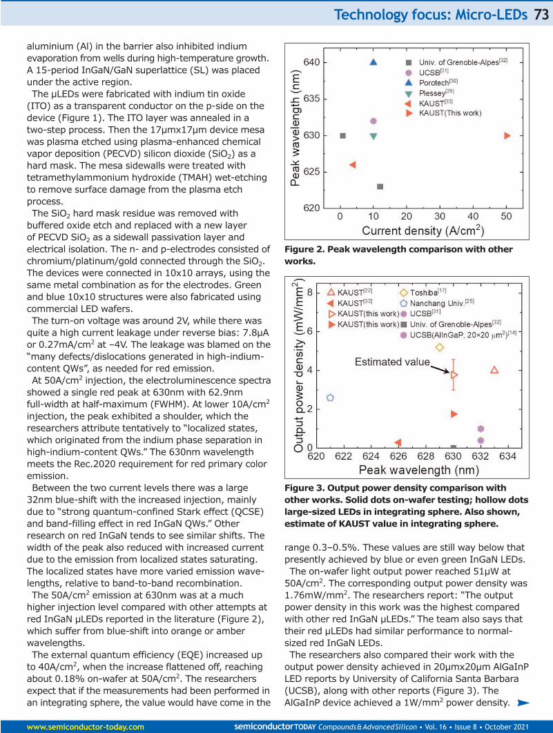
higher injection level compared with other attempts atred InGaN µLEDs reported in the literature (Figure 2),which suffer from blue-shift into orange or amberwavelengths.The external quantum efficiency (EQE) increased up
to 40A/cm2, when the increase flattened off, reachingabout 0.18% on-wafer at 50A/cm2. The researchersexpect that if the measurements had been performed inan integrating sphere, the value would have come in the
range 0.3–0.5%. These values are still way below thatpresently achieved by blue or even green InGaN LEDs.The on-wafer light output power reached 51µW at
50A/cm2. The corresponding output power density was1.76mW/mm2. The researchers report: “The outputpower density in this work was the highest comparedwith other red InGaN µLEDs.” The team also says thattheir red µLEDs had similar performance to normal-sized red InGaN LEDs. The researchers also compared their work with the
output power density achieved in 20µmx20µm AlGaInPLED reports by University of California Santa Barbara(UCSB), along with other reports (Figure 3). TheAlGaInP device achieved a 1W/mm2 power density.
Technology focus: Micro-LEDs
www.semiconductor-today.com semiconductorTODAY Compounds&AdvancedSilicon • Vol. 16 • Issue 8 • October 2021
73
Figure 2. Peak wavelength comparison with otherworks.
Figure 3. Output power density comparison withother works. Solid dots on-wafer testing; hollow dotslarge-sized LEDs in integrating sphere. Also shown,estimate of KAUST value in integrating sphere.
Technology focus: Micro-LEDs
semiconductorTODAY Compounds&AdvancedSilicon • Vol. 16 • Issue 8 • October 2021 www.semiconductor-today.com
74
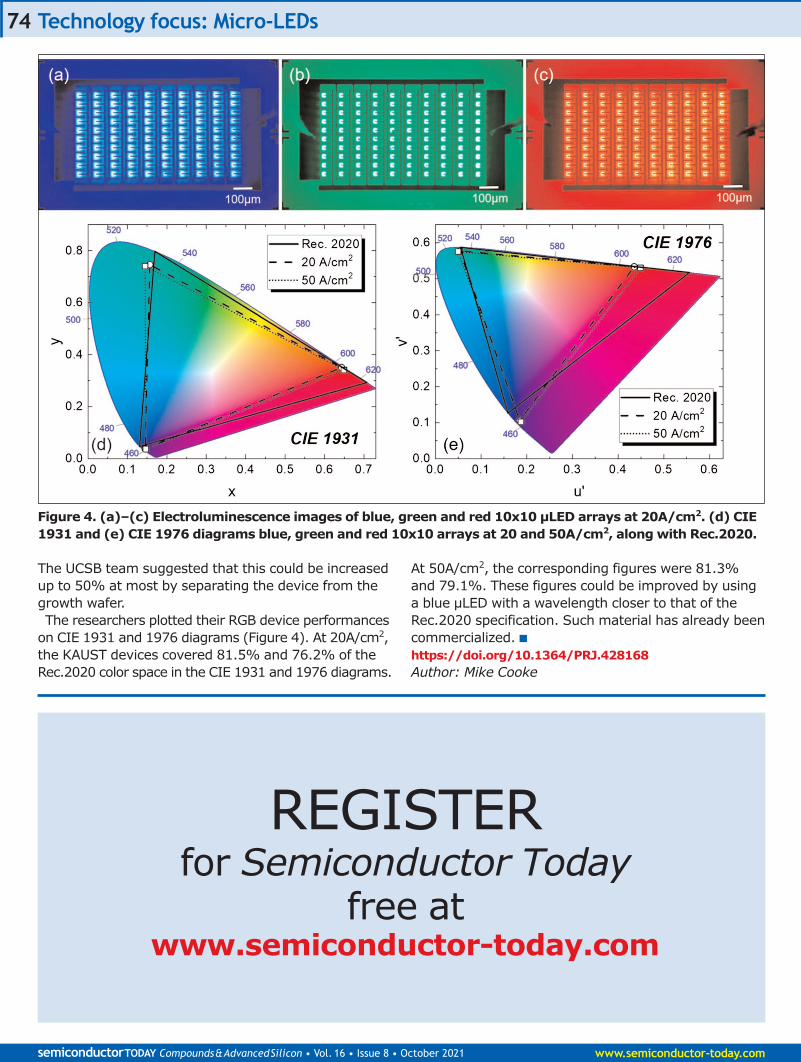
The UCSB team suggested that this could be increasedup to 50% at most by separating the device from thegrowth wafer.The researchers plotted their RGB device performances
on CIE 1931 and 1976 diagrams (Figure 4). At 20A/cm2,the KAUST devices covered 81.5% and 76.2% of theRec.2020 color space in the CIE 1931 and 1976 diagrams.
At 50A/cm2, the corresponding figures were 81.3%and 79.1%. These figures could be improved by usinga blue µLED with a wavelength closer to that of theRec.2020 specification. Such material has already beencommercialized. ■
https://doi.org/10.1364/PRJ.428168Author: Mike Cooke
Figure 4. (a)–(c) Electroluminescence images of blue, green and red 10x10 µLED arrays at 20A/cm2. (d) CIE1931 and (e) CIE 1976 diagrams blue, green and red 10x10 arrays at 20 and 50A/cm2, along with Rec.2020.
REGISTERfor Semiconductor Today
free at www.semiconductor-today.com