7. System Clock and Clock Options
21
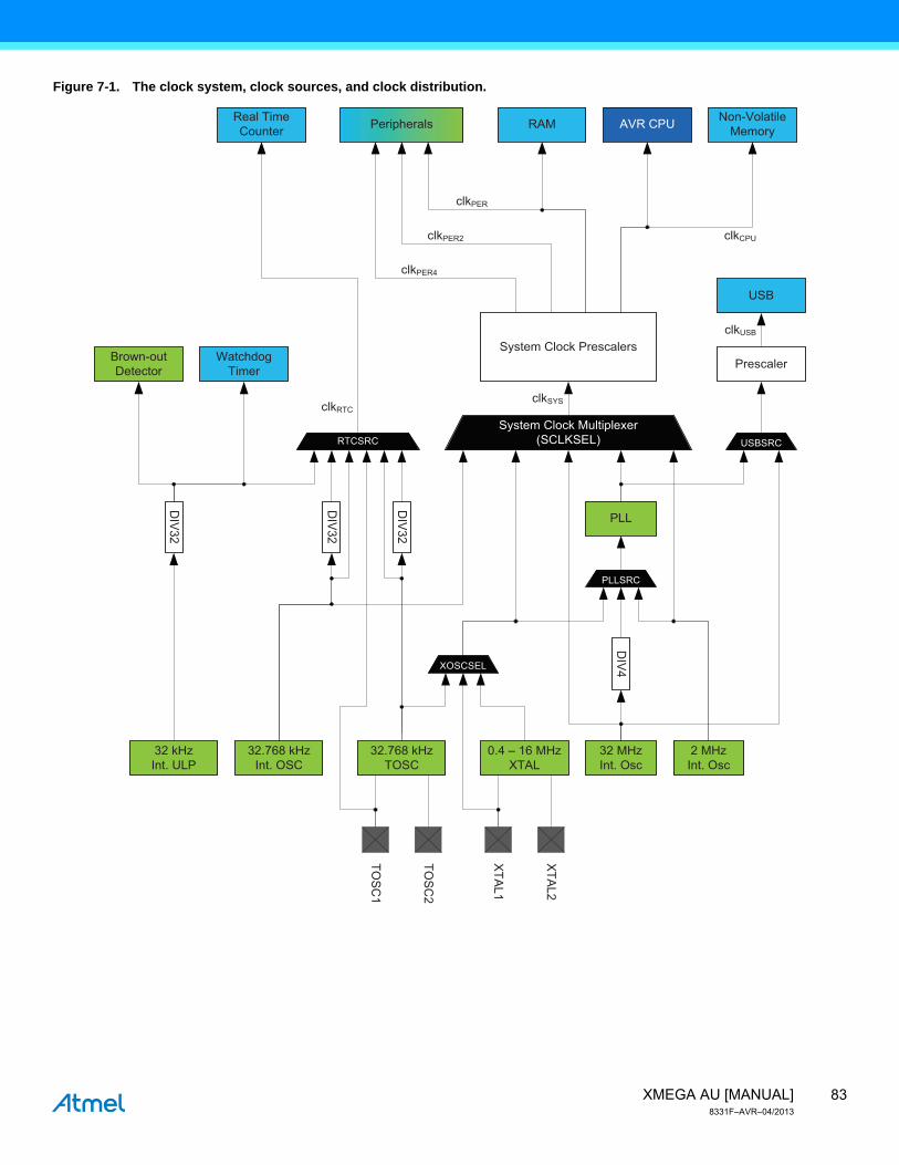
82 XMEGA AU [MANUAL] 8331F–AVR–04/2013 7. System Clock and Clock Options 7.1 Features Fast start-up time Safe run-time clock switching Internal oscillators: 32MHz run-time calibrated oscillator 2MHz run-time calibrated oscillator 32.768kHz calibrated oscillator 32kHz ultra low power (ULP) oscillator with 1kHz output External clock options 0.4MHz - 16MHz crystal oscillator 32.768kHz crystal oscillator External clock PLL with 20MHz - 128MHz output frequency Internal and external clock options and 1x to 31x multiplication Lock detector Clock prescalers with 1x to 2048x division Fast peripheral clocks running at 2 and 4 times the CPU clock Automatic run-time calibration of internal oscillators External oscillator and PLL lock failure detection with optional non-maskable interrupt 7.2 Overview XMEGA devices have a flexible clock system supporting a large number of clock sources. It incorporates both accurate internal oscillators and external crystal oscillator and resonator support. A high-frequency phase locked loop (PLL) and clock prescalers can be used to generate a wide range of clock frequencies. A calibration feature (DFLL) is available, and can be used for automatic run-time calibration of the internal oscillators to remove frequency drift over voltage and temperature. An oscillator failure monitor can be enabled to issue a non-maskable interrupt and switch to the internal oscillator if the external oscillator or PLL fails. When a reset occurs, all clock sources except the 32kHz ultra low power oscillator are disabled. After reset, the device will always start up running from the 2MHz internal oscillator. During normal operation, the system clock source and prescalers can be changed from software at any time. Figure 7-1 on page 83 presents the principal clock system in the XMEGA family of devices. Not all of the clocks need to be active at a given time. The clocks for the CPU and peripherals can be stopped using sleep modes and power reduction registers, as described in “Power Management and Sleep Modes” on page 103.
Transcript of 7. System Clock and Clock Options
82XMEGA AU [MANUAL]8331F–AVR–04/2013
7. System Clock and Clock Options
7.1 Features Fast start-up time
Safe run-time clock switching
Internal oscillators: 32MHz run-time calibrated oscillator 2MHz run-time calibrated oscillator 32.768kHz calibrated oscillator 32kHz ultra low power (ULP) oscillator with 1kHz output
External clock options 0.4MHz - 16MHz crystal oscillator 32.768kHz crystal oscillator External clock
PLL with 20MHz - 128MHz output frequency Internal and external clock options and 1x to 31x multiplication Lock detector
Clock prescalers with 1x to 2048x division
Fast peripheral clocks running at 2 and 4 times the CPU clock
Automatic run-time calibration of internal oscillators
External oscillator and PLL lock failure detection with optional non-maskable interrupt
7.2 Overview
XMEGA devices have a flexible clock system supporting a large number of clock sources. It incorporates both accurate internal oscillators and external crystal oscillator and resonator support. A high-frequency phase locked loop (PLL) and clock prescalers can be used to generate a wide range of clock frequencies. A calibration feature (DFLL) is available, and can be used for automatic run-time calibration of the internal oscillators to remove frequency drift over voltage and temperature. An oscillator failure monitor can be enabled to issue a non-maskable interrupt and switch to the internal oscillator if the external oscillator or PLL fails.
When a reset occurs, all clock sources except the 32kHz ultra low power oscillator are disabled. After reset, the device will always start up running from the 2MHz internal oscillator. During normal operation, the system clock source and prescalers can be changed from software at any time.
Figure 7-1 on page 83 presents the principal clock system in the XMEGA family of devices. Not all of the clocks need to be active at a given time. The clocks for the CPU and peripherals can be stopped using sleep modes and power reduction registers, as described in “Power Management and Sleep Modes” on page 103.
83XMEGA AU [MANUAL]8331F–AVR–04/2013
Figure 7-1. The clock system, clock sources, and clock distribution.
Real TimeCounter Peripherals RAM AVR CPU Non-Volatile
Memory
WatchdogTimer
Brown-outDetector
System Clock Prescalers
USB
Prescaler
System Clock Multiplexer(SCLKSEL)
PLLSRC
RTCSRC
DIV32
32 kHzInt. ULP
32.768 kHzInt. OSC
32.768 kHzTOSC
2 MHzInt. Osc
32 MHzInt. Osc
0.4 – 16 MHzXTAL
DIV32
DIV32
DIV4XOSCSEL
PLL
USBSRC
TOSC
1
TOSC
2
XTAL1
XTAL2
clkSYSclkRTC
clkPER2
clkPER
clkCPU
clkPER4
clkUSB
84XMEGA AU [MANUAL]8331F–AVR–04/2013
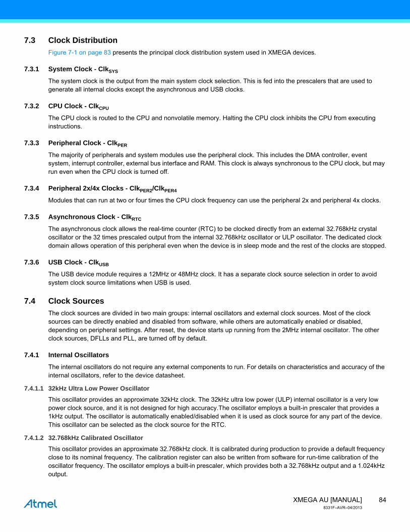
7.3 Clock Distribution
Figure 7-1 on page 83 presents the principal clock distribution system used in XMEGA devices.
7.3.1 System Clock - ClkSYS
The system clock is the output from the main system clock selection. This is fed into the prescalers that are used to generate all internal clocks except the asynchronous and USB clocks.
7.3.2 CPU Clock - ClkCPU
The CPU clock is routed to the CPU and nonvolatile memory. Halting the CPU clock inhibits the CPU from executing instructions.
7.3.3 Peripheral Clock - ClkPER
The majority of peripherals and system modules use the peripheral clock. This includes the DMA controller, event system, interrupt controller, external bus interface and RAM. This clock is always synchronous to the CPU clock, but may run even when the CPU clock is turned off.
7.3.4 Peripheral 2x/4x Clocks - ClkPER2/ClkPER4
Modules that can run at two or four times the CPU clock frequency can use the peripheral 2x and peripheral 4x clocks.
7.3.5 Asynchronous Clock - ClkRTC
The asynchronous clock allows the real-time counter (RTC) to be clocked directly from an external 32.768kHz crystal oscillator or the 32 times prescaled output from the internal 32.768kHz oscillator or ULP oscillator. The dedicated clock domain allows operation of this peripheral even when the device is in sleep mode and the rest of the clocks are stopped.
7.3.6 USB Clock - ClkUSB
The USB device module requires a 12MHz or 48MHz clock. It has a separate clock source selection in order to avoid system clock source limitations when USB is used.
7.4 Clock Sources
The clock sources are divided in two main groups: internal oscillators and external clock sources. Most of the clock sources can be directly enabled and disabled from software, while others are automatically enabled or disabled, depending on peripheral settings. After reset, the device starts up running from the 2MHz internal oscillator. The other clock sources, DFLLs and PLL, are turned off by default.
7.4.1 Internal Oscillators
The internal oscillators do not require any external components to run. For details on characteristics and accuracy of the internal oscillators, refer to the device datasheet.
7.4.1.1 32kHz Ultra Low Power Oscillator
This oscillator provides an approximate 32kHz clock. The 32kHz ultra low power (ULP) internal oscillator is a very low power clock source, and it is not designed for high accuracy.The oscillator employs a built-in prescaler that provides a 1kHz output. The oscillator is automatically enabled/disabled when it is used as clock source for any part of the device. This oscillator can be selected as the clock source for the RTC.
7.4.1.2 32.768kHz Calibrated Oscillator
This oscillator provides an approximate 32.768kHz clock. It is calibrated during production to provide a default frequency close to its nominal frequency. The calibration register can also be written from software for run-time calibration of the oscillator frequency. The oscillator employs a built-in prescaler, which provides both a 32.768kHz output and a 1.024kHz output.
85XMEGA AU [MANUAL]8331F–AVR–04/2013
7.4.1.3 32MHz Run-time Calibrated Oscillator
The 32MHz run-time calibrated internal oscillator is a high-frequency oscillator. It is calibrated during production to provide a default frequency close to its nominal frequency. A digital frequency looked loop (DFLL) can be enabled for automatic run-time calibration of the oscillator to compensate for temperature and voltage drift and optimize the oscillator accuracy. This oscillator can also be adjusted and calibrated to any frequency between 30MHz and 55MHz. The production signature row contains 48 MHz calibration values intended used when the oscillator is used a full-speed USB clock source.
7.4.1.4 2MHz Run-time Calibrated Oscillator
The 2MHz run-time calibrated internal oscillator is the default system clock source after reset. It is calibrated during production to provide a default frequency close to its nominal frequency. A DFLL can be enabled for automatic run-time calibration of the oscillator to compensate for temperature and voltage drift and optimize the oscillator accuracy.
7.4.2 External Clock Sources
The XTAL1 and XTAL2 pins can be used to drive an external oscillator, either a quartz crystal or a ceramic resonator. XTAL1 can be used as input for an external clock signal. The TOSC1 and TOSC2 pins is dedicated to driving a 32.768kHz crystal oscillator.
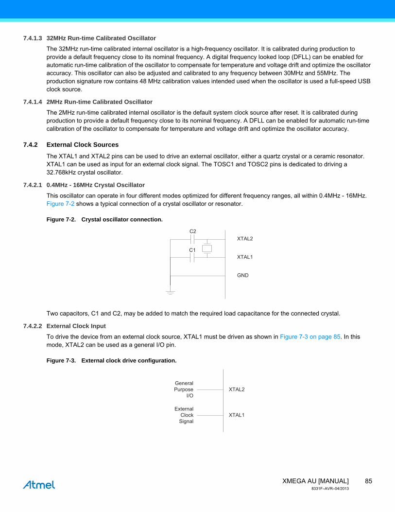
7.4.2.1 0.4MHz - 16MHz Crystal Oscillator
This oscillator can operate in four different modes optimized for different frequency ranges, all within 0.4MHz - 16MHz. Figure 7-2 shows a typical connection of a crystal oscillator or resonator.
Figure 7-2. Crystal oscillator connection.
Two capacitors, C1 and C2, may be added to match the required load capacitance for the connected crystal.
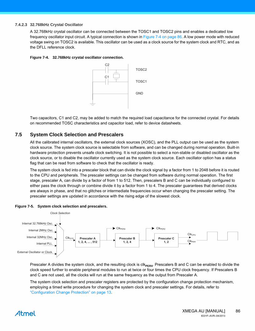
7.4.2.2 External Clock Input
To drive the device from an external clock source, XTAL1 must be driven as shown in Figure 7-3 on page 85. In this mode, XTAL2 can be used as a general I/O pin.
Figure 7-3. External clock drive configuration.
C1
C2XTAL2
XTAL1
GND
General Purpose
I/OXTAL2
XTAL1External
ClockSignal
86XMEGA AU [MANUAL]8331F–AVR–04/2013
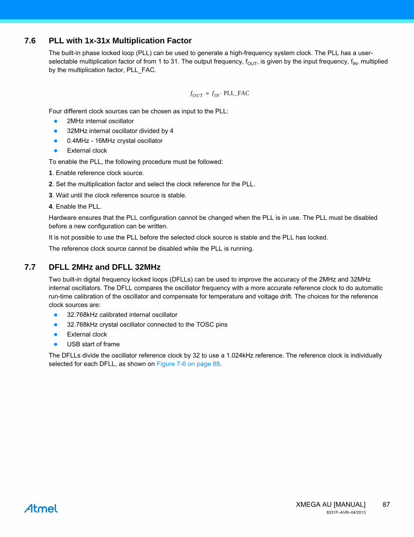
7.4.2.3 32.768kHz Crystal Oscillator
A 32.768kHz crystal oscillator can be connected between the TOSC1 and TOSC2 pins and enables a dedicated low frequency oscillator input circuit. A typical connection is shown in Figure 7-4 on page 86. A low power mode with reduced voltage swing on TOSC2 is available. This oscillator can be used as a clock source for the system clock and RTC, and as the DFLL reference clock.
Figure 7-4. 32.768kHz crystal oscillator connection.
Two capacitors, C1 and C2, may be added to match the required load capacitance for the connected crystal. For details on recommended TOSC characteristics and capacitor load, refer to device datasheets.
7.5 System Clock Selection and Prescalers
All the calibrated internal oscillators, the external clock sources (XOSC), and the PLL output can be used as the system clock source. The system clock source is selectable from software, and can be changed during normal operation. Built-in hardware protection prevents unsafe clock switching. It is not possible to select a non-stable or disabled oscillator as the clock source, or to disable the oscillator currently used as the system clock source. Each oscillator option has a status flag that can be read from software to check that the oscillator is ready.
The system clock is fed into a prescaler block that can divide the clock signal by a factor from 1 to 2048 before it is routed to the CPU and peripherals. The prescaler settings can be changed from software during normal operation. The first stage, prescaler A, can divide by a factor of from 1 to 512. Then, prescalers B and C can be individually configured to either pass the clock through or combine divide it by a factor from 1 to 4. The prescaler guarantees that derived clocks are always in phase, and that no glitches or intermediate frequencies occur when changing the prescaler setting. The prescaler settings are updated in accordance with the rising edge of the slowest clock.
Figure 7-5. System clock selection and prescalers.
Prescaler A divides the system clock, and the resulting clock is clkPER4. Prescalers B and C can be enabled to divide the clock speed further to enable peripheral modules to run at twice or four times the CPU clock frequency. If Prescalers B and C are not used, all the clocks will run at the same frequency as the output from Prescaler A.
The system clock selection and prescaler registers are protected by the configuration change protection mechanism, employing a timed write procedure for changing the system clock and prescaler settings. For details, refer to “Configuration Change Protection” on page 13.
C1
C2TOSC2
TOSC1
GND
Prescaler A1, 2, 4, ... , 512
Prescaler B1, 2, 4
Prescaler C1, 2
Internal 2MHz Osc.
Internal 32.768kHz Osc.
Internal 32MHz Osc.
External Oscillator or Clock.
ClkCPU
Clock Selection
ClkPER
ClkSYS
ClkPER2ClkPER4
Internal PLL.
87XMEGA AU [MANUAL]8331F–AVR–04/2013
7.6 PLL with 1x-31x Multiplication Factor
The built-in phase locked loop (PLL) can be used to generate a high-frequency system clock. The PLL has a user-selectable multiplication factor of from 1 to 31. The output frequency, fOUT, is given by the input frequency, fIN, multiplied by the multiplication factor, PLL_FAC.
Four different clock sources can be chosen as input to the PLL:
2MHz internal oscillator
32MHz internal oscillator divided by 4
0.4MHz - 16MHz crystal oscillator
External clock
To enable the PLL, the following procedure must be followed:
1. Enable reference clock source.
2. Set the multiplication factor and select the clock reference for the PLL.
3. Wait until the clock reference source is stable.
4. Enable the PLL.
Hardware ensures that the PLL configuration cannot be changed when the PLL is in use. The PLL must be disabled before a new configuration can be written.
It is not possible to use the PLL before the selected clock source is stable and the PLL has locked.
The reference clock source cannot be disabled while the PLL is running.
7.7 DFLL 2MHz and DFLL 32MHz
Two built-in digital frequency locked loops (DFLLs) can be used to improve the accuracy of the 2MHz and 32MHz internal oscillators. The DFLL compares the oscillator frequency with a more accurate reference clock to do automatic run-time calibration of the oscillator and compensate for temperature and voltage drift. The choices for the reference clock sources are:
32.768kHz calibrated internal oscillator
32.768kHz crystal oscillator connected to the TOSC pins
External clock
USB start of frame
The DFLLs divide the oscillator reference clock by 32 to use a 1.024kHz reference. The reference clock is individually selected for each DFLL, as shown on Figure 7-6 on page 88.
fOUT fIN PLL_FAC=
88XMEGA AU [MANUAL]8331F–AVR–04/2013
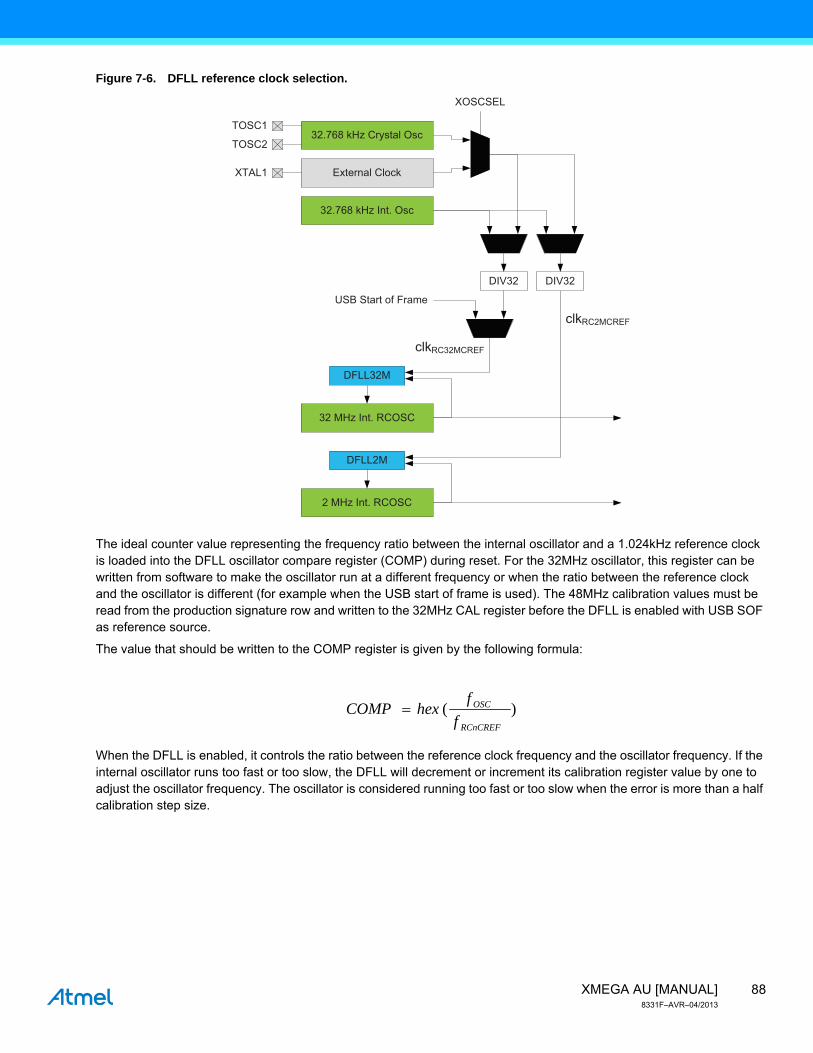
Figure 7-6. DFLL reference clock selection.
The ideal counter value representing the frequency ratio between the internal oscillator and a 1.024kHz reference clock is loaded into the DFLL oscillator compare register (COMP) during reset. For the 32MHz oscillator, this register can be written from software to make the oscillator run at a different frequency or when the ratio between the reference clock and the oscillator is different (for example when the USB start of frame is used). The 48MHz calibration values must be read from the production signature row and written to the 32MHz CAL register before the DFLL is enabled with USB SOF as reference source.
The value that should be written to the COMP register is given by the following formula:
When the DFLL is enabled, it controls the ratio between the reference clock frequency and the oscillator frequency. If the internal oscillator runs too fast or too slow, the DFLL will decrement or increment its calibration register value by one to adjust the oscillator frequency. The oscillator is considered running too fast or too slow when the error is more than a half calibration step size.
32.768 kHz Crystal Osc
External Clock
32.768 kHz Int. Osc
DFLL32M
32 MHz Int. RCOSC
DFLL2M
2 MHz Int. RCOSC
clkRC32MCREF
clkRC2MCREF
TOSC1
TOSC2
XTAL1
DIV32DIV32
XOSCSEL
USB Start of Frame
)(RCnCREF
OSC
f
fhexCOMP
89XMEGA AU [MANUAL]8331F–AVR–04/2013
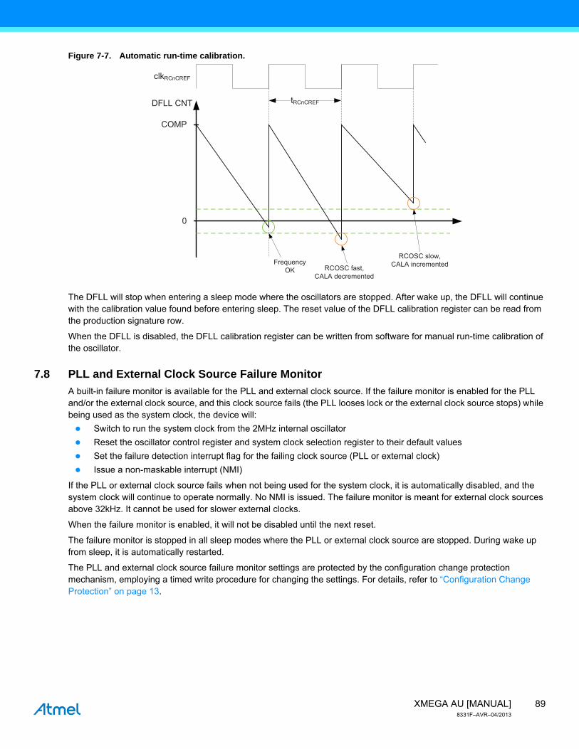
Figure 7-7. Automatic run-time calibration.
The DFLL will stop when entering a sleep mode where the oscillators are stopped. After wake up, the DFLL will continue with the calibration value found before entering sleep. The reset value of the DFLL calibration register can be read from the production signature row.
When the DFLL is disabled, the DFLL calibration register can be written from software for manual run-time calibration of the oscillator.
7.8 PLL and External Clock Source Failure Monitor
A built-in failure monitor is available for the PLL and external clock source. If the failure monitor is enabled for the PLL and/or the external clock source, and this clock source fails (the PLL looses lock or the external clock source stops) while being used as the system clock, the device will:
Switch to run the system clock from the 2MHz internal oscillator
Reset the oscillator control register and system clock selection register to their default values
Set the failure detection interrupt flag for the failing clock source (PLL or external clock)
Issue a non-maskable interrupt (NMI)
If the PLL or external clock source fails when not being used for the system clock, it is automatically disabled, and the system clock will continue to operate normally. No NMI is issued. The failure monitor is meant for external clock sources above 32kHz. It cannot be used for slower external clocks.
When the failure monitor is enabled, it will not be disabled until the next reset.
The failure monitor is stopped in all sleep modes where the PLL or external clock source are stopped. During wake up from sleep, it is automatically restarted.
The PLL and external clock source failure monitor settings are protected by the configuration change protection mechanism, employing a timed write procedure for changing the settings. For details, refer to “Configuration Change Protection” on page 13.
DFLL CNT
COMP
0
tRCnCREF
FrequencyOK RCOSC fast,
CALA decremented
RCOSC slow,CALA incremented
clkRCnCREF
90XMEGA AU [MANUAL]8331F–AVR–04/2013
7.9 Register Description – Clock
7.9.1 CTRL – Control register
Bit 7:3 – ReservedThese bits are unused and reserved for future use. For compatibility with future devices, always write these bits to zero when this register is written.
Bit 2:0 – SCLKSEL[2:0]: System Clock SelectionThese bits are used to select the source for the system clock. See Table 7-1 on page 90 for the different selec-tions. Changing the system clock source will take two clock cycles on the old clock source and two more clock cycles on the new clock source. These bits are protected by the configuration change protection mechanism. For details, refer to “Configuration Change Protection” on page 13.
SCLKSEL cannot be changed if the new clock source is not stable. The old clock can not be disabled until the clock switching is completed.
Table 7-1. System clock selection.
7.9.2 PSCTRL – Prescaler register
This register is protected by the configuration change protection mechanism. For details, refer to “Configuration Change Protection” on page 13.
Bit 7 – ReservedThis bit is unused and reserved for future use. For compatibility with future devices, always write this bit to zero when this register is written.
Bit 7 6 5 4 3 2 1 0
+0x00 – – – – – SCLKSEL[2:0]
Read/Write R R R R R R/W R/W R/W
Initial Value 0 0 0 0 0 0 0 0
SCLKSEL[2:0] Group configuration Description
000 RC2MHZ 2MHz internal oscillator
001 RC32MHZ 32MHz internal oscillator
010 RC32KHZ 32.768kHz internal oscillator
011 XOSC External oscillator or clock
100 PLL Phase locked loop
101 – Reserved
110 – Reserved
111 – Reserved
Bit 7 6 5 4 3 2 1 0
+0x01 – PSADIV[4:0] PSBCDIV
Read/Write R R/W R/W R/W R/W R/W R/W R/W
Initial Value 0 0 0 0 0 0 0 0
91XMEGA AU [MANUAL]8331F–AVR–04/2013
Bit 6:2 – PSADIV[4:0]: Prescaler A Division FactorThese bits define the division ratio of the clock prescaler A according to Table 7-2 on page 91. These bits can be written at run-time to change the frequency of the ClkPER4 clock relative to the system clock, ClkSYS.
Table 7-2. Prescaler A division factor.
Bit 1:0 – PSBCDIV: Prescaler B and C Division FactorsThese bits define the division ratio of the clock prescalers B and C according to Table 7-3 on page 91. Prescaler B will set the clock frequency for the ClkPER2 clock relative to the ClkPER4 clock. Prescaler C will set the clock fre-quency for the ClkPER and ClkCPU clocks relative to the ClkPER2 clock. Refer to Figure 7-5 on page 86 fore more details.
Table 7-3. Prescaler B and C division factors.
PSADIV[4:0] Group configuration Description
00000 1 No division
00001 2 Divide by 2
00011 4 Divide by 4
00101 8 Divide by 8
00111 16 Divide by 16
01001 32 Divide by 32
01011 64 Divide by 64
01101 128 Divide by 128
01111 256 Divide by 256
10001 512 Divide by 512
10101 Reserved
10111 Reserved
11001 Reserved
11011 Reserved
11101 Reserved
11111 Reserved
PSBCDIV[1:0] Group configuration Prescaler B division Prescaler C division
00 1_1 No division No division
01 1_2 No division Divide by 2
10 4_1 Divide by 4 No division
11 2_2 Divide by 2 Divide by 2
92XMEGA AU [MANUAL]8331F–AVR–04/2013
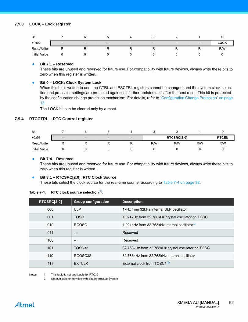
7.9.3 LOCK – Lock register
Bit 7:1 – ReservedThese bits are unused and reserved for future use. For compatibility with future devices, always write these bits to zero when this register is written.
Bit 0 – LOCK: Clock System LockWhen this bit is written to one, the CTRL and PSCTRL registers cannot be changed, and the system clock selec-tion and prescaler settings are protected against all further updates until after the next reset. This bit is protected by the configuration change protection mechanism. For details, refer to “Configuration Change Protection” on page 13.
The LOCK bit can be cleared only by a reset.
7.9.4 RTCCTRL – RTC Control register
Bit 7:4 – ReservedThese bits are unused and reserved for future use. For compatibility with future devices, always write these bits to zero when this register is written.
Bit 3:1 – RTCSRC[2:0]: RTC Clock SourceThese bits select the clock source for the real-time counter according to Table 7-4 on page 92.
Table 7-4. RTC clock source selection(1).
Notes: 1. This table is not applicable for RTC32
2. Not available on devices with Battery Backup System
Bit 7 6 5 4 3 2 1 0
+0x02 – – – – – – – LOCK
Read/Write R R R R R R R R/W
Initial Value 0 0 0 0 0 0 0 0
Bit 7 6 5 4 3 2 1 0
+0x03 – – – – RTCSRC[2:0] RTCEN
Read/Write R R R R R/W R/W R/W R/W
Initial Value 0 0 0 0 0 0 0 0
RTCSRC[2:0] Group configuration Description
000 ULP 1kHz from 32kHz internal ULP oscillator
001 TOSC 1.024kHz from 32.768kHz crystal oscillator on TOSC
010 RCOSC 1.024kHz from 32.768kHz internal oscillator(2)
011 – Reserved
100 – Reserved
101 TOSC32 32.768kHz from 32.768kHz crystal oscillator on TOSC
110 RCOSC32 32.768kHz from 32.768kHz internal oscillator
111 EXTCLK External clock from TOSC1(2)
93XMEGA AU [MANUAL]8331F–AVR–04/2013
Bit 0 – RTCEN: RTC Clock Source EnableSetting the RTCEN bit enables the selected RTC clock source for the real-time counter.
7.9.5 USBCTRL – USB Control register
Bit 7:6 – ReservedThese bits are unused and reserved for future use. For compatibility with future devices, always write these bits to zero when this register is written.
Bit 5:3 – USBPSDIV[2:0]: USB Prescaler Division FactorThese bits define the division ratio of the USB clock prescaler according to Table 7-5 on page 93. These bits are locked as long as the USB clock source is enabled.
Table 7-5. USB prescaler division factor.
Bit 2:1 – USBSRC[1:0]: USB Clock SourceThese bits select the clock source for the USB module according to Table 7-6 on page 93.
Table 7-6. USB clock source.
Note: 1. The 32MHz internal oscillator must be calibrated to 48MHz before selecting this as source for the USB device module. Refer to “DFLL 2MHz and DFLL 32MHz” on page 87.
Bit 0 – USBSEN: USB Clock Source EnableSetting this bit enables the selected clock source for the USB device module.
Bit 7 6 5 4 3 2 1 0
+0x04 – – USBPSDIV[2:0] USBSRC[1:0] USBSEN
Read/Write R R R/W R/W R/W R/W R/W R/W
Initial Value 0 0 0 0 0 0 0 0
USBPSDIV[2:0] Group configuration Description
000 1 No division
001 2 Divide by 2
010 4 Divide by 4
011 8 Divide by 8
100 16 Divide by 16
101 32 Divide by 32
110 – Reserved
111 – Reserved
USBSRC[1:0] Group configuration Description
00 PLL PLL
01 RC32M 32MHz internal oscillator(1)
94XMEGA AU [MANUAL]8331F–AVR–04/2013
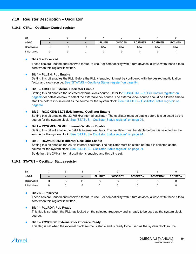
7.10 Register Description – Oscillator
7.10.1 CTRL – Oscillator Control register
Bit 7:5 – Reserved
These bits are unused and reserved for future use. For compatibility with future devices, always write these bits to zero when this register is written.
Bit 4 – PLLEN: PLL EnableSetting this bit enables the PLL. Before the PLL is enabled, it must be configured with the desired multiplication factor and clock source. See ”STATUS – Oscillator Status register” on page 94.
Bit 3 – XOSCEN: External Oscillator EnableSetting this bit enables the selected external clock source. Refer to “XOSCCTRL – XOSC Control register” on page 95 for details on how to select the external clock source. The external clock source should be allowed time to stabilize before it is selected as the source for the system clock. See ”STATUS – Oscillator Status register” on page 94.
Bit 2 – RC32KEN: 32.768kHz Internal Oscillator EnableSetting this bit enables the 32.768kHz internal oscillator. The oscillator must be stable before it is selected as the source for the system clock. See ”STATUS – Oscillator Status register” on page 94.
Bit 1 – RC32MEN: 32MHz Internal Oscillator EnableSetting this bit will enable the 32MHz internal oscillator. The oscillator must be stable before it is selected as the source for the system clock. See ”STATUS – Oscillator Status register” on page 94.
Bit 0 – RC2MEN: 2MHz Internal Oscillator EnableSetting this bit enables the 2MHz internal oscillator. The oscillator must be stable before it is selected as the source for the system clock. See ”STATUS – Oscillator Status register” on page 94.
By default, the 2MHz internal oscillator is enabled and this bit is set.
7.10.2 STATUS – Oscillator Status register
Bit 7:5 – ReservedThese bits are unused and reserved for future use. For compatibility with future devices, always write these bits to zero when this register is written.
Bit 4 – PLLRDY: PLL ReadyThis flag is set when the PLL has locked on the selected frequency and is ready to be used as the system clock source.
Bit 3 – XOSCRDY: External Clock Source ReadyThis flag is set when the external clock source is stable and is ready to be used as the system clock source.
Bit 7 6 5 4 3 2 1 0
+0x00 – – – PLLEN XOSCEN RC32KEN RC32MEN RC2MEN
Read/Write R R R R/W R/W R/W R/W R/W
Initial Value 0 0 0 0 0 0 0 1
Bit 7 6 5 4 3 2 1 0
+0x01 – – – PLLRDY XOSCRDY RC32KRDY RC32MRDY RC2MRDY
Read/Write R R R R R R R R
Initial Value 0 0 0 0 0 0 0 0
95XMEGA AU [MANUAL]8331F–AVR–04/2013
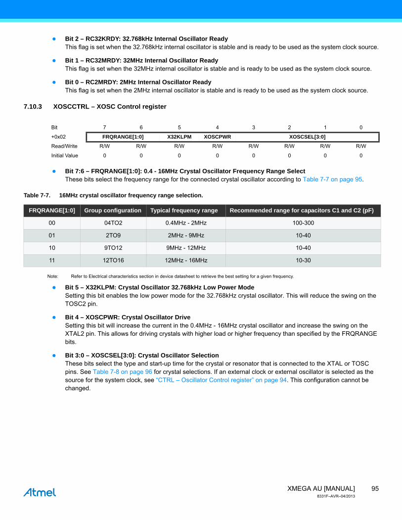
Bit 2 – RC32KRDY: 32.768kHz Internal Oscillator ReadyThis flag is set when the 32.768kHz internal oscillator is stable and is ready to be used as the system clock source.
Bit 1 – RC32MRDY: 32MHz Internal Oscillator ReadyThis flag is set when the 32MHz internal oscillator is stable and is ready to be used as the system clock source.
Bit 0 – RC2MRDY: 2MHz Internal Oscillator ReadyThis flag is set when the 2MHz internal oscillator is stable and is ready to be used as the system clock source.
7.10.3 XOSCCTRL – XOSC Control register
Bit 7:6 – FRQRANGE[1:0]: 0.4 - 16MHz Crystal Oscillator Frequency Range SelectThese bits select the frequency range for the connected crystal oscillator according to Table 7-7 on page 95.
Table 7-7. 16MHz crystal oscillator frequency range selection.
Note: Refer to Electrical characteristics section in device datasheet to retrieve the best setting for a given frequency.
Bit 5 – X32KLPM: Crystal Oscillator 32.768kHz Low Power ModeSetting this bit enables the low power mode for the 32.768kHz crystal oscillator. This will reduce the swing on the TOSC2 pin.
Bit 4 – XOSCPWR: Crystal Oscillator DriveSetting this bit will increase the current in the 0.4MHz - 16MHz crystal oscillator and increase the swing on the XTAL2 pin. This allows for driving crystals with higher load or higher frequency than specified by the FRQRANGE bits.
Bit 3:0 – XOSCSEL[3:0]: Crystal Oscillator SelectionThese bits select the type and start-up time for the crystal or resonator that is connected to the XTAL or TOSC pins. See Table 7-8 on page 96 for crystal selections. If an external clock or external oscillator is selected as the source for the system clock, see “CTRL – Oscillator Control register” on page 94. This configuration cannot be changed.
Bit 7 6 5 4 3 2 1 0
+0x02 FRQRANGE[1:0] X32KLPM XOSCPWR XOSCSEL[3:0]
Read/Write R/W R/W R/W R/W R/W R/W R/W R/W
Initial Value 0 0 0 0 0 0 0 0
FRQRANGE[1:0] Group configuration Typical frequency range Recommended range for capacitors C1 and C2 (pF)
00 04TO2 0.4MHz - 2MHz 100-300
01 2TO9 2MHz - 9MHz 10-40
10 9TO12 9MHz - 12MHz 10-40
11 12TO16 12MHz - 16MHz 10-30
96XMEGA AU [MANUAL]8331F–AVR–04/2013
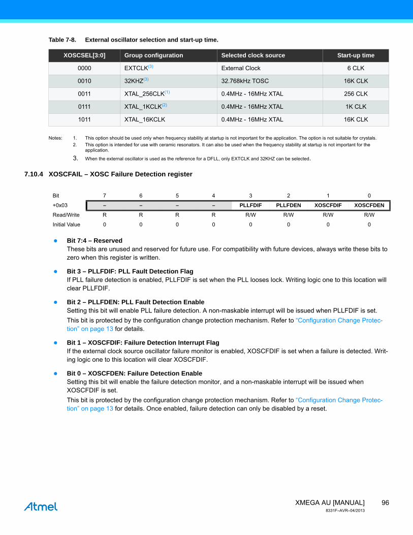
Table 7-8. External oscillator selection and start-up time.
Notes: 1. This option should be used only when frequency stability at startup is not important for the application. The option is not suitable for crystals.
2. This option is intended for use with ceramic resonators. It can also be used when the frequency stability at startup is not important for the application.
3. When the external oscillator is used as the reference for a DFLL, only EXTCLK and 32KHZ can be selected.
7.10.4 XOSCFAIL – XOSC Failure Detection register
Bit 7:4 – ReservedThese bits are unused and reserved for future use. For compatibility with future devices, always write these bits to zero when this register is written.
Bit 3 – PLLFDIF: PLL Fault Detection FlagIf PLL failure detection is enabled, PLLFDIF is set when the PLL looses lock. Writing logic one to this location will clear PLLFDIF.
Bit 2 – PLLFDEN: PLL Fault Detection EnableSetting this bit will enable PLL failure detection. A non-maskable interrupt will be issued when PLLFDIF is set.
This bit is protected by the configuration change protection mechanism. Refer to “Configuration Change Protec-tion” on page 13 for details.
Bit 1 – XOSCFDIF: Failure Detection Interrupt FlagIf the external clock source oscillator failure monitor is enabled, XOSCFDIF is set when a failure is detected. Writ-ing logic one to this location will clear XOSCFDIF.
Bit 0 – XOSCFDEN: Failure Detection EnableSetting this bit will enable the failure detection monitor, and a non-maskable interrupt will be issued when XOSCFDIF is set.
This bit is protected by the configuration change protection mechanism. Refer to “Configuration Change Protec-tion” on page 13 for details. Once enabled, failure detection can only be disabled by a reset.
XOSCSEL[3:0] Group configuration Selected clock source Start-up time
0000 EXTCLK(3) External Clock 6 CLK
0010 32KHZ(3) 32.768kHz TOSC 16K CLK
0011 XTAL_256CLK(1) 0.4MHz - 16MHz XTAL 256 CLK
0111 XTAL_1KCLK(2) 0.4MHz - 16MHz XTAL 1K CLK
1011 XTAL_16KCLK 0.4MHz - 16MHz XTAL 16K CLK
Bit 7 6 5 4 3 2 1 0
+0x03 – – – – PLLFDIF PLLFDEN XOSCFDIF XOSCFDEN
Read/Write R R R R R/W R/W R/W R/W
Initial Value 0 0 0 0 0 0 0 0
97XMEGA AU [MANUAL]8331F–AVR–04/2013
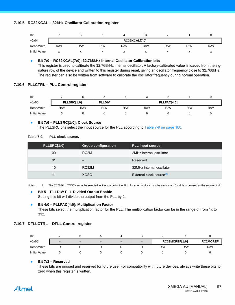
7.10.5 RC32KCAL – 32kHz Oscillator Calibration register
Bit 7:0 – RC32KCAL[7:0]: 32.768kHz Internal Oscillator Calibration bitsThis register is used to calibrate the 32.768kHz internal oscillator. A factory-calibrated value is loaded from the sig-nature row of the device and written to this register during reset, giving an oscillator frequency close to 32.768kHz. The register can also be written from software to calibrate the oscillator frequency during normal operation.
7.10.6 PLLCTRL – PLL Control register
Bit 7:6 – PLLSRC[1:0]: Clock SourceThe PLLSRC bits select the input source for the PLL according to Table 7-9 on page 100.
Table 7-9. PLL clock source.
Notes: 1. The 32.768kHz TOSC cannot be selected as the source for the PLL. An external clock must be a minimum 0.4MHz to be used as the source clock.
Bit 5 – PLLDIV: PLL Divided Output EnableSetting this bit will divide the output from the PLL by 2.
Bit 4:0 – PLLFAC[4:0]: Multiplication FactorThese bits select the multiplication factor for the PLL. The multiplication factor can be in the range of from 1x to 31x.
7.10.7 DFLLCTRL – DFLL Control register
Bit 7:3 – ReservedThese bits are unused and reserved for future use. For compatibility with future devices, always write these bits to zero when this register is written.
Bit 7 6 5 4 3 2 1 0
+0x04 RC32KCAL[7:0]
Read/Write R/W R/W R/W R/W R/W R/W R/W R/W
Initial Value x x x x x x x x
Bit 7 6 5 4 3 2 1 0
+0x05 PLLSRC[1:0] PLLDIV PLLFAC[4:0]
Read/Write R/W R/W R/W R/W R/W R/W R/W R/W
Initial Value 0 0 0 0 0 0 0 0
PLLSRC[1:0] Group configuration PLL input source
00 RC2M 2MHz internal oscillator
01 – Reserved
10 RC32M 32MHz internal oscillator
11 XOSC External clock source(1)
Bit 7 6 5 4 3 2 1 0
+0x06 – – – – – RC32MCREF[1:0] RC2MCREF
Read/Write R R R R R R/W R/W R/W
Initial Value 0 0 0 0 0 0 0 0
98XMEGA AU [MANUAL]8331F–AVR–04/2013
Bit 2:1 – RC32MCREF[1:0]: 32MHz Oscillator Calibration ReferenceThese bits are used to select the calibration source for the 32MHz DFLL according to the Table 7-10 on page 101. These bits will select only which calibration source to use for the DFLL. In addition, the actual clock source that is selected must enabled and configured for the calibration to function.
Table 7-10. 32MHz oscillator reference selection.
Bit 0 – RC2MCREF: 2MHz Oscillator Calibration ReferenceThis bit is used to select the calibration source for the 2MHz DFLL. By default, this bit is zero and the 32.768kHz internal oscillator is selected. If this bit is set to one, the 32.768kHz crystal oscillator on TOSC is selected as the reference. This bit will select only which calibration source to use for the DFLL. In addition, the actual clock source that is selected must enabled and configured for the calibration to function.
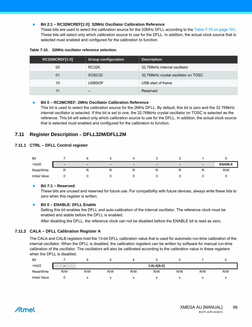
7.11 Register Description – DFLL32M/DFLL2M
7.11.1 CTRL – DFLL Control register
Bit 7:1 – ReservedThese bits are unused and reserved for future use. For compatibility with future devices, always write these bits to zero when this register is written.
Bit 0 – ENABLE: DFLL EnableSetting this bit enables the DFLL and auto-calibration of the internal oscillator. The reference clock must be enabled and stable before the DFLL is enabled.
After disabling the DFLL, the reference clock can not be disabled before the ENABLE bit is read as zero.
7.11.2 CALA – DFLL Calibration Register A
The CALA and CALB registers hold the 13-bit DFLL calibration value that is used for automatic run-time calibration of the internal oscillator. When the DFLL is disabled, the calibration registers can be written by software for manual run-time calibration of the oscillator. The oscillators will also be calibrated according to the calibration value in these registers when the DFLL is disabled.
RC32MCREF[1:0] Group configuration Description
00 RC32K 32.768kHz internal oscillator
01 XOSC32 32.768kHz crystal oscillator on TOSC
10 USBSOF USB start of frame
11 – Reserved
Bit 7 6 5 4 3 2 1 0
+0x00 – – – – – – – ENABLE
Read/Write R R R R R R R R/W
Initial Value 0 0 0 0 0 0 0 0
Bit 7 6 5 4 3 2 1 0
+0x02 – CALA[6:0]
Read/Write R/W R/W R/W R/W R/W R/W R/W R/W
Initial Value 0 x x x x x x x
99XMEGA AU [MANUAL]8331F–AVR–04/2013
Bit 7 – ReservedThis bit is unused and reserved for future use. For compatibility with future devices, always write this bit to zero when this register is written.
Bit 6:0 – CALA[6:0]: DFLL Calibration BitsThese bits hold the part of the oscillator calibration value that is used for automatic runtime calibration. A factory-calibrated value is loaded from the signature row of the device and written to this register during reset, giving an oscillator frequency approximate to the nominal frequency for the oscillator. The bits cannot be written when the DFLL is enabled.
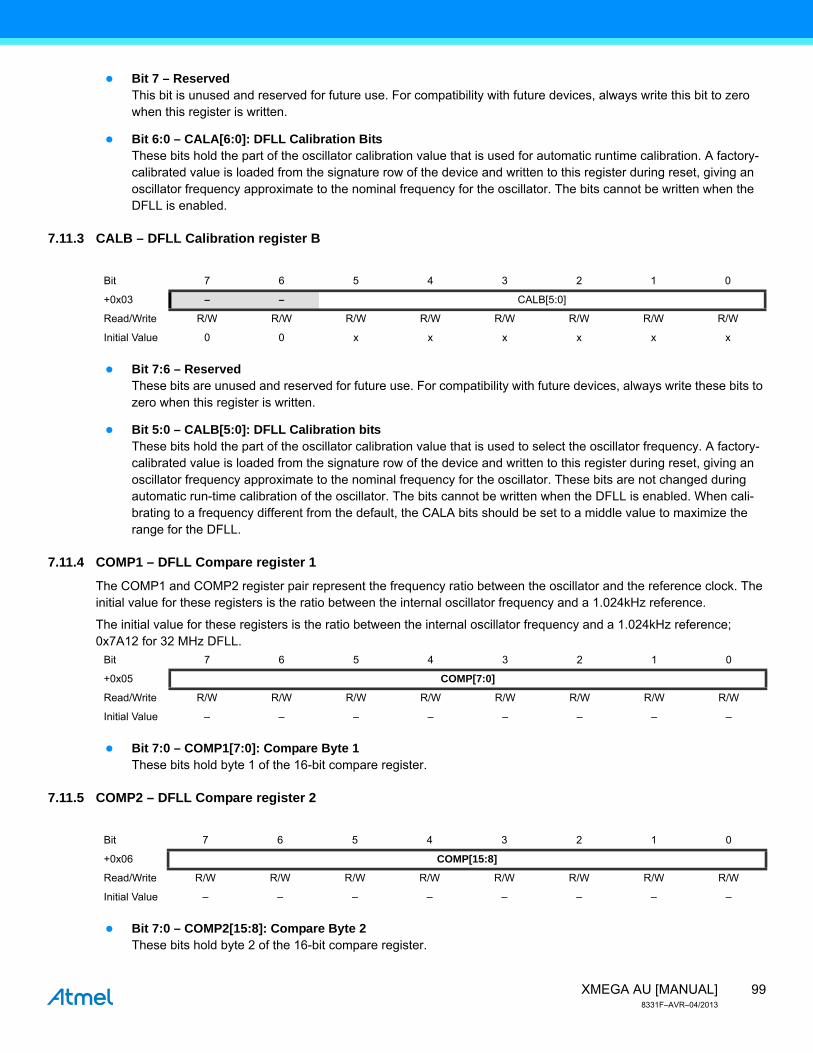
7.11.3 CALB – DFLL Calibration register B
Bit 7:6 – ReservedThese bits are unused and reserved for future use. For compatibility with future devices, always write these bits to zero when this register is written.
Bit 5:0 – CALB[5:0]: DFLL Calibration bitsThese bits hold the part of the oscillator calibration value that is used to select the oscillator frequency. A factory-calibrated value is loaded from the signature row of the device and written to this register during reset, giving an oscillator frequency approximate to the nominal frequency for the oscillator. These bits are not changed during automatic run-time calibration of the oscillator. The bits cannot be written when the DFLL is enabled. When cali-brating to a frequency different from the default, the CALA bits should be set to a middle value to maximize the range for the DFLL.
7.11.4 COMP1 – DFLL Compare register 1
The COMP1 and COMP2 register pair represent the frequency ratio between the oscillator and the reference clock. The initial value for these registers is the ratio between the internal oscillator frequency and a 1.024kHz reference.
The initial value for these registers is the ratio between the internal oscillator frequency and a 1.024kHz reference; 0x7A12 for 32 MHz DFLL.
Bit 7:0 – COMP1[7:0]: Compare Byte 1These bits hold byte 1 of the 16-bit compare register.
7.11.5 COMP2 – DFLL Compare register 2
Bit 7:0 – COMP2[15:8]: Compare Byte 2These bits hold byte 2 of the 16-bit compare register.
Bit 7 6 5 4 3 2 1 0
+0x03 – – CALB[5:0]
Read/Write R/W R/W R/W R/W R/W R/W R/W R/W
Initial Value 0 0 x x x x x x
Bit 7 6 5 4 3 2 1 0
+0x05 COMP[7:0]
Read/Write R/W R/W R/W R/W R/W R/W R/W R/W
Initial Value – – – – – – – –
Bit 7 6 5 4 3 2 1 0
+0x06 COMP[15:8]
Read/Write R/W R/W R/W R/W R/W R/W R/W R/W
Initial Value – – – – – – – –
100XMEGA AU [MANUAL]8331F–AVR–04/2013
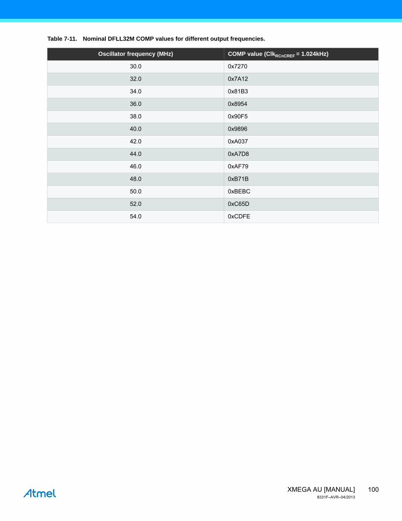
Table 7-11. Nominal DFLL32M COMP values for different output frequencies.
Oscillator frequency (MHz) COMP value (ClkRCnCREF = 1.024kHz)
30.0 0x7270
32.0 0x7A12
34.0 0x81B3
36.0 0x8954
38.0 0x90F5
40.0 0x9896
42.0 0xA037
44.0 0xA7D8
46.0 0xAF79
48.0 0xB71B
50.0 0xBEBC
52.0 0xC65D
54.0 0xCDFE
101XMEGA AU [MANUAL]8331F–AVR–04/2013
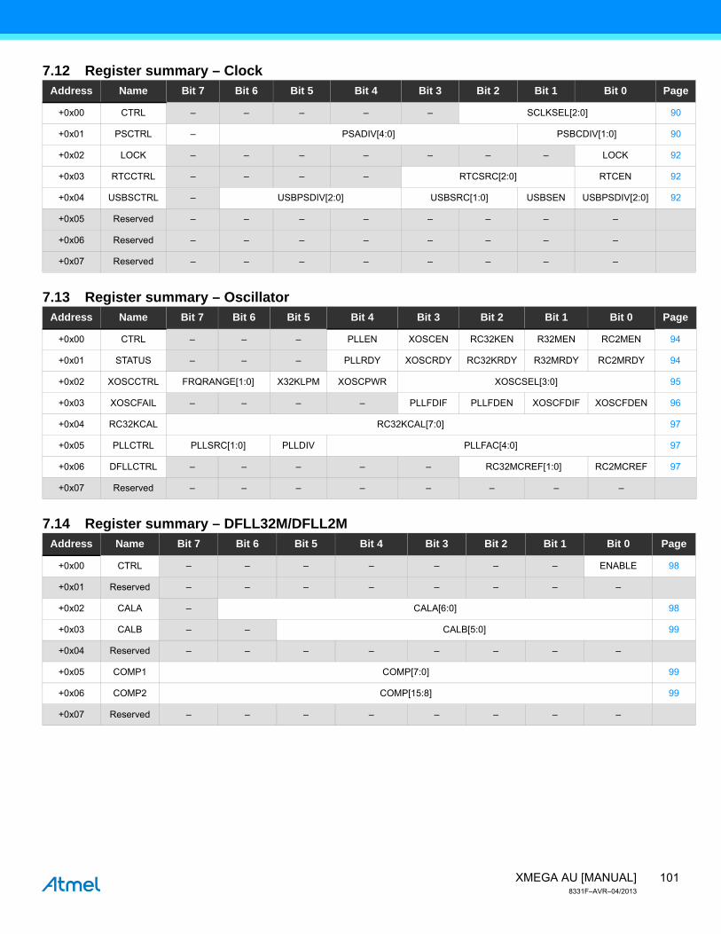
7.12 Register summary – Clock
7.13 Register summary – Oscillator
7.14 Register summary – DFLL32M/DFLL2M
Address Name Bit 7 Bit 6 Bit 5 Bit 4 Bit 3 Bit 2 Bit 1 Bit 0 Page
+0x00 CTRL – – – – – SCLKSEL[2:0] 90
+0x01 PSCTRL – PSADIV[4:0] PSBCDIV[1:0] 90
+0x02 LOCK – – – – – – – LOCK 92
+0x03 RTCCTRL – – – – RTCSRC[2:0] RTCEN 92
+0x04 USBSCTRL – USBPSDIV[2:0] USBSRC[1:0] USBSEN USBPSDIV[2:0] 92
+0x05 Reserved – – – – – – – –
+0x06 Reserved – – – – – – – –
+0x07 Reserved – – – – – – – –
Address Name Bit 7 Bit 6 Bit 5 Bit 4 Bit 3 Bit 2 Bit 1 Bit 0 Page
+0x00 CTRL – – – PLLEN XOSCEN RC32KEN R32MEN RC2MEN 94
+0x01 STATUS – – – PLLRDY XOSCRDY RC32KRDY R32MRDY RC2MRDY 94
+0x02 XOSCCTRL FRQRANGE[1:0] X32KLPM XOSCPWR XOSCSEL[3:0] 95
+0x03 XOSCFAIL – – – – PLLFDIF PLLFDEN XOSCFDIF XOSCFDEN 96
+0x04 RC32KCAL RC32KCAL[7:0] 97
+0x05 PLLCTRL PLLSRC[1:0] PLLDIV PLLFAC[4:0] 97
+0x06 DFLLCTRL – – – – – RC32MCREF[1:0] RC2MCREF 97
+0x07 Reserved – – – – – – – –
Address Name Bit 7 Bit 6 Bit 5 Bit 4 Bit 3 Bit 2 Bit 1 Bit 0 Page
+0x00 CTRL – – – – – – – ENABLE 98
+0x01 Reserved – – – – – – – –
+0x02 CALA – CALA[6:0] 98
+0x03 CALB – – CALB[5:0] 99
+0x04 Reserved – – – – – – – –
+0x05 COMP1 COMP[7:0] 99
+0x06 COMP2 COMP[15:8] 99
+0x07 Reserved – – – – – – – –
102XMEGA AU [MANUAL]8331F–AVR–04/2013
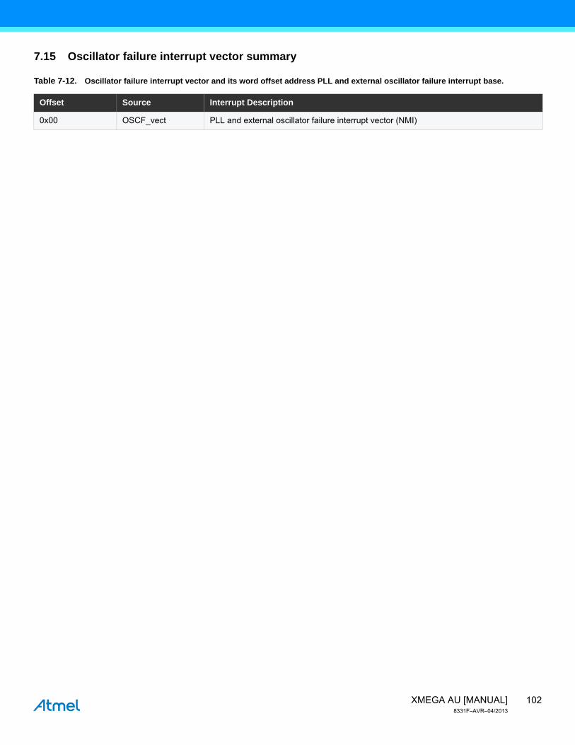
7.15 Oscillator failure interrupt vector summary
Table 7-12. Oscillator failure interrupt vector and its word offset address PLL and external oscillator failure interrupt base.
Offset Source Interrupt Description
0x00 OSCF_vect PLL and external oscillator failure interrupt vector (NMI)