:7 :--- MICAD Macros Make =: Circuit Layout Easy WAVEGUIDE EEsoF MICAD MACROS MAKE CIRCUIT LAYOUT...
50
r NASA Technical Memorandum 103272 //F--3 /C7,, = :7 :--- Coplanar WaVeguide EEsoF .......... MICAD Macros Make =:_ ...... Circuit Layout Easy George E, Poncliak _ Lewis Research Center ...... Cleveland, Ohio and Nikola Visic .............. Cleveland State University Cleveland, Ohio September 1990 : ..... NICAD •::<_ ':_ --- (NASA) (NA_A-TM-103272) COPLANAR WAVEGUIOE EEsoF Ngl-lO33Z MACROS MAKE CIkCOIT LAYOUT EASY :..... ,= 39 p CSCL 09C Unclas G3/32 0001671 --,_rl • https://ntrs.nasa.gov/search.jsp?R=19910010019 2018-06-26T11:12:16+00:00Z
Transcript of :7 :--- MICAD Macros Make =: Circuit Layout Easy WAVEGUIDE EEsoF MICAD MACROS MAKE CIRCUIT LAYOUT...

r
NASA Technical Memorandum 103272
//F--3
/C7,,=
:7 :--- Coplanar WaVeguide EEsoF.......... MICAD Macros Make
=:_ ......Circuit Layout Easy
George E, Poncliak _Lewis Research Center ......
Cleveland, Ohio
and
Nikola Visic ..............
Cleveland State UniversityCleveland, Ohio
September 1990 : .....
NICAD
•::<_ ':_ --- (NASA)
(NA_A-TM-103272) COPLANAR WAVEGUIOE EEsoF Ngl-lO33ZMACROS MAKE CIkCOIT LAYOUT EASY :.....
,=
39 p CSCL 09C
Unclas
G3/32 0001671--,_rl •
https://ntrs.nasa.gov/search.jsp?R=19910010019 2018-06-26T11:12:16+00:00Z


INDEX FOR
MICAD MACRO FILES
CBEND
CCORN
CCP
CCPLR
CCURVE
CGAP
COPEN
CSHORT
CSPURC
CSPURG
CSTART
CSTARTP
CSTEP
CSTUBC
CSTUBG
CSTUBO
CSTUBS
CTAPER
CTEEI
CTEE2
Bend
Corner
Connection Point
Interdigital Coupler
Curve
Gap
Open Circuit
Short Circuit
Spurline Filterin the Center Conductor
Spurline Filterin the Ground Plane
Open at Input
Open at Input with Padsfor RF Wafer Probes
Step
Slot Stub
in the Center Conductor
Slot Stub
in the Ground Plane
Open Ended Stub
Short Circuit Terminated Stub
Taper
T Junction
T Junction
5
7
9
ii
13
15
17
19
21
23
25
27
29
31
33
35
37
39
41
43

COPLANAR WAVEGUIDE EEsoF MICAD MACROS MAKE CIRCUIT LAYOUT EASY
George E. Ponchak
National Aeronautics and Space AdministrationLewis Research Center
Cleveland, Ohio 44135
and
Nikola Visic*
Cleveland State University
Cleveland, Ohio 44115
_4
l
AB STRAC T
A collection of macro files is presented which permit the
layout of coplanar waveguide integrated circuits using EEsoFMICAD CAD software. The files must be added to the usersMICAD.ELE file.
INTRODUCTION
Coplanar waveguide (CPW) is a transmission line with a
center strip conductor and a semi-infinite ground plane on either
side [I]. Grounded coplanar waveguide (GCPW) has an additionalground plane on the back side of the substrate. Both of these
transmission lines are highly suitable for low cost integrated
circuit fabrication since the center conductor and the ground
plane are on the same side of the substrate. This permits easyshunt as well as series connection of circuit elements without
the need for wafer thinning and via hole fabrication. The
difficulty with using CPW for integrated circuits has been the
lack of circuit models and CAD layout tools.
EEsoF MICAD software is a CAD system for the layout and mask
generation of etched microwave circuits. If the microwave circuit
is to be fabricated by liftoff techniques or selective metal
buildup as done in electroplating, then the negative of the
generated mask must be used. Within MICAD, there is the ability
to create templates to describe the CPW circuit elements. This is
accomplished by creating macro files and appending them to theMICAD.ELE file [2]. The macro files are codes which describe the
circuit element on a cartesian coordinate system. A series of
macro files have been created to layout CPW elements. A diagram
of the element, an example of how to incorporate the element into
a EEsoF circuit file, and the macro file are presented in theformat of the EEsoF element catalog in the EEsoF manuals. This
should permit the addition of these macros into the users manual
for easy use.
USE OF MICAD MACROS
The coplanar waveguide macros have been designed to work on
plotting tables so that rubylith masks can be made. Not all of
_Co-op Student at NASA Lewis Research Center.
the macros will work with other mask making systems. This isbecause coplanar waveguide has semi-infinite ground planes which
are not closed surfaces. Therefore, the ground planes are defined
as open surfaces. The circuit boundaries must be drawn by theuser after the drawing is generated by Micad. In addition, Micad
demands that the circuit nodes be defined on closed polygon
surfaces. Although this is not a problem with other transmission
line structures, this causes a problem with some CPW circuits
which terminate the center conductor onto the ground planes whichare defined as open surfaces• For these structures, the short
circuit and short circuit terminated stub for example, anunwanted line will be plotted or cut into the rubylith. If care
is taken not to peel the rubylith at this cut mark and a mask
reduction is performed, the unwanted cut will not adverselyeffect the final mask.
The Micad macros may be typed into the MICAD.ELE file using
the MICAD text editor or a word processor with an ASCII save
feature. Although not stated in the MICAD manuals, there appearsto be a size limit to the MICAD.ELE file length which can be read
into the MICAD program. Therefore, it may be necessary to comment
out the macro files in the MICAD.ELE file not required for the
circuit being drawn• After the macros have been appended to theMICAD.ELE file, they may be used the same as "elements" are to
layout a mask. An example of this is shown in Figures 1 and 2.
Figure 1 is the EEsoF circuit file for a typical CPW 1 to 4 power
divider with DC blocking capacitors and connection points for
MMIC's. Figure 2 is the drawing for this circuit.
CONCLUSIONS
MICAD macro programs have been written which permit the
layout of CPW circuits. These macros may be used with theelements supplied by EEsoF to create complex masks on a plottingmachine.
•
REFERENCES
Wen, C.P.,"Coplanar Waveguide: A Surface Strip Transmission
Line Suitable for Nonreciprocal Gyromagnetic Applications,"
IEEE Trans. Microwave Theory Tech., vol. MTT-17, no. 12,
Dec. 1969, pp. 1087-1090.
2. EEsoF Micad Reference Manual.
2

dimfreq ghzres ohind nhcap pfing miltime pscond /oh
ang degckt
cpw 1 2 w=12 g=lO 1=214.5cstubo 2 3 w=12 g=12 osl=lO os2=12 os3=12 os4=20
cpw 3 4 w=12 g=lO 1=150
ctaper 4 5 wl=12 gl=lO w2=40 g2=10 It=i03.5
cpw 5 6 w=40 g=lO 1=50
ccplr 7 6 w=40 g=lO scl=5 sc2=5 sc3=5 sc4=lO sc5=82.6
cpw 7 8 w=40 g=lO 1=50
ctaper 8 9 wl=40 gl=lO w2=lO g2=10 it=150
ccp 9 i0 wl=lO gl=lO 11=5 d=lO0 w2=lO g2=lO 12=5
ctaper i0 ii wl=lO gl=lO w2=40 g2=10 It=150
cpw ii 12 w=40 g=lO 1=50
ccplr 12 13 w=40 g=lO scl=5 sc2=5 sc3=5 sc4=10 sc5=82.6
cpw 13 14 w=40 g=lO 1=50
ctaper 14 15 wl=40 gl=lO w2=12 g2=10 it=100
cpw 15 16 w=12 g=lO I=i00
def2p 1 16 armctaper 1 2 wl=12 gl=lO w2=60 g2=10 It=103.5
cteel 2 3 4 wi=60 gl=lO w2=12 g2=10 w3=12 g3=10
cpw 3 5 w=12 g=lO 1=141.5
ccorn 5 6 w=12 g=lO
cpw 4 7 w=12 g=lO 1=141.5
ccorn 8 7 w=12 g=lO
def3p 1 6 8 branchctaper 1 2 wl=12 gl=lO w2=60 g2=10 It=240
cteel 2 3 9 wl=60 gl=lO w2=12 g2=lO w3=12 g3=10
cpw 3 4 w=12 g=lO 1=150cstubg 4 5 w=12 g=lO zgl=29 zg2=lO
cpw 5 6 w=12 g=lO 1=150ccorn 6 7 w=12 g=lO
cpw 7 8 w=12 g=lO 1=114.5
cpw 9 ii w=12 g=lO 1=150
cstubg ii 12 w=12 g=lO zgl=29 zg2=lO
cpw 12 13 w=12 g=lO 1=150
ccorn 14 13 w=12 g=lO
cpw 14 15 w=12 g=lO 1=114.5branch 8 50 51
branch 15 52 53
arm 50 54
arm 51 55
arm 52 56
arm 53 57
def5p 1 54 55 56 57 print
Figu_ 1. MICAD cir_it file _r a CPW 1 _ 4 p_er di_der.

_ CTEE 1
. I'-L_
z._CSTUBO /-- CCPLR v_ CCP
L. MMIC
CCORN
Figure 2. CPW ! {o 4 ower divider,

CBEND Coplanar Waveguide Bend CBEND
Physical layout:
G
W nl,
G
Data:
W=Strip width
G=Slot width
ANG=Angle of bend
_""_ANG
Syntax:
CBEND nl n2 W=xl G=x2 ANG=x3
Example:
CBEND 1 2 W=25 G=I0 ANG=40
Notes:
I. This is a macro program in the MICAD.ELE file.
2. The program is valid for 0<=ANG<=I80 degree.
5
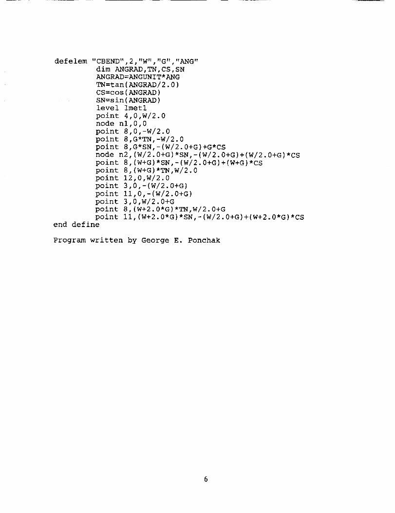
defelem
end
"CBEND",2,"W","G","ANG"
dim ANGRAD,TN,CS,SNANGRAD=ANGUNIT*ANG
TN=tan(ANGRAD/2.0)
CS=cos(ANGRAD)
SN=sin(ANGRAD)level Imetl
point 4,0,W/2.0
node nl,
point 8,
point 8,
point 8,node n2,
point 8,point
point
point
point
pointpoint
pointdefine
0,0
0,-W/2.0
G*TN,-W/2.0
G*SN,-(W/2.0+G)+G*CS
(W/2.0+G)*SN,-(W/2.0+G)+(W/2.0+G)*CS
(W+G)*SN,-(W/2.0+G)+(W+G)*CS
8,(W+G)*TN,W/2.012,0,W/2.0
3,0,-(W/2.0+G)
II,0,-(W/2.0+G)
3,0,W/2.0+G
8,(W+2.0*G)*TN,W/2.0+G
II,(W+2.0*G)*SN,-(W/2.0+G)+(W+2.0*G)*CS
Program written by George E. Ponchak
6
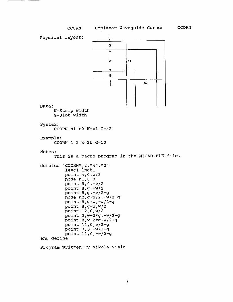
CCORN Coplanar Waveguide Corner CCORN
Physical layout:
Data:
W=Strip widthG=Slot width
G
Tw
G
,I
.2
Syntax:
CCORN nl n2 W=xl G=x2
Example:CCORN 1 2 W=25 G=I0
Notes:
This is a macro program in the MICAD.ELE file.
defelem "CCORN",2,"W","G"
level imetl
point 4,0,w/2
node nl,0,0
point 8,0,-w/2
point 8,g,-w/2
point 8,g,-w/2-g
node n2,g+w/2,-w/2-g
point 8,g+w,-w/2-g
point 8,g+w,w/2
polnt 12,0,w/2
point 3,w+2*g,-w/2-g
point 8,w+2*g,w/2+g
point ll,0,w/2+g
point 3,0,-w/2-g
point ll,0,-w/2-gend define
Program written by Nikola Visic

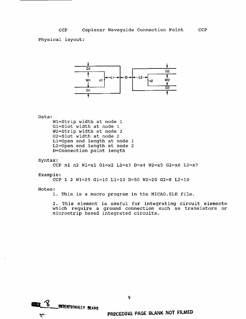
CCP Coplanar Waveguide Connection Point
Physical layout:
CCP
GI
tw1
GI
G2
n2 W2
G2
Data:
Wl=Strip width at node 1Gl=Slot width at node 1
W2=Strip width at node 2G2=Slot width at node 2
Ll=Open end length at node 1
L2=Open end length at node 2
D=Connection point length
Syntax:CCP nl n2 Wl=xl Gl=x2 Ll=x3 D=x4 W2=x5 G2=x6 L2=x7
Example:
CCP 1 2 WI=25 GI=I0 LI=I0 D=50 W2=20 G2=8 L2=I0
Notes:
i. This is a macro program in the MICAD.ELE file.
2. This element is useful for integrating circuit elements
which require a ground connection such as transistors or
microstrip based integrated circuits.
• "L _
9
PRL: CEDir4GPAGE BLANK NOT FILMED
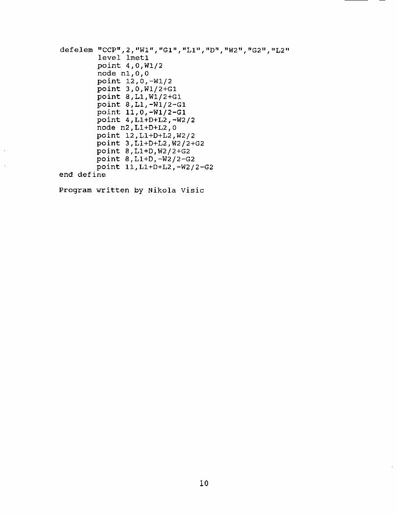
defelem
end
"CCP",2,"WI","GI","LI","D","W2","G2","L2"level imetl
point 4,0,WI/2
node nl,0,0
point 12,0,-Wi/2
point 3,0,WI/2+GI
point 8,LI,WI/2+GI
point 8,LI,-WI/2-GI
point II,0,-WI/2-GI
point 4,LI+D+L2,-W2/2
node n2,LI+D+L2,0
point
point
point
point
pointdefine
12,LI+D+L2,W2/2
3,LI+D+L2,W2/2+G2
8,LI+D,W2/2+G2
8,LI+D,-W2/2-G2
II,LI+D+L2,-W2/2-G2
Program written by Nikola Visic
i0

CCPLR Coplanar Waveguide Interdigital Coupler
Physical layout:
CCPLR
Data:
Tw
SC1 _-
-1, i,G
i
W=Strip width
G=Slot width
SCl=Slot width
SC2=Slot width
SC3=Slot width
SC4=Center conductor width in the coupler region
SC5=Length of the center conductor in the coupler region
Syntax:
CCPLR nl n2 W=xl G=x2 SCI=x3 SC2=x4 SC3=x5 SC4=x6 SC5=x7
Example:
CCPLR 1 2 W=25 G=I0 SCI=I0 SC2=5 SC3=5 SC4=8 SC5=50
Notes:
i. This is a macro program in the MICAD.ELE file.
2. The program does not run a check on the validity of the
data. It is up to the user to check that 2.SC2+SC4<W.
Ii
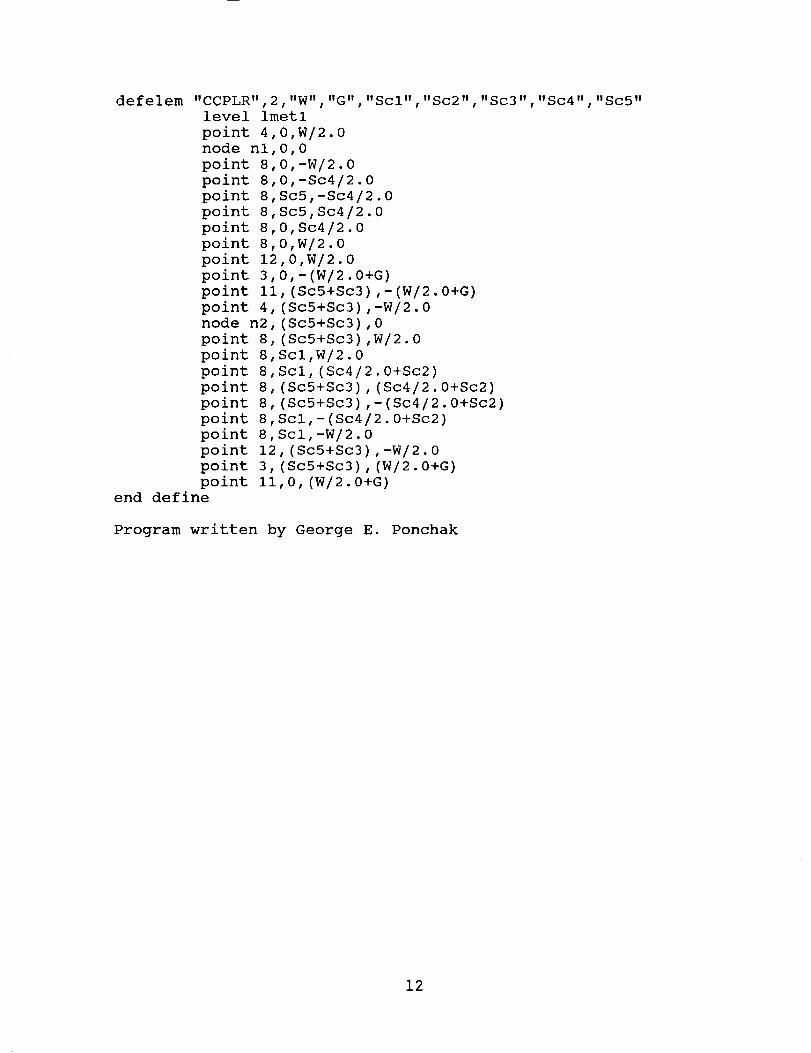
defelem "CCPLR",2,"W","G","ScI","Sc2","Sc3","Sc4"
level imetl
point 4,0,W/2.0
node nl,O,0
point 8,0,-W/2.0
point 8,0,-Sc4/2.0
point 8,Sc5,-Sc4/2.0
point 8,Sc5,Sc4/2.0
point 8,0,Sc4/2.0
point 8,0,W/2.0
point 12,0,W/2.0
point 3,0,-(W/2.0+G)
point ii, (Sc5+Sc3),-(W/2.0+G)
point 4, (Sc5+Sc3),-W/2.0
node n2, (Sc5+Sc3) ,0
point 8, (Sc5+Sc3),W/2.0
point 8,Sci,W/2.0
point 8,Scl, (Sc4/2.0+Sc2)
point 8, (Sc5+Sc3), (Sc4/2.0+Sc2)
point 8,(Sc5+Sc3),-(Sc4/2.0+Sc2)
point 8,Sci,-(Sc4/2.0+Sc2)
point 8,Sci,-W/2.0
point 12, (Sc5+Sc3),-W/2.0
point 3, (Sc5+Sc3), (W/2.0+G)
point ii,0, (W/2.0+G)
end define
Program written by George E. Ponchak
, "Sc5"
12

CCURVE Coplanar Waveguide Curve CCURVE
Physical layout:
-_G
|
n2
,,_W.=.-G
Data:
W=Strip width
G=Slot width
ANG=Angle through which the curve turns
RAD=Radius of curve
Syntax:CCURVE nl n2 W=xl G=x2 ANG=x3 RAD=x4
Example:CCURVE 1 2 W=25 G=I0 ANG=70 RAD=30
Notes:
l.This is a macro program in the MICAD.ELE file.
2.The program does not check the validity of the data. It is
up to the user to check that 0<ANG<I80 degrees and
RAD>W/2.0+G.
13

defelem
end
"CCURVE",2,"W","G","ANG","RAD"
dim PI,RADTODEG,ANGRAD,ANGDEG,RADGIN,RADWIN,RADWOUT
dim B,RADGOUT
level Imetl
PI=3.141592654
RADTODEG=360./(2.0*PI)
ANGRAD=-ANGUNIT*ANG
ANGDEG=ANGRAD*RADTODEG
RADGIN=RAD-(W/2.0+G)
RADWIN=RAD-W/2.0
RADWOUT=RAD+W/2.0
RADGOUT=RAD+W/2.0+G
B=-PI+ANGRAD
point 4,0,W/2.0
node nl,0,0
point 8,0,-W/2.0
point 9,RADWIN,ANGDEG
point 10,0,-RAD
point 8,RADWIN*sin(B),-RAD-RADWIN*cos(B)
node n2,RAD*sin(B),-RAD*(I.0+cos(B))
point 8,RADWOUT*sin(B),-RAD-RADWOUT*cos(B)
point
point
point
point
point
polnt
point
point
point
point
point
define
9,RADWOUT,-ANGDEG
10,0,-RAD
12,0,W/2.0
3,0,-(W/2.0+G)
9,RADGIN,ANGDEG
10,0,-RAD
II,RADGIN*sin(B),-RAD-RADGIN*cos(B)
3,0,W/2.0+G
9,RADGOUT,ANGDEG
IO,0,-RAD
II,RADGOUT*sin(B),-RAD-RADGOUT*cos(B)
Program written by George E. Ponchak
14
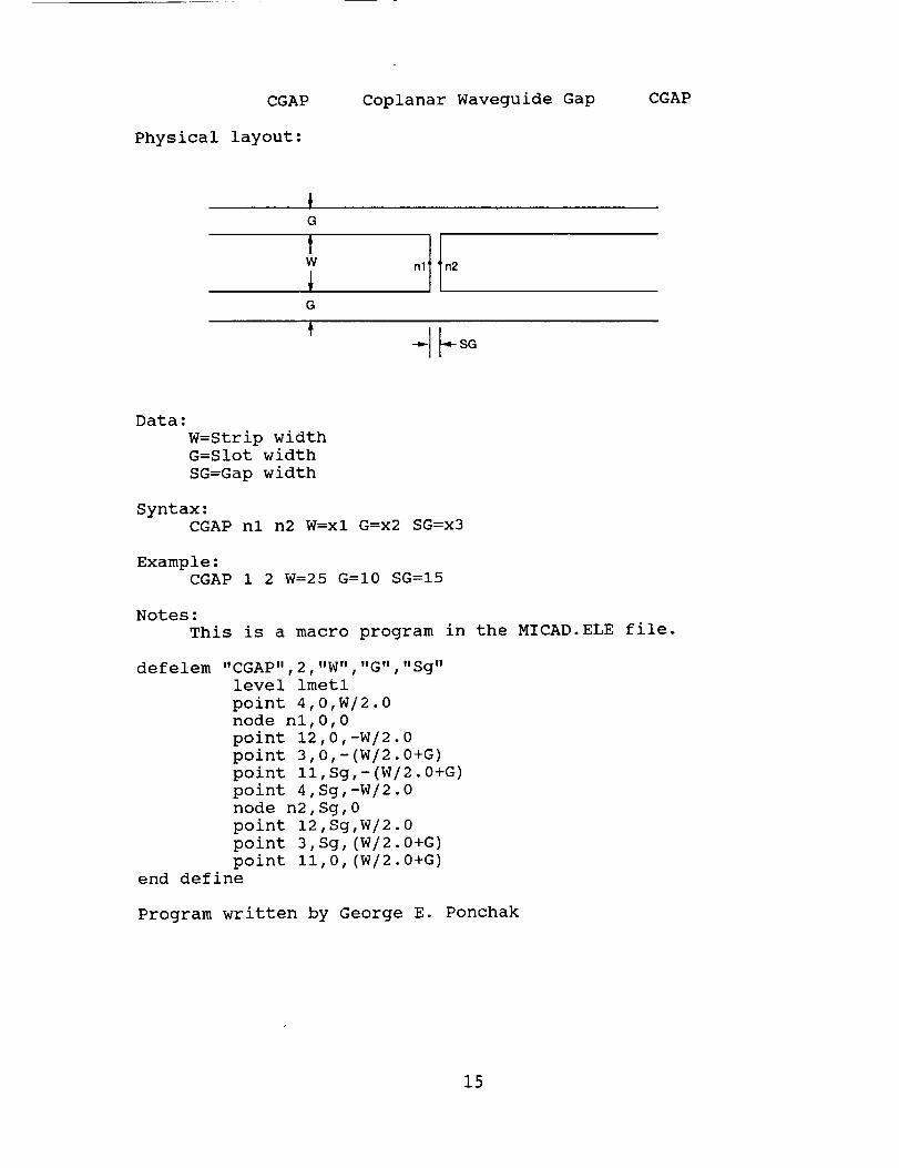
CGAP
Physical layout:
Coplanar Waveguide Gap CGAP
IG
tW
G
t
Data:
W=Strip width
G=Slot width
SG=Gap width
Syntax:
CGAP nl n2 W=xl G=x2 SG=x3
Example:
CGAP 1 2 W=25 G=I0 SG=I5
Notes:
This is a macro program in the MICAD.ELE file.
defelem "CGAP",2,"W","G","Sg"
level imetl
point 4,0,W/2.0
node nl,0,0
point 12,0,-W/2.0
point 3,0,-(W/2.0+G)
point II,Sg,-(W/2.0+G)
point 4,Sg,-W/2.0
node n2,Sg,0
point 12,Sg,W/2.0
point 3,Sg,(W/2.0+G)
point ii,0, (W/2.0+G)end define
Program written by George E. Ponchak
15


COPEN Coplanar Waveguide Open Circuit
Physical layout:
COPEN
G
tw
G
Data:
W=Strip width
G=Slot width
SO=Open end width
Syntax:COPEN nl W=xl G=x2 SO=x3
Example:COPEN 1 W=25 G=I0 SO=I0
Notes:
This is a macro program in the MICAD.ELE file.
defelem "COPEN",I,"W","G","So 'v
level imetl
point 4,0,W/2.0
node nl,O,0
point 12,0,-W/2.0
point 3,0,-(W/2.0+G)
point 8,So,-(W/2.0+G)
point 8,So,W/2.0+G
point II,O,W/2.0+Gend define
Program written by George E. Ponchak
17
PRECEDING PAGE BLANK NOT FILMED

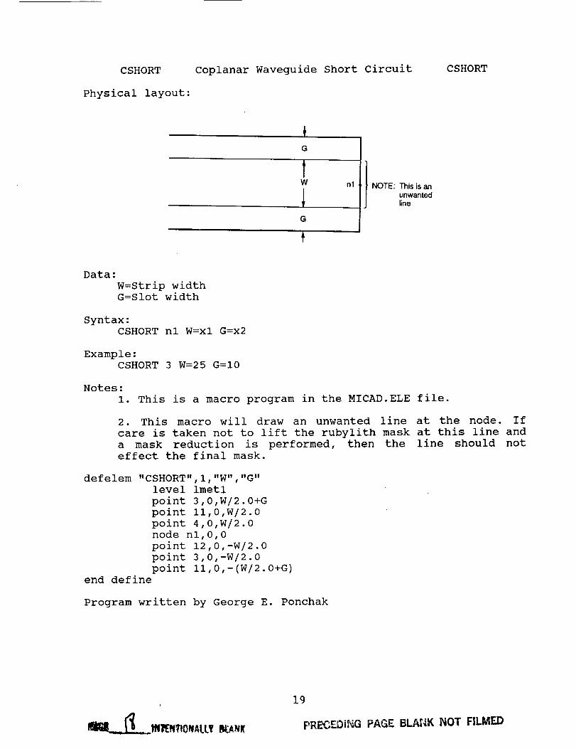
CSHORT Coplanar Waveguide Short Circuit
Physical layout:
CSHORT
+G
tw
G
nl NOTE: This is anunwantedline
Data:
W=Strip widthG=Slot width
Syntax:
CSHORT nl W=xl G=x2
Example:
CSHORT 3 W=25 G=I0
Notes:
i. This is a macro program in the MICAD.ELE file.
2. This macro will draw an unwanted line at the node. If
care is taken not to lift the rubylith mask at this line and
a mask reduction is performed, then the line should noteffect the final mask.
defelem "CSHORT",I,"W","G"
level Imetl
point 3,0,W/2.0+G
point II,0,W/2.0
point 4,0,W/2.0
node nl,0,0
point 12,0,-W/2.0
point 3,0,-W/2.0
point II,0,-(W/2.0+G)end define
Program written by George E. Ponchak
ImP__IN'I_'NTION ALLY _ANI_
19
pRE'_,EDi_'4G PAGE BLA_=4K NOT FILMED

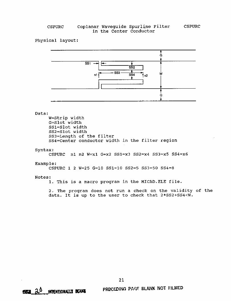
CSPURC CSPURCCoplanar Waveguide Spurline Filterin the Center Conductor
Physical layout:
nl t_ SS3"_ SS4 =i n2f
li J
W
G
Data:
W=Strip width
G=Slot width
SSI=Slot width
SS2=Slot width
SS3=Length of the filter
SS4=Center conductor width in the filter region
Syntax:CSPURC nl n2 W=xl G=x2 SSI=x3 SS2=x4 SS3=x5 SS4=x6
Example:
CSPURC 1 2 W=25 G=I0 SSI=I0 SS2=5 SS3=50 SS4=8
Notes:
i. This is a macro program in the MICAD.ELE file.
2. The program does not run a check on the validity of the
data. It is up to the user to check that 2.SS2+SS4<W.
21
pRE-_C,EDING PAGE BLANK NOT FILMED

defelem , "Ss2", "Ss3 'v, "Ss4"
end
,,CSPURCVV,2,.W,,,,,G,,,.,Ssl ,,level imetl
point 4,0,W/2.0node nl
point 8
point 8
point 8
point 8
point 8
point 8
point 8node n2
point 8
point
point
point
point
point
point
point
point
point
point
pointdefine
,0,0
,0,-W/2.0
,0,-Ss4/2.0
,Ss3,-Ss4/2.0
,Ss3,-(Ss4/2.0+Ss2)
,Ssl,-(Ss4/2.0+Ss2)
,Ssl,-W/2.0
,Ss3,-W/2.0
,Ss3,0
,Ss3,W/2.0
8,SsI,W/2.0
8,Ssl, (Ss4/2.0+Ss2)
8,Ss3, (Ss4/2.0+Ss2)
8,Ss3,Ss4/2.0
8,0,Ss4/2.0
8,0,W/2.0
12,0,W/2.0
3,0,-(W/2.0+G)
II,Ss3,-(W/2.0+G)
3,Ss3, (W/2.0+G)
ii,0, (W/2.0+G)
Program written by George E. Ponchak
22
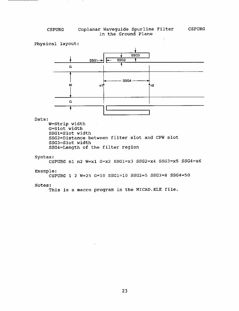
CSPURG Coplanar Waveguide Spurline Filter
in the Ground Plane
Physical layout:
CSPURG
SSGI-'-_
G
TW nl
G
Data:
W=Strip width
G=Slot width
SSGI=Slot width
p- ssa2 tSSG3 I
SSG4'n2
SSG2=Distance between filter slot and CPW slot
SSG3=Slot width
SSG4=Length of the filter region
Syntax:CSPURG nl n2 W=xl G=x2 SSGI=x3 SSG2=x4 SSG3=x5 SSG4=x6
Example:CSPURG 1 2 W=25 G=I0 SSGI=I0 SSG2=5 SSG3=8 SSG4=50
Notes:
This is a macro program in the MICAD.ELE file.
23

defelem , V,Ssg4."CSPURG",2,"W","G","SsgI","Ssg2","Ssg3"level imetlpoint 4,0,W/2.0node nl,O,Opoint 8,0,-W/2.0point 8,Ssg4,-W/2.0node n2,Ssg4,0point 8,Ssg4,W/2.0pointpointpointpointpointpointpointpoint
12,0,W/2.03,0,-(W/2.0+G)8,0,-(W/2.0+G+Ssg2+Ssg3)8,Ssg4,-(W/2.0+G+Ssg2+Ssg3)8,Ssg4,-(W/2.0+G+Ssg2)8,Ssgl,-(W/2.0+G+Ssg2)8,Ssgl,-(W/2.0+G)II,Ssg4,-(W/2.0+G)
pointpointpointpointpointpointpoint
end define
3,Ssg4, (W/2.0+G)8,SsgI,(W/2.0+G)8,Ssgl, (W/2.0+G+Ssg2)8,Ssg4, (W/2.0+G+Ssg2)8,Ssg4,(W/2.0+G+Ssg2+Ssg3)8,0, (W/2.0+G+Ssg2+Ssg3)ii,0, (W/2.0+G)
Program written by George E. Ponchak
24
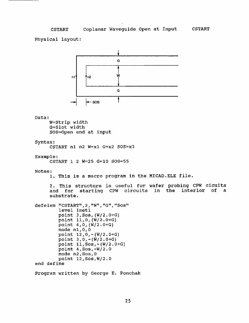
CSTART
Physical layout:
Coplanar Waveguide Open at Input
IG
G
t
CSTART
Data:
W=Strip widthG=Slot width
SOS=Open end at input
Syntax:
CSTART nl n2 W=xl G=x2 SOS=x3
Example:CSTART 1 2 W=25 G=I0 SOS=55
Notes:
i. This is a macro program in the MICAD.ELE file.
2. This structure is useful for wafer probing CPW cicuits
and for starting CPW circuits in the interior of a
substrate.
defelem "CSTART",2,"W","G","Sos"
level imetl
point 3,Sos,(W/2.0+G)
point ii,0, (W/2.0+G)
point 4,0, (W/2.0+G)
node nl,0,0
point 12,0,-(W/2.0+G)
point 3,0,-(W/2.0+G)
point ll,Sos,-(W/2.0+G)
point 4,Sos,-W/2.0
node n2,Sos,0
point 12,Sos,W/2.0end define
Program written by George E. Ponchak
25


CSTARTP CSTARTP
Physical layout:
nl
Coplanar Waveguide Open at Inputwith Pads for RF Wafer Probes
_ Pad
[-]G
W
p G,L
u---'- f_--SOS
Data:
W=Strip width
G=Slot width
SOS=Open end at input
P=Pitch of wafer probes
Pad=Side of pad
Syntax:CSTARTP nl n2 W=xl G=x2 SOS=x3 P=x4 Pad=x5
Example:CSTART 1 2 W=25 G=I0 SOS=55 P=I0 Pad=4
Notes:
i. This is a macro program in the MICAD.ELE file.
2. This structure is useful for wafer probing CPW cicuits
and for starting CPW circuits in the interior of a
substrate.
3. Cascade Microtech recommends 4 by 4 mil pads (I00 by i00
micron). The minimum recommended pad is 2 by 2 mil.
4. The pads are defined on the dielectric layer mask level.
This may be changed in the program at the commented line.
ll_i__ !NTEN TIONALLY BLANK
27
PRECEDI,r"G PAGE BLANK NOT FILMED

defelem "CSTARTP",2,"W","G","Sos","P"level imetl
point 3,Sos+Pad, (W/2.0+G)
point II,0,(W/2.0+G)
point 4,0,(W/2.0+G)
node nl,0,0
point 12,0,-(W/2.0+G)
point 3,0,-(W/2.0+G)
point ll,Sos+Pad,-(W/2.0+G)
point 4,Sos+Pad,-W/2.0
node n2,Sos+Pad,0
point 8,Sos+Pad,W/2.0
point 8,Sos,W/2.0
point 8,Sos,-W/2.0
point 12,Sos+Pad,-W/2.0
level Idiel ! defines mask layer
point 5,Sos,Pad/2.0
point 8,Sos,-Pad/2.0
point 8,Sos+Pad,-Pad/2.0
point 8,Sos+Pad,Pad/2.0
point 12,Sos,Pad/2.0
point 5,Sos,P+Pad/2.0
point 8,Sos,P-Pad/2.0
point 8,Sos+Pad,P-Pad/2.0
point 8,Sos+Pad,P+Pad/2.0
point 12,Sos,P+Pad/2.0
point 5,Sos,-P+Pad/2.0
point 8,Sos,-P-Pad/2.0
point 8,Sos+Pad,-P-Pad/2.0
point 8,Sos+Pad,-P+Pad/2.0
point 12,Sos,-P+Pad/2.0end define
, "Pad"
for pad definition
Program written by George E. Ponchak
28
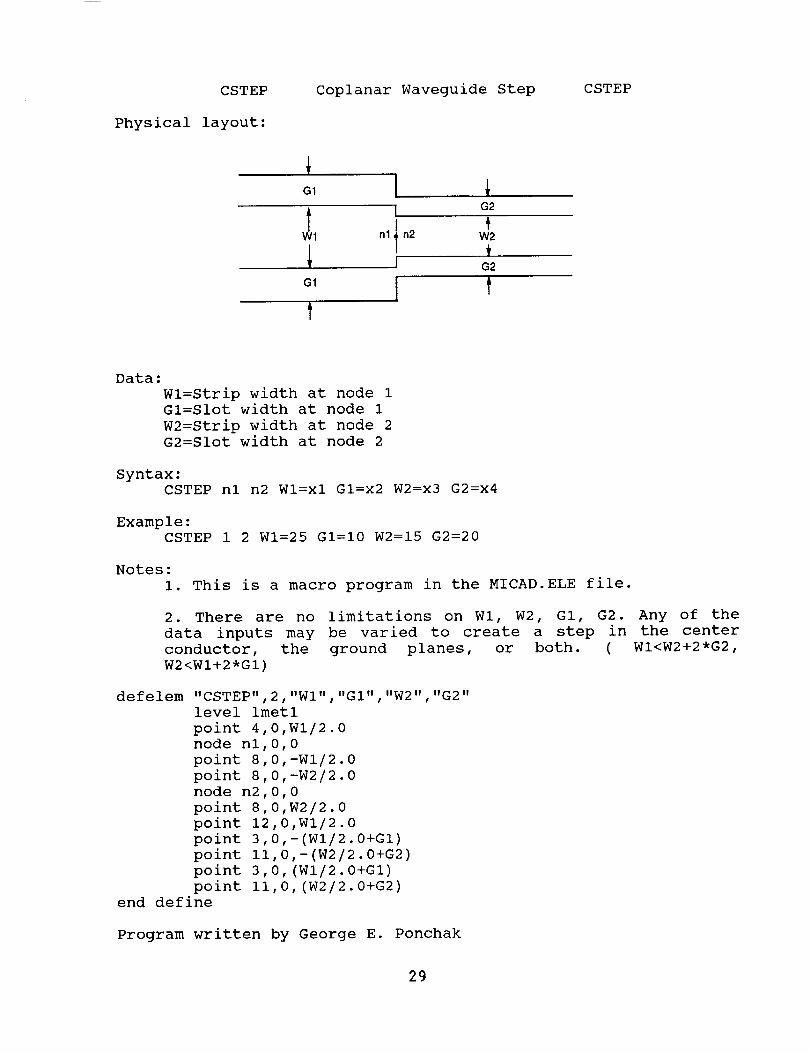
CSTEP
Physical layout:
Coplanar Waveguide Step CSTEP
GI
GI
I G2
nl n2 W2
tI G2
I t
Data:
Wl=Strip width at node 1
Gl=Slot width at node 1
W2=Strip width at node 2
G2=Slot width at node 2
Syntax:
CSTEP nl n2 Wl=xl Gl=x2 W2=x3 G2=x4
Example:
CSTEP 1 2 WI=25 GI=I0 W2=15 G2=20
Notes:
i. This is a macro program in the MICAD.ELE file.
2. There are no limitations on WI, W2, GI, G2. Any of the
data inputs may be varied to create a step in the center
conductor, the ground planes, or both. ( WI<W2+2*G2,
W2<WI+2*GI)
defelem "CSTEP",2,"WI","GI","W2","G2"
level imetl
point 4,0,WI/2.0
node nl,0,0
point 8,0,-WI/2.0
point 8,0,-W2/2.0
node n2,0,0
point 8,0,W2/2.0
point 12,0,WI/2.0
point 3,0,-(WI/2.0+GI)
point II,0,-(W2/2.0+G2)
point 3,0, (WI/2.0+GI)
point ii,0, (W2/2.0+G2)
end define
Program written by George E. Ponchak
29


CSTUBC CSTUBC
Physical layout:
Coplanar Waveguide Slot Stubin the Center Conductor
-'4 I-.-zo,G
n,.L--],n2 Wzc2 I--7
a
Data:
W=Strip width
G=Slot width
ZCl=Stub slot width
ZC2=Stub slot length
Syntax:CSTUBC nl n2 W=xl G=x2 ZCI=x3 ZC2=x4
Example:CSTUBG 1 2 W=25 G=I0 ZCI=5 ZC2=I0
Notes:
i. This is a macro program in the MICAD.ELE file.
2. The program does not run a check on the validity of the
data. It is up to the user to check that 2*ZC2<W.
31
PR;.'C.,£DIh'G PAGE BLANK NOT FILMED

defelem
end
"CSTUBC",2,"W","G","ZcI"
level imetl
point 4,0,W/2.0node nl
point 8
point 8
point 8
point 8node n2
point 8
point 8
point
point
point
point
point
pointdefine
,0,0
,0,-W/2.0
,0, (-W/2.0+Zc2)
,Zcl, (-W/2.0+Zc2)
,Zcl,-W/2.0
,Zcl,O
,Zcl,W/2.0
,Zcl, (W/2.0-Zc2)
8,0, (W/2.0-Zc2)
12,0,W/2.0
3,0,-(W/2.0+G)
II,ZcI,-(W/2.0+G)
3,Zcl, (W/2.0+G)
ii,0, (W/2.0+G)
, " ZC2 "
Program written by George E. Ponchak
32

CSTUBG CSTUBG
Physical layout:
Coplanar Waveguide Slot Stubin the Ground Plane
G
olt to2 ½, G
I I _'
ZG2
Data:
W=Strip width
G=Slot width
ZGl=Stub slot width
ZG2=Stub slot length
Syntax:
CSTUBG nl n2 W=xl G=x2 ZGI=x3 ZG2=x4
Example:
CSTUBG 1 2 W=25 G=I0 ZGI=5 ZG2=40
Notes:
This is a macro program in the MICAD.ELE file.
defelem "CSTUBG",2,"W","G","ZgI","Zg2"
level imetl
point 4,0,W/2.0
node nl,0,0
point 8,0,-W/2.0
point 8,Zgl,-W/2.0
node n2,Zgl,0
point 8,Zgl,W/2.0
point 12,0,W/2.0
point 3,0,-(W/2.0+G)
point 8,0,-(W/2.0+G+Zg2)
point 8,Zgl,-(W/2.0+G+Zg2)
point II,Zgl,-(W/2.0+G)
point 3,Zgl, (W/2.0+G)
point 8,Zgl, (W/2.0+G+Zg2)
point 8,0, (W/2.0+G+Zg2)
point ii,0, (W/2.0+G)
end define
Program written by George E. Ponchak
33


CSTUBO Coplanar Waveguide Open Ended Stub
Physical layout:
CSTUBO
OS3
.-- OS2G
n2 W
Data:
W=Strip widthG=Slot width
OSl=Stub width
OS2=Slot width of stub
OS3=Open end width
OS4=Stub length
Syntax:
CSTUBO nl n2 W=xl G=x20Sl=x3 OS2=x4 OS3=x5 0S4=x6
Example:
CSTUBO 1 2 W=25 G=10 0SI=20 OS2=I0 0S3=I0 OS4=30
Notes:
This is a macro program in the MICAD.ELE file.
EN t0mN.LY
35
PRE'CEDi[_!G PAGE BLANK NOT FILMED

defelem "CSTUBO",2,"W","G","OSI","OS2"dim OS5
dim OS6
0S5=OSI+2.0,OS2
OS6=OSI+OS2
level imetl
point 4,0,W/2.0
node nl,0,0
point 8,0,-W/2.0
point 8,0S2,-W/2.0
point 8,OS2,-(W/2.0+OS4)
point 8,0S6,-(W/2.0+OS4)
point 8,OS6,-W/2.0
point 8,0S5,-W/2.0
node n2,OS5,0
point 8,OS5,W/2.0
point 8,OS6,W/2.0
point 8,0S6, (W/2.0+OS4)
point 8,OS2, (W/2.0+0S4)
point 8,0S2,W/2.0
point 12,0,W/2.0
point 3,0,-(W/2.0+G)
point 8,0,-(W/2.0+OS3+0S4)
point 8,0S5,-(W/2.0+OS3+0S4)
point II,OS5,-(W/2.0+G)
point 3,0S5, (W/2.0+G)
point 8,OS5, (W/2.0+OS3+0S4)
point 8,0, (W/2.0+OS3+0S4)
point ii,0, (W/2.0+G)end define
Program written by George E. Ponchak
,"0S3" , "OS4"
36

CSTUBS CSTUBS
Physical layout:
Coplanar Waveguide Short CircuitTerminated Stub
asG
f t: 'nl "_. 2 W
N
l \ ,,
_-- NOTE: This is
an unwantedline
Data:
W=Strip width
G=Slot width
WS=Strip width Of stub
GS=Slot width of stub
S=Stub length
Syntax:
CSTUBS nl n2 W=xl G=x2 GS=x3 WS=x4 S=x5
Example:
CSTUBS 1 2 W=25 G=I0 GS=8 WS=I6 S=30
Notes:
i. This is a macro program in the MICAD.ELE file.
2. This macro will draw two unwanted lines at the nodes. If
care is taken not to lift the rubylith mask at these lines
and a mask reduction is performed, then these lines should
not effect the final mask.
37
defelem
end
"CSTUBS",2,"W","G","GS","WS","S"dim X
level imetl
X=2.0*GS+WS
point 4,0,W/2.0
node nl,0,0
point 12,0,-W/2.0
point 4,X,-W/2.0
node n2,X,0
point
point
point
point
point
point
point
point
point
point
point
point
point
point
point
point
point
point
point
point
pointdefine
12,X,W/2.0
3,0,-(W/2.0+G)
8,o,-(w/2.o+s)8,GS, - (W/2.0+S)
8,GS,-W/2.0
II,0,-W/2.0
3,X,-W/2.0
8,GS+WS,-W/2.0
8,GS+WS,-(W/2.0+S)
8,X,-(W/2.0+S)
II,X,-(W/2.0+G)
3,X,W/2.0+G
8,X,W/2.0+S
8,GS+WS,W/2.0+S
8,GS+WS,W/2.0
II,X,W/2.0
3,0,W/2.0
8,GS,W/2.0
8,GS,W/2.0+S
8,0,W/2.0+S
II,0,W/2.0+G
Program written by George E. Ponchak
38
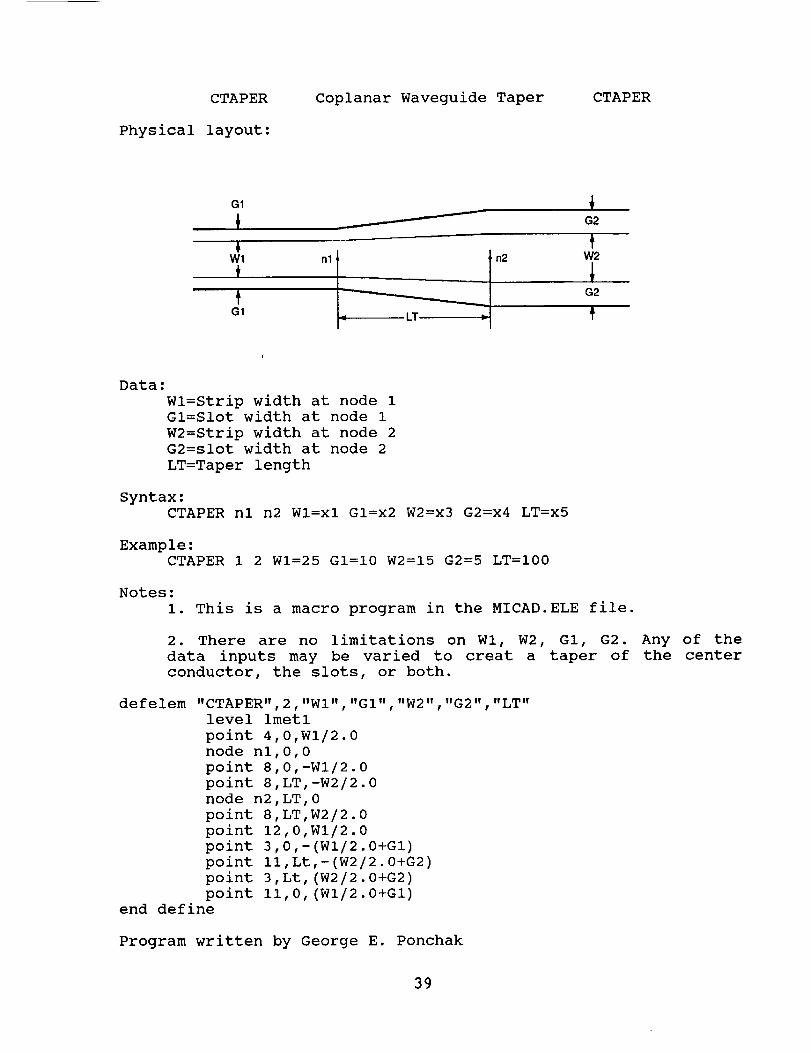
CTAPER
Physical layout:
Coplanar Waveguide Taper CTAPER
GI
G2
Wl
GI
n2 W2
G2
Data:
Wl=Strip width at node 1
Gl=Slot width at node 1
W2=Strip width at node 2
G2=slot width at node 2
LT=Taper length
Syntax:CTAPER nl n2 WI=xl Gl=x2 W2=x3 G2=x4 LT=x5
Example:CTAPER 1 2 WI=25 GI=I0 W2=15 G2=5 LT=I00
Notes:
i. This is a macro program in the MICAD.ELE file.
2. There are no limitations on WI, W2, GI, G2. Any of the
data inputs may be varied to creat a taper of the center
conductor, the slots, or both.
defelem "CTAPER",2,"WI","GI","W2","G2","LT"level imetl
point 4,0,Wi/2.0
node nl,0,0
point 8,0,-WI/2.0
point 8,LT,-W2/2.0
node n2,LT,0
point 8,LT,W2/2.0
point 12,0,WI/2.0
point 3,0,-(WI/2.0+GI)
point II,Lt,-(W2/2.0+G2)
point 3,Lt, (W2/2.0+G2)
point ii,0, (WI/2.0+GI)end define
Program written by George E. Ponchak
39


CTEEI Coplanar Waveguide T Junction CTEEI
Physical layout:
G21W2 n2
G2 nlg
._Gl_,..._-Wlo
Tn3 W3
&G3T
..,z--G1-i
Data:
Wl=Strip width at node 1Gl=Slot width at node 1
W2=Strip width at node 2G2=Slot width at node 2
W3=Strip width at node 3G3=Slot width at node 3
Syntax:CTEE nl n2 n3 Wl=xl Gl=x2 W2=x3 G2=x4 W3=x5 G3=x6
Example:CTEE 1 2 3 WI=25 GI=I0 W2=20 G2=I0 W3=30 G3=5
Notes:
i. This is a macro program in the MICAD.ELE file.
2. This Tee junction aligns the slot opposite node i. Nodes
2 and 3 may not be aligned.
41
Ft,.:_,..D,,.u PAGE BLANK NOT FILMED

defelem "CTEEIV',3,"WI","GI","W2","G2","W3","G3 ''dim d
if 2*G3+W3-2*G2-W2 > 0 then
d=O
else
d=2*G3+W3-2*G2-W2
end if
level imetl
point 4,-Wl/2,d
node nl,0,d
point 8,Wl/2,d
point 8,WI/2,G3
point 8,WI/2+GI,G3
node n3,WI/2+GI,G3+W3/2
point 8,WI/2+GI,G3+W3
point 8,0,G3+W3
point 8,0,2*G3+W3"G2
point 8,-(WI/2+GI),2*G3+W3-G2
node n2,-(WI/2+GI),2*G3+W3-G2-W2/2
point
point
point
point
point
point
point
point
point
end define
8,-(WI/2+GI),2*G3+W3-G2-W2
8,-WI/2,2*G3+W3-G2-W2
12,-Wl/2,d
3,WI/2+GI,d
II,WI/2+GI,0
3,-(WI/2+GI),2*G3+W3-2*G2-W2
ll,-(Wl/2+Sl),d
3,WI/2+GI,2*G3+W3
II,-(WI/2+GI),2*G3+W3
Program written by Nikola Visic
42

CTEE2 Coplanar Waveguide T Junction CTEE2
Physical layout:
G2
IW2 n2
G2
_G 1_
nl
_-W1 _
&!
n3 W3
__ f
q-G1-
Data:
Wl=Strip width at node 1Gl=Slot width at node 1
W2=Strip width at node 2
G2=Slot width at node 2
W3=Strip width at node 3
G3=Slot width at node 3
Syntax:CTEE nl n2 n3 Wl=xl Gl=x2 W2=x3 G2=x4 W3=x5 G3=x6
Example:CTEE 1 2 3 WI=25 GI=I0 W2=20 G2=I0 W3=30 G3=5
Notes:
i. This is a macro program in the MICAD.ELE file.
2. This Tee junction aligns nodes 2 and 3.
43
defelem
end
"CTEE2",3,"WI","GI","W2","G2","W3","G3"
dim d2,d3,d
d=G2+W2/2.0-(G3+W3/2.0)if d<=0 then
d2=-d
d3=0.O
else
d2=O.O
d3=d
end if
level imetl
point 4,0,Wi/2.0
node nl
point 8
point 8
point 8node n3
point 8
point 8
point 8
point 8node n2
point
point
point
point
point
point
point
point
point
point
pointdefine
,0,0
,0,-WI/2.0
,d3+G3,-WI/2.0
,d3+G3,-(WI/2.0+GI)
,d3+G3+W3/2.0,-(WI/2.0+GI)
,d3+G3+W3,-(WI/2.0+GI)
,d3+G3+W3,0
,d2+G2+W2,0
,d2+G2+W2,WI/2.0+GI
,d2+G2+W2/2.0,WI/2.0+GI
8,d2+G2,WI/2.0+GI
8,d2+G2,WI/2.0
12,0,WI/2.0
3,0,WI/2.0+GI
II,d2,WI/2.0+GI
3,0,-(WI/2.0+GI)
II,d3,-(Wi/2.0+GI)
3,d3+2.0*G3+W3,-(WI/2.0+GI)
8,d3+2.0*G3+W3,0
8,d2+2.0*G2+W2,0
II,d2+2.0*G2+W2,WI/2.0+GI
Program written by George E. Ponchak
44

Report Documentation PageNational Aeronautics andSpace Administralion
1. Report No.
NASA TM-103272
2. Government Accession No.
4. Title and Subtitle
Coplanar Waveguide EEsoF MICAD Macros Make Circuit Layout Easy
7. Author(s)
George E. Ponchak and Nikola Visic
9. Performing Organization Name and Address
National Aeronautics and Space AdministrationLewis Research Center
Cleveland, Ohio 44135-3191
12. Sponsoring Agency Name and Address
National Aeronautics and Space Administration
Washington, D.C. 20546-0001
3. Reciplent's Catalog No.
5. Report Date
September 1990
6. Performing Organization Code
8. Performing Organization Report No.
E-5714
10. Work Unit No.
506-44-2B
11. Contract or Grant No.
13. Type of Report and Period Covered
Technical Memorandum
14. Sponsoring Agency Code
15. Supplementary Notes
George E. Ponchak, Lewis Research Center. Nikola Visic, Cleveland State University, Cleveland, Ohio 44115,and Co-op student at Lewis Research Center.
16. Abstract
A collection of macro files is presented which permit the layout of coplanar waveguide integrated circuits usingEEsoF MICAD CAD software. The files must be added to the users MICAD.ELE file.
17. Key Words (Suggested by Author(s))
Microwave
Transmission lines
Integrated circuits
18. Distribution Statement
Unclassified - Unlimited
Subject Category 32
19. Security Classif. (of this report) 20. Security Classif. (of this page) 21. No. of pages 22. Price*
Unclassified Unclassified 48 A03
NASAFO_M162eoct 86 *For sale by the National Technical Information Service, Springfield, Virginia 22161