7. Circuit Operating Descriptions - Diagramas dediagramas.diagramasde.com/otros/Circuit...
54
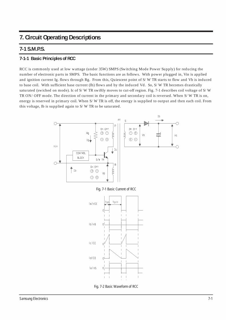
Samsung Electronics 7-1 7. Circuit Operating Descriptions 7-1 S.M.P.S. Fig. 7-1 Basic Current of RCC Fig. 7-2 Basic Waveform of RCC 7-1-1 Basic Principles of RCC RCC is commonly used at low wattage (under 35W) SMPS (Switching Mode Power Supply) for reducing the number of electronic parts in SMPS. The basic functions are as follows. With power plugged in, Vin is applied and ignition current Ig. flows through Rg. From this, Quiescent point of S/W TR starts to flow and Vb is induced to base coil. With sufficient base current (Ib) flows and by the induced Vd. So, S/W TR becomes drastically saturated (swiched on mode). Ic of S/W TR swiftly moves to cut-off region. Fig. 7-1 describes coil voltage of S/W TR ON/OFF mode. The direction of current in the primary and secondary coil is reversed. When S/W TR is on, energy is reserved in primary coil. When S/W TR is off, the energy is supplied to output and then each coil. From this voltage, Ib is supplied again to S/W TR to be saturated.
Transcript of 7. Circuit Operating Descriptions - Diagramas dediagramas.diagramasde.com/otros/Circuit...
Samsung Electronics 7-1
7. Circuit Operating Descriptions
7-1 S.M.P.S.
Fig. 7-1 Basic Current of RCC
Fig. 7-2 Basic Waveform of RCC
7-1-1 Basic Principles of RCC
RCC is commonly used at low wattage (under 35W) SMPS (Switching Mode Power Supply) for reducing thenumber of electronic parts in SMPS. The basic functions are as follows. With power plugged in, Vin is appliedand ignition current Ig. flows through Rg. From this, Quiescent point of S/W TR starts to flow and Vb is inducedto base coil. With sufficient base current (Ib) flows and by the induced Vd. So, S/W TR becomes drastically saturated (swiched on mode). Ic of S/W TR swiftly moves to cut-off region. Fig. 7-1 describes coil voltage of S/WTR ON/OFF mode. The direction of current in the primary and secondary coil is reversed. When S/W TR is on,energy is reserved in primary coil. When S/W TR is off, the energy is supplied to output and then each coil. Fromthis voltage, Ib is supplied again to S/W TR to be saturated.
Circuit Operating Descriptions
7-2 Samsung Electronics
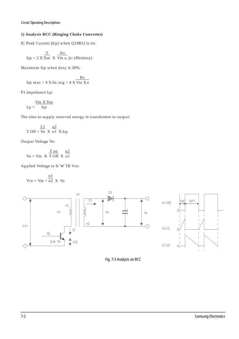
Fig. 7-3 Analysis on RCC
1) Analysis RCC (Ringing Choke Converter)
IC Peak Current (Icp) when Q1SR12 is on:
T PoIcp = 2 X Ton X Vin e, (e: efficiency)
Maximum Icp when duty is 50%:
PoIcp max = 4 X lin avg = 4 X Vin X e
P1 impedance Lp:
Vin X TonLp = Icp
The time to supply reserved energy in transformer to output:
L1 n2T Off = Vo X n1 X Icp
Output Voltage Vo:
T on n2Vo = Vin X T Off X n1
Applied Voltage to S/W TR Vce:
n1Vce = Vin + n2 X Vo
Circuit Operating Descriptions
Samsung Electronics 7-3
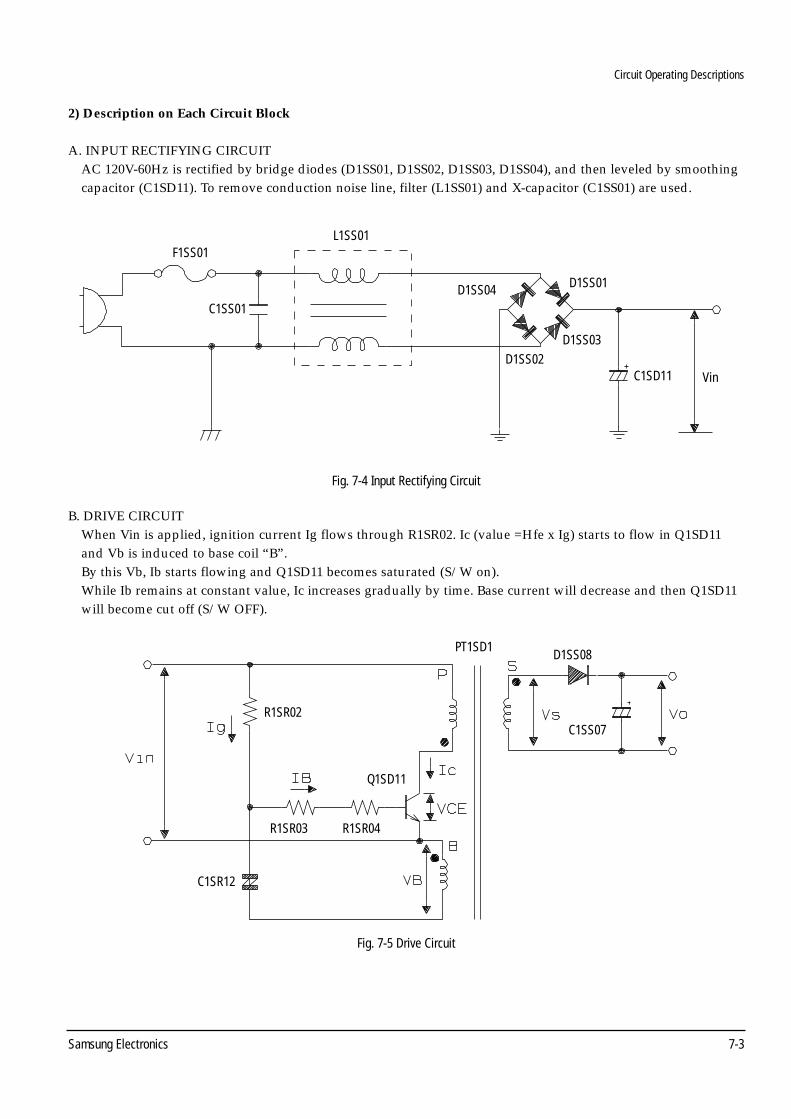
Fig. 7-5 Drive Circuit
Fig. 7-4 Input Rectifying Circuit
B. DRIVE CIRCUITWhen Vin is applied, ignition current Ig flows through R1SR02. Ic (value =Hfe x Ig) starts to flow in Q1SD11 and Vb is induced to base coil “B”. By this Vb, Ib starts flowing and Q1SD11 becomes saturated (S/W on).While Ib remains at constant value, Ic increases gradually by time. Base current will decrease and then Q1SD11 will become cut off (S/W OFF).
F1SS01L1SS01
C1SS01
C1SD11 VinD1SS02
D1SS03
D1SS04 D1SS01
R1SR02
C1SR12
R1SR03 R1SR04
Q1SD11
D1SS08
C1SS07
PT1SD1
2) Description on Each Circuit Block
A. INPUT RECTIFYING CIRCUITAC 120V-60Hz is rectified by bridge diodes (D1SS01, D1SS02, D1SS03, D1SS04), and then leveled by smoothing capacitor (C1SD11). To remove conduction noise line, filter (L1SS01) and X-capacitor (C1SS01) are used.
Circuit Operating Descriptions
7-4 Samsung Electronics
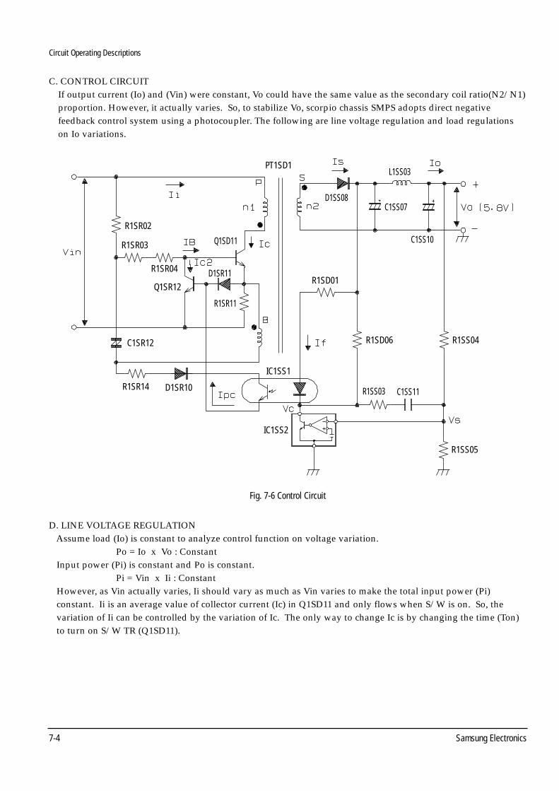
Fig. 7-6 Control Circuit
R1SR02
R1SR03
R1SR04
Q1SR12
C1SR12
R1SR14 D1SR10
IC1SS2
IC1SS1
R1SR11
D1SR11
Q1SD11
R1SD01
R1SD06
R1SS03 C1SS11
R1SS05
R1SS04
PT1SD1
D1SS08
L1SS03
C1SS07
C1SS10
D. LINE VOLTAGE REGULATIONAssume load (Io) is constant to analyze control function on voltage variation.
Po = Io x Vo : ConstantInput power (Pi) is constant and Po is constant.
Pi = Vin x Ii : ConstantHowever, as Vin actually varies, Ii should vary as much as Vin varies to make the total input power (Pi) constant. Ii is an average value of collector current (Ic) in Q1SD11 and only flows when S/W is on. So, thevariation of Ii can be controlled by the variation of Ic. The only way to change Ic is by changing the time (Ton)to turn on S/W TR (Q1SD11).
C. CONTROL CIRCUITIf output current (Io) and (Vin) were constant, Vo could have the same value as the secondary coil ratio(N2/N1)proportion. However, it actually varies. So, to stabilize Vo, scorpio chassis SMPS adopts direct negative feedback control system using a photocoupler. The following are line voltage regulation and load regulationson Io variations.
Circuit Operating Descriptions
Samsung Electronics 7-5
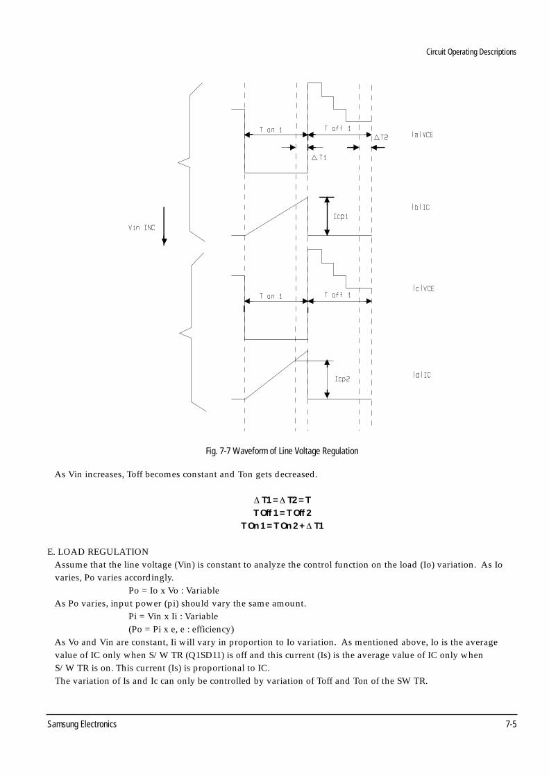
Fig. 7-7 Waveform of Line Voltage Regulation
As Vin increases, Toff becomes constant and Ton gets decreased.
∆ T1 = ∆ T2 = TT Off 1 = T Off 2
T On 1 = T On 2 + ∆ T1
E. LOAD REGULATIONAssume that the line voltage (Vin) is constant to analyze the control function on the load (Io) variation. As Io varies, Po varies accordingly.
Po = Io x Vo : VariableAs Po varies, input power (pi) should vary the same amount.
Pi = Vin x Ii : Variable(Po = Pi x e, e : efficiency)
As Vo and Vin are constant, Ii will vary in proportion to Io variation. As mentioned above, Io is the average value of IC only when S/W TR (Q1SD11) is off and this current (Is) is the average value of IC only when S/W TR is on. This current (Is) is proportional to IC.The variation of Is and Ic can only be controlled by variation of Toff and Ton of the SW TR.
Circuit Operating Descriptions
7-6 Samsung Electronics
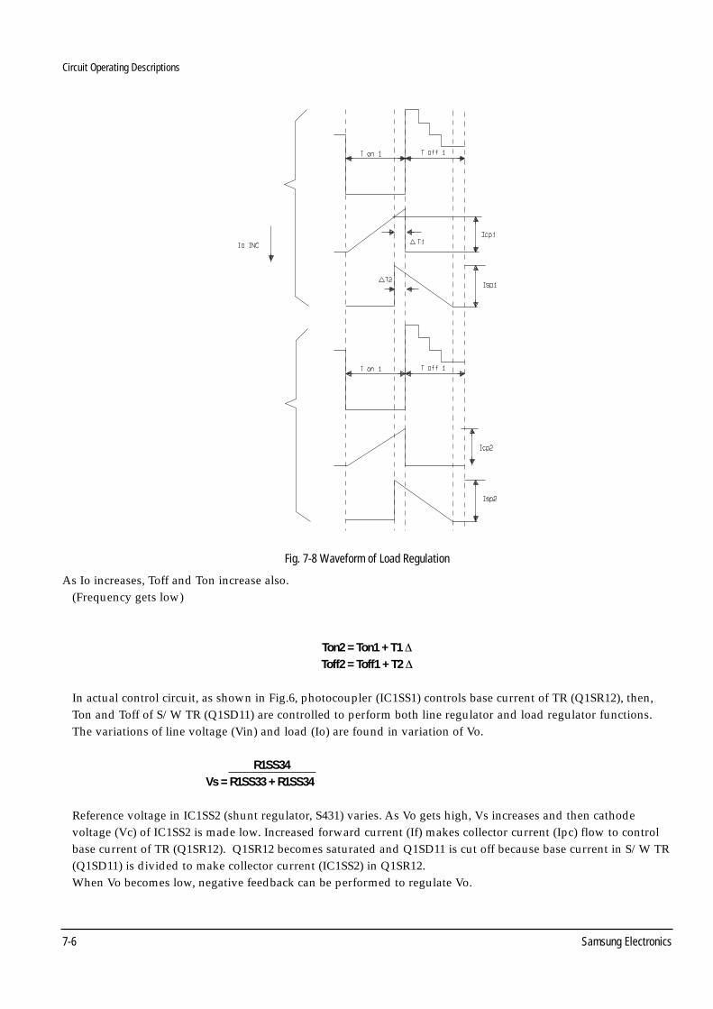
Fig. 7-8 Waveform of Load Regulation
As Io increases, Toff and Ton increase also.(Frequency gets low)
Ton2 = Ton1 + T1 ∆Toff2 = Toff1 + T2 ∆
In actual control circuit, as shown in Fig.6, photocoupler (IC1SS1) controls base current of TR (Q1SR12), then, Ton and Toff of S/W TR (Q1SD11) are controlled to perform both line regulator and load regulator functions. The variations of line voltage (Vin) and load (Io) are found in variation of Vo.
R1SS34Vs = R1SS33 + R1SS34
Reference voltage in IC1SS2 (shunt regulator, S431) varies. As Vo gets high, Vs increases and then cathode voltage (Vc) of IC1SS2 is made low. Increased forward current (If) makes collector current (Ipc) flow to control base current of TR (Q1SR12). Q1SR12 becomes saturated and Q1SD11 is cut off because base current in S/W TR (Q1SD11) is divided to make collector current (IC1SS2) in Q1SR12. When Vo becomes low, negative feedback can be performed to regulate Vo.
Circuit Operating Descriptions
Samsung Electronics 7-7
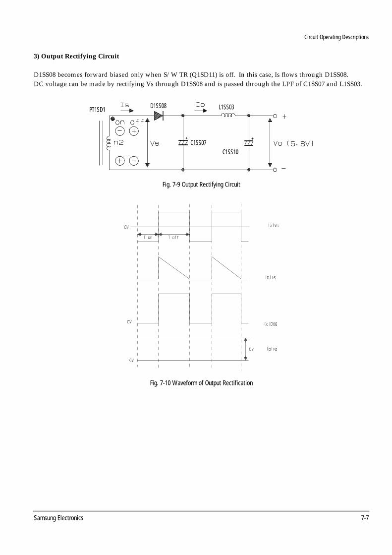
Fig. 7-9 Output Rectifying Circuit
Fig. 7-10 Waveform of Output Rectification
3) Output Rectifying Circuit
D1SS08 becomes forward biased only when S/W TR (Q1SD11) is off. In this case, Is flows through D1SS08.DC voltage can be made by rectifying Vs through D1SS08 and is passed through the LPF of C1SS07 and L1SS03.
D1SS08
C1SS07C1SS10
L1SS03PT1SD1
Circuit Operating Descriptions
7-8 Samsung Electronics
Fig. 7-12 Vce of Q1
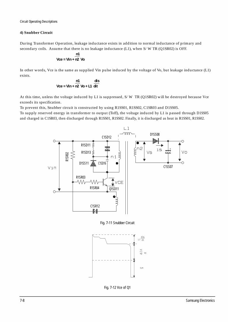
Fig. 7-11 Snubber Circuit
R1SR
02
D1SS08
C1SS07
C1SD12
C1SR12
Q1SD11
R1SR03
R1SR04
C1SD16D1SS11
R1SD13
R1SD11
4) Snubber Circuit
During Transformer Operation, leakage inductance exists in addition to normal inductance of primary and secondary coils. Assume that there is no leakage inductance (L1), when S/W TR (Q1SR02) is OFF.
n1Vce = Vin + n2 Vo
In other words, Vce is the same as supplied Vin pulse induced by the voltage of Vo, but leakage inductance (L1)exists.
n1 disVce = Vin + n2 Vo + L1 dit
At this time, unless the voltage induced by L1 is suppressed, S/W TR (Q1SR02) will be destroyed because Vceexceeds its specification. To prevent this, Snubber circuit is constructed by using R1SS01, R1SS02, C1SR03 and D1SS05. To supply reserved energy in transformer to output (Toff), the voltage induced by L1 is passed through D1SS05and charged in C1SR03, then discharged through R1SS01, R1SS02. Finally, it is discharged as heat in R1SS01, R1SS02.
Circuit Operating Descriptions
Samsung Electronics 7-9
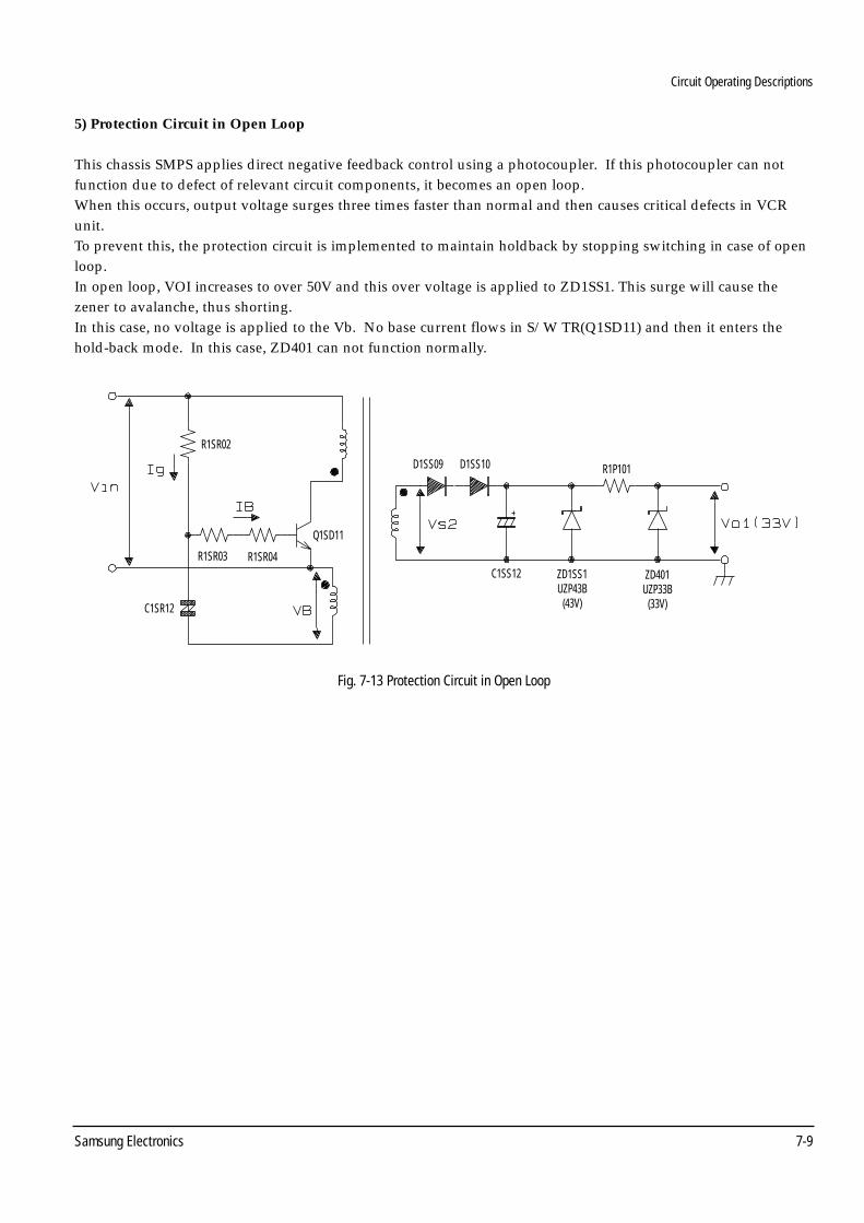
5) Protection Circuit in Open Loop
This chassis SMPS applies direct negative feedback control using a photocoupler. If this photocoupler can notfunction due to defect of relevant circuit components, it becomes an open loop. When this occurs, output voltage surges three times faster than normal and then causes critical defects in VCRunit. To prevent this, the protection circuit is implemented to maintain holdback by stopping switching in case of openloop. In open loop, VOI increases to over 50V and this over voltage is applied to ZD1SS1. This surge will cause thezener to avalanche, thus shorting. In this case, no voltage is applied to the Vb. No base current flows in S/W TR(Q1SD11) and then it enters thehold-back mode. In this case, ZD401 can not function normally.
Fig. 7-13 Protection Circuit in Open Loop
R1SR02
R1P101D1SS09 D1SS10
ZD1SS1UZP43B
(43V)
ZD401UZP33B
(33V)
C1SS12
C1SR12
R1SR03 R1SR04
Q1SD11
Circuit Operating Descriptions
7-10 Samsung Electronics
7-2 VCR System Control
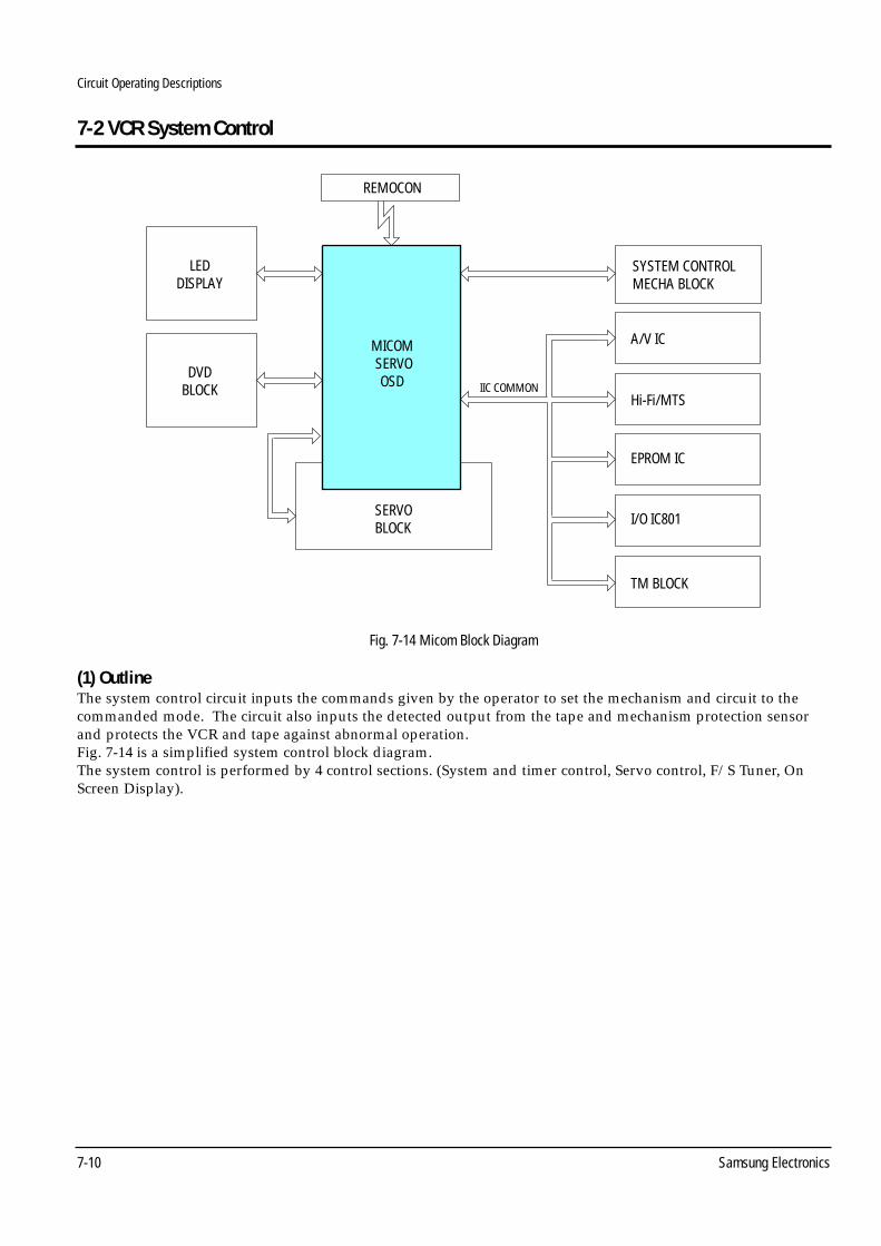
Fig. 7-14 Micom Block Diagram
(1) OutlineThe system control circuit inputs the commands given by the operator to set the mechanism and circuit to thecommanded mode. The circuit also inputs the detected output from the tape and mechanism protection sensorand protects the VCR and tape against abnormal operation. Fig. 7-14 is a simplified system control block diagram. The system control is performed by 4 control sections. (System and timer control, Servo control, F/S Tuner, OnScreen Display).
LEDDISPLAY
DVDBLOCK
REMOCON
SYSTEM CONTROLMECHA BLOCK
Hi-Fi/MTS
A/V IC
I/O IC801
EPROM IC
TM BLOCK
IIC COMMON
MICOM SERVO
OSD
SERVOBLOCK
Circuit Operating Descriptions
Samsung Electronics 7-11
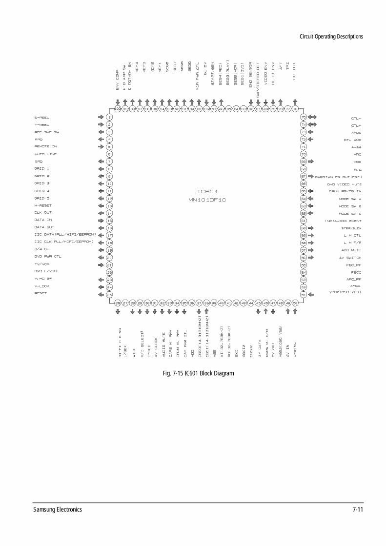
Fig. 7-15 IC601 Block Diagram
Circuit Operating Descriptions
7-12 Samsung Electronics
(2) Mechanism/Circuit ControlWhen the u-COM inputs operator’s commands via the key input or remote input, the mechanism and circuits areset to the command mode. This function controls mechanism/servo section and audio/video processing section.
1) Cassette Loading ControlControls loading and ejection of a cassette and determines the mechanism operation mode; tape loading/unloading, action/release of various breaks, tension, take up mechanism etc.
2) Tape Protection Sensor MonitoringDetects abnormal operation in tape using the supply and take up end sensor, reel sensor and SW 30Hz pulse for drum rotation.
3) Capstan Motor ControlDetermines the tape speed and direction, fast forwards and rewinds the tape etc.
4) Tape Counter ControlCounts the control pulses on the control track, picked up by the control head and shows it on the digitalmultidisplay.
5) Servo ControlDetermines the operation mode of the servo circuit. Control the speed of drum and capstan motor, and then Control the phase of drum and capstan motor.
6) Record Safety Tap DetectionDetects the safety tab on the rear of a cassette to prevent a prerecorded program from being erased.
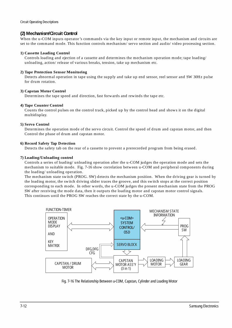
7) Loading/Unloading controlControls a series of loading/unloading operation after the u-COM judges the operation mode and sets themechanism to suitable mode. Fig. 7-16 show correlation between u-COM and peripheral components during the loading/unloading operation.The mechanism state switch (PROG. SW) detects the mechanism position. When the driving gear is turned by the loading motor, the switch driving slider traces the groove, and this switch stops at the correct position corresponding to each mode. In other words, the u-COM judges the present mechanism state from the PROG SW after receiving the mode data, then it outputs the loading motor and capstan motor control signals. This continues until the PROG SW reaches the correct state by the u-COM.
<u-COM>SYSTEM
CONTROL/OSD
FUNCTION-TIMER
CAPSTAN / DRUMMOTOR
CAPSTANMOTOR ASS’Y
(3 in 1)
DFG,DFGCFG
SERVO BLOCK
LOADINGMOTOR
LOADINGGEAR
PROGSW
MECHANISM STATEINFORMATION
OPERATIONMODEDISPLAY
AND
KEYMATRIX
Fig. 7-16 The Relationship Between u-COM, Capstan, Cylinder and Loading Motor

Circuit Operating Descriptions
Samsung Electronics 7-13
Table 1 : Prog. SW State in Each Mode
(3) Program SW InputThe mechanism state for each mode is shown in table 1 below. The mechanism state is classified into position, andcorrelation between the switch position and mechanism state is shown in table 1, also.
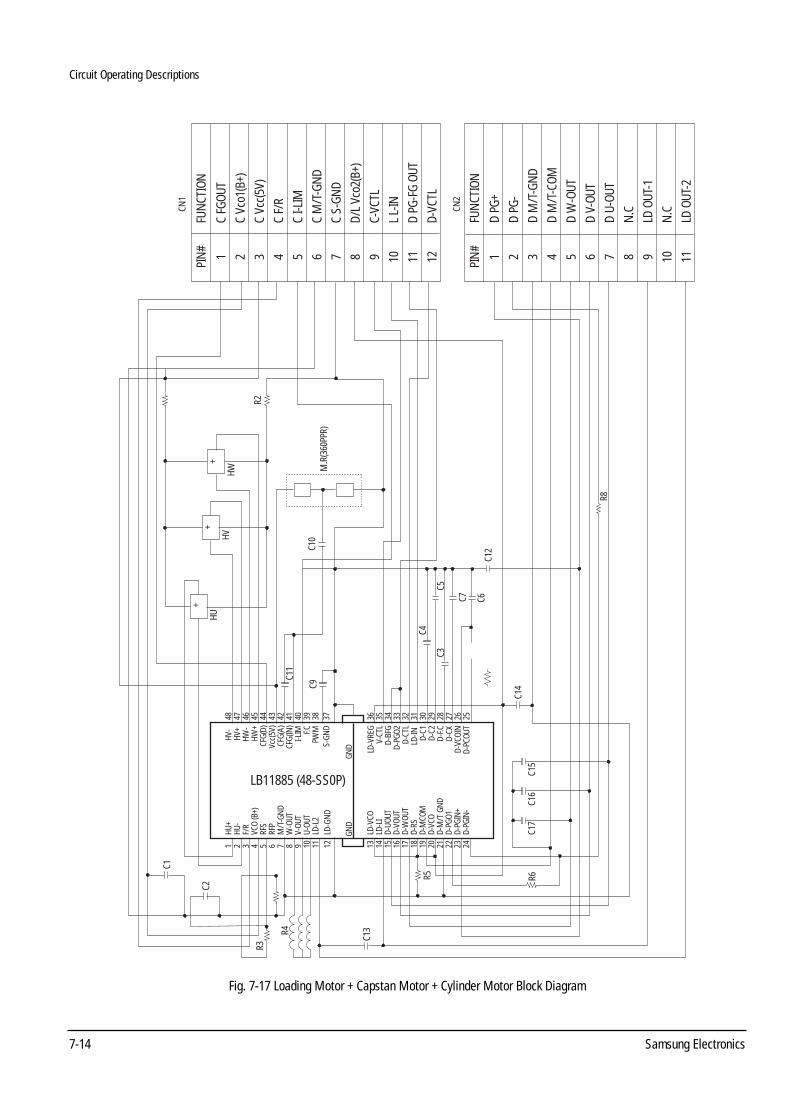
(4) Motor ControlIn case of Scorpio-2 Deck, Loading Motor Drive IC lies in Capstan Motor, not like Scorpio-1 Deck.In detail, Capstan Motor Drive IC is designed to drive Loading Motor + Capstan Motor + Cylinder Motor in oneIC. (See Fig. 7-17)
Table 2 : Motor Control Logic
POSIONCAM S/W START
ACTION MODEA B C SEN
STANBY 0 0 0 0 EjectPOWER OFF 0 0 0 1 Unload POWER OFF
LOADING START 0 0 0 1 (Tape loading start point)LOADING END 1 0 1 1 1 (Tape loading end point)
REV 1 1 0 X Reverse picture search, reverse SLOWPLAY 0 1 0 X Play, Rec, F-PS, Still, SLOW, F-ADV
STOP 1 0 0 1 1 Stop (Play position 5 Min. over)STOP 2 0 0 1 X (MAIN Break ON MODE)
FF/REW 1 1 0 0 X High speed Rew, Low speed FFFF/REW 2 0 1 1 X High speed FF, Low speed Rew
CN604-PIN10 MOTOR0 ~ 1V Reverse2 ~ 3V Stop4 ~ 5V Forward
Circuit Operating Descriptions
7-14 Samsung Electronics
PIN
#
1 2 3 4 5 6 7 8 9 10 11 12
FUN
CTIO
N
C FG
OUT
C Vc
o1(B
+)C
Vcc(
5V)
C F/
RC
I-LIM
C M
/T-G
ND
C S-
GND
D/L
Vco2
(B+)
C-VC
TLL
L-IN
D PG
-FG
OUT
D-VC
TL
PIN
#
1 2 3 4 5 6 7 8 9 10 11
FUN
CTIO
N
D PG
+D
PG-
D M
/T-G
ND
D M
/T-C
OMD
W-O
UTD
V-OU
TD
U-OU
TN
.CLD
OUT
-1N
.CLD
OUT
-2
13
LD-V
CO14
LD
-LI
15
D-UO
UT16
D-
VOUT
17
D-W
OUT
18
D-RS
19
D-M
COM
20
D-VC
O21
D-
M/T
GN
D22
D-
PGO1
23
D-PG
IN+
24
D-PG
IN-
1
HU+
2
HU-
3
F/R
4
VCO
(B+)
5
RFS
6
RFP
7
M/T
-GN
D8
W
-OUT
9
V-O
UT10
U-
OUT
11
LD-L
212
LD
-GN
D
HV-
48
HV+
4
7HW
- 4
6HW
+ 4
5CF
G(D)
44
Vcc(
5V)
43
CFG(
A)
42CF
G(IN
) 4
1I-L
IM
40F.C
39
PWM
38
S-GN
D 3
7
LD-V
REG
36
V-C
TL
35D-
BFG
34
D-PG
O2
33D-
CTL
32
LD-IN
3
1D-
C1
30D-
C2
29D-
F.C
28 D
-CX
27
D-VC
OIN
26
D-PC
OUT
25
GND
GND
LB11885 (48-SS0P)
R5
C13R4
R3
C2
C1
R6C1
7C1
6C1
5C1
4
C4
C3C5
C7 C6C1
2
R8
C9C1
0M
.R(3
60PP
R)
R2
CN1
CN2
HWHV
HU
++
+
C11
Fig. 7-17 Loading Motor + Capstan Motor + Cylinder Motor Block Diagram

Circuit Operating Descriptions
Samsung Electronics 7-15
(5) Stop ModeThe VCR enters the stop mode when the stop button is pressed during playback, record, rewind and fast forwardmode. When trouble is detected, the VCR enters the stop mode to protect the tape and mechanism or when thetape reaches the end, etc.• State Input ;
Power switch on position.Stop button operation in all mode, except for timer recording and XPR.
(6) Play Mode• State input ; Play button operated in stop, fast forward, rewind, forward search, reverse search, still mode, etc.,• Indication output ;
“PLAY” lights in VFD.• Output at ;
IC601 Pin 45 (CAP F/R) : H
(7) Trick Play ModeTrick play modes are classified into forward search, reverse search, still, slow and frame advance. Audio signal is muted by pin 29 of IC601 (A.MUTE). V-lock is controlled by pin 24 of IC601.
(8) Forward Search Mode7 Times play speed search in SP and SLP, 21 times play speed search in SLP.• State input ; Press the fast forward button on the VCR front panel or the remote control in play or still mode.• Indication output ; “CUE ” display in VFD during 3 seconds.• Output at ;
IC601 Pin 25 (CAP F/R) : HIC601 Pin 50 (A.MUTE) : H
(9) Reverse Search Mode7 times play speed reverse search in SP, 21 times play speed reverse search in SLP.• State input ;
Press the rewind button on the VCR front panel or on the remote control in play or still mode.• Indication output ;
“REVIEW” display in VFD during 3 seconds.• Output ;
IC601 Pin 45 (CAP F/R) : HIC601 Pin 29 (A.MUTE) : H
(10) Slow Mode• State input ; Press “ “ button and then press “ “ button on the remote control.
The slow speed can be changed when “ “ or “ “ button is pressed.• Indication output ; “SLOW” lights in VF display.• Output at ;
IC601 Pin 45 (CAP F/R) : HIC601 Pin 29 (A.MUTE) : H
Circuit Operating Descriptions
7-16 Samsung Electronics
(11) Play/Still ModeThe same track is traced by the video heads.• State input ; Press “ “ button in play modes.• Indication output ; “STILL” display in VF display.• Output at ;
IC601 Pin 45 (CAP F/R) : HIC601 Pin 29 (A.MUTE) : H
(12) Record ModeMust use a cassette with the safety tab.Index signal is recorded on the control track of the tape at the start of recording.• State input ;
Press the record button during stop mode and record pause mode or at the preset time reached in the timer record mode. Press the REC button in stop mode.
• Indication output ; “RECORD” lights in VF display in normal record mode, “OTR” display in timer XPR modes.
• Output at ;IC601 Pin 45 (CAP F/R) : H
(13) Record Pause ModeThe pinch roller is released from the capstan shaft in a moment. The brake is applied to the take up reel to prevent tape slack during the record pause mode.• State input ; Press “ “ button in the record mode.
Note : Inoperative during recording and XPR mode.• Indication output ; “PAUSE”display in VF display.
(14) Fast Forward ModeTape fast forward operation using capstan motor.• State input ; Press the rewind button in the stop or fast forward modes.• Indication output ; “FF” lights in VF display.• Output at ;
IC601 Pin 45 (CAP F/R) : H
(15) Rewind ModeTape rewind operation using the capstan motor.• State input ; Press the rewind button in the stop or fast forward modes.• Indication output ; “REWIND” lights in VF display.• Output at ;
IC601 Pin 45 (CAP F/R) : L
(16) Rewind Shut-Off ModeTape rewind operation then power off mode.• State input ; Press the power button in the rewind mode.
Circuit Operating Descriptions
Samsung Electronics 7-17
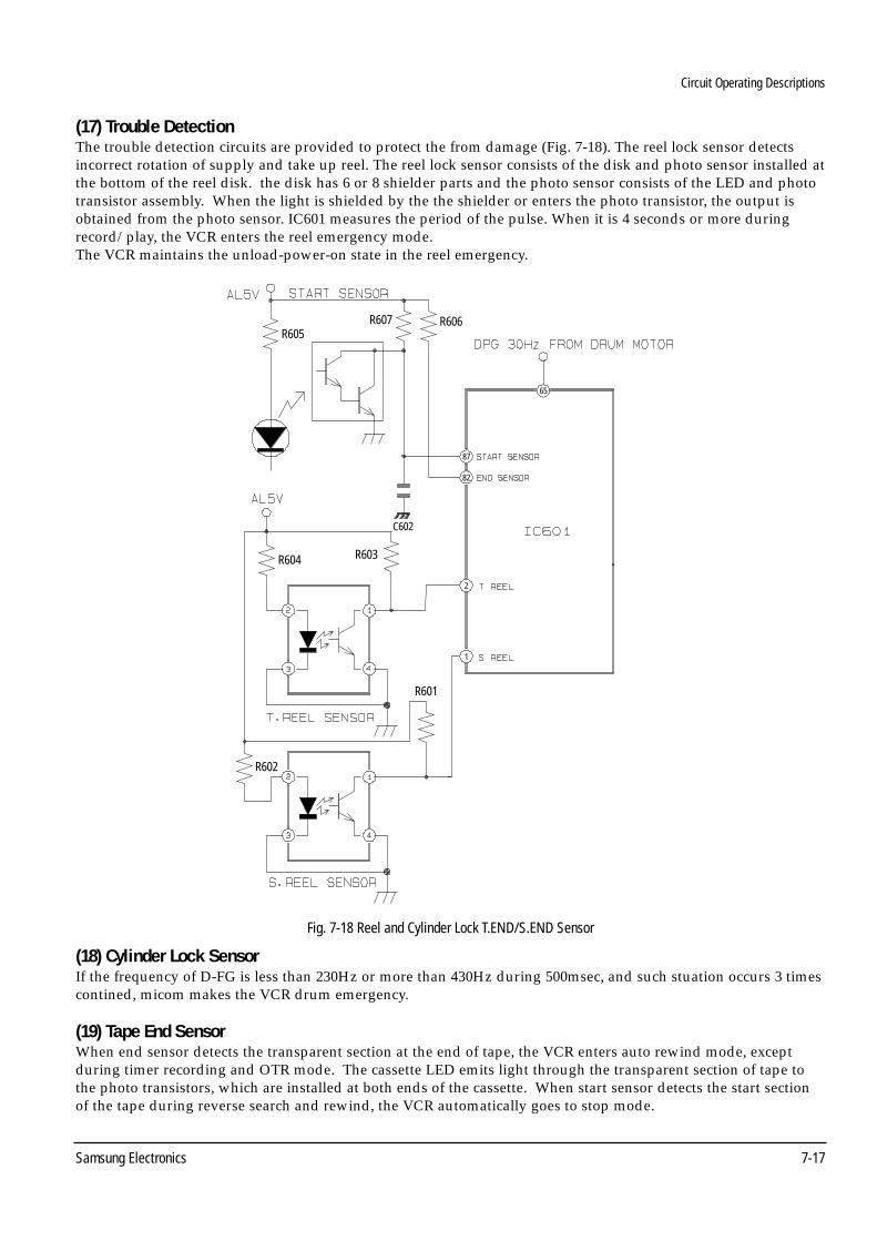
(17) Trouble DetectionThe trouble detection circuits are provided to protect the from damage (Fig. 7-18). The reel lock sensor detectsincorrect rotation of supply and take up reel. The reel lock sensor consists of the disk and photo sensor installed atthe bottom of the reel disk. the disk has 6 or 8 shielder parts and the photo sensor consists of the LED and phototransistor assembly. When the light is shielded by the the shielder or enters the photo transistor, the output isobtained from the photo sensor. IC601 measures the period of the pulse. When it is 4 seconds or more duringrecord/play, the VCR enters the reel emergency mode.The VCR maintains the unload-power-on state in the reel emergency.
Fig. 7-18 Reel and Cylinder Lock T.END/S.END Sensor
R607 R606
65
87
82
2
1
R604 R603
R602
R601
R605
C602
(18) Cylinder Lock SensorIf the frequency of D-FG is less than 230Hz or more than 430Hz during 500msec, and such stuation occurs 3 timescontined, micom makes the VCR drum emergency.
(19) Tape End SensorWhen end sensor detects the transparent section at the end of tape, the VCR enters auto rewind mode, exceptduring timer recording and OTR mode. The cassette LED emits light through the transparent section of tape tothe photo transistors, which are installed at both ends of the cassette. When start sensor detects the start sectionof the tape during reverse search and rewind, the VCR automatically goes to stop mode.

Circuit Operating Descriptions
7-18 Samsung Electronics
(20) Tape Counter ControlFig. 7-19 is a simplified diagram of the tape counter control circuit. The tape counter in the u-COM counts the control pulses derived from control head. The control signal on the control track of the tape is picked up by thecontrol head and supplied to pins 74, 75 of IC601. The control pulse is amplified by the u-COM IC. The u-COMdetermines the tape direction so the counter counts up when the “CAP F/R”signal is Hi and the counter countsdown when the “CAP F/R” signal is Low. By counting the control pulse, the counter data is supplied to the VFdisplay. Counter displays the time and it is increased or decreased by one minute after counting 1800 control puls-es. Counter mode is switched to clock mode when the display button is pushed or when the VCR goes to poweroff mode. When the Clear button is pressed, the counter is reset to “00 : 00”. The tape counter has a memory stop function.
Fig. 7-19 Counter Display
Pin 83 ~ 86/90 ~ 93 : SEGPin 8 ~ 12 : GRID
74
75
TR DiscreteCircuit Block
LED DISPLAY
Circuit Operating Descriptions
Samsung Electronics 7-19
(21) Timer/OTR ControlThe timer can preset 7 programs in one month including daily and weekly programs. Express recording lets the operator record up to 9 hours 30 minutes without programming the timer.
(22) Clock DisplayThe clock generator inside of the u-COM counts the oscillation signal of XT601 for the timer clock data.
(23) Power Failure Detectionu-COM goes to the power failure mode when the 61 port is lower than 4/5 of AD Vcc level.
(24) 4H’D ControlDuring trick play (still,slow,F-advance), it is necessary to control pre-amp,video circuit. the micom control pin 29(C-ROTARY), pin 30 (HD-AMP) of the IC601 during PB period in Slow mode. These port is applied to video IC to operate the trick play.
Circuit Operating Descriptions
7-20 Samsung Electronics
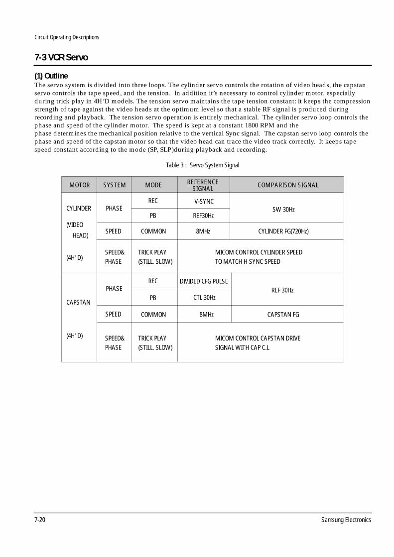
7-3 VCR Servo
(1) OutlineThe servo system is divided into three loops. The cylinder servo controls the rotation of video heads, the capstanservo controls the tape speed, and the tension. In addition it’s necessary to control cylinder motor, especially during trick play in 4H’D models. The tension servo maintains the tape tension constant: it keeps the compressionstrength of tape against the video heads at the optimum level so that a stable RF signal is produced during recording and playback. The tension servo operation is entirely mechanical. The cylinder servo loop controls thephase and speed of the cylinder motor. The speed is kept at a constant 1800 RPM and thephase determines the mechanical position relative to the vertical Sync signal. The capstan servo loop controls thephase and speed of the capstan motor so that the video head can trace the video track correctly. It keeps tapespeed constant according to the mode (SP, SLP)during playback and recording.
Table 3 : Servo System Signal
DIVIDED CFG PULSE
8MHz CAPSTAN FG
MOTOR
CYLINDER
CAPSTAN
(VIDEO
(4H' D)
(4H' D)
HEAD)SPEED
SPEED
SPEED&PHASE
SPEED&PHASE
TRICK PLAY(STILL. SLOW)
TRICK PLAY(STILL. SLOW)
MICOM CONTROL CYLINDER SPEEDTO MATCH H-SYNC SPEED
MICOM CONTROL CAPSTAN DRIVESIGNAL WITH CAP C.L
COMMON 8MHz CYLINDER FG(720Hz)
PHASE
PHASE
REC V-SYNC
REF30HzSW 30Hz
PB
COMMON
REC
PB
SYSTEM MODE COMPARISON SIGNALREFERENCESIGNAL
CTL 30HzREF 30Hz
Circuit Operating Descriptions
Samsung Electronics 7-21
Spee
d erro
rde
tectio
nHS
Wge
nerat
ion
Phas
e erro
rde
tectio
nDi
gital
filter
Digit
alfilt
erPW
Mco
nvers
ion
Digit
alfilt
erBia
s valu
ead
dition
RECC
TLge
nerat
ion
Phas
ede
tectio
nDi
gital
filter
Spee
d erro
rde
tectio
n
PBCT
Lam
plifie
r
RECC
TLhe
ad
Kp Kp KvKv
(Drum
spee
d gain
)
(Drum
phas
e gain
)
(Caps
tan ph
ase g
ain)
CFG
ampli
fier
VSYNC
separa
tioncirc
uit
compos
ite syn
csign
al
Vertica
l sync s
ignal
DPG
comp
arator
DFG
ampli
fier
PWM
conv
ersion
Moto
rdri
ver
Moto
rdri
ver
Carrie
r rejec
tion f
ilter Ca
rrier re
jectio
n filte
r
M Drum
motor
M
Caps
tanmo
tor
CFG
signa
lDPG
signa
l
DFG
signa
l
Rema
rk
The
brok
en lin
e ind
icates
the i
nterna
l proc
essin
g of th
e MICO
M
Fig. 7-20 Block Diagram
Circuit Operating Descriptions
7-22 Samsung Electronics
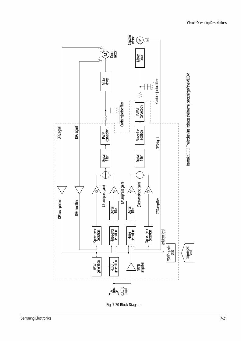
(2) Capstain Speed Error DetectorThe capstan speed control operates so as to hold the capstan at a constant rotational speed, by measuring the peri-od of the CFG signal. A digital counter detects the speed deviation from a preset value. The speed error data isadded to phase error data in a digital filter. this filter controls a pulse-width modulate (PWM) output, which con-trols the rotational speed and phase the captain. When the error is zero, the PWM circuit outputs a waveform with a 50% duty cycle.
The CFG input signal from the capstan motor is a square wave the CFG input signal is compared by a comparatorand than sent to speed error detector as the CFG signal.
The speed error detector uses the system clock to measure the period of the CFG signal, and detects the deviationfrom a preset data value. The preset data is the value that would result from measuring the CFG signal periodwith the clock signal if the capstan motor were running at the correct speed.
The error detector operates by latching a counter value when it detects an edge of the CFG signal.the latched counter provides 16 bits of speed error data for the digital filter to operate on. The digital filter adds the speed error data to phase error data from the capstan phase control system,then sendsthe result to the pulse-width modulator as capstan error data.
(3) Capstain Phase Error DetectorThe capstan phase error detector consists of a 16-bit counter, a capstan phase preset data register pair, a latch sig-nal circuit driven by a feedback signal, and a captain phase error data register pair.
The capstan phase control in rec mode is executed by comparing HD S/W, which is synchronized with V-sync,with devided CFG signal. And than it does in playback mode by comparing HD S/W, which is synchronized withDFG and DPG, with PB CTL signal.
The latch signal for the phase error data in record mode is the devied CFG signal, which is devided from the CFGsignal in the CFG frequency devider to a frequency of 30HZ. In playback, the latch signal is the devied CFG signal obtained by frequency division from the rising edge of PB-CTL signal (playback control pulse signal).
The error data is a signed binary value centered on a phase error of zero (corresponding to the correct rotationalphase). If the phase legs the correct phase ,the error is positive (+). If the phase leads the correct phase, the error is negative (-).
(4) Drum Speed Error DetectorDrum speed control operates so as to hold the drum at a constant rotational speed, by measuring the period ofthe DFG signal. A digital counter detects the speed deviation from a preset value. The speed error data is addedto phase error data in a digital filter. The filter controls a pulsewidth modulated (PWM) output,which controls therotational speed and phase of the drum.
The DFG input signal from the drum motor is a square wave. The DFG input signal is compared by a comparatorand than sent to the speed error detector as the DFG signal.
The speed error detector uses the system clock to measure the period of the DFG signal, and detects the deviationfrom a preset data value. The preset data is the value that would result from measuring the DFG signal periodwith the clock signal if the drum motor were running at the correct speed.
The error detector operates by latching a counter value when it detects an edge of the DFG signal. The latchedcount provides 16 bits of speed error data for the digital to operate on. The digital filter adds the speed error data to phase error data from the drum phase control system, then sendsthe result to the pulse-width modulator as drum error data.
Circuit Operating Descriptions
Samsung Electronics 7-23
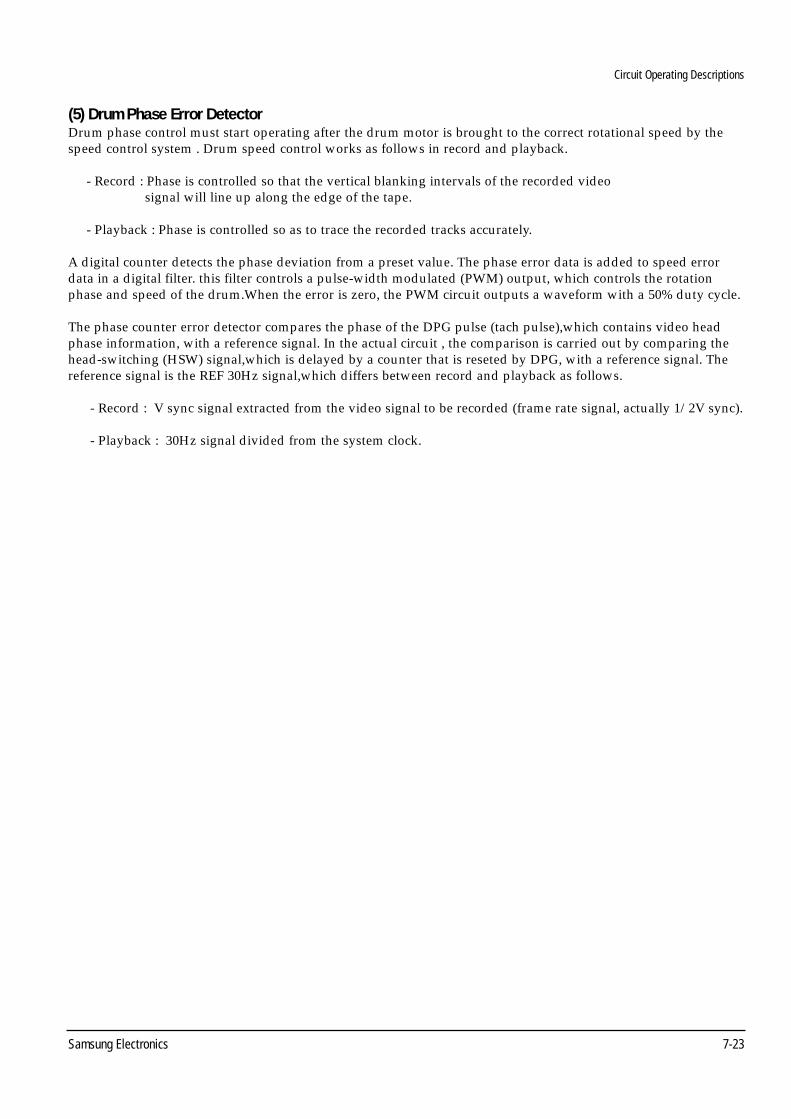
(5) Drum Phase Error DetectorDrum phase control must start operating after the drum motor is brought to the correct rotational speed by thespeed control system . Drum speed control works as follows in record and playback.
- Record : Phase is controlled so that the vertical blanking intervals of the recorded videosignal will line up along the edge of the tape.
- Playback : Phase is controlled so as to trace the recorded tracks accurately.
A digital counter detects the phase deviation from a preset value. The phase error data is added to speed errordata in a digital filter. this filter controls a pulse-width modulated (PWM) output, which controls the rotationphase and speed of the drum.When the error is zero, the PWM circuit outputs a waveform with a 50% duty cycle.
The phase counter error detector compares the phase of the DPG pulse (tach pulse),which contains video headphase information, with a reference signal. In the actual circuit , the comparison is carried out by comparing thehead-switching (HSW) signal,which is delayed by a counter that is reseted by DPG, with a reference signal. Thereference signal is the REF 30Hz signal,which differs between record and playback as follows.
- Record : V sync signal extracted from the video signal to be recorded (frame rate signal, actually 1/2V sync).
- Playback : 30Hz signal divided from the system clock.
Circuit Operating Descriptions
7-24 Samsung Electronics
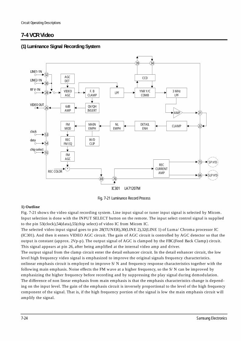
7-4 VCR Video
(1) Luminance Signal Recording System
Fig. 7-21 Luminance Record Process
LINE1-1N
IC301 LA71207M
LINE2-1N
RF V-1N
AGCDET
VIDEOAGC
F. BCLAMP
6dBAMP
QV/QHINSERT
LPF YNR Y/CCOMB
CCD
3 MHzLPF
AMP
32
30
28
69 70
clock
data
chip select
53
54
55
VIDEO OUT26
FMMOD
MAINEMPH
RECFM EQ
W/DCLIP
NLEMPH
DETAILENH
RECCURRENT
AMP
SP H'D
CLAMP
39 34
FMAGC
REC COLOR
22
21
66
73
+
SLP H'D
1) OutlineFig. 7-21 shows the video signal recording system. Line input signal or tuner input signal is selected by Micom.Input selection is done with the INPUT SELECT button on the remote. The input select control signal is suppliedto the pin 53(clock),54(data),55(chip select) of video IC from Micom IC. The selected video input signal goes to pin 28(TUNER),30(LINE 2),32(LINE 1) of Luma/Chroma processor IC(IC301). And then it enters VIDEO AGC circuit. The gain of AGC circuit is controlled by AGC detector so that theoutput is constant (approx. 2Vp-p). The output signal of AGC is clamped by the FBC(Feed Back Clamp) circuit.This signal appears at pin 26, after being amplified at the internal video amp and driver. The output signal from the clamp circuit enter the detail enhancer circuit. In the detail enhancer circuit, the lowlevel high frequency video signal is emphasized to improve the original signals frequency characteristics. onlinear emphasis circuit is employed to improve S/N and frequency response characteristics together with thefollowing main emphasis. Noise effects the FM wave at a higher frequency, so the S/N can be improved byemphasizing the higher frequency before recording and by suppressing the play signal during demodulation.The difference of non linear emphasis from main emphasis is that the emphasis characteristics change is depend-ing on the input level. The gain of the emphasis circuit is inversely proportional to the level of the high frequencycomponent of the signal. That is, if the high frequency portion of the signal is low the main emphasis circuit willamplify the signal.
Circuit Operating Descriptions
Samsung Electronics 7-25
2) Main Emphasis CircuitThe dynamically emphasized luminance signal is now supplied to the main emphasis circuit where all the highfrequency components of the signal are boosted more than the low frequency components. The boosting action isrequired for the high frequency components because in the FM recording method, the noise of the playback signalincreases in proportion to the modulated signal frequency or low level signal. By using the nonlinear emphasisand main emphasis system, the total S/N ratio is increased. The output of the main emphasis circuit is then supplied to the white and dark clip circuit.
3) White and Dark Clip CircuitAfter emphasis is performed, large overshoots and undershoots in the luminance signal are limited to a specifiedlevel. This is done to avoid FM over modulation. The output of the main emphasis circuit is then supplied to theFM modulator circuit.
4) FM ModulatorA. The amplitude of the FM signal is limited, so the signal is recorded on tape near the maximum
record level which increases the S/N ratio.B. The FM carrier is se to 3.4MHz (at the Sync tips) and the deviation to 4.4MHz by inside IC
circuit (for the white peak). The actual device which constitutes the FM modulator is a stable multivibrator. This multivibrator generates a sine wave output of variable frequency. The frequency of sine wave is governed by the level of the processed video signal at any given point. Therefore,the processed video signal varies the frequency of the sine wave which is frequency modulation (FM). Duringplayback in SLP mode, the crosstalk of the adjacent track is more apparent than is standard mode. It appears asjitter and noise on the monitor. To reduce this noise from the screen, the FM carrier frequency has to be 1/2fhshifted up during recording. This is done by applying the head switching pulse to the FM modulator controlpin57 during SLP recording. The FM modulated luminance signal goes to record equalizer circuit and it is mixedwith chrominance signal at the record Amp circuit inside video IC.
5) Record AmpThe frequency modulated luminance signal and chroma signal are mixed in the record amp of pre-amp blockinside video IC. Then this mixed signal is amplified and supplied to the video heads via the rotary transformerand recorded on the magnetic tape. Tape speed selection determines which video heads will be used. That is, signal output from pin 66 (SLP) and 73(SP) of pre-amp block are supplied to video heads. Control signal of speed mode is applied to pin 53(clock), 54(data), 55(chip select) of video IC from Micom IC.

Circuit Operating Descriptions
7-26 Samsung Electronics
91
IC301 LA71207M
74
9173
9172
9167
66
65
57
58
26
CH1 AMP
AMP
AMP
AMP
CH2
S PH'D
SLPH'D
CH2
CH1
H'D S/W
H'D AMP S/W
VIDEO OUT
FM AGC
NLDEEMPHA
YNR Y/CCOMB
PBFM-EQ
PB EQPHASE
DOUBLELIMIT
FMDEMOD
6dB AMP QV/QH F.BCLAMP Y/C MIX PICTURE
CTL
MA2NDE-EMPHA
SUBLPF
CLAMP
CCD
3MHZLPF
9121
9122
9134
9139NOISE
CANCELL
(2) Luminance Signal Playback System
Fig. 7-22 Luminance Playback Process
1) OutlineThe video signal recorded on the tape is picked up by CH1,CH2 head and is supplied to pre-amp block via rotarytrans. During playback, as per the speed, SP and SLP head is determined by Pin60 of respectively.CH1 signal inputs to Pins 65 and 74 while CH2 signal inputs to Pins 67 and 72 of video IC. The pick up operationis controlled by the head switching pulse inputted to pin 57. During the high portion of the switching pulse, CH2is picked-up and just the opposite is true for CH1. In the pre amp IC, the FM signal is amplified 60dB and this signal is applied to FM AGC.
2) FM AGC AMPAt the FM AGC Amp (FM), signals are automatically balanced. One of the AGC circuit outputs is fed to AGCdetector circuit which detects signal level fluctuations. The detector output signal is applied to the FM AGC Ampto keep the output constant.This output is applied to the PB FM EQ block. FM EQ is correct the phase distortionand level. The signal through PB EQ circuit is applied to the double limiter.
3) Double Limiter CircuitA FM signal on the tape which contains AM components will be read during playback. If there is a severe AMcomponent, a drastic drop in FM carrier can occur. This lack of FM carrier can be called a noise region. Doublelimiting is used for improving the S/N ratio and carrier loss. The playback FM signal is split into two paths, onegoes to high pass filler and sub-limiter. The other goes to the main-limiter after passing through a LPF. ONE pathof the FM signal goes to the high pass filter, so that the low frequency(AM) component can be removed, and theother carrier is supplied to the sub-limiter. The output signal of sub-limiter is mixed with the signal from the low-pass filter and sent to the FM demodulation circuit.

Circuit Operating Descriptions
Samsung Electronics 7-27
4) FM DEMODULATORThe FM demodulator consists of a stable mono multivibrator balanced modulator (BM) and a LPF. The FMdemodulator circuit first converts the FM signal to a pulse width modulator signal. Then the circuit smoothes thePWM signal to demodulate the video signal. This demodulated signal is fed to the LPF to remove its FM carriercomponent and any other harmonics. The demodulated luminance signal outputs from Pin 21 and is applied tothe 3MHz LPF through main deemphasis circuit. To reduce demodulation noise, the output of the 3MHz LPF isapplied to a non-linear deemphasis circuit through YNR circuit.
5) Main De-emphasis CircuitBefore modulation, main emphasis was performed. Because the high frequency components of video signal wereboosted more than the low frequency components in the recording mode, main deemphasis must be performed toobtain a normal video signal. That is this circuit returns the emphasized high frequency component to the originalvalue.
6) Non Linear De-Emphasis CircuitThis circuit is the counter part of the dynamic pre-emphasis circuit during recording. The characteristics are alsothe opposite of those in recording.
7) Drop Out Compensator/YNR CircuitThis circuit compensated for missing parts of the FM signal due to dust, dirt on the tape or irregular tape coating,etc. The clamped video signal is supplied to the CCD 1H circuit. The 1H delayed video signal from CCD block isalso supplied to the 6MHz LPF to reject the sampling noise of CCD IC.Then, the output of LPF is applied to Pin 34 of video IC. When the DOC detector detects the FM loss, a 1Hdelayed video signal is added in place of the missing signal.
8) Noise Canceller CircuitThe noise canceller circuit removes the high frequency noise contained in the video signal which has the reversecharacteristics of the detail enhance in the recording mode. The output of the noise canceller circuit is supplied tothe Luminance and Chrominance mixer circuit. The mixed chroma and luminance signal are then output at Pin26.
Circuit Operating Descriptions
7-28 Samsung Electronics
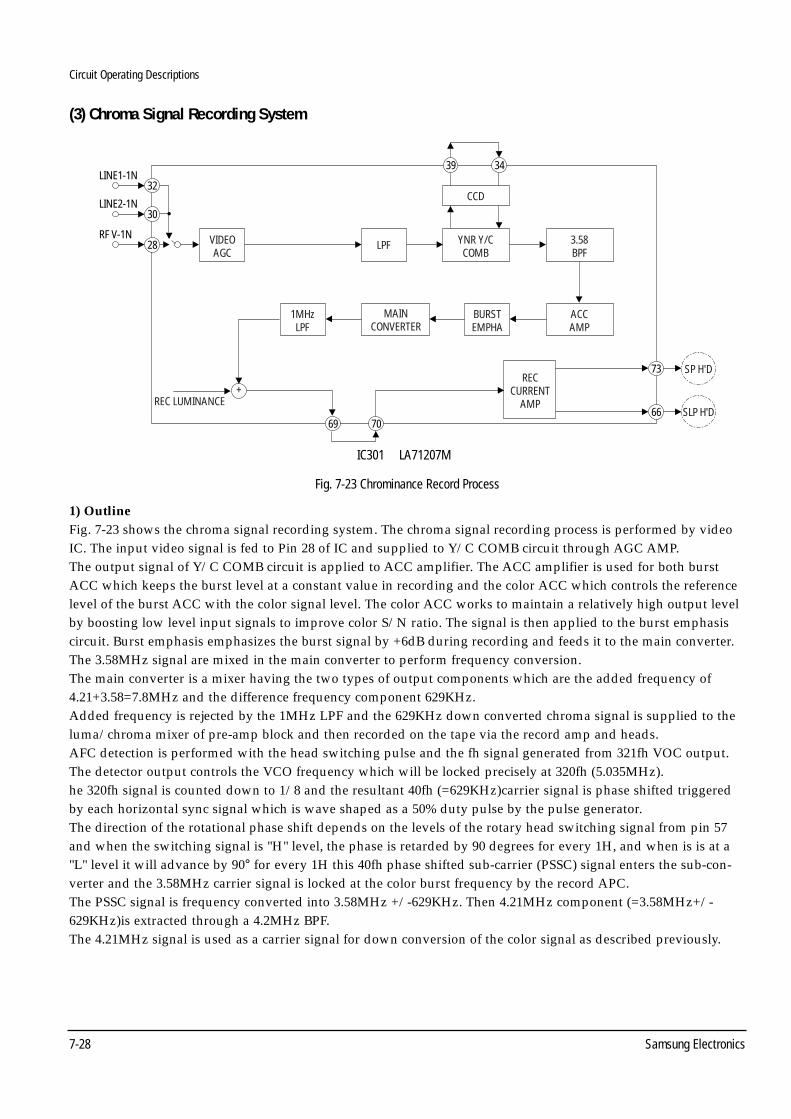
(3) Chroma Signal Recording System
Fig. 7-23 Chrominance Record Process
LINE1-1N
IC301 LA71207M
LINE2-1N
RF V-1N VIDEOAGC
LPF YNR Y/CCOMB
CCD
3.58BPF
32
30
28
69 70
RECCURRENT
AMP
SP H'D
1MHzLPF
MAINCONVERTER
BURSTEMPHA
ACCAMP
39 34
REC LUMINANCE66
73
+
SLP H'D
1) OutlineFig. 7-23 shows the chroma signal recording system. The chroma signal recording process is performed by videoIC. The input video signal is fed to Pin 28 of IC and supplied to Y/C COMB circuit through AGC AMP. The output signal of Y/C COMB circuit is applied to ACC amplifier. The ACC amplifier is used for both burstACC which keeps the burst level at a constant value in recording and the color ACC which controls the referencelevel of the burst ACC with the color signal level. The color ACC works to maintain a relatively high output levelby boosting low level input signals to improve color S/N ratio. The signal is then applied to the burst emphasiscircuit. Burst emphasis emphasizes the burst signal by +6dB during recording and feeds it to the main converter. The 3.58MHz signal are mixed in the main converter to perform frequency conversion.The main converter is a mixer having the two types of output components which are the added frequency of4.21+3.58=7.8MHz and the difference frequency component 629KHz.Added frequency is rejected by the 1MHz LPF and the 629KHz down converted chroma signal is supplied to theluma/chroma mixer of pre-amp block and then recorded on the tape via the record amp and heads. AFC detection is performed with the head switching pulse and the fh signal generated from 321fh VOC output.The detector output controls the VCO frequency which will be locked precisely at 320fh (5.035MHz).he 320fh signal is counted down to 1/8 and the resultant 40fh (=629KHz)carrier signal is phase shifted triggeredby each horizontal sync signal which is wave shaped as a 50% duty pulse by the pulse generator.The direction of the rotational phase shift depends on the levels of the rotary head switching signal from pin 57and when the switching signal is "H" level, the phase is retarded by 90 degrees for every 1H, and when is is at a"L" level it will advance by 90° for every 1H this 40fh phase shifted sub-carrier (PSSC) signal enters the sub-con-verter and the 3.58MHz carrier signal is locked at the color burst frequency by the record APC.The PSSC signal is frequency converted into 3.58MHz +/-629KHz. Then 4.21MHz component (=3.58MHz+/-629KHz)is extracted through a 4.2MHz BPF. The 4.21MHz signal is used as a carrier signal for down conversion of the color signal as described previously.

Circuit Operating Descriptions
Samsung Electronics 7-29
2) ACC (Automatic Color Gain Control) CircuitThe ACC is used as burst ACC in the LP mode, however it is also used for peak ACC in the SP/SLP mode. The purpose of using two different ACC operations is to improve the overall Chroma S/N ratio during playback.In SP and SLP, there is H-sync alignment. This indicates that there is bust alignment as well. Whenever two videotracks overlap or a video head picks up crosstalk from an adjacent track, beats are produced during playback.Perhaps the most noticeable beats are produced by H-sync and burst. But in SP and SLP, these beats occur right atH-sync and burst and are out of the picture. In LP, however, there is no H-sync alignment and these beats can beseen in the picture. To keep the beats at a minimum in LP, we keep the burst level constant so that the beat inten-sity is constant. We know that ACC acts to improve the color S/N,and in LP, the ACC detector locks at the burstlevel,and keeps it constant. Thus we have ACC operation with the least beats. In SP and SLP, the beats caused byburst overlap are out of picture, so we don't really mind if the burst level changes or not. To improve the colorS/N ratio even more,we use peak ACC in SP and SLP.That is,if the chroma level is too low to record, the amplifi-cation degree is increased by 3dB. However, the chroma level is sufficient for recording, this peak ACC is changedto burst ACC to avoid over amplification. By changing the ACC according to picture color content, the burst levelmay vary. The color ratio improvement is based on the color content itself during SP and SLP provides a some-what better S/N ratio.
3) Four (4) Phase RotationCH1 is advanced 90° every channel, while CH2 is delayed 90°. When the frequency is set to 629KHz, if phase isshifted by +/-90 it becomes 629KHz +/-90. The 40fh+/-90 (=629KHz +/-90)is balanced modulated via fsc(3.58MHz) depending on which side band is detected. That is, the fs +40fh+/-90 (4.2MHz +/-90) of total frequen-cy is supplied to the main converter. In record mode, the signal operates same as in play back mode. During play-back, the phase is returned to original state.
4) AFC (Automatic Frequency Control) CircuitLuminance signal is input to H-sync separator. The H-sync is separated and supplied to phase comparator.This signal can be described as fh (Horizontal Sync frequency of input video signal). However, VCO oscillates at320fh (5.035MHz). This 321fh is counted down by 1/8 and 1/40 and resultant fh is supplied to phase comparator.fh and fh are supplied to the phase comparator for comparison of their phases. After comparison, the phase differences is output to VCO (320fh) in terms of error voltage. Therefore, the oscillation frequency of VCO is controlled by this error voltage. That is, if the fh phase is changed by H-sync signal fh, error voltage is changedaccordingly and if the phases of fh and fh are met due to change of VCO oscillation frequency, error voltage doesnot feedback. 320fh VCO is oscillated in accordance with phase sync at fh. Therefore, 40fh input to sub converterby phase shift is always sync horized with phase. The AFC loop performs the same operation during record and playback. In recording, phase of VCO is in accor-dance with H-sync signal of current video signal. Which in playback, the phase sync of VCO is consistent with H-sync signal which is separated from the video signal.
Circuit Operating Descriptions
7-30 Samsung Electronics
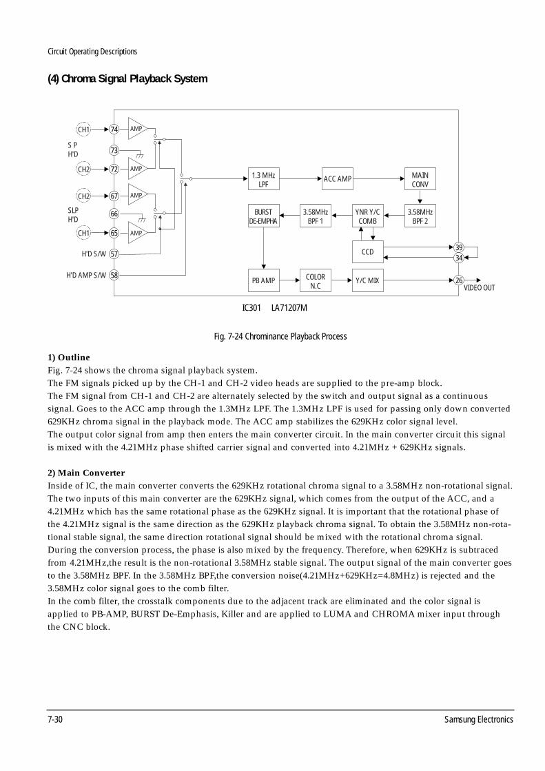
(4) Chroma Signal Playback System
Fig. 7-24 Chrominance Playback Process
IC301 LA71207M
9174
9173
9172
9167
66
65
57
58
CH1 AMP
AMP
AMP
AMP
CH2
S PH'D
SLPH'D
CH2
CH1
H'D S/W
H'D AMP S/W
1.3 MHzLPF
ACC AMP MAINCONV
BURSTDE-EMPHA
3.58MHzBPF 1
YNR Y/CCOMB
PB AMP COLORN.C
Y/C MIX
3.58MHzBPF 2
CCD
9126
3934
VIDEO OUT
1) OutlineFig. 7-24 shows the chroma signal playback system.The FM signals picked up by the CH-1 and CH-2 video heads are supplied to the pre-amp block.The FM signal from CH-1 and CH-2 are alternately selected by the switch and output signal as a continuous signal. Goes to the ACC amp through the 1.3MHz LPF. The 1.3MHz LPF is used for passing only down converted629KHz chroma signal in the playback mode. The ACC amp stabilizes the 629KHz color signal level. The output color signal from amp then enters the main converter circuit. In the main converter circuit this signalis mixed with the 4.21MHz phase shifted carrier signal and converted into 4.21MHz + 629KHz signals.
2) Main ConverterInside of IC, the main converter converts the 629KHz rotational chroma signal to a 3.58MHz non-rotational signal.The two inputs of this main converter are the 629KHz signal, which comes from the output of the ACC, and a4.21MHz which has the same rotational phase as the 629KHz signal. It is important that the rotational phase ofthe 4.21MHz signal is the same direction as the 629KHz playback chroma signal. To obtain the 3.58MHz non-rota-tional stable signal, the same direction rotational signal should be mixed with the rotational chroma signal.During the conversion process, the phase is also mixed by the frequency. Therefore, when 629KHz is subtracedfrom 4.21MHz,the result is the non-rotational 3.58MHz stable signal. The output signal of the main converter goesto the 3.58MHz BPF. In the 3.58MHz BPF,the conversion noise(4.21MHz+629KHz=4.8MHz) is rejected and the3.58MHz color signal goes to the comb filter.In the comb filter, the crosstalk components due to the adjacent track are eliminated and the color signal isapplied to PB-AMP, BURST De-Emphasis, Killer and are applied to LUMA and CHROMA mixer input throughthe CNC block.
Circuit Operating Descriptions
Samsung Electronics 7-31
BPF MAINCONV ( - )
SUBCONV ( + )
LPFVIDEO IN
fs = 3.58MHz
320fh = 5.03MHzfh = 15.734 KHz
fs = 3.579545MHz
40th = 629KHz
fs + 40th = 3.58MHz + 0.62MHz = 4.2MHz
40th = 629KHz
REC OUT
X’TALOSC
fs
BPF
fh
1/8D/C
VC0320fh
LPF MAINCONV ( - )
SUBCONV ( + )
BPFPB COLOR IN
fs = 3.58MHz
320fh = 5.03MHzfh = 15.734 KHz
fs = 3.579545MHz
40th = 629KHz
fs + 40th = 3.58MHz + 0.62MHz = 4.2MHz
40th = 629KHz
PB OUT
X’TALOSC
fs
BPF
fh
1/8D/C
VC0320fh
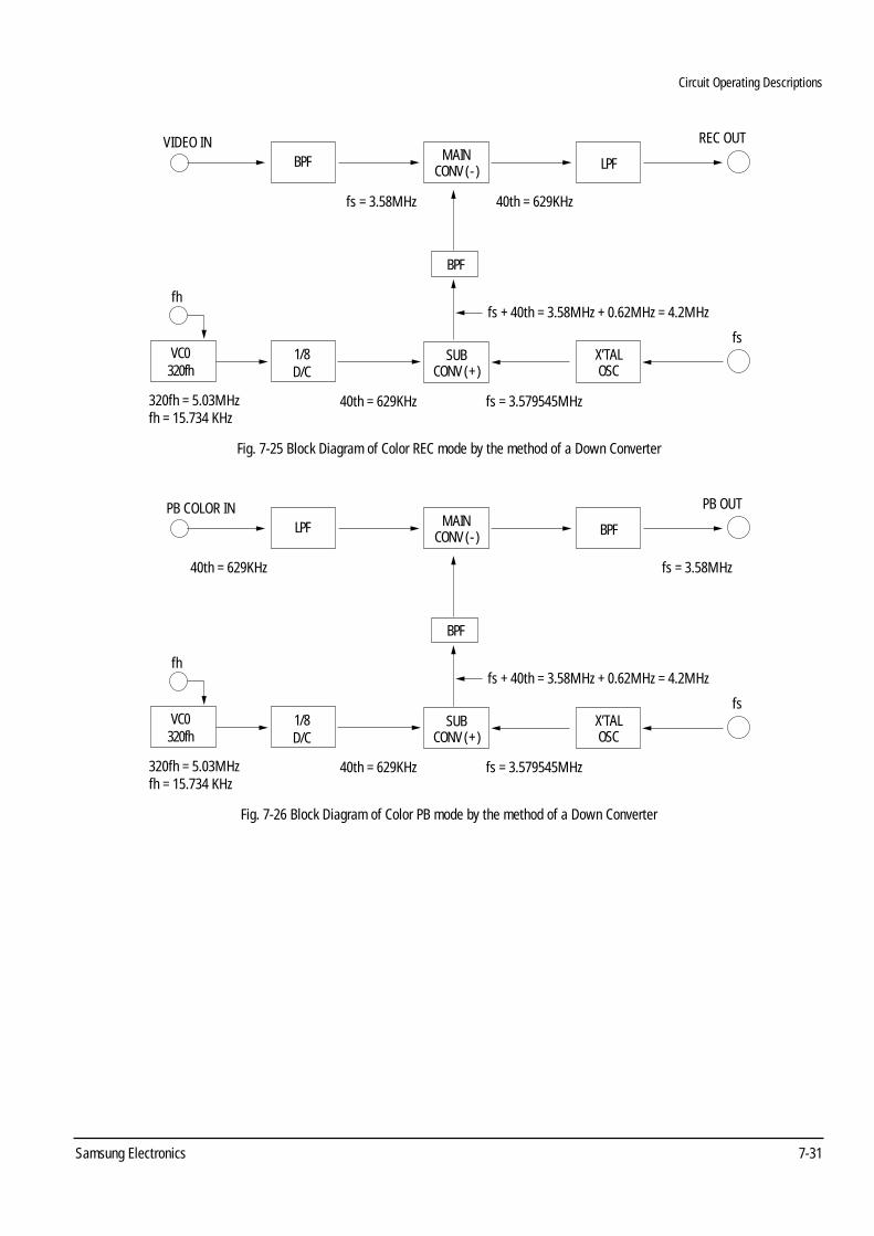
Fig. 7-25 Block Diagram of Color REC mode by the method of a Down Converter
Fig. 7-26 Block Diagram of Color PB mode by the method of a Down Converter
Circuit Operating Descriptions
7-32 Samsung Electronics
7-5 Hi-Fi Audio
(1) Outline
Hi-Fi circuit consists of HiFi audio LPF,VCO,BPF,FM detect circuit and switching noise compensator, PRE-AMP etc. Linear
audio consists of an ALC circuit,REC EQ circuit and a PB EQ circuit.
Hi-Fi and Linear audio share the same input selector,output selector and mute circuit.
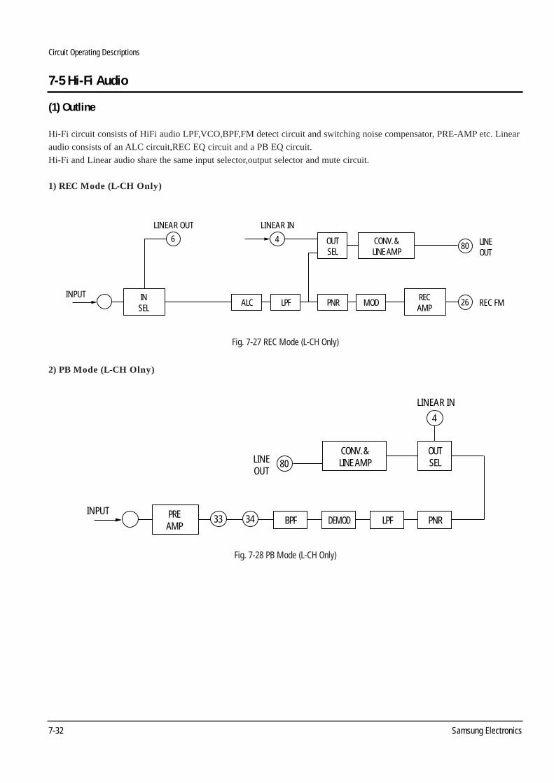
1) REC Mode (L-CH Only)
INSEL
RECAMP
INPUTALC LPF PNR MOD 26 REC FM
OUTSEL
CONV. &LINE AMP
80 LINEOUT
LINEAR INLINEAR OUT
46
PREAMP
INPUT33 34 BPF DEMOD LPF PNR
CONV. &LINE AMP80
LINEAR IN
OUTSEL
4
LINEOUT
Fig. 7-27 REC Mode (L-CH Only)
Fig. 7-28 PB Mode (L-CH Only)
2) PB Mode (L-CH Olny)
Circuit Operating Descriptions
Samsung Electronics 7-33
(2) Block Description
1) Input SelectorInput selector outputs 1 signal from 4 different signals received. It outputs 1 selected signal from tuner,rear,front.
2) Normal(Linear) SelectorTwo signals,L-CH and R-CH are inputed to Hi-Fi IC.But,linear audio is capable of receiving only one signal.Therefore,the
2 input signals must be selected. Usually,the outputs are mixed signals of L-CH and R-CH unlike the input selector,the
normal selector does not amplify the selected signal.
3) Output SelectorIt selects to output Hi-Fi L-CH,Hi-Fi R-CH,LINEAR and MIX(Hi-Fi+LINEAR) signals with the final output IC
pin 78 (R-CH) and pin 80 (L-CH).
4) Output ALC(Convertor)ALC is used because when the input level of RF converter gets bigger,it shows up as noise on the screen. But,this block is
not used this model(ALC OFF)
5) PNR(Peak Noise Reduction)It is a type of emphasis,de-emphasis function to eliminate noise during modulation /demodulation PNR operates as that of
VHS FORMAT to reduce noise.
6) Audio LimiterBefore modulating the signals from PNR block,it limits signals exceeding the size limit to max deviation of +/- 150KHz.
7) VCO(Voltage Control Oscillation)It is a modulation functionthat oscillates 1.3MHz (L-CH) and 1.7MHz (R-CH).
8) RF LPFIt is a function to eliminate the harmonic components of Hi-Fi carrier formed during VCO,which may affect other block.
It’s pass-band approximately 2MHz.
9) MIXERIt mixes the Hi-Fi carrier formed in L-CH and R-CH. However,due to the frequency difference between L-CH and
R-CH,when equal amount of R-CH is recorded to tape,R-CH is must smaiier than L-CH.
Therefore,the R-CH output is approximately 10dB bigger than L-CH.
10) Current AmpIt is the final amplifier of the mixed Hi-Fi carrier IC pin 28’s resistance controls current, which change the size of IC
pin 26.
11) AGC(Auto Gain Control)It maintains uniform size of Hi-Fi envelope,which is inputed by pre-amp in play back mode.
12) BPF(Band Pass Filter)L-CH and R-CH each has BPF. The center frequency is same as carrier frequency.
It is used to receive only Hi-Fi carrier from all signals inputed to pre-amp.
Circuit Operating Descriptions
7-34 Samsung Electronics
13) SW Noise CompensationUnlike the linear audio,insted of using fixed head,drum heads are used,which creates halting points However,in order for
the audio to be headed continuously,the damages from halting points are modulated,which creates noise. SW noise
compensation is a block to minimize this particular noise.
14) Hold PulseIt makes standard signal(Pulse) to compensate SW noise.
15) DET(Hi-Fi/LINEAR)From the Hi-Fi envelope inputed from pre-amp,it decides whether the signal passing through L-CH BPF is Hi-Fi or
LINEAR tape it’s size(the signal passing through BPF is below 10mVpp, it is not Hi-Fi,therefore,it output linear)
16) DOC(Drop Out Compensation)If demodulation is conducted without properly treating the damage on Hi-Fi envelope caused by scratch on the tape,noise
occurs. In order to improve this noise occurrence,DO DET compensate the drop-out using the same methode of
compensating the switching noise when the damage on the envelope ranges 10~15mVpp.
17) ENV DETTo obtain optimal tracking,envelop must be peak to peak and micom should be in DC. It is a function to convert Hi-Fi
envelop to DC. If it is lower than 0.8V at micom,it sends linear mode date to HiFi IC.
18) Serial Data DecoderIt receives IIC BUS to enable the operation of inner block and decodes into serial data.
Circuit Operating Descriptions
Samsung Electronics 7-35
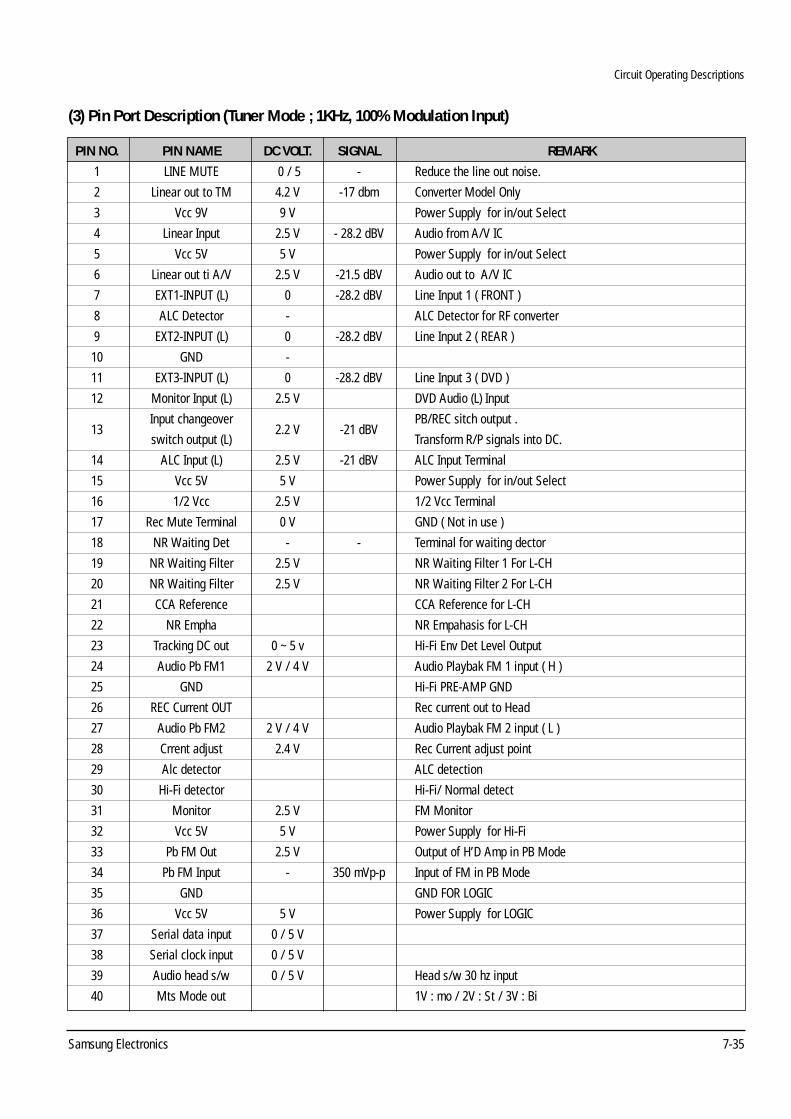
(3) Pin Port Description (Tuner Mode ; 1KHz, 100% Modulation Input)
PIN NO. PIN NAME DC VOLT. SIGNAL REMARK
1 LINE MUTE 0 / 5 - Reduce the line out noise.
2 Linear out to TM 4.2 V -17 dbm Converter Model Only
3 Vcc 9V 9 V Power Supply for in/out Select
4 Linear Input 2.5 V - 28.2 dBV Audio from A/V IC
5 Vcc 5V 5 V Power Supply for in/out Select
6 Linear out ti A/V 2.5 V -21.5 dBV Audio out to A/V IC
7 EXT1-INPUT (L) 0 -28.2 dBV Line Input 1 ( FRONT )
8 ALC Detector - ALC Detector for RF converter
9 EXT2-INPUT (L) 0 -28.2 dBV Line Input 2 ( REAR )
10 GND -
11 EXT3-INPUT (L) 0 -28.2 dBV Line Input 3 ( DVD )
12 Monitor Input (L) 2.5 V DVD Audio (L) Input
13Input changeover
2.2 V -21 dBVPB/REC sitch output .
switch output (L) Transform R/P signals into DC.
14 ALC Input (L) 2.5 V -21 dBV ALC Input Terminal
15 Vcc 5V 5 V Power Supply for in/out Select
16 1/2 Vcc 2.5 V 1/2 Vcc Terminal
17 Rec Mute Terminal 0 V GND ( Not in use )
18 NR Waiting Det - - Terminal for waiting dector
19 NR Waiting Filter 2.5 V NR Waiting Filter 1 For L-CH
20 NR Waiting Filter 2.5 V NR Waiting Filter 2 For L-CH
21 CCA Reference CCA Reference for L-CH
22 NR Empha NR Empahasis for L-CH
23 Tracking DC out 0 ~ 5 v Hi-Fi Env Det Level Output
24 Audio Pb FM1 2 V / 4 V Audio Playbak FM 1 input ( H )
25 GND Hi-Fi PRE-AMP GND
26 REC Current OUT Rec current out to Head
27 Audio Pb FM2 2 V / 4 V Audio Playbak FM 2 input ( L )
28 Crrent adjust 2.4 V Rec Current adjust point
29 Alc detector ALC detection
30 Hi-Fi detector Hi-Fi/ Normal detect
31 Monitor 2.5 V FM Monitor
32 Vcc 5V 5 V Power Supply for Hi-Fi
33 Pb FM Out 2.5 V Output of H’D Amp in PB Mode
34 Pb FM Input - 350 mVp-p Input of FM in PB Mode
35 GND GND FOR LOGIC
36 Vcc 5V 5 V Power Supply for LOGIC
37 Serial data input 0 / 5 V
38 Serial clock input 0 / 5 V
39 Audio head s/w 0 / 5 V Head s/w 30 hz input
40 Mts Mode out 1V : mo / 2V : St / 3V : Bi
Circuit Operating Descriptions
7-36 Samsung Electronics
PIN NO. PIN NAME DC VOLT. SIGNAL REMARK
41 CCA Reference CCA Reference for R-CH
42 NR Empha NR Empahasis for R-CH
43 NR Waiting Filter 2.5 V NR Waiting Filter 2 For R-CH
44 NR Waiting Filter 2.5 V NR Waiting Filter 1 For R-CH
45 NR Waiting Det - - Terminal for waiting dector
46 Vcc 5V 5 V Power Supply for in/out Select
47 ALC Input (R) 2.5 V -21 dBV ALC Input Terminal
48Input changeover
2.2 V -21 dBVPB/REC sitch output .
switch output (R) Transform R/P signals into DC.
49 Mute Control
50 GND GND FOR ANALOGE
51 FSC IN 200 mVp-p 3.58 Mhz input
52 DC Reg 1.2 V Bandgap Power supply for MTS
53 Stereo PLL filter 3.8 V LPF for Stereo PLL
54 Vcc 5V 5 V Power Supply for MTS Select
55 Pilot Canceller f 3.8 V CTL Pin of cancel signal for pilot C.
56 FM Filter Filter for making stable dc
57 SIF Input SIF Audio input from TM Block
58 REG Filter 4.5 V Filter of reference voltage source.
59 Filter Auto Adjust 3.8 V Loof filterof PLL for auto adj
60 Pilot Det Filter 3.8 V Detection for pilot detection circuit
61 PC_DC_MO 3.3 V Absorbing the DC offset
62 PCDOUT 3.8 V Absorbing the DC offset
63 PCDIN 3.8 V Absorbing the DC offset
64 PCDBXIN 2.6 V Absorbing the DC offset
65 Main V/I convert 3.8 V Converting the voltage of signal
66 SPE Det V/I convert 3.8 V Connecting pin of smooth capacity of detection circuit.
67 Spectral DET Converting the voltage of signal
68 Wide Band Det Connecting pin of smooth capacity of detection circuit.
69 EXT1-INPUT (R) 0 -28.2 dBV Line Input 1 ( FRONT )
70 GND GND FOR MTS
71 EXT2-INPUT (R) 0 -28.2 dBV Line Input 2 ( REAR )
72 Wid det V/I convert 3.8 V Converting the voltage of signal
73 EXT3-INPUT (R) 0 -28.2 dBV Line Input 3 ( DVD )
74 Monitor Input (R) 2.5 V DVD Audio (R) Input
75 PCDCOSPE Absorbing the DC offset
76 PC_OUT_DBX 3.3 V Absorbing the DC offset
77 LINE MUTE ( R ) 0 / 5 - Reduce the line out noise.
78 Line out (R-CH)
79 GND GND FOR AUDIO
80 Line out (L-CH)
Circuit Operating Descriptions
Samsung Electronics 7-37
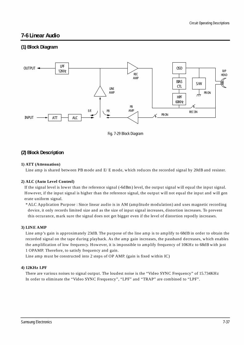
7-6 Linear Audio
(1) Block Diagram
INPUT ATT ALC
LPF12KHz
OUTPUT OSD
BIASCTL
HPF60KHz
S/W
PB ON
REC ONPB ON
PBAMP
RECAMP
LINEAMP
E/E PB
R/PHEAD
Fig. 7-29 Block Diagram
(2) Block Description
1) ATT (Attenuation)Line amp is shared between PB mode and E/E mode, which reduces the recorded signal by 20dB and resister.
2) ALC (Auto Level Control)If the signal level is lower than the reference signal (-6dBm) level, the output signal will equal the input signal. However, if the input signal is higher than the reference signal, the output will not equal the input and will generate uniform signal.* ALC Application Purpose : Since linear audio is in AM (amplitude modulation) and uses magnetic recording
device, it only records limited size and as the size of input signal increases, distortion increases. To prevent this occurance, mark sure the signal does not get bigger even if the level of distortion repodly increases.
3) LINE AMPLine amp’s gain is approximately 23dB. The purpose of the line amp is to amplify to 68dB in order to obtain the recorded signal on the tape during playback. As the amp gain increases, the passband decreases, which enables the amplification of low frequency. However, it is impossible to amplify frequency of 10KHz to 68dB with just 1 OPAMP. Therefore, to satisfy frequency and gain. Line amp must be constructed into 2 steps of OP AMP. (gain is fixed within IC)
4) 12KHz LPFThere are various noises to signal output. The loudest noise is the “Video SYNC Frequency” of 15.734KHz In order to eliminate the “Video SYNC Frequency”, “LPF” and “TRAP” are combined to “LPF”.
Circuit Operating Descriptions
7-38 Samsung Electronics
5) PB AMP
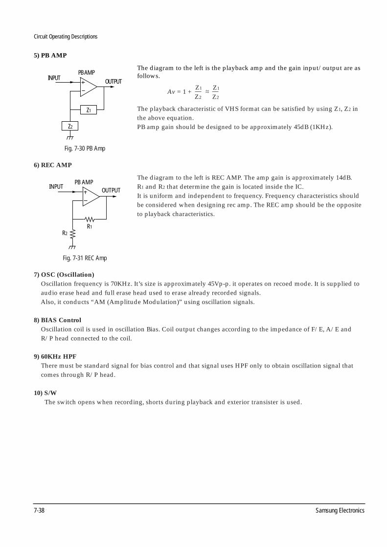
The diagram to the left is the playback amp and the gain input/output are asfollows.
Av = 1 +
The playback characteristic of VHS format can be satisfied by using Z1, Z2 inthe above equation. PB amp gain should be designed to be approximately 45dB (1KHz).
Z1
Z2
INPUTPB AMP
OUTPUT
Fig. 7-30 PB Amp
Z2
Z1
Z2
Z1~~
6) REC AMP
The diagram to the left is REC AMP. The amp gain is approximately 14dB. R1 and R2 that determine the gain is located inside the IC. It is uniform and independent to frequency. Frequency characteristics shouldbe considered when designing rec amp. The REC amp should be the oppositeto playback characteristics.
OUTPUTPB AMP
INPUT
R1R2
Fig. 7-31 REC Amp
7) OSC (Oscillation)Oscillation frequency is 70KHz. It’s size is approximately 45Vp-p. it operates on recoed mode. It is supplied to audio erase head and full erase head used to erase already recorded signals.Also, it conducts “AM (Amplitude Modulation)” using oscillation signals.
8) BIAS ControlOscillation coil is used in oscillation Bias. Coil output changes according to the impedance of F/E, A/E and R/P head connected to the coil.
9) 60KHz HPFThere must be standard signal for bias control and that signal uses HPF only to obtain oscillation signal that comes through R/P head.
10) S/WThe switch opens when recording, shorts during playback and exterior transister is used.
Circuit Operating Descriptions
Samsung Electronics 7-39
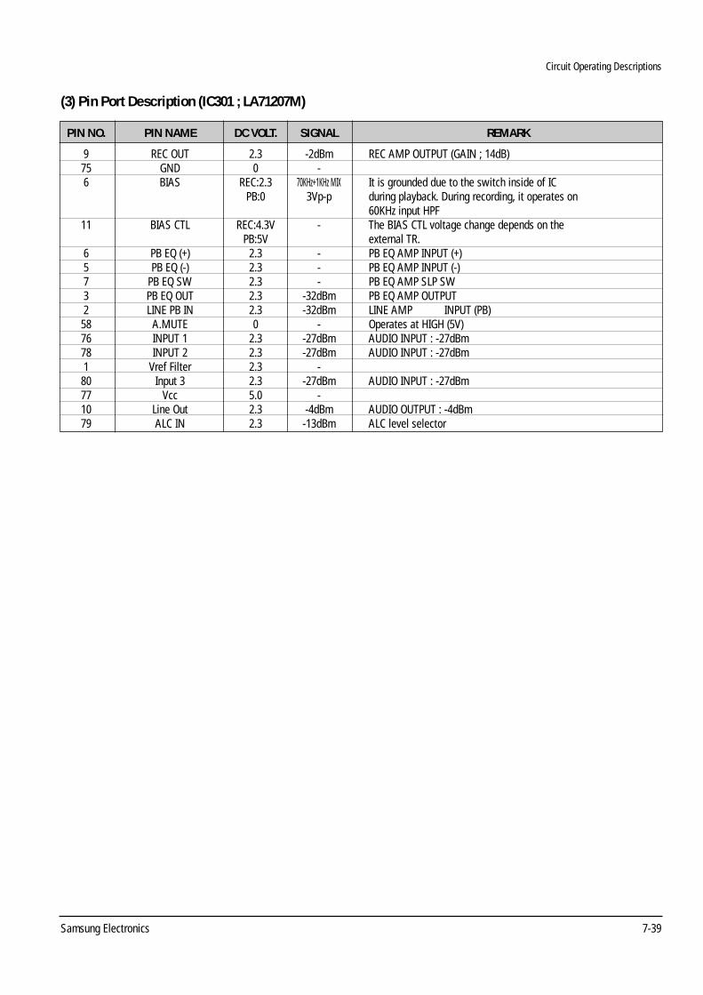
(3) Pin Port Description (IC301 ; LA71207M)
PIN NO. PIN NAME DC VOLT. SIGNAL REMARK
9 REC OUT 2.3 -2dBm REC AMP OUTPUT (GAIN ; 14dB)75 GND 0 -6 BIAS REC:2.3 70KHz+1KHz MIX It is grounded due to the switch inside of IC
PB:0 3Vp-p during playback. During recording, it operates on60KHz input HPF
11 BIAS CTL REC:4.3V - The BIAS CTL voltage change depends on the PB:5V external TR.
6 PB EQ (+) 2.3 - PB EQ AMP INPUT (+)5 PB EQ (-) 2.3 - PB EQ AMP INPUT (-)7 PB EQ SW 2.3 - PB EQ AMP SLP SW3 PB EQ OUT 2.3 -32dBm PB EQ AMP OUTPUT2 LINE PB IN 2.3 -32dBm LINE AMP INPUT (PB)
58 A.MUTE 0 - Operates at HIGH (5V)76 INPUT 1 2.3 -27dBm AUDIO INPUT : -27dBm78 INPUT 2 2.3 -27dBm AUDIO INPUT : -27dBm1 Vref Filter 2.3 -
80 Input 3 2.3 -27dBm AUDIO INPUT : -27dBm77 Vcc 5.0 -10 Line Out 2.3 -4dBm AUDIO OUTPUT : -4dBm79 ALC IN 2.3 -13dBm ALC level selector
Circuit Operating Descriptions
7-40 Samsung Electronics
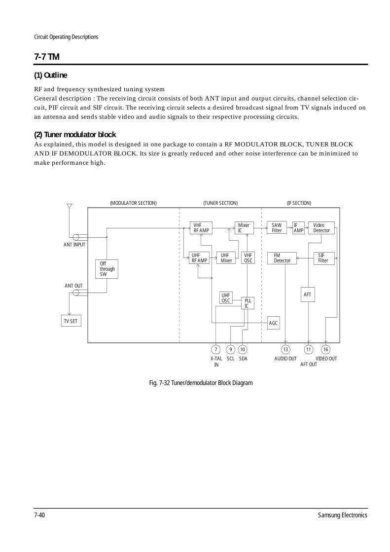
RF and frequency synthesized tuning systemGeneral description : The receiving circuit consists of both ANT input and output circuits, channel selection cir-cuit, PIF circuit and SIF circuit. The receiving circuit selects a desired broadcast signal from TV signals induced onan antenna and sends stable video and audio signals to their respective processing circuits.
(2) Tuner modulator blockAs explained, this model is designed in one package to contain a RF MODULATOR BLOCK, TUNER BLOCKAND IF DEMODULATOR BLOCK. Its size is greatly reduced and other noise interference can be minimized tomake performance high.
Fig. 7-32 Tuner/demodulator Block Diagram
ANT INPUT
(MODULATOR SECTION) (TUNER SECTION) (IF SECTION)
ANT OUT
OffthroughSW
VHFRF AMP
UHFRF AMP
UHFMixer
VHFOSC
FMDetector
SIFFilter
UHFOSC PLL
IC
AGC
AFT
MixerIC
SAWFilter
IFAMP
VideoDetector
TV SET
SCLX-TALIN
SDA AUDIO OUTAFT OUT
VIDEO OUT
97 10 13 11 16
7-7 TM
(1) Outline

Circuit Operating Descriptions
Samsung Electronics 7-41
(3) Tuner BlockA. Low pass filter & high pass filterThis consists of IF trap circuit and UHF & VHF separation circuit. If the input signal is IF(45.75MHz), this filterprevents interference.
B. Single tune & RF AMPThis consists of a filter circuit, RF AMP, impedance conversion circuit, image trap and a single tuning circuit. Itprevents noise and other interference signals. RF AMP is controlled by AGC come from IF DEMOD block.
C. Double tuneIt consists of a double tuning circuit to improve rejection characteristic which results in a better band characteris-tic.
D. MOP IC (Mixer, OSC, PLL)It consists a VHS and UHF OSC and mixer circuit. We applied a double balance mixer to have better rejectioncharacteristic, it shows especially various beat characteristic. It serects channels and contains charge pump band driver. The minimum step standard frequency 31.25KHZ.
AGCfrom IF Section
Prescaler
REF
C.P.LPF
Tu voltageout
Fsc IN Tu Clock Data +B
IFto IF Section
VLVHU
BAND SW
MOP ICCXA3250AN (SONY)SN761672A (TEXAS Instruments)
MOP IC! SONY : CSA3250AN@ T I : SN761672A
FROMMD SECTION
L.P.F
H.P.F
S.T(VL)
S.T(U)
S.T(VL) D.T(VL)
V.MIX
VHFOSD
UHFOSD
OSCAMP
IFAMP
U.MIX IF S.T
D.T(VH)
D.T(U)
V.RF Amp
U.RF Amp
H.P.F+
IF trap
Fig. 7-33 Tuner Section Block Diagram
Circuit Operating Descriptions
7-42 Samsung Electronics
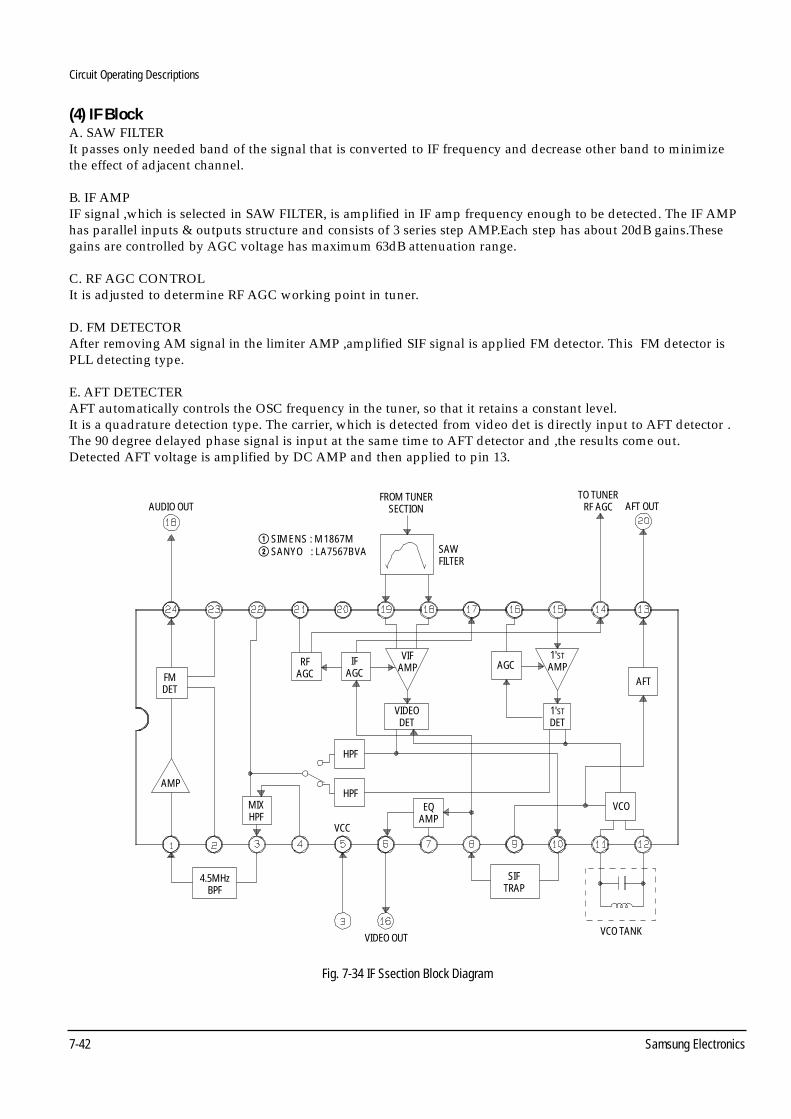
(4) IF BlockA. SAW FILTERIt passes only needed band of the signal that is converted to IF frequency and decrease other band to minimizethe effect of adjacent channel.
B. IF AMPIF signal ,which is selected in SAW FILTER, is amplified in IF amp frequency enough to be detected. The IF AMPhas parallel inputs & outputs structure and consists of 3 series step AMP.Each step has about 20dB gains.Thesegains are controlled by AGC voltage has maximum 63dB attenuation range.
C. RF AGC CONTROLIt is adjusted to determine RF AGC working point in tuner.
D. FM DETECTOR After removing AM signal in the limiter AMP ,amplified SIF signal is applied FM detector. This FM detector isPLL detecting type.
E. AFT DETECTERAFT automatically controls the OSC frequency in the tuner, so that it retains a constant level.It is a quadrature detection type. The carrier, which is detected from video det is directly input to AFT detector .The 90 degree delayed phase signal is input at the same time to AFT detector and ,the results come out.Detected AFT voltage is amplified by DC AMP and then applied to pin 13.
! SIMENS : M1867M@ SANYO : LA7567BVA
AUDIO OUTFROM TUNER
SECTION
SAWFILTER
FMDET
RFAGC
IFAGC
VIFAMP
VIDEODET
AGC1'STAMP
1'STDET
AFT
VCO
HPF
HPFMIXHPF
4.5MHzBPF
VIDEO OUT
SIFTRAP
VCO TANK
VCC
EQAMP
AMP
TO TUNERRF AGC AFT OUT
Fig. 7-34 IF Ssection Block Diagram
Circuit Operating Descriptions
Samsung Electronics 7-43
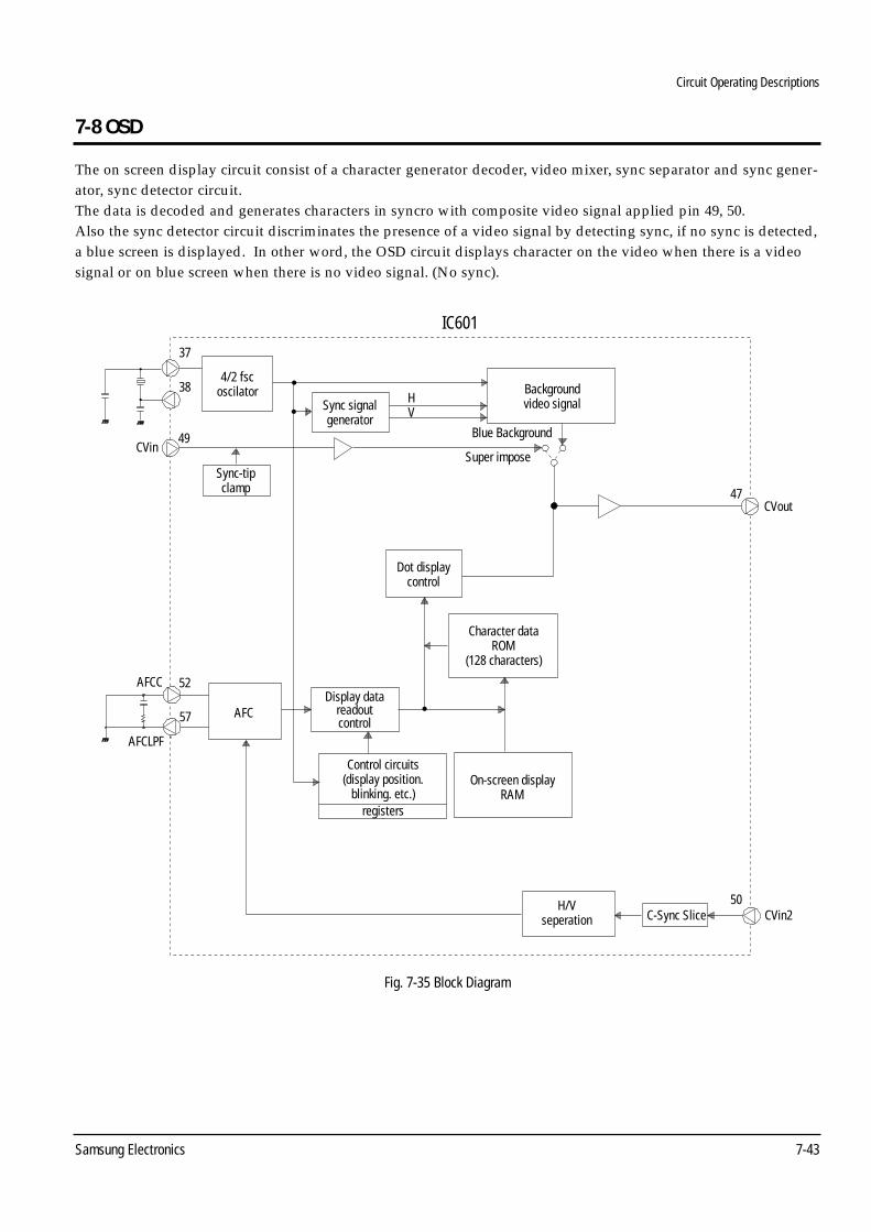
7-8 OSD
The on screen display circuit consist of a character generator decoder, video mixer, sync separator and sync gener-ator, sync detector circuit.The data is decoded and generates characters in syncro with composite video signal applied pin 49, 50.Also the sync detector circuit discriminates the presence of a video signal by detecting sync, if no sync is detected,a blue screen is displayed. In other word, the OSD circuit displays character on the video when there is a videosignal or on blue screen when there is no video signal. (No sync).
49CVin
4/2 fscoscilator
Sync signalgenerator
HBackgroundvideo signal
CVout
Blue Background
Super impose
IC601
Dot displaycontrol
Character dataROM
(128 characters)
Control circuits(display position.
blinking. etc.)registers
On-screen displayRAM
H/Vseperation
Display datareadoutcontrol
AFC
V
Sync-tipclamp
38
37
52
57
CVin2
47
50C-Sync Slice
AFCC
AFCLPF
Fig. 7-35 Block Diagram
Circuit Operating Descriptions
7-44 Samsung Electronics
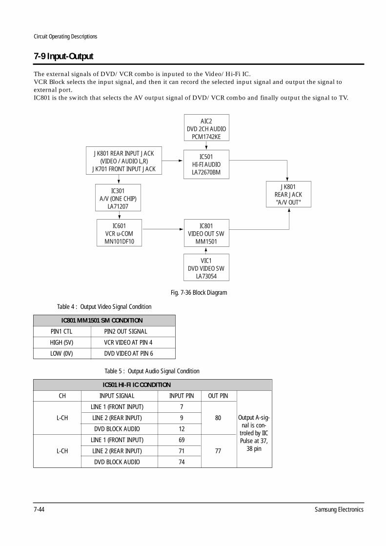
7-9 Input-Output
The external signals of DVD/VCR combo is inputed to the Video/Hi-Fi IC.VCR Block selects the input signal, and then it can record the selected input signal and output the signal toexternal port.IC801 is the switch that selects the AV output signal of DVD/VCR combo and finally output the signal to TV.
VIC1DVD VIDEO SW
LA73054
IC801VIDEO OUT SW
MM1501
JK801REAR JACK"A/V OUT"
AIC2DVD 2CH AUDIO
PCM1742KE
IC501HI-FI AUDIOLA72670BM
IC301A/V (ONE CHIP)
LA71207
JK801 REAR INPUT JACK(VIDEO / AUDIO L,R)
JK701 FRONT INPUT JACK
IC601VCR u-COMMN101DF10
Fig. 7-36 Block Diagram
Table 5 : Output Audio Signal Condition
IC501 HI-FI IC CONDITION
CH INPUT SIGNAL INPUT PIN OUT PIN
LINE 1 (FRONT INPUT) 7
L-CH LINE 2 (REAR INPUT) 9 80
DVD BLOCK AUDIO 12
LINE 1 (FRONT INPUT) 69
L-CH LINE 2 (REAR INPUT) 71 77
DVD BLOCK AUDIO 74
Table 4 : Output Video Signal Condition
IC801 MM1501 SM CONDITION
PIN1 CTL PIN2 OUT SIGNAL
HIGH (5V) VCR VIDEO AT PIN 4
LOW (0V) DVD VIDEO AT PIN 6
Output A-sig-nal is con-
troled by IICPulse at 37,
38 pin
Circuit Operating Descriptions
Samsung Electronics 7-45
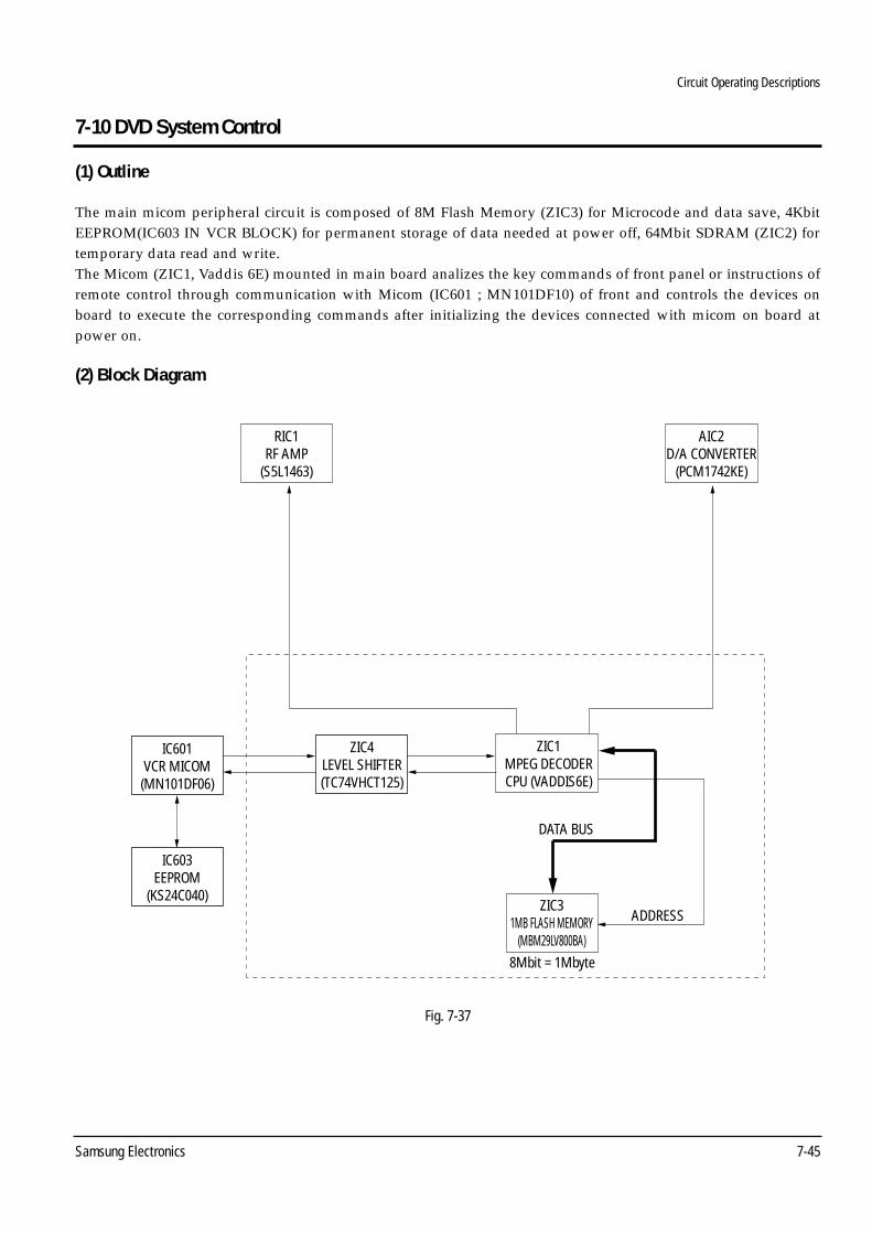
7-10 DVD System Control
(1) Outline
The main micom peripheral circuit is composed of 8M Flash Memory (ZIC3) for Microcode and data save, 4KbitEEPROM(IC603 IN VCR BLOCK) for permanent storage of data needed at power off, 64Mbit SDRAM (ZIC2) fortemporary data read and write.The Micom (ZIC1, Vaddis 6E) mounted in main board analizes the key commands of front panel or instructions ofremote control through communication with Micom (IC601 ; MN101DF10) of front and controls the devices onboard to execute the corresponding commands after initializing the devices connected with micom on board atpower on.
(2) Block Diagram
RIC1RF AMP
(S5L1463)
AIC2D/A CONVERTER
(PCM1742KE)
ZIC1MPEG DECODERCPU (VADDIS6E)
ZIC31MB FLASH MEMORY
(MBM29LV800BA)
DATA BUS
IC601VCR MICOM(MN101DF06)
IC603EEPROM
(KS24C040)
ZIC4LEVEL SHIFTER(TC74VHCT125)
ADDRESS
8Mbit = 1Mbyte
Fig. 7-37

Circuit Operating Descriptions
7-46 Samsung Electronics
7-11 RF
7-11-1 RIC1 (SP3723)
SP3723 is combined with Zoran Vaddis 6 as bipolar IC developed for DVD SERVO system. Main features include DVD waveform equalizing, CD waveform equalizing, focus error signal generation, 3-beamtracking error signal generation, DPD 1-beam tracking error, defect, MIRR output, Laser Power Control, etc.
7-11-1 (a) Basic Potentiometer
SP3723 Uses 4.5V to 5.5V and reference voltage is 1.65V.
7-11-1(b) RF signal
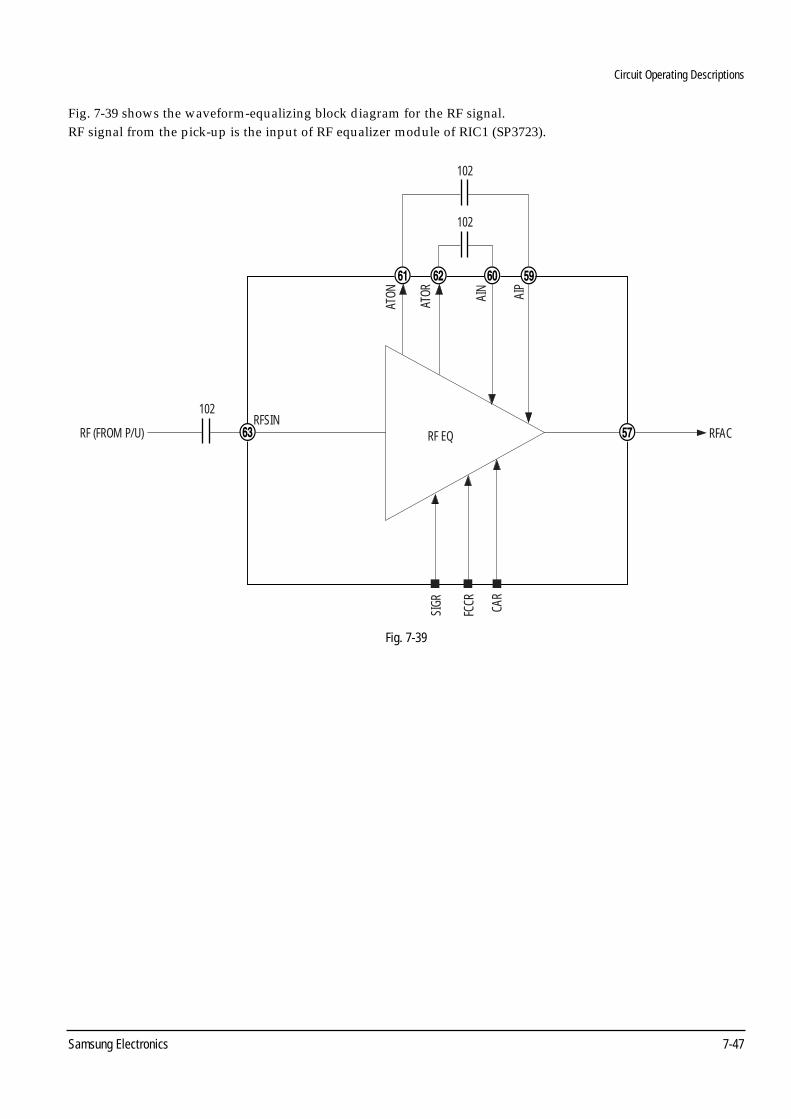
Fig. 7-38 shows the flow of signal generated by the pick-up.RF signal detected from pick-up is converted in to RF signal via RF interface and attennuators.A, B, C, D signals detected from pick-up are converted in to FE, TE, PI, CE, DEFECT signals.
Fig. 7-38
Circuit Operating Descriptions
Samsung Electronics 7-47
RF (FROM P/U) RFACRFSIN
102
102
102
RF EQSI
GR
ATON
ATOR AIN AIP
FCCR CA
R
K
J j Hh
G
Fig. 7-39
Fig. 7-39 shows the waveform-equalizing block diagram for the RF signal.RF signal from the pick-up is the input of RF equalizer module of RIC1 (SP3723).
Circuit Operating Descriptions
7-48 Samsung Electronics
7-12 Servo
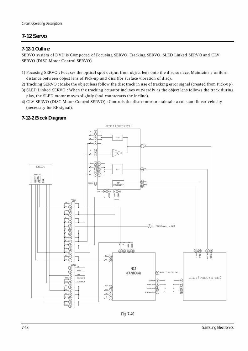
7-12-1 OutlineSERVO system of DVD is Compoced of Focusing SERVO, Tracking SERVO, SLED Linked SERVO and CLV SERVO (DISC Motor Control SERVO).
1) Focusing SERVO : Focuses the optical spot output from object lens onto the disc surface. Maintains a uniform distance between object lens of Pick-up and disc (for surface vibration of disc).
2) Tracking SERVO : Make the object lens follow the disc track in use of tracking error signal (created from Pick-up).3) SLED Linked SERVO : When the tracking actuator inclines outwardly as the object lens follows the track during
play, the SLED motor moves slightly (and counteracts the incline).4) CLV SERVO (DISC Motor Control SERVO) : Controls the disc motor to maintain a constant linear velocity
(necessary for RF signal).
7-12-2 Block Diagram
Fig. 7-40
FIC1(FAN8004)
36
38
1
256
7
4
31011
89
37
35 32 33
8
15
348
11
TM+
LED
POWER
GND
ZIC1(Vaddis 6E)
ZIC1(Vaddis 6E)
TM+ TM1
TM1
OPEN
CLOSE
SP+SP+
SP-SP-
Circuit Operating Descriptions
Samsung Electronics 7-49
7-12-3 Operation
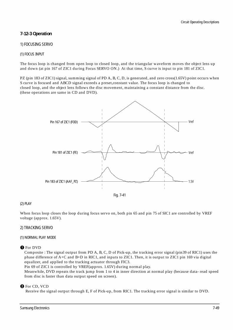
1) FOCUSING SERVO
(1) FOCUS INPUT
The focus loop is changed from open loop to closed loop, and the triangular waveform moves the object lens up and down (at pin 167 of ZIC1 during Focus SERVO ON.) At that time, S curve is input to pin 181 of ZIC1.
PZ (pin 183 of ZIC1) signal, summing signal of PD A, B, C, D, is generated, and zero cross(1.65V) point occurs whenS curve is focused and ABCD signal exceeds a preset,constant value. The focus loop is changed toclosed loop, and the object lens follows the disc movement, maintaining a constant distance from the disc. (these operations are same in CD and DVD).
Fig. 7-41
Vref
Vref
1.5V
Pin 167 of ZIC1 (FOD)
Pin 181 of ZIC1 (FE)
Pin 183 of ZIC1 (AAF_PZ)
(2) PLAY
When focus loop closes the loop during focus servo on, both pin 65 and pin 75 of SIC1 are controlled by VREF voltage (approx. 1.65V).
2) TRACKING SERVO
(1) NORMAL PLAY MODE
ΠFor DVDComposite : The signal output from PD A, B, C, D of Pick-up, the tracking error signal (pin39 of RIC1) uses thephase difference of A+C and B+D in RIC1, and inputs to ZIC1. Then, it is output to ZIC1 pin 169 via digital equalizer, and applied to the tracking actuator through FIC3. Pin 69 of ZIC1 is controlled by VREF(approx. 1.65V) during normal play.Meanwhile, DVD repeats the track jump from 1 to 4 in inner direction at normal play (because data- read speedfrom disc is faster than data output speed on screen).
´ For CD, VCDReceive the signal output through E, F of Pick-up, from RIC1. The tracking error signal is similar to DVD.

Circuit Operating Descriptions
7-50 Samsung Electronics
(2) SEARCH Mode :
Search mode : Fine seek,(Moving the tracking actuator slightly little below 255 track) and coarse search, movingmuch in use of sled motor. The coarse search will be described in sled linked servo and now, the fine seek is explained shortly.If the object lens is located near target, cut off the tracking loop and give the control signal as many as desired count to move the tracking actuator via ZIC1 pin 169 terminal(TRD).
3) SLED LINKED SERVO
• Normal play modeMove SLED motor slightly by means of PWM signal in ZIC1 pin 191, as the tracking actuator moves along with track during play. Control to move the entire Pick-up as the tracking actuator moves.
• Coarse serach modeIn case of long-distance search (such as chapter serach), ZIC1 uses MIRR and Global sense signal.Then, read ID and compute the existing track count after input of next track. If the existing track count is within fine seek range, tracking begins using fine seek.
4) CLV SERVO(DISC MOTOR CONTROL SERVO)
Input RF signal (from Pick-up) to ZIC1 pin 172, 173. Detect SYNC signal from RF in ZIC1, and output PWM signal to ZIC1 pin 189 for constant linear velocity.
Circuit Operating Descriptions
Samsung Electronics 7-51
7-13 DVD Data Processor
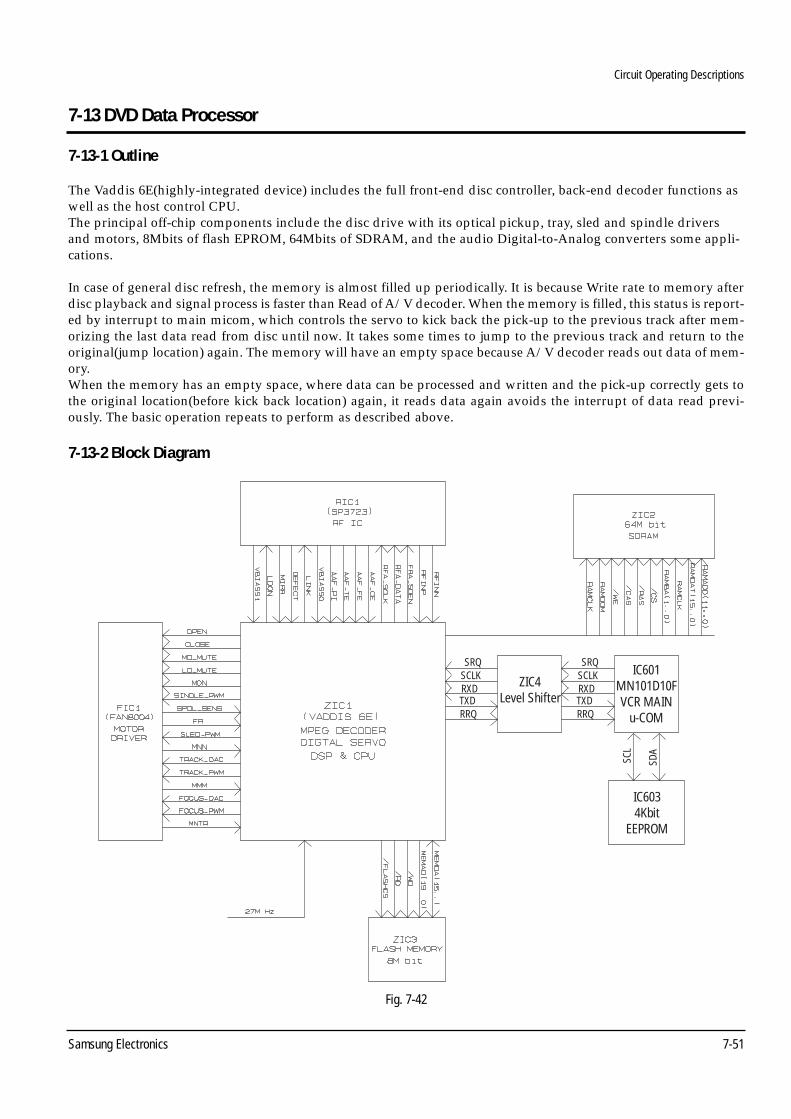
7-13-1 Outline
The Vaddis 6E(highly-integrated device) includes the full front-end disc controller, back-end decoder functions aswell as the host control CPU.The principal off-chip components include the disc drive with its optical pickup, tray, sled and spindle driversand motors, 8Mbits of flash EPROM, 64Mbits of SDRAM, and the audio Digital-to-Analog converters some appli-cations.
In case of general disc refresh, the memory is almost filled up periodically. It is because Write rate to memory afterdisc playback and signal process is faster than Read of A/V decoder. When the memory is filled, this status is report-ed by interrupt to main micom, which controls the servo to kick back the pick-up to the previous track after mem-orizing the last data read from disc until now. It takes some times to jump to the previous track and return to theoriginal(jump location) again. The memory will have an empty space because A/V decoder reads out data of mem-ory.When the memory has an empty space, where data can be processed and written and the pick-up correctly gets tothe original location(before kick back location) again, it reads data again avoids the interrupt of data read previ-ously. The basic operation repeats to perform as described above.
7-13-2 Block Diagram
Fig. 7-42
ZIC4Level Shifter
IC601MN101D10FVCR MAIN
u-COM
IC6034Kbit
EEPROM
SRQSCLKRXDTXDRRQ
SCL
SDA
SRQSCLKRXDTXDRRQ
Circuit Operating Descriptions
7-52 Samsung Electronics
7-14 Video
7-14-1 Outline
ZIC1(A/V decoder with video encoder) diverges from the 27MHz crystal, then generates VSYNC and HSYNC. ZIC1(A/V decoder with video encoder) does RGB encoding, copy guard processing and D/A conversion of 8bitvideo data internally inputted from video decoder block by ZIC1.Video signal converted into analog signal is outputted via amplifier of analog part.
A/V DecoderVaddis 6E WithVideo Encoder
ZIC1
VCR MAINu-COMIC601
Video data
LA73054
6dBAMP
&75ohmDrive
LOWPASSFILTER(6MHz)
CVBS
Y
C
Y
Pb
Pr
CVBS CVBS
Y
C
Y
Pb
Pr
Y/R/V
C/B/U
CVBS/G/Y
Fig. 7-43 Video Output Block Diagram
7-14-2 NTSC/PAL Digital Encoder (VADDIS 6E ; Built in video encode)
ZIC1 inputted from pin 161 with 27MHz generates HSYNC and VSYNC which are based on video signal. ZIC1 is synchronous signals with decoded video signal and control the output timing of 8bit video signal of ITU-R601 format.The separate signal is encoded to NTSC/PAL by control of MIC1. The above signals, which are CVBS (Composite Video Burst Synchronized)/G (GREEN)/Y [PIN158],Y (S_VIDEO)/R (RED)/Pr[PIN161] and C (S_VIDEO)/B (BLUE)/Pb [PIN162], are selectively outputted CVBS+S_VIDEO, RGB/Component by the rear switch. In Course of encoding, 8bit data can extend to 10bit or more. To convert the extended data to quantization noise as possible, ZIC1 adopts 10bit D/A converter. ZIC1 perform video en-coding as well as copy protection.
7-14-3 Amplifier (VIC1: LA73054)
VIC1 is 6dB amplifier. Based on CVBS signal, the final output level must be 2Vpp without 75ohm terminal resitance. Because the level of video encoder output is only 1.1Vpp, the level is adjusted with the special amplifier. When mute of pin 5 is high active, if the pin is floating and connecte to power, the output signal is neverouputted. CVBS, Y, C, R, Pb(B), Pr(R) outputted from video encoder are inputted to VIC1 (Pin 2, 8, 6, 16, 14). The signal to which gain is adjusted by amplifier is outputted from jack via 75ohm Resistance (VR11~VR16).
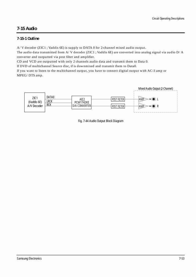
Circuit Operating Descriptions
Samsung Electronics 7-53
7-15 Audio
7-15-1 Outline
A/V decoder (ZIC1 ; Vaddis 6E) is supply to DATA 0 for 2-channel mixed audio output.The audio data transmitted from A/V decoder (ZIC1 ; Vaddis 6E) are converted into analog signal via audio D/Aconverter and outputted via post filter and amplifier.CD and VCD are outputted with only 2 channels audio data and transmit them to Data 0. If DVD of multichannel Source disc, if is downmixed and transmit them to Data0.If you want to listen to the multichannel output, you have to connect digital output with AC-3 amp orMPEG/DTS amp.
AIC2PCM1742KE
D/A CONVERTER
POST FILTER
POST FILTER
AMP
AMP
ZIC1(Vaddis 6E)
A/V Decoder
DATA0LRCKBCK
L
R
Mixed Audio Output (2-Channel)
Fig. 7-44 Audio Output Block Diagram
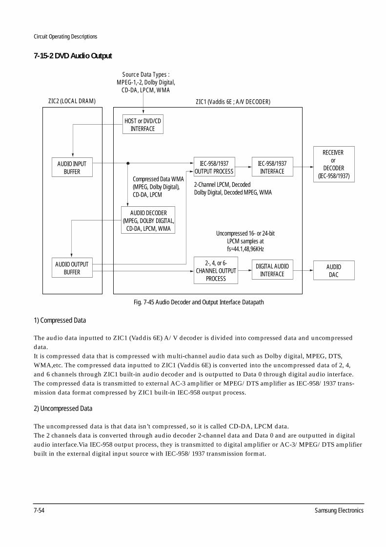
Circuit Operating Descriptions
7-54 Samsung Electronics
7-15-2 DVD Audio Output
1) Compressed Data
The audio data inputted to ZIC1 (Vaddis 6E) A/V decoder is divided into compressed data and uncompresseddata.It is compressed data that is compressed with multi-channel audio data such as Dolby digital, MPEG, DTS,WMA,etc. The compressed data inputted to ZIC1 (Vaddis 6E) is converted into the uncompressed data of 2, 4, and 6 channels through ZIC1 built-in audio decoder and is outputted to Data 0 through digital audio interface. The compressed data is transmitted to external AC-3 amplifier or MPEG/DTS amplifier as IEC-958/1937 trans-mission data format compressed by ZIC1 built-in IEC-958 output process.
2) Uncompressed Data
The uncompressed data is that data isn’t compressed, so it is called CD-DA, LPCM data. The 2 channels data is converted through audio decoder 2-channel data and Data 0 and are outputted in digitalaudio interface.Via IEC-958 output process, they is transmitted to digital amplifier or AC-3/MPEG/DTS amplifierbuilt in the external digital input source with IEC-958/1937 transmission format.
AUDIO INPUTBUFFER
AUDIO OUTPUTBUFFER
RECEIVER or
DECODER(IEC-958/1937)
AUDIODAC
HOST or DVD/CDINTERFACE
IEC-958/1937OUTPUT PROCESS
IEC-958/1937INTERFACE
AUDIO DECODER(MPEG, DOLBY DIGITAL,
CD-DA, LPCM, WMA
DIGITAL AUDIOINTERFACE
2-, 4, or 6-CHANNEL OUTPUT
PROCESS
Uncompressed 16- or 24-bitLPCM samples atfs=44.1,48,96KHz
2-Channel LPCM, DecodedDolby Digital, Decoded MPEG, WMA
Compressed Data WMA(MPEG, Dolby Digital),CD-DA, LPCM
ZIC2 (LOCAL DRAM) ZIC1 (Vaddis 6E ; A/V DECODER)
Source Data Types :MPEG-1,-2, Dolby Digital,
CD-DA, LPCM, WMA
Fig. 7-45 Audio Decoder and Output Interface Datapath