7 ARM Processor MMU Preliminaryhomepages.wmich.edu/~grantner/ece6050/ARM7100vA_3.pdfARM7100 Data...
56
ARM7100 Data Sheet ARM DDI 0035A 7-1 Preliminary ARM Processor MMU This chapter describes the ARM Processor Memory Management Unit. 7.1 Introduction 7-2 7.2 MMU Program Accessible Registers 7-3 7.3 Address Translation 7-4 7.4 Translation Process 7-5 7.5 Translating Section References 7-8 7.6 Translating Small Page References 7-10 7.7 Translating Large Page References 7-11 7.8 MMU Faults and CPU Aborts 7-12 7.9 Fault Address and Fault Status Registers (FAR and FSR) 7-13 7.10 Domain Access Control 7-14 7.11 Fault Checking Sequence 7-15 7.12 Interaction of the MMU, IDC and Write Buffer 7-18 7.13 Effect of Reset 7-19 7
Transcript of 7 ARM Processor MMU Preliminaryhomepages.wmich.edu/~grantner/ece6050/ARM7100vA_3.pdfARM7100 Data...
ARM7100 Data SheetARM DDI 0035A
7-1
111
Pre
limin
ary
ARM Processor MMU
This chapter describes the ARM Processor Memory Management Unit.
7.1 Introduction 7-2
7.2 MMU Program Accessible Registers 7-3
7.3 Address Translation 7-4
7.4 Translation Process 7-5
7.5 Translating Section References 7-8
7.6 Translating Small Page References 7-10
7.7 Translating Large Page References 7-11
7.8 MMU Faults and CPU Aborts 7-12
7.9 Fault Address and Fault Status Registers (FAR and FSR) 7-13
7.10 Domain Access Control 7-14
7.11 Fault Checking Sequence 7-15
7.12 Interaction of the MMU, IDC and Write Buffer 7-18
7.13 Effect of Reset 7-19
7

ARM Processor MMU
ARM7100 Data SheetARM DDI 0035A
7-2
Pre
limin
ary
7.1 IntroductionThe Memory Management MMU performs two primary functions: it translates virtualaddresses into physical addresses, and it controls memory access permissions. TheMMU hardware required to perform these functions consists of a Translation Look-aside Buffer (TLB), access control logic, and translation table walking logic.
The MMU supports memory accesses based on Sections or Pages. Sections arecomprised of 1MB blocks of memory. Two different page sizes are supported: SmallPages consist of 4kB blocks of memory and Large Pages consist of 64kB blocks ofmemory. (Large Pages are supported to allow mapping of a large region of memorywhile using only a single entry in the TLB). Additional access control mechanisms areextended within Small Pages to 1kB Sub-Pages and within Large Pages to 16kB Sub-Pages.
The MMU also supports the concept of domains - areas of memory that can be definedto possess individual access rights. The Domain Access Control Register is used tospecify access rights for up to 16 separate domains.
The TLB caches 64 translated entries. During most memory accesses, the TLBprovides the translation information to the access control logic.
If the TLB contains a translated entry for the virtual address, the access control logicdetermines whether access is permitted. If access is permitted, the MMU outputs theappropriate physical address corresponding to the virtual address. If access is notpermitted, the MMU signals the CPU to abort.
If the TLB misses (it does not contain a translated entry for the virtual address), thetranslation table walk hardware is invoked to retrieve the translation information froma translation table in physical memory. Once retrieved, the translation information isplaced into the TLB, possibly overwriting an existing value. The entry to be overwrittenis chosen by cycling sequentially through the TLB locations.
When the MMU is turned off (as happens on reset), the virtual address is outputdirectly onto the physical address bus.
ARM Processor MMU
ARM7100 Data SheetARM DDI 0035A
7-3
Pre
limin
ary
7.2 MMU Program Accessible RegistersThe ARM Processor provides several 32-bit registers which determine the operationof the MMU. The format for these registers is shown in ➲Figure 7-1: MMU registersummary on page 7-3. A brief description of the registers is provided below. Eachregister will be discussed in more detail within the section that describes its use.
Data is written to and read from the MMU's registers using the ARM CPU's MRC andMCR coprocessor instructions.
The Translation Table Base Register holds the physical address of the base of thetranslation table maintained in main memory. Note that this base must reside on a16kB boundary.
The Domain Access Control Register consists of sixteen 2-bit fields, each of whichdefines the access permissions for one of the sixteen Domains (D15-D0).
Figure 7-1: MMU register summary
Note The registers not shown are reserved and should not be used.
The Fault Status Register indicates the domain and type of access being attemptedwhen an abort occurred. Bits 7:4 specify which of the sixteen domains (D15-D0) wasbeing accessed when a fault occurred. Bits 3:1 indicate the type of access beingattempted. The encoding of these bits is different for internal and external faults (asindicated by bit 0 in the register) and is shown in ➲Table 7-4: Priority encoding of faultstatus on page 7-13. A write to this register flushes the TLB.
The Fault Address Register holds the virtual address of the access which wasattempted when a fault occurred. A write to this register causes the data written to betreated as an address and, if it is found in the TLB, the entry is marked as invalid. (Thisoperation is known as a TLB purge). The Fault Status Register and Fault AddressRegister are only updated for data faults, not for prefetch faults.
Domain Access Control
0 Control 1 D P W AC M
Translation Table Base
0123456789101112131415
0 0 0 0 Domain Status
012345678910111213141516171819202122232425262728293031
Flush TLB
Purge Address
Fault Address
Register
1 write
2 write
3 write
5 read
5 write
6 read
6 write
Fault Status
S B0Control0 0 0 0 R
ARM Processor MMU
ARM7100 Data SheetARM DDI 0035A
7-4
Pre
limin
ary
7.3 Address TranslationThe MMU translates virtual addresses generated by the CPU into physical addressesto access external memory, and also derives and checks the access permission.Translation information, which consists of both the address translation data and theaccess permission data, resides in a translation table located in physical memory. TheMMU provides the logic needed to traverse this translation table, obtain the translatedaddress, and check the access permission.
There are three routes by which the address translation (and hence permission check)takes place. The route taken depends on whether the address in question has beenmarked as a section-mapped access or a page-mapped access; and there are twosizes of page-mapped access (large pages and small pages). However, the translationprocess always starts out in the same way, as described below, with a Level One fetch.A section-mapped access only requires a Level One fetch, but a page-mapped accessalso requires a Level Two fetch.

ARM Processor MMU
ARM7100 Data SheetARM DDI 0035A
7-5
Pre
limin
ary
7.4 Translation Process
7.4.1 Translation table base
The translation process is initiated when the on-chip TLB does not contain an entry forthe requested virtual address. The Translation Table Base (TTB) Register points to thebase of a table in physical memory which contains Section and/or Page descriptors.The 14 low-order bits of the TTB Register are set to zero as illustrated in ➲Figure 7-2:Translation table base register; the table must reside on a 16kB boundary.
Figure 7-2: Translation table base register
7.4.2 Level one fetch
Bits 31:14 of the Translation Table Base register are concatenated with bits 31:20 ofthe virtual address to produce a 30-bit address as illustrated in ➲Figure 7-3: Accessingthe translation table first level descriptors. This address selects a four-byte translationtable entry which is a First Level Descriptor for either a Section or a Page (bit1 of thedescriptor returned specifies whether it is for a Section or Page)
.
Figure 7-3: Accessing the translation table first level descriptors
0131431
Translation Table Base
0192031
031
Table Index Section Index
Virtual Address
Translation Base
1314
Translation Table Base
031
Translation Base
1314
0 0
12
Table Index
1812
First Level Descriptor031

ARM Processor MMU
ARM7100 Data SheetARM DDI 0035A
7-6
Pre
limin
ary
7.4.3 Level one descriptor
The Level One Descriptor returned is either a Page Table Descriptor or a SectionDescriptor, and its format varies accordingly. The following figure illustrates the formatof Level One Descriptors.
Figure 7-4: Level one descriptors
The two least significant bits indicate the descriptor type and validity, and areinterpreted as shown below..
7.4.4 Page table descriptor
Bits 3:2 are always written as 0.
Bit 4 should be written to 1 for backward compatibility.
Bits 8:5 specify one of the sixteen possible domains (held in the Domain AccessControl Register) that contain the primary access controls.
Bits 31:10 form the base for referencing the Page Table Entry. (The page table indexfor the entry is derived from the virtual address as illustrated in ➲Figure 7-7: Smallpage translation on page 7-10).
If a Page Table Descriptor is returned from the Level One fetch, a Level Two fetch isinitiated as described below.
Value Meaning Notes
0 0 Invalid Generates a Section Translation Fault
0 1 Page Indicates that this is a Page Descriptor
1 0 Section Indicates that this is a Section Descriptor
1 1 Reserved Reserved for future use
Table 7-1: Interpreting level one descriptor bits [1:0]
01234589101112192031
0 Fault
Page
Section
Reserved
0
0 1
1 0
1 1
C B
Domain
DomainAP
Page Table Base Address
Section Base Address 1
1
ARM Processor MMU
ARM7100 Data SheetARM DDI 0035A
7-7
Pre
limin
ary
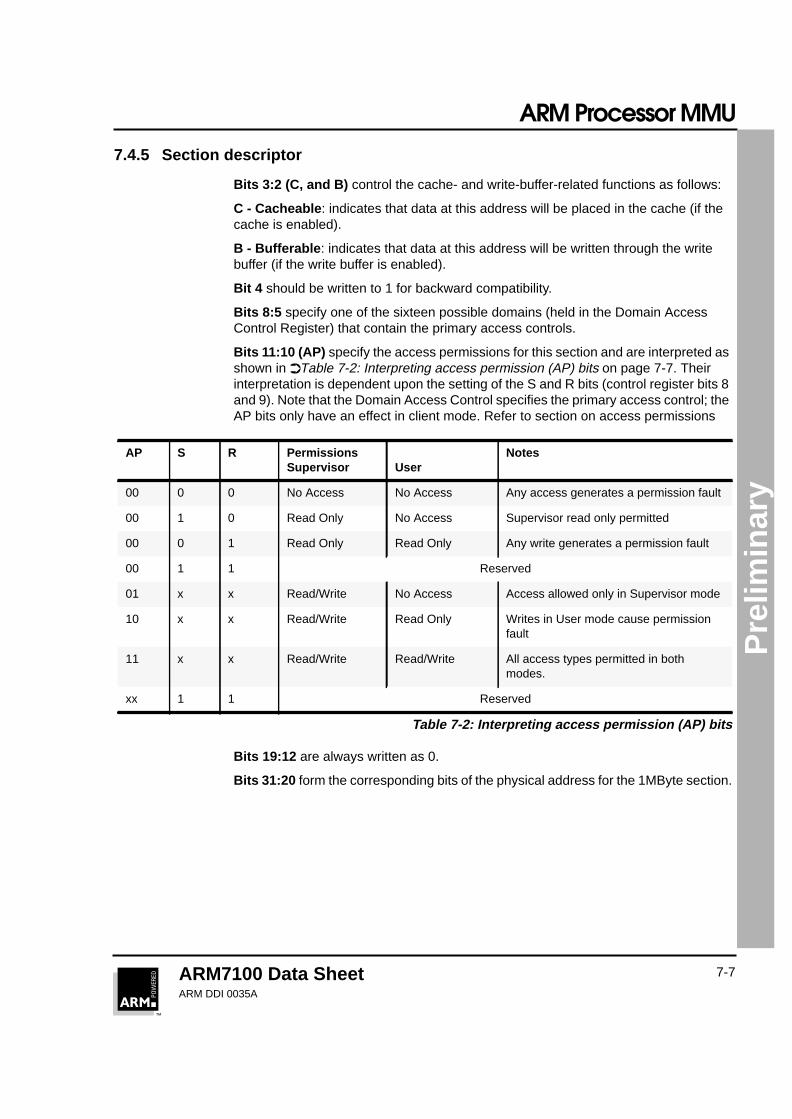
7.4.5 Section descriptor
Bits 3:2 (C, and B) control the cache- and write-buffer-related functions as follows:
C - Cacheable : indicates that data at this address will be placed in the cache (if thecache is enabled).
B - Bufferable : indicates that data at this address will be written through the writebuffer (if the write buffer is enabled).
Bit 4 should be written to 1 for backward compatibility.
Bits 8:5 specify one of the sixteen possible domains (held in the Domain AccessControl Register) that contain the primary access controls.
Bits 11:10 (AP) specify the access permissions for this section and are interpreted asshown in ➲Table 7-2: Interpreting access permission (AP) bits on page 7-7. Theirinterpretation is dependent upon the setting of the S and R bits (control register bits 8and 9). Note that the Domain Access Control specifies the primary access control; theAP bits only have an effect in client mode. Refer to section on access permissions
Bits 19:12 are always written as 0.
Bits 31:20 form the corresponding bits of the physical address for the 1MByte section.
AP S R PermissionsSupervisor User
Notes
00 0 0 No Access No Access Any access generates a permission fault
00 1 0 Read Only No Access Supervisor read only permitted
00 0 1 Read Only Read Only Any write generates a permission fault
00 1 1 Reserved
01 x x Read/Write No Access Access allowed only in Supervisor mode
10 x x Read/Write Read Only Writes in User mode cause permissionfault
11 x x Read/Write Read/Write All access types permitted in bothmodes.
xx 1 1 Reserved
Table 7-2: Interpreting access permission (AP) bits
ARM Processor MMU
ARM7100 Data SheetARM DDI 0035A
7-8
Pre
limin
ary
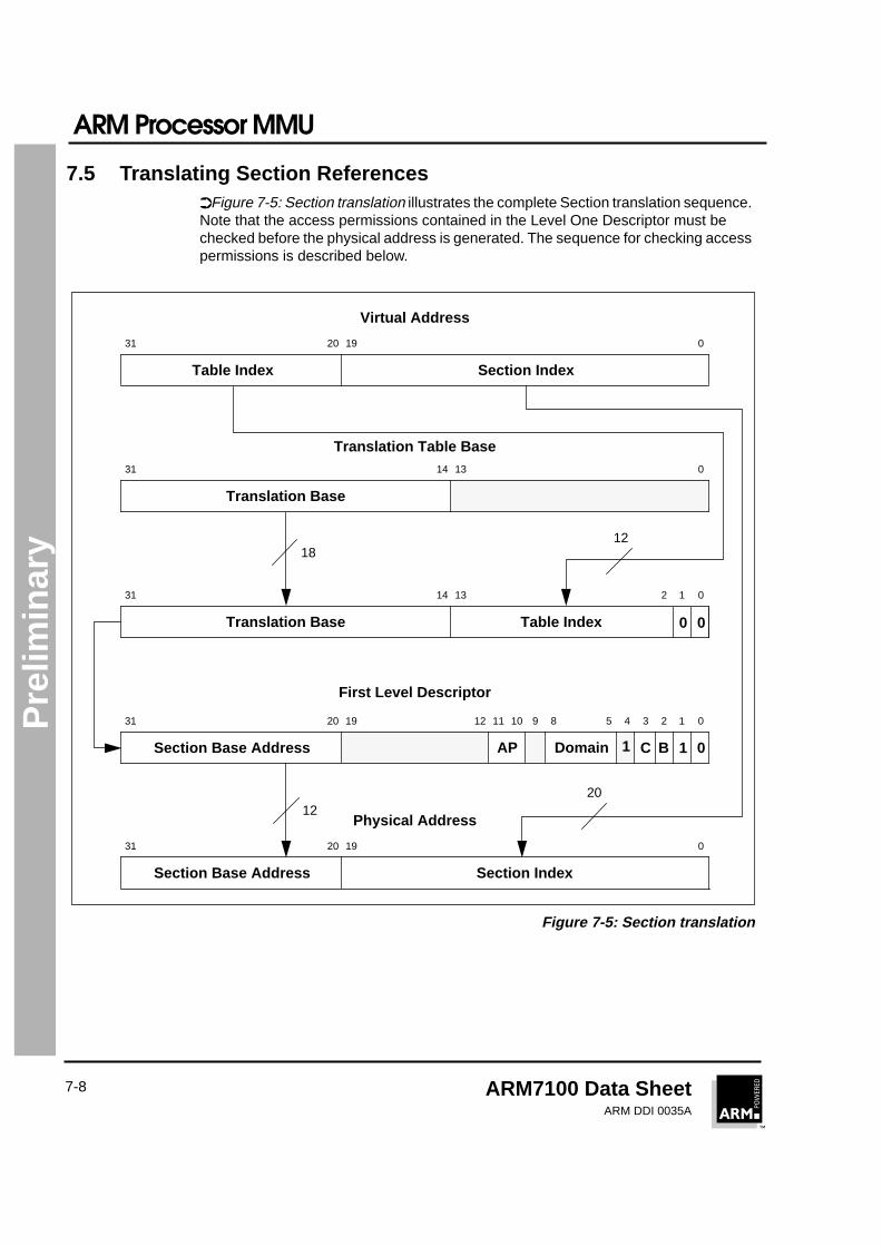
7.5 Translating Section References➲Figure 7-5: Section translation illustrates the complete Section translation sequence.Note that the access permissions contained in the Level One Descriptor must bechecked before the physical address is generated. The sequence for checking accesspermissions is described below.
Figure 7-5: Section translation
0192031
1 0C BDomainAPSection Base Address
031
Table Index Section Index
Virtual Address
Translation Base
01234589101112192031
1314
Translation Table Base
031
Translation Base
1314
0 0
12
Table Index
First Level Descriptor
0192031
Section Base Address Section Index
Physical Address12
20
1812
1
ARM Processor MMU
ARM7100 Data SheetARM DDI 0035A
7-9
Pre
limin
ary
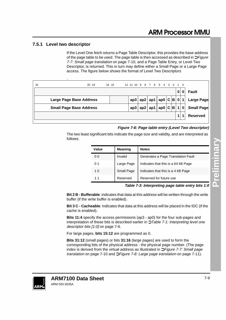
7.5.1 Level two descriptor
If the Level One fetch returns a Page Table Descriptor, this provides the base addressof the page table to be used. The page table is then accessed as described in ➲Figure7-7: Small page translation on page 7-10, and a Page Table Entry, or Level TwoDescriptor, is returned. This in turn may define either a Small Page or a Large Pageaccess. The figure below shows the format of Level Two Descriptors
.
Figure 7-6: Page table entry (Level Two descriptor)
The two least significant bits indicate the page size and validity, and are interpreted asfollows.
Bit 2 B - Bufferable : indicates that data at this address will be written through the writebuffer (if the write buffer is enabled).
Bit 3 C - Cacheable : indicates that data at this address will be placed in the IDC (if thecache is enabled).
Bits 11:4 specify the access permissions (ap3 - ap0) for the four sub-pages andinterpretation of these bits is described earlier in ➲Table 7-1: Interpreting level onedescriptor bits [1:0] on page 7-6.
For large pages, bits 15:12 are programmed as 0.
Bits 31:12 (small pages) or bits 31:16 (large pages) are used to form thecorresponding bits of the physical address - the physical page number. (The pageindex is derived from the virtual address as illustrated in ➲Figure 7-7: Small pagetranslation on page 7-10 and ➲Figure 7-8: Large page translation on page 7-11).
Value Meaning Notes
0 0 Invalid Generates a Page Translation Fault
0 1 Large Page Indicates that this is a 64 kB Page
1 0 Small Page Indicates that this is a 4 kB Page
1 1 Reserved Reserved for future use
Table 7-3: Interpreting page table entry bits 1:0
01234589101112192031
0 Fault
Large Page
Small Page
Reserved
0
0 1
1 0
1 1
C Bap3
Large Page Base Address
Small Page Base Address
671516
ap3
ap2
ap2
ap1
ap1
ap0
ap0 C B
ARM Processor MMU
ARM7100 Data SheetARM DDI 0035A
7-10
Pre
limin
ary
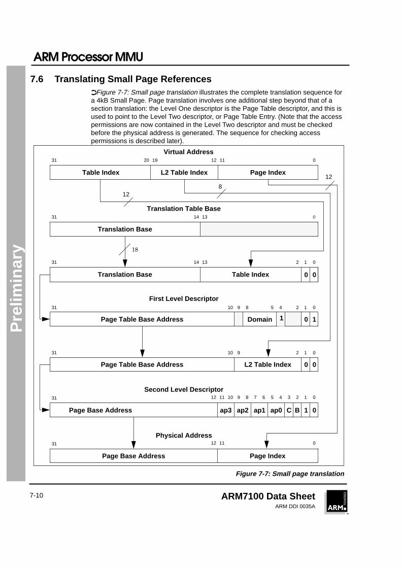
7.6 Translating Small Page References➲Figure 7-7: Small page translation illustrates the complete translation sequence fora 4kB Small Page. Page translation involves one additional step beyond that of asection translation: the Level One descriptor is the Page Table descriptor, and this isused to point to the Level Two descriptor, or Page Table Entry. (Note that the accesspermissions are now contained in the Level Two descriptor and must be checkedbefore the physical address is generated. The sequence for checking accesspermissions is described later).
Figure 7-7: Small page translation
0192031
031
Table Index Page Index
Virtual Address
Translation Base
1314
Translation Table Base
031
Translation Base
1314
0 0
12
Table Index
First Level Descriptor
18
12
0 1DomainPage Table Base Address
01245891031
0 0Page Table Base Address
01291031
L2 Table Index
1112
L2 Table Index
1 0C Bap3Page Base Address
0123458910111231
Second Level Descriptor67
ap2 ap1 ap0
Page Base Address
0111231
Page Index
Physical Address
12
8
1
ARM Processor MMU
ARM7100 Data SheetARM DDI 0035A
7-11
Pre
limin
ary
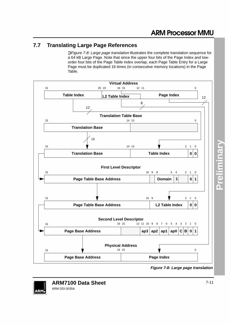
7.7 Translating Large Page References➲Figure 7-8: Large page translation illustrates the complete translation sequence fora 64 kB Large Page. Note that since the upper four bits of the Page Index and low-order four bits of the Page Table index overlap, each Page Table Entry for a LargePage must be duplicated 16 times (in consecutive memory locations) in the PageTable.
Figure 7-8: Large page translation
0192031
031
Table Index Page Index
Virtual Address
Translation Base
1314
Translation Table Base
031
Translation Base
1314
0 0
12
Table Index
First Level Descriptor
18
12
0 1DomainPage Table Base Address
01245891031
0 0Page Table Base Address
01291031
L2 Table Index
1112
L2 Table Index
0 1C Bap3Page Base Address
0123458910111231
Second Level Descriptor67
ap2 ap1 ap0
Page Base Address
031
Page Index
Physical Address
12
8
1516
1516
1516
1

ARM Processor MMU
ARM7100 Data SheetARM DDI 0035A
7-12
Pre
limin
ary
7.8 MMU Faults and CPU AbortsThe MMU generates four types of faults:
Alignment Fault
Translation Fault
Domain Fault
Permission Fault
The access control mechanisms of the MMU detect the conditions that produce thesefaults. If a fault is detected as the result of a memory access, the MMU will abort theaccess and signal the fault condition to the CPU. The MMU is also capable of retainingstatus and address information about the abort. The CPU recognises two types ofabort: data aborts and prefetch aborts, and these are treated differently by the MMU.
If the MMU detects an access violation, it will do so before the external memory accesstakes place, and it will therefore inhibit the access.
If the ARM Processor is operating in fastbus mode an internally aborting access maycause the address on the external address bus to change, even though the externalbus cycle has been cancelled. The address that is placed on the bus will be thetranslation of the address that caused the abort, though in the case of the a TranslationFault the value of this address will be undefined. No memory access will be performedto this address.

ARM Processor MMU
ARM7100 Data SheetARM DDI 0035A
7-13
Pre
limin
ary
7.9 Fault Address and Fault Status Registers (FAR and FSR)Aborts resulting from data accesses (data aborts) are acted upon by the CPUimmediately, and the MMU places an encoded 4-bit value FS[3:0], along with the 4-bitencoded Domain number, in the Fault Status Register (FSR). In addition, the virtualprocessor address which caused the data abort is latched into the Fault AddressRegister (FAR). If an access violation simultaneously generates more than one sourceof abort, they are encoded in the priority given in ➲Table 7-4: Priority encoding of faultstatus on page 7-13.
CPU instructions on the other hand are prefetched, so a prefetch abort simply flagsthe instruction as it enters the instruction pipeline. Only when (and if) the instruction isexecuted does it cause an abort; an abort is not acted upon if the instruction is notused (ie. it is branched around). Because instruction prefetch aborts may or may notbe acted upon, the MMU status information is not preserved for the resulting CPUabort; for a prefetch abort, the MMU does not update the FSR or FAR.
The sections that follow describe the various access permissions and controlssupported by the MMU and detail how these are interpreted to generate faults.
x is undefined, and may read as 0 or 1
Notes
1 Any abort masked by the priority encoding may be regenerated by fixing theprimary abort and restarting the instruction.
2 In fact this register will contain bits[8:5] of the Level 1 entry which areundefined, but would encode the domain in a valid entry.
Source FS[3210] Domain[3:0] FAR
Highest Alignment 00x1 x valid
Bus Error (translation) level1level2
11001110
xvalid
validvalid
Translation SectionPage
01010111
Note 2valid
validvalid
Domain SectionPage
10011011
validvalid
validvalid
Permission SectionPage
11011111
validvalid
validvalid
Bus Error (linefetch) SectionPage
01000110
validvalid
validvalid
Lowest Bus Error (other) SectionPage
10001010
validvalid
validvalid
Table 7-4: Priority encoding of fault status
ARM Processor MMU
ARM7100 Data SheetARM DDI 0035A
7-14
Pre
limin
ary
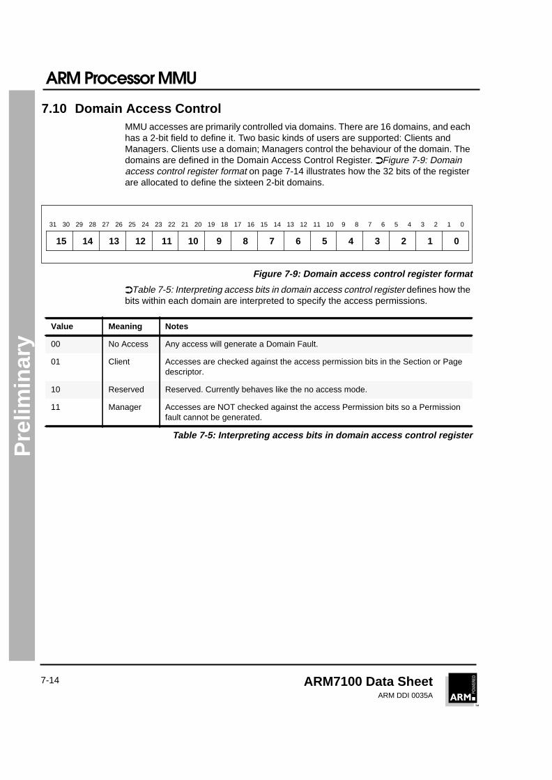
7.10 Domain Access ControlMMU accesses are primarily controlled via domains. There are 16 domains, and eachhas a 2-bit field to define it. Two basic kinds of users are supported: Clients andManagers. Clients use a domain; Managers control the behaviour of the domain. Thedomains are defined in the Domain Access Control Register. ➲Figure 7-9: Domainaccess control register format on page 7-14 illustrates how the 32 bits of the registerare allocated to define the sixteen 2-bit domains.
Figure 7-9: Domain access control register format
➲Table 7-5: Interpreting access bits in domain access control register defines how thebits within each domain are interpreted to specify the access permissions.
Value Meaning Notes
00 No Access Any access will generate a Domain Fault.
01 Client Accesses are checked against the access permission bits in the Section or Pagedescriptor.
10 Reserved Reserved. Currently behaves like the no access mode.
11 Manager Accesses are NOT checked against the access Permission bits so a Permissionfault cannot be generated.
Table 7-5: Interpreting access bits in domain access control register
012345678910111213141516171819202122232425262728293031
0123456789101112131415
ARM Processor MMU
ARM7100 Data SheetARM DDI 0035A
7-15
Pre
limin
ary
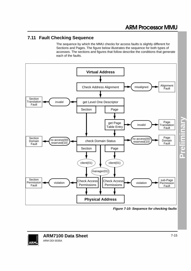
7.11 Fault Checking SequenceThe sequence by which the MMU checks for access faults is slightly different forSections and Pages. The figure below illustrates the sequence for both types ofaccesses. The sections and figures that follow describe the conditions that generateeach of the faults.
Figure 7-10: Sequence for checking faults
violation
no access(00)reserved(10)
Virtual Address
Check Address Alignment
get Level One Descriptor
Section Page
misaligned AlignmentFault
invalidSection
TranslationFault
get PageTable Entry
check Domain Status
invalidPage
TranslationFault
no access(00) PageDomain
Faultreserved(10)
SectionDomain
Fault
Section Page
client(01)client(01)
manager(01)
Check AccessPermissions
Check AccessPermissions
Physical Address
SectionPermission
Faultviolation
sub-PagePermission
Fault
ARM Processor MMU
ARM7100 Data SheetARM DDI 0035A
7-16
Pre
limin
ary
7.11.1 Alignment fault
If Alignment Fault is enabled (bit 1 in Control Register set), the MMU will generate analignment fault on any data word access the address of which is not word-alignedirrespective of whether the MMU is enabled or not; in other words, if either of virtualaddress bits [1:0] are not 0. Alignment fault will not be generated on any instructionfetch, nor on any byte access. Note that if the access generates an alignment fault, theaccess sequence will abort without reference to further permission checks.
7.11.2 Translation fault
There are two types of translation fault: section and page.
1 A Section Translation Fault is generated if the Level One descriptor is markedas invalid. This happens if bits[1:0] of the descriptor are both 0 or both 1.
2 A Page Translation Fault is generated if the Page Table Entry is marked asinvalid. This happens if bits[1:0] of the entry are both 0 or both 1.
7.11.3 Domain fault
There are two types of domain fault: section and page. In both cases the Level Onedescriptor holds the 4-bit Domain field which selects one of the sixteen 2-bit domainsin the Domain Access Control Register. The two bits of the specified domain are thenchecked for access permissions as detailed in ➲Table 7-2: Interpreting accesspermission (AP) bits on page 7-7. In the case of a section, the domain is checked oncethe Level One descriptor is returned, and in the case of a page, the domain is checkedonce the Page Table Entry is returned.
If the specified access is either No Access (00) or Reserved (10) then either a SectionDomain Fault or Page Domain Fault occurs.
7.11.4 Permission fault
There are two types of permission fault: section and sub-page. Permission fault ischecked at the same time as Domain fault. If the 2-bit domain field returns client (01),then the permission access check is invoked as follows:
section:
If the Level One descriptor defines a section-mapped access, then the AP bits of thedescriptor define whether or not the access is allowed according to ➲Table 7-2:Interpreting access permission (AP) bits on page 7-7. Their interpretation is dependentupon the setting of the S bit (Control Register bit 8). If the access is not allowed, thena Section Permission fault is generated.
ARM Processor MMU
ARM7100 Data SheetARM DDI 0035A
7-17
Pre
limin
ary
sub-page:
If the Level One descriptor defines a page-mapped access, then the Level Twodescriptor specifies four access permission fields (ap3..ap0) each corresponding toone quarter of the page. Hence for small pages, ap3 is selected by the top 1kB of thepage, and ap0 is selected by the bottom 1kB of the page; for large pages, ap3 isselected by the top 16kB of the page, and ap0 is selected by the bottom 16kB of thepage. The selected AP bits are then interpreted in exactly the same way as for asection (see ➲Table 7-2: Interpreting access permission (AP) bits on page 7-7), theonly difference being that the fault generated is a sub-page permission fault.
ARM Processor MMU
ARM7100 Data SheetARM DDI 0035A
7-18
Pre
limin
ary
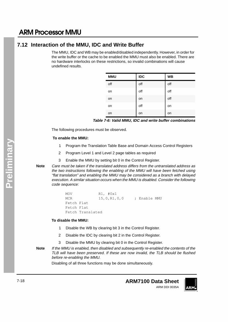
7.12 Interaction of the MMU, IDC and Write BufferThe MMU, IDC and WB may be enabled/disabled independently. However, in order forthe write buffer or the cache to be enabled the MMU must also be enabled. There areno hardware interlocks on these restrictions, so invalid combinations will causeundefined results.
The following procedures must be observed.
To enable the MMU:
1 Program the Translation Table Base and Domain Access Control Registers
2 Program Level 1 and Level 2 page tables as required
3 Enable the MMU by setting bit 0 in the Control Register.
Note Care must be taken if the translated address differs from the untranslated address asthe two instructions following the enabling of the MMU will have been fetched using“flat translation” and enabling the MMU may be considered as a branch with delayedexecution. A similar situation occurs when the MMU is disabled. Consider the followingcode sequence:
MOV R1, #0x1MCR 15,0,R1,0,0 ; Enable MMUFetch FlatFetch FlatFetch Translated
To disable the MMU:
1 Disable the WB by clearing bit 3 in the Control Register.
2 Disable the IDC by clearing bit 2 in the Control Register.
3 Disable the MMU by clearing bit 0 in the Control Register.
Note If the MMU is enabled, then disabled and subsequently re-enabled the contents of theTLB will have been preserved. If these are now invalid, the TLB should be flushedbefore re-enabling the MMU.
Disabling of all three functions may be done simultaneously.
MMU IDC WB
off off off
on off off
on on off
on off on
on on on
Table 7-6: Valid MMU, IDC and write buffer combinations
ARM Processor MMU
ARM7100 Data SheetARM DDI 0035A
7-19
Pre
limin
ary
7.13 Effect of ResetSee ➲4.7 Reset on page 4-16.

ARM Processor MMU
ARM7100 Data SheetARM DDI 0035A
7-20
Pre
limin
ary
ARM7100 Data SheetARM DDI 0035A
8-1
111
Pre
limin
ary
ARM7100 Programmer’s Model
This chapter details the programmable registers for ARM7100.
8.1 Introduction 8-2
8.2 Summary of Registers 8-3
8.3 Register Descriptions 8-5
8
ARM7100 Programmer’s Model
ARM7100 Data SheetARM DDI 0035A
8-2
Pre
limin
ary
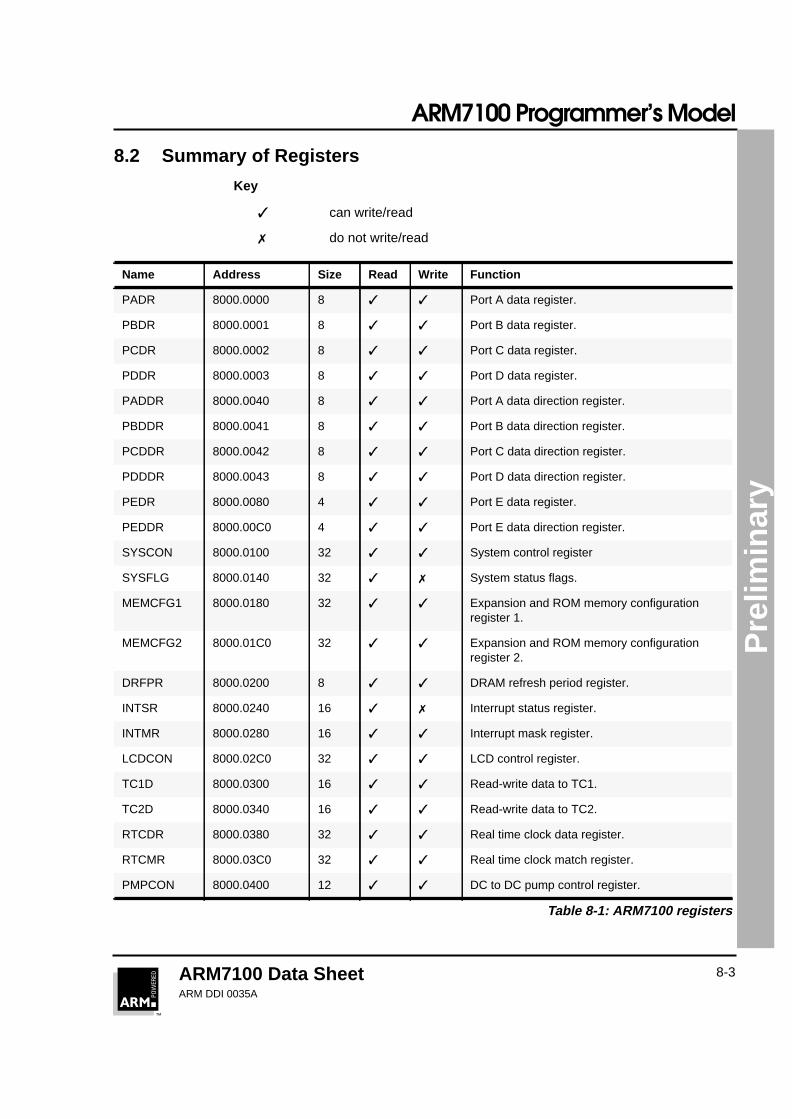
8.1 IntroductionARM7100 contains internal programmable registers in addition to those in the ARMprocessor.
The registers internal to ARM7100 are all programmed by writing to memory locations8000.0000 to 8000.FFFF. Accessing memory in this range will not cause any externalbus activity unless broadcast mode is enabled. Any access to the undefined rangefrom 8000.1000 to C000.0000 will have no effect.
Writes to bits that are not explicitly defined in the internal area are legal and will haveno effect. Reads from bits not explicitly defined in the internal area are legal but willread undefined values.
It is only possible to access internal addresses as 32-bit words and they are alwayson a word boundary, except for the PIO port registers which can be accessed as bytes.Each internal register is valid for 256 bytes, since address bits in the range A[0:5] arenot decoded, for example, the SYSFLG register appears at locations 8000.0140 to8000.017C. The PIO port registers are byte wide but can be accessed as a word.These registers additionally decode A0 and A1.
ARM7100 Programmer’s Model
ARM7100 Data SheetARM DDI 0035A
8-3
Pre
limin
ary
8.2 Summary of Registers
Key
✓ can write/read
✗ do not write/read
Name Address Size Read Write Function
PADR 8000.0000 8 ✓ ✓ Port A data register.
PBDR 8000.0001 8 ✓ ✓ Port B data register.
PCDR 8000.0002 8 ✓ ✓ Port C data register.
PDDR 8000.0003 8 ✓ ✓ Port D data register.
PADDR 8000.0040 8 ✓ ✓ Port A data direction register.
PBDDR 8000.0041 8 ✓ ✓ Port B data direction register.
PCDDR 8000.0042 8 ✓ ✓ Port C data direction register.
PDDDR 8000.0043 8 ✓ ✓ Port D data direction register.
PEDR 8000.0080 4 ✓ ✓ Port E data register.
PEDDR 8000.00C0 4 ✓ ✓ Port E data direction register.
SYSCON 8000.0100 32 ✓ ✓ System control register
SYSFLG 8000.0140 32 ✓ ✗ System status flags.
MEMCFG1 8000.0180 32 ✓ ✓ Expansion and ROM memory configurationregister 1.
MEMCFG2 8000.01C0 32 ✓ ✓ Expansion and ROM memory configurationregister 2.
DRFPR 8000.0200 8 ✓ ✓ DRAM refresh period register.
INTSR 8000.0240 16 ✓ ✗ Interrupt status register.
INTMR 8000.0280 16 ✓ ✓ Interrupt mask register.
LCDCON 8000.02C0 32 ✓ ✓ LCD control register.
TC1D 8000.0300 16 ✓ ✓ Read-write data to TC1.
TC2D 8000.0340 16 ✓ ✓ Read-write data to TC2.
RTCDR 8000.0380 32 ✓ ✓ Real time clock data register.
RTCMR 8000.03C0 32 ✓ ✓ Real time clock match register.
PMPCON 8000.0400 12 ✓ ✓ DC to DC pump control register.
Table 8-1: ARM7100 registers
ARM7100 Programmer’s Model
ARM7100 Data SheetARM DDI 0035A
8-4
Pre
limin
ary
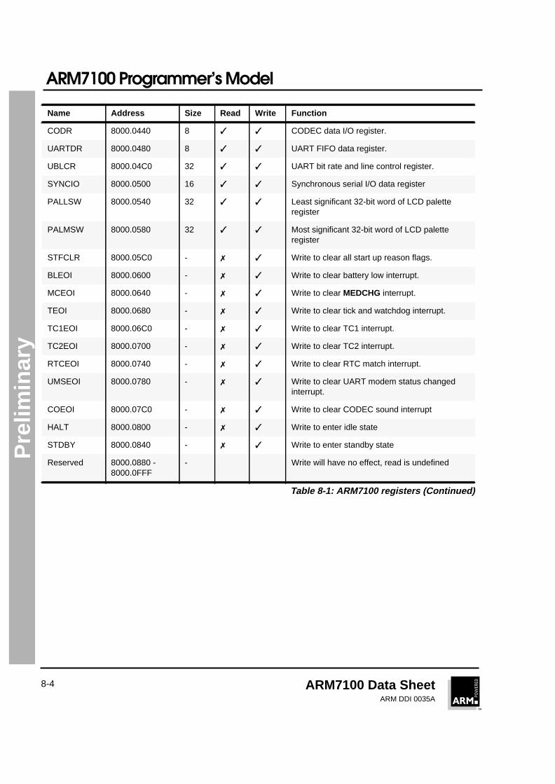
CODR 8000.0440 8 ✓ ✓ CODEC data I/O register.
UARTDR 8000.0480 8 ✓ ✓ UART FIFO data register.
UBLCR 8000.04C0 32 ✓ ✓ UART bit rate and line control register.
SYNCIO 8000.0500 16 ✓ ✓ Synchronous serial I/O data register
PALLSW 8000.0540 32 ✓ ✓ Least significant 32-bit word of LCD paletteregister
PALMSW 8000.0580 32 ✓ ✓ Most significant 32-bit word of LCD paletteregister
STFCLR 8000.05C0 - ✗ ✓ Write to clear all start up reason flags.
BLEOI 8000.0600 - ✗ ✓ Write to clear battery low interrupt.
MCEOI 8000.0640 - ✗ ✓ Write to clear MEDCHG interrupt.
TEOI 8000.0680 - ✗ ✓ Write to clear tick and watchdog interrupt.
TC1EOI 8000.06C0 - ✗ ✓ Write to clear TC1 interrupt.
TC2EOI 8000.0700 - ✗ ✓ Write to clear TC2 interrupt.
RTCEOI 8000.0740 - ✗ ✓ Write to clear RTC match interrupt.
UMSEOI 8000.0780 - ✗ ✓ Write to clear UART modem status changedinterrupt.
COEOI 8000.07C0 - ✗ ✓ Write to clear CODEC sound interrupt
HALT 8000.0800 - ✗ ✓ Write to enter idle state
STDBY 8000.0840 - ✗ ✓ Write to enter standby state
Reserved 8000.0880 -8000.0FFF
- Write will have no effect, read is undefined
Name Address Size Read Write Function
Table 8-1: ARM7100 registers (Continued)
ARM7100 Programmer’s Model
ARM7100 Data SheetARM DDI 0035A
8-5
Pre
limin
ary
8.3 Register DescriptionsAll internal registers in ARM7100 are reset (cleared to zero) by a system reset (nPOR,nRESET or nPWRFL signals becoming active), except for the DRAM refresh periodregister (DRFPR) which is only reset by nPOR becoming active. This ensures that thecontents of DRAM are preserved though a user reset or power fail condition.Additionally, the real time clock registers are only cleared by nPOR.
8.3.1 Port A data register (PADR)
Values written to this 8-bit read-write register are output on port A pins if thecorresponding data direction bits are set HIGH (port output). Values read from thisregister reflect the external state of port A, not necessarily the value written to it. Allbits are cleared by a system reset.
8.3.2 Port B data register (PBDR)
Values written to this 8-bit read-write register are output on port B pins if thecorresponding data direction bits are set HIGH (port output). Values read from thisregister reflect the external state of port B, not necessarily the value written to it. Allbits are cleared by a system reset.
8.3.3 Port C data register (PCDR)
Values written to this 8-bit read-write register are output on port C pins if thecorresponding data direction bits are set LOW (port output). Values read from thisregister reflect the external state of port C, not necessarily the value written to it. Allbits are cleared by a system reset.
8.3.4 Port D data register (PDDR)
Values written to this 8-bit read-write register are output on port D pins if thecorresponding data direction bits are set LOW (port output). Values read from thisregister reflect the external state of port C, not necessarily the value written to it. Allbits are cleared by a system reset.
8.3.5 Port A data direction register (PADDR)
Bits set in this 8-bit read-write register select the corresponding pin in port A to becomean output. Clearing a bit sets the pin to input. All bits are cleared by a system reset.
8.3.6 Port B data direction register (PBDDR)
Bits set in this 8-bit read-write register select the corresponding pin in port B to becomean output. Clearing a bit sets the pin to input. All bits are cleared by a system reset.
ARM7100 Programmer’s Model
ARM7100 Data SheetARM DDI 0035A
8-6
Pre
limin
ary
8.3.7 Port C data direction register (PCDDR)
Bits cleared in this 8-bit read-write register select the corresponding pin in port C tobecome an output. Setting a bit sets the pin to input. All bits are cleared by a systemreset so that port C is output by default.
8.3.8 Port D data direction register (PDDDR)
Bits cleared in this 8-bit read-write register select the corresponding pin in port D tobecome an output, setting a bit sets the pin to input. All bits are cleared by a systemreset so that port D is output by default.
8.3.9 Port E data register (PEDR)
Values written to this 4-bit read-write register will be output on port E pins if thecorresponding data direction bits are set HIGH (port output). Values read from thisregister reflect the external state of port E, not necessarily the value written to it. Allbits are cleared by a system reset.
8.3.10 Port E data direction register (PDDDR)
Bits set in this 4-bit read-write register will select the corresponding pin in port E tobecome an output, clearing bit sets the pin to input. All bits are cleared by a systemreset so that port E is input by default.
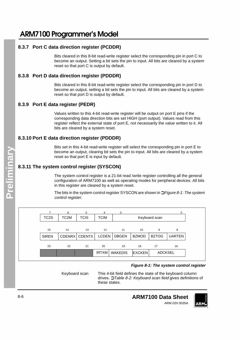
8.3.11 The system control register (SYSCON)
The system control register is a 21-bit read /write register controlling all the generalconfiguration of ARM7100 as well as operating modes for peripheral devices. All bitsin this register are cleared by a system reset.
The bits in the system control register SYSCON are shown in ➲Figure 8-1: The systemcontrol register.
Figure 8-1: The system control register
Keyboard scan This 4-bit field defines the state of the keyboard columndrives. ➲Table 8-2: Keyboard scan field gives definitions ofthese states.
Keyboard scanTCIMTC2S TCISTC2M
ADCKSEL
SIREN CDENTXCDENRX UARTENBZMODDBGENLCDEN
034567
101112131415
17181920212223 16
9 8
BZTOG
EXCKENWAKEDISIRTXM

ARM7100 Programmer’s Model
ARM7100 Data SheetARM DDI 0035A
8-7
Pre
limin
ary
TC1M Timer counter 1 mode. Setting this bit sets TC1 to prescalemode. Clearing it sets free running mode.
TC1S Timer counter 1 clock source. Setting this bit sets the TC1clock source to 512 KHz. Clearing it sets the clock source to2KHz.
TC2M Timer counter 2 mode. Setting this bit sets TC2 to prescalemode. Clearing it sets free running mode.
TC2S Timer counter 2 clock source. Setting this bit sets the TC2clock source to 512 KHz. Clearing it sets the clock source to2KHz.
UARTEN Internal UART enable bit. Setting this bit enables the internalUART.
BZTOG This bit is used to drive the BUZ output directly.
BZMOD This bit sets the BUZ output mode:
0 BUZ is connected directly to the BZTOG bit1 BUZ is connected to the TC1 under flow bit
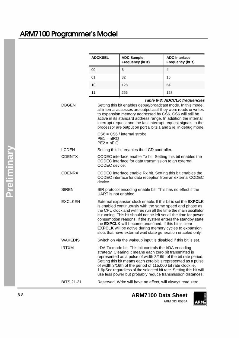
ADCKSEL Microwire / SPI peripheral clock speed select. This 2-bit fieldselects the frequency of the ADC sample clock. This is twicethe frequency of the synchronous serial ADC interface clock.➲Table 8-3: ADCCLK frequencies shows the availablefrequencies.
Keyboard Scan Column
0 All driven HIGH
1 All driven LOW
2 - 7 All Tristate
8 Column 0 only driven HIGH
9 Column 1 only driven HIGH
10 Column 2 only driven HIGH
11 Column 3 only driven HIGH
12 Column 4 only driven HIGH
13 Column 5 only driven HIGH
14 Column 6 only driven HIGH
15 Column 7 only driven HIGH
Table 8-2: Keyboard scan field
ARM7100 Programmer’s Model
ARM7100 Data SheetARM DDI 0035A
8-8
Pre
limin
ary
DBGEN Setting this bit enables debug/broadcast mode. In this mode,all internal accesses are output as if they were reads or writesto expansion memory addressed by CS6. CS6 will still beactive in its standard address range. In addition the internalinterrupt request and the fast interrupt request signals to theprocessor are output on port E bits 1 and 2 ie. in debug mode:
CS6 = CS6 / internal strobePE1 = nIRQPE2 = nFIQ
LCDEN Setting this bit enables the LCD controller.
CDENTX CODEC interface enable Tx bit. Setting this bit enables theCODEC interface for data transmission to an externalCODEC device.
CDENRX CODEC interface enable Rx bit. Setting this bit enables theCODEC interface for data reception from an external CODECdevice.
SIREN SIR protocol encoding enable bit. This has no effect if theUART is not enabled.
EXCLKEN External expansion clock enable. If this bit is set the EXPCLKis enabled continuously with the same speed and phase asthe CPU clock and will free run all the time the main oscillatoris running. This bit should not be left set all the time for powerconsumption reasons. If the system enters the standby statethe EXPCLK will become undefined. If this bit is clearEXPCLK will be active during memory cycles to expansionslots that have external wait state generation enabled only.
WAKEDIS Switch on via the wakeup input is disabled if this bit is set.
IRTXM IrDA Tx mode bit. This bit controls the IrDA encodingstrategy. Clearing it means each zero bit transmitted isrepresented as a pulse of width 3/16th of the bit rate period.Setting this bit means each zero bit is represented as a pulseof width 3/16th of the period of 115,000 bit rate clock ie.1.6µSec regardless of the selected bit rate. Setting this bit willuse less power but probably reduce transmission distances.
BITS 21-31 Reserved. Write will have no effect, will always read zero.
ADCKSEL ADC SampleFrequency (kHz)
ADC InterfaceFrequency (kHz)
00 8 4
01 32 16
10 128 64
11 256 128
Table 8-3: ADCCLK frequencies
ARM7100 Programmer’s Model
ARM7100 Data SheetARM DDI 0035A
8-9
Pre
limin
ary
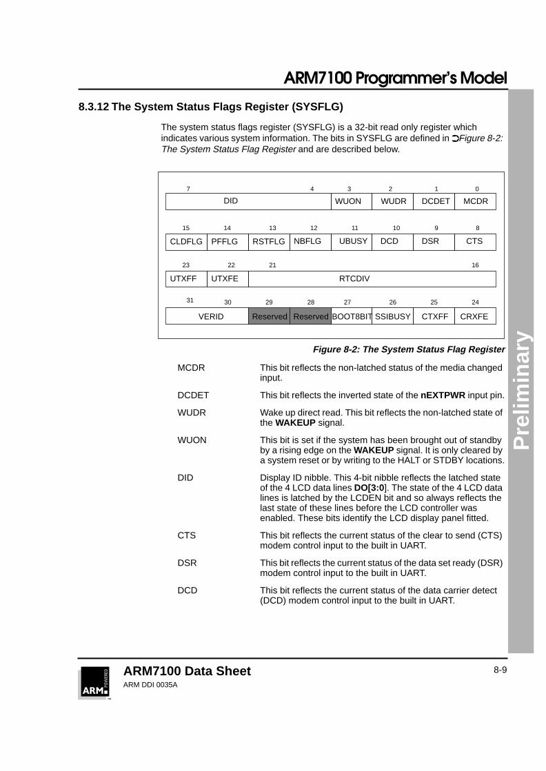
8.3.12 The System Status Flags Register (SYSFLG)
The system status flags register (SYSFLG) is a 32-bit read only register whichindicates various system information. The bits in SYSFLG are defined in ➲Figure 8-2:The System Status Flag Register and are described below.
Figure 8-2: The System Status Flag Register
MCDR This bit reflects the non-latched status of the media changedinput.
DCDET This bit reflects the inverted state of the nEXTPWR input pin.
WUDR Wake up direct read. This bit reflects the non-latched state ofthe WAKEUP signal.
WUON This bit is set if the system has been brought out of standbyby a rising edge on the WAKEUP signal. It is only cleared bya system reset or by writing to the HALT or STDBY locations.
DID Display ID nibble. This 4-bit nibble reflects the latched stateof the 4 LCD data lines DO[3:0 ]. The state of the 4 LCD datalines is latched by the LCDEN bit and so always reflects thelast state of these lines before the LCD controller wasenabled. These bits identify the LCD display panel fitted.
CTS This bit reflects the current status of the clear to send (CTS)modem control input to the built in UART.
DSR This bit reflects the current status of the data set ready (DSR)modem control input to the built in UART.
DCD This bit reflects the current status of the data carrier detect(DCD) modem control input to the built in UART.
DID MCDRWUON DCDETWUDR
CLDFLG RSTFLGPFFLG CTSDSRDCDUBUSYNBFLG
SSIBUSY CRXFE
UTXFF UTXFE RTCDIV
034 127
101112131415
212223
31 30 29 28 27 26 25 24
16
9 8
CTXFFVERID Reserved Reserved BOOT8BIT
ARM7100 Programmer’s Model
ARM7100 Data SheetARM DDI 0035A
8-10
Pre
limin
ary
UBUSY UART transmitter busy. Set while the internal UART is busytransmitting data, it is guaranteed to remain set until thecomplete byte has been sent, including all stop bits.
NBFLG The new battery flag bit is set if a LOW to HIGH transition hasoccurred on the nBATCHG input. It is cleared by writing to theSTFCLR location.
RSTFLG The reset flag is set if the nURESET input has been forcedLOW. It is cleared by writing to the STFCLR location.
PFFLG The Power Fail Flag is set if the system has been reset by thePWRFL input pin. It is cleared by writing to the STFCLRlocation.
CLDFLG The cold start flag is set if ARM7100 has been reset with apower on reset. It is cleared by writing to the STFCLRlocation.
RTCDIV This 6-bit field reflects the number of 64Hz ticks that havepassed since the last increment of the RTC. It is the output ofthe divide by 64 chain that divides the 64Hz tick clock downto 1Hz for the RTC. The MSB is the 32Hz output, the LSB isthe 1Hz output.
URXFE UART receiver FIFO empty. The meaning of this bit dependson the state of the UFIFOEN bit in the UART bit rate and linecontrol register. If the FIFO is disabled, this bit is set when theRx holding register is empty. If the FIFO is enabled theURXFE bit will be set when the Rx FIFO is empty.
UTXFF UART transmit FIFO full. The meaning of this bit depends onthe state of the UFIFOEN bit in the UART bit rate and linecontrol register. If the FIFO is disabled, this bit is set when theTx holding register is full. If the FIFO is enabled the UTXFFbit will be set when the Tx FIFO is full.
CRXFE The CODEC Rx FIFO empty bit is set if the 16 byte CODECRx FIFO is empty.
CTXFF The CODEC Tx FIFO full bit is set if the 16 byte CODEC TxFIFO is full.
SSIBUSY The synchronous serial interface busy bit is set while data isbeing shifted in or out of the synchronous serial interface.When clear, data is valid to read.
Reserved This will always read zero.
VERID Version ID bits. These 2 bits determine the revision id forARM7100. It will read 0 for the first revision.
BOOT8BIT This bit indicates the default (power on reset) bus width of theROM interface. If set, the initial bus width will be 8 bits. Ifclear, it will be 32 bits. See ➲8.3.13 Memory configurationregister 1 (MEMCFG1) on page 8-11 and ➲8.3.14 Memoryconfiguration register 2 (MEMCFG2) on page 8-11 for more

ARM7100 Programmer’s Model
ARM7100 Data SheetARM DDI 0035A
8-11
Pre
limin
ary
details on the ROM interface bus width. The state of this bit isdetermined by the state of Port E bit 0 during power on reset.LOW during power on reset will clear the BOOT8BIT bit andthe system will boot from a 32-bit ROM. HIGH during poweron reset will set the BOOT8BIT bit and the system will bootfrom an 8-bit ROM.
8.3.13 Memory configuration register 1 (MEMCFG1)
The memory configuration register 1 is a 32-bit read-write register which sets theconfiguration of the four expansion and ROM selects nCS[0:3] . Each select isconfigured with a one byte field, starting with expansion select 0.
Figure 8-3: Memory configuration register 1
8.3.14 Memory configuration register 2 (MEMCFG2)
The memory configuration register 2 is a 32-bit read-write register which sets theconfiguration of the four expansion and ROM selects CS[4:7 ]. Each select isconfigured with a one byte field, starting with expansion select 4.
Figure 8-4: Memory configuration register 2
Each of the 8-bit fields in the memory configuration registers are identical and definethe number of wait states, define the bus width, enable the EXPCLK output duringaccesses and enable sequential mode access. This is shown in➲Figure 8-5: Bytefields in the memory configuration register below.
Figure 8-5: Byte fields in the memory configuration register
nCS3 configuration nCS2 configuration nCS0 configurationnCS1 configuration
81516232431 7 0
CS7 configuration CS6 configuration CS4 configurationCS5 configuration
81516232431 7 0
Sequential Access Wait StateSQAEN Bus WidthRandom Access Wait State
23456 1 0
CLKEN
7

ARM7100 Programmer’s Model
ARM7100 Data SheetARM DDI 0035A
8-12
Pre
limin
ary
➲Table 8-4: Values of the bus width field defines the bus width field. The effect of thisfield is dependent on the BOOT8BIT bit which can be read in the SYSFLG register. Allbits in the memory configuration register are cleared by a system reset and the stateof the BOOT8BIT bit is determined by Port E bit 0 pin on ARM7100 during power onreset. In this way, pulling Port E bit 0 either LOW or HIGH during power on reset allowsARM7100 to boot from either 32-bit wide or 8-bit wide ROMs.
When the bus width field is programmed to PCMCIA mode the bus width and busconversion is defined by the state of A[27 ] and A[26] . ➲Table 8-5: PCMCIA mode buswidths on page 8-12 defines the bus width and bus conversion for values of A[27] andA[26] . Word bus conversion converts an ARM 32-bit word access into a series of byteor 16-bit accesses. A special case is 16-bit I/O accesses (A[26] and A[27] HIGH). Inthis case, 32-bit ARM word accesses are not converted into two 16-bit accesses. Thisis to allow individual 16-bit register access. In this mode D[16:31] will be invalid andthe output expansion address bit 1 is selected by the value of A[25] . ARM7100 willalways output 0 on expansion address bit 25, ie. in 16-bit I/O mode processor addressbit 25 becomes PCMIA address bit 1, and PCMIA address bit 25 is 0 limiting the 16-bit I/O address space to 32 Mb.
Note 16-bit I/O accesses are not converted to 32-bit ARM word accesses. This means thatD[16:31] will be invalid during ARM word accesses to this memory area.
Bus Width Field BOOT8BIT Expansion Transfer Mode Port E bit 0 during power on reset
00 0 32-bit wide bus access LOW
01 0 16-bit wide bus access LOW
10 0 8-bit wide bus access LOW
11 0 PCMCIA mode LOW
00 1 8-bit wide bus access HIGH
01 1 PCMCIA mode HIGH
10 1 32-bit wide bus access HIGH
11 1 16-bit wide bus access HIGH
Table 8-4: Values of the bus width field
A26 A27 Bus Width Word Bus Conversion PCMCIA Memory Area
0 0 8 Bits Yes 8-bit attribute memory access
1 0 16 Bits Yes 16-bit common memory access
0 1 8 Bits Yes 8-bit I/O access
1 1 16 Bits No 16-bit I/O access
Table 8-5: PCMCIA mode bus widths
ARM7100 Programmer’s Model
ARM7100 Data SheetARM DDI 0035A
8-13
Pre
limin
ary
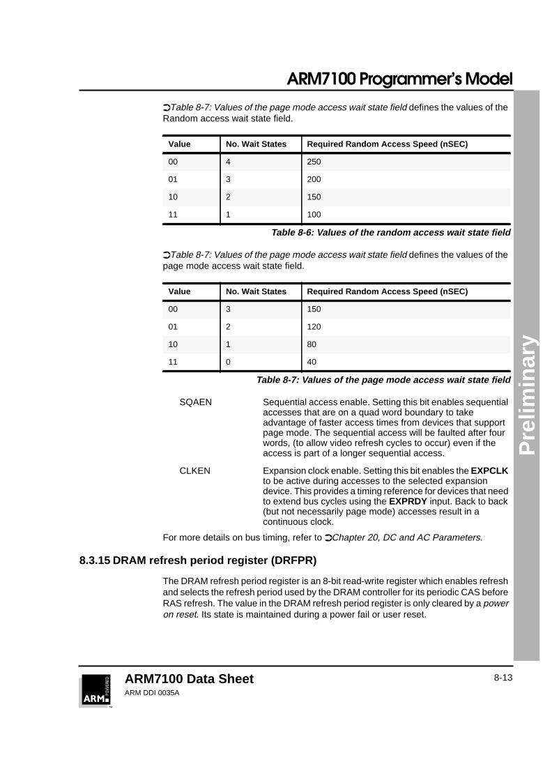
➲Table 8-7: Values of the page mode access wait state field defines the values of theRandom access wait state field.
➲Table 8-7: Values of the page mode access wait state field defines the values of thepage mode access wait state field.
SQAEN Sequential access enable. Setting this bit enables sequentialaccesses that are on a quad word boundary to takeadvantage of faster access times from devices that supportpage mode. The sequential access will be faulted after fourwords, (to allow video refresh cycles to occur) even if theaccess is part of a longer sequential access.
CLKEN Expansion clock enable. Setting this bit enables the EXPCLKto be active during accesses to the selected expansiondevice. This provides a timing reference for devices that needto extend bus cycles using the EXPRDY input. Back to back(but not necessarily page mode) accesses result in acontinuous clock.
For more details on bus timing, refer to ➲Chapter 20, DC and AC Parameters.
8.3.15 DRAM refresh period register (DRFPR)
The DRAM refresh period register is an 8-bit read-write register which enables refreshand selects the refresh period used by the DRAM controller for its periodic CAS beforeRAS refresh. The value in the DRAM refresh period register is only cleared by a poweron reset. Its state is maintained during a power fail or user reset.
Value No. Wait States Required Random Access Speed (nSEC)
00 4 250
01 3 200
10 2 150
11 1 100
Table 8-6: Values of the random access wait state field
Value No. Wait States Required Random Access Speed (nSEC)
00 3 150
01 2 120
10 1 80
11 0 40
Table 8-7: Values of the page mode access wait state field
ARM7100 Programmer’s Model
ARM7100 Data SheetARM DDI 0035A
8-14
Pre
limin
ary
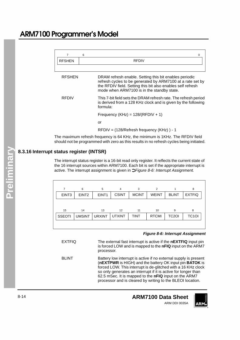
RFSHEN DRAM refresh enable. Setting this bit enables periodicrefresh cycles to be generated by ARM7100 at a rate set bythe RFDIV field. Setting this bit also enables self refreshmode when ARM7100 is in the standby state.
RFDIV This 7-bit field sets the DRAM refresh rate. The refresh periodis derived from a 128 KHz clock and is given by the followingformula:
Frequency (KHz) = 128/(RFDIV + 1)
or
RFDIV = (128/Refresh frequency (KHz) ) - 1
The maximum refresh frequency is 64 KHz, the minimum is 1KHz. The RFDIV fieldshould not be programmed with zero as this results in no refresh cycles being initiated.
8.3.16 Interrupt status register (INTSR)
The interrupt status register is a 16-bit read only register. It reflects the current state ofthe 16 interrupt sources within ARM7100. Each bit is set if the appropriate interrupt isactive. The interrupt assignment is given in ➲Figure 8-6: Interrupt Assignment.
Figure 8-6: Interrupt Assignment
EXTFIQ The external fast interrupt is active if the nEXTFIQ input pinis forced LOW and is mapped to the nFIQ input on the ARM7processor.
BLINT Battery low interrupt is active if no external supply is present(nEXTPWR is HIGH) and the battery OK input pin BATOK isforced LOW. This interrupt is de-glitched with a 16 KHz clockso only generates an interrupt if it is active for longer than62.5 mSec. It is mapped to the nFIQ input on the ARM7processor and is cleared by writing to the BLEOI location.
RFSHEN RFDIV
67 0
EINT3 EINT1EINT2 EXTFIQBLINTWEINTMCINTCSINT
234567 1 8
SSEOTI URXINTUMSINT TC1OITC2OIRTCMITINTUTXINT
101112131415 9 8
ARM7100 Programmer’s Model
ARM7100 Data SheetARM DDI 0035A
8-15
Pre
limin
ary
WEINT Watch dog expired interrupt becomes active on a rising edgeof the periodic 64 Hz tick interrupt clock if the tick interrupt isstill active, ie. if a tick interrupt has not been serviced for acomplete tick period. It is cleared by writing to the TEOIlocation.
MCINT This interrupt is active after a rising edge on the MEDCHGinput pin has been detected, This input is de-glitched with a16 KHz clock so only generates an interrupt if it is active forlonger than 62.5 mSec. It is mapped to the FIQ input on theARM7 processor and is cleared by writing to the MCEOIlocation.
CSINT The CODEC sound interrupt is active if the CODEC interfaceis enabled and the CODEC data FIFO has reached half full orempty (depending on the interface direction). It is cleared bywriting to the COEOI location.
EINT1 The external interrupt input 1 is active if the nEINT1 input isactive (LOW). It is cleared by returning nEINT1 to the passive(HIGH) state.
EINT2 The external interrupt input 2 is active if the NEINT2 input isactive (LOW). It is cleared by returning nEINT2 to the passive(HIGH) state.
EINT3 External interrupt input 3. This input will be active if the EINT3input is active (HIGH). It is cleared by returning EINT3 to thepassive (LOW) state.
TC1OI The TC1 under flow interrupt becomes active on the nextrising edge of the timer counter 1 clock after the timer counterhas under flowed (reached zero). It is cleared by writing to theTC1EOI location.
TC2OI The TC2 under flow interrupt becomes active on the nextrising edge of the timer counter 2 clock after the timer counterhas under flowed (reached zero). It is cleared by writing to theTC2EOI location.
RTCMI The RTC compare match interrupt becomes active on thenext rising edge of the 1Hz real time clock (one second later)after the 32-bit time written to the real time clock matchregister exactly matches the current time in the RTC. It iscleared by writing to the RTCEOI location.
TINT 64 Hz tick interrupt. This interrupt becomes active on everyrising edge of the internal 64Hz clock signal. This 64 Hz clockis derived from the 15 stage ripple counter that divides the32.768 KHz oscillator input down to 1Hz for the real timeclock. This interrupt is cleared by writing to the TEOI location.
ARM7100 Programmer’s Model
ARM7100 Data SheetARM DDI 0035A
8-16
Pre
limin
ary
UTXINT Internal UART transmit FIFO empty interrupt. The function ofthis interrupt source depends on whether the UART FIFO isenabled. If the FIFO is disabled (FIFOEN bit is clear in theUART bit rate and line control register), this interrupt is activewhen there is no data in the UART Tx data holding register. Itis cleared by writing to the UART data register. If the FIFO isenabled, this interrupt is active when the UART Tx FIFO ishalf or more empty, and is cleared by filling the FIFO to atleast half full.
URXINT Internal UART receive FIFO full interrupt. The function of thisinterrupt source depends on whether the UART FIFO isenabled. If the FIFO is disabled this interrupt is active whenthere is valid Rx data in the UART Rx data holding register. Itis cleared by reading this data. If the FIFO is enabled thisinterrupt is active when the UART Rx FIFO is half or more fullor if the FIFO is non empty and no more characters havebeen received for a three character time out period. It iscleared by reading all the data from the Rx FIFO.
UMSINT Internal UART modem status changed interrupt. Thisinterrupt will be active if either of the two modem status lines(CTS or DSR) change state. It is cleared by writing to theUMSEOI location.
SSEOTI Synchronous serial interface end of transfer interrupt. Thisinterrupt is active after a complete data transfer to and fromthe external ADC has completed. It is cleared by reading theADC data from the SYNCIO register.
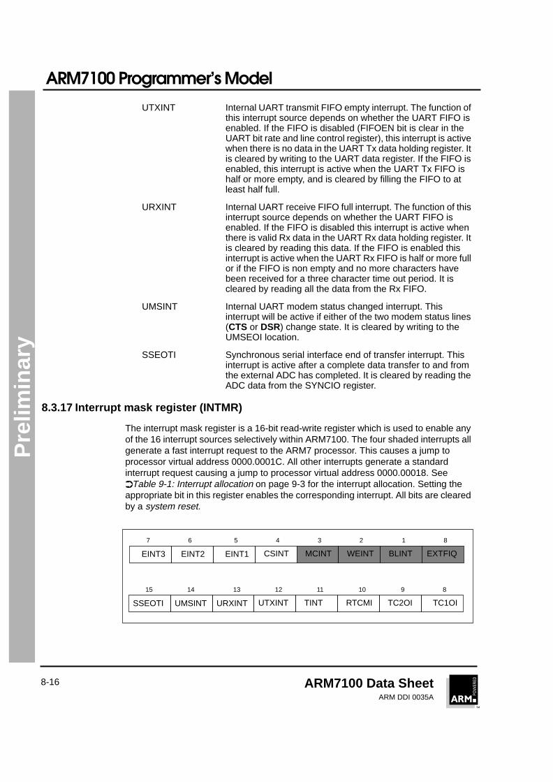
8.3.17 Interrupt mask register (INTMR)
The interrupt mask register is a 16-bit read-write register which is used to enable anyof the 16 interrupt sources selectively within ARM7100. The four shaded interrupts allgenerate a fast interrupt request to the ARM7 processor. This causes a jump toprocessor virtual address 0000.0001C. All other interrupts generate a standardinterrupt request causing a jump to processor virtual address 0000.00018. See➲Table 9-1: Interrupt allocation on page 9-3 for the interrupt allocation. Setting theappropriate bit in this register enables the corresponding interrupt. All bits are clearedby a system reset.
EINT3 EINT1EINT2 EXTFIQBLINTWEINTMCINTCSINT
234567 1 8
SSEOTI URXINTUMSINT TC1OITC2OIRTCMITINTUTXINT
101112131415 9 8

ARM7100 Programmer’s Model
ARM7100 Data SheetARM DDI 0035A
8-17
Pre
limin
ary
8.3.18 The LCD control register (LCDCON)
The LCD control register is a 32-bit read-write register which controls the size of theLCD screen and the mode in which the LCD controller operates. Refer to the systemdescription of the LCD controller for more information on video buffer mapping.
Video buffer size The video buffer size field is a 13-bit field that sets the totalnumber of bytes (*128 quad words) in the video displaybuffer. This is calculated from the following formula:
Video buffer size = (Total bytes in video buffer/128) - 1
For example, for a 640 x 240 LCD and 4 bits per pixel the sizeof the video buffer = 640 x 240 x 4 = 614400 bits.video buffer size field = (614400/128)-1
= 4799 or 0x12BF Hex
Line length The line length field is a 6-bit field that sets the number ofpixels in one complete line. This field is calculated from theformula:
Line length = ( No. pixels in line/16 ) - 1
For example:640 x 240 LCD line length = (640/16)-1
= 39 or 0x27 Hex
Pixel prescale The pixel prescale field is a 6-bit number that sets the pixelrate prescale. The pixel rate is derived from a 36.864 MHzclock and is calculated from the following formula:
Pixel rate (MHz) = 36.864/ (Pixel prescale + 1)
The pixel rate should be chosen to give a complete screenrefresh frequency of approximately 70 Hz to avoid flicker.Frequencies above 70 Hz should be avoided as thisconsumes additional power. The pixel prescale value can beexpressed in terms of the LCD size by the following formula:
Pixel prescale = (526628/Total pixels in display)-1
The value should be rounded down to the nearest wholenumber, and zero is illegal and results in no pixel clock. Forexample:
640 x 240 LCD pixel prescale = 526628/(640x240)-1= 2.428(2)
Actual pixel rate = 36.864E6/2+1=12.288MHz
Actual refresh frequency = 12.288E6/(640x240)= 80Hz
GSENGSMD Video buffer sizeLine lengthPixel prescaleAC prescale
1319293031 12 0182425
ARM7100 Programmer’s Model
ARM7100 Data SheetARM DDI 0035A
8-18
Pre
limin
ary
As the CL2 low pulse time is doubled after every CL1 highpulse, this refresh frequency is only an approximation, theaccurate formula is:
12.288E6/((640x240)+120) =79.937Hz.
AC prescale The AC prescale field is a 5-bit number that sets LCD AC biasfrequency. This frequency is the required AC bias frequencyfor a given manufacturer’s LCD plate. It is derived from thefrequency of the line clock (CL1).
The M signal toggles after n + 1 counts of the line clock (CL1)where n is the number programmed into the AC prescalefield. This number must be chosen to match themanufacturers recommendation. This is normally 13 but mustnot be exactly divisible by the number of lines in the display.
GSEN Grey scale enable bit. Setting this bit enables grey scaleoutput to the LCD. When it is cleared, each bit in the videomap directly corresponds to a pixel in the display.
GSMD Grey scale mode bit. Clearing this bit sets the controller to 2bits per pixel (4 grey scales). Setting it sets it to 4 bits per pixel(15 grey scales).
8.3.19 Timer counter 1 data register (TC1D)
The timer counter 1 data register is a 16-bit read-write register which sets and readsdata to TC1. Any value written will be decremented on the next rising edge of the clock.
8.3.20 Timer counter 2 data register (TC2D)
The timer counter 2 data register is a 16-bit read-write register which sets and readsdata to TC2. Any value written will be decremented on the next rising edge of the clock.
8.3.21 Real time clock data register (RTCDR)
The real time clock data register is a 32-bit read-write register which sets and readsthe binary time in the RTC. Any value written will be incremented on the next risingedge of the 1 Hz clock.
All bits in the real time clock data register are only cleared by an active nPOR.
8.3.22 Real time clock match register (RTCMR)
The real time clock match register is a 32-bit read-write register which sets and readsthe binary match time to RTC. Any value written will be compared to the current binarytime in the RTC, if they match it will assert the RTCMI interrupt source.
8.3.23 Pump control register (PMPCON)
The DC to DC converter pump control register is a 12-bit read-write only register whichsets and controls the variable mark space ratio drives for two DC to DC converters. Allbits in this register are cleared by a system reset.

ARM7100 Programmer’s Model
ARM7100 Data SheetARM DDI 0035A
8-19
Pre
limin
ary
Vh from battery This 4-bit field controls the on time for the DC to DC pump fora Vh rail while the nEXTPWR input is HIGH. Setting thesebits to 0 disables this pump. Setting them to 1 allows thepump to be driven in a 1:16 duty ratio, 2 in a 2:16 duty ratioetc. up to a 15:16 duty ratio. An 8:16 duty ratio results in asquare wave of 96 KHz.
Vh from mains This 4-bit field controls the on time for the DC to DC pump fora Vh rail while the nEXTPWR input is LOW. Setting these bitsto 0 disables this pump. Setting them to 1 allows the pump tobe driven in a 1:16 duty ratio, 2 in a 2:16 duty ratio etc. up toa 15:16 duty ratio. An 8:16 duty ratio results in a square waveof 96 KHz.
VL pump ratio This 4-bit field controls the on time for the DC to DC pump forthe VL voltage rail. Setting these bits to 0 disables this pump.Setting them to 1 allows the pump to be driven in a 1:16 dutyratio, 2 in a 2:16 duty ratio etc. up to a 15:16 duty ratio. An8:16 duty ratio results in a square wave of 96 KHz. The stateof the output drive pin (drive 1) is latched during power onreset, this latched value is used to determine the polarity ofthe bias voltage. The sense of the DC to DC converter controllines is summarised in ➲Table 8-8: Sense of DC to DCConverter Control Lines.
8.3.24 The CODEC interface data register (CODR)
The CODR register is an 8-bit read-write register. Data written to or read from thisregister is pushed or popped onto a 16 byte FIFO buffer. Data from this buffer is thenserialised and sent to or received from the CODEC sound device. The CODECinterrupt CSINT is generated repetitively at 1/8th of the byte transfer rate and the stateof the FIFOs can be read in the system flags register. The net data transfer rate to orfrom the CODEC device is 8 Kb per second giving an interrupt rate of 1 KHz.
Initial State of Drive n during POR Sense of Drive n Polarity of Bias Voltage
LOW Active HIGH +ve
HIGH Active LOW -ve
Table 8-8: Sense of DC to DC Converter Control Lines
Vh from battery ratioVh from mains ratioVL pump ratio
3711 048

ARM7100 Programmer’s Model
ARM7100 Data SheetARM DDI 0035A
8-20
Pre
limin
ary
8.3.25 UART data register (UARTDR)
The UARTDR register is an 11-bit read and an 8-bit write register for all data transfersto or from the internal UART. Data written to this register is pushed onto the 16-bytedata Tx holding FIFO if the FIFO is enabled, or stored in a one byte holding register.This write initiates transmission from the UART. The UART data read register is madeup of the 8-bit data byte received from the UART together with three bits of errorstatus. Data read from this register is popped from the 16 byte data Rx FIFO if theFIFO is enabled, or read from a one byte buffer register containing the last bytereceived and error status if not enabled. Data received by the UART is automaticallypushed onto the Rx FIFO if it is enabled.
The Rx FIFO is 10 bits wide by 16 deep.
FRMERR UART framing error. This bit is set if the UART detected anoverrun or framing error while receiving the Rx data byte.
PARERR UART parity error. This bit is set if the UART detected a parityerror while receiving the Rx data byte.
OVERR UART overrun error. This bit is set if more data is received bythe UART and the FIFO is full. The overrun error bit is notassociated with any single character and so is not stored inthe FIFO. If this bit is set, the entire contents of the FIFO isinvalid and should be cleared. This error bit is cleared byreading the UARTDR register.
8.3.26 UART bit rate and line control register (UBRLCR)
The bit rate divisor and line control register is a 19-bit read-write register. Writing to thisregister sets the bit rate and mode of operation for the internal UART.
Bit rate divisor This 12-bit field sets the bit rate. The bit rate divider is fed bya clock frequency of 3.6864 MHz. It is then further dividedinternally by 16 to give the bit rate. The following formulagives the divisor value for any bit rate:
Divisor = (230400/bit rate)-1
A value of zero in this field is illegal.
PARERROVERR Rx dataFRMERR
7910 08
XSTOPUFIFOEN Bit Rate DivisorBREAKPRTENEVENPRT
12131516 11 0131 14
WRDLEN
1718
ARM7100 Programmer’s Model
ARM7100 Data SheetARM DDI 0035A
8-21
Pre
limin
ary
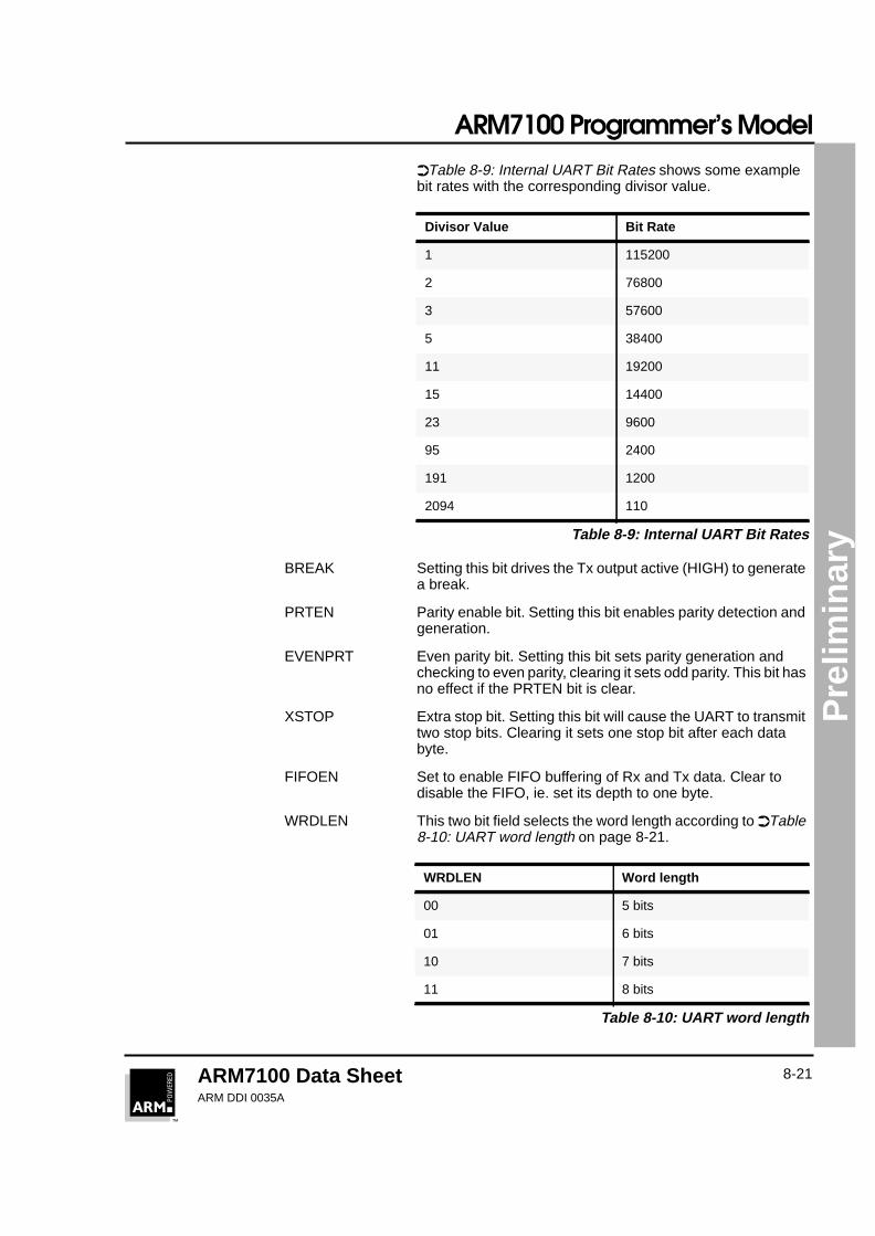
➲Table 8-9: Internal UART Bit Rates shows some examplebit rates with the corresponding divisor value.
BREAK Setting this bit drives the Tx output active (HIGH) to generatea break.
PRTEN Parity enable bit. Setting this bit enables parity detection andgeneration.
EVENPRT Even parity bit. Setting this bit sets parity generation andchecking to even parity, clearing it sets odd parity. This bit hasno effect if the PRTEN bit is clear.
XSTOP Extra stop bit. Setting this bit will cause the UART to transmittwo stop bits. Clearing it sets one stop bit after each databyte.
FIFOEN Set to enable FIFO buffering of Rx and Tx data. Clear todisable the FIFO, ie. set its depth to one byte.
WRDLEN This two bit field selects the word length according to ➲Table8-10: UART word length on page 8-21.
Divisor Value Bit Rate
1 115200
2 76800
3 57600
5 38400
11 19200
15 14400
23 9600
95 2400
191 1200
2094 110
Table 8-9: Internal UART Bit Rates
WRDLEN Word length
00 5 bits
01 6 bits
10 7 bits
11 8 bits
Table 8-10: UART word length
ARM7100 Programmer’s Model
ARM7100 Data SheetARM DDI 0035A
8-22
Pre
limin
ary
8.3.27 Least significant word - LCD palette register (PALLSW)
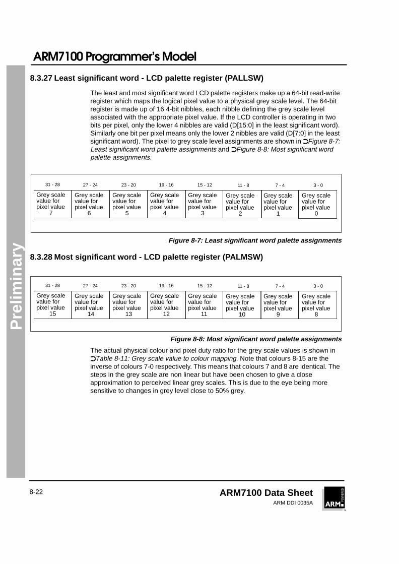
The least and most significant word LCD palette registers make up a 64-bit read-writeregister which maps the logical pixel value to a physical grey scale level. The 64-bitregister is made up of 16 4-bit nibbles, each nibble defining the grey scale levelassociated with the appropriate pixel value. If the LCD controller is operating in twobits per pixel, only the lower 4 nibbles are valid (D[15:0] in the least significant word).Similarly one bit per pixel means only the lower 2 nibbles are valid (D[7:0] in the leastsignificant word). The pixel to grey scale level assignments are shown in ➲Figure 8-7:Least significant word palette assignments and ➲Figure 8-8: Most significant wordpalette assignments.
Figure 8-7: Least significant word palette assignments
8.3.28 Most significant word - LCD palette register (PALMSW)
Figure 8-8: Most significant word palette assignments
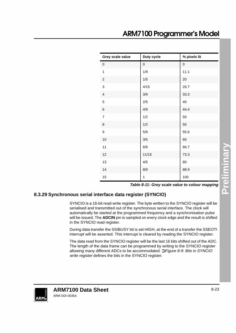
The actual physical colour and pixel duty ratio for the grey scale values is shown in➲Table 8-11: Grey scale value to colour mapping. Note that colours 8-15 are theinverse of colours 7-0 respectively. This means that colours 7 and 8 are identical. Thesteps in the grey scale are non linear but have been chosen to give a closeapproximation to perceived linear grey scales. This is due to the eye being moresensitive to changes in grey level close to 50% grey.
Grey scale
3 - 0
value forpixel value
0
Grey scale
7 - 4
value forpixel value
1
Grey scale
11 - 8
value forpixel value
2
Grey scale
15 - 12
value forpixel value
3
Grey scale
19 - 16
value forpixel value
4
Grey scale
23 - 20
value forpixel value
5
Grey scale
27 - 24
value forpixel value
6
Grey scale
31 - 28
value forpixel value
7
Grey scale
3 - 0
value forpixel value
8
Grey scale
7 - 4
value forpixel value
9
Grey scale
11 - 8
value forpixel value
10
Grey scale
15 - 12
value forpixel value
11
Grey scale
19 - 16
value forpixel value
12
Grey scale
23 - 20
value forpixel value
13
Grey scale
27 - 24
value forpixel value
14
Grey scale
31 - 28
value forpixel value
15
ARM7100 Programmer’s Model
ARM7100 Data SheetARM DDI 0035A
8-23
Pre
limin
ary
8.3.29 Synchronous serial interface data register (SYNCIO)
SYNCIO is a 16-bit read-write register. The byte written to the SYNCIO register will beserialised and transmitted out of the synchronous serial interface. The clock willautomatically be started at the programmed frequency and a synchronisation pulsewill be issued. The ADCIN pin is sampled on every clock edge and the result is shiftedin the SYNCIO read register.
During data transfer the SSIBUSY bit is set HIGH, at the end of a transfer the SSEOTIinterrupt will be asserted. This interrupt is cleared by reading the SYNCIO register.
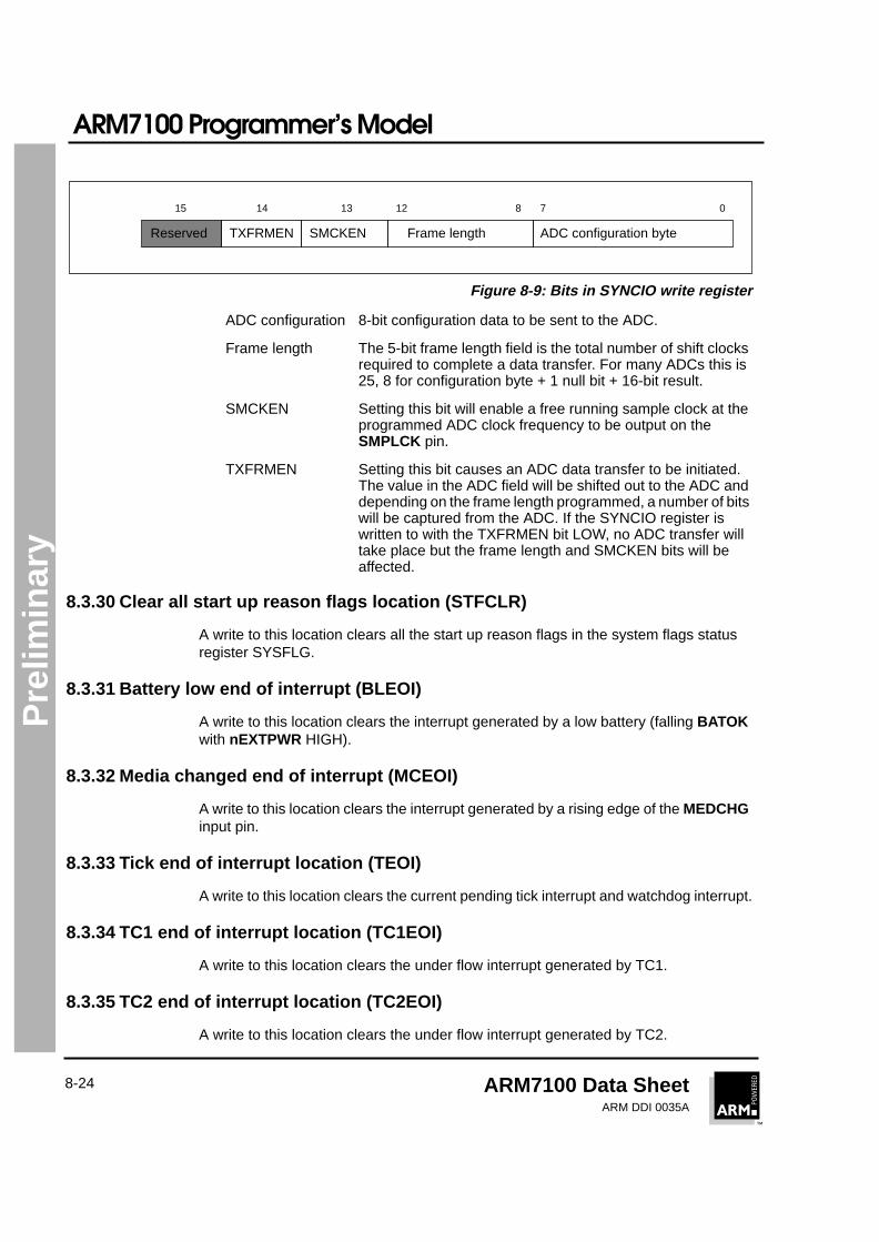
The data read from the SYNCIO register will be the last 16 bits shifted out of the ADC.The length of the data frame can be programmed by writing to the SYNCIO registerallowing many different ADCs to be accommodated. ➲Figure 8-9: Bits in SYNCIOwrite register defines the bits in the SYNCIO register.
Grey scale value Duty cycle % pixels lit
0 0 0
1 1/9 11.1
2 1/5 20
3 4/15 26.7
4 3/9 33.3
5 2/5 40
6 4/9 44.4
7 1/2 50
8 1/2 50
9 5/9 55.6
10 3/5 60
11 6/9 66.7
12 11/15 73.3
13 4/5 80
14 8/9 88.9
15 1 100
Table 8-11: Grey scale value to colour mapping
ARM7100 Programmer’s Model
ARM7100 Data SheetARM DDI 0035A
8-24
Pre
limin
ary
Figure 8-9: Bits in SYNCIO write register
ADC configuration 8-bit configuration data to be sent to the ADC.
Frame length The 5-bit frame length field is the total number of shift clocksrequired to complete a data transfer. For many ADCs this is25, 8 for configuration byte + 1 null bit + 16-bit result.
SMCKEN Setting this bit will enable a free running sample clock at theprogrammed ADC clock frequency to be output on theSMPLCK pin.
TXFRMEN Setting this bit causes an ADC data transfer to be initiated.The value in the ADC field will be shifted out to the ADC anddepending on the frame length programmed, a number of bitswill be captured from the ADC. If the SYNCIO register iswritten to with the TXFRMEN bit LOW, no ADC transfer willtake place but the frame length and SMCKEN bits will beaffected.
8.3.30 Clear all start up reason flags location (STFCLR)
A write to this location clears all the start up reason flags in the system flags statusregister SYSFLG.
8.3.31 Battery low end of interrupt (BLEOI)
A write to this location clears the interrupt generated by a low battery (falling BATOKwith nEXTPWR HIGH).
8.3.32 Media changed end of interrupt (MCEOI)
A write to this location clears the interrupt generated by a rising edge of the MEDCHGinput pin.
8.3.33 Tick end of interrupt location (TEOI)
A write to this location clears the current pending tick interrupt and watchdog interrupt.
8.3.34 TC1 end of interrupt location (TC1EOI)
A write to this location clears the under flow interrupt generated by TC1.
8.3.35 TC2 end of interrupt location (TC2EOI)
A write to this location clears the under flow interrupt generated by TC2.
SMCKENTXFRMEN ADC configuration byteFrame length
781314 012
Reserved
15

ARM7100 Programmer’s Model
ARM7100 Data SheetARM DDI 0035A
8-25
Pre
limin
ary
8.3.36 RTC match end of interrupt (RTCEOI)
A write to this location clears the RTC match interrupt.
8.3.37 UART modem status changed end of interrupt (UMSEOI)
A write to this location clears the modem status changed interrupt.
8.3.38 CODEC end of interrupt location (COEOI)
A write to this location clears the sound interrupt (CSINT).
8.3.39 Enter idle state location (HALT)
A write to this location puts the system into the idle state by halting the clock to theprocessor until an interrupt is generated.
Note If the idle state is entered with no interrupts enabled, there is no mechanism for exitingthe idle state except for a system reset.
8.3.40 Enter standby state location (STDBY)
A write to this location puts the system into the standby state by halting the mainoscillator. It will automatically switch the DRAM's to self refresh if the RFSHEN bit isset in the DRAM refresh period register. All transitions to the standby state aresynchronised with the DRAM cycles.
ARM7100 Programmer’s Model
ARM7100 Data SheetARM DDI 0035A
8-26
Pre
limin
ary
ARM7100 Data SheetARM DDI 0035A
9-1
111
Pre
limin
ary
Interrupt Controller
This chapter describes the interrupt controller.
9.1 Interrupt Controller 9-2
9
Interrupt Controller
ARM7100 Data SheetARM DDI 0035A
9-2
Pre
limin
ary
9.1 Interrupt ControllerThe ARM 710a has two interrupt types:
• interrupt request (IRQ)
• fast interrupt request (FIQ)
The interrupt controller in ARM7100 controls interrupts from 16 different sources.Twelve interrupt sources are mapped to the IRQ input and four sources to the FIQinput. FIQs have a higher priority than IRQs and if two interrupts at the same priorityare active, the priority they are serviced in must be resolved in software.
All interrupts are level sensitive, ie. they must conform to the following sequence:
1 The device asserts the appropriate interrupt request line.
2 If the appropriate bit is set in the interrupt mask register, either FIQ or IRQ isasserted by the interrupt controller.
3 If interrupts are enabled, the processor jumps to the appropriate vector.
4 Interrupt despatch software reads the interrupt control and status register toestablish the source(s) of the interrupt and calls the appropriate interruptservice routine(s).
5 Software in the interrupt service routine clears the interrupt source by anaction specific to the device requesting the interrupt, eg. reading the UART Rxregister.
6 The interrupt service routine may then re-enable interrupts and any otherpending interrupts will be serviced in a similar way, or return to the interruptdispatch code which can check for any more pending interrupts and dispatchthem accordingly.
See ➲Chapter 8, ARM7100 Programmer’s Model for details of interrupt registers.
Interrupt Controller
ARM7100 Data SheetARM DDI 0035A
9-3
Pre
limin
ary
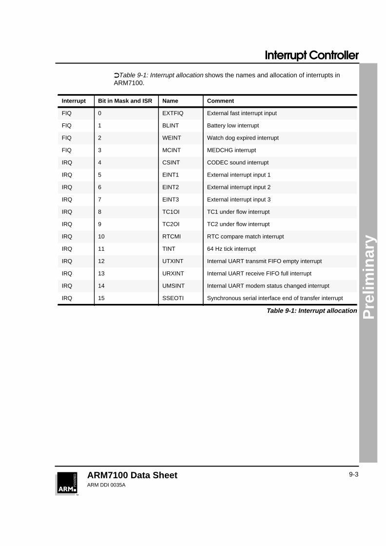
➲Table 9-1: Interrupt allocation shows the names and allocation of interrupts inARM7100.
Interrupt Bit in Mask and ISR Name Comment
FIQ 0 EXTFIQ External fast interrupt input
FIQ 1 BLINT Battery low interrupt
FIQ 2 WEINT Watch dog expired interrupt
FIQ 3 MCINT MEDCHG interrupt
IRQ 4 CSINT CODEC sound interrupt
IRQ 5 EINT1 External interrupt input 1
IRQ 6 EINT2 External interrupt input 2
IRQ 7 EINT3 External interrupt input 3
IRQ 8 TC1OI TC1 under flow interrupt
IRQ 9 TC2OI TC2 under flow interrupt
IRQ 10 RTCMI RTC compare match interrupt
IRQ 11 TINT 64 Hz tick interrupt
IRQ 12 UTXINT Internal UART transmit FIFO empty interrupt
IRQ 13 URXINT Internal UART receive FIFO full interrupt
IRQ 14 UMSINT Internal UART modem status changed interrupt
IRQ 15 SSEOTI Synchronous serial interface end of transfer interrupt
Table 9-1: Interrupt allocation
Interrupt Controller
ARM7100 Data SheetARM DDI 0035A
9-4
Pre
limin
ary

ARM7100 Data SheetARM DDI 0035A
10-1
111
Pre
limin
ary
The Expansion andROM Interface
This chapter describes the ROM Interface.
10.1 The Expansion and ROM Interface 10-2
10

The Expansion and ROM Interface
ARM7100 Data SheetARM DDI 0035A
10-2
Pre
limin
ary
10.1 The Expansion and ROM InterfaceEight separate linear memory or expansion segments are decoded by the ARM7100.Each segment is 256 Mb and can be interfaced to a conventional SRAM-like interface.
Each segment can be programmed individually to:
• be 8, 16 or 32 bits wide
• support page mode access
• execute from 0 to 4 wait states.
In addition, bus cycles can be extended using the EXPRDY input signal.
Page mode access is accomplished by running up to four accesses together. This cansignificantly improve bus bandwidth to devices such as ROMs. Sequential burst modeaccess is always faulted (the bus returned to idle) after four accesses regardless ofbus width to allow DMA and refresh cycles.
See ➲Chapter 8, ARM7100 Programmer’s Model for details of the expansion andROM interface registers.
ARM7100 Data SheetARM DDI 0035A
11-1
111
Pre
limin
ary
DRAM controller
This chapter describes the DRAM controller.
11.1 DRAM Controller 11-2
11

DRAM controller
ARM7100 Data SheetARM DDI 0035A
11-2
Pre
limin
ary
11.1 DRAM ControllerThe DRAM controller in ARM7100 provides connections allowing a direct interface toup to four banks of DRAM. Each bank is 32 bits wide and up to 256 Mb in size. FourRAS lines are provided (one per bank) and four CAS lines (one per byte line). TheDRAM device size is not programmable if devices smaller than the largest sizesupported (1 Gbit) are used. This leads to a segmented memory map with each bankseparated by 256 MBytes. Segments that are smaller than the bank size will repeatwithin the bank.
➲Table 11-1: Physical to DRAM address mapping shows the mapping of physicaladdress to DRAM row and column address. This mapping has been organised tosupport any DRAM device size from 4 Mbit to 1 Gbit with a square row and columnconfiguration, ie. the number of column addresses is equal to the number of rowaddresses. If a non-square DRAM is used, further fragmentation of the memory mapwill occur. However the smallest contiguous segment will always be 1 Mb.
➲Table 11-2: DRAM address mapping shows the address mapping for variousDRAMs with square and non-square row and address inputs, assuming two x16devices are connected to each RAS line. This mapping is repeated every 256 Mb foreach DRAM bank. n is given by n = 0xC + bank number, eg. 0 for bank 0.
Memory Address DRAM Column DRAM Row Pin Name
0 A2 A10 A[27]/DRA[0]
1 A3 A11 A[26]/DRA[1]
2 A4 A12 A[25]/DRA[2]
3 A5 A13 A[24]/DRA[3]
4 A6 A14 A[23]/DRA[4]
5 A7 A15 A[22]/DRA[5]
6 A8 A16 A[21]/DRA[6]
7 A9 A17 A[20]/DRA[7]
8 A19 A18 A[19]/DRA[8]
9 A21 A20 A[18]/DRA[9]
10 A23 A22 A[17]/DRA[10]
11 A25 A24 A[16]/DRA[11]
12 A27 A26 A[15]/DRA[12]
Table 11-1: Physical to DRAM address mapping
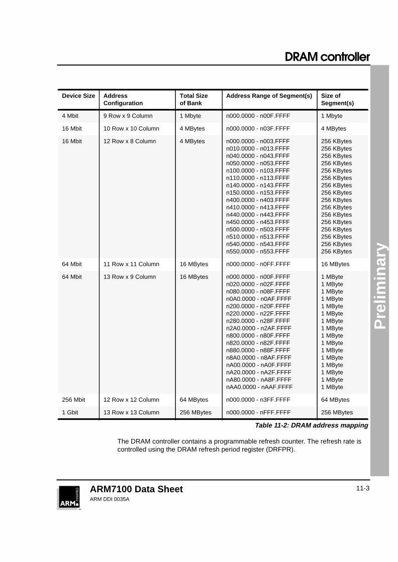
DRAM controller
ARM7100 Data SheetARM DDI 0035A
11-3
Pre
limin
ary
The DRAM controller contains a programmable refresh counter. The refresh rate iscontrolled using the DRAM refresh period register (DRFPR).
Device Size AddressConfiguration
Total Sizeof Bank
Address Range of Segment(s) Size ofSegment(s)
4 Mbit 9 Row x 9 Column 1 Mbyte n000.0000 - n00F.FFFF 1 Mbyte
16 Mbit 10 Row x 10 Column 4 MBytes n000.0000 - n03F.FFFF 4 MBytes
16 Mbit 12 Row x 8 Column 4 MBytes n000.0000 - n003.FFFFn010.0000 - n013.FFFFn040.0000 - n043.FFFFn050.0000 - n053.FFFFn100.0000 - n103.FFFFn110.0000 - n113.FFFFn140.0000 - n143.FFFFn150.0000 - n153.FFFFn400.0000 - n403.FFFFn410.0000 - n413.FFFFn440.0000 - n443.FFFFn450.0000 - n453.FFFFn500.0000 - n503.FFFFn510.0000 - n513.FFFFn540.0000 - n543.FFFFn550.0000 - n553.FFFF
256 KBytes256 KBytes256 KBytes256 KBytes256 KBytes256 KBytes256 KBytes256 KBytes256 KBytes256 KBytes256 KBytes256 KBytes256 KBytes256 KBytes256 KBytes256 KBytes
64 Mbit 11 Row x 11 Column 16 MBytes n000.0000 - n0FF.FFFF 16 MBytes
64 Mbit 13 Row x 9 Column 16 MBytes n000.0000 - n00F.FFFFn020.0000 - n02F.FFFFn080.0000 - n08F.FFFFn0A0.0000 - n0AF.FFFFn200.0000 - n20F.FFFFn220.0000 - n22F.FFFFn280.0000 - n28F.FFFFn2A0.0000 - n2AF.FFFFn800.0000 - n80F.FFFFn820.0000 - n82F.FFFFn880.0000 - n88F.FFFFn8A0.0000 - n8AF.FFFFnA00.0000 - nA0F.FFFFnA20.0000 - nA2F.FFFFnA80.0000 - nA8F.FFFFnAA0.0000 - nAAF.FFFF
1 MByte1 MByte1 MByte1 MByte1 MByte1 MByte1 MByte1 MByte1 MByte1 MByte1 MByte1 MByte1 MByte1 MByte1 MByte1 MByte
256 Mbit 12 Row x 12 Column 64 MBytes n000.0000 - n3FF.FFFF 64 MBytes
1 Gbit 13 Row x 13 Column 256 MBytes n000.0000 - nFFF.FFFF 256 MBytes
Table 11-2: DRAM address mapping
DRAM controller
ARM7100 Data SheetARM DDI 0035A
11-4
Pre
limin
ary