6XEMHFW 3DJH · 2016-12-28 · Table of Contents How to Order..... 1 Chip resistors Selection...
28
Transcript of 6XEMHFW 3DJH · 2016-12-28 · Table of Contents How to Order..... 1 Chip resistors Selection...


www.passivecomponent.com
Table of Contents
How to Order........................................................................................................................................... 1
Chip resistors Selection Guide ............................................................................................................ 2
.................................................................................. 5
......................................
................................................
Chip Resistor Array:Convex Termination ........................................................................................... 8
.....................................................................................................
Chip Resistor Array:Concave Termination .......................................................................................
............................................................................................................11
...................................................................................................................... 12
Special Chip Resistors ....................................................................................................................... 13
..................................................... 13
............................................................................... 13
....................................................
...................................................
................................................................................... 15
......................................................... 15
............................................................................................................
Test and Requirements .......................................................................................................................
..................................................................................................................
..................................................................................................................................
......................................................................................................... 21
............................................................................................ 21
INDEX

1
Chip Resistorswww.passivecomponent.com
S : -16.5% ~ -15%
X : random
F : 0402 1mm pitch
(30k/ 7" reel)
E : Thick film Power low ohm
low cost, up side down
A : Hi-power 2010, 1.5W
T L
T L
WR 12 X 1000 F
WW 12 M R002 F
T L
T L
T L
WF 12 T 1001 B
WA 04 X 103_ J
WT 04 X 103_ J
F: *4, Reverse array
G: *2, Reverse array
R : +0.8%~+1.0%
E : -10% ~ -9%

2
Chip Resistorswww.passivecomponent.com
Chip Resistor Selection Guide
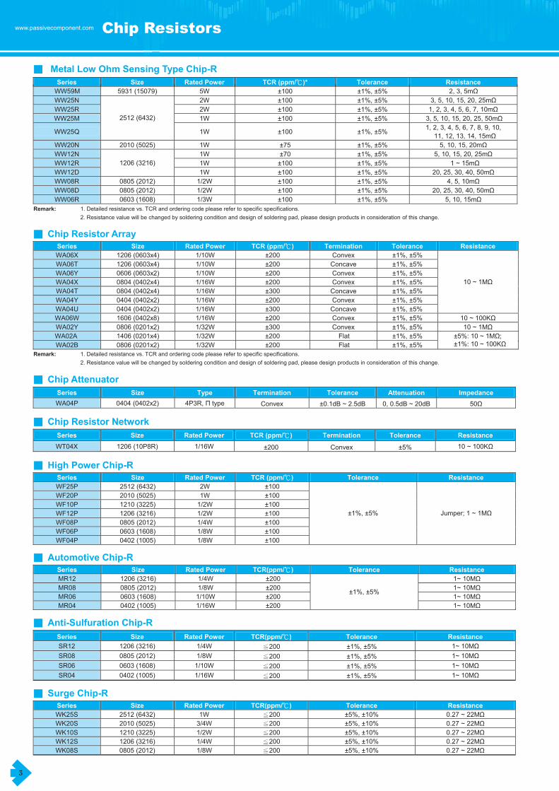
General Purpose Chip-R
Series Size Rated Power TCR (ppm/ )* Tolerance Resistance
±100 ±1%WR25X 2512 (6432) 1W
±200 ±5%
±100 ±1%WR18X 1218 (3248) 1W
±200 ±5%
±100 ±1%WR20X 2010 (5025) 1/2W
±200 ±5%
±100 ±1%WR10X 1210 (3225) 1/3W
±200 ±5%
±100±1%
WR12X 1206 (3216) 1/4W±5%
±100±1%
WR08X 0805 (2012) 1/8W±5%
±100±1%
WR06X 0603 (1608) 1/10W±5%
±100±1%
WR04X 0402 (1005) 1/16W±5%
±200 ±1%WR02X 0201 (0603) 1/20W
±200 ±5%
1 ~ 10M
±200 ±1%WR01X 01005 (0402) 1/32W
±200 ±5%4.7 ~ 1M
Remark: 1. Detailed resistance vs. TCR and ordering code please refer to specific specifications.
2. Jumper resistor is not designed for fusing applications, designers shall apply dedicate fusible resistor or standard fuse in
3. WRxxW defines for ±1% < 10ohm or > 1Mohm.
application circuits.
Thick Film Low Ohm Chip-R
Remark: 1. Detailed resistance vs. TCR and ordering code please refer to specific specifications.
2. Resistance value will be changed by soldering condition and design of soldering pad, please design products in consideration of this change.
Thick Film Power Low Ohm Chip-R
Series Size Rated Power TCR (ppm/ ) Tolerance Resistance
±1%, ±5% 0.047 ~ 0.976WW25P 2512 (6432) 2W< 0.1 : 150ppm
0.1 : 100ppm
0.047 ~ 0.976WW20P 2010 (5025) 1W< 0.1 : 150ppm
0.1 : 100ppm
0.020 ~ 0.976WW10P 1210 (3225) 1/2W< 0.1 : 500ppm
0.1 : 200ppm
0.020 ~ 0.976WW12P 1206 (3216) 1/2W< 0.1 : 200ppm
0.1 : 100ppm
0.047 ~ 0.976WW08P 0805 (2012) 1/3W< 0.1 : 200ppm
0.1 : 150ppm
0.047 ~ 0.976WW06P 0603 (1608) 1/4W< 0.1 : 250ppm
0.1 : 200ppm
0.100 ~ 0.976WW04P 0402 (1005) 1/8W< 0.1 : 300ppm
0.1 : 200ppm
< 0.02 : 150ppmWW12C 1206 (3216) 1/2W
0.02 : 100ppm
WW08C 0805 (2012) 1/3W
WW06C 0603 (1608) 1/4W
WW04C 0402 (1005) 1/8W
< 0.03 : 200ppm
0.03 : 100ppm
< 0.033 : 500ppm
0.051 : 100ppm
WW02C 0201 (0603) 1/10W < 0.051 : 300ppm
< 0.051 : 0~+250ppm
0.051 : ±150ppm
< 0.051 : 0~+350ppm
0.051 : ±150ppm
±1%, ±5%
±1%, ±5%
±1%, ±5%
±1%, ±5%
±1%, ±5%
±1%, ±5%
±1%, ±5%
±1%, ±5%
±1%, ±5%
±1%, ±5%
±1%, ±5%
Series Size Rated Power TCR (ppm/ ) Tolerance Resistance
0.015 ~ 0.976WW25XWW25W
2512 (6432) 1W0.010 ~ 0.100
±1% 0.020 ~ 0.976WW18X 1218 (3248) 1W
±5% 0.015 ~ 0.976
0.020 ~ 0.9762010 (5025)
0.010 ~ 0.100
0.100 ~ 0.9761210 (3225)
0.030 ~ 0.100
0.020 ~ 0.9761206 (3216)
0.010 ~ 0.100
0.020 ~ 0.9760805 (2012) 1/8W
0.050 ~ 0.100
0.100 ~ 0.9760603 (1608) 1/10W
0.050 ~ 0.100
WW04X 0402 (1005) 1/16W
WW20XWW20W
WW10XWW10W
1/3W2/3W
WW12XWW12W
WW08XWW08W
WW06XWW06W
1/4W1/3W
1/2W3/4W
3
Chip Resistorswww.passivecomponent.com
Chip Resistor Array
Series Size Rated Power TCR (ppm/ ) Termination Tolerance Resistance
WA06X 1206 (0603x4) 1/10W ±200 Convex ±1%, ±5%
WA06T 1206 (0603x4) 1/10W ±200 Concave ±1%, ±5%
WA06Y 0606 (0603x2) 1/10W ±200 Convex ±1%, ±5%
WA04X 0804 (0402x4) 1/16W ±200 Convex ±1%, ±5%
WA04T 0804 (0402x4) 1/16W ±300 Concave ±1%, ±5%
WA04Y 0404 (0402x2) 1/16W ±200 Convex ±1%, ±5%
WA04U 0404 (0402x2) 1/16W ±300 Concave ±1%, ±5%
10 ~ 1M
WA06W 1606 (0402x8) 1/16W ±200 Convex ±1%, ±5% 10 ~ 100K
WA02Y 0806 (0201x2) 1/32W ±300 Convex ±1%, ±5% 10 ~ 1M
WA02A 1406 (0201x4) 1/32W ±200 Flat
Flat
±1%, ±5%
WA02B 0806 (0201x2) 1/32W ±200 ±1%, ±5%
Remark: 1. Detailed resistance vs. TCR and ordering code please refer to specific specifications.
2. Resistance value will be changed by soldering condition and design of soldering pad, please design products in consideration of this change.
Chip Attenuator
Series Size Type Termination Tolerance Attenuation Impedance
WA04P 0404 (0402x2) 4P3R, type Convex ±0.1dB ~ 2.5dB 0, 0.5dB ~ 20dB 50
Chip Resistor Network
Series Size Rated Power TCR (ppm/ ) Termination Tolerance Resistance
WT04X 1206 (10P8R) 1/16W ±200 Convex ±5% 10 ~ 100K
High Power Chip-R
Series Size Rated Power TCR (ppm/ ) Tolerance Resistance
WF25P 2512 (6432) 2W ±100
WF20P 2010 (5025) 1W ±100
WF10P 1210 (3225) 1/2W ±100
WF12P 1206 (3216) 1/2W ±100
WF08P 0805 (2012) 1/4W ±100
WF06P 0603 (1608) 1/8W ±100
WF04P 0402 (1005) 1/8W ±100
±1%, ±5% Jumper 1 ~ 1M
Automotive Chip-R
Series Size Rated Power TCR(ppm/ ) Tolerance Resistance
MR12 1206 (3216) 1/4W ±200 1~ 10M
MR08 0805 (2012) 1/8W ±200 1~ 10M
MR06 0603 (1608) 1/10W ±200 1~ 10M
MR04 0402 (1005) 1/16W ±200
±1%, ±5%
1~ 10M
Anti-Sulfuration Chip-R
Series Size Rated Power TCR(ppm/ ) Tolerance Resistance
SR12 1206 (3216) 1/4W 200 ±1%, ±5% 1~ 10M
SR08 0805 (2012) 1/8W 200 ±1%, ±5% 1~ 10M
SR06 0603 (1608) 1/10W 200 ±1%, ±5% 1~ 10M
SR04 0402 (1005) 1/16W 200 ±1%, ±5% 1~ 10M
Surge Chip-R
Series Size Rated Power TCR(ppm/ ) Tolerance Resistance
WK25S 2512 (6432) 1W 200 ±5%, ±10% 0.27 ~ 22M
WK20S 2010 (5025) 3/4W 200 ±5%, ±10% 0.27 ~ 22M
WK10S 1210 (3225) 1/2W 200 ±5%, ±10% 0.27 ~ 22M
WK12S 1206 (3216) 1/4W 200 ±5%, ±10% 0.27 ~ 22M
WK08S 0805 (2012) 1/8W 200 ±5%, ±10% 0.27 ~ 22M
Metal Low Ohm Sensing Type Chip-R
Series Size Rated Power TCR (ppm/ )* Tolerance Resistance
WW25N 2W ±100 ±1%, ±5%
WW25R 2W ±100 ±1%, ±5% 1, 2, 3, 4, 5, 6, 7, 10m
WW25M 1W ±100 ±1%, ±5% 3, 5, 10, 15, 20, 25, 50m
3, 5, 10, 15, 20, 25m
WW25Q
2512 (6432)
1W ±100 ±1%, ±5%1, 2, 3, 4, 5, 6, 7, 8, 9, 10,
11, 12, 13, 14, 15m
WW20N 2010 (5025) 1W ±75 ±1%, ±5% 5, 10, 15, 20m
WW59M 5931 (15079) 5W ±100 ±1%, ±5%
WW12N 1W ±70 ±1%, ±5% 5, 10, 15, 20, 25m
WW12R 1W ±100 ±1%, ±5% 1 ~ 15
WW12D
1206 (3216)
1W ±100 ±1%, ±5% 20, 25, 30, 40, 50m
WW08R 0805 (2012) 1/2W ±100 ±1%, ±5% 4, 5, 10m
WW08D 0805 (2012) 1/2W ±100 ±1%, ±5% 20, 25, 30, 40, 50m
WW06R 0603 (1608) 1/3W ±100 ±1%, ±5% 5, 10, 15m
Remark: 1. Detailed resistance vs. TCR and ordering code please refer to specific specifications.
2. Resistance value will be changed by soldering condition and design of soldering pad, please design products in consideration of this change.

4
www.passivecomponent.com
Chip Resistors
High Voltage Chip-RSeries Size Rated Power TCR(ppm/ ) Voltage (V) Tolerance Resistance
WK25Z 2512 (6432) 1W 200 2000 ±5%, ±10%, ±20% 4.7M ~ 16M
WK20Z 2010 (5025) 1/2W 200 1500 ±5%, ±10%, ±20% 1M ~ 16M
WK25V 2512 (6432) 1W 200 800 ±1%, ±5% 47~ 51M
WK20V 2010 (5025) 1/2W 200 500 ±1%, ±5% 47~ 51M
WK12V 1206 (3216) 1/4W 200 500 ±1%, ±5% 47~ 51M
WK08V 0805 (2012) 1/8W 200 400 ±1%, ±5% 47~ 51M
WK06V 0603 (1608) 1/10W 200 200 ±1%, ±5% 47~ 10M
Trimmable Chip-RSeries Size Rated Power TCR(ppm/ ) Tolerance Resistance
WK25M 2512 (6432) 1W 200 0/-20%, 0/-30% 1 ~ 4.7M
WK20M 2010 (5025) 1/2W 200 0/-20%, 0/-30% 1 ~ 4.7M
WK10M 1210 (3225) 1/4W 200 0/-20%, 0/-30% 1 ~ 4.7M
WK12M 1206 (3216) 1/8W 200 0/-20%, 0/-30% 1 ~ 4.7M
WK08M 0805 (2012) 1/10W 200 0/-20%, 0/-30% 1 ~ 4.7M
WK06M 0603 (1608) 1/16W 100 0/-20%, 0/-30% 10~ 4.7M
Total lead free Chip-R ( Pb < 100ppm )Series Size Rated Power TCR(ppm/ ) Tolerance Resistance
WR12X_R 1206 (3216) 1/4W 200 ±1%, ±5% 1~ 10M
WR06X_R 0603 (1608) 1/10W 200 ±1%, ±5% 1~ 10M
WR04X_R 0402 (1005) 1/16W 200 ±1%, ±5% 1~ 10M
WR02X_R 0201 (0603) 1/20W 200 ±1%, ±5% 1~ 10M
WA04X_R 0402X4 1/16W 200 ±1%, ±5% 10 ~ 1M
WA06X_R 0603X4 1/10W 200 ±1%, ±5% 10 ~ 1M
High Precision Chip-RSeries Size Rated Power TCR(ppm/ ) Tolerance Resistance
WF12H 1206 (3216) 1/4W 100 ±0.1%, ±0.5% 10 ~ 1M
WF10H 1210 (3225) 1/3W 100 ±0.1%, ±0.5% 10 ~ 1M
WF08H 0805 (2012) 1/8W 100 ±0.1%, ±0.5% 10 ~ 1M
WF06H 0603 (1608) 1/10W 100 ±0.1%, ±0.5% 10 ~ 1M
WF04H 0402 (1005) 1/16W 100 ±0.1%, ±0.5% 10 ~ 1M
WF25T 2512 (6432) 3/4W 50 ±0.05%, ±0.10%,±0.25%, ±0.50%, ±1.0% 10 ~ 1.5M
WF25Q 2512 (6432) 1W 50 ±0.05%, ±0.10%,±0.25%, ±0.50%, ±1.0% 10 ~ 1.5M
WF20T 2010 (5025) 1/2W 50 ±0.05%, ±0.10%,±0.25%, ±0.50%, ±1.0% 10 ~ 1.5M
WF20Q 2010 (5025) 3/4W 50 ±0.05%, ±0.10%,±0.25%, ±0.50%, ±1.0% 10 ~ 1.5M
WF10T 1210 (3225) 1/4W 50 ±0.05%, ±0.10%,±0.25%, ±0.50%, ±1.0% 10 ~ 1M
WF10Q 1210 (3225) 2/5W 50 ±0.05%, ±0.10%,±0.25%, ±0.50%, ±1.0% 10 ~ 1M
WF12T 1206 (3216) 1/8W 50 ±0.05%, ±0.10%,±0.25%, ±0.50%, ±1.0% 4.7 ~ 1M
WF12Q 1206 (3216) 1/4W 50 ±0.05%, ±0.10%,±0.25%, ±0.50%, ±1.0% 4.7 ~ 1M
WF08T 0805 (2012) 1/10W 50 ±0.05%, ±0.10%,±0.25%, ±0.50%, ±1.0% 4.7 ~ 1M
WF08Q 0805 (2012) 1/8W 50 ±0.05%, ±0.10%,±0.25%, ±0.50%, ±1.0% 4.7 ~ 1M
WF06T 0603 (1608) 1/16W 50 ±0.05%, ±0.10%,±0.25%, ±0.50%, ±1.0% 4.7 ~ 680K
WF06Q 0603 (1608) 1/10W 50 ±0.05%, ±0.10%,±0.25%, ±0.50%, ±1.0% 4.7 ~ 680K
WF04T 0402 (1005) 1/16W 50 ±0.05%, ±0.10%,±0.25%, ±0.50%, ±1.0% 10 ~ 100K
WF25U 2512 (6432) 3/4W 25 ±0.05%, ±0.10%,±0.25%, ±0.50%, ±1.0% 10 ~ 1.5M
WF25R 2512 (6432) 1W 25 ±0.05%, ±0.10%,±0.25%, ±0.50%, ±1.0% 10 ~ 1.5M
WF20U 2010 (5025) 1/2W 25 ±0.05%, ±0.10%,±0.25%, ±0.50%, ±1.0% 10 ~ 1.5M
WF20R 2010 (5025) 3/4W 25 ±0.05%, ±0.10%,±0.25%, ±0.50%, ±1.0% 10 ~ 1.5M
WF10U 1210 (3225) 1/4W 25 ±0.05%, ±0.10%,±0.25%, ±0.50%, ±1.0% 10 ~ 1M
WF10R 1210 (3225) 2/5W 25 ±0.05%, ±0.10%,±0.25%, ±0.50%, ±1.0% 10 ~ 1M
WF12U 1206 (3216) 1/8W 25 ±0.05%, ±0.10%,±0.25%, ±0.50%, ±1.0% 4.7 ~ 1M
WF12R 1206 (3216) 1/4W 25 ±0.05%, ±0.10%,±0.25%, ±0.50%, ±1.0% 4.7 ~ 1M
WF08U 0805 (2012) 1/10W 25 ±0.05%, ±0.10%,±0.25%, ±0.50%, ±1.0% 4.7 ~ 1M
WF08R 0805 (2012) 1/8W 25 ±0.05%, ±0.10%,±0.25%, ±0.50%, ±1.0% 4.7 ~ 1M
WF06U 0603 (1608) 1/16W 25 ±0.05%, ±0.10%,±0.25%, ±0.50%, ±1.0% 4.7 ~ 680K
WF06R 0603 (1608) 1/10W 25 ±0.05%, ±0.10%,±0.25%, ±0.50%, ±1.0% 4.7 ~ 680K
WF04U 0402 (1005) 1/16W 25 ±0.05%, ±0.10%,±0.25%, ±0.50%, ±1.0% 10 ~ 100K
WF12F 1206 (3216) 1/8W 15 ±0.05%, ±0.10%,±0.25%
WF08F 0805 (2012) 1/8W 15 ±0.05%, ±0.10%,±0.25%
WF06F 0603 (1608) 1/10W 15 ±0.05%, ±0.10%,±0.25%
WF04F 0402 (1005) 1/16W 15 ±0.05%, ±0.10%,±0.25%
WF12W 1206 (3216) 1/8W 10 ±0.05%, ±0.10%,±0.25% 25 ~ 300K
WF08W 0805 (2012) 1/8W 10 ±0.05%, ±0.10%,±0.25% 25 ~ 200K
WF06W 0603 (1608) 1/10W 10 ±0.05%, ±0.10%,±0.25% 25 ~ 100K
WF04W 0402 (1005) 1/16W 10 ±0.05%, ±0.10%,±0.25% 25 ~ 20K
WF12Z 1206 (3216) 1/8W 5 ±0.05%, ±0.10%,±0.25% 25 ~ 120K
WF08Z 0805 (2012) 1/8W 5 ±0.05%, ±0.10%,±0.25% 25 ~ 80K
WF06Z 0603 (1608) 1/10W 5 ±0.05%, ±0.10%,±0.25% 25 ~ 40K
WF04Z 0402 (1005) 1/16W 5 ±0.05%, ±0.10%,±0.25% 25 ~ 8K
High Ohm Chip-RSeries Size Rated Power TCR(ppm/ ) Tolerance Resistance
WF12G 1206 (3216)
0805 (2012)
0603 (1608)
0402 (1005)
1/4W 200
1/8W 200
1/10W 200 ±1%, ±5%
±1%, ±5%
±1%, ±5%
1/16W 300 ±5%
WF08G
WF06G
WF04G
WR08X_R 0805 (2012) 1/8W 200 ±1%, ±5% 1~ 10M
WR10X_R 1210 (3225) 1/3W 200 ±1%, ±5% 1~ 10M

5
Chip Resistorswww.passivecomponent.com
-55 ~ +125 C-55 ~ +155 C

6
Chip Resistorswww.passivecomponent.com
Thick Film Low Ohm/Power Low Ohm Chip Resistors
Function For Low Ohm Chip Resistors
The low ohmic resistors are used to sense output current in power supply,automotive and engine control management system, and other powersensing application. As shows in figure below, the typical function of lowohmic (power) chip resistor is to be a current sensor (Rsense) to generatethe sensing voltage (Vs) for the purpose of feedback control when outputcurrent (lo) passed on it . The sensing voltage be treated as a signal totrigger the switches (CMOS) ON/OFF duration so that to monitor and/oradjust the output current from inductor.Simplify to say, Vs=Io ×Rsense.In general case, this feedback voltage is setting around 100mV forconsidering both on power saving and noise robustness. To sense a 5ampere average output current, the Rsense resistance value therefore berequired as 100mV / 5A = 20 m , the power dissipation will be : P=I2 ×R =5A2 ×20m =0.5WattA low ohmic chip resistor with a power rating of 1.0 watt is recommendedon this application in case the power safety margin is taken into account.
Quick Reference Data of Low Ohm Chip Resistor
Series No. WW25X WW20X WW18X WW10X WW12X WW08X WW06X WW04X
Size code2512
(6432)
2010
(5025)
1218
(3248)
1210
(3225)
1206
(3216)
0805
(2012)
0603
(1608)
0402
(1005)
Resistance Tolerance ±5% , ±1%
Resistance Range 0.020 ~ 0.976 0.100 ~ 0.976
TCR (ppm/ ) Detailed TCR please refer to specific data sheets
Max. dissipation @ Tamb=70 1 Watt 0.5 Watt 1 Watt 1/3 Watt 1/4 Watt 1/8 Watt 1/10 Watt 1/16 Watt
Max. Operation Voltage (DC or RMS) 250V 200V 200V 200V 200V 100V 50V 50V
Operation Temperature
Basic Specification JIS C 5201-1 / IEC 60115-1
Note :
1. This is the maximum voltage that may be continuously supplied to the resistor element, see “IEC publication 60115-9” .2. Power derating curve, and detail specification please refer to specific data sheets.3. Resistance value will be changed by soldering condition and design of solding pad, please design products in consideration of change of resistance value.
Quick Reference Data of Power Low Ohm Chip Resistor
Item General Specification
Series No. WW25P WW20P WW12P WW08P WW06P WW04P
Size code 2512 (6432) 2010 (5025) 1206 (3216) 0805(2012) 0603(1608) 0402(1005)
Resistance Tolerance ±5% , ±1%
Resistance Range 0.047 ~ 0.976 0.1 ~0.976
TCR (ppm/ ) 0.100 ±150ppm/ ±150ppm/ ±200ppm/ ±200ppm/ ±250ppm/ -
0.100 ±100ppm/ ±100ppm/ ±100ppm/ ±150ppm/ ±200ppm/ 0~+300ppm/
Max. dissipation @ Tamb=70 2 W 1 W 1/2 W 1/3 W 1/4 W 1/8 W
Max. Operation Voltage (DC or RMS) 300V 200V 200V 150V 50V 50V
Operation Temperature
Note :1. This is the maximum voltage that may be continuously supplied to the resistor element, see “IEC publication 60115-8” .2. Max. Operation Voltage : So called RCWW (Rated Continuous Working Voltage) is determined by RCWV= Rater Power ×Resistance Value or Max. RCWV listed above, whichever is lower.3. 2W loading with total solder-pad and trace size of 300mm2
Physical Dimensions
Unit: mm
Dimensions WW25P WW20P WW12P WW08P WW06P WW04P
L 6.30±0.20 5.00±0.20 3.10±0.15 2.00±0.15 1.60±0.10 1.00±0.05
W 3.10±0.20 2.50±0.20 1.60±0.15 1.20±0.15 0.80±0.10 0.50±0.05
T 0.60±0.15 0.60±0.10 0.55±0.10 0.50±0.10 0.45±0.10 0.35±0.05
Tt 0.60±0.25 0.60±0.25 0.50±0.25 0.40±0.20 0.30±0.20 0.20±0.10
Tb 1.80±0.25 0.65±0.25 0.50±0.25 0.40±0.20 0.30±0.20 0.25+0.05/-0.1
-55 ~ +155 C
-55 ~ +155 C

7
Chip Resistorswww.passivecomponent.com
Metal Low Ohm Sensing Chip Resistors (0.001 ~ 0.050 )
Description
The resistors are constructed in a high grade low resistive metal body. The resistivelayer is covered with a protective coat and printed a resistance marking code over it.Finally, the two external end terminations are added. For ease of soldering the outerlayer of these end terminations is a lead free terminations.
Quick Reference Data
Item General Specification
Series No. WW25M WW25N WW20M WW20N WW12N WW12M
Size code 2512 (6432) 2010 (5025) 1206(3216)
Resistance Tolerance ±5% , ±1%
Resistance Range1~10, 12, 15, 20,
25, 30, 40, 50m
1~10, 12, 15, 20,
25m5, 10, 15, 20m 5, 10, 15, 20, 25m
TCR (ppm/ ) 1-4m : ±100ppm; > 4m: ± 75 ppm/ ± 75 ppm/ ± 70 ppm/
Max. dissipation @ Tamb=70 1 W 2 W 1/2 W 1 W 1 W 1/2 W
Max. Operation Voltage (DC or RMS) 250V 250V 200V
Max. Overload Voltage (DC or RMS) 500V 500V 400V
Operation Temperature
Note :1. This is the maximum voltage that may be continuously supplied to the resistor element, see “IEC publication 60115-8” .2. Power derating curve, and detail specification please refer to specific data sheets.3. Resistance value will be changed by soldering condition and design of solding pad, please design products in consideration of chang of resistance value.
Physical Dimensions:
WW25M(0.002 ~0.025 ), WW25N(0.003 ~0.025 ), WW20N, WW12N
Unit: mm
WW25M(0.001 ), WW25N(0.001 ~0.002 )
Unit: mm
Symbol 2512
L 6.40±0.20
W 3.20±0.20
T 0.60±0.10
Tt 1.60±0.25
Tb 1.60±0.25
WW25Q, WW25R, WW12R, WW12D, WW06R
Note : 1. The detailed dimensions please refer to data sheet per type!
Symbol 2512 2010 1206
L 6.40±0.20 5.00±0.20 3.10±0.20
W 3.20±0.20 2.50±0.20 1.60±0.20
T 0.60±0.15 0.60±0.15 0.60±0.25
Tt 0.65±0.25 0.65±0.25 0.60±0.20
Tb 0.65±0.25 0.65±0.25 0.60±0.20
-55 ~ +155 C
Item General Specification
Series No. WW25R WW25Q WW12R WW12D WW08R WW06R
Size code 2512 (6432) 1206(3216) 0805 (2012) 0603 (1608)
Resistance Tolerance ±5% , ±1%
Resistance Range1,2,3,4,
1 ~ 15m 1 ~ 15m20, 25, 30, 40,
50m
20, 25, 30, 40
50m5, 10, 15m
TCR (ppm/ ) ±100ppm ±100ppm ±100ppm ±100ppm
Max. dissipation @ Tamb=70 2 W 1 W 1 W 1 W 1/2 W 1/3 W
Max. Operation Current (DC or RMS) 44.7A 14A 5A 8.1A
Operation Temperature -55 ~ +155 C
WW08D
1/2 W
11A

8
Chip Resistorswww.passivecomponent.com
Chip Resistors Array : Convex Termination
Feature Application
1. High reliability and stability 1. Consumer electrical equipment, PDA Digital Camcorder,2. Reduced size of final equipment 2. EDP, Computer application3. Lower assembly cost and higher surface mounted efficiency 3. Mobile phone, Telecom4. Higher component and equipment reliability 4. DIMM
Description and Physical Dimensions
The resistors array is constructed in a high grade ceramic body (aluminum oxide). Internal metalelectrodes are added at each end and connected by a resistive paste that is applied to the topsurface of the substrate. The composition of the paste is adjusted to give the approximateresistance required and the value is trimmed to within tolerance by laser cutting of this resistivelayer.The resistive layer is covered with a protective coat. Finally, the two external end terminations areadded. For ease of soldering the outer layer of these end termination is Tin solder alloy. Markingcode description is depended on component size and tolerance. Following figure shown theconstruction of a Chip-R array.
Physical Dimensions Unit: mm
Type WA06X WA04X WA06Y WA04Y
L 3.20±0.10 2.00±0.10 1.60±0.10 1.00±0.10
W 1.60±0.10 1.00±0.10 1.50±0.10 1.00±0.10
T 0.50±0.10 0.45±0.10 0.50±0.10 0.35±0.10
P 0.80±0.10 0.50±0.05 1.00±0.10 0.65±0.10
A 0.60±0.10 0.40±0.10 0.60±0.10 0.34±0.10
B 0.30±0.10 0.20±0.10 0.30±0.15 0.20±0.15
C 0.40±0.10 0.30±0.05 - -
G 0.30±0.20 0.25±0.10 0.30±0.15 0.25±0.17
Quick Reference Data
Series No. WA06X WA04X WA06Y WA04Y
Size 0603×4(1608×4) 0402×4(1005×4) 0603×2(1608×4) 0402×2(1005×2)
Termination construction 8P4R,Convex 4P2R,Convex
Resistance Tolerance ±5%, ±1% (E24 series)
Resistance Range 10 ~1M (E24 series), Jumper (0 )
TCR (ppm/ ) ±200 ppm/
Max. dissipation @ Tamb=70 1/10 Watt 1/16 Watt 1/10 Watt 1/16 Watt
Max. Operation Voltage (DC or RMS) 50V 50V
Max. Overload Voltage (DC or RMS) 100V 100V
50V
100V
25V
50V
Operation Temperature
Basic Specification JIS C5201-1 / IEC 60115-1
Circuit Mode: R1=R2(=R3=R4)
Note :Power derating curve and detail specification please refer to specific data sheets.
-55 ~ +155 C

9
Chip Resistorswww.passivecomponent.com
WA06W Chip Resistors Array 16P8R
Description
The resistors array is constructed in a high grade ceramic body (aluminum oxide).Internal metal electrodes are added at each end and connected by a resistive paste thatis applied to the top surface of the substrate. The composition of the paste is adjusted togive the approximate resistance required and the value is trimmed to within tolerance bylaser cutting of this resistive layer.The resistors layer is covered with a protective coat. Finally, the two external endterminations are added. For ease of soldering the outer layer of these end termination isTin (Pb free) solder alloy.
Quick Reference Data
Item General Specification
Series No. WA06W WA06W_N
Size 1606 (0602×8) 1606 (0602×8)
Termination construction Convex type Convex type
Resistance Tolerance ±5% (E24 series) ±5% (E24 series)
Resistance Range 10 ~100K , Jumper (0 ) 10 ~100K , Jumper (0 )
TCR (ppm/ ) ± 200 ppm/ ± 200 ppm/
Max. dissipation @ Tamb=70 1/16 W 1/16 W
Max. Operation Voltage (DC or RMS) 50V 25V
Max. Overload Voltage (DC or RMS) 100V 50V
Carrier Tape width 12mm 8mm
Operation Temperature
Circuit Mode:
R1=R2=R3=R4=R5=R6=R7=R8
Note :Power derating curve and detail specification please refer to specific data sheets.
Physical Dimensions: Unit: mm
Symbol WA06W WA06W_N
L 4.00±0.20 3.80±0.10
W 1.60±0.15 1.60±0.10
T 0.45±0.10 0.45±0.10
B 0.30±0.20 0.30±0.10
G 0.30±0.20 0.30±0.10
D 0.20±0.10 0.20±0.10
P 0.50±0.20 0.50±0.10
H1 0.40±0.20 0.30±0.10
H2 0.30±0.10 0.30±0.10
-55 ~ +155 C

10
Chip Resistorswww.passivecomponent.com
Chip Resistors Array : Concave Termination
Feature Application
1. High reliability and stability 1. Consumer electrical equipment, PDA Digital Camcorder,2. Reduced size of final equipment 2. EDP, Computer application3. Lower assembly cost and higher surface mounted efficiency 3. Mobile phone, Telecom4. Higher component and equipment reliability 4. DIMM5. Strong body and terminations6. Excellent performance in surface mounting assembly.
Description and Physical Dimensions
The resistor array is constructed in a high grade ceramic body (aluminum oxide).Internal metal electrodes are added at each end and connected by a resistivepaste that is applied to the top surface of the substrate. The composition of thepaste is adjusted to give the approximate resistance required and the value istrimmed to within tolerance by laser cutting of this resistive layer.The resistive layer is covered with a protective coat. Finally, the two external endterminations are added. For ease of soldering the outer layer of these endtermination is Tin solder alloy. Marking code description is depended oncomponent size and tolerance. Following figure shown the construction of aChip-R array.
Quick Reference Data
Item General Specification
Series No. WA06T WA04T WA04U
Size 0603×4 (1608×4) 0402×4 (1005×4) 0402×2 (1005×2)
Termination construction Concave type
Resistance Tolerance ±5% , ±1% (E24 series)
Resistance Range 10 ~1M , Jumper (0 )
TCR (ppm/ ) ± 200 ppm/ ± 300 ppm/ ± 300 ppm/
Max. dissipation @ Tamb=70 1/10 W 1/16 W 1/16 W
Max. Operation Voltage (DC or RMS) 50V 25V 25V
Max. Overload Voltage 100V 50V 50V
Operation Temperature
Circuit Mode
L 3.20+0.20/-0.10mm 2.00±0.10mm 1.00±0.10mm
W 1.60+0.20/-0.10mm 1.00±0.10mm 1.00±0.10mm
T 0.60±0.20mm 0.45±0.10mm 0.30±0.10mm
P 0.80±0.10mm 0.50±0.05mm 0.50±0.05mm
A 0.60±0.15mm 0.35±0.05mm 0.35±0.10mm
B 0.35±0.15mm 0.20±0.15mm 0.25±0.15mm
C 0.50±0.15mm 0.25±0.05mm 0.35±0.10mm
G 0.50±0.15mm 0.25±0.15mm 0.25±0.15mm
Note :1. Power derating curve and detail specification please refer to specific data sheets.2. Max. Operation Voltage : So called RCWW (Rated Continuous Working Voltage) is determined byRCWV = Rater Power × Resistance Value or Max. RCWV listed above, whichever is lower.
-55 ~ +155 C
11
Chip Resistorswww.passivecomponent.com
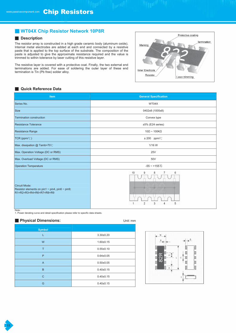
WT04X Chip Resistor Network 10P8R
Description
The resistor array is constructed in a high grade ceramic body (aluminum oxide).Internal metal electrodes are added at each end and connected by a resistivepaste that is applied to the top surface of the substrate. The composition of thepaste is adjusted to give the approximate resistance required and the value istrimmed to within tolerance by laser cutting of this resistive layer.
The resistive layer is covered with a protective coat. Finally, the two external endterminations are added. For ease of soldering the outer layer of these endtermination is Tin (Pb free) solder alloy.
Quick Reference Data
Item General Specification
Series No. WT04X
Size 0402x8 (1005x8)
Termination construction Convex type
Resistance Tolerance ±5% (E24 series)
Resistance Range 10 ~ 100K
TCR (ppm/ ) ± 200 ppm/
Max. dissipation @ Tamb=70 1/16 W
Max. Operation Voltage (DC or RMS) 25V
Max. Overload Voltage (DC or RMS) 50V
Operation Temperature
Circuit Mode:
Resistor elements on pin1 ~ pin4, pin6 ~ pin9;
R1=R2=R3=R4=R6=R7=R8=R9
Note :1. Power derating curve and detail specification please refer to specific data sheets.
Physical Dimensions: Unit: mm
Symbol
L 3.30±0.20
W 1.60±0.15
T 0.55±0.10
P 0.64±0.05
A 0.50±0.05
B 0.40±0.15
C 0.40±0.15
G 0.40±0.15
-55 ~ +155 C
12
www.passivecomponent.com
Chip Resistors
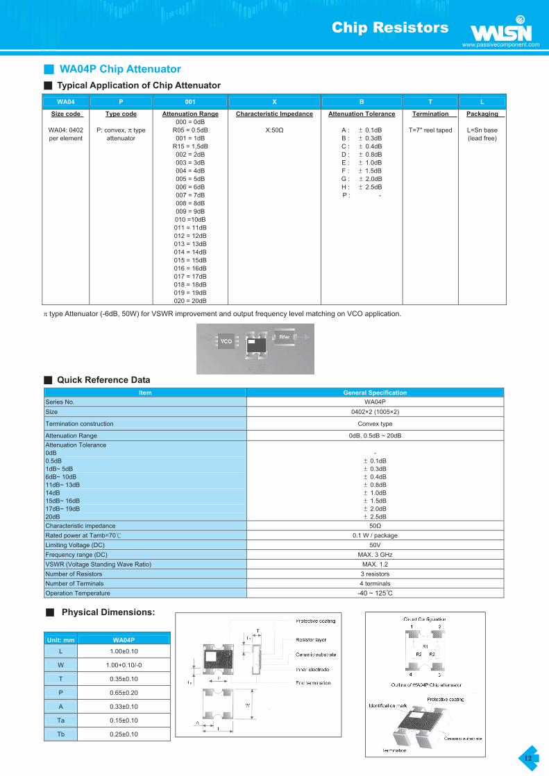
Physical Dimensions:
Unit: mm WA04P
L 1.00±0.10
W 1.00+0.10/-0
T 0.35±0.10
P 0.65±0.20
A 0.33±0.10
Ta 0.15±0.10
Tb 0.25±0.10
WA04P Chip Attenuator
Typical Application of Chip Attenuator
WA04 P 001 X B T L
Size code
WA04: 0402
per element
Type code
P: convex, type
attenuator
Attenuation Range
000 = 0dB
R05 = 0.5dB
001 = 1dB
R15 = 1,5dB
002 = 2dB
003 = 3dB
004 = 4dB
005 = 5dB
006 = 6dB
007 = 7dB
008 = 8dB
009 = 9dB
010 =10dB
011 = 11dB
012 = 12dB
013 = 13dB
014 = 14dB
015 = 15dB
016 = 16dB
017 = 17dB
018 = 18dB
019 = 19dB
020 = 20dB
Characteristic Impedance
X:50
Attenuation Tolerance
A : 0.1dB
B : 0.3dB
C : 0.4dB
D : 0.8dB
E : 1.0dB
F : 1.5dB
G : 2.0dB
H : 2.5dB
P : -
Termination
T=7'' reel taped
Packaging
L=Sn base
(lead free)
type Attenuator (-6dB, 50W) for VSWR improvement and output frequency level matching on VCO application.
Quick Reference Data
Item General Specification
Series No. WA04P
Size 0402×2 (1005×2)
Termination construction Convex type
Attenuation Range 0dB, 0.5dB ~ 20dB
Attenuation Tolerance
0dB
0.5dB
1dB~ 5dB
6dB~ 10dB
11dB~ 13dB
14dB
15dB~ 16dB
17dB~ 19dB
20dB
-
0.1dB
0.3dB
0.4dB
0.8dB
1.0dB
1.5dB
2.0dB
2.5dB
Characteristic impedance 50
Rated power at Tamb=70 0.1 W / package
Limiting Voltage (DC) 50V
Frequency range (DC) MAX. 3 GHz
VSWR (Voltage Standing Wave Ratio) MAX. 1.2
Number of Resistors 3 resistors
Number of Terminals 4 terminals
Operation Temperature -40 ~ 125 C
13
Chip Resistorswww.passivecomponent.com
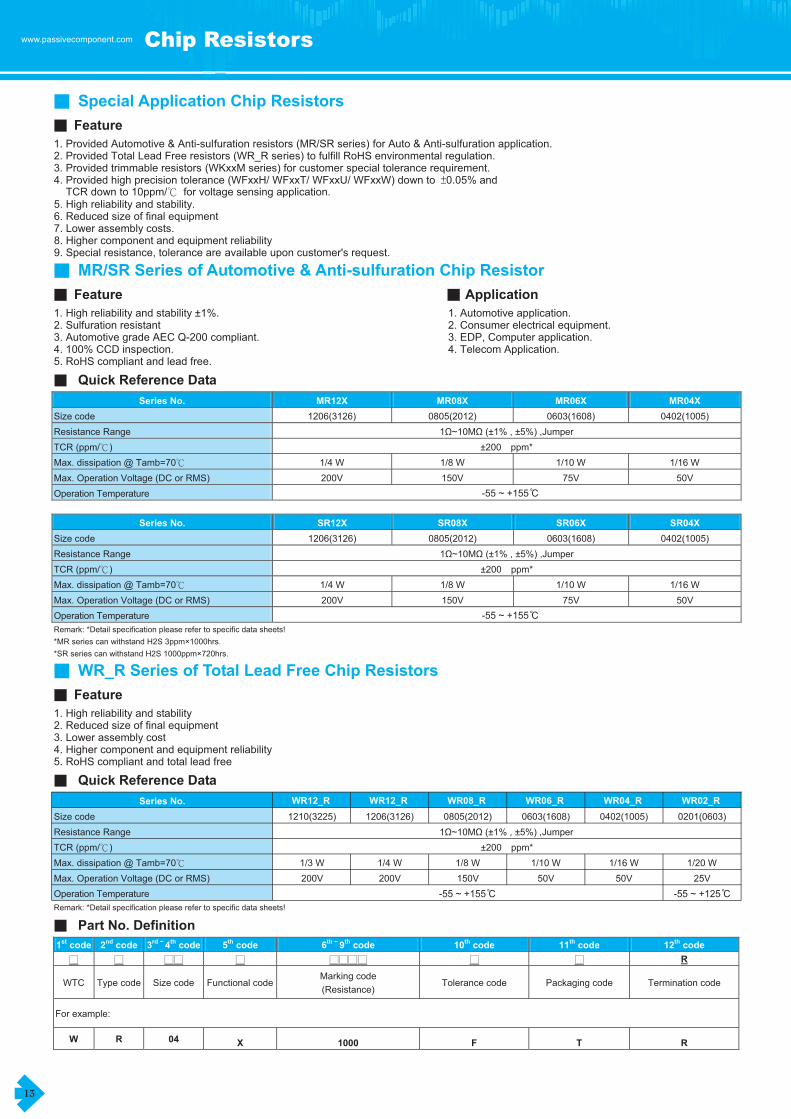
Special Application Chip Resistors
Feature
1. Provided Automotive & Anti-sulfuration resistors (MR/SR series) for Auto & Anti-sulfuration application.2. Provided Total Lead Free resistors (WR_R series) to fulfill RoHS environmental regulation.3. Provided trimmable resistors (WKxxM series) for customer special tolerance requirement.4. Provided high precision tolerance (WFxxH/ WFxxT/ WFxxU/ WFxxW) down to ±0.05% and
TCR down to 10ppm/ for voltage sensing application.5. High reliability and stability.6. Reduced size of final equipment7. Lower assembly costs.8. Higher component and equipment reliability9. Special resistance, tolerance are available upon customer's request.
MR/SR Series of Automotive & Anti-sulfuration Chip Resistor
Feature Application
1. High reliability and stability ±1%.2. Sulfuration resistant3. Automotive grade AEC Q-200 compliant.4. 100% CCD inspection.5. RoHS compliant and lead free.
1. Automotive application.2. Consumer electrical equipment.3. EDP, Computer application.4. Telecom Application.
Quick Reference Data
Series No. MR12X MR08X MR06X MR04X
Size code 1206(3126) 0805(2012) 0603(1608) 0402(1005)
Resistance Range 1 ~10M (±1% , ±5%) ,Jumper
TCR (ppm/ ) ±200 ppm*
Max. dissipation @ Tamb=70 1/4 W 1/8 W 1/10 W 1/16 W
Max. Operation Voltage (DC or RMS) 200V 150V 75V 50V
Operation Temperature
Series No. SR12X SR08X SR06X SR04X
Size code 1206(3126) 0805(2012) 0603(1608) 0402(1005)
Resistance Range 1 ~10M (±1% , ±5%) ,Jumper
TCR (ppm/ ) ±200 ppm*
Max. dissipation @ Tamb=70 1/4 W 1/8 W 1/10 W 1/16 W
Max. Operation Voltage (DC or RMS) 200V 150V 75V 50V
Operation Temperature
Remark: *Detail specification please refer to specific data sheets!
*MR series can withstand H2S 3ppm×1000hrs.
*SR series can withstand H2S 1000ppm×720hrs.
WR_R Series of Total Lead Free Chip Resistors
Feature
1. High reliability and stability2. Reduced size of final equipment3. Lower assembly cost4. Higher component and equipment reliability5. RoHS compliant and total lead free
Quick Reference Data
Part No. Definition
1st
code 2nd
code 3rd ~
4th
code 5th
code 6th ~
9th
code 10th
code 11th
code 12th
code
R
WTC Type code Size code Functional codeMarking code
(Resistance)Tolerance code Packaging code Termination code
For example:
W R 04 X 1000 F T R
-55 ~ +155 C
-55 ~ +155 C
Size code
Resistance Range 1 ~10M (±1% , ±5%) ,Jumper
TCR (ppm/ ) ±200 ppm*
Max. dissipation @ Tamb=70
Max. Operation Voltage (DC or RMS)
Operation Temperature
Remark: *Detail specification please refer to specific data sheets!
-55 ~ +155 C
1206(3126)
1/4 W
200V
WR12_R
1210(3225)
1/3 W
200V
WR12_R
0805(2012)
1/8 W
150V
WR08_R
0603(1608)
1/10 W
50V
WR06_R
0402(1005)
1/16 W
50V
WR04_R
0201(0603)
1/20 W
25V
WR02_R
-55 ~ +125 C
Series No.
14
www.passivecomponent.com
Chip Resistors
WKxxM Series of Trimmable Chip Resistors
Feature Application
1. High precision, reliability and stability2. Miniature size down to 00603 (1608)
1. Automotive application.2. Consumer electrical equipment.3. EDP, Computer application.4. Telecom Application.
Description
The resistive layer is covered with a transparent protective coat. Finally, the two external endterminations are added. For ease of soldering the outer layer of these end termination is Tin (Pbfree) solder alloy.
Physical Dimensions
Unit: mm
Type WK25M WK20M WK10M WK12M WK08M WK06M
L 6.30±0.15 5.00±0.15 3.10±0.15 3.10±0.15 2.00±0.10 1.60±0.10
W 3.20±0.15 2.50±0.15 2.50±0.15 1.60±0.15 1.25±0.10 0.80+0.15/-0.10
T 0.55±0.15 0.55±0.15 0.55±0.15 0.55±0.10 0.55±0.10 0.45±0.10
Tb 0.60±0.20 0.60±0.20 0.50±0.25 0.50±0.25 0.40±0.20 0.30±0.10
Tt 0.60±0.20 0.60±0.20 0.50±0.25 0.50±0.25 0.40±0.20 0.30±0.10
Quick Reference Data
Series No. WK25M WK20M WK10M WK12M WK08M WK06M
Size code 2512 (6332) 2010 (5025) 1210(3225) 1206(3216) 0805(2012) 0603(1608)
Resistance Tolerance 0/-20%(Y) and 0/-30%(X) E24 series
Resistance Range 1 ~ 4.7M 10 ~ 4.7M
TCR (ppm/ )10 ~ 4.7M : ±200 ppm/
1 ~ 9.1 : - 200 ~ +500 ppm/±200 ppm/
Max. dissipation @ Tamb=70 1 W 1/2 W 1/4 W 1/8 W 1/10 W 1/16 W
Max. Operation Voltage (DC or RMS) 200V 200V 200V 200V 150V 50V
Operation Temperature
Basic Specification JIS C 5201-1 / IEC 60115-1
WKxxV Series of High Voltage Chip Resistors
Feature Application
1. Special material and design for high working voltage required 2. Compatible with flow and reflow soldering.3. Suitable for lead free soldering.
1. Power supply.2. Automotive industry.3. Measurement instrument.4. Back light inverter.5. Medical or Military equipment
Quick Reference Data
Series No. WK25V WK20V WK12V WK08V WK06V
Size code 2512 (6332) 2010 (5025) 1206(3216) 0805(2012) 0603(1608)
Resistance Tolerance ±5% ; ±1%
Resistance Range 47 ~ 51M 47 ~ 10M
TCR (ppm/ ) ± 200 ppm/ * detail refer to data sheet
Max. dissipation @ Tamb=70 1 W 1/2 W 1/4 W 1/8 W 1/10 W
Max. Operation Voltage (DC or RMS) 800V 500V 500V 400V 200V
Operation Temperature
Note :
1. This is the maximum voltage that may be continuously supplied to the resistor element, see “IEC publication 60115-8” .
2. Max. Operation Voltage : So called RCWW (Rated Continuous Working Voltage) is determined
by RCWV= Rater Power ×Resistance Value or Max. RCWV listed above, whichever is lower.
Physical DimensionsUnit: mm
Symbol
L
W
T
Tt
Tb
-55 ~ +125 C
-55 ~ +125 C
WK25V
6.30±0.15
3.20±0.15
0.55±0.15
0.60±0.20
0.60±0.20
WK20V
5.00±0.15
2.50±0.15
0.55±0.15
0.60±0.20
0.60±0.20
WK12V
3.10±0.15
1.60±0.15
0.55±0.10
0.50±0.25
0.50±0.25
WK08V
2.00±0.10
1.25±0.10
0.55±0.10
0.40±0.20
0.40±0.20
WK06V
1.60±0.10
0.80+0.15/-0.10
0.45±0.10
0.30±0.10
0.30±0.10
The resistors are constructed on a high grade ceramic body (aluminum oxide). Internal metal electrodes are added at each end and connected by a resistive paste that is applied to the top surface of the substrate. The composition of the paste is adjusted to give the approximate resistance required.

15
Chip Resistorswww.passivecomponent.com
WFxxP Series of High Power Chip Resistors
Feature Application
1. High power rating and compact size2. High reliability and stability3. Reduced size of final equipment4. Lead free product is upon customer requested
1. Power supply2. PDA3. Digital meter4. Computer5. Automotives.
Quick Reference Data
Item General Specification
Series No. WF25P WF20P WF10P WF12P WF08P WF06P WF04P
Size code 2512(6432) 2010(5025) 1210(3225) 1206(3216) 0805(2012) 0603 (1608) 0402(1005)
Resistance Tolerance ±1% , ±5%
Resistance Range 0 , 1 ~ 1M
TCR (ppm/ ) ± 100 ppm/
Max. dissipation @ Tamb=70 2W 1W 1/2W 1/2W 1/4W 1/8W 1/8W
Max. Operation Voltage (DC or RMS) 300V 200V 200V 200V 150V 50V 50V
Operation Temperature
Note :
1. This is the maximum voltage that may be continuously supplied to the resistor element, see “IEC publication 60115-8”.
2. Max. Operation Voltage : So called RCWW (Rated Continuous Working Voltage) is determined by
RCWV= Rater Power ×Resistance Value or Max. RCWV listed above, whichever is lower.
3. 2W loading with total solder-pad and trace size of 300mm2
4. 0 maximum resistance Rmax 15m and rated current 4Amp
Physical Dimensions
Unit: mm
Symbol WF25P WF20P WF10P WF12P WF08P WF06P WF04P
L 6.30±0.20 5.00±0.20 3.10±0.10 3.10±0.15 2.00±0.15 1.60±0.10 1.00±0.05
W 3.10±0.20 2.50±0.20 2.60±0.10 1.60±0.15 1.20±0.15 0.80±0.10 0.50±0.05
T 0.60±0.15 0.60±0.10 0.55±0.10 0.55±0.10 0.50±0.10 0.45±0.10 0.35±0.05
Tt 0.60±0.25 0.60±0.25 0.50±0.20 0.50±0.25 0.40±0.20 0.30±0.20 0.25±0.10
Tb 1.80±0.25 0.60±0.25 0.50±0.20 0.50±0.25 0.40±0.20 0.30±0.20 0.25±0.10
WKxxS Series of Anti-Surge Chip Resistors
Feature Application
1. Power rating and compact size2. High reliability and stability3. Reduced size of final equipment4. Surge protection
1. Power supply.
2. Measurement instrument.
3. Automotive industry.
4. Medical or Military equipment.
Quick Reference Data
Item General Specification
Series No. WK25S WK20S WK10S WK12S WK08S
Size code 2512(6432) 2010(5025) 1210(3225) 1206(3216) 0805(2012)
Resistance Tolerance ±5% ,±10% ,±20%,(E24)
Resistance Range 0.27 ~ 22M
TCR (ppm/ ) ± 200 ppm/
Max. dissipation @ Tamb=70 1 W 3/4W 1/2W 1/4W 1/8W
Max. Operation Voltage (DC or RMS) 200V 150V
Operation Temperature
Note :
1. This is the maximum voltage that may be continuously supplied to the resistor element, see “IEC publication 60115-8” .
2. Max. Operation Voltage : So called RCWV (Rated Continuous Working Voltage) is determined by
RCWV= Rater Power ×Resistance Value or Max. RCWV listed above, whichever is lower.
Physical Dimensions
Unit: mm
Symbol WK25S WK20S WK10S WK12S WK08S
L 6.30±0.15 5.00±0.15 3.20±0.15 3.20±0.15 2.00±0.10
W 3.20±0.15 2.50±0.15 2.50±0.15 1.60±0.15 1.25±0.10
T 0.55±0.15 0.55±0.15 0.55±0.15 0.55±0.10 0.55±0.10
Tt 0.30±0.15 0.30±0.15 0.30±0.20 0.30±0.20 0.30±0.20
Tb 0.60±0.20 0.60±0.20 0.50±0.25 0.50±0.25 0.40±0.20
-55 ~ +155 C
-55 ~ +155 CDuration (msec)
Power( W
)
Pulse chart of WKxxS series
2512
2010
1210
1206
0805
Duration (msec)
Power( W
)
Pulse chart of WKxxS series
2512
2010
1210
1206
0805
16
www.passivecomponent.com
Chip Resistors
High Precision Chip Resistors
Narrow Tolerance Thick Film TC100 WFxxH SeriesSeries No. WF12H WF08H WF06H WF04H
Size 1206(3216) 0805(2012) 0603(1608) 0402(1005)
Resistance Tolerance ±0.5% , ±0.1%
Resistance Range 10 ~ 1M (E96+E24 series)
TCR (ppm/ ) ±100 ppm/
Max. dissipation @ Tamb=70 1/4 W 1/8 W 1/10 W 1/16 W
Max. Operation Voltage (DC or RMS) 200V 100V 50V 50V
Operation Temperature
Basic Specification JIS C5201-1 / IEC 60115-1
(Detail specification please refer to specific data sheets)
Narrow Tolerance Thin Film TC50 WFxxT/ WFxxQ SeriesSeries No. WF25T WF25Q WF20T WF20Q WF10T WF10Q WF12T WF12Q WF08T WF08Q WF06T WF06Q WF04T
Size2512
(6432)
2512
(6432)
2010
(5025)
2010
(5025)
1210
(3225)
1210
(3225)
1206
(3216)
1206
(3216)
0805
(2012)
0805
(2012)
0603
(1608)
0603
(1608)
0402
(1005)
Resistance Tolerance ±1%, ±0.5% , ±0.1%, ±0.05%
Resistance Range 10 ~ 1.5M 10 ~ 1M 4.7 ~ 1M 4.7 ~ 680K10 ~
100K
TCR (ppm/ ) ±50 ppm/
Max. dissipation @ Tamb=70 3/4W 1W 1/2W 3/4W 1/4W 2/5W 1/8W 1/4W 1/10W 1/8W 1/16W 1/10W 1/16W
Max. Operation Voltage (DC or RMS) 200V 200V 200V 200V 200V 200V 200V 200V 100V 150V 50V 75V 25V
Basic Specification JIS C5201-1 / IEC 60115-1
(Detail specification please refer to specific data sheets)
Narrow Tolerance Thin Film TC25 WFxxU/ WFxxR SeriesSeries No. WF25U WF25R WF20U WF20R WF10U WF10R WF12U WF12R WF08U WF08R WF06U WF06R WF04U
Size2512
(6432)
2512
(6432)
2010
(5025)
2010
(5025)
1210
(3225)
1210
(3225)
1206
(3216)
1206
(3216)
0805
(2012)
0805
(2012)
0603
(1608)
0603
(1608)
0402
(1005)
Resistance Tolerance ±1%, ±0.5% , ±0.1%, ±0.05%
Resistance Range10 ~ 1.5M 10 ~ 1M 4.7 ~ 1M 4.7 ~ 680K
10 ~
100K
TCR (ppm/ ) ±25 ppm/
Max. dissipation @ Tamb=70 3/4W 1W 1/2W 3/4W 1/4W 2/5W 1/8W 1/4W 1/10W 1/8W 1/16W 1/10W 1/16W
Max. Operation Voltage (DC or RMS) 200V 200V 200V 200V 200V 200V 200V 200V 100V 150V 50V 75V 25V
Operation Temperature
Basic Specification JIS C5201-1 / IEC 60115-1
(Detail specification please refer to specific data sheets)
Narrow Tolerance Thin Film TC15 WFxxF SeriesSeries No. WF12F WF08F WF06F WF04F
Size 1206 (3216) 0805 (2012) 0603 (1608) 0402 (1005)
Resistance Tolerance ±0.5%, ±0.1%, ±0.05%
Resistance Range 25 ~ 300K 25 ~ 200K 25 ~ 100K 25 ~ 20K
TCR (ppm/ ) ± 15 ppm/
Max. dissipation @ Tamb=70 1/8W 1/8W 1/10W 1/16W
Max. Operation Voltage (DC or RMS) 150V 100V 50V 25V
Operation Temperature
Basic Specification JIS C5201-1 / IEC 60115-1
(Detail specification please refer to specific data sheets) * Sample is available upon request
Operation Temperature
Operation Temperature
Operation Temperature
-55 ~ +155 C
-55 ~ +155 C
-55 ~ +155 C
-55 ~ +155 C
-55 ~ +155 C
-55 ~ +155 C

17
Chip Resistorswww.passivecomponent.com
Test and Requirements
For WR Series
Requirements
Test Procedure / Test Method
Resistor 0
Electrical Characteristics
JISC5201-1: 1998 Clause 4.8
- DC resistance values measurement
- Temperature Coefficient of Resistance (T.C.R)
Natural resistance change per change in degree centigrade.
[(R2-R1)/R1(T2-T1)]×106
(ppm / ) T1:20 +5 -1
R1:Resistance at reference temperature (20 +5 /-1 )
R2:Resistance at test temperature (-55 or +155 )
Within the specified tolerance Refer
to “QUICK REFERENCE DATA” 50m
Resistance to soldering heat(R.S.H)
JISC5201-1:1998
Clause 4.18
Un-mounted chips completely immersed for 10±1second in a SAC
solder bath at 260 ±5ºC
±5%: R/Rmax. (1%+0.05 )
±1%: R/Rmax. (0.5%+0.05 )
no visible damage
50m
Solder ability
JISC5201-1:1998
Clause 4.17
Un-mounted chips completely immersed for 2±0.5 second in a SAC
solder bath at 235 ±5
95% coverage min., good tinning and no visible
damage
Temperature cycling
JISC5201-1:1998
Clause 4.19
30minutes at -55 ±3 , 2~3minutes at 20 +5 -1 ,30minutes at
+155 ±3 ,2~3minutes at 20 +5 -1 ,total 5continuous cycles
±5%: R/Rmax. (1%+0.05 )
±1%: R/Rmax. (0.5%+0.05 )
no visible damage
50m
High Temperature Exposure
MIL-STD-202
Mothod 108
1000+48/-0 hours; without load in a temperature chamber controlled 155
±3
±5%: R/Rmax. (2%+0.1 )
±1%: R/Rmax. (1%+0.1 )
no visible damage
50m
Bending strength
JISC5201-1:1998
Clause 4.33
Resistors mounted on a 90mm glass epoxy resin PCB(FR-4), bending
once 3mm for 10sec, 5mm for WR04
±5%: R/Rmax. (1%+0.05 )
±1%: R/Rmax. (1%+0.05 )
no visible damage
50m
Adhesion
JISC5201-1:1998
Clause 4.32
Pressurizing force: 5N, Test time: 10±1sec. No remarkable damage or removal of the
terminations
Short Time Overload (STOL)
JISC5201-1:1998
Clause 4.13
2.5 times RCWV or max. overload voltage, for 5seconds
±5%: R/Rmax. (2%+0.1 )
±1%: R/Rmax. (1%+0.1 )
no visible damage
50m
Load life in Humidity
JISC5201-1:1998
Clause 4.24
1000+48/-0 hours, loaded with RCWV or Vmax in humidity chamber
controller 40 ±2 at and 90~95% relative humidity, 1.5 hours on and
0.5 hours off
±5%: R/Rmax. (2%+0.1 )
±1%: R/Rmax. (1%+0.1 )
no visible damage
50m
Load life (endurance)
JISC5201-1:1998
Clause 4.25
1000+48/-0 hours, loaded with RCWV or Vmax in chamber controller 70
±2 1.5 hours on and 0.5 hours off
±5%: R/Rmax. (2%+0.1 )
±1%: R/Rmax. (1%+0.1 )
no visible damage
50m
Insulation Resistance
JISC5201-1:1998
Clause 4.6
Apply the maximum overload voltage (DC) for 1minute R 10G
Dielectric Withstand Voltage
JISC5201-1:1998
Clause 4.7
Apply the maximum overload voltage (AC) for 1minute No breakdown or flashover

18
www.passivecomponent.com
Chip Resistors
For WW Series
Requirements Test Procedure / Test Method
Resistor
Electrical Characteristics
JISC5201-1: 1998 Clause 4.8
- DC resistance values measurement
- Temperature Coefficient of Resistance (T.C.R)
Natural resistance change per change in degree centigrade.
[(R2-R1)/R1(T2-T1)]×106
(ppm/ ) T1:20 +5 -1
R1:Resistance at referance temperature (20 +5 /-1 )
R2:Resistance at test temperature (-55 or +155 )
Within the specified tolerance
Refer to “QUICK REFERENCE DATA”
Resistance to soldering heat(R.S.H)
JISC5201-1:1998
Clause 4.18
Un-mounted chips completely immersed for 10±1second in a SAC
solder bath at 260 ±5ºC
R/R max. ±(1%+0.005 )
no visible damge
Solder ability
JISC5201-1:1998
Clause 4.17
Un-mounted chips completely immersed for 2±0.5 second in a SAC
solder bath at 235 ±5
95% coverage min., good tinning and no visible
damage
Temperature cycling
JISC5201-1:1998
Clause 4.19
30minutes at -55 ±3 , 2~3minutes at 20 +5 -1 ,30minutes at
+155 ±3 ,2~3minutes at 20 +5 -1 ,total 5continuous cycles
R/R max. ±(1%+0.005 )
no visible damge
High Temperature Exposure
MIL-STD-202
Method 108
1000+48/-0 hours; without load in a temperature chamber controlled
155 ±3
R/R max. ±(3%+0.005 )
no visible damge
Bending strength
JISC5201-1:1998
Clause 4.33
Resistors mounted on a 90mm glass epoxy resin PCB(FR-4),
bending once 3mm for 10sec, 5mm for WR04
R/R max. ±(1%+0.005 )
no visible damge
Adhesion
JISC5201-1:1998
Clause 4.32
Pressurizing force: 5N, Test time: 10±1sec. No remarkable damage or removal of the
terminations
Short Time Overload (STOL)
JISC5201-1:1998
Clause 4.13
2.5 times RCWV or max. overload voltage, for 5 seconds R/R max. ±(2%+0.005 )
no visible damge
Load life in Humidity
JISC5201-1:1998
Clause 4.24
1000+48/-0 hours, loaded with RCWV or Vmax in humidity chamber
controller 40 ±2 at and 90~95% relative humidity, 1.5 hours on
and 0.5 hours off
R/R max. ±(3%+0.005 )
no visible damge
Load life (endurance)
JISC5201-1:1998
Clause 4.25
1000+48/-0 hours, loaded with RCWV or Vmax in chamber controller
70 ±2 1.5 hours on and 0.5 hours off
R/R max. ±(3%+0.005 )
no visible damge
Insulation Resistance
JISC5201-1:1998
Clause 4.6
Apply the maximum overload voltage (DC) for 1minute R 10G
Dielectric Withstand Voltage
JISC5201-1:1998
Clause 4.7
Apply the maximum overload voltage (AC) for 1minute No breakdown or flashover

19
Chip Resistorswww.passivecomponent.com
Packing on Tape and Reel: All specifications are in accordance with IEC 60286-3 !
Paper Tape Specifications for WR,WF,WW Series and WA,WT Series
Unit: mm
Component Size / Series W F E PO D
1206, 0805, 0603, 0402, WA06X,
WA06T, WA04X, WA04Y, WA04P,
WA04T, WA04U, WT04X
8.00±0.30 3.50±0.20
WA06W 12.0±0.10 5.50±0.05
WR02X 8.00±0.20 3.50±0.05
1.75±0.10 4.00±0.10 1.50+0.1
Component Size / Series A B P1 T
1206(3216), WA06X, WA06T 3.60±0.20 2.00±0.20
0805(2012) 2.40±0.20 1.65±0.20Max. 1.0
0603(1608) 1.90±0.20 1.10±0.20
4.00±0.10
0.65±0.05
0402(1005) 1.20±0.10 0.70±0.10 2.00±0.10 0.40±0.05
WA04X, WA04T 2.20±0.20 1.20±0.20 2.00±0.05 Max. 0.6
WA04Y, WA04P, WA04U 1.15±0.10 1.15±0.10 2.00±0.05 0.45±0.05
WT04X 3.45+0.2/-0 1.85+0.2/-0 4.00±0.10 0.85±0.05
WA06W 4.20+0.2/-0 1.80+0.2/-0 4.00±0.10 0.65±0.05
WR02X 0.67±0.05 0.37±0.05 2.00±0.05 0.45±0.05
Plastic Tape Specifications for WR, WF, WW Series of Chip-R
Unit: mm
Component Size 2512(6432) 2010(5025) 1218(3248)
A 6.90±0.20 5.50±0.20 3.55±0.30
B 3.60±0.20 2.80±0.20 4.90±0.20
W 12.00±0.30
F 5.50±0.10
E 1.75±0.10
P1 4.00±0.10 8.00±0.10
P0 4.00±0.10
D 1.50+0.1
T Max. 1.2
Plastic Tape Specifications for WR, WF, WW Series of Chip-R
Unit: mm
Reel/Tape A B C D
7”reel for 8mm tape 9.00±0.50
7”reel for 12mm tape178.0±0.20 60.0±1.00 13.0±0.20
12.4±1.00
10”reel for 8mm tape 254.0±2.00 100.0±1.00 13.0±0.20 9.00±0.50
10”reel for 12mm tape 254.0±2.00 100.0±1.00 13.0±0.20 14.0±0.20
13”reel for 8mm tape 330.0±2.00 100.0±1.00 13.0±0.20 9.00±0.50
Paper Tape Specifications for WR,WF,WW Series and WA,WT Series
Unit: mm
Component Size / Series Q'ty per reel Reel Diameter
0603, 0805, 1206 1,000 pcs 4” reel
1210, 1206, 0805, 0603, WA06X, WA06T, WT04X 5,000 pcs 7” reel
10,000 pcs 7” reel
0201, 0402 15,000 pcs 7” reel
WA06X, WA06Y 5,000 pcs 7” reel
2512, 2010 4,000 pcs 7” reel
1218 3,000 pcs 10” reel
1206, 0805, 0603, WA06X, WA06T 10,000 pcs 10” reel
20,000 pcs 10” reel
2010, 2512 8,000 pcs 10” reel
50,000 pcs/70,000 pcs
70,000 pcs
13” reel
WA04X, WA04Y 40,000 pcs 13” reel
13” reel
13” reel
1206, 0805, 0603, WA06X, 20,000 pcs 13” reel
2010
0201
, 2512 16,000 pcs 13” reel
0201,0402, WA04X, WA04Y, WA04P, WA04T, WA04U
0201, 0402, WA04X, WA04Y
0402
20
www.passivecomponent.com
Chip Resistors
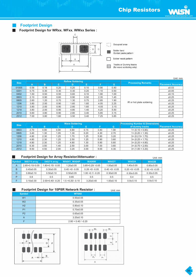
Footprint Design for 10P8R Network Resistor : Unit: mm
Symbol WT04X
W1 0.50±0.05
W2 0.35±0.05
H2 0.80±0.10
P1 0.70±0.05
P2 0.65±0.05
A 3.20±0.10
F 2.80 + 0.40 / -0.20
Footprint Design
Footprint Design for WRxx, WFxx, WWxx Series :
Unit: mm
Reflow SolderingSize
A B C D E F GProcessing Remarks
Placement Accuracy
01005 0.58 0.18 0.20 0.20 0.10 0.90 0.40 ±0.03
0201 0.75 0.30 0.30 0.30 0.20 1.10 0.50 ±0.05
0402 1.50 0.50 0.50 0.60 0.10 1.90 1.00 ±0.15
0603 2.10 0.90 0.60 0.90 0.50 2.35 1.45 ±0.25
0805 2.60 1.20 0.70 1.30 0.75 2.85 1.90 ±0.25
1206 3.80 2.00 0.90 1.60 1.60 4.05 2.25 ±0.25
1210 3.80 2.00 0.90 2.80 1.60 4.05 3.15 ±0.25
1.40 4.20 5.50 ±0.25
3.40 5.85 3.15 ±0.25
2512 7.00 3.80 1.60 3.50 3.40 7.25 3.85
IR or hot plate soldering
±0.25
Wave SolderingSize
A B C D E F G
Processing Number & Dimensions
of dummy tracks Placement Accuracy
0603 2.70 0.90 0.90 0.80 0.15 3.40 1.90 1× (0.15 × 0.80) ±0.25
0805 3.40 1.30 1.05 1.30 0.20 4.30 2.70 1× (0.20 × 1.30) ±0.25
1206 4.80 2.30 1.25 1.70 1.25 5.90 3.20 3× (0.2 5× 1.70) ±0.25
1210 4.80 2.30 1.25 2.50 1.25 5.90 3.60 3× (0.25 × 1.70) ±0.25
1218 4.80 2.30 1.25 4.80 1.30 5.90 5.60 3× (0.25 × 4.80) ±0.25
2010 6.30 3.50 1.40 2.50 3.00 7.00 3.60 3× (0.75 × 2.50) ±0.25
2512 8.50 4.50 2.00 3.20 3.00 9.00 4.30 3× (1.00 × 3.20) ±0.25
1218 3.80 2.00 0.90 4.80
2010 5.60 3.80 0.90 2.80
WA02A WA02B
1.40±0.05 0.80±0.05
0.20 +0/ -0.05 0.30 +0/ -0.05
0.30±0.05 0.30±0.05
0.4 0.5
0.9±0.10 0.9±0.10

21
Chip Resistorswww.passivecomponent.com
Storage and Handling Conditions: 1. Products are recommended to be used up within one year. Check solders ability in case shelf life extension is needed. 2. To store products with following condition:
Temperature :5 to 40Humidity : 20 to 70% relative humidity
3. Caution: a. Don't store products in a corrosive environment such as sulfide, chloride gas, or acid. It may cause oxidization of electrode,
which easily be resulted in poor soldering b. To store products on the shelf and avoid exposure to moisture. c. Don't expose products to excessive shock, vibration, direct sunlight and so on
Precaution of Soldering 1. It is recommended to use a mildly activated rosin flux ( less than 0.1% wt chlorine ) 2. Excessive flux must be avoided 3. When water-soluble flux is used, enough washing is necessary 4. Two times limitations for reflow soldering is highly recommended 5. Solder repair by soldering iron
a. Max. 350 for below 3 seconds is highly recommended b. Do not directly contact termination to avoid thermal shock.
6. Prevent any external force on the products until solder is cooled
Mounting 1. Imperfect adjustment of mounting machine may cause the cracks, the chipping and the alignment error. Check and inspect the
mounting machine in advance. 2. Set the backup pins in proper layout otherwise the components mounted on the backside of the board are damaged. Do not set
these pins at the position of the nozzle. 3. Adjust the bottom dead point of dispenser away from the board when you apply adhesive. 4. Confirm that the products are corresponding to flow soldering when you perform it. 5. Pay attention to the amount of solder because improper amount of solder place large stress on the products and cause cracks
or malfunctions.
Recommendation of Soldering Profiles: In general application, the lead free (Pb-free) termination CRs are used and may be mounted on PCB by IR reflow or wave soldering process with lead-free solder material. The recommended soldering profiles are shown as Fig.1 & 2. The lead-free termination CRs are also suitable on SMT process against lead-containing solder paste. But the soldering temperature should be higher than the melting point of solder paste 30 at least. If the optimized solder joint is requested, increasing soldering time, temperature and concentration of N2 within oven are recommended. Advised IR reflow soldering profile is shown as Fig.3.
3-5 sec

22
www.passivecomponent.com
PLAN & MEMO

23
www.passivecomponent.com PLAN & MEMO