676 IEEE JOURNAL OF SOLID-STATE CIRCUITS, VOL. 47, NO. 3 ...
10
676 IEEE JOURNAL OF SOLID-STATE CIRCUITS, VOL. 47, NO. 3, MARCH 2012 A Low-Power Magnitude Detector for Analysis of Transient-Rich Signals Brandon Rumberg, Student Member, IEEE, and David W. Graham, Member, IEEE Abstract—Magnitude detection, such as envelope detection or RMS estimation, is needed for many low-power signal-analysis applications. In such applications, the temporal accuracy of the magnitude detector is as important as its amplitude accuracy. We present a low-power audio-frequency magnitude detector that simultaneously achieves both high temporal accuracy and high amplitude accuracy. This performance is achieved by rectifying the signal with a high-ripple peak detector and then averaging this rectified signal with an adaptive-time-constant filter. The time constant of this filter decreases with increasing amplitude, enabling the filter to quickly respond on a short time scale to transients, while steady-state ripple is averaged on a longer time scale. The circuit has been fabricated in a 0.18 m CMOS process and consumes only 1.1 nW–1.08 W when tuned for operation from 20 Hz–20 kHz. It exhibits a dynamic range of 70 dB across typical speech frequencies. Index Terms—Analog processing circuits, CMOS integrated circuits, continuous-time circuits, envelope detectors, magnitude detectors, nonlinear dynamic circuits, peak detectors, ultra-low power. I. INTRODUCTION M AGNITUDE-DETECTION circuits—such as en- velope detectors, peak detectors, and RMS-to-DC converters—produce an estimate of a signal’s magnitude and are thus important elements in communications transceivers [1], automatic gain control systems [2], and analog spectral analyzers [3]–[7]. Since the magnitude is a time-varying quan- tity, the accuracy of a magnitude detector has two components: amplitude accuracy and temporal accuracy. Traditionally, the design emphasis of magnitude circuits has been on amplitude accuracy; however, temporal accuracy is crucial when the magnitude changes quickly relative to the frequencies of the underlying carrier signal, such as in speech signals [8]. Thus, temporal accuracy is important in audio-processing systems, including ultra-low-power (ULP) applications such as bionic ears [7], [9] and event detectors for wakeup applications [10]. Existing digital signal processing techniques for temporal accuracy use non-physical, non-causal filters that require pow- erful processing and non-stop data conversion, thereby limiting Manuscript received August 22, 2011; revised November 23, 2011; accepted November 28, 2011. Date of publication January 18, 2012; date of current ver- sion February 23, 2012. This paper was approved by Associate Editor Boris Murmann. This work was supported in part by GTronix, Inc. The authors are with the Lane Department of Computer Science and Electrical Engineering, West Virginia University, Morgantown, WV 26506 USA (e-mail: [email protected]; [email protected]). Color versions of one or more of the figures in this paper are available online at http://ieeexplore.ieee.org. Digital Object Identifier 10.1109/JSSC.2011.2179452 Fig. 1. (a) Schematic of our magnitude detector. (b) Block diagram of an analog spectral-analysis system. their use in ULP systems. Discrete-time analog circuits have also been explored to achieve good temporal accuracy [11]; however, the power level and the sampled-data representation are inappropriate for many ULP signal-analysis systems. In this paper, we present an ULP continuous-time magnitude detector that has been designed with an emphasis on temporal accuracy, while still achieving high amplitude accuracy. Fig. 1(a) shows our magnitude detector, wherein a rectifying nonlinearity provides an initial estimate of the signal’s magni- tude and then a low-pass filter averages this estimate to obtain the final smooth magnitude estimate. For the rectifying non- linearity, we have developed a voltage-mode asymmetric inte- grator. This circuit’s asymmetry causes the average level of its output to shift in proportion to the input magnitude, thereby pro- viding a magnitude estimate that is superimposed with a ripple. This ripple is then smoothed by a nonlinear low-pass filter with an adaptive time constant. We have designed this filter’s non- linearity such that its time constant shrinks in response to large input-output differential signals, thereby reducing the integra- tion window in order to follow transients more closely, while maintaining a long time constant for small signals in order to retain good ripple suppression. 0018-9200/$31.00 © 2012 IEEE
Transcript of 676 IEEE JOURNAL OF SOLID-STATE CIRCUITS, VOL. 47, NO. 3 ...
676 IEEE JOURNAL OF SOLID-STATE CIRCUITS, VOL. 47, NO. 3, MARCH 2012
A Low-Power Magnitude Detector for Analysis ofTransient-Rich Signals
Brandon Rumberg, Student Member, IEEE, and David W. Graham, Member, IEEE
Abstract—Magnitude detection, such as envelope detection orRMS estimation, is needed for many low-power signal-analysisapplications. In such applications, the temporal accuracy of themagnitude detector is as important as its amplitude accuracy. Wepresent a low-power audio-frequency magnitude detector thatsimultaneously achieves both high temporal accuracy and highamplitude accuracy. This performance is achieved by rectifyingthe signal with a high-ripple peak detector and then averagingthis rectified signal with an adaptive-time-constant filter. Thetime constant of this filter decreases with increasing amplitude,enabling the filter to quickly respond on a short time scale totransients, while steady-state ripple is averaged on a longer timescale. The circuit has been fabricated in a 0.18 m CMOS processand consumes only 1.1 nW–1.08 W when tuned for operationfrom 20 Hz–20 kHz. It exhibits a dynamic range of 70 dB acrosstypical speech frequencies.
Index Terms—Analog processing circuits, CMOS integratedcircuits, continuous-time circuits, envelope detectors, magnitudedetectors, nonlinear dynamic circuits, peak detectors, ultra-lowpower.
I. INTRODUCTION
M AGNITUDE-DETECTION circuits—such as en-velope detectors, peak detectors, and RMS-to-DC
converters—produce an estimate of a signal’s magnitude andare thus important elements in communications transceivers[1], automatic gain control systems [2], and analog spectralanalyzers [3]–[7]. Since the magnitude is a time-varying quan-tity, the accuracy of a magnitude detector has two components:amplitude accuracy and temporal accuracy. Traditionally, thedesign emphasis of magnitude circuits has been on amplitudeaccuracy; however, temporal accuracy is crucial when themagnitude changes quickly relative to the frequencies of theunderlying carrier signal, such as in speech signals [8]. Thus,temporal accuracy is important in audio-processing systems,including ultra-low-power (ULP) applications such as bionicears [7], [9] and event detectors for wakeup applications [10].Existing digital signal processing techniques for temporalaccuracy use non-physical, non-causal filters that require pow-erful processing and non-stop data conversion, thereby limiting
Manuscript received August 22, 2011; revised November 23, 2011; acceptedNovember 28, 2011. Date of publication January 18, 2012; date of current ver-sion February 23, 2012. This paper was approved by Associate Editor BorisMurmann. This work was supported in part by GTronix, Inc.The authors arewith the LaneDepartment of Computer Science and Electrical
Engineering, West Virginia University, Morgantown, WV 26506 USA (e-mail:[email protected]; [email protected]).Color versions of one or more of the figures in this paper are available online
at http://ieeexplore.ieee.org.Digital Object Identifier 10.1109/JSSC.2011.2179452
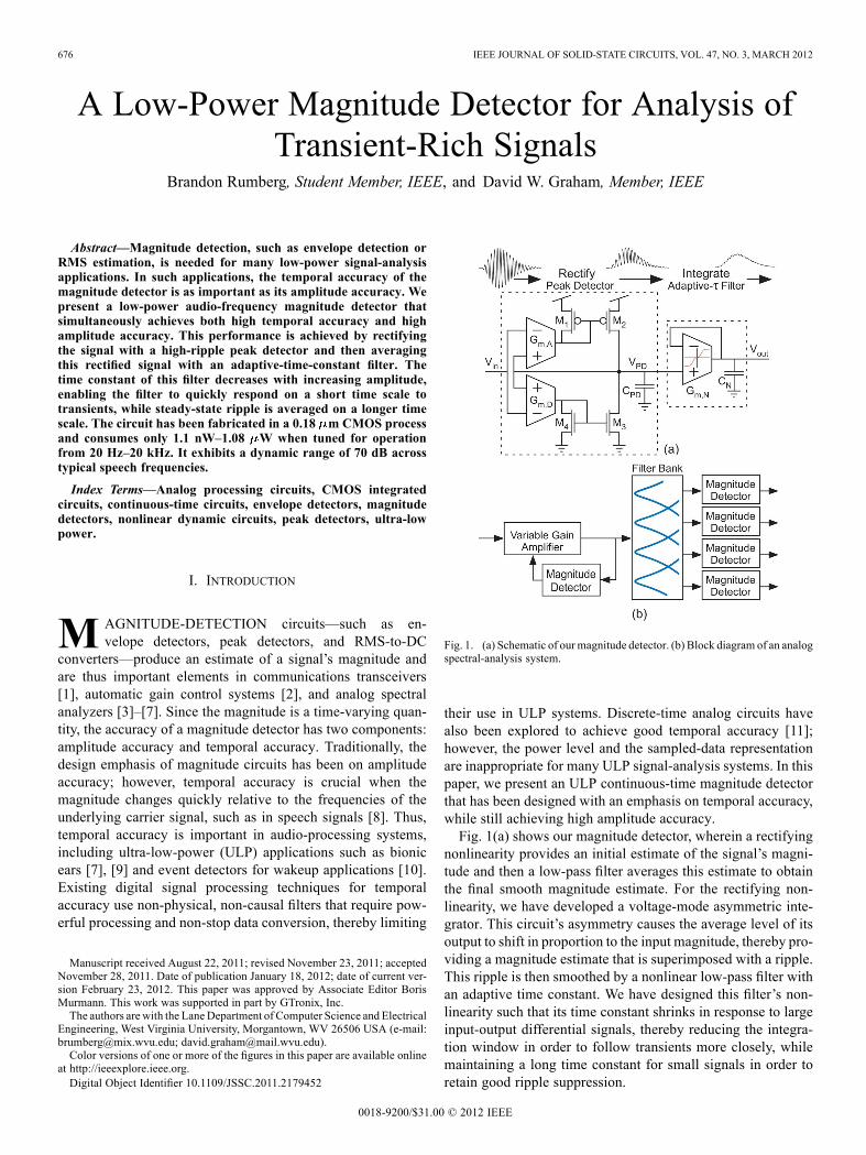
Fig. 1. (a) Schematic of ourmagnitude detector. (b) Block diagram of an analogspectral-analysis system.
their use in ULP systems. Discrete-time analog circuits havealso been explored to achieve good temporal accuracy [11];however, the power level and the sampled-data representationare inappropriate for many ULP signal-analysis systems. In thispaper, we present an ULP continuous-time magnitude detectorthat has been designed with an emphasis on temporal accuracy,while still achieving high amplitude accuracy.Fig. 1(a) shows our magnitude detector, wherein a rectifying
nonlinearity provides an initial estimate of the signal’s magni-tude and then a low-pass filter averages this estimate to obtainthe final smooth magnitude estimate. For the rectifying non-linearity, we have developed a voltage-mode asymmetric inte-grator. This circuit’s asymmetry causes the average level of itsoutput to shift in proportion to the input magnitude, thereby pro-viding a magnitude estimate that is superimposed with a ripple.This ripple is then smoothed by a nonlinear low-pass filter withan adaptive time constant. We have designed this filter’s non-linearity such that its time constant shrinks in response to largeinput-output differential signals, thereby reducing the integra-tion window in order to follow transients more closely, whilemaintaining a long time constant for small signals in order toretain good ripple suppression.
0018-9200/$31.00 © 2012 IEEE
RUMBERG AND GRAHAM: A LOW-POWER MAGNITUDE DETECTOR FOR ANALYSIS OF TRANSIENT-RICH SIGNALS 677
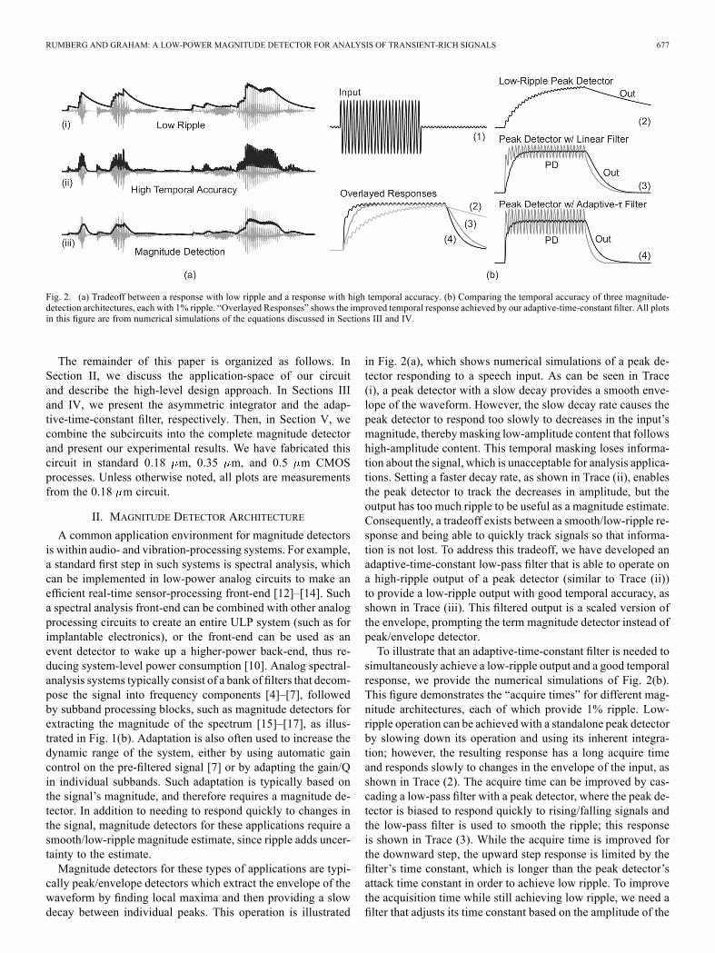
Fig. 2. (a) Tradeoff between a response with low ripple and a response with high temporal accuracy. (b) Comparing the temporal accuracy of three magnitude-detection architectures, each with 1% ripple. “Overlayed Responses” shows the improved temporal response achieved by our adaptive-time-constant filter. All plotsin this figure are from numerical simulations of the equations discussed in Sections III and IV.
The remainder of this paper is organized as follows. InSection II, we discuss the application-space of our circuitand describe the high-level design approach. In Sections IIIand IV, we present the asymmetric integrator and the adap-tive-time-constant filter, respectively. Then, in Section V, wecombine the subcircuits into the complete magnitude detectorand present our experimental results. We have fabricated thiscircuit in standard 0.18 m, 0.35 m, and 0.5 m CMOSprocesses. Unless otherwise noted, all plots are measurementsfrom the 0.18 m circuit.
II. MAGNITUDE DETECTOR ARCHITECTURE
A common application environment for magnitude detectorsis within audio- and vibration-processing systems. For example,a standard first step in such systems is spectral analysis, whichcan be implemented in low-power analog circuits to make anefficient real-time sensor-processing front-end [12]–[14]. Sucha spectral analysis front-end can be combined with other analogprocessing circuits to create an entire ULP system (such as forimplantable electronics), or the front-end can be used as anevent detector to wake up a higher-power back-end, thus re-ducing system-level power consumption [10]. Analog spectral-analysis systems typically consist of a bank of filters that decom-pose the signal into frequency components [4]–[7], followedby subband processing blocks, such as magnitude detectors forextracting the magnitude of the spectrum [15]–[17], as illus-trated in Fig. 1(b). Adaptation is also often used to increase thedynamic range of the system, either by using automatic gaincontrol on the pre-filtered signal [7] or by adapting the gain/Qin individual subbands. Such adaptation is typically based onthe signal’s magnitude, and therefore requires a magnitude de-tector. In addition to needing to respond quickly to changes inthe signal, magnitude detectors for these applications require asmooth/low-ripple magnitude estimate, since ripple adds uncer-tainty to the estimate.Magnitude detectors for these types of applications are typi-
cally peak/envelope detectors which extract the envelope of thewaveform by finding local maxima and then providing a slowdecay between individual peaks. This operation is illustrated
in Fig. 2(a), which shows numerical simulations of a peak de-tector responding to a speech input. As can be seen in Trace(i), a peak detector with a slow decay provides a smooth enve-lope of the waveform. However, the slow decay rate causes thepeak detector to respond too slowly to decreases in the input’smagnitude, therebymasking low-amplitude content that followshigh-amplitude content. This temporal masking loses informa-tion about the signal, which is unacceptable for analysis applica-tions. Setting a faster decay rate, as shown in Trace (ii), enablesthe peak detector to track the decreases in amplitude, but theoutput has too much ripple to be useful as a magnitude estimate.Consequently, a tradeoff exists between a smooth/low-ripple re-sponse and being able to quickly track signals so that informa-tion is not lost. To address this tradeoff, we have developed anadaptive-time-constant low-pass filter that is able to operate ona high-ripple output of a peak detector (similar to Trace (ii))to provide a low-ripple output with good temporal accuracy, asshown in Trace (iii). This filtered output is a scaled version ofthe envelope, prompting the term magnitude detector instead ofpeak/envelope detector.To illustrate that an adaptive-time-constant filter is needed to
simultaneously achieve a low-ripple output and a good temporalresponse, we provide the numerical simulations of Fig. 2(b).This figure demonstrates the “acquire times” for different mag-nitude architectures, each of which provide 1% ripple. Low-ripple operation can be achieved with a standalone peak detectorby slowing down its operation and using its inherent integra-tion; however, the resulting response has a long acquire timeand responds slowly to changes in the envelope of the input, asshown in Trace (2). The acquire time can be improved by cas-cading a low-pass filter with a peak detector, where the peak de-tector is biased to respond quickly to rising/falling signals andthe low-pass filter is used to smooth the ripple; this responseis shown in Trace (3). While the acquire time is improved forthe downward step, the upward step response is limited by thefilter’s time constant, which is longer than the peak detector’sattack time constant in order to achieve low ripple. To improvethe acquisition time while still achieving low ripple, we need afilter that adjusts its time constant based on the amplitude of the
678 IEEE JOURNAL OF SOLID-STATE CIRCUITS, VOL. 47, NO. 3, MARCH 2012
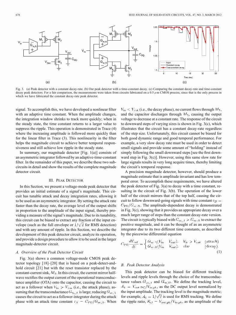
Fig. 3. (a) Peak detector with a constant decay-rate. (b) Our peak detector with a time-constant decay. (c) Comparing the constant decay-rate and time-constantdecay peak detectors. For a fair comparison, the measurements were taken from circuits fabricated on a 0.5 m CMOS process, since that is the only process inwhich we have fabricated the constant decay-rate peak detector.
signal. To accomplish this, we have developed a nonlinear filterwith an adaptive time constant. When the amplitude changes,the integration window shrinks to track more quickly; when inthe steady state, the time constant returns to a larger value tosuppress the ripple. This operation is demonstrated in Trace (4)where the increasing amplitude is followed more quickly thanfor the linear filter in Trace (3). This nonlinearity in the filterhelps the magnitude circuit to achieve better temporal respon-siveness and still achieve low ripple in the steady state.In summary, our magnitude detector [Fig. 1(a)] consists of
an asymmetric integrator followed by an adaptive-time-constantfilter. In the remainder of this paper, we describe these two sub-circuits in detail and show the results of the complete magnitudedetector circuit.
III. PEAK DETECTOR
In this Section, we present a voltage-mode peak detector thatprovides an initial estimate of a signal’s magnitude. This cir-cuit has tunable attack and decay integration rates, allowing itto be used as an asymmetric integrator. By setting the attack ratefaster than the decay rate, the average level of the output shiftsin proportion to the amplitude of the input signal, thereby pro-viding a measure of the signal’s magnitude. Due to its tunability,this circuit can be biased to extract any fraction of the input en-velope (such as the full envelope or for RMS detection)and with any amount of ripple. In this Section, we describe thedevelopment of this peak detector circuit, analyze its operation,and provide a design procedure to allow it to be used in the largermagnitude-detector circuit.
A. Overview of the Peak Detector Circuit
Fig. 3(a) shows a common voltage-mode CMOS peak de-tector topology [18]–[20] that is based on a peak-detect-and-hold circuit [21] but with the reset transistor replaced by theconstant-current sink, . In this circuit, the currentmirror half-wave rectifies the output current of the operational transconduc-tance amplifier (OTA) onto the capacitor, causing the circuit toact as a follower when (i.e., the attack phase), as-suming that the transconductance is large; reducingcauses the circuit to act as a follower-integrator during the attackphase with an attack time constant . When
(i.e., the decay phase), no current flows through ,and the capacitor discharges through , causing the outputvoltage to decrease at a constant rate. The response of the circuitto downward steps of varying sizes is shown in Fig. 3(c), whichillustrates that the circuit has a constant decay-rate regardlessof the step size. Unfortunately, this circuit cannot be biased forboth good dynamic range and good temporal performance. Forexample, a very slow decay rate must be used in order to detectsmall signals and provide some amount of “holding” instead ofsimply following the small downward steps [see the first down-ward step in Fig. 3(c)]. However, using this same slow rate forlarge signals results in very long acquire times, thereby limitingthe circuit’s temporal response.A precision magnitude detector, however, should produce a
magnitude estimate that is amplitude invariant and has low tem-poral error. To accomplish these requirements, we have alteredthe peak detector of Fig. 3(a) to decay with a time constant, re-sulting in the circuit of Fig. 3(b). The operation of the lowerhalf of the circuit mirrors that of the top half, causing the cir-cuit to follow downward-going signals with time constant
. The amplitude-dependent decay is demonstratedin Fig. 3(c), showing that it provides an appropriate decay over amuch larger range of steps than the constant decay-rate version.The circuit is typically biased with to extract thepositive magnitude, and it can be thought of as an asymmetricintegrator due to its two different time constants, as describedby the piecewise differential equation
(1)
B. Peak Detector Analysis
This peak detector can be biased for different trackinglevels and ripple levels through the choice of the transconduc-tance values and . We define the tracking level,
, as the DC output level normalized bythe input amplitude. The tracking level is the magnitude metric;for example, is used for RMS tracking. We definethe ripple ratio, , as the amplitude of the
RUMBERG AND GRAHAM: A LOW-POWER MAGNITUDE DETECTOR FOR ANALYSIS OF TRANSIENT-RICH SIGNALS 679
output ripple normalized by the amplitude of the input. Typi-cally, the peak detector is tuned for 10%–30% ripple to achieve1% ripple from the complete magnitude circuit, as discussedfurther in Section V. To design and bias this peak detector foruse in the complete magnitude detector, we need to know howto choose the biases to achieve the specified tracking levels andripple amounts.To derive the dependence of both the tracking level and
the ripple ratio upon the peak detector’s biases, we haveused the harmonic balance method [22], [23]. This procedureuses (1) modeled in the form of Fig. 4(a), and it assumesa sinusoidal input. First, the output equation is written interms of both the tracking level and the output ripple, yielding
, where is theinput amplitude and is the phase shift from the input to theoutput. Next, this equation is applied to (1), and the termsare balanced both at 0 Hz and at the fundamental frequencyto obtain equations for the tracking level and the ripple ratio,respectively. Since the peak detector has a low-pass form, wehave neglected the harmonics of the fundamental to derivean approximation that is sufficient for choosing biases andpredicting the operation of the circuit.By solving the loop at 0 Hz, the following equations were
obtained for the tracking level, :
(2)
(3)
is the amplitude at node normalized by the input am-plitude. As shown by (2), the tracking level depends on theratio of transconductances and also on the output ripple; thiswas verified experimentally in Fig. 4(b), which shows how thetracking level varies with the attack-to-decay ratio for a fixedoutput ripple ratio . As expected, the tracking levelis zero/centered when , and the tracking levelincreases as is increased above , saturating as thetracking level approaches 100%.By solving the loop at the fundamental frequency, , the fol-
lowing equation was obtained for the output ripple, :
(4)
where . In normal operation, the peak de-tector is tuned for a particular operating frequency by using thetransconductances to obtain the desired ripple at that frequency.This procedure is demonstrated in Fig. 4(c), wherein (2) and (4)are used to bias the circuit for (10% ripple) at threedifferent frequencies: 500 Hz, 5 kHz, and 50 kHz. The ripple hasa first-order low-pass dependence on frequency, since the circuitis a first-order asymmetric integrator. The ripple increases asthe frequency decreases, until the frequency is below the corner
Fig. 4. (a) Model that is used for analyzing the peak detector. (b) Peak detectortracking level as a function of the attack-to-decay ratio. (c) Ripple as a functionof frequency for three different biases: targeting 10% ripple at 500 Hz, 5 kHz,and 50 kHz. The data in (b) and (c) were measured with a peak detector fabri-cated on a 0.35 m CMOS process, since we did not have direct access to thepeak detector output with the 0.18 m circuit.
frequency of the peak detector, at which point the peak detectoracts as a follower. In order to maintain peak detector operation,the signal frequency must remain within the 20 dB/decadeslope region; if the signal frequency drops too low, then the cir-cuit no longer performs rectification. Thus, if the circuit is goingto be used for broadband operation, it should be biased such thatthe lowest frequencies of interest remain above the corner fre-quency. For example, in the broadband speech demonstration ofFig. 11, the peak detector was biased for 30% ripple at 200 Hz,which is within the range of fundamental frequencies for speech[8]. If the circuit is used for subband operation, such as the filter
680 IEEE JOURNAL OF SOLID-STATE CIRCUITS, VOL. 47, NO. 3, MARCH 2012
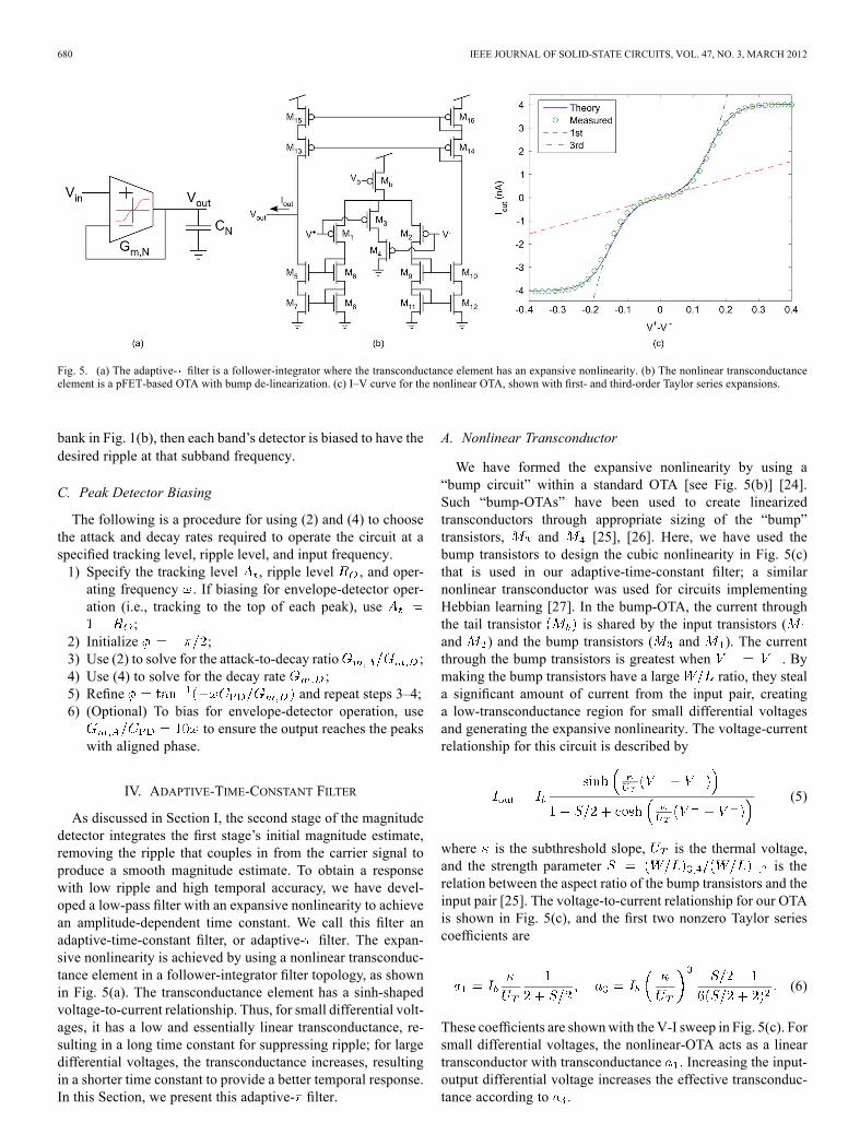
Fig. 5. (a) The adaptive- filter is a follower-integrator where the transconductance element has an expansive nonlinearity. (b) The nonlinear transconductanceelement is a pFET-based OTA with bump de-linearization. (c) I–V curve for the nonlinear OTA, shown with first- and third-order Taylor series expansions.
bank in Fig. 1(b), then each band’s detector is biased to have thedesired ripple at that subband frequency.
C. Peak Detector Biasing
The following is a procedure for using (2) and (4) to choosethe attack and decay rates required to operate the circuit at aspecified tracking level, ripple level, and input frequency.1) Specify the tracking level , ripple level , and oper-ating frequency . If biasing for envelope-detector oper-ation (i.e., tracking to the top of each peak), use
;2) Initialize ;3) Use (2) to solve for the attack-to-decay ratio ;4) Use (4) to solve for the decay rate ;5) Refine and repeat steps 3–4;6) (Optional) To bias for envelope-detector operation, use
to ensure the output reaches the peakswith aligned phase.
IV. ADAPTIVE-TIME-CONSTANT FILTER
As discussed in Section I, the second stage of the magnitudedetector integrates the first stage’s initial magnitude estimate,removing the ripple that couples in from the carrier signal toproduce a smooth magnitude estimate. To obtain a responsewith low ripple and high temporal accuracy, we have devel-oped a low-pass filter with an expansive nonlinearity to achievean amplitude-dependent time constant. We call this filter anadaptive-time-constant filter, or adaptive- filter. The expan-sive nonlinearity is achieved by using a nonlinear transconduc-tance element in a follower-integrator filter topology, as shownin Fig. 5(a). The transconductance element has a sinh-shapedvoltage-to-current relationship. Thus, for small differential volt-ages, it has a low and essentially linear transconductance, re-sulting in a long time constant for suppressing ripple; for largedifferential voltages, the transconductance increases, resultingin a shorter time constant to provide a better temporal response.In this Section, we present this adaptive- filter.
A. Nonlinear Transconductor
We have formed the expansive nonlinearity by using a“bump circuit” within a standard OTA [see Fig. 5(b)] [24].Such “bump-OTAs” have been used to create linearizedtransconductors through appropriate sizing of the “bump”transistors, and [25], [26]. Here, we have used thebump transistors to design the cubic nonlinearity in Fig. 5(c)that is used in our adaptive-time-constant filter; a similarnonlinear transconductor was used for circuits implementingHebbian learning [27]. In the bump-OTA, the current throughthe tail transistor is shared by the input transistors (and ) and the bump transistors ( and ). The currentthrough the bump transistors is greatest when . Bymaking the bump transistors have a large ratio, they steala significant amount of current from the input pair, creatinga low-transconductance region for small differential voltagesand generating the expansive nonlinearity. The voltage-currentrelationship for this circuit is described by
(5)
where is the subthreshold slope, is the thermal voltage,and the strength parameter is therelation between the aspect ratio of the bump transistors and theinput pair [25]. The voltage-to-current relationship for our OTAis shown in Fig. 5(c), and the first two nonzero Taylor seriescoefficients are
(6)
These coefficients are shownwith the V-I sweep in Fig. 5(c). Forsmall differential voltages, the nonlinear-OTA acts as a lineartransconductor with transconductance . Increasing the input-output differential voltage increases the effective transconduc-tance according to .
RUMBERG AND GRAHAM: A LOW-POWER MAGNITUDE DETECTOR FOR ANALYSIS OF TRANSIENT-RICH SIGNALS 681
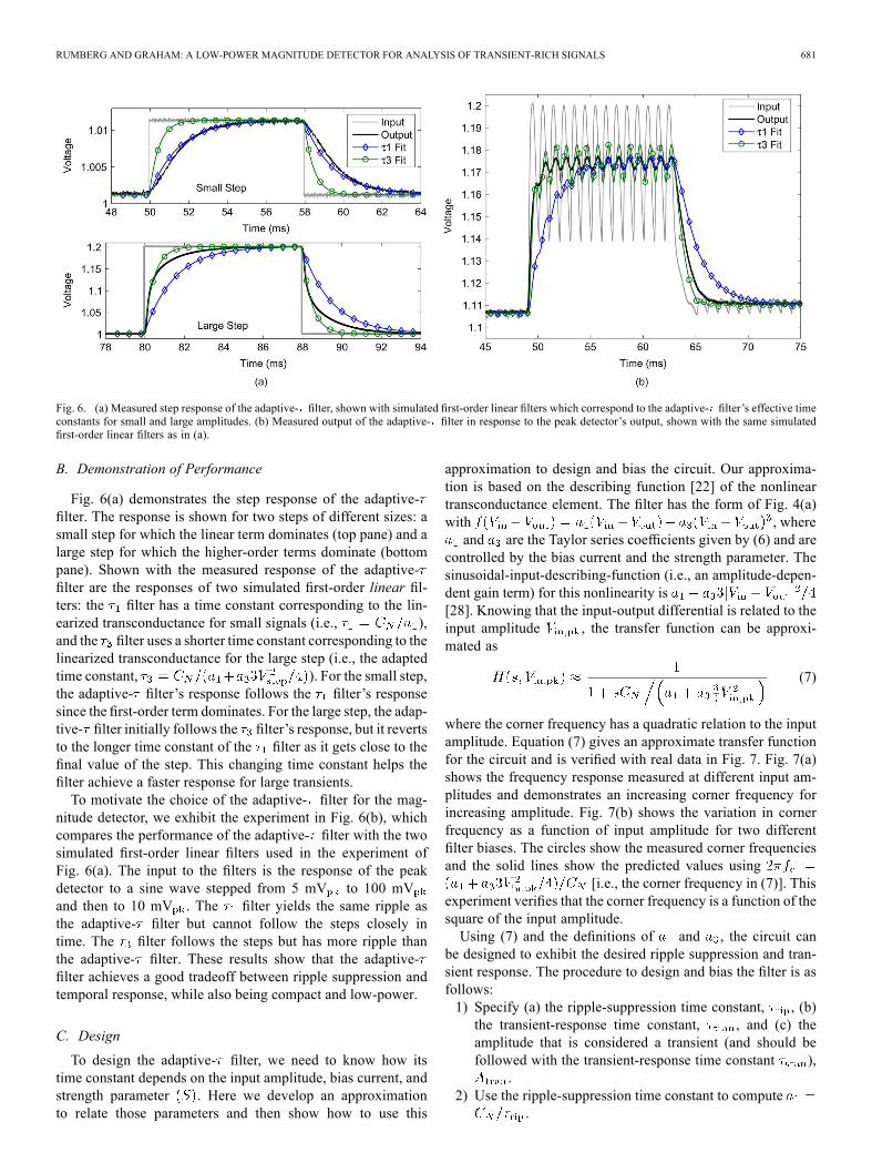
Fig. 6. (a) Measured step response of the adaptive- filter, shown with simulated first-order linear filters which correspond to the adaptive- filter’s effective timeconstants for small and large amplitudes. (b) Measured output of the adaptive- filter in response to the peak detector’s output, shown with the same simulatedfirst-order linear filters as in (a).
B. Demonstration of Performance
Fig. 6(a) demonstrates the step response of the adaptive-filter. The response is shown for two steps of different sizes: asmall step for which the linear term dominates (top pane) and alarge step for which the higher-order terms dominate (bottompane). Shown with the measured response of the adaptive-filter are the responses of two simulated first-order linear fil-ters: the filter has a time constant corresponding to the lin-earized transconductance for small signals (i.e., ),and the filter uses a shorter time constant corresponding to thelinearized transconductance for the large step (i.e., the adaptedtime constant, ). For the small step,the adaptive- filter’s response follows the filter’s responsesince the first-order term dominates. For the large step, the adap-tive- filter initially follows the filter’s response, but it revertsto the longer time constant of the filter as it gets close to thefinal value of the step. This changing time constant helps thefilter achieve a faster response for large transients.To motivate the choice of the adaptive- filter for the mag-
nitude detector, we exhibit the experiment in Fig. 6(b), whichcompares the performance of the adaptive- filter with the twosimulated first-order linear filters used in the experiment ofFig. 6(a). The input to the filters is the response of the peakdetector to a sine wave stepped from 5 mV to 100 mVand then to 10 mV . The filter yields the same ripple asthe adaptive- filter but cannot follow the steps closely intime. The filter follows the steps but has more ripple thanthe adaptive- filter. These results show that the adaptive-filter achieves a good tradeoff between ripple suppression andtemporal response, while also being compact and low-power.
C. Design
To design the adaptive- filter, we need to know how itstime constant depends on the input amplitude, bias current, andstrength parameter . Here we develop an approximationto relate those parameters and then show how to use this
approximation to design and bias the circuit. Our approxima-tion is based on the describing function [22] of the nonlineartransconductance element. The filter has the form of Fig. 4(a)with , whereand are the Taylor series coefficients given by (6) and are
controlled by the bias current and the strength parameter. Thesinusoidal-input-describing-function (i.e., an amplitude-depen-dent gain term) for this nonlinearity is[28]. Knowing that the input-output differential is related to theinput amplitude , the transfer function can be approxi-mated as
(7)
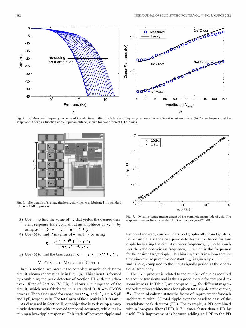
where the corner frequency has a quadratic relation to the inputamplitude. Equation (7) gives an approximate transfer functionfor the circuit and is verified with real data in Fig. 7. Fig. 7(a)shows the frequency response measured at different input am-plitudes and demonstrates an increasing corner frequency forincreasing amplitude. Fig. 7(b) shows the variation in cornerfrequency as a function of input amplitude for two differentfilter biases. The circles show the measured corner frequenciesand the solid lines show the predicted values using
[i.e., the corner frequency in (7)]. Thisexperiment verifies that the corner frequency is a function of thesquare of the input amplitude.Using (7) and the definitions of and , the circuit can
be designed to exhibit the desired ripple suppression and tran-sient response. The procedure to design and bias the filter is asfollows:1) Specify (a) the ripple-suppression time constant, , (b)the transient-response time constant, , and (c) theamplitude that is considered a transient (and should befollowed with the transient-response time constant ),
.2) Use the ripple-suppression time constant to compute
.
682 IEEE JOURNAL OF SOLID-STATE CIRCUITS, VOL. 47, NO. 3, MARCH 2012
Fig. 7. (a) Measured frequency response of the adaptive- filter. Each line is a frequency response for a different input amplitude. (b) Corner frequency of theadaptive- filter as a function of the input amplitude, shown for two different OTA biases.
Fig. 8. Micrograph of the magnitude circuit, which was fabricated in a standard0.18 m CMOS process.
3) Use to find the value of that yields the desired tran-sient-response time constant at an amplitude of byusing .
4) Use (6) to find in terms of and by using
5) Use (6) to find the bias current .
V. COMPLETE MAGNITUDE CIRCUIT
In this section, we present the complete magnitude detectorcircuit, shown schematically in Fig. 1(a). This circuit is formedby combining the peak detector of Section III with the adap-tive- filter of Section IV. Fig. 8 shows a micrograph of thecircuit, which was fabricated in a standard 0.18 m CMOSprocess. The values used for capacitors and are 4.5 pFand 3 pF, respectively. The total area of the circuit is 0.019 mm .As discussed in Section II, our objective is to develop a mag-
nitude detector with improved temporal accuracy, while main-taining a low-ripple response. This tradeoff between ripple and
Fig. 9. Dynamic range measurement of the complete magnitude circuit. Theresponse remains linear to within 1 dB across a range of 70 dB.
temporal accuracy can be understood graphically from Fig. 4(c).For example, a standalone peak detector can be tuned for lowripple by biasing the circuit’s corner frequency, , to be muchless than the operational frequency, , which is the frequencyfor the desired target ripple. This biasing results in a long acquiretime since the acquire time constant, , is given byand is long compared to the input signal’s period at the opera-tional frequency.The product is related to the number of cycles required
to acquire transients and is thus a good metric for temporal re-sponsiveness. In Table I, we compare for different magni-tude-detection architectures for a given total ripple at the output,. The third column states the factor of improvement for each
architecture with 1% total ripple over the baseline case of thestandalone peak detector (PD). For example, a PD combinedwith a low-pass filter (LPF) is 7.1 times faster than a PD byitself. This improvement is because adding an LPF to the PD

RUMBERG AND GRAHAM: A LOW-POWER MAGNITUDE DETECTOR FOR ANALYSIS OF TRANSIENT-RICH SIGNALS 683
Fig. 10. Measured transient response of the magnitude detector for logarithmically increasing amplitude from 2 mV to 500 mV .
Fig. 11. Measured response of the magnitude circuit to a speech waveform. For comparison, the response is shown with a computer calculated RMS.
TABLE ITRADEOFF BETWEEN RIPPLE AND ACQUISITION TIME
increases the slope of the ripple-frequency relationship [i.e., theslope of Fig. 4(c)], thereby moving closer to ; the best resultis obtained by splitting the ripple suppression evenly betweenthe PD and the linear LPF (e.g., 10% suppression in each stage
to obtain 1% total suppression). Using a second-order filter fur-ther improves the temporal accuracy by increasing the slope ofthe ripple-frequency relationship. However, this technique onlyachieves 1.6-times improvement beyond the first-order filter,while adding significant increases in power, area, and frequencysensitivity (due to the larger slope). With the adaptive- filter,we operate the peak detector faster than with the linear filter(typically twice as fast) which, accordingly, yields more rippleat the PD’s output. To achieve the same total ripple at the outputof the magnitude detector, the value of in the adap-tive- filter is tuned to compensate for the increased PD speed.Large transients then cause the filter’s time constant to decreasesuch that the PD’s speed is the main limitation to the magni-tude detector’s overall speed. As can be seen from the table, the
684 IEEE JOURNAL OF SOLID-STATE CIRCUITS, VOL. 47, NO. 3, MARCH 2012
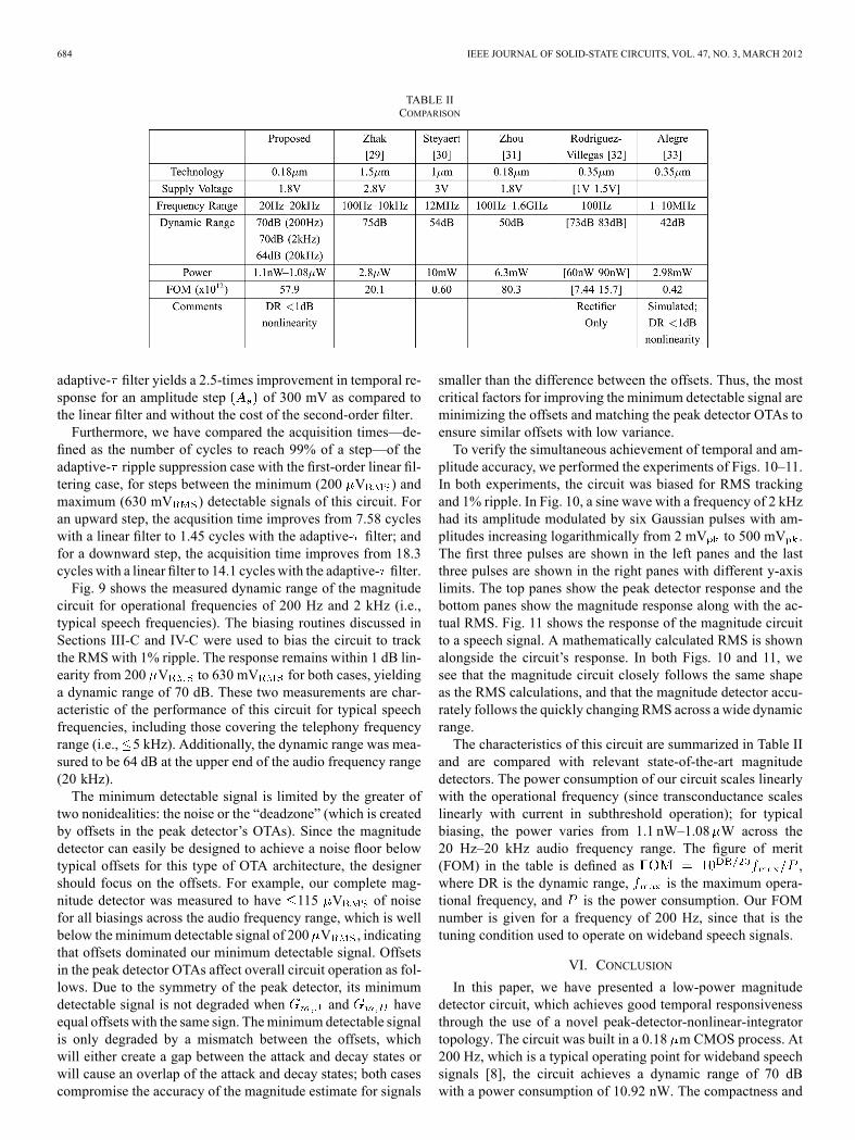
TABLE IICOMPARISON
adaptive- filter yields a 2.5-times improvement in temporal re-sponse for an amplitude step of 300 mV as compared tothe linear filter and without the cost of the second-order filter.Furthermore, we have compared the acquisition times—de-
fined as the number of cycles to reach 99% of a step—of theadaptive- ripple suppression case with the first-order linear fil-tering case, for steps between the minimum (200 V ) andmaximum (630 mV ) detectable signals of this circuit. Foran upward step, the acqusition time improves from 7.58 cycleswith a linear filter to 1.45 cycles with the adaptive- filter; andfor a downward step, the acquisition time improves from 18.3cycles with a linear filter to 14.1 cycles with the adaptive- filter.Fig. 9 shows the measured dynamic range of the magnitude
circuit for operational frequencies of 200 Hz and 2 kHz (i.e.,typical speech frequencies). The biasing routines discussed inSections III-C and IV-C were used to bias the circuit to trackthe RMS with 1% ripple. The response remains within 1 dB lin-earity from 200 V to 630 mV for both cases, yieldinga dynamic range of 70 dB. These two measurements are char-acteristic of the performance of this circuit for typical speechfrequencies, including those covering the telephony frequencyrange (i.e., 5 kHz). Additionally, the dynamic range was mea-sured to be 64 dB at the upper end of the audio frequency range(20 kHz).The minimum detectable signal is limited by the greater of
two nonidealities: the noise or the “deadzone” (which is createdby offsets in the peak detector’s OTAs). Since the magnitudedetector can easily be designed to achieve a noise floor belowtypical offsets for this type of OTA architecture, the designershould focus on the offsets. For example, our complete mag-nitude detector was measured to have 115 V of noisefor all biasings across the audio frequency range, which is wellbelow the minimum detectable signal of 200 V , indicatingthat offsets dominated our minimum detectable signal. Offsetsin the peak detector OTAs affect overall circuit operation as fol-lows. Due to the symmetry of the peak detector, its minimumdetectable signal is not degraded when and haveequal offsets with the same sign. Theminimum detectable signalis only degraded by a mismatch between the offsets, whichwill either create a gap between the attack and decay states orwill cause an overlap of the attack and decay states; both casescompromise the accuracy of the magnitude estimate for signals
smaller than the difference between the offsets. Thus, the mostcritical factors for improving the minimum detectable signal areminimizing the offsets and matching the peak detector OTAs toensure similar offsets with low variance.To verify the simultaneous achievement of temporal and am-
plitude accuracy, we performed the experiments of Figs. 10–11.In both experiments, the circuit was biased for RMS trackingand 1% ripple. In Fig. 10, a sine wave with a frequency of 2 kHzhad its amplitude modulated by six Gaussian pulses with am-plitudes increasing logarithmically from 2 mV to 500 mV .The first three pulses are shown in the left panes and the lastthree pulses are shown in the right panes with different y-axislimits. The top panes show the peak detector response and thebottom panes show the magnitude response along with the ac-tual RMS. Fig. 11 shows the response of the magnitude circuitto a speech signal. A mathematically calculated RMS is shownalongside the circuit’s response. In both Figs. 10 and 11, wesee that the magnitude circuit closely follows the same shapeas the RMS calculations, and that the magnitude detector accu-rately follows the quickly changing RMS across a wide dynamicrange.The characteristics of this circuit are summarized in Table II
and are compared with relevant state-of-the-art magnitudedetectors. The power consumption of our circuit scales linearlywith the operational frequency (since transconductance scaleslinearly with current in subthreshold operation); for typicalbiasing, the power varies from 1.1 nW–1.08 W across the20 Hz–20 kHz audio frequency range. The figure of merit(FOM) in the table is defined as ,where DR is the dynamic range, is the maximum opera-tional frequency, and is the power consumption. Our FOMnumber is given for a frequency of 200 Hz, since that is thetuning condition used to operate on wideband speech signals.
VI. CONCLUSION
In this paper, we have presented a low-power magnitudedetector circuit, which achieves good temporal responsivenessthrough the use of a novel peak-detector-nonlinear-integratortopology. The circuit was built in a 0.18 m CMOS process. At200 Hz, which is a typical operating point for wideband speechsignals [8], the circuit achieves a dynamic range of 70 dBwith a power consumption of 10.92 nW. The compactness and
RUMBERG AND GRAHAM: A LOW-POWER MAGNITUDE DETECTOR FOR ANALYSIS OF TRANSIENT-RICH SIGNALS 685
low-power operation of the circuit, combined with its flexiblebiasing, make it a good choice for applications such as spectralanalysis.
ACKNOWLEDGMENT
The authors would like to thank Paul D. Smith for useful con-versations related to magnitude detection, and GTronix, Inc. forintegrated-circuit fabrication.
REFERENCES[1] F. Yuan, “Design techniques for ASK demodulators of passive wire-
less microsystems: a state-of-the-art review,” Analog Integr. CircuitsSignal Process., vol. 63, pp. 33–45, 2010.
[2] M. Baker and R. Sarpeshkar, “Low-power single-loop and dual-loopAGCs for bionic ears,” IEEE J. Solid-State Circuits, vol. 41, no. 9, pp.1983–1996, Sep. 2006.
[3] D. Graham, P. Smith, R. Chawla, and P. Hasler, “A programmablebandpass array using floating-gate elements,” in Proc. IEEE Int. Symp.Circuits and Systems (ISCAS), Vancouver, BC, Canada, May 2004, vol.1, pp. I-97–I-100.
[4] E. Fragniére, “A 100-channel analog CMOS auditory filter bank forspeech recognition,” in IEEE ISSCC Dig. Tech. Papers, Feb. 2005, vol.1, pp. 140–141.
[5] B. Wen and K. Boahen, “A 360-channel speech preprocessor that em-ulates the cochlear amplifier,” in IEEE ISSCC Dig. Tech. Papers, Feb.2006, pp. 2268–2277.
[6] S.-C. Liu, A. van Schaik, B. Minch, and T. Delbrück, “Event-based64-channel binaural silicon cochlea with Q enhancement mecha-nisms,” in Proc. IEEE Int. Symp. Circuits and Systems (ISCAS), May2010, pp. 2027–2030.
[7] R. Sarpeshkar, C. Salthouse, J.-J. Sit, M. Baker, S. Zhak, T.-T. Lu, L.Turicchia, and S. Balster, “An ultra-low-power programmable analogbionic ear processor,” IEEE Trans. Biomed. Eng., vol. 52, no. 4, pp.711–727, Apr. 2005.
[8] J. Picone, “Signal modeling techniques in speech recognition,” Proc.IEEE, vol. 81, no. 9, pp. 1215–1247, Sep. 1993.
[9] J. Georgiou and C. Toumazou, “A 126- W cochlear chip for a totallyimplantable system,” IEEE J. Solid-State Circuits, vol. 40, no. 2, pp.430–443, Feb. 2005.
[10] B. Rumberg, D. Graham, V. Kulathumani, and R. Fernandez, “Hiber-nets: Energy-efficient sensor networks using analog signal processing,”IEEE J. Emerging and Selected Topics in Circuits and Systems, vol. 1,no. 3, pp. 321–334, Sep. 2011.
[11] J. Alegre, S. Celma, B. Calvo, and J. G. del Pozo, “A novel CMOSenvelope detector structure,” in Proc. IEEE Int. Symp. Circuits Syst.(ISCAS), 2007, pp. 3538–3541.
[12] P. Hasler, P. Smith, D. Graham, R. Ellis, and D. Anderson, “Analogfloating-gate, on-chip auditory sensing system interfaces,” IEEE Sen-sors J., vol. 5, pp. 1027–1034, Oct. 2005.
[13] X. Arreguit and E. Vittoz, “Perception systems implemented in analogVLSI for real-time applications,” in Proc. Perception to Action Conf.,Lausanne, Switzerland, 1994, pp. 170–180.
[14] P. Hasler and D. Anderson, “Cooperative analog-digital signalprocessing,” in Proc. IEEE Conf. Acoustics, Speech, and SignalProcessing, Orlando, FL, May 2002, vol. 4, pp. 3972–3975.
[15] R. Edwards and G. Cauwenberghs, “Log-domain circuits for auditorysignal processing,” inProc. IEEEMidwest Symp. Circuits and Systems,Aug. 1999, vol. 2, pp. 968–971.
[16] S. Haddad and R. H.W. Serdijn, “Analog wavelet transform employingdynamic translinear circuits for cardiac signal characterization,” inProc. IEEE Int. Symp. Circuits and Systems (ISCAS), May 2003, vol.1, pp. I-121–I-124.
[17] R. Ellis, H. Yoo, D. Graham, P. Hasler, and D. Anderson, “A contin-uous-time speech enhancement front-end for microphone inputs,” inProc. IEEE Int. Symp. Circuits and Systems (ISCAS), May 2002, vol.2, pp. II-728–II-731.
[18] S. Ravindran, C. Demiroglu, and D. Anderson, “Speech recognitionusing filter-bank features,” in Proc. IEEE Asilomar Conf. Signals,Systems, and Computers, Pacific Grove, CA, Nov. 2003, vol. 2, pp.1900–1903.
[19] H. Abdalla and T. Horiuchi, “An analog VLSI low-power enve-lope periodicity detector,” IEEE Trans. Circuits Syst. I, vol. 52, pp.1709–1720, 2005.
[20] S.-B. Park, J. Wilson, and M. Ismail, “Peak detectors for multistandardwireless receivers,” IEEE Circuits and Devices Mag., vol. 22, no. 6,pp. 6–9, Nov.–Dec. 2006.
[21] M. Kruiskamp and D. Leenaerts, “A CMOS peak detect sample andhold circuit,” IEEE Trans. Nucl. Sci., vol. 41, no. 1, pp. 295–298, Feb.1994.
[22] J. Taylor, “Describing functions,” Electrical and Electronics Engi-neering Encyclopedia, pp. 77–98, 2000, Supplement 1.
[23] R. Gilmore and M. Steer, “Nonlinear circuit analysis using the methodof harmonic balance—A review of the art. Part I. Introductory con-cepts,” Int. J. Microw. Millimeter-Wave Computer-Aided Eng., vol. 1,no. 1, pp. 22–37, 1991.
[24] T. Delbrück, ““Bump” circuits for computing similarity and dissimi-larity of analog voltages,” in Proc. Int. Joint Conf. Neural Networks,Seattle, WA, Jul. 1991, pp. I-475–I-479.
[25] R. Sarpeshkar, R. Lyon, and C.Mead, “A low-power wide-linear-rangetransconductance amplifier,” Analog Integr. Circuits Signal Process.,vol. 13, pp. 123–151, 1997.
[26] P. Furth and H. Ommani, “Low-voltage highly-linear transconductordesign in subthreshold CMOS,” in Proc. IEEE Midwest Symp. Circuitsand Systems, Sacramento, CA, Aug. 1997, vol. 1, pp. 156–159.
[27] M. Cohen and A. Andreou, “MOS circuit for nonlinear Hebbianlearning,” Electron. Lett., vol. 28, no. 9, pp. 809–810, 1992.
[28] A. Gelb and W. Vander Velde, Multiple-Input Describing Functionsand Nonlinear System Design. New York: McGraw-Hill, 1968.
[29] S. Zhak, M. Baker, and R. Sarpeshkar, “A low-power wide dynamicrange envelope detector,” IEEE J. Solid-State Circuits, vol. 38, no. 10,pp. 1750–1753, Oct. 2003.
[30] M. Steyaert, W. Dehaene, J. Craninckx, M. Walsh, and P. Real, “ACMOS rectifier-integrator for amplitude detection in hard disk servoloops,” IEEE J. Solid-State Circuits, vol. 30, no. 7, pp. 743–751, Jul.1995.
[31] Y. Zhou, G. Huang, S. Nam, and B.-S. Kim, “A novel wide-band en-velope detector,” in Proc. IEEE Radio Frequency Integrated CircuitsSymp., Jun. 2008, pp. 219–222.
[32] E. Rodriguez-Villegas, P. Corbishley, C. Lujan-Martinez, and T.Sanchez-Rodriguez, “An ultra-low-power precision rectifier forbiomedical sensors interfacing,” Sensors and Actuators A: Physical,vol. 153, no. 2, pp. 222–229, 2009.
[33] J. Alegre, S. Celma, J. G. del Pozo, and N. Medrano, “Fast-responselow-ripple envelope follower,” Integration, the VLSI J., vol. 42, no. 2,pp. 169–174, 2009.
Brandon Rumberg (S’08) received the B.S. degreesin electrical engineering and computer engineering in2007, and the M.S. degree in electrical engineering in2009, from West Virginia University, Morgantown,WV, where he is currently working toward the Ph.D.degree in electrical engineering.His research interests include low-power sensing
systems, mixed-signal integrated circuits, andextending circuit-level innovations to benefitsystem-level applications.
David W. Graham (S’00–M’07) received the B.A.degree in natural science from Covenant College,Lookout Mountain, GA, in 2001. He also receivedthe B.S. degree in electrical engineering, and theM.S. and Ph.D. degrees in electrical and computerengineering all from Georgia Institute of Technology,Atlanta, GA, in 2001, 2003, and 2006, respectively.He is an Assistant Professor in the Lane De-
partment of Computer Science and ElectricalEngineering, West Virginia University, Morgan-town, WV. His research interests are in developing
biologically inspired electronics, cooperative analog and digital signal-pro-cessing systems, programmable analog devices, and low-power electronics.