
6.6 W DC-DC Flyback Converter Using DPA-Switch … 3.3 V, 2 A DC-DC Power Supply 5-Mar-2004 Page 4...
28
Power Integrations 5245 Hellyer Avenue, San Jose, CA 95138 USA. Tel: +1 408 414 9200 Fax: +1 408 414 9201 www.powerint.com Title Engineering Prototype Report for EP-68 – 6.6 W DC-DC Flyback Converter Using DPA-Switch ™ (DPA423G) Specification Input: 36-57 VDC, Output: 3.3 V / 2 A Application Power over Ethernet (PoE) Power Supply Author Power Integrations Applications Department Document Number EPR-68 Date 15-Mar-2004 Revision 1.0 Summary and Features • High efficiency, low parts count and low cost power supply • Ideally suited for PoE, VoIP, standby and other distributed 48 V DC-DC conversion applications • Signature circuit is fully compatible with IEEE 802.3af requirements • DPA-Switch Integrates • PWM controller and 220 V MOSFET switching device • Accurate input voltage UV detection and OV protection • Thermal, overload, short-circuit and open loop protection • Regulation at zero load (cycle skipping) • Accurate 400 kHz trimmed internal oscillator • Small footprint 2" × 1", low overall height 0.9", dual layer PCB • 100% surface mount construction The products and applications illustrated herein (including circuits external to the products and transformer construction) may be covered by one or more U.S. and foreign patents or potentially by pending U.S. and foreign patent applications assigned to Power Integrations. A complete list of Power Integrations’ patents may be found at www.powerint.com .
Transcript of 6.6 W DC-DC Flyback Converter Using DPA-Switch … 3.3 V, 2 A DC-DC Power Supply 5-Mar-2004 Page 4...

Power Integrations
5245 Hellyer Avenue, San Jose, CA 95138 USA. Tel: +1 408 414 9200 Fax: +1 408 414 9201
www.powerint.com
Title Engineering Prototype Report for EP-68 – 6.6 W DC-DC Flyback Converter Using DPA-Switch™ (DPA423G)
Specification Input: 36-57 VDC, Output: 3.3 V / 2 A
Application Power over Ethernet (PoE) Power Supply
Author Power Integrations Applications Department
Document Number EPR-68
Date 15-Mar-2004
Revision 1.0
Summary and Features
• High efficiency, low parts count and low cost power supply • Ideally suited for PoE, VoIP, standby and other distributed 48 V DC-DC
conversion applications • Signature circuit is fully compatible with IEEE 802.3af requirements
• DPA-Switch Integrates • PWM controller and 220 V MOSFET switching device • Accurate input voltage UV detection and OV protection • Thermal, overload, short-circuit and open loop protection • Regulation at zero load (cycle skipping) • Accurate 400 kHz trimmed internal oscillator
• Small footprint 2" × 1", low overall height 0.9", dual layer PCB • 100% surface mount construction
The products and applications illustrated herein (including circuits external to the products and transformer construction) may be covered by one or more U.S. and foreign patents or potentially by pending U.S. and foreign patent applications assigned to Power Integrations. A complete list of Power Integrations’ patents may be found at www.powerint.com.

EP68 3.3 V, 2 A DC-DC Power Supply 5-Mar-2004
Page 2 of 28
Power Integrations Tel: +1 408 414 9200 Fax: +1 408 414 9201 www.powerint.com
Table Of Contents
1 Introduction ................................................................................................................. 3 2 Power Supply Specification ........................................................................................ 4 3 Schematic ................................................................................................................... 5 4 Circuit Description....................................................................................................... 6
4.1 DPA-Switch Primary ........................................................................................... 6 4.2 Output Rectification............................................................................................. 6 4.3 Output Feedback ................................................................................................ 7
5 PCB Layout................................................................................................................. 7 6 Bill of Materials............................................................................................................ 8 7 Transformer Specification ........................................................................................... 9
7.1 Electrical Diagram............................................................................................... 9 7.2 Electrical Specifications ...................................................................................... 9 7.3 Materials ............................................................................................................. 9 7.4 Transformer Build Diagram............................................................................... 10 7.5 Transformer Construction ................................................................................. 10
8 Transformer Spreadsheet ......................................................................................... 11 9 Performance Data..................................................................................................... 13
9.1 Efficiency........................................................................................................... 13 9.2 Regulation......................................................................................................... 14
9.2.1 Load .............................................................................................................. 14 9.2.2 Line ............................................................................................................... 14
9.3 Peak Power....................................................................................................... 15 10 Waveforms................................................................................................................ 15
10.1 Drain Voltage and Current, Full Load Operation ............................................... 15 10.2 Output Voltage Start-Up Profile......................................................................... 16 10.3 Drain Voltage and Current Start-Up Profile ....................................................... 16 10.4 Load Transient Response (75% to 100% Load Step) ....................................... 17 10.5 Output Ripple Measurements ........................................................................... 18
10.5.1 Ripple Measurement Technique.................................................................... 18 10.5.2 Output Ripple Measurements........................................................................ 19
11 Thermal Performance ............................................................................................... 20 12 Control Loop Measurements..................................................................................... 22
12.1 36 VDC Maximum and Nominal Load............................................................... 22 12.2 57 VDC Maximum Load.................................................................................... 23
13 Revision History ........................................................................................................ 24 Important Note: Although this board is designed to satisfy safety telecom isolation requirements, this engineering prototype has not been agency approved.

5-Mar-2004 EP68 3.3 V, 2 A DC-DC Power Supply
Page 3 of 28
Power IntegrationsTel: +1 408 414 9200 Fax: +1 408 414 9201
www.powerint.com
1 Introduction This engineering report describes a 3.3 V / 2 A (6.6 W) DC-DC converter that is based on a DPA423G device. This design is intended as an evaluation platform for DPA-Switch devices in the low cost surface-mount DIP package. High operating efficiency, low parts count, small footprint and low height make this an ideal choice for Power over Ethernet (PoE) and VoIP DC-DC converter applications. This report contains the power supply specification, schematic, bill of materials, transformer documentation, printed circuit board layout, and performance data.
Figure 1 - EP68 Populated Circuit Board Photograph.

EP68 3.3 V, 2 A DC-DC Power Supply 5-Mar-2004
Page 4 of 28
Power Integrations Tel: +1 408 414 9200 Fax: +1 408 414 9201 www.powerint.com
2 Power Supply Specification
Description Symbol Min Typ Max Units Comment
Input Voltage VIN 36 57 VDC PoE input range specification
Output
Output Voltage VOUT1 3.20 3.30 3.40 V ±3% including set point and line/load regulation
Output Ripple Voltage VRIPPLE1 35 50 mVpp 20 MHz bandwidth Continuous Output Current IOUT 2.0 A
Peak Output Current IOUT 2.5 A
Total Output Power
Continuous Output Power POUT 6.6 W
Peak Output Power POUT_PEAK 8.3 W
Efficiency η 77 78 % Measured at 48 V, POUT (6.6 W), 25
oC
Environmental
Safety Isolation 1500 VDC 1 min.
Ambient Temperature TAMB 0 50 oC Free convection, sea level

5-Mar-2004 EP68 3.3 V, 2 A DC-DC Power Supply
Page 5 of 28
Power IntegrationsTel: +1 408 414 9200 Fax: +1 408 414 9201
www.powerint.com
3 Schematic
*All resistors and capacitors are 0805 size unless otherwise specified
Figure 2 - EP68 Schematic.

EP68 3.3 V, 2 A DC-DC Power Supply 5-Mar-2004
Page 6 of 28
Power Integrations Tel: +1 408 414 9200 Fax: +1 408 414 9201 www.powerint.com
4 Circuit Description The Flyback topology was used to minimize circuit board size, parts count and cost, while attaining excellent operating efficiency across the input voltage range.
4.1 DPA-Switch Primary The DPA423G IC provides PWM control, startup, feedback, under/over voltage and over-temperature protection functions. The integrated 220 V MOSFET provides excellent switching characteristics at the selected 400 kHz operating frequency. The MOSFET and controller consume minimal power, enabling a typical operating efficiency of 74%-78% across the operating input voltage range (see Figure 7). R1 provides a 25 kΩ input impedance, consistent with PoE Class 0 requirements. Above 30 V, Zener VR1 conducts, allowing n-channel MOSFET Q1 to turn on. Zener diode VR2 protects the gate of Q1 from overvoltage damage. Resistors R2 and R3 provide repeatable on and off timing. Resistor R5 programs the typical input under-voltage ON threshold to 33 VDC. Resistors R4 and R6 program the internal device current limit to reduce with increasing input voltage. Maximum output (overload) current varies less than 5% across the operating voltage range. The reduction in overload output current reduces secondary transformer leakage spikes and allows the use of a 30 V Schottky diode, for the output rectifier D1. The primary-side Zener clamp, VR3, provides protection of the DPA423G drain under input surge and overvoltage conditions. Zener diode VR3 does not conduct under normal operating conditions. The primary bias winding provides CONTROL pin current after start-up. Diode D2 rectifies the bias winding, while components R8 and C11 reduce the high frequency switching noise and reduce the peak charging of the bias voltage. The DPA423G operates well within the recommended junction temperature limits (100 °C) at an elevated ambient of 50 °C, in a free-convection cooled environment (see Section 11).
4.2 Output Rectification Schottky output diode D1 enables low-loss rectification of the secondary winding voltage. Low ESR tantalum output capacitors, C7-9, reduce switching ripple and minimize losses. Secondary output choke L1 and ceramic output capacitor C10 reduce high frequency noise and ripple at the output.

5-Mar-2004 EP68 3.3 V, 2 A DC-DC Power Supply
Page 7 of 28
Power IntegrationsTel: +1 408 414 9200 Fax: +1 408 414 9201
www.powerint.com
4.3 Output Feedback The output voltage is sensed via the resistor divider formed by R12 and R13 and fed into the reference pin of the low voltage reference, U3. Feedback compensation components R10, R11, and C13 ensure stable operation and optimum line and load transient response. Capacitor C12 provides a soft-finish characteristic, preventing output voltage overshoot during startup of the converter.
5 PCB Layout
Figure 3 - Top Side, SMT Printed Circuit Layout (Top View).
Figure 4 - Bottom Side, SMT Printed Circuit Layout (Top View).
EP68 3.3 V, 2 A DC-DC Power Supply 5-Mar-2004
Page 8 of 28
Power Integrations Tel: +1 408 414 9200 Fax: +1 408 414 9201 www.powerint.com
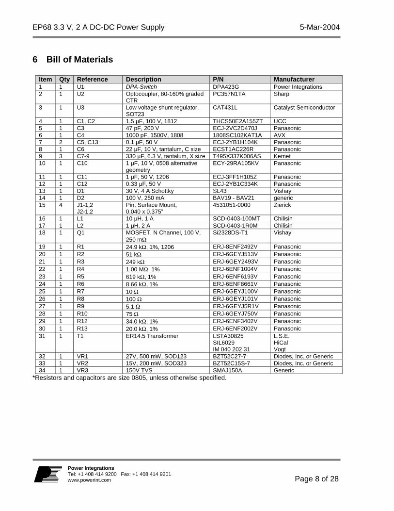
6 Bill of Materials
Item Qty Reference Description P/N Manufacturer 1 1 U1 DPA-Switch DPA423G Power Integrations 2 1 U2 Optocoupler, 80-160% graded
CTR PC357N1TA Sharp
3 1 U3 Low voltage shunt regulator, SOT23
CAT431L Catalyst Semiconductor
4 1 C1, C2 1.5 µF, 100 V, 1812 THCS50E2A155ZT UCC 5 1 C3 47 pF, 200 V ECJ-2VC2D470J Panasonic 6 1 C4 1000 pF, 1500V, 1808 1808SC102KAT1A AVX 7 2 C5, C13 0.1 µF, 50 V ECJ-2YB1H104K Panasonic 8 1 C6 22 µF, 10 V, tantalum, C size ECST1AC226R Panasonic 9 3 C7-9 330 µF, 6.3 V, tantalum, X size T495X337K006AS Kemet 10 1 C10 1 µF, 10 V, 0508 alternative
geometry ECY-29RA105KV Panasonic
11 1 C11 1 µF, 50 V, 1206 ECJ-3FF1H105Z Panasonic 12 1 C12 0.33 µF, 50 V ECJ-2YB1C334K Panasonic 13 1 D1 30 V, 4 A Schottky SL43 Vishay 14 1 D2 100 V, 250 mA BAV19 - BAV21 generic 15 4 J1-1,2
J2-1,2 Pin, Surface Mount, 0.040 x 0.375”
4531051-0000 Zierick
16 1 L1 10 µH, 1 A SCD-0403-100MT Chilisin 17 1 L2 1 µH, 2 A SCD-0403-1R0M Chilisin 18 1 Q1 MOSFET, N Channel, 100 V,
250 mΩ Si2328DS-T1 Vishay
19 1 R1 24.9 kΩ, 1%, 1206 ERJ-8ENF2492V Panasonic 20 1 R2 51 kΩ ERJ-6GEYJ513V Panasonic 21 1 R3 249 kΩ ERJ-6GEY2493V Panasonic 22 1 R4 1.00 MΩ, 1% ERJ-6ENF1004V Panasonic 23 1 R5 619 kΩ, 1% ERJ-6ENF6193V Panasonic 24 1 R6 8.66 kΩ, 1% ERJ-6ENF8661V Panasonic 25 1 R7 10 Ω ERJ-6GEYJ100V Panasonic 26 1 R8 100 Ω ERJ-6GEYJ101V Panasonic 27 1 R9 5.1 Ω ERJ-6GEYJ5R1V Panasonic 28 1 R10 75 Ω ERJ-6GEYJ750V Panasonic 29 1 R12 34.0 kΩ, 1% ERJ-6ENF3402V Panasonic 30 1 R13 20.0 kΩ, 1% ERJ-6ENF2002V Panasonic 31 1 T1 ER14.5 Transformer LSTA30825
SIL6029 IM 040 202 31
L.S.E. HiCal Vogt
32 1 VR1 27V, 500 mW, SOD123 BZT52C27-7 Diodes, Inc. or Generic 33 1 VR2 15V, 200 mW, SOD323 BZT52C15S-7 Diodes, Inc. or Generic 34 1 VR3 150V TVS SMAJ150A Generic
*Resistors and capacitors are size 0805, unless otherwise specified.

5-Mar-2004 EP68 3.3 V, 2 A DC-DC Power Supply
Page 9 of 28
Power IntegrationsTel: +1 408 414 9200 Fax: +1 408 414 9201
www.powerint.com
7 Transformer Specification
7.1 Electrical Diagram
WDG #32T #28 AWG x2
WDG #110T #34 AWG WDG #2
8T #34 AWG
WDG #410T #34 AWG
1
2
3
9,10
6,7
4
5
ER14.5 3C96 / 3F3,10 pin Bobbin
Figure 5 - Transformer Electrical Diagram.
7.2 Electrical Specifications
Electrical Strength 1 second, 60 Hz, from Pins 1-5 to Pins 6-10 1500 VDC
Primary Inductance Pins 1-3, all other windings open 120 µH,
+/-10% Resonant Frequency Pins 1-3, all other windings open 7.5 MHz (min.) Primary Leakage Inductance Pins 1-3, with Pins 6/7-9/10 shorted 3.0 µH (max.)
7.3 Materials Item Description [1] Core: ER14.5, Ferroxcube 3C96, 3F3 (or equivalent), ALG = 312 nH/T2 [2] Bobbin: ER14.5, 10 pin [3] Magnet Wire: #34 AWG, Double Coated (Heavy Nyleze) [4] Magnet Wire: #28 AWG, Double Coated (Heavy Nyleze) [5] Tape: 3M 1298 Polyester Film (or equivalent), 1.8 mm wide [6] Core Clamp ER14.5 Ferroxcube CLM14.5 (optional) [7] Varnish (DIPPED ONLY, NOT IMPREGNATED)

EP68 3.3 V, 2 A DC-DC Power Supply 5-Mar-2004
Page 10 of 28
Power Integrations Tel: +1 408 414 9200 Fax: +1 408 414 9201 www.powerint.com
7.4 Transformer Build Diagram
3
4
2
5
1
1/2 Primary
Bias
Secondary
1/2 Primary
Tape
Tape
Pin Side
Tape
6,7
9,10
Figure 6 - Transformer Build Diagram.
7.5 Transformer Construction
Bobbin Preparation Arrange bobbin & rotation such that primary start/finish wires do not overlap.
½ Primary Start at Pin 3. Wind 10 turns of item [3] in 1 layer. Bring finish lead back and terminate on Pin 2.
Bias Winding Starting at Pin 4, wind 8 turns of item [3]. Spread turns evenly across bobbin in a single layer. Bring finish lead back and terminate on Pin 5.
Basic Insulation Use one layer of item [5] for basic insulation.
Secondary Winding Start at Pins 9 and 10. Wind 2 turns of bifilar item [4] in 1 layer. Bring finish lead back and terminate on Pins 6 and 7.
Basic Insulation Use one layer of item [5] for basic insulation.
½ Primary Continue from Pin 2. Wind 10 turns of item [3] in 1 layer. Bring finish lead back and terminate on Pin 1.
Outer Insulation Use one layer of item [5] for basic insulation.
Final Assembly Assemble and secure (glue or clamp, item[6]) core halves. Dip varnish item [7] and cure.

5-Mar-2004 EP68 3.3 V, 2 A DC-DC Power Supply
Page 11 of 28
Power IntegrationsTel: +1 408 414 9200 Fax: +1 408 414 9201
www.powerint.com
8 Transformer Spreadsheet
EP68 3.3 V, 2 A DC-DC Power Supply 5-Mar-2004
Page 12 of 28
Power Integrations Tel: +1 408 414 9200 Fax: +1 408 414 9201 www.powerint.com
5-Mar-2004 EP68 3.3 V, 2 A DC-DC Power Supply
Page 13 of 28
Power IntegrationsTel: +1 408 414 9200 Fax: +1 408 414 9201
www.powerint.com
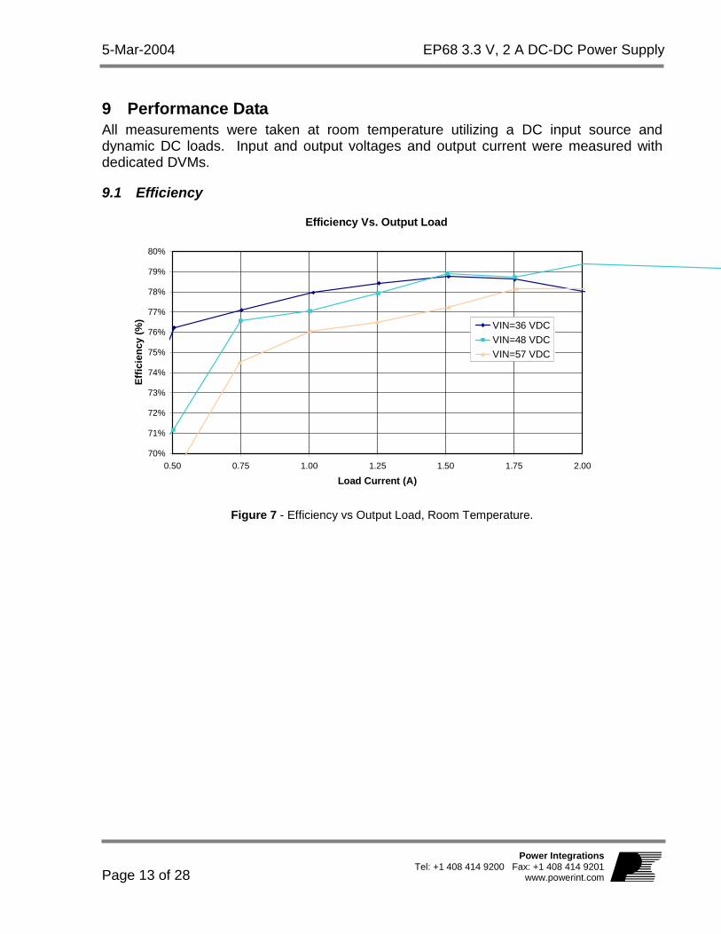
9 Performance Data All measurements were taken at room temperature utilizing a DC input source and dynamic DC loads. Input and output voltages and output current were measured with dedicated DVMs.
9.1 Efficiency
Figure 7 - Efficiency vs Output Load, Room Temperature.
Efficiency Vs. Output Load
70%
71%
72%
73%
74%
75%
76%
77%
78%
79%
80%
0.50 0.75 1.00 1.25 1.50 1.75 2.00
Load Current (A)
Eff
icie
ncy
(%
)
VIN=36 VDCVIN=48 VDCVIN=57 VDC

EP68 3.3 V, 2 A DC-DC Power Supply 5-Mar-2004
Page 14 of 28
Power Integrations Tel: +1 408 414 9200 Fax: +1 408 414 9201 www.powerint.com
9.2 Regulation
9.2.1 Load
Figure 8 - Load Regulation, Room Temperature.
9.2.2 Line
Figure 9 - Line Regulation, Room Temperature.
Load Regulation
3.20
3.25
3.30
3.35
3.40
0.0 0.3 0.5 0.8 1.0 1.3 1.5 1.8 2.0
Load Current (A)
Ou
tpu
t V
olt
age
(VD
C)
VIN=36 VDC
VIN=48 VDC
VIN=57 VDC
Line Regulation
3.20
3.25
3.30
3.35
3.40
30.0 40.0 50.0 60.0
Input Voltage (VDC)
Ou
tpu
t V
olt
age
(VD
C)
Full Load (2 A)
50% Load (1 A)
No Load

5-Mar-2004 EP68 3.3 V, 2 A DC-DC Power Supply
Page 15 of 28
Power IntegrationsTel: +1 408 414 9200 Fax: +1 408 414 9201
www.powerint.com
9.3 Peak Power The DC output load current was recorded just prior to the auto-restart operation.
Figure 10 - Maximum Output Overload Current, Room Temperature.
10 Waveforms
10.1 Drain Voltage and Current, Full Load Operation
Figure 11 – 36 VDC, Full Load.
Upper: IDRAIN, 0.5 A / div. Lower: VDRAIN, 50 V, 1 µs / div.
Figure 12 – 57 VDC, Full Load. Upper: IDRAIN, 0.5 A / div. Lower: VDRAIN, 50 V, 1 µs / div.
Maximum Output Current
2.50
2.60
2.70
2.80
2.90
3.00
30.0 40.0 50.0 60.0
Input Voltage (VDC)
Ou
tpu
t C
urr
ent
(A)
EP68 3.3 V, 2 A DC-DC Power Supply 5-Mar-2004
Page 16 of 28
Power Integrations Tel: +1 408 414 9200 Fax: +1 408 414 9201 www.powerint.com
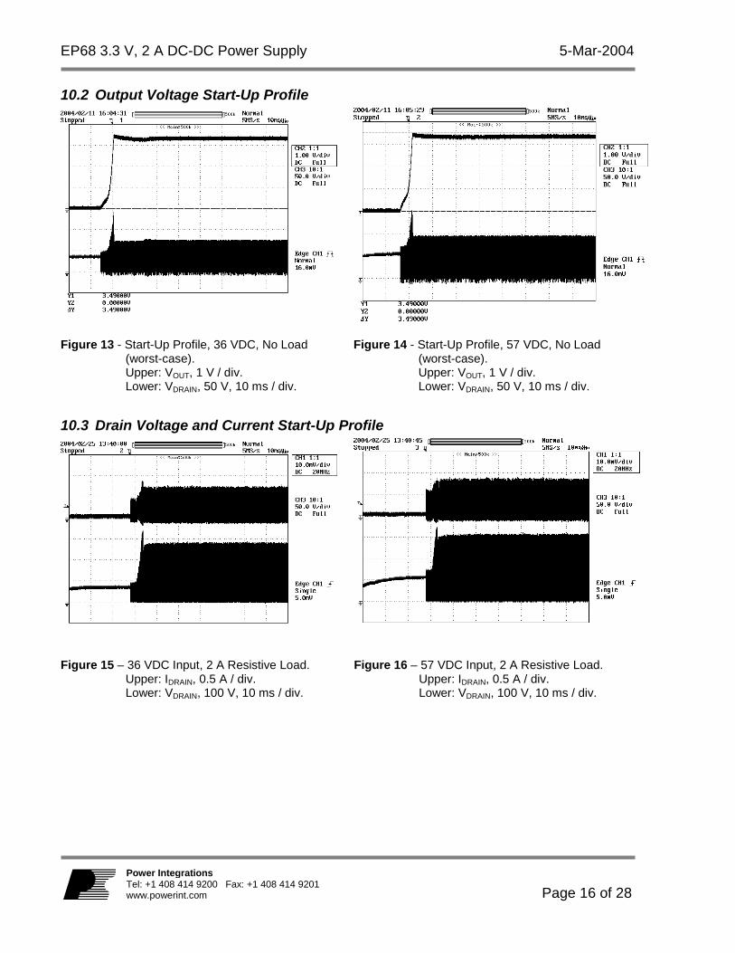
10.2 Output Voltage Start-Up Profile
Figure 13 - Start-Up Profile, 36 VDC, No Load (worst-case). Upper: VOUT, 1 V / div. Lower: VDRAIN, 50 V, 10 ms / div.
Figure 14 - Start-Up Profile, 57 VDC, No Load (worst-case). Upper: VOUT, 1 V / div. Lower: VDRAIN, 50 V, 10 ms / div.
10.3 Drain Voltage and Current Start-Up Profile
Figure 15 – 36 VDC Input, 2 A Resistive Load.
Upper: IDRAIN, 0.5 A / div. Lower: VDRAIN, 100 V, 10 ms / div.
Figure 16 – 57 VDC Input, 2 A Resistive Load. Upper: IDRAIN, 0.5 A / div. Lower: VDRAIN, 100 V, 10 ms / div.

5-Mar-2004 EP68 3.3 V, 2 A DC-DC Power Supply
Page 17 of 28
Power IntegrationsTel: +1 408 414 9200 Fax: +1 408 414 9201
www.powerint.com
10.4 Load Transient Response (75% to 100% Load Step) In the following two oscilloscope screen shots (Figures 17 and 18), signal averaging was used to more clearly capture the output voltage response to a load transient. Averaging minimizes the appearance of the 400 kHz switching ripple in the output voltage scope plot. The load current step was used to trigger the horizontal sweep of the oscilloscope.
Figure 17 - Transient Response,
36 VDC, 75-100-75% Load Step. Top: Load Current, 1 A / div. Bottom: Output Voltage, 20 mV, 500 µs / div.
Figure 18 - Transient Response, 57 VDC, 75-100-75% Load Step. Top: Load Current, 1 A / div. Bottom: Output Voltage, 20 mV, 500 µs / div.

EP68 3.3 V, 2 A DC-DC Power Supply 5-Mar-2004
Page 18 of 28
Power Integrations Tel: +1 408 414 9200 Fax: +1 408 414 9201 www.powerint.com
10.5 Output Ripple Measurements
10.5.1 Ripple Measurement Technique For DC output ripple measurements, a modified oscilloscope test probe must be utilized in order to reduce spurious signals due to pickup. Details of the probe modification are provided in Figures 19 and 20. The 5125BA probe adapter is affixed with two capacitors tied in parallel across the probe tip. The capacitors include one (1) 0.1 µF/50 V ceramic type and one (1) 1.0 µF/50 V aluminum electrolytic. The aluminum electrolytic type capacitor is polarized, so proper polarity across DC outputs must be maintained (see below).
Figure 19 - Oscilloscope Probe Prepared for Ripple Measurement (End Cap and Ground Lead Removed).
Figure 20 - Oscilloscope Probe with Probe Master 5125BA BNC Adapter (Modified with Wires for Probe
Ground for Ripple Measurement, and Two Parallel Decoupling Capacitors Added).
Probe Ground
Probe Tip

5-Mar-2004 EP68 3.3 V, 2 A DC-DC Power Supply
Page 19 of 28
Power IntegrationsTel: +1 408 414 9200 Fax: +1 408 414 9201
www.powerint.com
10.5.2 Output Ripple Measurements
Figure 21 - Ripple, 36 VDC, Full Load. Top: 10 mV / div, 50 µs / div. Bottom: 10 mV / div, 2 µs / div.
Figure 22 - Ripple, 48 VDC, Full Load. Top: 10 mV / div, 50 µs / div. Bottom: 10 mV / div, 2 µs / div.
Figure 23 - Ripple, 57 VDC, Full Load.
Top: 10 mV / div, 50 µs / div. Bottom: 10 mV / div, 2 µs / div.

EP68 3.3 V, 2 A DC-DC Power Supply 5-Mar-2004
Page 20 of 28
Power Integrations Tel: +1 408 414 9200 Fax: +1 408 414 9201 www.powerint.com
11 Thermal Performance The temperatures of key components were recorded using T-type thermocouples. Two of the four thermocouples were soldered; one directly to a SOURCE pin of the DPA423G (U1) and the other to the cathode of the output rectifier (D1). The other two thermocouples were glued; one to the transformer (T1) core, on the center leg, and the other to the case of the first (of the two) high-ripple output capacitor (C7). The unit was operated at full load, at 36 VDC, 48 VDC and 57 VDC, in free convection within a small enclosure. The results show adequate thermal margin, considering an additional ambient rise of +28 °C, equivalent to operating at an ambient of 50 °C. At 36 VDC, full load, within an enclosure at 50 °C ambient, this equates to a DPA423G case temperature of 79 °C. This is well below the recommended maximum case temperature of 100 °C. Figure 24 is an infrared thermograph taken at nominal-line (48 VDC).
Measured Temperature (°C)
Item 36 VDC 48 VDC 57 VDC
Ambient 22 22 22
DPA423G (U1) 51 51 53
Transformer core (T1) 75 75 75
Output Rectifier (D1) 63 61 61
Output Capacitor (C7) 45 43 43

5-Mar-2004 EP68 3.3 V, 2 A DC-DC Power Supply
Page 21 of 28
Power IntegrationsTel: +1 408 414 9200 Fax: +1 408 414 9201
www.powerint.com
TOP VIEW
BOTTOM VIEW
Figure 24- Infrared Thermograph of the EP68 Board, 48 VDC, Full Load, Room Ambient.

EP68 3.3 V, 2 A DC-DC Power Supply 5-Mar-2004
Page 22 of 28
Power Integrations Tel: +1 408 414 9200 Fax: +1 408 414 9201 www.powerint.com
12 Control Loop Measurements
12.1 36 VDC Maximum and Nominal Load
Figure 25 - Gain-Phase Plot, 36 VDC, Maximum Load (2 A).
Vertical Scale: Gain = 10 dB / div, Phase = 30° / div. Crossover Frequency = 10.0 kHz, Phase Margin = 60°
Figure 26 - Gain-Phase Plot, 36 VDC, Light Load (100 mA).
Vertical Scale: Gain = 10 dB / div, Phase = 30° / div. Crossover Frequency = 0.9 kHz, Phase Margin = 65°

5-Mar-2004 EP68 3.3 V, 2 A DC-DC Power Supply
Page 23 of 28
Power IntegrationsTel: +1 408 414 9200 Fax: +1 408 414 9201
www.powerint.com
12.2 57 VDC Maximum Load
Figure 27 - Gain-Phase Plot, 57 VDC, Light Load (100 mA).
Vertical Scale: Gain = 10 dB / div, Phase = 30° / div. Crossover Frequency = 10.8 kHz, Phase Margin = 40°
Figure 28 - Gain-Phase Plot, 57 VDC, Light Load (100 mA).
Vertical Scale: Gain = 10 dB / div, Phase = 30° / div. Crossover Frequency = 0.9 kHz, Phase Margin = 60°
The results indicate adequate loop bandwidth and significant gain and phase margin.

EP68 3.3 V, 2 A DC-DC Power Supply 5-Mar-2004
Page 24 of 28
Power Integrations Tel: +1 408 414 9200 Fax: +1 408 414 9201 www.powerint.com
13 Revision History
Date Author Revision Description & changes 25-Feb-04 SH 0.1 First release 02-Mar-04 PV 0.2 Second release after minor edits 15-Mar-04 PV 1.0 Final release

5-Mar-2004 EP68 3.3 V, 2 A DC-DC Power Supply
Page 25 of 28
Power IntegrationsTel: +1 408 414 9200 Fax: +1 408 414 9201
www.powerint.com
Notes

EP68 3.3 V, 2 A DC-DC Power Supply 5-Mar-2004
Page 26 of 28
Power Integrations Tel: +1 408 414 9200 Fax: +1 408 414 9201 www.powerint.com
Notes
Notes

5-Mar-2004 EP68 3.3 V, 2 A DC-DC Power Supply
Page 27 of 28
Power IntegrationsTel: +1 408 414 9200 Fax: +1 408 414 9201
www.powerint.com
Notes
EP68 3.3 V, 2 A DC-DC Power Supply 5-Mar-2004
Page 28 of 28
Power Integrations Tel: +1 408 414 9200 Fax: +1 408 414 9201 www.powerint.com
For the latest updates, visit our Web site: www.powerint.com Power Integrations may make changes to its products at any time. Power Integrations has no liability arising from your use of any information, device or circuit described herein nor does it convey any license under its patent rights or the rights of others. POWER INTEGRATIONS MAKES NO WARRANTIES HEREIN AND SPECIFICALLY DISCLAIMS ALL WARRANTIES INCLUDING, WITHOUT LIMITATION, THE IMPLIED WARRANTIES OF MERCHANTABILITY, FITNESS FOR A PARTICULAR PURPOSE, AND NON-INFRINGEMENT OF THIRD PARTY RIGHTS. PATENT INFORMATION The products and applications illustrated herein (including circuits external to the products and transformer construction) may be covered by one or more U.S. and foreign patents or potentially by pending U.S. and foreign patent applications assigned to Power Integrations. A complete list of Power Integrations’ patents may be found at www.powerint.com. The PI Logo, TOPSwitch, TinySwitch, LinkSwitch, and EcoSmart are registered trademarks of Power Integrations. PI Expert and DPA-Switch are trademarks of Power Integrations. © Copyright 2004, Power Integrations. WORLD HEADQUARTERS Power Integrations 5245 Hellyer Avenue San Jose, CA 95138, USA. Main: +1-408-414-9200 Customer Service: Phone: +1-408-414-9665 Fax: +1-408-414-9765 e-mail: [email protected]
CHINA (SHENZHEN) Power Integrations International Holdings, Inc. Rm# 1705, Bao Hua Bldg. 1016 Hua Qiang Bei Lu Shenzhen Guangdong, 518031, China Phone: +86-755-8367-5143 Fax: +86-755-8377-9610 e-mail: [email protected]
ITALY Power Integrations S.r.l. Via Vittorio Veneto 12, Bresso Milano, 20091, Italy Phone: +39-028-928-6001 Fax: +39-028-928-6009 e-mail: [email protected]
SINGAPORE (ASIA PACIFIC HEADQUARTERS) Power Integrations, Singapore 51 Newton Road #15-08/10 Goldhill Plaza Singapore, 308900 Phone: +65-6358-2160 Fax: +65-6358-2015 e-mail: [email protected]
AMERICAS Power Integrations 4335 South Lee Street, Suite G Buford, GA 30518, USA Phone: +1-678-714-6033 Fax: +1-678-714-6012 e-mail: [email protected]
GERMANY Power Integrations, GmbH Rueckertstrasse 3 D-80336, Muenchen, Germany Phone: +49-89-5527-3910 Fax: +49-89-5527-3920 e-mail: [email protected]
JAPAN Power Integrations, K.K. Keihin-Tatemono 1st Bldg. 12-20 Shin-Yokohama 2-Chome, Kohoku-ku, Yokohama-shi, Kanagawa 222-0033, Japan Phone: +81-45-471-1021 Fax: +81-45-471-3717 e-mail: [email protected]
TAIWAN Power Integrations International Holdings, Inc. 5F-1, No. 316, Nei Hu Rd., Sec. 1 Nei Hu Dist. Taipei, Taiwan 114, R.O.C. Phone: +886-2-2659-4570 Fax: +886-2-2659-4550 e-mail: [email protected]
CHINA (SHANGHAI) Power Integrations International Holdings, Inc. Rm 807, Pacheer Commercial Centre 555 Nanjing West Road Shanghai, 200041, China Phone: +86-21-6215-5548 Fax: +86-21-6215-2468 e-mail: [email protected]
INDIA (TECHNICAL SUPPORT) Innovatech 261/A, Ground Floor 7th Main, 17th Cross, Sadashivanagar Bangalore 560080 Phone: +91-80-5113-8020 Telefax: +91-80-5113-8023 e-mail: [email protected]
KOREA Power Integrations International Holdings, Inc. 8th Floor, DongSung Bldg. 17-8 Yoido-dong, Youngdeungpo-gu, Seoul, 150-874, Korea Phone: +82-2-782-2840 Fax: +82-2-782-4427 e-mail: [email protected]
UK (EUROPE & AFRICA HEADQUARTERS) Power Integrations (Europe) Ltd. 1st Floor, St. James’s House East Street Farnham Surrey GU9 7TJ United Kingdom Phone: +44 (0) 1252-730-140 Fax: +44 (0) 1252-727-689 e-mail: [email protected]
APPLICATIONS HOTLINE World Wide +1-408-414-9660
APPLICATIONS FAX World Wide +1-408-414-9760