6-Channel White LED Driver for up to 72...
35
○Product structure:Silicon monolithic integrated circuit ○This product is not designed protection against radioactive rays 1/32 TSZ02201-0G3G0C400180-1-2 07.Nov.2016 Rev.002 © 2012 ROHM Co., Ltd. All rights reserved. www.rohm.com TSZ22111・14・001 6-Channel White LED Driver for up to 72 LEDs BD6583MUV-A ●General Description BD6583MUV-A is white LED driver IC with PWM step-up DC/DC converter that can boost max 42.5V and current driver that can drive max 25mA. The wide and precision brightness can be controlled by external PWM pulse. BD6583MUV-A has very accurate current drivers, and it has few current errors between each strings. So, it will be helpful to reduce brightness spots on the LCD. Small package type is suited for saving space. ●Features High efficiency PWM step-up DC/DC converter (fsw=1MHz), max efficiency 93% High accuracy & good matching (±3%) current drivers 6ch Drive up to 12 * in series, 6 strings in parallel =72 white LEDs ( * white LED Vf=3.5Vmax) Rich safety functions ▪ Over-voltage protection (OVP) ▪ Over current limit ▪ External SBD open detect ▪ Thermal shutdown ●Key Specifications Operating power supply voltage range: 2.7V to 22.0V LED Maximum Current: 25mA (Max.) Quiescent Current 1: 0.6μA (Typ.) Quiescent Current 2: 4.6μA (Typ.) Operating temperature range: -30℃ to +85℃ ●Package W(Typ.) x T(Typ.) x H(Max.) ●Applications All middle size LCD equipments backlight of Notebook PC, portable DVD player, car navigation systems, etc. ●Typical Application Circuit 10μ F Battery VDET SW LED1 LED2 LED3 4.7μ H 10LED x 6parallel SENSP SENSN LED4 Each 20mA 100mΩ RTR020N05 2.2 μ F RSTB PWMPOW PWMDRV Power ON/OFF 200Hz PWM VBAT LED5 LED6 FAILSEL GND 24kΩ TEST GND ISETH VREG 1μF ISETL GND GND Figure 2. Typical Application Circuit BD6583MUV-A VQFN024V4040 4.00mm x 4.00mm x 1.00mm Figure 1. Package Figure 2. Typical Application Circuit
Transcript of 6-Channel White LED Driver for up to 72...

Product structure:Silicon monolithic integrated circuit This product is not designed protection against radioactive rays
1/32
TSZ02201-0G3G0C400180-1-207.Nov.2016 Rev.002
© 2012 ROHM Co., Ltd. All rights reserved. www.rohm.com
TSZ22111・14・001
Datasheet6-Channel White LED Driver for up to 72 LEDs BD6583MUV-A
General Description
BD6583MUV-A is white LED driver IC with PWM step-up DC/DC converter that can boost max 42.5V and current driver that can drive max 25mA. The wide and precision brightness can be controlled by external PWM pulse. BD6583MUV-A has very accurate current drivers, and it has few current errors between each strings. So, it will be helpful to reduce brightness spots on the LCD. Small package type is suited for saving space.
Features High efficiency PWM step-up DC/DC converter
(fsw=1MHz), max efficiency 93% High accuracy & good matching (±3%) current
drivers 6ch Drive up to 12* in series, 6 strings in parallel =72
white LEDs (*white LED Vf=3.5Vmax) Rich safety functions Over-voltage protection (OVP) Over current limit External SBD open detect Thermal shutdown
Key Specifications Operating power supply voltage range: 2.7V to 22.0V LED Maximum Current: 25mA (Max.) Quiescent Current 1: 0.6µA (Typ.) Quiescent Current 2: 4.6µA (Typ.) Operating temperature range: -30 to +85
Package W(Typ.) x T(Typ.) x H(Max.) Applications
All middle size LCD equipments backlight of Notebook PC, portable DVD player, car navigation systems, etc.
Typical Application Circuit
10µF
Battery
VDET SW
LED1
LED2
LED3
4.7µH 10LED x 6parallel
SENSP
SENSN
LED4
Each 20mA
100mΩ
RTR020N05
2.2µF
RSTB
PWMPOW
PWMDRV
Power ON/OFF
200HzPWM
VBAT
LED5
LED6
FAILSEL
GND 24kΩ
TEST
GND
ISETH
VREG 1µF
ISETL GND
GND
Figure 2. Typical Application Circuit
BD6583MUV-A
VQFN024V4040 4.00mm x 4.00mm x 1.00mm
Figure 1. Package
Figure 2. Typical Application Circuit
Datasheet
2/32
BD6583MUV-A
TSZ02201-0G3G0C400180-1-207.Nov.2016 Rev.002
© 2012 ROHM Co., Ltd. All rights reserved. www.rohm.com
TSZ22111・15・001
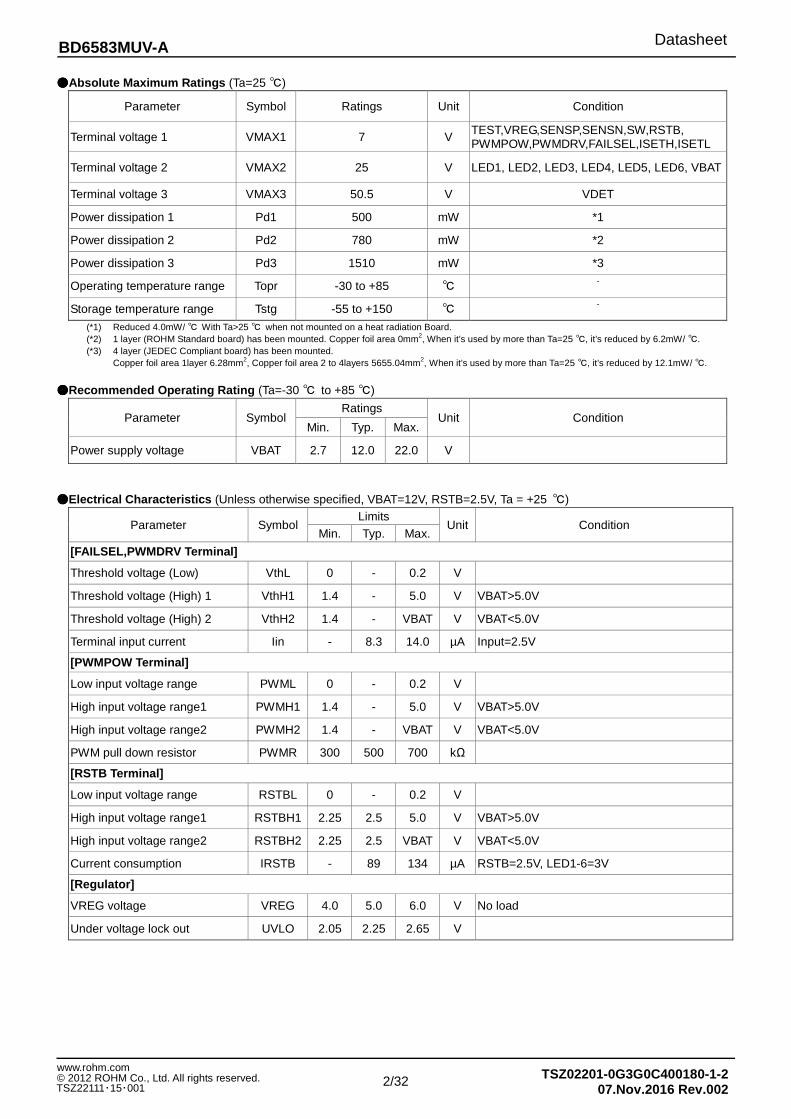
Absolute Maximum Ratings (Ta=25 )
Parameter Symbol Ratings Unit Condition
Terminal voltage 1 VMAX1 7 V TEST,VREG,SENSP,SENSN,SW,RSTB, PWMPOW,PWMDRV,FAILSEL,ISETH,ISETL
Terminal voltage 2 VMAX2 25 V LED1, LED2, LED3, LED4, LED5, LED6, VBAT
Terminal voltage 3 VMAX3 50.5 V VDET
Power dissipation 1 Pd1 500 mW *1
Power dissipation 2 Pd2 780 mW *2
Power dissipation 3 Pd3 1510 mW *3
Operating temperature range Topr -30 to +85 -
Storage temperature range Tstg -55 to +150 -
(*1) Reduced 4.0mW/ With Ta>25 when not mounted on a heat radiation Board.
(*2) 1 layer (ROHM Standard board) has been mounted. Copper foil area 0mm2, When it’s used by more than Ta=25 , it’s reduced by 6.2mW/ .
(*3) 4 layer (JEDEC Compliant board) has been mounted. Copper foil area 1layer 6.28mm2, Copper foil area 2 to 4layers 5655.04mm2, When it’s used by more than Ta=25
, it’s reduced by 12.1mW/ .
Recommended Operating Rating (Ta=-30
to +85 )
Parameter Symbol Ratings
Unit Condition Min. Typ. Max.
Power supply voltage VBAT 2.7 12.0 22.0 V
Electrical Characteristics (Unless otherwise specified, VBAT=12V, RSTB=2.5V, Ta = +25 )
Parameter Symbol Limits
Unit Condition Min. Typ. Max.
[FAILSEL,PWMDRV Terminal]
Threshold voltage (Low) VthL 0 - 0.2 V
Threshold voltage (High) 1 VthH1 1.4 - 5.0 V VBAT>5.0V
Threshold voltage (High) 2 VthH2 1.4 - VBAT V VBAT<5.0V
Terminal input current Iin - 8.3 14.0 µA Input=2.5V
[PWMPOW Terminal]
Low input voltage range PWML 0 - 0.2 V
High input voltage range1 PWMH1 1.4 - 5.0 V VBAT>5.0V
High input voltage range2 PWMH2 1.4 - VBAT V VBAT<5.0V
PWM pull down resistor PWMR 300 500 700 kΩ
[RSTB Terminal]
Low input voltage range RSTBL 0 - 0.2 V
High input voltage range1 RSTBH1 2.25 2.5 5.0 V VBAT>5.0V
High input voltage range2 RSTBH2 2.25 2.5 VBAT V VBAT<5.0V
Current consumption IRSTB - 89 134 µA RSTB=2.5V, LED1-6=3V
[Regulator]
VREG voltage VREG 4.0 5.0 6.0 V No load
Under voltage lock out UVLO 2.05 2.25 2.65 V

Datasheet
3/32
BD6583MUV-A
TSZ02201-0G3G0C400180-1-207.Nov.2016 Rev.002
© 2012 ROHM Co., Ltd. All rights reserved. www.rohm.com
TSZ22111・15・001
Electrical Characteristics - continued (Unless otherwise specified, VBAT=12V, RSTB=2.5V, Ta = +25 )
Parameter Symbol Limits
Unit Condition Min. Typ. Max.
[Switching Regulator]
Quiescent current 1 Iq1 - 0.6 3.4 µA RSTB=0V, VBAT=12V
Quiescent current 2 Iq2 - 4.6 10 µA RSTB=0V, VBAT=22V
Current consumption Idd - 3.4 5.1 mA VDET=0V,ISETH=24kΩ
LED control voltage VLED 0.4 0.5 0.6 V
Over current limit voltage Ocp 70 100 130 mV *1
SBD open protect Sop - - 0.1 V Detect voltage of VDET pin
Switching frequency fSW 0.8 1.0 1.2 MHz
Duty cycle limit Duty 92.5 95.0 99.0 % LED1-6=0.3V
Over voltage limit Ovl 43.0 44.7 46.4 V LED1-6=0.3V
[Current driver]
LED maximum current ILMAX - - 25 mA
LED current accuracy ILACCU - - ±5 % ILED=16mA
LED current matching ILMAT - - ±3 % Each LED current/Average (LED1- 6) ILED=16mA
ISET voltage Iset 0.5 0.6 0.7 V
LED current limiter ILOCP 35 60 90 mA Current limit value at ISET resistor 4.7kΩ setting LED1, 2, 3, 4, 5, 6=0.5V
LED terminal Over voltage protect LEDOVP 10.0 11.5 13.0 V RSTB=PWMDRV=2.5V *1 This parameter is tested with dc measurement.
Pin Descriptions
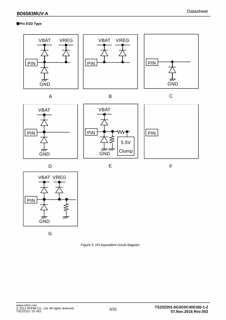
PIN Name In/Out PIN number Function Terminal equivalent
circuit diagram 1 VDET In Detect input for SBD open and OVP C 2 N.C. - No connect pin F 3 GND - GND B
4 SW Out Switching Tr drive terminal G 5 SENSP In + Side Current sense terminal G 6 TEST In TEST input (Pull down 100kΩ to GND) G
7 SENSN In - Side Current sense terminal A 8 GND - GND B
9 ISETH In Resistor connection for LED current setting at PWMDRV=H
A
10 ISETL In Resistor connection for LED current setting at PWMDRV=L
A
11 PWMDRV In PWM input pin for power ON/OFF only driver E 12 LED1 In Current sink for LED1 C 13 LED2 In Current sink for LED2 C
14 LED3 In Current sink for LED3 C 15 GND - GND B 16 LED4 In Current sink for LED4 C
17 LED5 In Current sink for LED5 C 18 LED6 In Current sink for LED6 C 19 FAILSEL In Latch selectable pin of protect function E
20 GND - GND B 21 RSTB In Reset pin L :Reset H :Reset cancel E 22 VREG Out Regulator output / Internal power-supply D
23 PWMPOW In PWM input pin for power ON/OFF E 24 VBAT In Battery input C
- Thermal PAD - Heat radiation PAD of back side Connect to GND -
Datasheet
4/32
BD6583MUV-A
TSZ02201-0G3G0C400180-1-207.Nov.2016 Rev.002
© 2012 ROHM Co., Ltd. All rights reserved. www.rohm.com
TSZ22111・15・001
Pin ESD Type
Figure 3. I/O equivalent circuit diagram
GND
VBAT VREG
PIN
A
VBAT
PIN
B
VREG
GND
PIN
C
GND
VBAT
PIN
D
GND
VBAT
PIN
E
5.5V
Clump
PIN
F
GND
VBAT
PIN
G
VREG
Datasheet
5/32
BD6583MUV-A
TSZ02201-0G3G0C400180-1-207.Nov.2016 Rev.002
© 2012 ROHM Co., Ltd. All rights reserved. www.rohm.com
TSZ22111・15・001
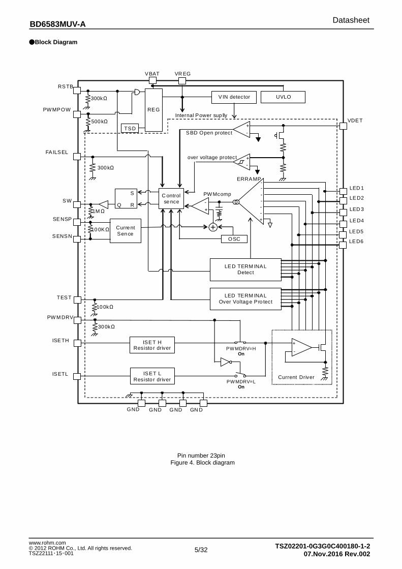
Block Diagram
Pin number 23pin Figure 4. Block diagram
Current Sen ce
S
Q R
- +
- +over voltage protect
SBD Open protect
V IN detector
REG Internal Power sup lly
VDET
SW
UVLO
RSTB
300kΩ
Current Driver
+
- - -
LED 1
LED2
LED 3
ERRAMP
+
+
-
OSC
C ontrol se nce
100kΩ
PW Mcomp
TEST
PWMPOW
SENSP
SENSN
LED4
-
1MΩ
10 0KΩ
LED TERM INAL Over Voltag e Pro tect
500kΩ
VBAT VR EG
FAILSEL
PW M DRV
- -
LED5
LED6
+
- PW MDRV=H On
ISET L Resisto r driver
PW MDRV=L
On
ISETH
ISETL
ISET H Resisto r driver
300kΩ
TSD
300kΩ
GND
GND
GND
GN D
LED TERM INAL Detect
Datasheet
6/32
BD6583MUV-A
TSZ02201-0G3G0C400180-1-207.Nov.2016 Rev.002
© 2012 ROHM Co., Ltd. All rights reserved. www.rohm.com
TSZ22111・15・001
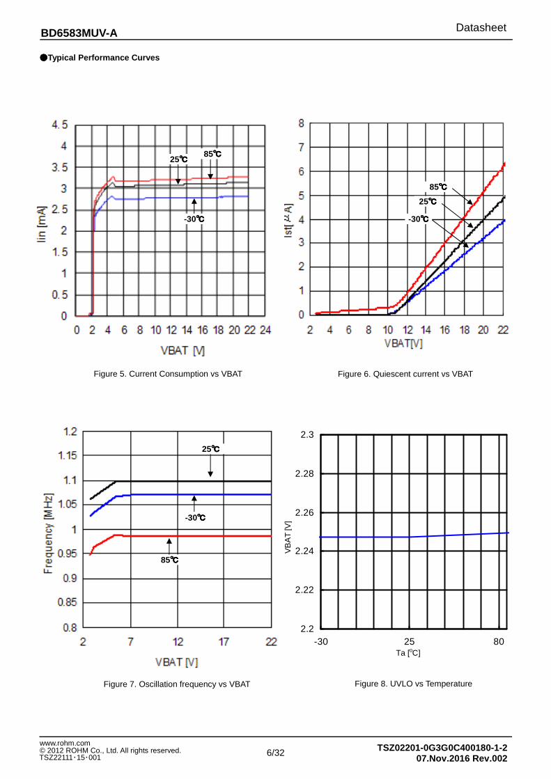
Typical Performance Curves
Figure 6. Quiescent current vs VBAT
Figure 8. UVLO vs Temperature
25
-30
85
2.2
2.22
2.24
2.26
2.28
2.3
-30 25 80Ta [oC]
VB
AT
[V]
-30
85
25
Figure 5. Current Consumption vs VBAT
Figure 7. Oscillation frequency vs VBAT
-30
25
85
25 85
-30
25
-30
85
Datasheet
7/32
BD6583MUV-A
TSZ02201-0G3G0C400180-1-207.Nov.2016 Rev.002
© 2012 ROHM Co., Ltd. All rights reserved. www.rohm.com
TSZ22111・15・001
Typical Performance Curves - Continued
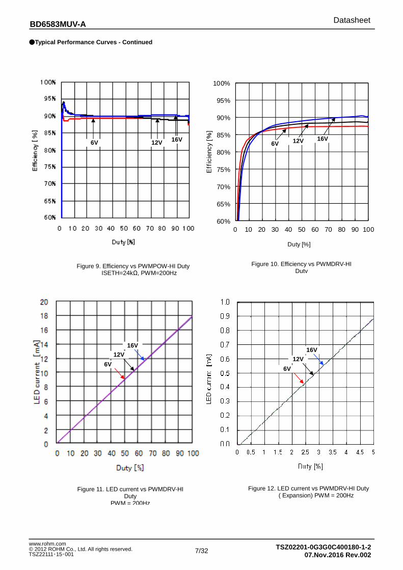
Figure 10. Efficiency vs PWMDRV-HI Duty
Figure 11. LED current vs PWMDRV-HI Duty
PWM = 200Hz
Figure 12. LED current vs PWMDRV-HI Duty ( Expansion) PWM = 200Hz
6V 12V 16V
60%
65%
70%
75%
80%
85%
90%
95%
100%
0 10 20 30 40 50 60 70 80 90 100
Eff
icie
ncy
[%]
Duty [%]
6V 12V 16V
6V
12V
16V
6V
12V
16V
Figure 9. Efficiency vs PWMPOW-HI Duty ISETH=24kΩ, PWM=200Hz

Datasheet
8/32
BD6583MUV-A
TSZ02201-0G3G0C400180-1-207.Nov.2016 Rev.002
© 2012 ROHM Co., Ltd. All rights reserved. www.rohm.com
TSZ22111・15・001
Typical Performance Curves - Continued
Figure 13. LED current vs PWMDRV-HI Duty PWM = 200Hz, 1kHz,10kHz
Figure 15. LED current vs PWMPOW-HI Duty TPWM = 200Hz
Figure 15. LED current vs PWMPOW-HI Duty ( Expansion) PWM = 200Hz
Figure 16. LED current vs PWMPOW-HI Duty PWM = 200Hz, 1kHz,10kHz
0
2
4
6
8
10
12
14
16
18
20
0 10 20 30 40 50 60 70 80 90 100
LE
D c
urr
en
t[m
A]
Duty [%]
6V
12V 16V
0.0
0.1
0.2
0.3
0.4
0.5
0.6
0.7
0.8
0.9
1.0
0 0.5 1 1.5 2 2.5 3 3.5 4 4.5 5
Duty (%)
LED
Cur
rent
[mA
]
6V
12V
16V
200Hz
1kHz
10kHz
Datasheet
9/32
BD6583MUV-A
TSZ02201-0G3G0C400180-1-207.Nov.2016 Rev.002
© 2012 ROHM Co., Ltd. All rights reserved. www.rohm.com
TSZ22111・15・001
Typical Performance Curves - Continued
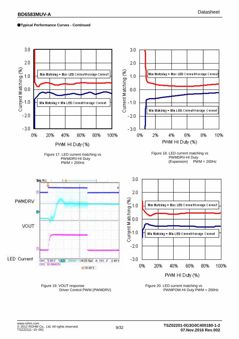
Figure 17. LED current matching vs PWMDRV-HI Duty
PWM = 200Hz
Figure 18. LED current matching vs PWMDRV-HI Duty
(Expansion) PWM = 200Hz
Figure 19. VOUT response Driver Control PWM (PWMDRV)
Figure 20. LED current matching vs PWMPOW-HI Duty PWM = 200Hz
Datasheet
10/32
BD6583MUV-A
TSZ02201-0G3G0C400180-1-207.Nov.2016 Rev.002
© 2012 ROHM Co., Ltd. All rights reserved. www.rohm.com
TSZ22111・15・001
Typical Performance Curves - Continued
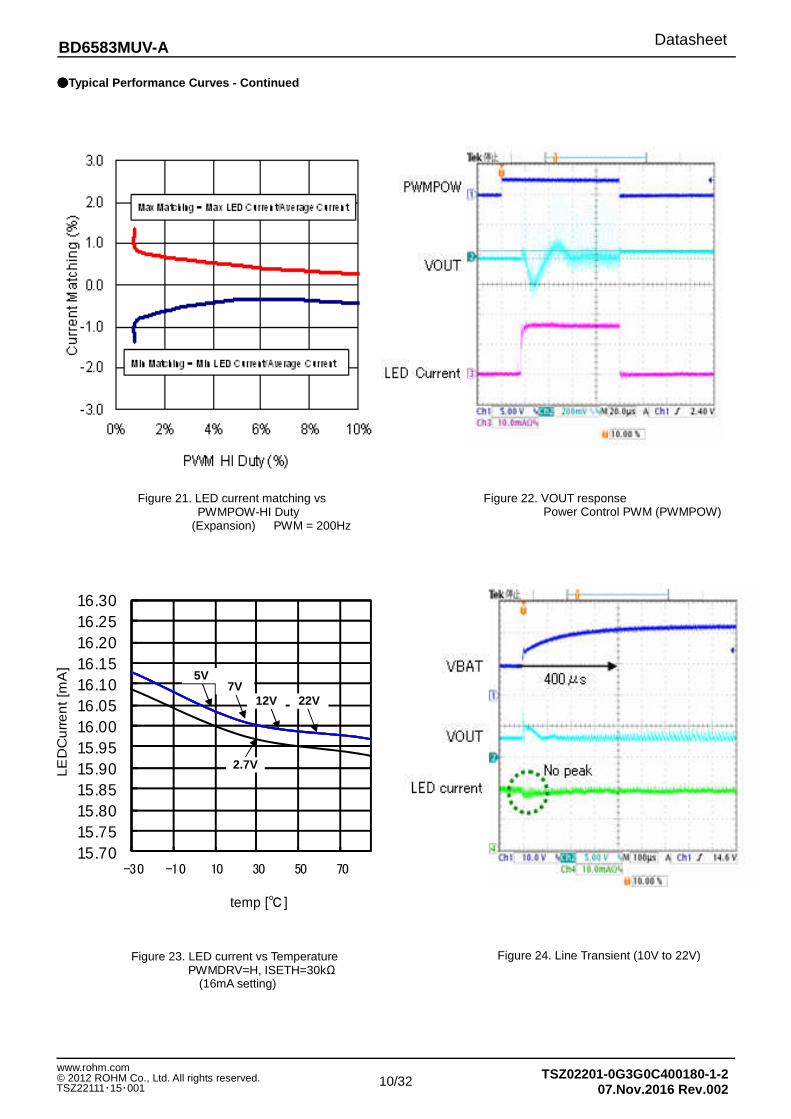
Figure 21. LED current matching vs PWMPOW-HI Duty
(Expansion) PWM = 200Hz
Figure 22. VOUT response Power Control PWM (PWMPOW)
Figure 24. Line Transient (10V to 22V)
Figure 23. LED current vs Temperature PWMDRV=H, ISETH=30kΩ
(16mA setting)
15.7015.7515.8015.8515.9015.9516.0016.0516.1016.1516.2016.2516.30
-30 -10 10 30 50 70
LE
DC
urr
en
t [m
A]
temp [ ]
2.7V
22V
5V 7V
12V

Datasheet
11/32
BD6583MUV-A
TSZ02201-0G3G0C400180-1-207.Nov.2016 Rev.002
© 2012 ROHM Co., Ltd. All rights reserved. www.rohm.com
TSZ22111・15・001
Typical Performance Curves - Continued
Figure 25. Line Transient (22V to 10V) Figure 26. VOUT@OVP(LED OPEN)
Datasheet
12/32
BD6583MUV-A
TSZ02201-0G3G0C400180-1-207.Nov.2016 Rev.002
© 2012 ROHM Co., Ltd. All rights reserved. www.rohm.com
TSZ22111・15・001
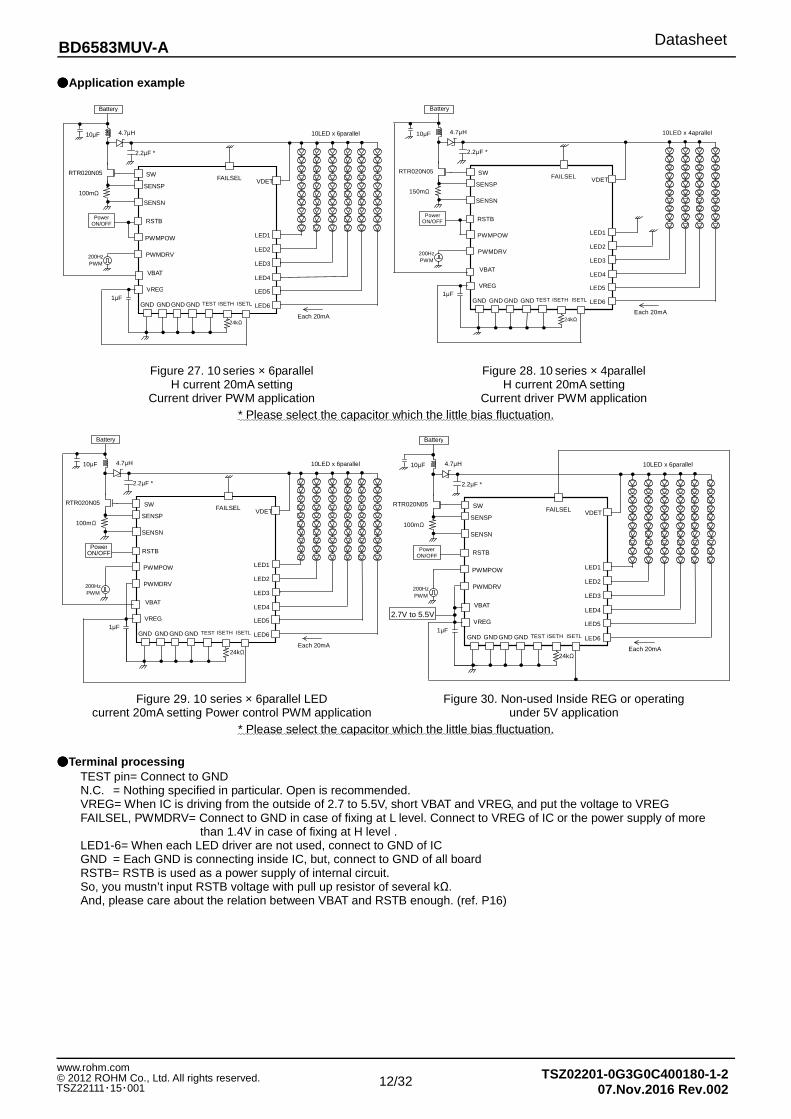
Application example
Figure 27. 10 series × 6parallel
H current 20mA setting Current driver PWM application
Figure 28. 10 series × 4parallel H current 20mA setting
Current driver PWM application * Please select the capacitor which the little bias fluctuation.
Figure 29. 10 series × 6parallel LED
current 20mA setting Power control PWM application Figure 30. Non-used Inside REG or operating
under 5V application * Please select the capacitor which the little bias fluctuation.
Terminal processing
TEST pin= Connect to GND N.C. = Nothing specified in particular. Open is recommended. VREG= When IC is driving from the outside of 2.7 to 5.5V, short VBAT and VREG, and put the voltage to VREG FAILSEL, PWMDRV= Connect to GND in case of fixing at L level. Connect to VREG of IC or the power supply of more
than 1.4V in case of fixing at H level . LED1-6= When each LED driver are not used, connect to GND of IC GND = Each GND is connecting inside IC, but, connect to GND of all board RSTB= RSTB is used as a power supply of internal circuit. So, you mustn’t input RSTB voltage with pull up resistor of several kΩ. And, please care about the relation between VBAT and RSTB enough. (ref. P16)
10µF
Battery
VDET SW
LED1
LED2
LED3
4.7µH 10LED x 6parallel
SENSP
SENSN
LED4
Each 20mA
100mΩ
RTR020N05
2.2µF *
RSTB
PWMPOW
PWMDRV
Power ON/OFF
200HzPWM
VBAT
LED5
LED6
FAILSEL
GND
24kΩ
TEST
GND
ISETH
VREG 1µF
ISETL GND
GND
10µF
Battery
VDET SW
LED1
LED2
LED3
4.7µH 10LED x 4aprallel
SENSP
SENSN
LED4
Each 20mA
150mΩ
RTR020N05
2.2µF *
RSTB
PWMPOW
PWMDRV
Power ON/OFF
200HzPWM
VBAT
LED5
LED6
FAILSEL
GND
24kΩ
TEST
GND
ISETH
VREG 1µF
ISETL GND
GND
10µF
Battery
VDET SW
LED1
LED2
LED3
4.7µH 10LED x 6parallel
SENSP
SENSN
LED4
Each 20mA
100mΩ
RTR020N05
2.2µF *
RSTB
PWMPOW
PWMDRV
Power ON/OFF
200HzPWM
VBAT
LED5
LED6
FAILSEL
GND
24kΩ
TEST
GND
ISETH
VREG 1µF
ISETL GND
GND
10µF
Battery
VDET SW
LED1
LED2
LED3
4.7µH 10LED x 6parallel
SENSP
SENSN
LED4
Each 20mA
100mΩ
RTR020N05
2.2µF *
RSTB
PWMPOW
PWMDRV
Power ON/OFF
200HzPWM
VBAT
LED5
LED6
FAILSEL
VREG 1µF
2.7V to 5.5V
GND
24kΩ
TEST
GND
ISETH
ISETL GND
GND

Datasheet
13/32
BD6583MUV-A
TSZ02201-0G3G0C400180-1-207.Nov.2016 Rev.002
© 2012 ROHM Co., Ltd. All rights reserved. www.rohm.com
TSZ22111・15・001
Description of Functions 1) PWM current mode DC/DC converter
While BD6583MUV-A is power ON, the lowest voltage of LED1, 2, 3, 4, 5, 6 is detected, PWM duty is decided to be 0.5Vand output voltage is kept invariably. As for the inputs of the PWM comparator as the feature of the PWM current mode, one is overlapped with error components from the error amplifier, and the other is overlapped with a current sense signal that controls the inductor current into Slope waveform to prevent sub harmonic oscillation. This output controls external Nch Tr via the RS latch. In the period where external Nch Tr gate is ON, energy is accumulated in the external inductor, and in the period where external Nch Tr gate is OFF, energy is transferred to the output capacitor via external SBD.BD6583MUV-A has many safety functions, and their detection signals stop switching operation at once.
2) Soft start
BD6583MUV-A has soft start function. The soft start function prevents large coil current. Rush current at turning on is prevented by the soft start function. After RSTB is changed L H, when PWMPOW is changed L H, soft start becomes effective for within 1ms and soft start doesn't become effective even if PWMPOW is changed L H after that. And, when the H section of PWMPOW is within 1ms, soft start becomes invalid when PWMPOW is input to H more than three times. The invalid of the soft start can be canceled by making RSTB L.
3) FAILSEL pin When the error condition occurs, boost operating is stopped by the protection function, and the error condition is avoided. On that occasion, the way to stop of boost operating by the protection function can be selected with FAILSEL pin. Details are as shown in Figure 31, 32. After power ON, when the protection function is operating under about 1ms have passed, the stop state of the boost operating can be held through FAILSEL is H, the stop state can reset through RSTB is L. And, boost operating is stopped when the protection function is operating through FAILSEL is L, but when the protection function becomes un-detect, boost operating is started again. It never keeps holding the stop state of boost operating.
Object of protect function is as shown below. ・ Over-voltage protection ・ External SBD open detect ・ Thermal shutdown ・ LED terminal over-voltage protection ・ Over current limit
Figure 31. FAILSEL operating description Figure 32. FAILSEL=H light off control
In PWM control by PWMDRV can ’t use this function. When it is off over 10ms on PWM control by PWMPOW usin g this function, it may be stopped the boost operating as over current protection work at off on PWMPOW=L.
RSTB
PWMDRV
Coil current
FAILSEL
functioninvalid valid
< When it is off on PWMPOW>
Output voltage
PWMPOW
RSTB
PWMDRV
PWMPOW
invalid
Output voltage
Coil current
FAILSEL
function
< When it is off on RSTB>
about 1ms
un-operating range FAILSEL
RSTB
Protection function
detection
Boost operating
normal operating off boost stop
“H”
off normal operating
un-detection un-detection
<FAILSEL=H>
about 1ms
un-operating range FAILSEL
RSTB
Protection function
normal operating off
un-detection detection
normal operating boost stop off normal
“L”
un-detectio
<FAILSEL=L>
Boost operating
Datasheet
14/32
BD6583MUV-A
TSZ02201-0G3G0C400180-1-207.Nov.2016 Rev.002
© 2012 ROHM Co., Ltd. All rights reserved. www.rohm.com
TSZ22111・15・001
4) External SBD open detect and over voltage protection BD6583MUV-A has over boost protection by external SBD open and over voltage protection. It detects VDET voltage and is stopped output Tr in abnormal condition. Details are as shown below. External SBD open detect In the case of external SBD is not connected to IC, the coil or external Tr may be destructed. Therefore, at such an error as VOUT becoming 0.1V or below, the Under Detector shown in the figure works, and turns off the output Tr, and prevents the coil and the IC from being destructed. And the IC changes from activation into non-activation, and current does not flow to the coil (0mA). Over voltage protection At such an error of output open as the output DC/DC and the LED is not connected to IC, the DC/DC will boost too much and the VDET terminal exceed the absolute maximum ratings, and may destruct the IC. Therefore, when VDET becomes sensing voltage or higher, the over voltage limit works, and turns off the output Tr, and the pressure up made stop. At this moment, the IC changes from activation into non-activation, and the output voltage goes down slowly. And, when the output voltage becomes the hysteresis of the over voltage limit or below, the output voltage pressure up to sensing voltage once again and unless the application error is recovered, this operation is repeated.
5) Thermal shut down BD6583MUV-A has thermal shut down function. The thermal shut down works at 175°C or higher, and the IC changes from activation into non-activation. Because non-activation is different from RSTB=L, it doesn’t’ be reset inside IC. Moreover, even if thermal shut down function works, soft start, FAILSEL, selection the number of LED lines of the current driver and starting current setting at PWMDRV=L related RSTB are hold.
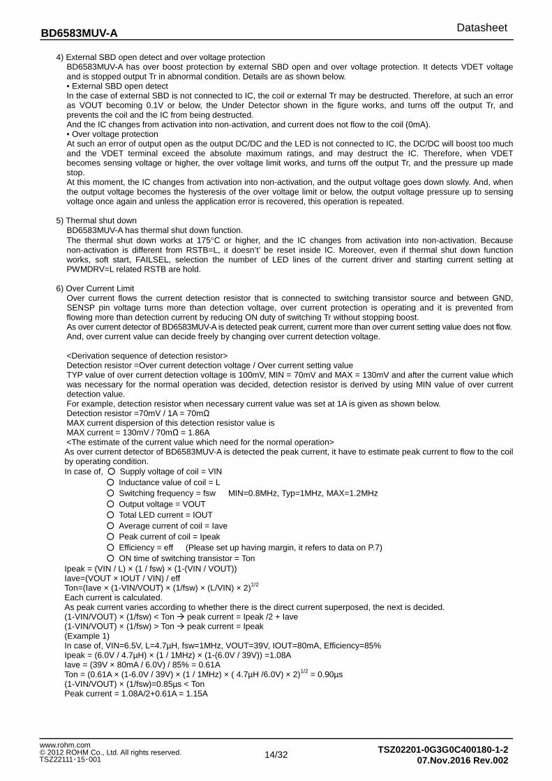
6) Over Current Limit Over current flows the current detection resistor that is connected to switching transistor source and between GND, SENSP pin voltage turns more than detection voltage, over current protection is operating and it is prevented from flowing more than detection current by reducing ON duty of switching Tr without stopping boost. As over current detector of BD6583MUV-A is detected peak current, current more than over current setting value does not flow. And, over current value can decide freely by changing over current detection voltage. <Derivation sequence of detection resistor> Detection resistor =Over current detection voltage / Over current setting value TYP value of over current detection voltage is 100mV, MIN = 70mV and MAX = 130mV and after the current value which was necessary for the normal operation was decided, detection resistor is derived by using MIN value of over current detection value. For example, detection resistor when necessary current value was set at 1A is given as shown below. Detection resistor =70mV / 1A = 70mΩ MAX current dispersion of this detection resistor value is MAX current = 130mV / 70mΩ = 1.86A <The estimate of the current value which need for the normal operation> As over current detector of BD6583MUV-A is detected the peak current, it have to estimate peak current to flow to the coil by operating condition. In case of, Supply voltage of coil = VIN Inductance value of coil = L Switching frequency = fsw MIN=0.8MHz, Typ=1MHz, MAX=1.2MHz Output voltage = VOUT Total LED current = IOUT Average current of coil = Iave Peak current of coil = Ipeak Efficiency = eff (Please set up having margin, it refers to data on P.7) ON time of switching transistor = Ton Ipeak = (VIN / L) × (1 / fsw) × (1-(VIN / VOUT)) Iave=(VOUT × IOUT / VIN) / eff Ton=(Iave × (1-VIN/VOUT) × (1/fsw) × (L/VIN) × 2)1/2 Each current is calculated. As peak current varies according to whether there is the direct current superposed, the next is decided. (1-VIN/VOUT) × (1/fsw) < Ton peak current = Ipeak /2 + Iave (1-VIN/VOUT) × (1/fsw) > Ton peak current = Ipeak (Example 1) In case of, VIN=6.5V, L=4.7µH, fsw=1MHz, VOUT=39V, IOUT=80mA, Efficiency=85% Ipeak = (6.0V / 4.7µH) × (1 / 1MHz) × (1-(6.0V / 39V)) =1.08A Iave = (39V × 80mA / 6.0V) / 85% = 0.61A Ton = (0.61A × (1-6.0V / 39V) × (1 / 1MHz) × ( 4.7µH /6.0V) × 2)1/2 = 0.90µs (1-VIN/VOUT) × (1/fsw)=0.85µs < Ton Peak current = 1.08A/2+0.61A = 1.15A

Datasheet
15/32
BD6583MUV-A
TSZ02201-0G3G0C400180-1-207.Nov.2016 Rev.002
© 2012 ROHM Co., Ltd. All rights reserved. www.rohm.com
TSZ22111・15・001
(Example 2) In case of, VIN=12.0V, L=4.7µH, fsw=1MHz, VOUT=39V, IOUT=80mA, Efficiency=85% Ipeak = (12.0V / 4.7µH) × (1 / 1MHz) × (1-(12V / 39V)) =1.77A Iave = (39V × 80mA / 12.0V) / 85% = 0.31A Ton = (0.31A × (1-12 V / 39V) × (1 / 1MHz) × ( 4.7µH /12 V) × 2)1/2 = 0.41µs (1-VIN/VOUT) × (1/fsw)=0.69µs > Ton Peak current = 12V/4.7µH × 0.41µs = 1.05A *When too large current is set, output overshoot is caused, be careful enough because it is led to break down of the IC in case of the worst.
Operating of the application deficiency
1) When 1 LED or 1parallel OPEN during the operating In case of FAILSEL=L, the LED parallel which became OPEN isn't lighting, but other LED parallel is lighting. At that time, output boosts up to the over voltage protection voltage 44.7V so that LED terminal may be 0V or it boost to the output voltage that LED terminal voltage becomes LED terminal over voltage protection 11.5V or it becomes the output voltage restricted by the over current limit. In case of FAILSEL=H, boost stops when LED becomes OPEN and all LED turns off the lights.
2) When LED short-circuited in the plural In case of FAILSEL=L, all LED is turned on unless LED terminal voltage is LED terminal over voltage protection of more than 11.5V. When it was more than 11.5V only the line which short-circuited is turned on normally and LED current of other lines fall or turn off the lights. In case of FAILSEL=H, boost stops at more than 11.5V and all LED turns off the lights.
3) When Schottky diode came off Regardless of FAILSEL, all LED isn't turned on. Also, IC and a switching transistor aren't destroyed because boost operating stops by the Schottky diode coming off protected function.
4) When over current detection resistor came off Regardless of FAILSEL, all LED isn't turned on. Because the resistance of 100kΩ is between SENSP and SENSN terminal, over current protection works instantly and LED current can't be flow.
Control signal input timing
Figure 33. Control signal timing Figure 34. Voltage with a control sign higher than VBAT Example corresponding to application of conditions
In case you input control signs, such as RSTB, PWMPOW, and PWMDRV, in the condition that the standup of supply voltage (VBAT) is not completed, be careful of the following point. ①Input each control signal after VBAT exceeds 2.7V. ②Please do not input each control sign until VBAT exceeds H voltage of RSTB, PWMPOW, and PWMDRV. ③When you input RSTB during the standup of VBAT and H voltage is inputted into PWMPOW, please give the standup time to stable voltage as Min.100µs 2.7V of VBAT. There is no timing limitation at each input signal of RSTB, PWMPOW and PWMDRV. If each control sign changes into a condition lower than VBAT in (1) and (2), it goes via the ESD custody diode by the side of VBAT of each terminal. A power supply is supplied to VBAT and there is a possibility of malfunctioning. Moreover, when the entrance current to the terminal exceeds 50mA, it has possibility to damage the LSI. In order to avoid this condition, as shown in the above figure, please insert about 220Ω in a signal line, and apply current qualification. Please confirm an internal pull down resistor in the block diagram and electrical property of P.5.
GND
VBAT
PIN
Rin
0V
5V 220Ω
RSTB
DC/DC VOUT
3
VREG
PWMDRV
PWMPOW
5V
Min. 100µs
2
5V
2.7V
1
VBAT

Datasheet
16/32
BD6583MUV-A
TSZ02201-0G3G0C400180-1-207.Nov.2016 Rev.002
© 2012 ROHM Co., Ltd. All rights reserved. www.rohm.com
TSZ22111・15・001
How to select the number of LED lines of the current driver When the number of LED lines of the current driver is reduced, the un-select can be set the matter that the unnecessary LED1 to 6 terminal is connected to GND. When it uses with 4 lines and so on, it can correspond to it by connecting 2 unnecessary lines to GND. RSTB is used as a power supply of this decision circuit. The select of the terminal is judged, It has no relation to the logic of PWMPOW and PWMDRV and it isn't judged an unnecessary LED line even if it is connected to GND when it is judged a necessary terminal once. This information can be reset by setting RSTB at 0V.
Start control and select LED current driver BD6583MUV-A can control the IC system by RSTB, and IC can power off compulsory by setting 0.2V or below. Also, It powers on PWMPOW is at more than 1.4V and RSTB is at more than 2.25V. When RSTB=PWMPOW=H, ISETH current is selected at PWMDRV=H and ISETL current is selected at PWMDRV=L. The starting current in PWMDRV=L sets OFF second time rise of PWMDRV and it becomes 0mA setting after that. After RSTB sets L once, the starting current can be flowed again by changing it to H.
RSTB PWMPOW PWMDRV IC LED current
H L L Off OFF H H L On Starting current decided with ISETL H L H Off OFF H H H On Current decided with ISETH L L, H L, H Off OFF
Attendance point of the restriction resistance inpu t to RSTB
When the restriction resistance is input to RSTB, it is necessary to consider the input current of RSTB. The input current of RSTB changes that depending on the power-supply voltage and the temperature reference to Figure 35. Because the temperature characteristic of the input current is shown in Figure 35, please choose resistance for which the voltage of the terminal can be guaranteed to 2.1V or more. And, it has the margin in the decision of resistance, and please confirm and make sure it is no problem in a real application. The decision example of restriction resistance 1.When use the current driver of 6 parallel
2.9V(to RSTB power-supply) - restriction resistance value × 124µA(100 input current) > 2.1V
restriction resistance value < (2.9-2.1)/124µA=6.45kΩ 2.When use the current driver of 3 parallel
2.9V(to RSTB power-supply) - restriction resistance value × 430µA(100 input current) > 2.1V
restriction resistance value < (2.9-2.1)/430µA=1.86kΩ
Figure 35. RSTB input current Figure 36. RSTB terminal voltage-RSTB input current (At the time of the current driver 6 lines use)
Limit resistor RSTB
terminal
BD6583MUV-A
RSTB input current
Power supply for RSTB
50
100
150
200
250
2.1 2.4 2.7 3 3.3 3.6
RSTB[V]
RS
TB
inpu
t cur
rent
[uA
]
-30
+25
+80
+100

Datasheet
17/32
BD6583MUV-A
TSZ02201-0G3G0C400180-1-207.Nov.2016 Rev.002
© 2012 ROHM Co., Ltd. All rights reserved. www.rohm.com
TSZ22111・15・001
In addition, the selection number of parallel number of the current driver is changed, the power-supply current of RSTB will be increased. Because the maximum value of the consumption current at the RSTB=2.1V is indicated in the following Table 1, be careful enough when you calculate the restriction resistance. Table1. The use parallel number of current driver at RSTB=2.1V , 100 vs. RSTB input current
Parallel numbers used for current driver RSTB input current 6 0.12mA
5 0.23mA
4 0.33mA
3 0.43mA
2 0.53mA
1 0.63mA
0 0.74mA
Start to use PWMPOW terminal for the PWM control, PWM operating After RSTB and PWMDRV is changing L H, input PWM to PWMPOW terminal. There is no constraint in turn of RSTB and PWMDRV. And, because it corresponds to PWM drive of shorter ON time than soft start time (1ms), when PWMPOW is input H more than three times, the soft start is invalidated and it enable to correspond the high-speed drive. Until RSTB is set L, invalidation of the soft start isn't canceled. In case of lighting light off lighting, when it turns off the lights with PWM=L and It starts without soft start when it sets PWM modulated light again. But the peak current of the coil changes owing to discharge of output capacitor, It may flow to the over current limit value, as follows Figure 37. Because soft start can be used when it turns off the lights with RSTB=L, The peak current of the coil can be suppressed, as follows Figure 38 and this process of light off is recommended.
RSTB PWMDRV
PWMPOW
Output Voltage
Current coil
Figure 37. Light off control of PWMPOW pin at PWM control on PWM=L
RSTB PWMDRV
PWMPOW
Output Voltage
Current coil
Figure 38. Light off control of PWMPOW pin at PWM control on RSTB=L

Datasheet
18/32
BD6583MUV-A
TSZ02201-0G3G0C400180-1-207.Nov.2016 Rev.002
© 2012 ROHM Co., Ltd. All rights reserved. www.rohm.com
TSZ22111・15・001
Start to use PWMDRV terminal for the PWM control, PWM operating After RSTB and PWMPOW is changing L H, input PWM to PWMDRV terminal. There is no constraint in turn of RSTB and PWMPOW. When resistance is set as ISET, after RSTB and PWMPOW is changing L H as follows Figure 39, when it is not input PWM to PWMDRV pin but input L, boost of DC/DC is unstable state because current driver doesn’t pass current. The starting current is pulled from each LED terminal and pressure up operating is stabilized to escape from this state. Also, the starting current can be set up by the resistance value connected to the ISETL terminal. After starting, as the starting current in PWM brightness control become useless, the starting current is set up 0mA at the second rise time of PWMDRV automatically as follows Figure 39. In case of lighting light off lighting, when it turns off the lights with PWM=L and It starts without soft start because of soft start period was end when it sets PWM modulated light again. But the peak current of the coil changes owing to discharge of output capacitor, It may flow to the over current limit value, as follows Figure 40. Because soft start can be used when it turns off the lights with RSTB=L, The peak current of the coil can be suppressed, as follows Figure 41 and this process of light off is recommended.
L H L H L H L
ON OFF ON OFF
RSTB
PWMPOW
PWMDRV
Output voltageLED pin
Current driver of starting current
Figure 39. Off timing of starting current at PWMDRV=L
RSTB
PWMPOW
PWMDRV
Output Voltage
Current coil
Figure 40. Light off control of PWMDRV pin at PWM control on PWM=L
Figure 41. Light off control of PWMDRV pin at PWM control on RSTB=L
RSTB
PWMPOW
PWMDRV
Output Voltage
Current Coil

Datasheet
19/32
BD6583MUV-A
TSZ02201-0G3G0C400180-1-207.Nov.2016 Rev.002
© 2012 ROHM Co., Ltd. All rights reserved. www.rohm.com
TSZ22111・15・001
Brightness control There are two dimming method is available, first method is analog dimming that apply analog voltage to ISET terminal, and second method is PWM control via digital dimming of PWMPOW or PWMDRV. Because each method has the different merit, please choose a suitable method for the application of use. Two techniques can be used as digital dimming by the PWM control One is PWM control of current driver, the other is PWM control of power control. As these two characteristics are shown in the below, selects to PWM control process comply with application. •Efficiency emphasis in the low brightness which has an influence with the battery life 2) Power control PWM control •LED current dispersion emphasis in the PWM brightness control 1) Current driver PWM control (Reference)
PWM regulation process Efficiency of LED current 0.5mA (PWM Duty=2.5%)
PWM frequency 200Hz Limit dispersion capability of low duty
Current driver 70% 0.2%
Power control 93% 0.5%
1) Current driver PWM control is controlled by providing PWM signal to PWMDRV, as it is shown Figure 42.
The current set up with ISETH is chosen as the H section of PWMDRV and the current is off as the L section. Therefore, the average LED current is increasing in proportion to duty cycle of PWMDRV signal. This method that it lets internal circuit and DC/DC to work, because it becomes to switch the driver, the current tolerance is a few when the PWM brightness is adjusted, it makes it possible to brightness control until 20µs (MIN0.4% at 200Hz). And, don't use for the brightness control, because effect of ON/OFF changeover is big under 20µs ON time and under 20µs OFF time. There is no effect of ON/OFF changeover at 0% and 100%, so there is no problem on use. Typical PWM frequency is 100Hz to 10kHz. When resistance is set as ISET, RSTB sets H L, so the starting current may be effective, after RSTB sets L H, it becomes PWM of the starting current and PWM of ISETH setting current to PWM two times.
PWMDRV
LED current
Coil current
IC’s active current
ON OFF
ON OFF
ON OFF
ON Figure 42.
2) Power control PWM control is controlled by providing PWM signal to PWMPOW, as it is shown Figure 43. The current
setting set up with PWMDRV logic is chosen as the H section and the current is off as the L section. Therefore, the average LED current is increasing in proportion to duty cycle of PWMPOW signal. This method is, because IC can be power-off at off-time, the consumption current can be suppress, and the high efficiency can be available, so it makes it possible to brightness control until 50µs (MIN1% at 200Hz). And, don't use for the brightness control, because effect of power ON/OFF time changeover is big under 50µs ON time and under 50µs OFF time. There is no effect of ON/OFF changeover at 0% and 100%, so there is no problem on use. Typical PWM frequency is 100Hz to 1kHz. Also, PWM can't control RSTB and PWMPOW at the same time. After RSTB sets H, control PWM only PWMPOW.
PWMPOW
LED current
Coil current
IC’s active current
ON OFF
ON
OFF ON
OFF
ON OFF
Figure 43.

Datasheet
20/32
BD6583MUV-A
TSZ02201-0G3G0C400180-1-207.Nov.2016 Rev.002
© 2012 ROHM Co., Ltd. All rights reserved. www.rohm.com
TSZ22111・15・001
LED current setting range LED current can set up Normal and Starting setting current. LED current can set up Normal current by resistance value (RISETH) connecting to ISETH voltage and LED current can set Starting current by resistance value (RISETL) connecting to ISETL voltage. Setting of each LED current is given as shown below.
Normal current = 20mA (24kΩ/RISETH) Starting constant current = 0.6/RISET L Also, Normal current setting range is 10mA to 25mA, Starting current setting range is OFF setting or 1µA to 100µA. LED current can set OFF setting by open setting ISETL pin. LED current becomes a leak current MAX 1µA at OFF setting.
ISETH Normal current setting example ISETL Starting current setting example
RISETH LED current RISETL LED current 24kΩ (E24) 20mA 6.2kΩ (E24) 97µA
25.5 kΩ (E96) 18.8mA 10kΩ (E6) 60µA 27 kΩ (E12) 17.8mA 47kΩ (E6) 13µA 28kΩ (E96) 17.1mA 100 kΩ (E6) 6µA 30kΩ (E24) 16.0mA 560 kΩ (E12) 1.1µA 33kΩ (E6) 14.5mA Connect to VREG pin 0mA
The separations of the IC Power supply and coil Power supply
This IC can work in separating the power source in both IC power supply and coil power supply. With this application, it can obtain that decrease of IC power consumption, and the applied voltage exceeds IC rating 22V. That application is shown in below Fig 44. The higher voltage source is applied to the power source of coil that is connected from an adapter etc. Next, the IC power supply is connected with a different coil power supply. Under the conditions for inputting from 2.7V to 5.5V into IC VBAT, please follow the recommend design in Fig 40. It connects VBAT terminal and VREG terminal together at IC outside. When the coil power supply is applied, it is no any problem even though IC power supply is the state of 0V. Although IC power supply is set to 0V, pull-down resistance is arranged for the power off which cuts off the leak route from coil power supply in IC inside, the leak route is cut off. And, there is no power on-off sequence of coil power supply and IC power supply.
Figure 44. Application at the time of power supply isolation
10µF
Battery
VDET SW
LED1
LED2
LED3
4.7µH 10LED x 6
SENSP
SENSN
LED4
20mA each
100mΩ
RTR020N05
2.2µF
RSTB
PWMDRV
PW MPOW
Power ON/OFF
200HzPWM
VBAT
LED5
LED6
FAILSEL
VREG 1µF
2.7V to 5.5V
GND
24kΩ
TEST
GND
ISETH
ISETL GND
GND
IC Power supply
Coil Power supply 7V to 28V
Datasheet
21/32
BD6583MUV-A
TSZ02201-0G3G0C400180-1-207.Nov.2016 Rev.002
© 2012 ROHM Co., Ltd. All rights reserved. www.rohm.com
TSZ22111・15・001
The coil selection The DC/DC is designed by more than 4.7µH. When L value sets to a lower value, it is possibility that the specific sub-harmonic oscillation of current mode DC / DC will be happened. Please do not let L value to 3.3µH or below. And, L value increases, the phase margin of DC / DC becomes to zero. Please enlarge the output capacitor value when you increase L value.
Example)
4.7µH = output capacitor 2.2µF/50V 1pcs 6.8µH = output capacitor 2.2µF/50V 2pcs 10µH = output capacitor 2.2µF/50V 3pcs
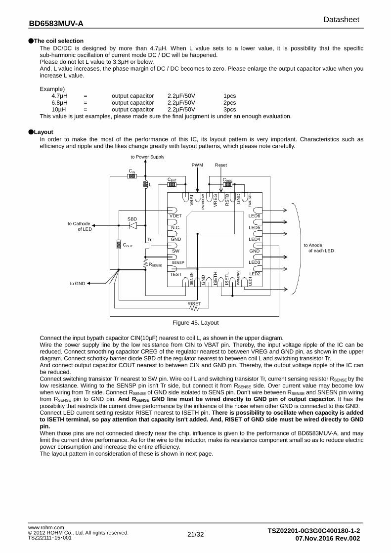
This value is just examples, please made sure the final judgment is under an enough evaluation. Layout
In order to make the most of the performance of this IC, its layout pattern is very important. Characteristics such as efficiency and ripple and the likes change greatly with layout patterns, which please note carefully.
Figure 45. Layout
Connect the input bypath capacitor CIN(10µF) nearest to coil L, as shown in the upper diagram. Wire the power supply line by the low resistance from CIN to VBAT pin. Thereby, the input voltage ripple of the IC can be reduced. Connect smoothing capacitor CREG of the regulator nearest to between VREG and GND pin, as shown in the upper diagram. Connect schottky barrier diode SBD of the regulator nearest to between coil L and switching transistor Tr. And connect output capacitor COUT nearest to between CIN and GND pin. Thereby, the output voltage ripple of the IC can be reduced. Connect switching transistor Tr nearest to SW pin. Wire coil L and switching transistor Tr, current sensing resistor RSENSE by the low resistance. Wiring to the SENSP pin isn't Tr side, but connect it from RSENSE side. Over current value may become low when wiring from Tr side. Connect RSENSE of GND side isolated to SENS pin. Don’t wire between RSENSE and SNESN pin wiring from RSENSE pin to GND pin. And R SENSE GND line must be wired directly to GND pin of outp ut capacitor. It has the possibility that restricts the current drive performance by the influence of the noise when other GND is connected to this GND. Connect LED current setting resistor RISET nearest to ISETH pin. There is possibility to oscillate when capacity is added to ISETH terminal, so pay attention that capacity i sn't added. And, RISET of GND side must be wired dir ectly to GND pin. When those pins are not connected directly near the chip, influence is given to the performance of BD6583MUV-A, and may limit the current drive performance. As for the wire to the inductor, make its resistance component small so as to reduce electric power consumption and increase the entire efficiency. The layout pattern in consideration of these is shown in next page.
LED6
LED5
LED4
LED3
LED2
GND
TEST
GND L ED 6 LE D5 L ED 4 LE D3 LED 2
VDET
N.C.
SW
SENSP
VB
AT
PW
MP
OW
VR
EG
RS
TB
GN
D
FAIL
SE
L
SE
NS
N
GN
D
ISE
TH
ISE
TL
PW
MD
RV
LED
1
PWM Reset
CBAT L
CIN
to Power Supply
Tr
SBD
RSENSE
COUT
to Cathode of LED
CREG
RISET
to Anode of each LED
to GND

Datasheet
22/32
BD6583MUV-A
TSZ02201-0G3G0C400180-1-207.Nov.2016 Rev.002
© 2012 ROHM Co., Ltd. All rights reserved. www.rohm.com
TSZ22111・15・001
Recommended layout pattern
Figure 46. Frontal surface <Top view>
Figure 47. Rear surface <Top view>
COUT CIN
CBAT
L Tr
CREG
RISET
BD6583MUV-A
RSENSE

Datasheet
23/32
BD6583MUV-A
TSZ02201-0G3G0C400180-1-207.Nov.2016 Rev.002
© 2012 ROHM Co., Ltd. All rights reserved. www.rohm.com
TSZ22111・15・001
Selection of external parts Recommended external parts are as shown below. When to use other parts than these, select the following equivalent parts. Coil
Value Manufacturer Product number Size DC current
(mA) DCR (Ω) Vertical Horizontal Height (MAX)
4.7µH TOKO A915AY-4R7M 5.2 5.2 3.0 1870 0.045
4.7µH TOKO B1015AS-4R7M 8.4 8.3 4.0 3300 0.038 4.7µH TOKO A1101AS-4R7M 4.1 4.1 1.2 1400 0.115 4.7µH TDK LTF5022T-4R7N2R0 5.0 5.2 2.2 2000 0.073
4.7µH TDK VLP6810T-4R7M1R6 6.3 6.8 1.0 1600 0.167 10µH TDK VLP6810T-100M1R1 6.3 6.8 1.0 1100 0.350
Capacitor
Value Pressure Manufacturer Product number Size
TC Cap Tolerance Vertical Horizontal Height
[ Supply voltage capacitor ]
10µF 25V MURATA GRM31CB31E106K 3.2 1.6 1.6±0.2 B +/-10% 10µF 10V MURATA GRM219R61A106K 2.0 1.25 0.85±0.15 X5R +/-10% 4.7µF 25V MURATA GRM319R61E475K 3.2 1.6 0.85±0.1 X5R +/-10%
4.7µF 25V MURATA GRM21BR61E475K 2.0 1.25 1.25±0.1 X5R +/-10% [ Smoothing capacitor for built-in regulator ]
1µF 10V MURATA GRM188B10J105K 1.6 0.8 0.8±0.1 B +/-10%
[ Output capacitor ] 1µF 50V MURATA GRM31MB31H105K 3.2 1.6 1.15±0.1 B +/-10% 1µF 50V MURATA GRM21BB31H105K 2.0 1.25 1.25±0.1 B +/-10%
2.2µF 50V MURATA GRM31CB31H225K 3.2 1.6 1.6±0.2 B +/-10% 0.33µF 50V MURATA GRM219B31H334K 2.0 1.25 0.85±0.1 B +/-10%
Resistor
Value Tolerance Manufacturer Product number Size
Vertical Horizontal Height
[ Resistor for LED current decision <ISETH pin> ] 30kΩ ±0.5% ROHM MCR006YZPD3002 0.6 0.3 0.23
[ Resistor for over current decision <SENSP pin> ]
100mΩ ±1% ROHM MCR10EZHFLR100 2.0 1.25 0.55
SBD
Pressure Manufacturer Product number Size
Vertical Horizontal Height 60V ROHM RB160M-60 3.5 1.6 0.8
MOS FET Nch
Pressure Manufacturer Product number Size Current
ability Driving voltage Vertical Horizontal Height
45V ROHM RTR020N05 2.8 2.9 1.0 2A 2.5V 60V ROHM RSH065N06 6.0 5.0 1.75 6.5A 4.0V
The coil is the part that is most influential to efficiency. Select the coil whose direct current resistor (DCR) and current - inductance characteristic is excellent. BD6583MUV-A is designed for the inductance value of 4.7µH. Don’t uses the inductance value less than 2.2µH. Select a capacitor of ceramic type with excellent frequency and temperature characteristics. Further, select Capacitor to be used with small direct current resistance, and pay sufficient attention to the layout pattern shown in Page.21.

Datasheet
24/32
BD6583MUV-A
TSZ02201-0G3G0C400180-1-207.Nov.2016 Rev.002
© 2012 ROHM Co., Ltd. All rights reserved. www.rohm.com
TSZ22111・15・001
Attention point of board layout In board pattern design, the wiring of power supply line should be low Impedance, and put the bypass capacitor if necessary. Especially the wiring impedance must be lower around the DC/DC converter.
About heat loss In heat design, operate the DC/DC converter in the following condition. (The following temperature is a guarantee temperature, so consider the margin.) 1. Periphery temperature Ta must be less than 85
. 2. The loss of IC must be less than dissipation Pd.
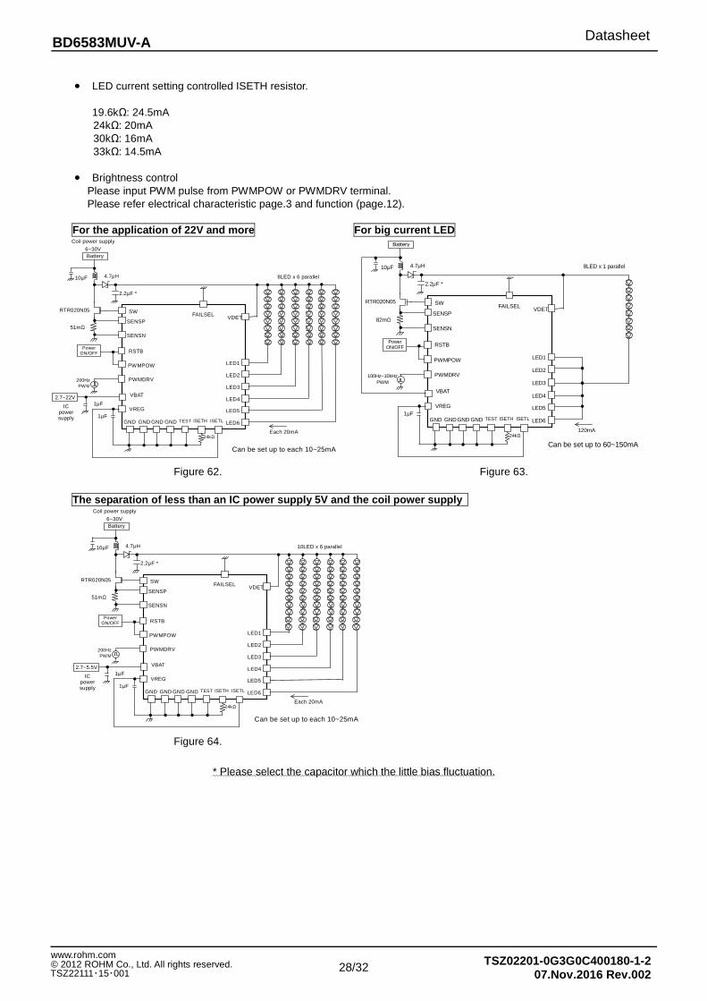
Application example • LED current setting controlled ISETH resistor.
19.6kΩ: 24.5mA 24kΩ: 20mA 30kΩ: 16mA 33kΩ: 14.5mA
• Brightness control
Please input PWM pulse from PWMPOW or PWMDRV terminal. Please refer electrical characteristic p.3 and function (p.12).
15inch panel
10µF
Battery
VDET SW
LED1
LED2
LED3
4.7µH 10LED x 6 parallel
SENSP
SENSN
LED4
Each 20mA
47mΩ
RTR020N05
2.2µF *
RSTB
PWMPOW
PWMDRV
Power ON/OFF
100Hz~10kHz PWM
VBAT
LED5
LED6
FAILSEL
GND
24kΩ
TEST
GND
ISETH
VREG 1µF
ISETL GND
GND
Can be set up to each 10 ~25mA
Figure 48. 10 series×6 parallel, LED current 20mA setting
Current driver PWM application 13 to 14inch panel
10µF
Battery
VDET SW
LED1
LED2
LED3
4.7µH 8LED x 6 parallel
SENSP
SENSN
LED4
Each 20mA
51mΩ
RTR020N05
2.2µF *
RSTB
PWMPOW
PWMDRV
Power
ON/OFF
100Hz~1kHz PWM
VBAT
LED5
LED6
FAILSEL
GND
24kΩ
TEST
GND
ISETH
VREG 1µF
ISETL GND
GND
Can be set up to each 10~25mA
10µF
Battery
VDET SW
LED1
LED2
LED3
4.7µH 8LED x 6 parallel
SENSP
SENSN
LED4
Each 20mA
51mΩ
RTR020N05
2.2µF *
RSTB
PWMPOW
PWMDRV
Power ON/OFF
100Hz~10kHz PWM
VBAT
LED5
LED6
FAILSEL
GND
24kΩ
TEST
GND
ISETH
VREG 1µF
ISETL GND
GND
Can be set up to each 10~25mA
Figure 49. 8 series× parallel, LED current 20mA setting Figure 50. 8 series×6 parallel, LED current 20mA setting
Power control PWM application;:n Current driver PWM application

Datasheet
25/32
BD6583MUV-A
TSZ02201-0G3G0C400180-1-207.Nov.2016 Rev.002
© 2012 ROHM Co., Ltd. All rights reserved. www.rohm.com
TSZ22111・15・001
• LED current setting controlled ISETH resistor.
19.6kΩ: 24.5mA 24kΩ: 20mA 30kΩ: 16mA 33kΩ: 14.5mA
• Brightness control Please input PWM pulse from PWMPOW or PWMDRV terminal. Please refer electrical characteristic page.3 and function (page.12).
10 to 12inch panel
10µF
Battery
VDET SW
LED1
LED2
LED3
4.7µH 7LED x 6 parallel
SENSP
SENSN
LED4
Each 16mA
56mΩ
RTR020N05
2.2µF *
RSTB
PWMPOW
PWMDRV
Power ON/OFF
100Hz~10kHz PWM
VBAT
LED5
LED6
FAILSEL
GND
30kΩ
TEST
GND
ISETH
VREG 1µF
ISETL GND
GND
Can be set up to each 10~25mA
10µF
Battery
VDET SW
LED1
LED2
LED3
4.7µH 10LED x4 parallel
SENSP
SENSN
LED4
Each 20mA
56mΩ
RTR020N05
2.2µF *
RSTB
PWMPOW
PWMDRV
Power ON/OFF
100Hz~10kHz PWM
VBAT
LED5
LED6
FAILSEL
GND
24kΩ
TEST
GND
ISETH
VREG 1µF
ISETL GND
GND
Can be set up to each 10~25mA
Figure 51. 7 series×6 parallel, LED current 16mA setting Figure 52. 10 series×4 parallel, LED current 20mA setting Current driver PWM application Current driver PWM application
7inch panel
10µF
Battery
VDET SW
LED1
LED2
LED3
4.7µH 8LED x 3 parallel
SENSP
SENSN
LED4
Each 20mA
68mΩ
RTR020N05
2.2µF *
RSTB
PWMPOW
PWMDRV
Power ON/OFF
100Hz~10kHz PWM
VBAT
LED5
LED6
FAILSEL
GND
24kΩ
TEST
GND
ISETH
VREG 1µF
ISETL GND
GND
Can be set up to each 10~25mA
10µF
Battery
VDET SW
LED1
LED2
LED3
4.7µH 6LED x 4 parallel
SENSP
SENSN
LED4
Each 20mA
68mΩ
RTR020N05
2.2µF *
RSTB
PWMPOW
PWMDRV
Power ON/OFF
100Hz~10kHz PWM
VBAT
LED5
LED6
FAILSEL
GND
24kΩ
TEST
GND
ISETH
VREG 1µF
ISETL GND
GND
Can be set up to each 10~25mA
Figure 53. 8 series×3 parallel, LED current 20mA setting Figure 54. 6 series×4 parallel, LED current 20mA setting Current driver PWM application Current driver PWM application
* Please select the capacitor which the little bias fluctuation.

Datasheet
26/32
BD6583MUV-A
TSZ02201-0G3G0C400180-1-207.Nov.2016 Rev.002
© 2012 ROHM Co., Ltd. All rights reserved. www.rohm.com
TSZ22111・15・001
• LED current setting controlled ISETH resistor.
19.6kΩ: 24.5mA 24kΩ: 20mA 30kΩ: 16mA 33kΩ: 14.5mA
• Brightness control
Please input PWM pulse from PWMPOW or PWMDRV terminal. Please refer electrical characteristic page.3 and function (page.12).
7inch panel
10µF
Battery
VDET SW
LED1
LED2
LED3
4.7µH 4LED x 6 parallel
SENSP
SENSN
LED4
Each 20mA
68mΩ
RTR020N05
2.2µF *
RSTB
PWMPOW
PWMDRV
Power
ON/OFF
100Hz~1kHz PWM
VBAT
LED5
LED6
FAILSEL
GND
24kΩ
TEST
GND
ISETH
VREG 1µF
ISETL GND
GND
Can be set up to each 10~25mA
10µF
Battery
VDET SW
LED1
LED2
LED3
4.7µH 8LED x 3 parallel
SENSP
SENSN
LED4
Each 40mA
68mΩ
RTR020N05
2.2µF *
RSTB
PWMPOW
PWMDRV
Power ON/OFF
100Hz~1kHz PWM
VBAT
LED5
LED6
FAILSEL
GND
24kΩ
TEST
GND
ISETH
VREG 1µF
ISETL GND
GND
Can be set up to each 20~50mA
Figure 55. 4 series×6 parallel, LED current 20mA setting Figure 56. 8 series×3 parallel, LED current 40mA setting Power control PWM application Power control PWM application
5inch panel
10µF
Battery
VDET SW
LED1
LED2
LED3
4.7µH 8LED x 2 parallel
SENSP
SENSN
LED4
Each 20mA
82mΩ
RTR020N05
2.2µF *
RSTB
PWMPOW
PWMDRV
Power ON/OFF
100Hz~10kHz PWM
VBAT
LED5
LED6
FAILSEL
GND
24kΩ
TEST
GND
ISETH
VREG 1µF
ISETL GND
GND
Can be set up to each 10~25mA
10µF
Battery
VDET SW
LED1
LED2
LED3
4.7µH 8LED x 2 parallel
SENSP
SENSN
LED4
Each 40mA
82mΩ
RTR020N05
2.2µF *
RSTB
PWMPOW
PWMDRV
Power ON/OFF
100Hz~1kHz PWM
VBAT
LED5
LED6
FAILSEL
GND
24kΩ
TEST
GND
ISETH
VREG 1µF
ISETL GND
GND
Can be set up to each 20~50mA
Figure 57. 8 series×2 parallel, LED current 20mA setting Figure 58. 8 series×2 parallel, LED current 40mA setting Current driver PWM application Power control PWM application
* Please select the capacitor which the little bias fluctuation.

Datasheet
27/32
BD6583MUV-A
TSZ02201-0G3G0C400180-1-207.Nov.2016 Rev.002
© 2012 ROHM Co., Ltd. All rights reserved. www.rohm.com
TSZ22111・15・001
• LED current setting controlled ISETH resistor.
19.6kΩ: 24.5mA 24kΩ: 20mA 30kΩ: 16mA 33kΩ: 14.5mA
• Brightness control
Please input PWM pulse from PWMPOW or PWMDRV terminal. Please refer electrical characteristic page.3 and function (page.12).
5inch panel
10µF
Battery
VDET SW
LED1
LED2
LED3
4.7µH 4LED x 4 parallel
SENSP
SENSN
LED4
Each 20mA
82mΩ
RTR020N05
2.2µF *
RSTB
PWMPOW
PWMDRV
Power ON/OFF
100Hz~10kHz PWM
VBAT
LED5
LED6
FAILSEL
GND
24kΩ
TEST
GND
ISETH
VREG 1µF
ISETL GND
GND
Can be set up to each 10~25mA
10µF
Battery
VDET SW
LED1
LED2
LED3
4.7µH 8LED x 2 parallel
SENSP
SENSN
LED4
Each 60mA
82mΩ
RTR020N05
2.2µF *
RSTB
PWMPOW
PWMDRV
Power ON/OFF
100Hz~10kHz PWM
VBAT
LED5
LED6
FAILSEL
GND
24kΩ
TEST
GND
ISETH
VREG 1µF
ISETL GND
GND
Can be set up to each 30~75mA
Figure 59. 4 series×4 parallel, LED current 20mA setting Figure 60. 8 series×2 parallel, LED current 60mA setting Current driver PWM application Current driver PWM application
10µF
Battery
VDET SW
LED1
LED2
LED3
4.7µH 3LED x 5 parallel
SENSP
SENSN
LED4
Each 20mA
82mΩ
RTR020N05
2.2µF *
RSTB
PWMPOW
PWMDRV
Power
ON/OFF
100Hz~1kHz PWM
VBAT
LED5
LED6
FAILSEL
GND
24kΩ
TEST
GND
ISETH
VREG 1µF
ISETL GND
GND
Can be set up to each 10~25mA
Figure 61. 3 series×5 parallel, LED current 20mA setting Power control PWM application
* Please select the capacitor which the little bias fluctuation.
Datasheet
28/32
BD6583MUV-A
TSZ02201-0G3G0C400180-1-207.Nov.2016 Rev.002
© 2012 ROHM Co., Ltd. All rights reserved. www.rohm.com
TSZ22111・15・001
• LED current setting controlled ISETH resistor.
19.6kΩ: 24.5mA 24kΩ: 20mA 30kΩ: 16mA 33kΩ: 14.5mA
• Brightness control Please input PWM pulse from PWMPOW or PWMDRV terminal. Please refer electrical characteristic page.3 and function (page.12).
For the application of 22V and more For big curren t LED
10µF
Battery
VDET SW
LED1
LED2
LED3
4.7µH 8LED x 6 parallel
SENSP
SENSN
LED4
Each 20mA
51mΩ
RTR020N05
2.2µF *
RSTB
PWMPOW
PWMDRV
Power ON/OFF
200HzPWM
VBAT
LED5
LED6
FAILSEL
GND
24kΩ
TEST
GND
ISETH
VREG 1µF
ISETL GND
GND
2.7~22V 1µF
Coil power supply
6~30V
IC power supply
Can be set up to each 10~25mA
10µF
Battery
VDET SW
LED1
LED2
LED3
4.7µH 8LED x 1 parallel
SENSP
SENSN
LED4
120mA
82mΩ
RTR020N05
2.2µF *
RSTB
PWMPOW
PWMDRV
Power ON/OFF
100Hz~10kHz PWM
VBAT
LED5
LED6
FAILSEL
GND
24kΩ
TEST
GND
ISETH
VREG 1µF
ISETL GND
GND
Can be set up to 60~150mA
Figure 62. Figure 63.
The separation of less than an IC power supply 5V a nd the coil power supply
10µF
Battery
VDET SW
LED1
LED2
LED3
4.7µH 10LED x 6 parallel
SENSP
SENSN
LED4
Each 20mA
51mΩ
RTR020N05
2.2µF *
RSTB
PWMPOW
PWMDRV
Power ON/OFF
200HzPWM
VBAT
LED5
LED6
FAILSEL
GND
24kΩ
TEST
GND
ISETH
VREG 1µF
ISETL GND
GND
2.7~5.5V 1µF
Can be set up to each 10~25mA
Coil power supply
6~30V
IC power supply
Figure 64.
* Please select the capacitor which the little bias fluctuation.

Datasheet
29/32
BD6583MUV-A
TSZ02201-0G3G0C400180-1-207.Nov.2016 Rev.002
© 2012 ROHM Co., Ltd. All rights reserved. www.rohm.com
TSZ22111・15・001
Application example of Analog dimming Control LED current to charged D/A voltage. Show application example and typ control.
Please decide final value after you evaluated application, characteristic.
10µF
Battery
VDET SW
LED1
LED2
LED3
4.7µH 8LED x 6 parallel
SENSP
SENSN
LED4
Each 20mA
51mΩ
RTR020N05
2.2µF *
RSTB
PWMPOW
PW MDRV
Power ON/OFF
VBAT
LED5
LED6
FAILSEL
GND
470kΩ
TEST
GND
ISETH
VREG
1µF
ISETL GND
GND
24kΩ
D/A
D/A LED current
0.05V 19.4mA
0.2V 14.4mA
0.4V 7.7mA 0.5V 4.4mA
0.6V 1.0mA 0.7V 0mA
LED current = ISET voltage
470kΩ +
ISET voltage -D/A24kΩ
×800
typ LED current = 0.6V
470kΩ +
0.6V-D/A 24kΩ
×800
Figure 65. Analog style optical application
* Please select the capacitor which the little bias fluctuation.

Datasheet
30/32
BD6583MUV-A
TSZ02201-0G3G0C400180-1-207.Nov.2016 Rev.002
© 2012 ROHM Co., Ltd. All rights reserved. www.rohm.com
TSZ22111・15・001
Operational Notes (1) Absolute Maximum Ratings
An excess in the absolute maximum ratings, such as supply voltage, temperature range of operating conditions, etc., can break down devices, thus making impossible to identify breaking mode such as a short circuit or an open circuit. If any special mode exceeding the absolute maximum ratings is assumed, consideration should be given to take physical safety measures including the use of fuses, etc.
(2) Operating conditions These conditions represent a range within which characteristics can be provided approximately as expected. The electrical characteristics are guaranteed under the conditions of each parameter.
(3) Reverse connection of power supply connector The reverse connection of power supply connector can break down ICs. Take protective measures against the breakdown due to the reverse connection, such as mounting an external diode between the power supply and the IC’s power supply terminal.
(4) Power supply line Design PCB pattern to provide low impedance for the wiring between the power supply and the GND lines. In this regard, for the digital block power supply and the analog block power supply, even though these power supplies has the same level of potential, separate the power supply pattern for the digital block from that for the analog block, thus suppressing the diffraction of digital noises to the analog block power supply resulting from impedance common to the wiring patterns. For the GND line, give consideration to design the patterns in a similar manner. Furthermore, for all power supply terminals to ICs, mount a capacitor between the power supply and the GND terminal. At the same time, in order to use an electrolytic capacitor, thoroughly check to be sure the characteristics of the capacitor to be used present no problem including the occurrence of capacity dropout at a low temperature, thus determining the constant.
(5) GND voltage Make setting of the potential of the GND terminal so that it will be maintained at the minimum in any operating state. Furthermore, check to be sure no terminals are at a potential lower than the GND voltage including an actual electric transient.
(6) Short circuit between terminals and erroneous mounting In order to mount ICs on a set PCB, pay thorough attention to the direction and offset of the ICs. Erroneous mounting can break down the ICs. Furthermore, if a short circuit occurs due to foreign matters entering between terminals or between the terminal and the power supply or the GND terminal, the ICs can break down.
(7) Operation in strong electromagnetic field Be noted that using ICs in the strong electromagnetic field can malfunction them.
(8) Inspection with set PCB On the inspection with the set PCB, if a capacitor is connected to a low-impedance IC terminal, the IC can suffer stress. Therefore, be sure to discharge from the set PCB by each process. Furthermore, in order to mount or dismount the set PCB to/from the jig for the inspection process, be sure to turn OFF the power supply and then mount the set PCB to the jig. After the completion of the inspection, be sure to turn OFF the power supply and then dismount it from the jig. In addition, for protection against static electricity, establish a ground for the assembly process and pay thorough attention to the transportation and the storage of the set PCB.
(9) Input terminals In terms of the construction of IC, parasitic elements are inevitably formed in relation to potential. The operation of the parasitic element can cause interference with circuit operation, thus resulting in a malfunction and then breakdown of the input terminal. Therefore, pay thorough attention not to handle the input terminals, such as to apply to the input terminals a voltage lower than the GND respectively, so that any parasitic element will operate. Furthermore, do not apply a voltage to the input terminals when no power supply voltage is applied to the IC. In addition, even if the power supply voltage is applied, apply to the input terminals a voltage lower than the power supply voltage or within the guaranteed value of electrical characteristics.
(10) Ground wiring pattern If small-signal GND and large-current GND are provided, It will be recommended to separate the large-current GND pattern from the small-signal GND pattern and establish a single ground at the reference point of the set PCB so that resistance to the wiring pattern and voltage fluctuations due to a large current will cause no fluctuations in voltages of the small-signal GND. Pay attention not to cause fluctuations in the GND wiring pattern of external parts as well.
(11) External capacitor In order to use a ceramic capacitor as the external capacitor, determine the constant with consideration given to a degradation in the nominal capacitance due to DC bias and changes in the capacitance due to temperature, etc.
(12) Thermal shutdown circuit (TSD) When junction temperatures become 175°C (typ) or hi gher, the thermal shutdown circuit operates and turns a switch OFF. The thermal shutdown circuit, which is aimed at isolating the LSI from thermal runaway as much as possible, is not aimed at the protection or guarantee of the LSI. Therefore, do not continuously use the LSI with this circuit operating or use the LSI assuming its operation.
(13) Thermal design Perform thermal design in which there are adequate margins by taking into account the permissible dissipation (Pd) in actual states of use.
(14) Selection of coil Select the low DCR inductors to decrease power loss for DC/DC converter.

Datasheet
31/32
BD6583MUV-A
TSZ02201-0G3G0C400180-1-207.Nov.2016 Rev.002
© 2012 ROHM Co., Ltd. All rights reserved. www.rohm.com
TSZ22111・15・001
Ordering Information
B D 6 5 8 3 M U V - A E2
Part Number Package
MUV= VQFN024V4040 Packaging and forming specification
E2: Embossed tape and reel
Marking Diagram Physical Dimension Tape and Reel Information Figure 67. VQFN024V4040
Status of this document The Japanese version of this document is formal specification. A customer may use this translation version only for a reference to help reading the formal version. If there are any differences in translation version of this document formal version takes priority.
(Unit : mm)
VQFN024V4040
0.08 S
S
1 6
7
1219
24
1318
0.4±
0.1
0.02
+0.
03-0
.02
1PIN MARK
2.4±
0.1
C0.2
0.5
4.0±
0.1
0.75
2.4±0.1
4.0±0.1
1.0M
AX
(0.2
2)
0.25+0.05-0.04
∗ Order quantity needs to be multiple of the minimum quantity.
<Tape and Reel information>
Embossed carrier tapeTape
Quantity
Direction of feed
The direction is the 1pin of product is at the upper left when you hold reel on the left hand and you pull out the tape on the right hand
2500pcs
E2
( )
Direction of feed
Reel1pin
Figure 66. Marking Diagram
VQFN024V4040 (TOP VIEW)
D6583
1PIN MARK
Part Number Marking
LOT Number
A
Datasheet
32/32
BD6583MUV-A
TSZ02201-0G3G0C400180-1-207.Nov.2016 Rev.002
© 2012 ROHM Co., Ltd. All rights reserved. www.rohm.com
TSZ22111・15・001
Revision History
Date Revision Changes
03.Dec.2012 001 New Release
07.Nov.2016 002
P.4 Pin ESD Type P.13 Figure. 31 Modification P.18 Figure. 41 Modification P. 31 Figure. 66 Modification

Notice-PGA-E Rev.003
© 2015 ROHM Co., Ltd. All rights reserved.
Notice
Precaution on using ROHM Products 1. Our Products are designed and manufactured for application in ordinary electronic equipments (such as AV equipment,
OA equipment, telecommunication equipment, home electronic appliances, amusement equipment, etc.). If you intend to use our Products in devices requiring extremely high reliability (such as medical equipment
(Note 1), transport
equipment, traffic equipment, aircraft/spacecraft, nuclear power controllers, fuel controllers, car equipment including car accessories, safety devices, etc.) and whose malfunction or failure may cause loss of human life, bodily injury or serious damage to property (“Specific Applications”), please consult with the ROHM sales representative in advance. Unless otherwise agreed in writing by ROHM in advance, ROHM shall not be in any way responsible or liable for any damages, expenses or losses incurred by you or third parties arising from the use of any ROHM’s Products for Specific Applications.
(Note1) Medical Equipment Classification of the Specific Applications
JAPAN USA EU CHINA
CLASSⅢ CLASSⅢ
CLASSⅡb CLASSⅢ
CLASSⅣ CLASSⅢ
2. ROHM designs and manufactures its Products subject to strict quality control system. However, semiconductor
products can fail or malfunction at a certain rate. Please be sure to implement, at your own responsibilities, adequate safety measures including but not limited to fail-safe design against the physical injury, damage to any property, which a failure or malfunction of our Products may cause. The following are examples of safety measures:
[a] Installation of protection circuits or other protective devices to improve system safety [b] Installation of redundant circuits to reduce the impact of single or multiple circuit failure
3. Our Products are designed and manufactured for use under standard conditions and not under any special or extraordinary environments or conditions, as exemplified below. Accordingly, ROHM shall not be in any way responsible or liable for any damages, expenses or losses arising from the use of any ROHM’s Products under any special or extraordinary environments or conditions. If you intend to use our Products under any special or extraordinary environments or conditions (as exemplified below), your independent verification and confirmation of product performance, reliability, etc, prior to use, must be necessary:
[a] Use of our Products in any types of liquid, including water, oils, chemicals, and organic solvents [b] Use of our Products outdoors or in places where the Products are exposed to direct sunlight or dust [c] Use of our Products in places where the Products are exposed to sea wind or corrosive gases, including Cl2,
H2S, NH3, SO2, and NO2
[d] Use of our Products in places where the Products are exposed to static electricity or electromagnetic waves [e] Use of our Products in proximity to heat-producing components, plastic cords, or other flammable items [f] Sealing or coating our Products with resin or other coating materials [g] Use of our Products without cleaning residue of flux (even if you use no-clean type fluxes, cleaning residue of
flux is recommended); or Washing our Products by using water or water-soluble cleaning agents for cleaning residue after soldering
[h] Use of the Products in places subject to dew condensation
4. The Products are not subject to radiation-proof design. 5. Please verify and confirm characteristics of the final or mounted products in using the Products. 6. In particular, if a transient load (a large amount of load applied in a short period of time, such as pulse. is applied,
confirmation of performance characteristics after on-board mounting is strongly recommended. Avoid applying power exceeding normal rated power; exceeding the power rating under steady-state loading condition may negatively affect product performance and reliability.
7. De-rate Power Dissipation depending on ambient temperature. When used in sealed area, confirm that it is the use in
the range that does not exceed the maximum junction temperature. 8. Confirm that operation temperature is within the specified range described in the product specification. 9. ROHM shall not be in any way responsible or liable for failure induced under deviant condition from what is defined in
this document.
Precaution for Mounting / Circuit board design 1. When a highly active halogenous (chlorine, bromine, etc.) flux is used, the residue of flux may negatively affect product
performance and reliability.
2. In principle, the reflow soldering method must be used on a surface-mount products, the flow soldering method must be used on a through hole mount products. If the flow soldering method is preferred on a surface-mount products, please consult with the ROHM representative in advance.
For details, please refer to ROHM Mounting specification

Notice-PGA-E Rev.003
© 2015 ROHM Co., Ltd. All rights reserved.
Precautions Regarding Application Examples and External Circuits 1. If change is made to the constant of an external circuit, please allow a sufficient margin considering variations of the
characteristics of the Products and external components, including transient characteristics, as well as static characteristics.
2. You agree that application notes, reference designs, and associated data and information contained in this document
are presented only as guidance for Products use. Therefore, in case you use such information, you are solely responsible for it and you must exercise your own independent verification and judgment in the use of such information contained in this document. ROHM shall not be in any way responsible or liable for any damages, expenses or losses incurred by you or third parties arising from the use of such information.
Precaution for Electrostatic This Product is electrostatic sensitive product, which may be damaged due to electrostatic discharge. Please take proper caution in your manufacturing process and storage so that voltage exceeding the Products maximum rating will not be applied to Products. Please take special care under dry condition (e.g. Grounding of human body / equipment / solder iron, isolation from charged objects, setting of Ionizer, friction prevention and temperature / humidity control).
Precaution for Storage / Transportation 1. Product performance and soldered connections may deteriorate if the Products are stored in the places where:
[a] the Products are exposed to sea winds or corrosive gases, including Cl2, H2S, NH3, SO2, and NO2 [b] the temperature or humidity exceeds those recommended by ROHM [c] the Products are exposed to direct sunshine or condensation [d] the Products are exposed to high Electrostatic
2. Even under ROHM recommended storage condition, solderability of products out of recommended storage time period may be degraded. It is strongly recommended to confirm solderability before using Products of which storage time is exceeding the recommended storage time period.
3. Store / transport cartons in the correct direction, which is indicated on a carton with a symbol. Otherwise bent leads
may occur due to excessive stress applied when dropping of a carton. 4. Use Products within the specified time after opening a humidity barrier bag. Baking is required before using Products of
which storage time is exceeding the recommended storage time period.
Precaution for Product Label A two-dimensional barcode printed on ROHM Products label is for ROHM’s internal use only.
Precaution for Disposition When disposing Products please dispose them properly using an authorized industry waste company.
Precaution for Foreign Exchange and Foreign Trade act Since concerned goods might be fallen under listed items of export control prescribed by Foreign exchange and Foreign trade act, please consult with ROHM in case of export.
Precaution Regarding Intellectual Property Rights 1. All information and data including but not limited to application example contained in this document is for reference
only. ROHM does not warrant that foregoing information or data will not infringe any intellectual property rights or any other rights of any third party regarding such information or data.
2. ROHM shall not have any obligations where the claims, actions or demands arising from the combination of the Products with other articles such as components, circuits, systems or external equipment (including software).
3. No license, expressly or implied, is granted hereby under any intellectual property rights or other rights of ROHM or any third parties with respect to the Products or the information contained in this document. Provided, however, that ROHM will not assert its intellectual property rights or other rights against you or your customers to the extent necessary to manufacture or sell products containing the Products, subject to the terms and conditions herein.
Other Precaution 1. This document may not be reprinted or reproduced, in whole or in part, without prior written consent of ROHM.
2. The Products may not be disassembled, converted, modified, reproduced or otherwise changed without prior written consent of ROHM.
3. In no event shall you use in any way whatsoever the Products and the related technical information contained in the Products or this document for any military purposes, including but not limited to, the development of mass-destruction weapons.
4. The proper names of companies or products described in this document are trademarks or registered trademarks of ROHM, its affiliated companies or third parties.

DatasheetDatasheet
Notice – WE Rev.001© 2015 ROHM Co., Ltd. All rights reserved.
General Precaution 1. Before you use our Pro ducts, you are requested to care fully read this document and fully understand its contents.
ROHM shall n ot be in an y way responsible or liabl e for fa ilure, malfunction or acci dent arising from the use of a ny ROHM’s Products against warning, caution or note contained in this document.
2. All information contained in this docume nt is current as of the issuing date and subj ect to change without any prior
notice. Before purchasing or using ROHM’s Products, please confirm the la test information with a ROHM sale s representative.
3. The information contained in this doc ument is provi ded on an “as is” basis and ROHM does not warrant that all
information contained in this document is accurate an d/or error-free. ROHM shall not be in an y way responsible or liable for any damages, expenses or losses incurred by you or third parties resulting from inaccuracy or errors of or concerning such information.