
5.8. Common-collector amplifier. - Texas A&M Universityece.tamu.edu/~spalermo/ecen325/Chapter...
26
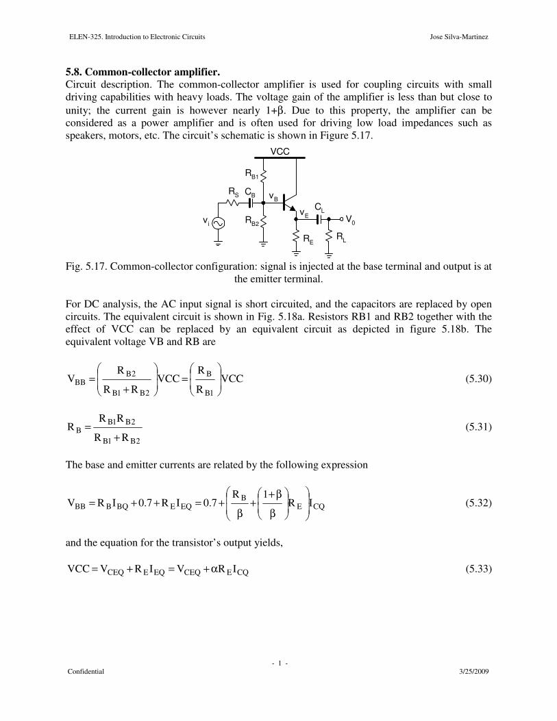
ELEN-325. Introduction to Electronic Circuits Jose Silva-Martinez - 1 - Confidential 3/25/2009 5.8. Common-collector amplifier. Circuit description. The common-collector amplifier is used for coupling circuits with small driving capabilities with heavy loads. The voltage gain of the amplifier is less than but close to unity; the current gain is however nearly 1+β. Due to this property, the amplifier can be considered as a power amplifier and is often used for driving low load impedances such as speakers, motors, etc. The circuit’s schematic is shown in Figure 5.17. VCC v i v E R B1 R B2 v B R E C B R S R L V 0 C L Fig. 5.17. Common-collector configuration: signal is injected at the base terminal and output is at the emitter terminal. For DC analysis, the AC input signal is short circuited, and the capacitors are replaced by open circuits. The equivalent circuit is shown in Fig. 5.18a. Resistors RB1 and RB2 together with the effect of VCC can be replaced by an equivalent circuit as depicted in figure 5.18b. The equivalent voltage VB and RB are VCC R R VCC R R R V 1 B B 2 B 1 B 2 B BB = + = (5.30) 2 B 1 B 2 B 1 B B R R R R R + = (5.31) The base and emitter currents are related by the following expression CQ E B EQ E BQ B BB I R 1 R 7 . 0 I R 7 . 0 I R V β β + + β + = + + = (5.32) and the equation for the transistor’s output yields, CQ E CEQ EQ E CEQ I R V I R V VCC α + = + = (5.33)
Transcript of 5.8. Common-collector amplifier. - Texas A&M Universityece.tamu.edu/~spalermo/ecen325/Chapter...
ELEN-325. Introduction to Electronic Circuits Jose Silva-Martinez
- 1 - Confidential 3/25/2009
5.8. Common-collector amplifier. Circuit description. The common-collector amplifier is used for coupling circuits with small driving capabilities with heavy loads. The voltage gain of the amplifier is less than but close to unity; the current gain is however nearly 1+β. Due to this property, the amplifier can be considered as a power amplifier and is often used for driving low load impedances such as speakers, motors, etc. The circuit’s schematic is shown in Figure 5.17.
VCC
vi
vE
RB1
RB2
vB
RE
CBRS
RL
V0
CL
Fig. 5.17. Common-collector configuration: signal is injected at the base terminal and output is at
the emitter terminal. For DC analysis, the AC input signal is short circuited, and the capacitors are replaced by open circuits. The equivalent circuit is shown in Fig. 5.18a. Resistors RB1 and RB2 together with the effect of VCC can be replaced by an equivalent circuit as depicted in figure 5.18b. The equivalent voltage VB and RB are
VCCR
RVCC
RR
RV
1B
B
2B1B
2BBB
=
+= (5.30)
2B1B
2B1BB
RR
RRR
+= (5.31)
The base and emitter currents are related by the following expression
CQEB
EQEBQBBB IR1R
7.0IR7.0IRV
β
β++
β+=++= (5.32)
and the equation for the transistor’s output yields,
CQECEQEQECEQ IRVIRVVCC α+=+= (5.33)
ELEN-325. Introduction to Electronic Circuits Jose Silva-Martinez
- 2 - Confidential 3/25/2009
VCC
RB1
RB2
vB
RE
ICQIBQ
VCC
VCEQRB
RE
ICQIBQ
IEQ
VBB
+
-
+
-
(a) (b)
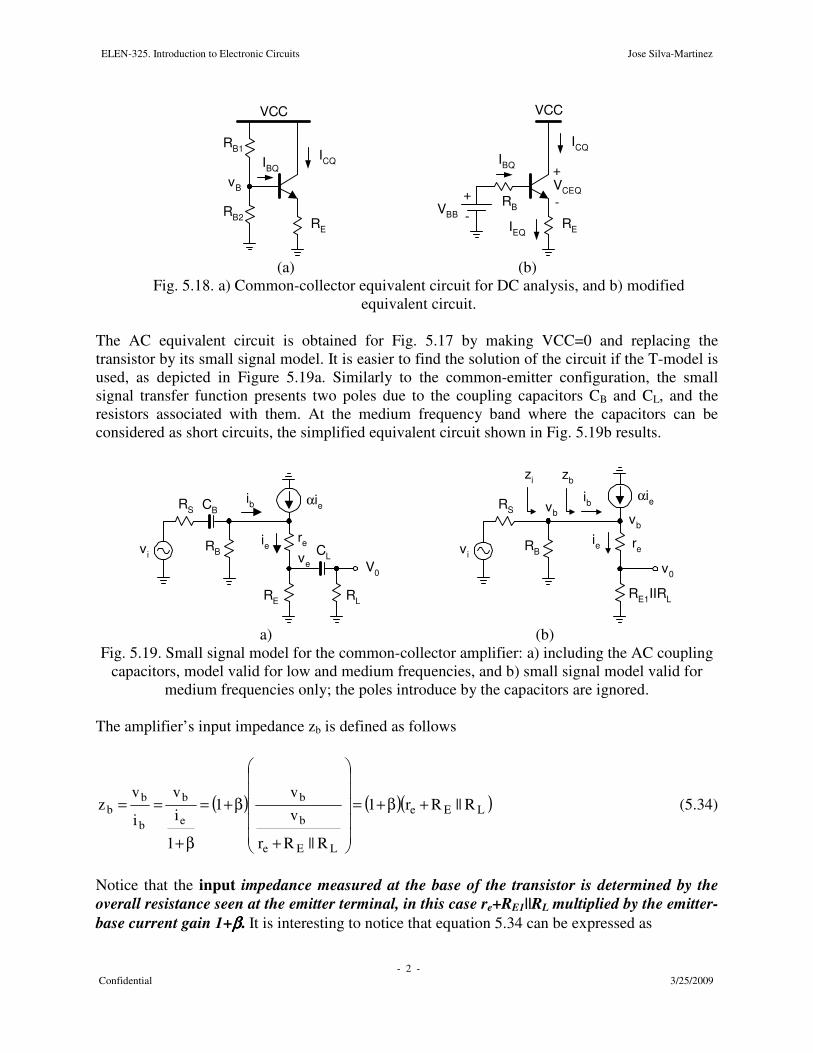
Fig. 5.18. a) Common-collector equivalent circuit for DC analysis, and b) modified equivalent circuit.
The AC equivalent circuit is obtained for Fig. 5.17 by making VCC=0 and replacing the transistor by its small signal model. It is easier to find the solution of the circuit if the T-model is used, as depicted in Figure 5.19a. Similarly to the common-emitter configuration, the small signal transfer function presents two poles due to the coupling capacitors CB and CL, and the resistors associated with them. At the medium frequency band where the capacitors can be considered as short circuits, the simplified equivalent circuit shown in Fig. 5.19b results.
vi ve
RB
RE
CBRS
RL
V0
CL
reie
αieib
viRB
RE1IIRL
RS
v0
reie
αieibvb
zbzi
vb
a) (b)
Fig. 5.19. Small signal model for the common-collector amplifier: a) including the AC coupling capacitors, model valid for low and medium frequencies, and b) small signal model valid for
medium frequencies only; the poles introduce by the capacitors are ignored.
The amplifier’s input impedance zb is defined as follows
( ) ( )( )LEe
LEe
b
b
e
b
b
bb R||Rr1
R||Rr
vv
1
1
iv
i
vz +β+=
+
β+=
β+
== (5.34)
Notice that the input impedance measured at the base of the transistor is determined by the overall resistance seen at the emitter terminal, in this case re+RE1||RL multiplied by the emitter-base current gain 1+ββββ. It is interesting to notice that equation 5.34 can be expressed as

ELEN-325. Introduction to Electronic Circuits Jose Silva-Martinez
- 3 - Confidential 3/25/2009
( )( )LEb R||R1rz β++= π (5.34b) This is an important property of circuits with emitter resistance: the resistors attached at the emitter terminal increase the input impedance seen at the base terminal by a factor (1+β)(RE1||RL). The overall input impedance seen by the input voltage source vi is then
( )( )( )LEBbBi R||R1r||Rz||Rz β++== π (5.35) The voltage vb is generated from the input voltage and the voltage divider due to RS, RB and zb as
iS
i
i
b
zR
z
v
v
+= (5.36)
To avoid signal attenuation at the input stage, it is desirable to design the circuit such that RS << zi=zb||RB. As aforementioned, the impedances connected at the emitter help us to this end. From fig. 5.19, it can be noticed that the output voltage is generated from vb as follows:
LEe
LE
b
o
R||Rr
R||R
v
v
+= (5.37)
By using equations 5.35 and 5.36, the overall voltage gain can be obtained as
+
+=
=
LEe
LE
BbS
Bb
b
o
i
b
i
o
R||Rr
R||R
R||zR
R||z
v
v
v
v
v
v (5.38)
The amplifier’s voltage gain is less than unity, and it is composed by the multiplication of two attenuation factors: the input and output attenuators. The effect of the input voltage source impedance RS is to reduce the overall transfer function, and its effect is minimized if the input impedance of the amplifier is much larger then RS. As a rule of thumb, the attenuation factor is minimized if the conditions zb||RB >> RS and RE1||RL >>re=Vth/IEQ are satisfied. While to satisfy the former condition is relatively easy in most of the practical designs, this is not the case for the latter one since RL could be very small; for instance 8 for many speakers. For an emitter resistance re (=0.025/ IEQ) equal to 8 an emitter current of 3.125 mA. Under these conditions, equation 5.38 leads to an overall voltage gain of less than 0.5. What current is needed if a voltage gain of 0.9 is required? The emitter resistance re must be equal to 0.8 leading to an emitter current of roughly 31 mA. What about driving a 4 speaker? The fundamental equations for the common-collector structure are: 5.30-5.32 for the DC analysis, and 5.35 and 5.38 for the AC behavior. It is left to the reader to demonstrate that the current gain of this topology is close to ββββAC if the amplifier is properly designed; hence the power gain might be close to ββββAC as well. 5.9. Common-base amplifier.
ELEN-325. Introduction to Electronic Circuits Jose Silva-Martinez
- 4 - Confidential 3/25/2009
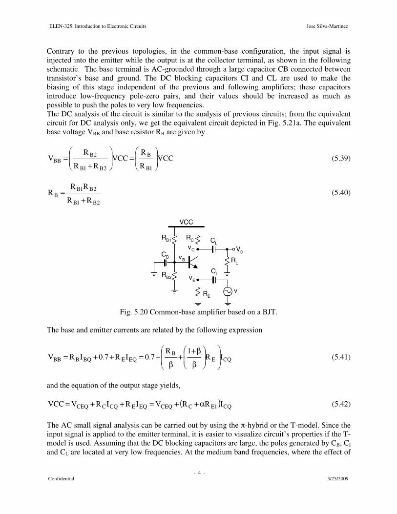
Contrary to the previous topologies, in the common-base configuration, the input signal is injected into the emitter while the output is at the collector terminal, as shown in the following schematic. The base terminal is AC-grounded through a large capacitor CB connected between transistor’s base and ground. The DC blocking capacitors CI and CL are used to make the biasing of this stage independent of the previous and following amplifiers; these capacitors introduce low-frequency pole-zero pairs, and their values should be increased as much as possible to push the poles to very low frequencies. The DC analysis of the circuit is similar to the analysis of previous circuits; from the equivalent circuit for DC analysis only, we get the equivalent circuit depicted in Fig. 5.21a. The equivalent base voltage VBB and base resistor RB are given by
VCCR
RVCC
RR
RV
1B
B
2B1B
2BBB
=
+= (5.39)
2B1B
2B1BB
RR
RRR
+= (5.40)
VCC
vi
vE
RB1
RB2
vB
RE
CB RL
CLRC
V0
CI
vC
Fig. 5.20 Common-base amplifier based on a BJT.
The base and emitter currents are related by the following expression
CQEB
EQEBQBBB IR1R
7.0IR7.0IRV
β
β++
β+=++= (5.41)
and the equation of the output stage yields,
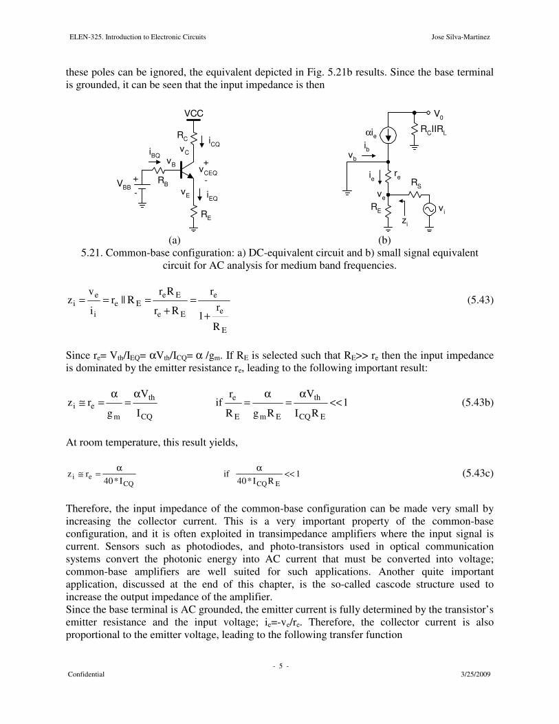
( ) CQ1ECCEQEQECQCCEQ IRRVIRIRVVCC α++=++= (5.42) The AC small signal analysis can be carried out by using the π-hybrid or the T-model. Since the input signal is applied to the emitter terminal, it is easier to visualize circuit’s properties if the T-model is used. Assuming that the DC blocking capacitors are large, the poles generated by CB, CI and CL are located at very low frequencies. At the medium band frequencies, where the effect of
ELEN-325. Introduction to Electronic Circuits Jose Silva-Martinez
- 5 - Confidential 3/25/2009
these poles can be ignored, the equivalent depicted in Fig. 5.21b results. Since the base terminal is grounded, it can be seen that the input impedance is then
VCC
vE
RB
vB
RE
RC
vC
VBB+
-
vCEQ
+
-
iCQiBQ
iEQ
viRE
reie
αieib
vb
RCIIRL
V0
zi
RSve
(a) (b)
5.21. Common-base configuration: a) DC-equivalent circuit and b) small signal equivalent circuit for AC analysis for medium band frequencies.
E
e
e
Ee
EeEe
i
ei
R
r1
r
Rr
RrR||r
i
vz
+=
+=== (5.43)
Since re= Vth/IEQ= αVth/ICQ= α /gm. If RE is selected such that RE>> re then the input impedance is dominated by the emitter resistance re, leading to the following important result:
1RI
V
RgR
rif
I
V
grz
ECQ
th
EmE
e
CQ
th
mei <<
α=
α=
α=
α=≅ (5.43b)
At room temperature, this result yields,
1RI*40
ifI*40
rzECQCQ
ei <<αα=≅ (5.43c)
Therefore, the input impedance of the common-base configuration can be made very small by increasing the collector current. This is a very important property of the common-base configuration, and it is often exploited in transimpedance amplifiers where the input signal is current. Sensors such as photodiodes, and photo-transistors used in optical communication systems convert the photonic energy into AC current that must be converted into voltage; common-base amplifiers are well suited for such applications. Another quite important application, discussed at the end of this chapter, is the so-called cascode structure used to increase the output impedance of the amplifier. Since the base terminal is AC grounded, the emitter current is fully determined by the transistor’s emitter resistance and the input voltage; ie=-ve/re. Therefore, the collector current is also proportional to the emitter voltage, leading to the following transfer function
ELEN-325. Introduction to Electronic Circuits Jose Silva-Martinez
- 6 - Confidential 3/25/2009
( ) ( )e
LCLC
e
eLC
e
c
b
o
rR||R
R||Rv
iR||R
vi
vv
=
α−=
−= (5.44)
The emitter resistance is determined by the DC emitter current and the thermal voltage, hence equation 5.43 can be simplified as
( ) ( ) ( ) mLCm
LCth
EQLC
e
o gR||Rg
R||RV
IR||R
vv
≅
α== (5.44b)
Notice that this equation is similar to that of the common-emitter transistor; the main difference of the two structures is the input impedance: usually the input impedance of the common-emitter configuration is large, especially if an additional resistor is added to the emitter terminal. The common-base configuration presents very small input impedance that makes it a very attractive solution for current-mode sensors such as photo-detectors. The overall voltage gain taking into account the resistance of the input voltage source is obtained from Fig. 5.21b and equation 5.44 as
+=
e
LC
iS
i
i
o
r
R||R
zR
z
v
v (5.45)
The fundamental equations for the 3 topologies are summarized in the following table. Parameter Common-emitter
Fig. 5.22 part Va Common-Collector
Fig. 5.17 Common-Base
Fig. 5.20 DC Equations
( )
+
α+
β+= 2E1E
BCQBB RR
1RI7.0V
α
+++= 2E1E
CCQCEQRR
RIVVCC
CQ1EB
BB IR1R
7.0V
β
β++
β+=
CQ1ECEQ IRVVCC α+= CQE
BBB IR
1R7.0V
β
β++
β+=
CQE
CCEQ IR
RVVCC
++=α
1
Input impedance
( )( ) B1Ei R||R1rz β++= π ( )( )( ) BLEi R||R||R1rz β++= π Eei R||rz =
Voltage gain ( )
+
α
+−=
1Ee
LC
iS
iV
Rr
RR
zR
zA
+
+=
LEe
LE
BiS
Bi
i
o
R||Rr
R||R
R||zR
R||z
v
v
+=
e
LC
iS
i
i
o
r
R||R
zR
z
v
v
Table 5.1 Fundamental equations for the common-emitter, common-collector and common-base configurations.
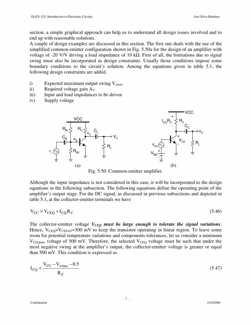
5.10. Amplifier’s design considerations using bipolar devices. Design of a large gain amplifier using a common-emitter structure with limited input impedance: A graphical approach. A major concern of the analog circuit designer is what should be the acceptable range of values for a set of given specifications? This part of the design is obscure in most of the existing literature, and that is the reason why novel designers think that analog design is a kind of black art. In fact the selecting a proper operating point is not a trivial task, since there are many parameters and constraints involved. However, as shown in this
ELEN-325. Introduction to Electronic Circuits Jose Silva-Martinez
- 7 - Confidential 3/25/2009
section, a simple graphical approach can help us to understand all design issues involved and to end up with reasonable solutions. A couple of design examples are discussed in this section. The first one deals with the use of the simplified common-emitter configuration shown in Fig. 5.50a for the design of an amplifier with voltage of -20 V/V driving a load impedance of 10 k. First of all, the limitations due to signal swing must also be incorporated as design constraints. Usually those conditions impose some boundary conditions to the circuit’s solution. Among the equations given in table 5.1, the following design constraints are added. i) Expected maximum output swing Vomax ii) Required voltage gain AV iii) Input and load impedances to be driven iv) Supply voltage
VCC
RCvC
RB1
RB2
vBCB
RL
V0
CL
vi
VCC
vbe
RC
v0
VCE
CC
RL
+
-
ICQRC
+
-
+
-VBB
(a) (b)
Fig. 5.50. Common-emitter amplifier. Although the input impedance is not considered in this case, it will be incorporated to the design equations in the following subsection. The following equations define the operating point of the amplifier’s output stage. For the DC signal, as discussed in previous subsections and depicted in table 5.1, at the collector-emitter terminals we have
CCQCEQCC RIVV += (5.46) The collector-emitter voltage VCEQ must be large enough to tolerate the signal variations. Hence, VCEQ>VCESAT=300 mV to keep the transistor operating in linear region. To leave some room for potential temperature variations and components tolerances, let us consider a minimum VCEQmin voltage of 500 mV. Therefore, the selected VCEQ voltage must be such that under the most negative swing at the amplifier’s output, the collector-emitter voltage is greater or equal than 500 mV. This condition is expressed as
C
maxoCCCQ
R
5.0VVI
−−< (5.47)
ELEN-325. Introduction to Electronic Circuits Jose Silva-Martinez
- 8 - Confidential 3/25/2009
On the other hand, VCEQ can not be close to VCC otherwise we do not have room for the positive signal swing. The voltage drop across the collector resistor RC (ICQRC) must be greater than Vomax, leading to the following bound for the collector current
C
maxoCQ
R
VI > (5.48)
Another important parameter is the small signal voltage gain from transistor’s base to amplifier’s output. From our previous analysis, the voltage gain is given by
( ) ( )th
LCCQLCm
be
0V
V
RRIRRg
v
vA === (5.49a)
or
( )
+=
LC
LCthVCQ
RR
RRVAI (5.49b)
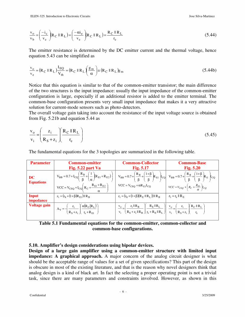
These equations can be plot in the IC-RC plane as shown in the following figure. Equations 5.47 and 5.48 represent the boundaries for the acceptable solutions, and 5.49b is the actual solution for the amplifier’s voltage gain. These plots are function of the required voltage gain Av and the load impedance RL. In Figure 5.51, equation 5.49b is plotted for 4 different amplifier’s gain (AV
= -10, -20, -40 and -100). Notice that the solution’s boundaries (equations 5.47 and 5.48) are independent of the desired voltage gain; these equations however are determined by the maximum voltage swing expected at the amplifier’s output. The results shown in the figure below are generated by using VCC= 5V, Vomax=1 Vpeak and Vth=26 mV and RL=10K.
1E+3 1E+4 1E+5
Rc (Ohms)
0.01
0.10
1.00
10.00
Ic(m
A)
Fig. 5.51. IC-RC plane shown acceptable region.
AV=-100
=-40 =-20 =-10
Acceptable resistance Acceptable current
Eqn 5.49b (AV=-20)
Eqn 5.47
Eqn 5.48

ELEN-325. Introduction to Electronic Circuits Jose Silva-Martinez
- 9 - Confidential 3/25/2009
Notice in this plot that the acceptable region is quite limited for large voltage gains. According to these results it is clear that we can not design a voltage amplifier with gain of –100 for the given supply voltage and the desired output voltage swing. The solution for equation 5.49b does not intersect the acceptable region. For the case of an amplifier with voltage gain of -20, for instance, we can achieve the specifications (all design constraints are satisfied) if and only if the collector resistance is in the range of 9.5kΩ till 58 kΩ. The quiescent collector current must be in the range of 60µA-100µA. Another advantage of using this approach is that the power consumption can be easily optimized by selecting the largest possible collector resistor RC. For practical applications, however, it is always good practice to overdesign the amplifier in order to accommodate both temperature variations and tolerances of the devices and components used. Once the output stage of the circuit is defined and the collector current determined, the base current can be computed. For amplifiers built using discrete components, there is a complete family of devices that can be used. The resistors attached to the base terminal can be computed based on the amount of base current needed and the input impedance required. There are two basic equations (see table 5.1, common-emitter configuration with RE1=RE2=0) and two unknowns; hence we do not have any degree of freedom for optimization. These equations are repeated here for sake of completeness. From the DC analysis we have:
7.0RIVCCR
RBB
1
B +=
(5.50)
and the amplifier’s input impedance (AC analysis) is given by:
BB
B
BBin
R
r1
r
R
r1
r
Rr
RrRrZ
π
π
π
π
π
ππ
+=
+=
+== (5.51)
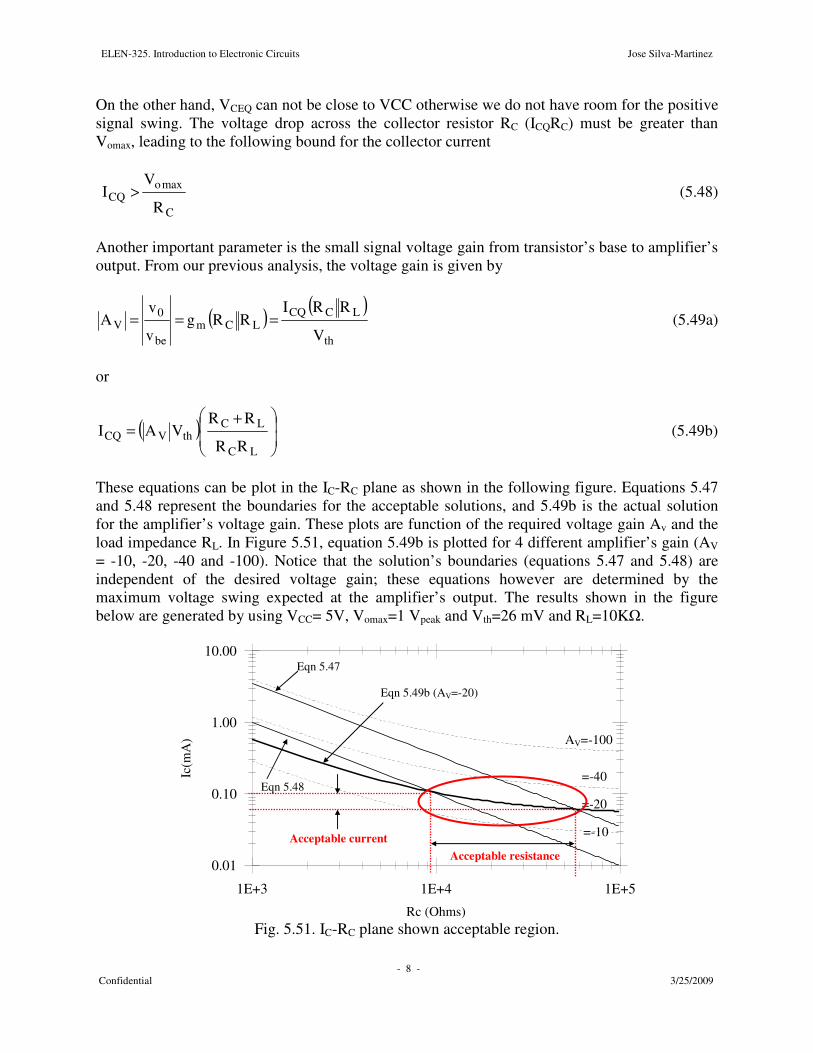
If RB>>rπ, the effect of the bias network becomes negligible on the input impedance, and it is dominated by the transistor’s base-emitter resistance rπ. For practical applications it is common practice to increase as much as possible the input impedance. Thus, selecting a high-beta transistor helps. Large β reduces the base current and increases the input impedance of the amplifier (rπ=Vth/IBQ) but in most of the cases high-β devices have limited current capabilities, and are used as preamplifiers. Typically the transistors used as power amplifiers have limited β; e.g. less than 50. Also, if we select the least possible collector current, the required base current reduces and that increases the input impedance and the power consumption reduces as well. Numerical example. For a gain amplifier of –20 V/V and Vomax=1 Vpk, from figure 5.51, we select IC=80 µA and RC=12 kΩ. For this collector current, the beta of the 2N2222 is close to 150, therefore the DC base current is around 0.8 µA. The base-emitter resistance rπ is around 47 kΩ. Therefore RB can be selected around 300 kΩ and the overall input impedance is around 40 kΩ. Let us use for this exmple RB=400 kΩ; then VB=0.6+IBRB=0.82 V. Since the base current is very small, for our hand calculations we use VBE=0.6 V rather than 0.7 V; anyway, the base-emiter voltage must be obtained from SPICE results, and the resistors should be adjusted accordingly. After some basic algebra, the value of the resistors lumped to the base terminal are
ELEN-325. Introduction to Electronic Circuits Jose Silva-Martinez
- 10 - Confidential 3/25/2009
determined as RB1=2.2 MΩ, and RB2=490kΩ, respectively. Spice waveform at the transistor’s collector is shown below.
Fig. 5.52. Signal waveform at the collector terminal of the BJT. The input signal is 5 mVpk and the voltage gain is 23.5 V/V.
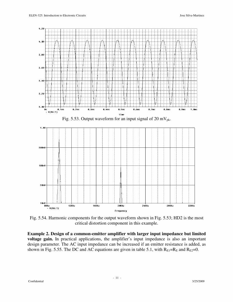
The voltage gain is 15 % larger than the expected one; analyzing the Spice output file we found that the β-ac is 15 % larger than the value used for our hand-calculations. As a result, the DC collector current is also 15% larger, which is evident in Fig. 5.52 analyzing the DC voltage component (average); it is around 3.7 V instead of the expected 4 V (=VCC-12kΩ*80 µA). If needed, using the β obtained from the Spice output file, the base current and resistors lumped to the base can be re-calculated. Although large volatge gain can be obtained with the previous topology, the input signal must be limited to 10 mV, otherwise the small signal approximations are no longer valid. There are two main limitations with this topology: a) the input signal appears directly across the base-emitter terminals, limiting the amplitude of the input signals for linear operation and b) the input impedance is determined by the base-emitter resistance which is not very high. A 20 mV input signal was applied to the previous circuit; the spice results are shown in figure 5.53 and 5.54. Notice that the ouput waveform is not even close to a sinusoidal output. A fourier analysis of this waveform, carried out using the transient simulation option available in Spice, reveals that the fundamental component has an amplitude of roughly 500 mV while the second harmonic component is 80 mV. The second harmonic distortion is rougly 16%, that is not small enough for most practical applications; equation 5.10 predicts HD2 ≈ 20%, which is relativelty close to Spice results. The third harmonic component is 10 mV, leading to a HD3=2%, same value is predicted by equation 5.10.
ELEN-325. Introduction to Electronic Circuits Jose Silva-Martinez
- 11 - Confidential 3/25/2009
Fig. 5.53. Output waveform for an input signal of 20 mVpk.
Fig. 5.54. Harmonic components for the output waveform shown in Fig. 5.53; HD2 is the most
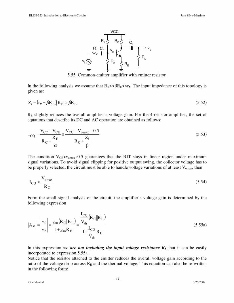
critical distortion component in this example. Example 2. Design of a common-emitter amplifier with larger input impedance but limited voltage gain. In practical applications, the amplifier’s input impedance is also an important design parameter. The AC input impedance can be increased if an emitter resistance is added, as shown in Fig. 5.55. The DC and AC equations are given in table 5.1, with RE1=RE and RE2=0.
ELEN-325. Introduction to Electronic Circuits Jose Silva-Martinez
- 12 - Confidential 3/25/2009
VCC
RC
vi
R1
R2
vb
RE
CBRS
RL
v0
CL
5.55. Common-emitter amplifier with emitter resistor.
In the following analysis we assume that RB>>βRE>>rπ. The input impedance of this topology is given as:
( ) EBEi RRRrZ ββπ ≅+= (5.52) RB slightly reduces the overall amplifier’s voltage gain. For the 4-resistor amplifier, the set of equations that describe its DC and AC operation are obtained as follows:
β+
−−≤
α+
−=
iC
maxoCC
EC
CECCCQ Z
R
5.0VVR
R
VVI (5.53)
The condition VCE>vomax+0.5 guarantees that the BJT stays in linear region under maximum signal variations. To avoid signal clipping for positive output swing, the collector voltage has to be properly selected; the circuit must be able to handle voltage variations of at least Vomax, then
C
maxoCQ
R
VI > (5.54)
Form the small signal analysis of the circuit, the amplifier’s voltage gain is determined by the following expression
( ) ( )
Eth
CQ
LCth
CQ
Em
LCm
b
0V
RV
I1
RRV
I
Rg1
RRg
v
vA
+=
+== (5.55a)
In this expression we are not including the input voltage resistance RS, but it can be easily incorporated to expression 5.55a. Notice that the resistor attached to the emitter reduces the overall voltage gain according to the ratio of the voltage drop across RE and the thermal voltage. This equation can also be re-written in the following form:

ELEN-325. Introduction to Electronic Circuits Jose Silva-Martinez
- 13 - Confidential 3/25/2009
βiV
LC
LC
thV
EVLC
LC
thVCQ ZA
RR
RR
VA
RARR
RRVA
I
−+
≅−
+
= (5.55b)
This equation clearly indicates that the selection of ICQ is not a trivial task, because it is a function of the required voltage gain, AC load impedances RC||RL and required input impedance. Another critical design consideration is the amount of current provided by the BJT to support the output swing variations with small distortion. The maximum AC current provided by the BJT to the load impedance RL and collector capacitor RC is determined by the largest output swing required, therefore
LC
LC
maxomaxc
RR
RRv
i
+
= (5.56)
The larger the ratio of the bias current to the AC variations, the more linear the circuit is but the power efficiency (Ratio of AC power to DC power) becomes worse. As discussed in previous sections, a linear amplifier based on BJTs requires that the collector current variations be limited to no more than 50% of the DC collector current (vbe/Vth<0.5). Therefore, amplifier’s linearity is guarantied if and only if
LC
LC
maxomaxcCQ
RR
RRv*5.1
i*5.1I
+
=≥ (5.57)
Equations 5.53-5.57 can be plotted in the IC-RC plane as shown in the following figure. For this plot, the following parameters and design constraints were used: β=150, Zi (eqn. 5.52) ≈150 kΩ, RS=10 kΩ, RL=10 kΩ, Vomax=1 Vpeak and VCC= 5V. In Figure 5.56, equation 5.55b is plotted for 3 different amplifier’s gain (AV=-5, -7.5 and -10). Notice that the acceptable solution region is quite limited compared with the one discussed in the previous example. In fact, the optimal solution is determined by the intersection of curves corresponding to equations 5.55b (that determines the amplifier’s gain) and equation 5.57 (that guaranties linearity), but inside of the acceptable region. For instance, there is not any acceptable solution for voltage gain greater than –5. However, solutions can be found for smaller voltage gains.

ELEN-325. Introduction to Electronic Circuits Jose Silva-Martinez
- 14 - Confidential 3/25/2009
1E+3 1E+4 1E+5Rc (Ohms)
0.01
0.10
1.00
10.00
Ic(m
A)
Fig. 5.56.
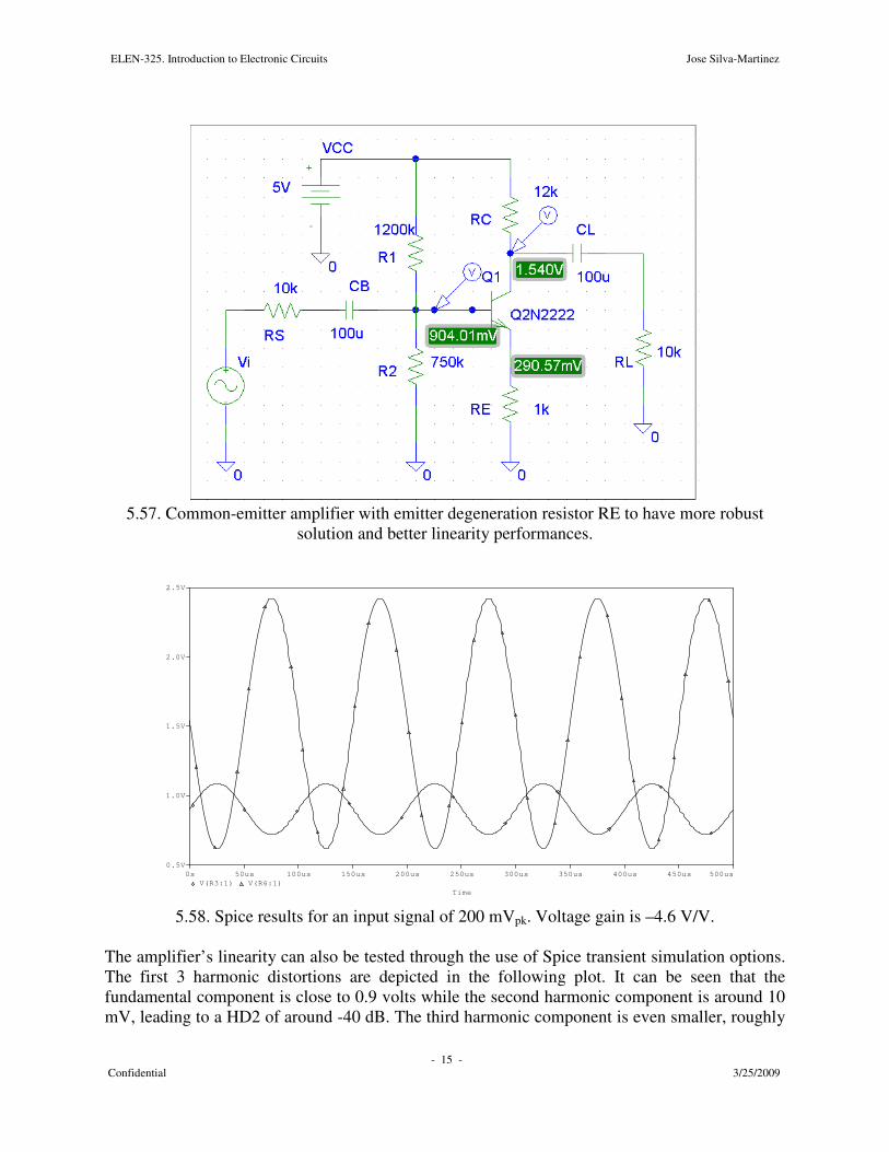
The main limitation of the circuit comes from the required input impedance (zi≈βRE). This constraint requires to increase the resistance attached to the emitter RE hence requiring even larger resistances at the collector terminal to afore the required voltage gain. This fact further limits the use of large collector current since large DC voltage drops across the emitter and collector resistances must be avoided, otherwise we do not have room for signal swing. The circuit has been simulated in SPICE; from fig. 5.56 the selected collector current is 300 µA, and the collector resistance is 10 kΩ. The schematic and component values are shown below. The resistors RB1 and RB2 were selected to be very large in order not to degrade the input impedance; RB=460 k is used. The final design is shown in figure below. The DC volategs are also shown to verify our assumptions. Since the β of the device is greater than the value used in the hand calculations, the collector current is roughly 290 µA. Before you run the simulations, please double check the DC operating point of the circuit; verify the VCE voltage and the collector current. The circuit was simulated in Pspice, and the transient response for a sinewave nput signal of 200 mVpk is shown in the followingn plot. The AC signal at the base terminal of the transistor has a DC component of 0.96 V, while the DC component of the output signal is around 1.5 V. The amplitude of the AC signal at the base is around 190 m Vpk, shown that the input impedance is close to 100 k, as expected. The output voltage is close 0.92 Vpk, leading to an overall voltage gain of -4.6. The small voltage gain is smaller than the expected -5 V due to the attenuation factor at the input stage of the amplifier, not taken into account in equation 5.55a. Since RS=10 k and the input impedance is around 100 k, there is an attenuation factor in that interface of 10k/(100k+10k)=0.909, leading to a theoretical voltage gain of -4.54, that fits very well with Spice results. The frequency response can also be obtained from Spice by using the AC-analysis option; although the magnitude and phase repsonses are not shown, we encourage the reader to obtain that plot; it will be found that the amplifier’s bandwidth (-3 dB frequency) is in the range of 100 MHz; for the design examples discussed in section 5.7, amplifier’s bandwidth is around 20-30 MHz. This is another property of the circuits, the bandwidth is smaller for high-gain amplifiiers.
AV=-10 =-7.5
Equation 5.61 (Vomax=1 Vpk)
Equation 5.59b (AV=-5)
Acceptable solution
ELEN-325. Introduction to Electronic Circuits Jose Silva-Martinez
- 15 - Confidential 3/25/2009
5.57. Common-emitter amplifier with emitter degeneration resistor RE to have more robust
solution and better linearity performances.
Time
0s 50us 100us 150us 200us 250us 300us 350us 400us 450us 500usV(R3:1) V(R6:1)
0.5V
1.0V
1.5V
2.0V
2.5V
5.58. Spice results for an input signal of 200 mVpk. Voltage gain is –4.6 V/V.
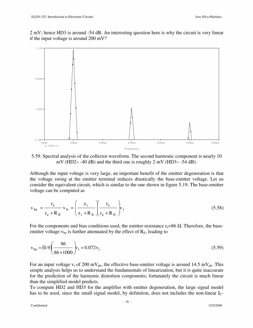
The amplifier’s linearity can also be tested through the use of Spice transient simulation options. The first 3 harmonic distortions are depicted in the following plot. It can be seen that the fundamental component is close to 0.9 volts while the second harmonic component is around 10 mV, leading to a HD2 of around -40 dB. The third harmonic component is even smaller, roughly
ELEN-325. Introduction to Electronic Circuits Jose Silva-Martinez
- 16 - Confidential 3/25/2009
2 mV; hence HD3 is around -54 dB. An interesting question here is why the circuit is very linear if the input voltage is around 200 mV?
Frequency
5KHz 10KHz 15KHz 20KHz 25KHz 30KHz 35KHzV(R6:1)
1.0mV
10mV
100mV
1.0V
5.59. Spectral analysis of the collector waveform. The second harmonic component is nearly 10
mV (HD2~ -40 dB) and the third one is roughly 2 mV (HD3~ -54 dB).
Although the input voltage is very large, an important benefit of the emitter degeneration is that the voltage swing at the emitter terminal reduces drastically the base-emitter voltage. Let us consider the equivalent circuit, which is similar to the one shown in figure 5.19. The base-emitter voltage can be computed as
iEe
e
Si
ib
Ee
ebe v
Rr
r
Rz
zv
Rr
rv
+
+=
+= (5.58)
For the components and bias conditions used, the emitter resistance re=86 . Therefore, the base-emitter voltage vbe is further attenuated by the effect of RE, leading to
( ) iibe v072.0v100086
869.0v =
+= (5.59)
For an input voltage vi of 200 mVpk, the effective base-emitter voltage is around 14.5 mVpk. This simple analysis helps us to understand the fundamentals of linearization, but it is quite inaccurate for the prediction of the harmonic distortion components; fortunately the circuit is much linear than the simplified model predicts. To compute HD2 and HD3 for the amplifier with emitter degeneration, the large signal model has to be used, since the small signal model, by definition, does not includes the non-linear IC-
ELEN-325. Introduction to Electronic Circuits Jose Silva-Martinez
- 17 - Confidential 3/25/2009
VBE characteristics of the transistor. In appendix 5A is shown that the second and third harmonic distortion components are given by the following expressions
+
== −
−CQ
pkc
th
CQEpkc
2
I
i
v
IR1
1
4
1i
2
kHD2 (5.60)
2
CQ
pkc2
th
CQE
th
CQE
2pkc
3
I
i
v
IR1
v
IR21
24
1i
4
kHD3
+
−
== −
− (5.61)
If the numerical values used in the previous example are used, then: ICQRE=290 mV, ICQRE/Vth=11.6 and HD2 and HD3 yields,
5.0I
iifdB40~
I
i021.0HD2
CQ
pkc
CQ
pkc =−
≅ −−
5.0I
iifdB56~
I
i0058.0HD3
CQ
pkc
2
CQ
pkc =−
≅ −−
Notice that these values fit very well with the results obtained from Spice. 5.11. Multi-satge amplifiers.
1st stagePoweramp
LOAD
Actuator2nd stage Nth stage
vi
RS
Sensor
Fig. 5.60 This section must include: Amplifier’s representation using input and output impedances, and transconductance or voltage gain

ELEN-325. Introduction to Electronic Circuits Jose Silva-Martinez
- 18 - Confidential 3/25/2009
VCC
RCvC
RB1
RB2
vBCB
RL
v0
CL
RS
vi
Amplifier
RE
RE
reie
αie RC
v0
RB
ixzi
vx
ibz0
i0
(a) (b)
ziv0
z0
RL
v0
RS
vi +-vb
+
-
+
-
Avvb
Amplifier
(c)
Fig. 5.61. Expressions for the input impedance, open-loop gain and output impedance will be given here. In the following analysis we assume that RB>>βRE>>rπ. The input impedance of this topology is given as:
( )( ) ( ) BEBEe
Rx
bi RRrR1Rr
i
vz
L
β+≅β++== π∞=
(5.62)
Form the small signal analysis of the circuit, the amplifier’s voltage gain is determined by the following expression
Eth
CQ
Cth
CQ
Em
Cm
Rb
0V
RV
I1
RV
I
Rg1
Rg
v
vA
L +−=
+−==
∞=
(5.63)
C
0v0
00 R
i
vz
b
===
(5.64)
ELEN-325. Introduction to Electronic Circuits Jose Silva-Martinez
- 19 - Confidential 3/25/2009
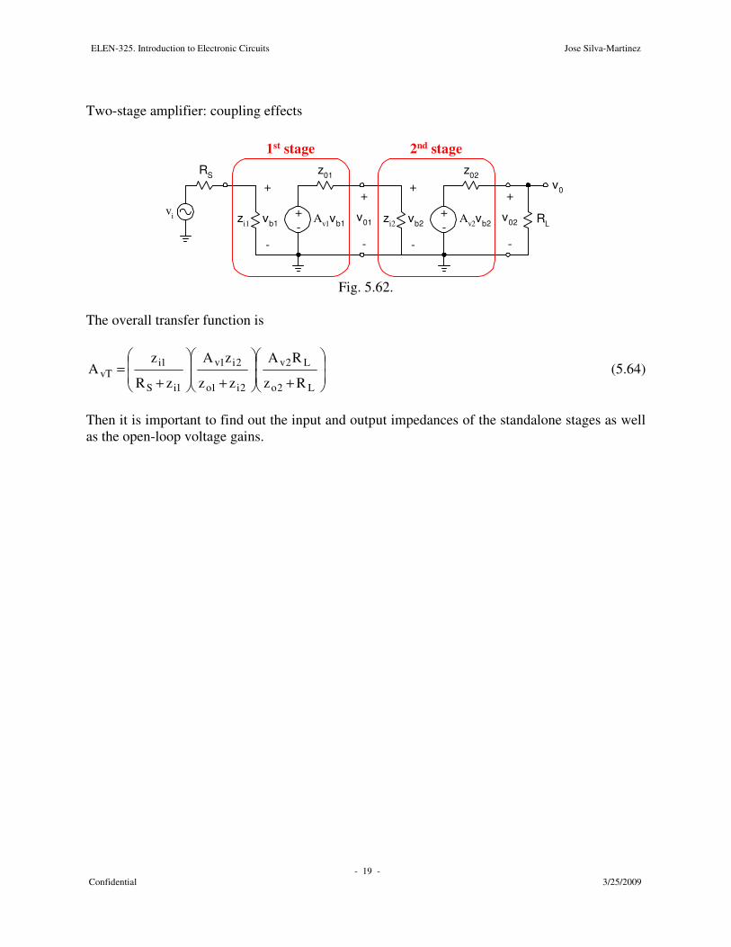
Two-stage amplifier: coupling effects
zi1v01
z01
RL
v0
RS
vi +-
vb1
+
-
+
-
Av1vb1
1st stage
zi2v02
z02
+-
vb2
+
-
+
-
Av2vb2
2nd stage
Fig. 5.62.
The overall transfer function is
+
+
+=
L2o
L2v
2i1o
2i1v
1iS
1ivT
Rz
RA
zz
zA
zR
zA (5.64)
Then it is important to find out the input and output impedances of the standalone stages as well as the open-loop voltage gains.
ELEN-325. Introduction to Electronic Circuits Jose Silva-Martinez
- 20 - Confidential 3/25/2009
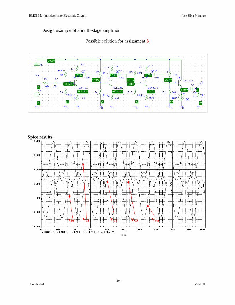
Design example of a multi-stage amplifier
Possible solution for assignment 6.
Spice results.
vB1 VC1 VC2 VC3 Vout
ELEN-325. Introduction to Electronic Circuits Jose Silva-Martinez
- 21 - Confidential 3/25/2009
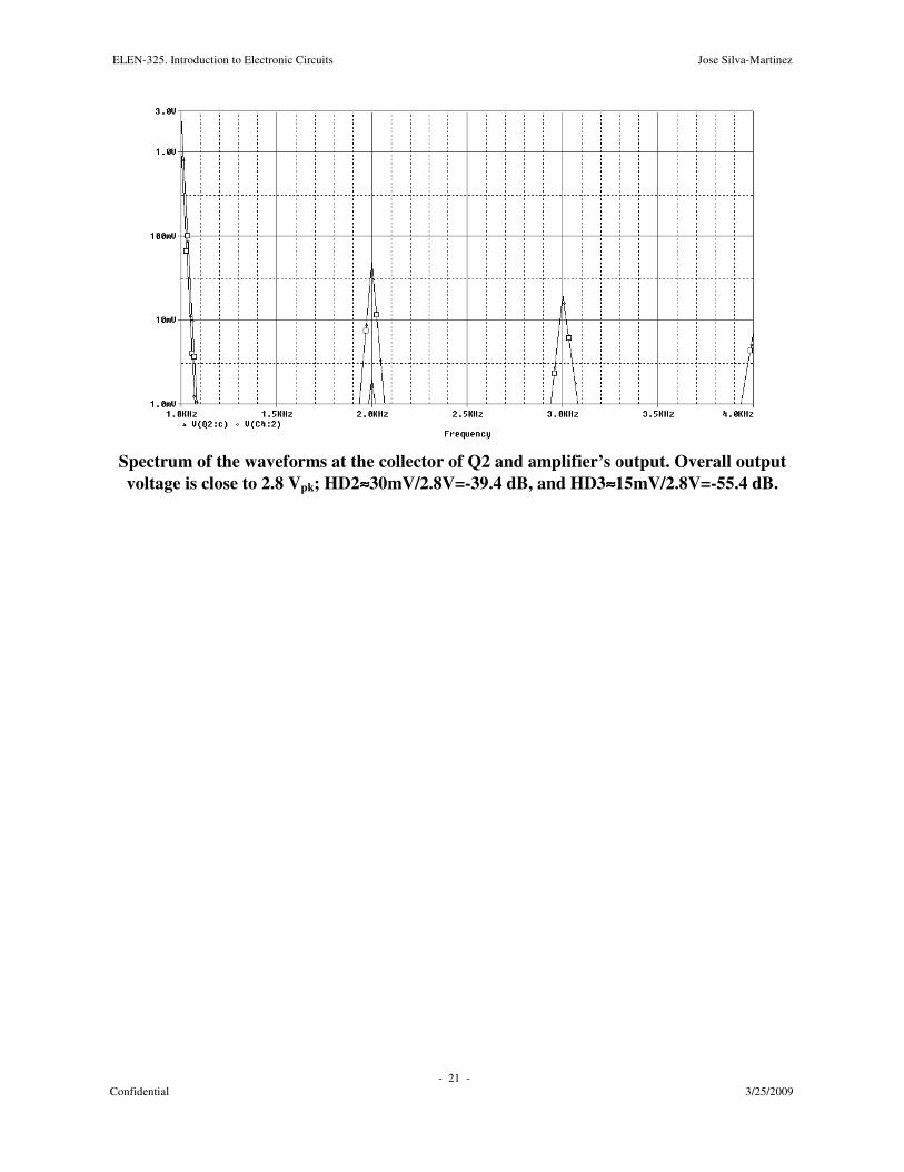
Spectrum of the waveforms at the collector of Q2 and amplifier’s output. Overall output voltage is close to 2.8 Vpk; HD2≈≈≈≈30mV/2.8V=-39.4 dB, and HD3≈≈≈≈15mV/2.8V=-55.4 dB.
ELEN-325. Introduction to Electronic Circuits Jose Silva-Martinez
- 22 - Confidential 3/25/2009
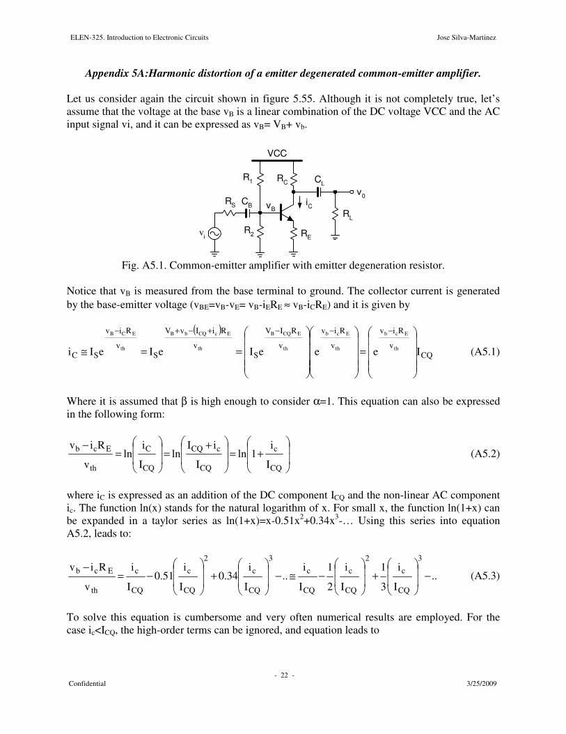
Appendix 5A:Harmonic distortion of a emitter degenerated common-emitter amplifier. Let us consider again the circuit shown in figure 5.55. Although it is not completely true, let’s assume that the voltage at the base vB is a linear combination of the DC voltage VCC and the AC input signal vi, and it can be expressed as vB= VB+ vb.
VCC
RC
iC
R1
R2
vB
RE
CBRSRL
v0
CL
vi
Fig. A5.1. Common-emitter amplifier with emitter degeneration resistor.
Notice that vB is measured from the base terminal to ground. The collector current is generated by the base-emitter voltage (vBE=vB-vE= vB-iERE ≈ vB-iCRE) and it is given by
( )
CQv
Riv
v
Riv
v
RIV
Sv
RiIvV
Sv
Riv
SC IeeeIeIeIi th
Ecb
th
Ecb
th
ECQB
th
EcCQbB
th
ECB
=
==≅
−−−+−+−
(A5.1)
Where it is assumed that β is high enough to consider α=1. This equation can also be expressed in the following form:
+=
+=
=
−
CQ
c
CQ
cCQ
CQ
C
th
Ecb
I
i1ln
I
iIln
I
iln
v
Riv (A5.2)
where iC is expressed as an addition of the DC component ICQ and the non-linear AC component ic. The function ln(x) stands for the natural logarithm of x. For small x, the function ln(1+x) can be expanded in a taylor series as ln(1+x)=x-0.51x2+0.34x3-… Using this series into equation A5.2, leads to:
..I
i
3
1
I
i
2
1
I
i..
I
i34.0
I
i51.0
I
i
v
Riv3
CQ
c
2
CQ
c
CQ
c
3
CQ
c
2
CQ
c
CQ
c
th
Ecb −
+
−≅−
+
−=
− (A5.3)
To solve this equation is cumbersome and very often numerical results are employed. For the case ic<ICQ, the high-order terms can be ignored, and equation leads to
ELEN-325. Introduction to Electronic Circuits Jose Silva-Martinez
- 23 - Confidential 3/25/2009
3
CQ
c
2
CQ
c
CQ
c
th
CQE
th
b
I
i
3
1
I
i
2
1
I
i
v
IR1
v
v
+
−
+≅ (A5.4)
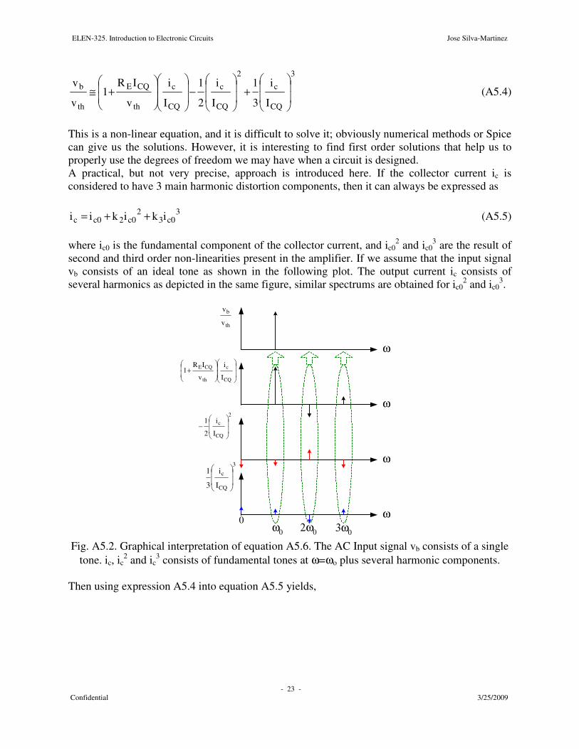
This is a non-linear equation, and it is difficult to solve it; obviously numerical methods or Spice can give us the solutions. However, it is interesting to find first order solutions that help us to properly use the degrees of freedom we may have when a circuit is designed. A practical, but not very precise, approach is introduced here. If the collector current ic is considered to have 3 main harmonic distortion components, then it can always be expressed as
3c03
2c02c0c ikikii ++= (A5.5)
where ic0 is the fundamental component of the collector current, and ic0
2 and ic03 are the result of
second and third order non-linearities present in the amplifier. If we assume that the input signal vb consists of an ideal tone as shown in the following plot. The output current ic consists of several harmonics as depicted in the same figure, similar spectrums are obtained for ic0
2 and ic03.
ω
ω
ω
ω0 2ω0 3ω0
ω0
th
b
v
v
+
CQ
c
th
CQE
I
i
v
IR1
2
CQ
c
I
i
2
1
−
3
CQ
c
I
i
3
1
Fig. A5.2. Graphical interpretation of equation A5.6. The AC Input signal vb consists of a single
tone. ic, ic2 and ic
3 consists of fundamental tones at ω=ωo plus several harmonic components. Then using expression A5.4 into equation A5.5 yields,

ELEN-325. Introduction to Electronic Circuits Jose Silva-Martinez
- 24 - Confidential 3/25/2009
−
+++
+
++−
++
+
=
..I
ikiki
3
1
I
ikiki
2
1
I
ikiki
v
IR1
v
v
3
CQ
3c03
2c02c0
2
CQ
3c03
2c02c0
CQ
3c03
2c02c0
th
CQE
th
b (A5.6a)
or
( )
( ) ( )
−+−
++
+
+−
++
−
+
=
3
CQ
c0CQ2
2CQ3
th
CQE
2
CQ
c0CQ2
th
CQE
CQ
c0
th
CQE
th
b
I
i..
3
1IkIk
v
IR1
I
i..
2
1Ik
v
IR1
I
i
v
IR1
v
v (A5.6b)
Although it is very difficult to find the exact solution for this equation, simple observations lead to very simple and relatively accurate results. First at all, the spectrum of the right hand side term is proportional to vb, and in a first approximation it consists of a single tone if an ideal sinusoidal is applied to the amplifier. Hence, the combination of all spectrums at the right-hand side of equation A5.6 must consists of a single tone as well, because the two spectrums have to be equal. According to equation A5.6, the right hand side coefficients of this expression must be zero with the exception of the first one, which defines the small signal transconductance of the amplifier. Therefore, it follows that
( )
( ) ( ) 03
1IkIk
v
IR1
02
1Ik
v
IR1
I
i
v
IR1
v
v
CQ22
CQ3th
CQE
CQ2th
CQE
CQ
c0
th
CQE
th
b
≅+−
+
≅−
+
+=
(A5.7)
Thus, the small signal transconductance becomes
ELEN-325. Introduction to Electronic Circuits Jose Silva-Martinez
- 25 - Confidential 3/25/2009
bEm
mb
th
CQE
th
CQ
c0 vRg1
gv
v
IR1
v
I
i
+=
+
= (A5.8)
Which fits with the small signal analysis done for this circuit in previous sections; overall voltage gain is obtained by taking into account the input voltage divider (zi/(zi+RS), the small signal transconductance gain given by A5.6, and the overall load resistance. The overall linearized voltage gain is then obtained as
iEm
LCm
Si
i0 v
Rg1
R||Rg
Rz
zv
+
+−= (A5.9)
This expression is similar to the one given in table 5.1. The coefficients k2 and k3 are computed as
( )
( ) ( )
+
−
=
+
+−=
+
=
2CQ
2
th
CQE
th
CQE
2CQ
th
CQE
CQ23
CQth
CQE2
Iv
IR1
v
IR21
6
1
Iv
IR1
1
3
Ik31k
Iv
IR1
1
2
1k
(A5.10)
Therefore, the second and third harmonic distortions can be approximated as follows
+
== −
−CQ
pkc
th
CQEpkc
2
I
i
v
IR1
1
4
1i
2
kHD2 (A5.11)
ELEN-325. Introduction to Electronic Circuits Jose Silva-Martinez
- 26 - Confidential 3/25/2009
2
CQ
pkc2
th
CQE
th
CQE
2pkc
3
I
i
v
IR1
v
IR21
24
1i
4
kHD3
+
−
== −
− (A5.12)
If the numerical values used in the previous example are used, then: ICQRE=290 mV, ICQRE/Vth=11.6 and HD2 and HD3 yields,
5.0I
iifdB40~
I
i021.0HD2
CQ
pkc
CQ
pkc =−
≅ −−
5.0I
iifdB56~
I
i0058.0HD3
CQ
pkc2
CQ
pkc =−
≅ −−
These values are in good agreement with the ones obtained from Spice.


![BJT or FET Transistor Configurations - MITweb.mit.edu/6.101/www/s2017/handouts/L05_4.pdf · ... Common Emitter Amplifier [b] Common Collector ... complicated circuit using basic properties](https://static.fdocuments.us/doc/165x107/5b1688a87f8b9a5e6d8c7917/bjt-or-fet-transistor-configurations-common-emitter-amplifier-b-common.jpg)