520 DEVELOPMENT OF ASTRONOMICAL OBSERV … · nasa-cr-152, 046 (nasa-cr-1 520 46) development of...
78
NASA-CR-152, 046 (NASA-CR-1 520 46) DEVELOPMENT OF N78 10983 DOPED-GERANIUM PHOTOCONDUCTORS FOR ASTRONOMICAL OBSERV-ATIONS AT WAVELENGTHS Pc40'57 Fi .40j FROM 30-TO 120 MICROMETERS Final-Technical uclas Report, 1 Oct.. 1976 (Santa Barbara Research G3/89 52034 FINAL TECHNICAL REPORT DEVELOPMENT OF DOPED-GERMANI'UM PHOTOCONDUCTORS FOR ASTRONOMICAL OBSERVATIONS AT WAVELENGTHS FROM 30 TO 120 MICROMETERS Contract No. NASZ-9385 For - National Aeronautics and Space Administration Ames Research Center Moffett Field, CA 94035 :t -. '4 ". ~ CENTER --------------- SANTA BARIBARA RESEARCH R---- A Subsidiary of Hughes Aircraft Company -S- ...... https://ntrs.nasa.gov/search.jsp?R=19780003040 2018-07-03T07:56:58+00:00Z
Transcript of 520 DEVELOPMENT OF ASTRONOMICAL OBSERV … · nasa-cr-152, 046 (nasa-cr-1 520 46) development of...

NASA-CR-152 046
(NASA-CR-1 520 46) DEVELOPMENT OF N78 10983 DOPED-GERANIUM PHOTOCONDUCTORS FOR ASTRONOMICAL OBSERV-ATIONS AT WAVELENGTHS Pc4057 Fi40j FROM 30-TO 120 MICROMETERS Final-Technical uclas Report 1 Oct 1976 (Santa Barbara Research G389 52034
FINAL TECHNICAL REPORT
DEVELOPMENT OF DOPED-GERMANIUM PHOTOCONDUCTORS FOR ASTRONOMICAL OBSERVATIONS AT WAVELENGTHS FROM 30 TO 120 MICROMETERS
Contract No NASZ-9385
For - National Aeronautics and Space Administration Ames Research Center Moffett Field CA 94035
t- 4 ~
CENTER ---------------SANTA BARIBARA RESEARCH R----A Subsidiary of Hughes Aircraft Company -S-
httpsntrsnasagovsearchjspR=19780003040 2018-07-03T075658+0000Z
NASA-CR-15Z 046
SANTA BARBARA RESEARCH CENTER A Subsidiary oj Hughes Aircraft Company
75 COROMAR DRIVE GOLETA CALIFORNIA
FINAL TECHNICAL REPORT
DEVELOPMENT OF DOPED-GERMANIUM
PHOTOCONDUCTORS FOR ASTRONOMICAL OBSERVATIONS
AT WAVELENGTHS FROM 30 TO 120 MICROMETERS
Contract No NASZ-9385
For
National Aeronautics and Space Administration Ames Research Center
Moffett Field CA 94035
31 October 1977
Prepared bamp(ampZAI
PR Bratt Senior Scientist
and 4 6 Approved by N N Lewis L E Long Project Engineer Project Manager
---- B R--------
PREFACE
This report describes the results of a technology development program
directed toward the optimization of the performance of beryllium-doped
germanium (Ge Be) and gallium-doped germanium (GeGa) infrared detectors
operating near 3 0 K at low backgrounds (108 photonsseccm 2 ) and low
frequencies ( 0 05 Hz) The work was performed at the Santa Barbara
Research Center over the period from 1 October 1976 to 31 March 1977
The Project Manager during the first half of the work was Peter R
Bratt During the second half Lawrence E Long undertook the manageshy
ment responsibility The Project Engineer was Nancy N Lewis The
Project Technical Monitor for NASAAmes was Craig McCreight A
number of other people at SBRC made significant contributions to this project
Roger A Cole and Eugene D Van Orsdell grew the GeGa and GeBe crystals
Kurt R Winrich David J Calhoun and James B Knutsen made the Hall
effect measurements and data analysis Beulah L Marolf fabricated
detectors and Courtney W Manker and Fred J Strobach assisted in the
design and assembly of the low-background test fixtures Richard L Nielsen
provided valuable assistance in trouble shooting test problems and evaluation
of test results We are also indebted to W J Moore of the U S Naval
Research Laboratories for helpful suggestions during the course of this work
SANTA BARBARA RESEARCH CENTER 11
--- RC
CONTENTS
Section Page
1 INTRODUCTION AND SUMMARY I-1
2 REVIEW OF PREVIOUS WORK 2-I
3 GeGa CRYSTAL GROWTH AND EVALUATION 3-1
Crystal Growth 3-1
Doping Concentration 3-1
Hall Mobility 3-5
Resistance Versus Temperature 3-6
4 GeBe CRYSTAL GROWTH AND EVALUATION 4-1
4-1
4-4
4-9
4-9
4-12
GeBe Crystal Growth
GeBe Crystal Evaluation
Hall Mobility
Resistance Versus Temperature
Impact Ionization Breakdown
5 DETECTOR FABRICATION AND TEST
Detector Fabrication 5-1
5-1
Low Background Test Dewars 5-1
Test Procedure 5-7
Results - GeGa Detectors 5-8
Results - GeBe Detectors 5-19
6 CONCLUSIONS AND RECOMMENDATIONS FOR FUTURE WORK 6-1
GeGa Detectors 6-1
GeBe Detectors 6-Z
Recommendations for Future Work 6-2
SANTA BARBARA RESEARCH CENTER iii
SBRC
CONTENTS (Cont)
Appendix Page
A IRRADIANCE CALCULATIONS A-1
GeGa Test Dewar A-1
GeBe Test Dewar A-5
B DETECTOR RESISTANCE MEASUREMENTS THROUGH MOSFET B-1
SANTA BARBARA RESEARCH CENTER iv
ILLUSTRATIONS
Figure Page
3-1 GeGa Single Crystal Ingot No 4 3-Z
3-2 Doping Profile for GeGa Ingot No 4 Produced by a Zone Leveling Technique 3-Z
3-3 Hall Coefficient Versus Reciprocal Temperature for Sample No GeGa 4-la 3-4
3-4 Hall Coefficient Versus Reciprocal Temperature for Sample No GeGa 4-3a 3-4
3-5 Hall Mobility Versus Temperature for Three Samples from Crystal GeGa 4 3-7
3-6 Circuit Used for Resistance Versus Temperature
Measurements on Detector Samples 3-7
3-7 Resistance Versus Reciprocal Temperature for Two GeGa Detector Samples from Crystal 4 (QB 0) 3-8
4-i Doping Profiles for Two GeBe Ingots 4-5
4-2 Hall Coefficient Versus Reciprocal Temperature for Sample No GeBe 9-z 4-7
4-3 Hall Coefficient Versus Reciprocal Temperature for Sample No GeBe 9-3 4-7
4-4 Hall Coefficient Versus Reciprocal Temperature for Sample No GeBe 10-3 4-8
4-5 Hall Mobility Versus Temperature for Four GeBe Samples 4-10
4-6 Resistance Versus Reciprocal Temperature for Four Uncompensated GeBe Detector Samples (QB - 0) 4-Il
4-7 Conductance Versus Electric Field Strength for GeBe Detector Samples at 4 Z0 K (QB 0) 4-13
4-8 Conductance Versus Electric Field Strength for GeBe Detector Samples at 3 45 0 K (QB 0) 4-13
5-1 Detector - Cryogenic Preamplifier Assembly 5-2
5-Z Sketch of Copper Heat Sink for Mounting Detector-Preamplifier Assemblies to the Low-Background Test Dewar 5-2
SANTA BARBARA RESEARCH CENTER v
ILLUSTRATIONS (Cont)
Figure Page
5-3 Low-Temperature Low-Background Dewar Setup for Testing of GeGa Detectors at 100 prm 5-4
5-4 Low-Temperature Low-Background Dewar Setup for Testing GeBe Detectors 5-4
5-5 Diagram of Circuit Used for GeGa and GeBe Detector Tests 5-8
5-6 Resistance Versus Temperature for GeGa Detectors 5-10
5-7 Signal Noise NEP and DC Resistance Versus Bias Voltage for GeGa Detector No 4-lbl-1 at Two Temperatures (10 Hz Data) 5-10
5-8 Signal and Noise Versus Frequency for GeGa Detectors at3 0K 55-1Z
5-9 Signal and Noise Versus Frequency for GeGa Detectors at Z 00 K 5-13
5-10 NEP Versus Frequency for GeGa Detectors at 3 00 K 5-17
5-11 NEP Versus Frequency for GeGa Detectors at Z 00 K 5-l7
5-1Z NEP Versus Temperature for GeGa Detectors at a Frequency of 10 Hz 5-18
5-13 NEP Versus Frequency for GeGa Detector 4-5b-i at 3 00K for Four Different Background Flux Levels 5-18
5-14 Signal Noise NEP and DC Resistance Versus Detector Voltage for GeBe 10-3a-3 at Two Temperatures ZK and 30 K 5-Z0
5-15 Resistance Versus Detector Temperature of GeBe Detectors 5-Z0
5-16 Signal and Noise Versus Frequency for GeBe Detectors at 3 0 K 5-ZZ
5-17 Signal and Noise Versus Frequency for GeBe Detectors at 2 0 K 5-Z3
5-18 NEP Versus Frequency for GeBe Detectors at 3 00 K 5-Z5
5-19 NEP Versus Frequency for GeBe Detectors at Z 00 K 5-Z5
5-Z0 NEP Versus Detector Temperature for GeBe Detectors 5-Z6
SANTA BARBARA RESEARCH CENTER vi
SBRC
ILLUSTRATIONS (Cont)
Figure Page
A-I Relative Spectral Response of GeGa Detector with Long Wavelength Pass Filter A-Z
A-Z Relative Spectral Response of GeBe Detector with Band-Pass Filter A-6
B-I Circuit Diagram for Low- Background Detector Testing B-i
SANTA BARBARA RESEARCH CENTER vii
TABLES
Table Page
3-1 Summary of Doping Parameters Crystal No 4
for GeGa 3-5
4-1 Impurity Concentrations in Three Germanium Samples
(in parts per million atomic ppma) 4-3
4-Z Doping Parameters Obtained from Theoretical
Four-Level Model to GeBe Hall Samples Fit of
4-8
5-1 List of Parameters Calculations
Used in Blackbody Irradiance 7
5-Z Parameters Used in Calculation of Short-Circuit
Current Responsivity for GeGa Detectors 5-15
5-3 Parameters Used in Calculation of Short-Circuit
Current Responsivity for GeBe Detectors 5-Z4
A-I Listing by Spectral Interval of Blackbody Signal Radiant
Emittance and Background Photon Flux Values Used for
GeGa Detector Testing A-3
A-Z Listing by Spectral Interval of Blackbody Signal Radiant
Emittance and Background Photon Flux Values Used for
GeBe Detector Testing A-7
B-1 Resistance Versus Temperature of Typical Load Resistor Used in IRAS Device Assemblies B-Z
viiiSANTA BARBARA RESEARCH CENTER
Section 1
INTRODUCTION AND SUMMARY
The work described in this report was a continuation of a previous
technology development program on GeBe and GeGa detectors which was
funded by NASAGoddard and administered by iitt Peak National Observatory
During the previous phase of this work emphasis was on GeGa detector
development During this new phase more emphasis was placed on GeBe
detector development
The ultimate goal of this work was to develop the technology for producshy
tion of doped-germanium detectors which have optimized performance in the
30- to 120- an wavelength range and are capable of achieving the objectives
of the Infrared Astronomy Satellite (IRAS) space mission
Because of the short period of performance for the work performed
on this phase it was not expected that the technology for producing fully
optimized detectors would be totally developed However significant advanceshy
ment was anticipated A future development phase is considered to be
necessary to continue the development work
The work of this phase was divided into the following major tasks
1 Growth of GeGa crystals from high-purity starting material with Ga concentrations different from that previously produced and development of a zone leveling method to produce a uniform Ga doping concentration
2 Growth of uncompensated GeBe crystals from high-purity starting material with a range of Be concentrations between 1X 10¹⁴ and 1x 10¹⁶ atomscm 3
3 Evaluation of crystals by means of Hall effect and resistance measurements as a function of temperature
4 Fabrication and test of detectors made from both GeBe and GeGa crystals to determine the relative performance between different crystals Correlation of detector test data with material evaluation data and analysis of how to further optimize detector performance
SANTA BARBARA RESEARCH CENTER 1-1
-SBRC
All these tasks were successfully completed during the course of the
program The results of this phase may be summarized as follows
The zone leveling technique for growing GeGa crystals was impleshy
mented and shown to produce a uniform Ga doping concentration over more than 5 inches of ingot length This established a reliable
material production method which yields a quantity of detector material more than adequate for the IRAS focal plane array (FPA) fabrication
GeGa detectors made from the zone leveled material showed someshy
what lower NEP values than any made previously at SBRC The best
measured NEP was 4 X 10 - 1 7 wattsHzi at a wavelength of 100 jim a frequency of 1 Hz an operating temperature of 3 0degK and a
background flux of 4 X 10⁸ photonsseccm Z
Tests on a number of GeGa detectors showed a high yield of good
elements and excellent uniformity between different elements The
detector fabrication technology appears to be adequate for fabrication of a large focal plane array such as that required for the IRAS mission
Growth of GeBe crystals proved to be difficult because of small
amounts of oxygen in the zone melting furnace which either formed a Be-O compound on the surface of the ingot or a Be-O complex inside
the ingot In either case Be is effectively removed to an inactive site
and cannot produce impurity photoconductivity The problem was solved by growing GeBe crystals under vacuum This yielded a
small amount of material for detector test and evaluation however uniformly doped GeBe ingots were not obtained and the control of
Be doping concentration was not as good as for Ga doping Further
work on the GeBe crystal growth technology is warranted
The maximum limit on Be doping concentration established by impurity hopping conductivity was determined to be Z-3 X 10¹⁵
atomscm 3
GeBe detectors made on this program achieved NEP values of 3 X 10-16 wattsHz at a wavelength of 40 jim a frequency of I Hz an operating temperature of 3 0 0 K and a background flux of 7 X 10⁸ photonsseccm z
The yield of GeBe detectors was acceptable However these detectors do not seem to be operating as close to the theoretical
background limited performance (BLIP) standard as do the GeGa detectors
SANTA BARBARA RESEARCH CENTER 1-2
rSBRCy
In general it may be concluded from this work that GeGa developshy
ment is essentially complete and this material should adequately serve for
the long-wavelength detector array in the IRAS FPA Minor technology
improvements such as a slightly higher Ga doping concentration and the
use of integrating cavities should further improve detector performance
Work on GeBe is not complete Further development of the crystal
growth technology is necessary to have a reliable doping method It is also
of interest to grow compensated GeBe crystals and compare detector pershy
formance to the uncompensated material that has been used up to this point
in time
SANTA BARBARA RESEARCH CENTER 1-3
Section Z
REVIEW OF PREVIOUS WORK
Previous work involved exploratory developmentin GeGa crystal
growth as well as detector fabrication technology using both GeGa and GeBe
material GeGa detectors were made from material furnished by the Naval
Research Laboratories (W J Moore) and from material produced at SBRC
GeBe detectors were made only from material furnished by NRL The
results of the GeGa work were very encouraging in that the crystal growth
method used was shown to be capable of producing a specified Ga doping
concentration with very low concentrations of residual donor impurities - 1 6= 4 X10Detector performance was found to be reasonably good with NEP
1
wattHz2 at 100 Inn for a background flux of 18 X 1010 photonsseccm Z
and 13 X 10-16 wattHz2 for a background flux of 1 2 X 10⁹ photonsseccm z - 15
The GeBe1 detectors made from NRL material achieved an NEP of I X10
wattsHz 2 at 40 pim with a background flux of 19 X 109 photonsseccm z
This work clearly demonstrated the feasibility of these detector materials
as very sensitive detectors of long-wavelength radiation under low-temperature
and low-background conditions of operation It established a starting point
from which further technology development efforts could proceed and
fostered a confidence that the ultimate performance goals could be realzqj
within reasonable time and cost constraints
The zone melting method for growth of GeGa crystals was implemented
and found to work well After growth of a few crystals it was realized that
a more uniform Ga doping concentration should be attainable by going to a
zone leveling modification using the same furnace This became one of the
primary tasks for the follow-on program No previous experience with the
growth of GeBe crystals existed at SBRC so this also became a major new
task
Z-1SANTA BARBARA RESEARCH CENTER
Detector fabrication technology which had been previously developed
at SBRC for doped Ge detectors was found to work well on these longer waveshy
length materials In particular the use of ion implantation in the formation
df electrical contacts to the crystals was shown to give an ohmic contact with
little or no excess noise for frequencies down to 1 Hz
The fundamental principles of operation of a doped-germanium far
infrared detector were described in the Final Technical Report for the
previous phase of this program I The detector operates as an extrinsic
photoconductor Photoionization of the doping impurity atoms (Ga or Be)
by infrared radiation produces extra free holes in the crystal which increase
its conductivity This conductivity increase can be easily measured using a
suitable electrical circuit
The energy required for ionization of the Ga atoms in Ge is 0 011 eV
Thus incoming photons with an energy greater than this value can cause
photoionization those with a lesser energy cannot This requirement can be
expressed in terms of the infrared photons wavelength as follows
hc Ei (1)
where h is Plancks constant c the speed of light Xis the wavelength and
Ei is the ionization energy For energies expressed in eV and wavelength
in [Lm Equation (1) can be rewritten as
X lt 1 4 ()
Thus photons of wavelength less than 100 jim can produce photoconductivity
in GeGa crystals The Be atom in Ge has an ionization energy of 0 024 eV
Therefore photons of wavelength less than 5Z 4zm can produce photoconductivity
in GeBe crystals
1 P R Bratt Improved GeGa and GeBe Far Infrared Detector Development Final Technical Report Contract No 86310 (AURA) Santa Barbara Research Center Oct 1977
SANTA BARBARA RESEARCH CENTER Z-Z
R
The optimization of a detectors sensitivity involves an attempt to
maximize the photoconductive response and minimize the various noise
sources present either in the detector itself or in the associated- electrical
components
A theoretical analysis of detector operation under low background
conditions has pointed out the directions in which to proceed toward optimizashy
tion of detector performance These may be summarized as follows
1 Grow GeGa and GeBe crystals with doping concentrations as large as possible so as to maximize the responsive quAntum efficiency but keep the doping concentration below the point where impurity hopping conductivity begins to significantly lower detector resistance This implies that there is some optimum doping concentration which will be different for each type of impurity atom This concentration must be determined experimentally for the particular temperatures of operation and background photon flux levels expected in the IRAS mission
g Maximize the photoconductive gain of the detector by using material with long free-hole lifetime This mandates the use of high-purity Ge starting material with a very low concentrashytion of residual donor impurities Fabricate detector crystals with a minimum interelectrode spacing and operate with applied electric field strength as large as possible
3 Provide electrical contacts to the doped Ge crystal which do not produce excess noise and are ohmic for transport of charge carriers (free holes) into and out of the crystal
These guidelines formed the basis for the development efforts to be
carried out in the follow-on program described in this report
SANTA BARBARA RESEARCH CENTER 2-3
=SBRC
Section 3
GeGa CRYSTAL GROWTH AND EVALUATION
CRYSTAL GROWTH
One GeGa crystal was grown during this phase of the program A
zone leveling technique was used in an attempt to provide a more uniform
distribution of Ga in the crystal than was achieved in previous runs at SBRC
Also a higher doping concentration was used to see if material with a higher
quantum efficiency could be obtained
The method of Ge purification by multipass zone refining described in
the previous report was used Ga doping by means of the pellet dropping
spobn was also used However in this run the doping pellet was dropped
near the tail end of the ingot The molten zone was formed there moved
to the seed end then back to the tail end again completing the run Figure
3-1 shows a photograph of the finished GeGa ingot The seed end of the
crystal (with seed still attached) is to the left in this picture and the tail
end is to the right This crystal contains over 5 inches of uniformly doped
material in the central region of the ingot The seed end was subsequently
cut off for reuse and the tail end was cut off and discarded as scrap
DOPING CONCENTRATION
Samples were cut from the doped region at 1-inch intervals for evaluashy
tion by Hall effect measurements The Ga doping concentration was found
to be quite uniform over the whole 5-inch length which was evaluated The
results are shown in Figure 3-Z The average doping concentration was
a 5 x 10¹⁴ Ga atomscm 3 This provided high quality detector material with
a doping concentration Z 5 times greater than that used in our previous work
2 Op cit
SANTA BARBARA RESEARCH CENTER 3-1
1SBRC-1
yr
Figure 3-1 GeGa Single Crystal Ingot No 4
Note The seed end is to the left and the tail end to the right Over 13 cm of uniformly doped material is contained in the central region of this ingot
GeGa INGOT PROFILE
1 I I II III IS SEED _11 IIIII 1 INCH
la lb 2a 3a 3b 4a 5a 5b 6a SLICE NO 40
-o 3
C-) 2
O 1 opoO QUAL
0 I I I I
0 1 2 3 4 5 6 LENGTH ALONG INGOT (INCHES)
Figure 3-Z Doping Profile for GeGa Ingot No 4 Produced by a Zone Leveling Technique
SANTA BARBARA RESEARCH CENTER 3-2
11SBRC1
Evaluation of selected samples by means of Hall effect measurements
versus temperature was also done Comparison of experimental data points
with theoretically generated curves provides a determination of the residual
donor atom concentration in the crystal Details of the method of analysis
were given in the previous report Z Figures 3-3and 3-4 show experimentally
measured Hall coefficient data versus temperature and the theoretical fit
which was obtained for two of the three samples which were evaluated The
third sample GeGa No 4-5a was almost identical in behavior to No 4-3a
and is therefore not shown The last four low temperature experiemntal
data points in Figure 3-3 are in error due to limitations in the Hall effect
equipment and should be disregarded The rise in the high-temperature
data points above the theoretical line is due to the influence of a small populashy
tion of high-mobility holes in the light mass valence band which cause the
measured Hall coefficient to rise in this temperature range 3 This could be
eliminated by the use of higher magnetic field strengths in the Hall effect
measurement but our equipment was limited to a field strength of 5 000
gauss The effect does not interfere with the low-temperature data and
thus does not compromise the theoretical curve fitting procedure
Donor atom concentrations deduced from the comparison between
theoretical and experimental data are listed in Table 3-1 for all three
samples It is to be noted that the residual donor atom concentration in
3this crystal is in the 10 1 0 cm range whereas previous GeGa material had
3concentrations in the 10 1 1 cm range or higher The free-hole lifetime in
this material should therefore be higher than in any of the previously
grown crystals
The values of ionization energy are found to be somewhat higher than
the literature value of 0 0108 eV This result was also noted for our previdus
Ga-doped crystal GeGa 3 The reason for this is not presently known
Z Ibid
3 R K Willardson T C Harman and A C Beer Phys Rev 96
151Z (1954)
SANTA BARBARA RESEARCH CENTER 3-3
lOll
109
10
004 O6 04 010 02 014 016 00M 021) lIT IKl
0 u1
Figure 3-3 Hall Coefficient Versus Reciprocal Temperature
for Sample No GeGa 4-la
Note Open circles are experimental data points the solid line
is theoretical data calculated using the parameters given
in Table 3-1
loll
lo0
9 10
S10
a
106
a O 004 01 00 010 012 O14 006 al 020 IT [-]I
Figure 3-4 Hall Coefficient Versus Reciprocal Temperature for Sample No GeGa 4-3a
Note Open circles are experimental data points the solid line is theoretical data calculated using the parameters given
in Table 3- 1
SANTA BARBARA RESEAPCH CENTER JRIGINAL PAGE IS VF POOR QUALITY
3-4
BRCI
Table 3-1 Summary of Doping Parameters for GeGa Crystal No 4
Sample NA - ND NA ND Ei No (cmshy3 ) (cm - 3 ) (cm - 3 ) (eV)
X 10114 X 10 10
GeGa 4-la Z7 2 7 14 00114
-4-Za 26 - shy
4-3a Z5 Z5 95 00112
--4-4a Z3
4-5a 25 Z5 8 0 00113
--4-6a Z8
HALL MOBILITY
The Hall mobility is plotted versus temperature in Figure 3-5 for
all three of the samples cut from crystal GeGa 4 It is seen that they all
have essentially the same mobility values at all temperatures There is
some scatter in the data at temperatures below 7 0 K particularly for sample
4-la which is thought to be due to experimental error The data points for
the other two samples continue rising down to the lowest temperature of
5 50 K
No attempt was made to do a detailed analysis of the mobility data
Qualitatively it appears that the hole mobility in these samples is primarily
limited by lattice scattering because this is the only scattering mechanism
which permits the mobility to continue to rise as temperature is lowered
Ionized impurity scattering produces a mobility which decreases as
temperature is lowered and neutral impurity scattering causes the mobility
to be nearly independent of temperature At a low enough temperature
neutral inpurity scattering would be expected to become predominant and
limit further mobility increases JRIGINAL PAGE IS
OF POOR QUALITY
3-5SANTA BARBARA RESEARCH CENTER
SBRc-I
An estimate of the neutral impurity limited mobility may be calculated
from the formula of Sclar 4
1 17 X 10z (mImo) K T 30 2 (mfm ( K NN [ (mmo)2 K Ta
where m is the hole effective mass m o is the mass of an electron K is
the dielectric constant of Ge NN is the concentration of neutral scattering
centers and T is the absolute temperature
Using
mm = 0 Z8o
K = 16
NN = 2 5 X i0 14 cm3
we obtain values for IN in the vicinity of 8 X 10⁵ cmZvolt sec These are
plotted on Figure 3-5 for the temperature range between Z and 10 0K It
would not be unreasonable to assume that the measured data are approaching
this limit However further measurements in the Z to 60 K range would be
required to establish this for certain
RESISTANCE VERSUS TEMPERATURE
Because of equipment limitations the variable temperature Hall effect
measurements on GeGa samples could not be extended below 50 K This is
not due to a temperature limitation but because the sample impedance
becomes so high that the constant current supply on the Hall apparatus no
longer functions properly To obtain data attemperatures less than 50 K
a GeGa detector element was obtained and its resistance measured versus
temperature over the range from 100 to 3degK The main objective of this
measurement was to determine if impurity hopping conductivity was present
Figure 3-6 shows the circuit diagram used for the measurement Data were
taken with a constant voltage of 0 0Z volt applied across the sample producing
4 N Sclar Phys Rev 104 1559 (1956)
SANTA BARBARA RESEARCH CENTER 3-6
SSR
NEUTRALIMPURITYSCATTERINGLIMIT
0 G Ga4-1a
amp Gamp-Ga 4-3a
S t Ge-Ga4-5a
w
104
l I II L WLLL LLL 24plusmnI 1003110
TEMPERATURE(K(
Figure 3-5 Hall Mobility Versus Temperature for Three Samples from Crystal GeGa 4
SHIELDING
3K
1KW
KIEIIampEY6IB I j(LS VM ORIGINAL PAGE IS (CURREM) OQSI I K OF POOR QUAjITYI
SAMPLEIN VARIABLE
TEMPERATUREDEWAR
LW Figure 3-6 Circuit Used for Resistance Versus Temperature
Measurements on Detector Samples
SANTA BARBARA RESEARCH CENTER 3-7
---SBRC---------shy
an electric field strength of 0 4 voltcm A carbon resistor thermometer
mounted close to the detector sample was used for temperature measurement
Background radiation was excluded from the samples during the measurements
Figure 3-7 shows the results on two samples from crystal GeGa 4
These samples were taken from the same slice as were the detector samples
In fact they were surplus detector samples and were therefore fabricated
in the same manner as detector samples One sample shows a strict exposhy
nential dependence for resistance versus IT up to 1012 ohms The other
sample shows a slight variation from an exponential dependence in the
vicinity of 1011 ohms which may be due to some experimental error since
to obtain the highest resistance readings currents in the 10-14 ampere
range had to be measured It is concluded from these data that impurity
hopping conductivity is not a significant problem in these GeGa samples
with a Ga doping concentration of Z 5 X 10¹⁴ atomscm 3
l0
ORIGINAL PAGE IS
TOF POOR QUAL
Figure 3-7 Resistance Versus Reciprocal Temperature for Two GeGa Detector Samples from Crystal 4 (QB 0)
SANTA BARBARA RESEARCH CENTER 3-8
SBRC
Also to be noted in Figure 3-7 is the difference in resistance between
these two samples In the temperature range between 3 5 and 5K this
difference amounts to a factor between 5 and 6 Since both detector samples
were cut to the same dimensions and the hole mobility is the same in each
this implies a difference in the free-hole concentration of a factor between
5 and 6 In the temperature range of interest the free-hole concentration
is given by
ND iZrmkT exp (-EikT) (4)
where NA is the acceptor (Ga) concentration ND is the residual donor conshy
centration k is Boltzmanns constant h is Plancks constant Ei is the Ga
ionization energy and 6 is the ground state degeneracy of the Ga atom
Differences in free-hole concentration will be controlled by the acceptor
and donor doping concentration factor (NA - ND)ND From Table 3-1 using
values for NA and ND from slices 4-la and 4-5a (which were cut adjacent to
samples 4-lb and 4-5b) we calculate from this equation that the free-hole
concentration should differ by a factor of 6 Z and the sample with the lowest
ND value (4-lbl-2) will have the highest free-hole concentration and thereshy
fore the lowest resistance This is in good agreement with the measured
resistance data of Figure 3-7 These resistance data are -therefore confirmshy
ing evidence for the lower residual donor impurity concentration in the seed
end of GeGa crystal No 4
The ionization energies calculated from the slope of these resistance
versus lIT curves are in good agreement with the values obtained from Hall
coefficient data
SANTA BARBARA RESEARCH CENTER 3-9
-SBRC
Section 4
GeBe CRYSTAL GROWTH AND EVALUATION
GeBe CRYSTAL GROWTH
The initial GeBe crystals produced on this program were grown in
the same zone melting furnace used for GeGa crystal growth This furnace
was equipped with two doping spoons so that the doping alloy can be added to
the melt without opening the furnace to laboratory air Crystals were grown
in an atmosphere of hydrogen gas purified by passage through a hot palladium
membrane A GeBe doping alloy of approximately 0 01 atom percent was
prepared by meltfng together the appropriate amounts of high purity Ge and
Be in a quartz tube under hydrogen gas
In the first crystal growth run an amount of doping alloy was used
sufficient to produce about i015 Be atomscm 3 in the grown crystal The
calculation was based on a value for the distribution coefficient of Be in Ge
of 0 07 as reported by Shenker et al 5 It turned out that no Be was detected
by Hall effect measurements on the grown crystal Four more doping runs
were made with ever increasing additions of the Be doping alloy with essentially
the same result - no electrically active Be in the grown crystal Finally on
the sixth and seventh attempts using an exceptionally large amount of doping
alloy we were able to observe Be in the 1016 atomscm 3 range However
the concentration decreased rapidly in the direction along the crystal away
from where the doping pellets were placed and after about I inch no more
Be was detected
From these results it was concluded that Be must be going into the
crystal but most of it was being made electrically inactive by combining
with something probably oxygen The observation of an abnormal surface
5 H Shenker E M Swiggard and W J Moore Trans Metallurgical Soc
of AIME Z39 347 (1967)
SANTA BARBARA RESEARCH CENTER 4-1
--SBR
film on the top of the GeBe ingots was taken as possible evidence of BeO
which floats to the surface of the melt In addition Be atoms could be
complexed with oxygen in the bulk of the crystal This has been shown to
occur with boron-doped germanium 6
A check for Be and 0 in the bulk of the crystal was made using the mass
spectrographic analysis method Three samples were evaluated one from
crystal GeBe 5 and two from crystal GeBe 6 Crystal GeBe 5 showed no
electrically active Be in a Hall effect measurement Crystal GeBe 6 showed
electrically active Be in one sample (S-i) but essentially no Be in the other
The results of the mass spectrographic analyses are shown in Table 4-i
Because of interference from the 7 ZGe+ 8 line the detection of Be is someshy
what hampered However there is clear evidence of Be in sample GeBe
6-S-I The Hall effect measurement on this sample indicated 1 X10 1 6 atoms
cm 3 of electrically active Be which corresponds to 0 ZZ ppma The mass
spectrographic analysis indicates 65 ppma about 300 times the electrically
active amount There is also clear evidence of an ample supply of oxygen in
the crystal to complex with the Be Crystal GeBe 5 showed more than twice
the oxygen content of GeBe 6 Also of interest are the large concentrations
of the shallow acceptor atoms B and Al These concentrations are much
greater than would normally be detected in a Hall effect measurement and
indicate that oxygen complexing is also taking place with these atoms
From past work 7 8 it is known that oxygen is normally present in Ge
to a level of about 50 ppma although it has been noted 8 that the results will
vary depending on the method of crystal growth The mass spectrographic
analyses on our crystals showed much higher oxygen levels than normal
6 WD Edwards J Appl Phys 39 1784 (1968)
7 C D Thurmond W G Guldner and A L Beach J Electrochem Soc 103 603 (1956)
8 H A Papazian and S P Wolsky J AppI Phys Z7 1561 (1956)
SANTA BARBARA RESEARCH CENTER 4-Z
-SBRCI Table 4-i Impurity Concentrations in Three Germanium Samples
(in parts per million atomic ppma)
Detection GeBe 5 GeBe 6 GeBe 6Limit S-1 S-i S-2
Li 0 1 36 35 07 B 0 2 ND ND Z5 5 Be 10 0 20 0 65 0 10 0 O 03 1372 0 456 0 5650 Na 0 1 4Z 0 77 0 30 0 Mg 3 0 3 0 ND ND Al 0 7 35 0 91 5 23 0 Si 07 07 07 07 K 03 03 43 Z1 Ca 05 2Z 64 93 Cu 1 0 1 0 ND ND Ga 0 1 49 54 38 Ag 10 Z Z ND ND
Note Tantallum and gold are not reported since tantalum slits and gold foil are used Gallium is residual in the mass spectrometer Ge lines interfere with nitrogen and chlorine determination Other elements not detected have a detection limit of 5 ppma
Based on 1 X 10- 8 coulomb exposure
7 zGe + 8 interferes with Be determination The figures listed above are estimates based on the theoretical abundance ratio of Ge7Z to Ge74 isotopes (Measurements performed by Technology of Materials Santa Barbara California)
Because of the extensive zone refining done on the Ge before doping one
would have expected a lower oxygen content than normal From this result
a leak was suspected in the hydrogen purification system Indeed a leak
was found
Subsequent crystals were grown under vacuum with the objective
being to reduce the oxygen content in the melt by an out-gassing process
Three more crystals were grown during the remainder of this program
Crystal GeBe 8 was doped to Z X 1017 Be atomcm 3 using a single doping
SANTA BARBARA RESEARCH CENTER ORIGINALPAGEIS 4-3 OF POOR QUALITY
pellet addition at the seed end of the ingot Crystal GeBe 9 was incrementally
doped with Be to five different levels ranging from about 1 X 10¹⁴ to 7 X 10 1 5
Be atomscm 3 Figure 4-1 shows the doping profiles obtained for these two
ingots In both of these ingots the Be concentration indicated by the Hall
effect data was within 50 of the desired concentration Therefore it was
concluded that Be-O complexing was not a significant problem in these two
ingots To save time the starting Ge material used for these two ingots was
not extensively zone refined Only 3 to 5 zone passes were made on asshy
received intrinsic grade Ge
The last ingot grown GeBe 10 was subjected to extensive zone
refining before doping Some trouble was encountered with the doping spoons
however and the vacuum had to be broken to correct the problem The zone
heaters were turned off at this point After doping the measured electrically
active Be concentration was found to be significantly less than the desired
amount Therefore it was assumed that some Be-O complexing occurred
in this ingot Nevertheless a Be doping of about 1 X 10¹⁵ atomscm 3 was
achieved which was sufficient for detector fabrication and test
GeBe CRYSTAL EVALUATION
Preliminary evaluation of GeBe crystals was made by Hall effect
measurements at room temperature Since the Be atom is a double acceptor
in Ge with ionization energies of 0 024 and 0 064 eV each Be atom will
contribute two free holes at room temperature Thus the hole concentration
calculated from the measured Hall coefficient must be divided by two to
obtain the concentration of electrically active Be centers A magnetic field
strength of 15 kgauss was used in the room temperature Hall measurements
Examples of some of the results of these measurements were given in the
previous section
SANTA BARBARA RESEARCH CENTER 4-4
------shyLJ1SRC4 S B
INGOT PROFILE-II I I I I34 INCH
1 2 3 SLICE NO
X 2-
C-)
a
a I I
0 1 2 3 4 5
LENGTH ALONG INGOT (INCHES)
Be DOPANT PELLETS
2 3 4 5 SLICE NO
ji 10 III I
C
-6
C- 4a 3
2
0 i 2 3 4 5 6 LENGTH ALONG INGOT (INCHES)
Figure 4-1 Doping Profiles for Two GeBe Ingots
Note A ingot number 8 B ingot number 9 Black dots represent measured data points the dashed line is an approximate interpolation through the measured points
- ORIGINAL PAGE IS SANTA BARBARA RESEARCH CENTER OF POOR QUALTY 4-5
Selected GeBe samples were subjected to Hall effect measurements
versus temperature Analysis of these data provides additional information
on the crystal doping parameters such as concentration of shallow acceptor
impurities (probably B or Al) and compensating donor impurities A fourshy
level model was used to analyze the GeBe variable temperature Hall data
These levels are one shallow acceptor one shallow donor and the two Be
levels Based on this model theoretical Hall coefficient curves were genshy
erated and fit to the experimental data by adjusting the values of the various
dopant concentrations Further details of this analysis were presented in
the previous report 9
Figures 4-2 4-3 and 4-4 show examples of data obtained on GeBe
crystals 9 and 10 the solid line represents the theoretical fit to the data
points which are shown as crosses Table 4-Zgives the activation energies
and doping concentrations used to generate the theoretical curves In general
the fits to GeBe samples were not as good as those made to GeGa samples
This is undoubtedly due to the additional complexity of the four-level model
The value obtained for the Be concentration is quite accurate (plusmn 1-0) but
values for the shallow acceptor and shallow donor concentrations could
possibly be in error by as much as a factor of Z or 3 Nevertheless the
values obtained are useful for a rough comparison between different crystals
The shallow acceptor concentration was found to be on the order of
1 X 10¹³ atomscm 3 This is similar to what we have normally found in
undoped zone refined Ge The shallow donor concentration was quite low
in the 1010 to 1011 atomscm 3 range similar to what has previously been
observed in GeGa crystals
9 See Reference 1
SANTA BARBARA RESEARCH CENTER 4-6
SBRC i
1010
109
103
NBe
NSA
bull 65 x 10141cm3
52 x 10131cm 3
-
10c7
0
001 003 005 007 009 014 013 015 liT (1M)
Figure 4-Z Hall Coefficient Versus Reciprocal Temperature
for Sample No GeBe 9-Z
Note Crosses are experimental data points the solid line is theoretical
data calculated using the parameters listed in Table 4-2
101_
3 Nle 2 0 x 10151cm
3 o _ NSA 51 x 10131cm
0 19 NU - 2 8 x 101 cm3
108
04
0 04 006 00M 0 10 012 014 lIT (11XI
02
Figure 4-3 Hall Coefficient Versus Reciprocal Temperature
for Sample No GeBe 9-3
Note Crosses are experimentil data points the solid line is theoretical data calculated using the parameters listed in Table 4-2
SANTA BARBARA RESEARCH CENTER ORIGINAL PAGE IS 4-7
OF POOR QUALITY
SBRC
ilO 1010
01
N 109[NUe - 13 x 10151cm 3
i L NSA - amp2X 0121cm 3
0D 5 0 0 012 0 14
ill I
Figure 4-4 Hall Coefficient Versus Reciprocal Temperaturefor Sample No GeBe 10-3
Note Crosses are experimental data points the solid line is theoretical
data calculated using the parameters listed in Table 4-2
Table 4-2 Doping Parameters Obtained from Theoretical Fit of Four-Level Model to GeBe Hall Samples
SAMPLE NUMBER PARAMETER UNITS
9-2 03 70-3
0(Be) eV 00204 0102152 0214
e(Be2) eV 0 0568 00699 00643
e(SA) eV 00119 00142 00131 3 x i014N(Be) cm 647 196 x 1015 130 x 1015
-3 x i013 N(SA) cm 523 x i013 514 824 x 1012 N() cm -3 273 x loll 279 ix 250 x Z
C = IONIZATION ENERGY INeV -3N4 DOPING CONCENTRATION INcm
Be1 FIRST BeF ACCEPTOR LEVEL
Be2 = SECOND Be ACCEPTOR LEVEL OIINAL PAGE lBSA -SHALLOW ACCEPTORSR
D = SHALLOW DONORS
4-8SANTA BARBARA RESEARCH CENTER
-shy
The ionization energies obtained for the two Be acceptor levels are
reasonably close to the previously published values of 0 024 and 0 064 eV
The ionization energy obtained for the shallow acceptor is significantly
higher than the accepted literature value of 0 011 eV A similar result was
mentioned previously for the GeGa samples which were tested The reason
for this is not presently known
HALL MOBILITY
The Hall mobility measured on four Ge Be samples is shown in Figure
4-5 as a function of temperature The more lightly doped samples exhibit
a continually rising mobility down to the lowest temperature recorded The
sample with the heaviest doping shows a leveling off at a much lower mobility
This is due to neutral impurity scattering
The low-temperature mobility values of the samples with the lightest
doping (Nos 9-Z and 10-3) are comparable to those measured on the GeGa
samples and are still limited by lattice scattering even though the doping
concentration in the GeBe samples is 3 to 5 times greater This implies
that the neutral Be atom because of a smaller effective size in the Ge
lattice has a smaller scattering cross section
RESISTANCE VERSUS TEMPERATURE
A study of resistance versus temperature behavior was made on three
GeBe samples from crystal 9 and one from crystal 10 The purpose was to
check for hopping conductivity at temperatures below 4 ZK The measureshy
ments were made on surplus GeBe detector chips using the same circuit
arrangement that was used for the GeGa detectors (Figure 3-6) Backshy
ground radiation was excluded from the samples during these measurements
SANTA BARBARA RESEARCH CENTER 4-9
---
SBRCI
i d1 - - I dI _ I I4I
+ --
I1 FRI 1W1
jo I L
E -- -- 1+-
o GeBa 9-2 6 an-l4 II4 65 xTMIx J 0 GeBe 9-4 65 x 10154 0 k I [ ArGiB 9-3 xzGeBe91-3 130X 1015 -L--- i
I I
101 i1100 101 102 103
TEMPERATURE IM)
Figure 4-5 Hall Mobility Versus Temperature for Four GeBe Samples
The results are shown in Figure 4-6 The sample from crystal GeBe 9
with the least Be concentration shows no evidence of impurity hopping conshy
ducitivity As the Be concentration exceeds 1 X 10 15 atomscm 3 we see a
change in slope of the resistance curve at low temperature For the highest
doping concentration of 6 5 X 10 1 5 atomscm 3 a pronounced change in slope
is observed This is clear evidence of impurity hopping conductivity The
effect is to lower the sample resistance by roughly a factor of 50 in the lowshy
temperature range From these data it appears that the Be concentration in
the crystals should be kept below about Z X 10 1 5 atomscm 3 to avoid any
serious lowering of detector resistance due to hopping conductivity
L pAGBORIG OF pOOR QUJALtrt
SANTA BARBARA RESEARCH CENTER 4-10
to
11 G Be -2 t o ~ tot G U I 115
r 0 Irr I ee9 IG 1
R2 022 3z9 h I~ ~ ~ IT X-S1 3 11
Figure 4-6 Resistance Versus Reciprocal Temperature for Four
Uncompensated Ge Be Detectr Samples (QB 0)
The activation energy determined from the slope of the resistance
versus 1T curves is 0 0116 eV corresponding to that of a shallow acceptor
impurity This is to be expected because these Ge Be crystals are not
intentionally compensated with donor impurities Hall eff~ect data presented
in the previous section indicated a shallow acceptor concentration on the
order of 1013 atomscm 3 The hopping conductivity is due to electron
transfer between Be atoms however not between shallow acceptor levels
This obviously must be the case because the Be atom concentration exceeds
the shal low acceptor concentration by a factor of 650
SANTA BARBARA RESEARCH CENTER 4-11
[SB RC
IMPACT IONIZATION BREAKDOWN
Using the same test apparatus shown in Figure 3-6 measurements of
detector resistanc6 (or conductance) were made as a function of bias voltage
(or electric field strength) at two different temperatures The GeBe samples
used were the same four on which the resistance versus temperature measureshy
ments described inthe previous subsection were made Figures 4-7 and
4-8 show the resulting data plotted as conductance versus electric field
strength Figure 4-7 shows data taken at 4 2 0 K and Figure 4-8 shows data
taken at 3 45 0 K (with the exception of sample GeBe 9r4a which was run at
3 00 K)
These curves show a rather complex behavior however they can be
understood in a qualitative way Ohmic conduction occurs only at very low
electric field strengths less than 1 voltcm (This is not immediately
evident with the scale which was chosen for electric field strength but was
observed) As the electric field is increased the sample conductance
increases due to impact ionization of the shallow acceptor levels At 4 20 K
the three samples GeBe 9-2a 10-3a and 9-3a show this in a very proshy
nounced way The other sample GeBe 9-4a does not show this effect so
much because it is dominated by impurity hopping conduction At some
relatively high value of electric field strength impact ionization of the Be
atoms commences and the conductance rises very sharply as indicated by
the upward pointing arrows Sample GeBe 9-Za could not be biased to the
point of impact ionization of the Be atoms because of sample heating which
occurred due to its higher conductance At a 45 0 K a similar behavior is
noted although the shapes of the curves are altered from what they are at
4 2 0 K Also to be noted is the increase in the critical field strength for
impact ionization of the Be atoms when the temperature is lowered from
4 Z0 to 3450K
SANTA BARBARA RESEARCH CENTER 4-1Z
i SBR
-10-]
IV
0 G9e 92a 65bull1014
G Be 9-U 2 0 1015
oC81B9-a 65e 1015 +
lO bull G8 10-3n 1 3 1015
ELETRI FIL STENT N ru3
I
Ge Be Detector Samples at 420 K (QE 0)
n-5
t IAto~l 1
0 Gege 9-4n 67 1014
IOL0 x UeBe9-4e 6 5 1015
10 I
0 v4 0 it I00 IdDELECTRIC STRENGTH GIEMFIELD
Figure 4-8 Conductance Versus Electric Field Strength for GeBe Detector Samples at 345degK (QB 0)
SANTA BARBARA RESEARCH CENTEtR 4-13
Section 5
DETECTOR FABRICATION AND TEST
DETECTOR FABRICATION
Detector chips were cut from the GeGa or GeBe crystals and fabricated
into detector elements using standard processing technology which was
previously developed at SBRC Electrical contacts to the detector were formed
by ion implantation of boron ions This produces a p+-p contact with uniform p+ doping and a highly planar interface with the p-type crystal bulk Each
detector element was assembled onto a tungsten metal mount along with a
load resistor and cryogenic preamplifier This assembly is shown in
Figure 5-1 The load resistor had a nominal value of 5 X 10¹⁰ ohms at 3degK
The MOSFET was a Hughes W164 p-channel enhancement mode device
All GeGa detectors fabricated during this phase of the work were cut
from crystal GeGa 4 However each of the three detectors was made from
a different slice so that an evaluation of the whole ingot would be obtained
Detectors were made from slice numbers Ib 3b and 5b Figure 3-2 showed
the location of these slices in the ingot The Ga doping concentration in the
detectors was Z 5 X 10¹⁴ atomscm 3 All GeBe detectors fabricated were
from the same slice of crystal GeBe 10 The Be concentration in the
detectors was 1 3 X 10¹⁵ atomscm 3
LOW BACKGROUND TEST DEWARS
The detector assemblies were mounted to a two-part cooper heat sink
which was designed to provide a vise-like clamping of the tungsten detector
mount to the copper heat sink This design was chosen to obtain good thermal
conduction to the detector mount A carbon resistor thermometer was imshy
bedded in a hole drilled into the copper heat sink Figure 5-2 shows a
sketch of the heat sink design
SANTA BARBARA RESEARCH CENTER 5-1
J -cmma1c
DRAINTI JA
LOAN
SUBSTRT 0GATEJ
Figure 5-1 Detector - Cryogenic Preamplifier Assembly
ORIGEt PGE
Mounting Detector-Figure 5-2 Sketch of Copper Heat Sink for Preamplifier Assemblies to the Low-Background
SANTA BARBARA RESEARCH CENTER 5-2
LISBRC
This copper heat sink was mounted in a Janis Model RD liquid helium
dewar An aperture defining the sensitive area (-mm X Q- mm) of the
detector was placed directly over the detector and a baffle plate with Z0 mm
diameter aperture was placed directly over that This configuration was
used in an effort to prevent stray radiation from getting to the sides of the
detector A series of aperture plates and cold filters were located between
the detector and the dewar outer window to provide the desired attenuation of
background radiation Figures 5-3 and 5-4 show the filtering arrangements
used in testing GeGa and GeBe detectors Two separate dewars were used
to avoid having to take apart the filtering assemblies and thereby possibly
cause an irreproducible change in the test set up
The background photon flux density arriving at the detector plane was
calculated from the following formula
QB (AX)= Q (300 0 KAX) TRsinZz (5)
where Q(300 0 K AX) = photon irradiance from Zir sterradians of 300K blackbody radiation integrated over the filter pass-band
TR = total peak transmittance of all filters
S = detector field-of-view angle defined by aperture and distance from detector to aperture
The details of this calculation for the different low-background conditions used
in detector evaluation are presented in Appendix A
For GeGa the cold filtering consisted of two special black polyethylene
filters and two neutral density filters The special black polyethylene l 0 acts
as a long-pass filter with a cut-on wavelength of about 80 gim It is a scattershy
ing filter made by mixing various alkali halide crystal powders together with
polyethylene and hot rolling them into a thin film Some carbon particles
also may be in the mixture The true constituents in the film are not known
10 We are grateful to K Shivanandan of NRL for supplying us with this filter material and its relative spectral transmittance curve
SANTA BARBARA RESEARCH CENTER 5-3
SBRC
-_LIQUID NIT(ROGEN LIQU ID-HEL IUM
DETECTOR IPREAMP
BAFFLE PLATE WITHbullram DIAME~TER L -ASSEMBLY
APERTURE AREA DEFINING APERTURE
1mm DIAMETER --- -INSIDE WALLS
FOV APERTURE BLACKENED WITH 3M BLACK VELVET
NEUTRAL DENSITY 7 SPECIAL POLYETHYLENE FILTERS IBOpmCUT-ON)
FILTER
u _ CRYSTAL QUARTZ
BILACKBODY SOURCE (5OOdegK)
CHOPPER MOTOR
Figure 5-3 Low-Temperature Low-Background Dewar Setup for Testing of GeGa Detectors at 100 jim
LIQUID NITROGEN LIQUID HELIUM
DETECTORPREAMP
ASSEMBLYBAFFLE PLATE WITH 2-rm DIAMETER AREA DEFINING APERTURE APERTURE
-mm DIAMETER INS IDEWAL FOV APERTURE BLACKENED WITH
3M BLACK VELVET
NEUTRAL 16- TO 22Nm ORIGINAL PAGE IS DEN4SIT FITR-ooVA FILTER KRS-5 OF POOR
dBLACKBODYSOURCE (SOK)
CHOPPERMOTOR
Figure 5-4 Low-Temperature Low-Background Dewar Setup for Testing of GeBe Detectors
5-4SANTA BARBARA RESEARCH CENTER
SBRC to us The neutral density filters were made at SBRC by evaporating a thinshy
nichrome metal film onto z-cut crystal quartz flats The relative spectral
transmittance of these filters was not measured but was assumed to be
essentially flat in the 60- to IZ0-gLm range The average transmittance of
these filters was checked at room temperature by placing each filter in
front of a dewar containing a GeGa detector (also filtered to detect only
radiation beyond about 60 4m) and measuring the attenuation of the detector
signal from the 500 0 K blackbody source
In most of the GeGa detector testing done on this program a filter
combination was used which gave a calculated background flux QB = I 2 X 10⁹
photonscm 2 sec at the detector plane Measurements on one detector were
made at other background flux levels which were obtained by changing the
neutral density filters and field-of-view (FOV) aperture
For GeBe detector testing a combination of a 16- to 22-gm multilayer
interference band-pass filter I and two neutral density filters was used In
this case the neutral density filters were made by evaporating nichrome
metal onto germanium flats This filtering combination had worked well for
testing doped Si detectors in past work at SBRC and was easy to implement
for the GeBe detectors Admittedly it would be more desirable to test
these detectors in the 30- to 50-4m range however a suitable combination
of filters for this range was not readily available so the 16- to ZZ-gm range
was used instead Extrapolation of NEP data from the 16- to 22-grn range
to 50 jim can be made with little additional expected error The filter comshy
bination used for GeBe detector testing gave a calculated background photon
flux at the detector of QB = 9 X 10⁸ photonscm 2 sec
11 Obtained from Optical Coating Laboratories Inc
SANTA BARBARA RESEARCH CENTER 5-5
-SBRC The signal radiation was obtained from a 500K blackbody located in
close proximity to the dewar outer window A variable speed chopped proshy
vided modulation frequencies from 1 to 1000 Hz The blackbody has a large
opening and the detector looks into this opening through the small FOV
defining aperture located within the dewar Therefore the blackbody radiashy
tion is effectively emanating from this aperture rather than from the blackshy
body cavity itself The blackbody signal irradiance at the detector plane
is given by the formula
HBB (AX) = WBB(AX) ABB TRF (6)Tr DZ
where WBB(AX) = blackbody radiant emittance integrated over filter passband
ABB = FOV defining aperture area
TR = total filter transmittance
F = chopper form factor
D = aperture to detector distance
The signal irradiance on the detector is due to the temperature difference
between the 500 0 K blackbody cavity and the room temperature chopper blade
(assumed to be at 300 0 K) Therefore the signal photon flux density impinging
on the detector is greater than the 300K background photon flux density For
noise measurements the blackbody opening is covered with a shutter so that
the detector then only sees 300K background photons
The blackbody radiant emittance was numerically integrated over the
filter pass-band to obtain that fraction WBB(AX) which would pass through
the filter The details of this calculation are given in Appendix B
The chopper form factor is used to convert peak-to-peak signal
irradiance values to root-mean-square values For the chopper used this
factor had a value of 0 40 A listing of all the parameter values used in
Equations (5) and (6) are given in Table 5-1
SANTA BARBARA RESEARCH CENTER 5-6
Table 5-1 List of Parameters Used in Blackbody Irradiance Calculations
Parameter Units GeGa Ge Be
WBB(AX) wcm Z 3 29 X 10-4 1 53 X 10- Z
-3 - 3ABB cmZ 7 85 x i0 1 96 X 10
TR 181 X 10- 4 1 0 X 10- 4
D cm 8 59 6 65
F 040 040 - IZHBB(AX) w(rms)cm2 8 05 X I0- 13 8 6 x 10
o degrees 067 043
QB(3000 AX) photonssec cmz 149 X 1017 636 x 1017
QB(AX) photonssec cmz 1 Z X i09 0 9 X 10⁹
TEST PROCEDURE
All testing was done in a screen room Tests were performed using a
source follower cryogenic preamplifier and the external circuit components
shown in Figure 5-5 The preamplifier output was coupled to a Quan Tech
Model 206C amplifier which provided a voltage gain of 103 Amplifier
frequency response was flat between IHz and 100 kHz The low-frequency
gain was -3 db at 05 Hz Signal and noise readings were taken on a Quan
Tech Model 304 Wave Analyzer and also visually monitored on an oscilloscope
Tests were designed with the object of evaluating detector performance
as a function of frequency voltage and temperature Data were taken at
0 50 K increments from about 4 50 K down to Z00 K Temperatures below
4 ZK were obtained by pumping over the liquid helium reservoir of the Janis
Dewar A calibrated carbon resistance thermometer mounted in a hole
drilled into the copper heat sink shown in Figure 5-Z was used to monitor
detector temperature
ORIGINAL PAGE IS
SANTA BARBARA RESEARCH CENTER OF POOR QUALITYl 5-7
LsBRCJ S DRAIN
lLOAD ---
RESISTORI I l
QUAN TECHWAVE
IANALYZER
IL I DETECTOR C_ _26~ t MFIER-LOSCILLOSCOPE
SOURCE RES ISTOR
Figure 5-5 Diagram of Circuit Used for GeGa and GeBe Detector Tests
Note Circuit elements within dashed line are at cold temperature those outside are at room temperature
Detector bias was first optimized at the highest operating temperature
which gave a reasonable signal-to-noise (SIN) ratio This was usually
around 4 00 K The temperature was then reduced in 0 5 0 increments At
each new temperature setting signal noise and resistance measurements
were taken at 10 Hz with optimum bias At 3 0degK and 00 K a more detailed
look at detector performance was made At these temperatures the measureshy
ments made were 1) zero bias noise versus frequency Z) signal and noise
versus bias at 10 Hz and 3) signal and noise versus frequency at optimum
bias
RESULTS - GeGa DETECTORS
Three GeGa detectors were fabricated and tested during this program
All were made with material from crystal GeGa 4 Detector 4-lbl-1 showed
optimum SN ratio when operated at a bias voltage of 0 035 volt (0 7 voltcm)
while detectors 4-3b1-i and 4-5bl-I had an optimum bias of 0 0Z4 volt
SANTA BARBARA RESEARCH CENTER 5-8
SBRC
(0 5 voltcm) Detectors 4-lbl-l and 4-361-1 were tested only at one
background flux level namely 1 Z X 10 9 photonsseccm Z Detector 4-5bl-l
was tested at various different background flux levels Figures 5-6 through
5-13 illustrate the relationship between bias voltage resistance signal
noise and NEP of these detectors
The resistance versus temperature data in Figure 5-6 show the same
characteristics as were seen earlier in Figure 3-7 That is detector
4-lbl-l has a lower resistance at any given temperature than either 4-3b1-i
or 4-5bl-i This is due to a lower concentration of compensating donor
impurities in this part of the crystal
Detector 4-5b1-l shows an increase in resistance with decreasing
background flux however the magnitude of this increase is less than expected
Since QB was decreased by a factor of 3 2 detector resistance should have
increased by this factor Instead it only increased by a factor of 1 6 From
this result it might be inferred that the calculated background flux level of
3 7 X 10 8 photonsseccm 2 was in error This could possibly have been the
case However it also should be pointed out that there can be a substantial
error in the resistance measurements reported in Figure 5-6 These are
made by an indirect method through the source follower MOSFET circuit
Appendix B describes this method Also the temperature measurements
could be in error due to the fact that the temperature sensing resistor is not
located on the detector but is some distance away in the copper heat sink
Figure 5-7 shows the detector behavior as a function of bias voltage at
two different temperatures Z 0 and 3 00 K Note that at 3 00 the signal
voltage tends to saturate at higher bias This could be caused by either of
two things 1) the drop in detector ac resistance as bias voltage is increased
or 2) photoconductive gain saturation due to carrier sweep-out Signal
saturation was not observed at 2 00 K operation Similar results were found
on two of the three GeGa detectors tested a tendency toward signal saturashy
tion at 3 0degK but no such tendency at 2 0degK This indicates a much lower
free-hole lifetime at 2 00 K operation
SANTA BARBARA RESEARCH CENTER 5-9
------------
a - p
ol
4-3b-I Q bull 12 x109phsC 2m-2
l4-Tbl-L Q8 - 12x 109 ph sc Cmn2
24-5b1-L Q8 37 x108phsec-I cm 9 1144b11 Oi3 seIDSb-O~-12xI I phsC mm
20 25 30 35 40 45 DETECTOR IMTEMPERATURE
Figure 5-6 Resistance Versus Temperature for GeGa Detectors
SIGNAL 1O-
4 loll
010--5- 10
2 A RESISTANCE -~
E
I~NOISE
10-6-0 9
ORIGINAL PAGE IS
NIPN0 OF POOR QALITY
~2degK 3degK
001 00 a 0 D4o 0w 04060 awo DETECTOR tolts)VOLTAGE
Figure 5-7 Signal Noise NEP and DC Resistance Versus Bias Voltage for GeGa Detector No 4-lbl-l at Two Temperatures (10 Hz Data)
SANTA BARBARA RESEARCH CENTER 5-10
The detector resistance decreases with increased bias This is due
primarily to an increase in free carrier density because of an increasing
lifetime with bias
The noise voltage at low bias is predominantly preamplifier noise As
bias voltage is increased detector noise becomes evident
The NEP is higher at low bias voltage because of the preamplifier
contribution to the noise At higher bias it tends to level off This is
typical of most GeGa detectors that have been tested Some however
have shown a clear minimum and then an increasing NEP at higher bias
probably due to an excess detector noise arising at the detector contacts
The detector signal data in Figures 5-8 and 5-9 can be used to calculate
detector responsivity values and from these one can obtain estimates of
quantum efficiency and photoconductive gain The voltage responsivity at
wavelength X is a function of frequency due to the circuit RC rolloff This
frequency dependence can be written as I
Rv(Xf) = Rv(X o) [1 + (ZlfTRRc)Z] - 2 (7)
where Rv(X o) is the dc or low-frequency responsivity and TRC is the circuit
response time By fitting a curve having the functional dependence on
frequency shown by this equation to the signal data in Figures 5-8 and 5-9
it was found that the 1-Hz responsivity values are sufficiently close to the
dc value to be used in an approximate calculation The 1-Hz voltage responshy
sivity was calculated from experimentally measured data using the formula
RVXI)- S (AX) (8)Rv(X 1) = HBB(AnX)ADg
where S(AX) = signal voltage measured at output of preamplifier
HBB(AX) = blackbody irradiance at detector (see Table 5-1) 3
AD = detector area (7 5 X 10 - cm 2 )
g = preamplifier gain (0 85)
SANTA BARBARA RESEARCH CENTER 5-11
4-lbl- 4-3b1-1 4-5b1-l
10-3
- SIGNAL
04
10-5
-6
NOISE
PREAMPLIFIER
8 l10 - i i i l
1 10 100 1000
FREQUENCY (Hz) Figure 5-8 Signal and Noise Versus Frequency for GeGa
Detectors at 3 00 K
Note Background photon flux density was 1 2 X 10⁹ ph sec - I cm - Z
Signal and noise values are referred to the output of the MOSFET preamplifier
SANTA BARBARA RESEARCH CENTER 5-1Z
SBRCI ----- 1--T-T- -r---------TT--------T-shy
10 _
o 10-5
SIGNAL
0 2
10- 7 PREAMPLIFIER
NOISE
4-1bl-1 QB = 12 x 109 ph sec - I cm -shy 4-3b1-1 QB = 12 x 109 ph se-C mshy2
4-5b1-1 QB = 12 x 109 ph sec - I cm- 2
10_8 4-5b1-1 QB = 37 x 108 ph sec - 1 cm shy 2
1 10 100 1000 FREQUENCY (Hz)
Figure 5-9 Signal and Noise Versus Frequency for GeGa Detectors at Z 00 K
Note Background photon flux density was 1 Z X 10 9 ph sec-I cm-Z Signal and noise values are referred to the output of the MOSFET preamplifier
SANTA BARBARA RESEARCH CENTER 5-13
-SB -RC
The short-circuit current responsivity was calculated from the voltage
responsivity using the equation
is(X 1) = Rv(X 1)R (9)11
where R11 is the parallel resistance formed by the load and the detector ac
resistance values
RacRLH11 = Rac + RL (10)
and
[ V dRdc-Rac = Rdc l - - (11)I Rdc dV
According to detector theory the short-circuit current responsivity is given
by
w e= c GP c (lZ)
Lc = photoconductive gain
7 = free-hole lifetime
S= hole mobility
E = electric field strength
L = interelectrode spacing
77 = quantum efficiency
e = electronic charge
X = wavelength
h = Plancks constant
c = speed of light
Therefore once a value for I(X o) is obtained some estimates of values for
17 and Gpc can be made
Using the foregoing equations and the measured experimental data
values of current responsivity were calculated for the three GeGa detectors
The results for operating temperatures of both 2 0 K and 3 00 K are shown
in Table 5-Z The current responsivity values are at the peak of the detectors
SANTA BARBARA RESEARCH CENTER 5-14
i-SBRCj]
Table 5-Z Parameters Used in Calculation of Short-Circuit
Current Responsivity for GeGa Detectors
DETECTOR NUMBER TEMPERATURE PARAMETER UNITS 4 (OK)
4-]b1-1 4-3b1-1 4-5b1-1
BIAS VOLTAGE VOLTS 0035 0024 0024 20 AND 30 ELECTRIC FIELD VOLTSICM 070 048 048 20 AND 30
10 x I010 Rdc OHMS 5 K 109 14 x 10I0 30
Rac OHMS 28x 109 73 x 109 Li x 1010 30
S(AX 1) MILLIVOLTS 044 020 019 30
RV(Ap 1) VOLTSIWATT 86 x i010 39 X 1010 37 x 1010 30
Is(p 1) AMPS WATT 32 (10) 61 41 30
nGpc (0124) 0076 0051 30
Rdc OHMS 16 x 1010 20 x 1010 31 x 1010 20
Rac OHMS 12 x 1010 13 X 1010 24 x 1010 20
S(441) MILLIVOLTS 023 012 015 20
x 1010 Rv(Xpl) VOLTSWATr 4 5 X 10¹⁰ 23 29 x 1010 20
Is(Ap 1) AMPSWAnT 46 22 18 20
flGpc 0057 0021 0022 20
RL - 5 x 10¹⁰ (NOMINAL VALUE)
Xp = 100 Pm 0hAT VAGE IS
AD - 7 5 x 10⁻³ cm2 (15 x 05 mm) ORUGNL- ALI OF pOOR Q
f =IHz
pm An exceptionallyspectral response curve which was taken to be 100
0 high value of current responsivity was obtained for detector 4-lbl-l at 3 O K
No obvious experimental error could be found in the data however the result
does seem to be spurious By comparison of the Z 00 and 3 00 K current
value around 10responsivities of the other two detectors it appears that a
ampswatt would be more appropriate for this detector The current
responsivity for this detector would be expected to be somewhat higher than
the others because of a higher applied bias and longer free carrier lifetime
Both ofthese conditions lead to a higher photoconductive gain for this detector
The signal versus bias voltage data shown previously in Figure 5-7 indicate
that the photoconductive gain could be on the order of 0 5 (This result is
of course based on the assumption that the maximum value of the gain at
saturation is 0 5 ) The use of these results in Equation (12) leads to a
5-15SANTA -BARBARA RESEARCH CENTER
quantum efficiency of 0 Z5 which seems reasonable considering the Ga doping
concentration used in these detectors The other two detectors probably are
operating with a photoconductive gain around 0 Z at 3 O0 K For Z 00 K
operation a decrease in current responsivity by a factor about 2 5 is
observed This must be attributed to a decreased photoconductive gain of
the same amount since the quantum efficiency would not be expected to
change simply because of a change in operating temperature
The measured signal-and-noise data was used to calculate the NEP
data which is shown in Figures 5-10 5-11 and 5-1Z The NEP versus
frequency data shows an essentially flat behavior from 1 to 40 Hz and then
rises slowly An effort was made to measure detector noise data at frequencies
below 1 Hz using a spectrum analyzer The data obtained were unreliable
thus not reported here
The NE versus temperature data of Figure 5-12 show a fairly clear
minimum at 3 00 K operation At higher temperatures NEP increases due to
increasing detector generation-recombination noise and decreasing detector
resistance At lower temperatures the NEPincrease is mainly due to a
decreased detector responsivity The conclusion is that the optimum operatshy
ing temperature is close to 3 00OK NEP values of about 0 7 to 1 X 10-16 1
wattsHz2 were achieved with a background flux of 1 2 X 10⁹ photonsseccm Z
One detector number GeGa 4-5b-i was also measured at various
different background flux levels Figure 5-13 shows a plot of calculated NEP
values versus frequency at four different flux levels At the highest backshy
ground flux NEP rises in the low-frequency range This is due to 1f noise
in the detector At the lower background flux levels NEP shows less
dependence on frequency and is reasonably flat down to 1 Hz - The lowest1
-measured NEP was 4 X 10 - 1 7 wattsHz at I -lz with a background level of
3 7 x 10 8 photonsseccm z
SANTA BARBARA RESEARCH CENTER 5-16
10-15 iI iF ---- I~t T--
T4-lbl-1 QB 12 x 109-E s---f1j2 -I -2
4-3b1-1 QB = 12 x 109 ph sec cm 1 -2
4-5b1-1 QB = L2 x 109 ph sec- cm
QB -37 x 108 ph sec- cm -2 4-5b1-I
1 1 4 - - --- o
1 0 -17 [ 1 1 1 1 1 I1 1 1 II I
1I0 100 1000
FREQUENCY (Hz)
Figure 5-10 NEF Versus Frequency for GeGa Detectors at 3 OdegK
10-1
I -2 4-Ibi-1 QB - 12 x 109 ph sec cm
I -2 4-3bl-1 QB = 12 x 109 ph sec cm
I 24-5bl-1 Q8 12 x 109 ph sec Cm
- 2 4-56l1-I 37 x 108 phsec 1 cmQB shy
__ 1
iiiI fl LLII I it
1 10 100 1000
FREQUENCY (Hz)
Figure 5-11 NEP Versus Frequency for GeGa Detectors at Z00 K
SANTA BARBARA RESEARCH CENTER 5-17
iSBRC]
4-1E- OB 1]2 x ]09 ph sle c 2
4-31-L Q8 L2 X109ph se-t cm-2 4-b1-1 QB - 12 x 109 phse 1 cm 2
4-5b1-L QBshy3 7 X10⁸ ph seC1 cm -2
t
I IT
-----I
1WI71
20 25 30 3r5 4 0 4 5
TEMPERATURE(K1
Figure 5-1Z NEP Versus Temperature for GeGa Detectors at a Frequency of 10 Hz
SQB- 124 x 109 phseccm2
QR 3 7 x 10⁸ phlseclcm2
Q8 = 175 x 1010 phlseccm 2
BQ 117 x j112 phseclcm2
10_14 _________ ________ _______
- NOTE SCALE CHANGE
S --shy _-shy
1 10 100 1000
FREQUENCY (Hz)
Figure 5-13 NEP Versus Frequency for GeGa Detector 4-5b-I at 3 00 K for Four Different
Background Flux Levels
SANTA BARBARA RESEARCH CENTER 5-18
r ---------------SBRC
RESULTS - GeBe DETECTORS
As mentioned previously all three GeBe detectors fabricated and
tested on this program were cut from the same slice of crystal Ge Be 10
The slice number was 3a and the location of this slice in the crystal was
adjacent to slice 3 from which the Hall sample was taken The Be doping
1 3 X 10 1 5 concentration was atomscm 3 Figures 5-14 through 5-Z0
illustrate the relationship between bias voltage resistance signal noise
and NEP of these detectors lt
In Figure 5-14 the signal is seen to be a linear function of bias voltage
and does not tend to saturate as did the GeGa detectors The resistance is
seen to be nearly constant with bias voltage to it can be assumed that Rac
is equal to Rdc The NEP is higher at low bias due to preamplifier noise
and then decreases tending to flatten out as bias increases This is quite
evident at Z 00 K operation but for this particular detector at 3 00 K the
NEP starts rising prematurely due to excess detector noise The other
detectors tested showed the flatter NEP curve at both operating temperatures
Figure 5-15 shows the measured resistance versus temperature data
The detectors all have similar resistance values as would be expected for
detectors cut from the same slice of material Since this material did not
show significant hopping conductivity the resistance is background photon
limited at the lowest temperatures with a value of Z 5 X 10 1 0 ohms This
resistance value is substantially lower than might be expected based on a
theoretical calculation The background limited dc resistance can be
expressed as
Rdc - L cflQBTepiw
(13)
ORIGINAL PAGE IS OF POOR QUALITY
SANTA BARBARA RESEARCH CENTER 5-19
--- S- --- -shy
- ~ SIGIAL
---20K
i0 5 IOU
6I0- -1-
NOISE RESISTANCE
Detector Voltage for CeBe l0-3a-3 at TwoTemperatues 2degK and 3K
-10-33-1 10-3a-2
010-ashy
109
20 2 303540 45s DETECTOR (KT5MPERATURE
Figure 5-15 Resistance Versus Detector Temperature of Ge Be Detectors
Note Background photon flux density was 0 9 X 10 9 ph sec-1 cm-2
SANTA BARBARA RESEARCH CENTER 5-Z0
LSBRC
Inserting the following values into this equation
- ZL = 5 X 10 cm
T7 =03
QB = 9 X 10⁸ photonsseccm Z
i =10 - 7 sec
e = 16 Xl0- 1 9 coul
ii = 4 X 10⁵ crZvolt sec
w = 1 5 y0-1 cm
gives a value for Rdc of 1 9 X i01 ohms nearly an order of magnitude
higher than measured All the above parameters except 71 QB and T came
from direct measurements The 77and T values are reasonable approximations
which should be within a factor of 2 or 3 of the true values It would be
necessary to increase the 77 product by a factor of 10 to bring the calculated
Rdc into agreement with the measured value This seems to be unreasonable
therefore it must be concluded that QB is actually higher than the stated
value of 9 X 10⁸ photonsseccm z
Figures 5-16 and 5-17 show measured signal-and-noise data versus
frequency for two operating temperatures The signal data can be analyzed
in the same way as for the GeGa detectors to obtain short-circuit current
responsivity values and estimates of the 1]Gpc product The results are given
in Table 5-3 The blackbody signal radiation was restricted to the 16- to
22-gim band by a filter Therefore direct use of Equation (8) gives the
voltage responsivity at a wavelength of -about 19 pLm To convert this value
to responsivity at the peak of the GeBe spectral response which is at 40 pLm
the calculated responsivity was multiplied by a factor of 2 This factor is
based on the relative spectral response of GeBe reported by Shenker et al 12
All the values of voltage and current responsivity listed in Table 5-3 are at
the detectors peak wavelength of 40 pLm The calculated current responsivity
values are seen to be in the neighborhood of 2-5 ampwatt DetectorGeBe 10-3a-3
1Z See Reference 5
SANTA BARBARA RESEARCH CENTER 5-21
tllm I - r rt irn I ITII41
10-3a-1 10-3a-2 10-3a-3
10-3 N
SIGNAL
10shy4
J4______
-
C
10-5
CNOISE
PREAMPLIFIER NOISE 10-7 shy
-RIGINAL PAGE IS OF POOR QUALTY
1 10 100 1000 FREQUENCY (Hz)
Figure 5-16 Signal and Noise Versus Frequency for GeBe Detectors at 3 00 K
Note Background photon flux density was 0 9 X 1-09 ph sec- 1 cm-Z Signal and noise values are referred to the output of -the MOSFET preamplifier
5-ZZSANTA BARBARA RESEARCH CENTER
l II IIIII~~~SR
-L1B3ashy
10-3a-1 - ------10-3a-2 --- 10-3a-3
10- 41______ __
10-4
a V SIGNAL
-shy4
PREAMPLIF IERNOS
- 810 1 a I l i l t I J l
1I0 100 1000
FREQUENCY (Hz)
Figure 5-17 Signal and Noise Versus Frequency for GeBe Detectors at 2 OdegK
Note Background photon flux density was 0 9 X 10 9 ph sec-i crn-Z
Signal and noise values are referred to the output of the
MOSFET preamplifier
SANTA BARBARA RESEARCH CENTER 5-23
SBRC L -
Table 5-3 Parameters Used-in Calculation of Short-Circuit Current Responsivity for GeBe Detectors
UN ITS DETECTOR NUMBER TEMPERATUREPARAMETER 10-3a-3 (OK)10-3a-1 1O-3n-2
BIAS VOLTAGE VOLTS 0235 0235 0082 30 ELECTRIC FIELD VOLTSICM 470 470 164 30
Rac OHMS 19 x 1010 22 x 1010 18 x 1010 30 S(AX 1) MILLIVOLTS 18 19 056 30
Rv(Xp 1) VOLTS(WAT 66 x 1010 69 x 1010 20 x 1010 30
Is(Xp 1) AMPSWAIT 57 54 18 30
flGpc 0176 0167 0056 30
BIAS VOLTAGE VOLTS 0259 0353 0188 20
ELECTRIC FIELD VOLTSICM 519 705 376 20
Rac OHMS 22 x 1010 26 x 1010 27 x 1010 20
S(AX 1) MILLIVOLTS 15 11 11 20
Rv(Ar 1) VOLTSIWAIT 55 x 1010 40 x1010 40 x 1010 20
Is(Xp 1) AMPSIWATT 43 29 28 20
1GPC 0133 0090 0081 20
RL =3 x 10¹⁰ OHMS (NOMINAL VALUE)
Ap = 40 pm AD 75 x 10-3 cm2 15 x 05 mm)
I =1 Hz
was somewhat lower than the other two because it had to be operated at a
lower bias voltage If one assumes a quantum efficiency of 0 3 then the
photoconductive gains would be in the range of 0 2 to 0 6 These are
reasonably values for the low-frequency gain (I Hz) which would not be
limited by carrier sweep-out
Calculated NEP values are plotted versus frequency and temperature
in Figures 5-18 5-19 and 5-20 Figures 5-18 and 5-19 show the NEP to be
essentially flat with frequency between I and 10 Hz and then rising for higher
frequencies An exception is Detector GeBe 10-3a-Z which appears to have
some excess noise in the I- to 2-Hz range causing an increased NEP at these
low frequencies
5-24SANTA BARBARA RESEARCH CENTER
ISBRCI
-10-14
10-3a-I 10-3a-2 -
S 10-3a-3shy
-15 10 shy
IO-16 l
1 10 100 1000 FREQUENCY (Hz)
Figure 5-1-8 NEP Versus Frequency for GeBe Detectors at 3 00 K
- I - Z Note Background photon flux density was 9 X 10⁸ ph sec cm
10-14 j1n --- 1 i-- r- r r rr
1O-3a-1 110-3a-2
- -- 10-3a-3
0-1
1o-16 ORIGINAL PAGE IS OF POOR QUALITY
- 1 7 10 1 1 1 1 I Ii t - 1 -1 1 t 1I I l
1 10 100 100
FREQUENCY (Hz)
Figure 5-19 NEP Versus Frequency for GeBe Detectors at 2 00 K
- -z Note Background photon flux density was 9 X 10⁸ ph sec I cm
SANTA BARBARA RESEARCH CENTER 5-Z5
SBRCI
The NEP versus temperature data in Figure 5-Z0 showa reasonably
flat behavior between Z 0 and 3 00 K and then rise at higher temperature
An exception here is detector GeBe l0-3a-3 which reaches its lowest NEP
only at Z 00 K This ditector had to be operated at a lower bias voltage than
the others because it became excessively noisey at higher bias This
problem was most likely due to contact noise The minimum NEP is about
the same for all three detectors and is Z to 3 X10⁻¹ 6 wattsHz2
10-3a-I 10-3a-2 10-3a-3
15 10shy
=
-10 16 1 I 1 3 1 I 20 25 30 35 40 45
DETECTOR TEMPERATURE (OK)
Figure5-ZO NEP Versus Detector Temperature for GeBe Detectors
Note Background photon flux density was 9 X 10 8 ph sec-1 cm-Z
SANTA BARBARA RESEARCH CENTER 5-26
Section 6
CONCLUSIONS AND RECOMMENDATIONS FOR FUTURE WORK
This work has provided significant advancements in the technology of
GeGa and GeBe photoconductive detectors for use in astronomical observashy
tions at wavelengths from 30- to 1Z0-gm All the major goals for this phase
of the development were accomplished The primary conclusions that can
be drawn from the work performed thus far are as follows
GeGa DETECTORS
A Ge purification method was developed which reduces the residual
donor impurity concentration to the 1010 atomscm 3 range Residual
acceptor impurity content may be much higher but is inconsequential
to detector performance
shown to produce Introduction of Ga by the zone leveling method was
uniformly doped ingot with sufficient material for fabrication ofa many detectors The doping concentration can be controlled within
an acceptable tolerance
Crystals doped to Z 5 X 10¹⁴ Ga atomscm 3 do not show hopping
conductivity Higher doping concentrations might be useful for
increasing the detectors quantum efficiency
Short-circuit current responsivity for 100 gm radiation was measured
to be in the range of 6 to 10 ampswatt at 3 0 0 K operation This
implies an 77Gpc product of 0 074 - 0 IZ4 Quantum efficiency was
estimated to be around 0 25
Detectors were not enclosed in an integrating cavity The use of
such a scheme 1could significantly improve quantum efficiency
An NEP of 4 X 10-17 wattsHz2 was measured at 1 Hz with a backshy
ground flux of 3 7 X 10⁸ photonsseccm Z at 3 00K operating
temperature This comparesfavorably with the calculated BLIP
value of 1 X10-17 wattsHz2 (77 =-0 30 Xp = 100 gm)
The NEP is minimized at an operating temperature very close to
3 0degK Higher or lower operating ter-peratures may cause a
degradation of NEP
Reproducibility and yield of good detector elements were excellent for
GeGa detectors Most of the technology development on this material
has been completed and the producibility of detectors which meet or
exceed the NEP objectives for the IRAS mission has been demonstrated
SANTA BARBARA RESEARCH CENTER 6-1
SBRC
GeBe DETECTORS
Oxygen must be eliminated during growth of GeBe crystals to prevent Be-O complexing A vacuum zone melting process was developed which provided a method for doing this
10 1 5 The Be concentration should be kept below Z X atomscm 3 to prevent impurity hopping conductivity from seriously lowering detector resistance at 3 00 K
The electric field strength that can be applied to uncompensated GeBe is limited to less than 10vcm due to impact ionization of shallow acceptor levels
o Short-circuit current responsivity for 40 pLm radiation was measured
to be in the range of Z to 5 ampswatt for 3 00 K operation
Detectors were not enclosed in an integrating cavity The use of such a scheme could significantly improve quantum efficiency
- 1 6 O The lowest measured NEP for GeBe detectors was 2 to 3 X 10
wattsHz I
at a frequency of I Hz with a background flux of 9 X 10⁸
photonsseccm 2 The BLIP value for this background is 4 6 x( i017 wattsHzi (7 = 0 3 Xp = 40 ptm)
The NEP is optimized at 3 00 K or lower There was no clear indication of a minimum in the NEP versus temperature plot
The yield of GeBe detectors from a given slice of material was acceptable Two out of three detectors fabricated and tested had reasonably good performance the third had excessive 1f noise
The uniformity of GeBe material properties within a slice is excellent Uniformity over a whole ingot has not yet been achieved
The producibility of GeBe detector elements is presently limited by the crystal material uniformity and quality
RECOMMENDATIONS FOR FUTURE WORK
In the case of GeGa recommendations for future work could be called
minor technological improvements The work accomplished to date has
shown that GeGa detectors can meet the objectives of the IRAS mission
However minor improvements might still be achieved For example
GeGa crystals with a Ga concentration greater than Z 5 X 10¹⁴ atomscm 3
should be grown and evaluated to see if the quantum efficiency can be
improved Also the use of integrating cavities for improvement of quantum
efficiency should be investigated
SANTA BARBARA RESEARCH CENTER 6-2
Measurements of detector behavior at frequencies below I Hz should
be made Although data taken to date show no evidence of any problem in
this frequency range confirming measurements should be made
In the case of GeBe the crystal growth technology needs further
improvement It is recommended that more work be done in two areas
First the method of zone leveling to produce a uniform Be concentration
along the whole ingot should be implemented With the existing method
variation of Be concentration along an ingot is still too great to give a
sufficient quantity of material for focal plane array production Secondly
crystals of compensated material should be grown and evaluated to see if they
have any advantage over the uncompensated material which has been used
in past work The uncompensated material must be operated at low electric
field strengths to prevent impact ionization of the shallow acceptors In
compensated material electric field strengths 4 to 5 times larger should
be permissible This could give an improvement in photoconductive gain
provided that the hole lifetime is not seriously degraded by the additional
compensating donors Careful control will be needed to avoid introduction
of too manV compensating donors
As mentioned for the case of GeGa detectors the use of integrating
cavities should also be investigated for GeBe detectors Finally measureshy
ments of detector behavior at frequencies below I Hz should also be made
SANTA BARBARA RESEARCH CENTER 6-3
-SBRC-
Appendix A
IRRADIANCE CALCULATIONS
This appendixpresents details of the calculation of blackbody signal
irradiance and background photon flux density at the detector focal plane in
the low-background test dewars
GeGa TEST DEWAR
As mentioned in Section 5 in the main text the GeGa detectors were
tested using a long-wavelength pass filter consisting of two pieces of special
black polyethylene and crystal quartz These materials along with the
detectors natural cutoff at about 120 pLm produced a relative spectral response
as shown in Figure A-1 This isolated a spectral band about 35 pLm wide
in the 100-pim region Neutral density filters were also used to further
attenuate the background photon flux on the detector
The effective blackbody signal irradiance on the detector was calculated
by numerically integrating the blackbody flux over the filter spectral range
To do this the spectral range was broken up into intervals each 5 pLm wide
as shown in Figure A-1 The blackbody radiant emittance for each spectral
interval was then obtained from a radiation slide rule These values are
shown in Table A-1 along with the spectral intervals and the relative filter
transmittance in each spectral interval Since the signal radiation is
produced by the difference between the 500K blackbody and a 300 0 K chopper
blade these values were obtained from the slide rule and one was subtracted
from the other to obtain the actual signal radiant emittance in each interval
The difference values are listed in column 5 of the table Multiplication of
each number in column 5 by the corresponding -relative filter transmittance
SBRC is indebted to K Shivanandan of NRL for furnishing these data
SANTA BARBARA RESEARCH CENTER A-1
10
09
r
I
-n
L
08 r
07
L
06 I
Co
c4 05
LO
II I 04
03 I
r
-IL
I
I
II
02 SI I
01
I
0 50
I
60
Figure A-I
I
70 80 90 100 110 120 WAVELENGTH (pm)
Relative Spectral Response of GeGa Detector with Long Wavelength Pass Filter
I
i
130
SANTA BARBARA RESEARCH CENTER A-Z
V) Table A-i Listing by Spectral Interval of Blackbody Signal Radiant Emittance and gt Background Photon Flux Values Used for GeGa Detector Testing z -i
(1) (2) (3) (4) (5) (6) (7) (8) w (X)gt RF(X) W500(A) W300(X) W500(X) -W300(X) WBB(A) Q30O QB(X)
4m) (wcm2) (wlcm2) (wcm2) (wcm2) (phseccm2) (phseccm2)
x1O3 x1O-3 xlO- 3 xO-5 xl017 x 016
S40-45 0 1436 0670 0766 0 1430 P
m 45-50 0 0912 0444 0468 0 1060 0
r 50-55 0 070 0 632 0310 0322 2254 0818 057
gt 55-60 0125 0454 0230 0224 2800 0664 083
60-65 0165 0334 -0172 0162 2673 0540 089
65-70 0260 0248 0130 0118 3068 0441 115
m 70-75 0320 0190 0100 0090 2880 0364 117 z 75-80 0375 0150 0080 0070 2625 0312 117
0257 150 m
80-85 0585 0118 0062 0056 3276
85-90 0685 0094 0050 0044 3014 0220 151
90-95 0810 0076 0040 0036 2916 0186 151
00 95-100 0950 0058 0032 0026 2470 0157 149
00 100-105 0900 0050 0028 0022 1980 0144 130
0105-110 0750 0040 0020 0020 1500 0108 081
0102 061110-115 0600 0032 0018 0014 0840
115-120 0350 oo 0016 ~ WB(X 3o_910-4ooo 0030 ~ oooo0014 0490 0094 033
120-125 0100 0027 0014 0013 0130 0086 009 ~~~
QB( 300AX) =149 x 1017SUMMATION WBA)=32x0
ISBRC
in column Z gives the effective blackbody radiant emittance in each spectral
interval These values are listed in column 6 Summation overall spectral
intervals then gives the total blackbody radiant emittance in the filter pass band
This total radiant emittance number is then used in Equation (6) to
calculate the irradiance at the detector focal plane Also needed for this
calculation are the absolute peak transmittance values for each filter and
the dewar window These are as follows
Absolute Peak Transmittance
1 Quartz window 0 85 First neutral density filter 0 015 Second neutral density filter 0 06 Z Special black polyethylene filters (0 5Z) Z
Atmospheric water vapor 0 88
Total transmittance TR = 1 8 X 10- 4
A transmittance factor for atmospheric water vapor was also included
Although this produces a small effect on total transmittance it was found to
be not negligible The effect of atmospheric absorption was checked by
flushing the space between the blackbody opening and the dewar window with
dry nitrogen This produced an increase in a GeGa detectors signal by 13
Since it was impractical to continue flushing this space during all tests
the atmospheric correction factor was applied to the blackbody irradiance
calculation
The equation for signal irradiance Equation (6) in Section 5 was
written as WB(ZX)AB TR F
HBB(AX) = WBB(AX) BB (AI) SN DZ
A-4SANTA BARBARA RESEARCH CENTER
Substituting the values calculated above along with those other values listed
in Table 5-I gives
HBB(AX) _ (3 29 x 10-4)(7 85 X 10-3)(1 8 x 10⁻⁴)(0 4) - o xI - 13 wcm 2 (3 14) (8 59) Z
The background photon flux density at the detector plane was calculated
in a similar manner Column 7 of Table A-I lists 300 0 K photon flux density
values for each spectral interval as obtained from a radiation slide rule
Column 8 gives the effective values passing through the filter (column Z X 7)
and their sum over all the spectral intervals
Equation (5) in Section 5 was then used to calculate the background
photon flux density at the detector plane This equation is
QB(AX) = Q(300 0 K AX) TR sinz 82 (AZ)
The filter transmittance factor in this case does not include the outer
warm quartz window nor does it include the atmospheric water vapor loss
It includes just the two neutral density filters and the two special polyethylene
filters Thus TR = 2 4 X 10- 4 Using this value along with the appropriate
values from Tables A-I and 5-1 gives
BX) = (149 X 1017)(Z 4 X 10-48 59) = 1 Z X 109 phseccm z
CeBe TEST DEWAR
The GeBe Detectors were tested using a 16- to 2Z-vrn multilayer bandshy
pass filter plus neutral density filters on germanium The relative transshy
mittance curve for this band-pass filter is shown in Figure A-2 The blackshy
body signal irradiance through this filter was calculated by numerical
integration in the same manner as was described for the case of GeGa
Table A-Z lists the relevant data
sectRGIN AL
SANTA BARBARA RESEARCH CENTER A-5
09
08 I I I
II I IL I I I I
06-C
04 I I
03shy
02
01 I
15 16 17 18 19 20 21 22 23 24
WAVELENGTH (um)
Figure A-Z Relative Spectral Response with Band-Pass Filter
of GeBe Detector
A-6SANTA BARBARA RESEARCH CENTER OO 0 A-6uA yOF P00R
z -I wgt
gt
X
Table A-Z Listing by Spectral Interval of Blackbody Signal Radiant Emittance Background Photon Flux Values Used for GeBe Detector Testing
and
gt
m
(1)
X 10m)
(2)
RF(X)
(3)
W5go(X) (wlcm2)
(4)
W30j(X) (wlcm2 )
(5)
W500) - W30 ijX) (wcm2)
(6)
WBB(A) (wlcm2)
(7)
Q3 0(X) (phlseccm2)
(8)
QB(X) (phseccm2)
m gtx
0 -
m Z -1 m1
15-16 16-17
17-18 18-19
19-20
20-21
21-22
22-23
23-24
005 080
078 091
086
072
045
037
015
770 630
525 455
385
350
280
245
210
x I0-
220
175
152 138
129
110
097
087
074
x Io-3
550
455
373 317
256
240
183
158
136
x io-3
028
364
291 289
220
173
082
058
020
x i017
156
144
140 131
123
115
1-03
098
090
xI017
008
115
109 119
106
083
046
036
014
SUMMATION WBB(AX) 153 x 10-2 QB3 0QAX) 63 1017
0
4 lo
-SB-R--
Using the data from Tables A-Z and 5-I and substituting into Equation
(A l) gives
HBB(UX) = (1 53 X 1 0 -Z)(1 96 X 10-3)(1 0 X i0-4)(0 4) = 8 6 X 10 - I Z wcm Z (3 14) (6 65) Z
The background photon flux density at the detector was obtained by subshy
stituting data from Tables A-1 and 5-1 into Equation (AZ) to get
QB(300K A) = (6 36 x 1017)(1 0 X 10 -6 65) = 9 0 X 108 phseccm Z
DETECTOR RESPONSIVITY
The blackbody signal irradiance values calculated in this appendix were
used to obtain detector responsivity by the usual formula
V9(AX) (M) Rv(A) - HBB(AX) AD
where Rv(X) is the responsivity in voltswatt VS(AX) is the measured signal
voltage AD is the detector sensitive area and HBB(AX) is the effective signal
irradiance It turns out that this procedure yields the responsivity at the
peak of the filter spectral distribution Xp A derivation of this result is as
follows
If Rv(X) is the detector responsivity at any wavelength and Pgt is the
signal power per unit of wavelength (wattsnLm) on the detector at this waveshy
length then for a given wavelength range between X and XZ the detector
signal voltage will be given by Xz
Vs(AX) = f Rv(X) PX dX (A4) X 1
where AX refers to the spectral interval X1 - XZ
SANTA BARBARA RESEARCH CENTER A-8
L[SBRCJ
If the detectors Rv(X) curve is expressed as a relative response
normalized to unity as shown in Figures A-I and A-Z then equation (A4)
can be written as Xz
VS(AX) = Rv(Xp) f RR(X) PX dX (A5)
where RR(X) is the relative response ( 1 at Xp) and Rv(Xp) is the responsivity
at X p This equation can be rewritten as
Rv(Xp) = XV (A6)
j RR(X) PX d xl
The integral in the denominator is the same as HBB(AX) AD when
HBB(AX) is calculated by the numerical integration method described
previously in this Appendix Therefore the responsivity calculated from
equation (A3) is the responsivity at the peak of the relative spectral response
curve Xp
SANTA BARBARA RESEARCH CENTER A-9
Appendix B
DETECTOR RESISTANCE MEASUREMENTS THROUGH MOSFET
This appendix describes the method used for determining detector
resistance values when the detector is connected to the cryogenic MOSFET
source follower preamplifier
The circuit diagram is shown in Figure B- i The detector dc resistance
is given by
Rdc = VDI (B1)
where
I = VB(RL + Rdc) (BZ)
The voltage drop across the detector VD will appear at the MOSFET source
terminal multiplied by the gain of the source follower This voltage is
measured by observing the change in V S as the detector bias voltage is
switched from zero to ON Thus
V D = AVs0 85 (B3)
where LV S is the observed charge in source voltage and 0 85 is the source
follower gain Combining equations (BI) (BZ) and (B3) gives
Rdc RL ((B4)(085 yv) -1
Use of this equation requires prior knowledge of the load resistance
RL Since the load resistance value can vary with temperature and bias
voltage this may introduce considerable error into the determination of
Rdc by this method Values of VB and AVs can be measured with good
precision and will not produce a large error
SANTA BARBARA RESEARCH CENTER B-I
- ------------
VB I
LOAD I RESISTOR RL
DVs
DETECTOR I- Rdc I
L----- --
VB = BIAS VOLTAGE APPLIED EXTERNALLY ACROSS BOTH DETECTOR AND LOAD
= VOLTAGE DROP ACROSS DETECTORVD
VS = SOURCE VOLTAGE
Figure B-I Circuit Diagram for Low-Background Detector Testing
Table B-i shows measured resistance values versus temperature and
applied voltage for a typical load resistor used in the detector assemblies
delivered on this program It is clear from these data that good calibration
of the load resistor must be accomplished to obtain accurate values for
Rdc from equation (B4)
Table B-I Resistance Versus Temperature of Typical Load
Resistor Used in IRAS Device Assemblies
Resistance (Q) Resistance (Q) Resistance ()Temperature at at at
(K) OZO V 0zoo V Z00 V
I0 1 04 Z 3 8 X 10¹⁰ 3 7 x Z 7 X 10¹⁰
4 0 3 7 X 10¹⁰ 3 9 X 10¹⁰ 28 X 101 0
0 4 7 X 10 1 0 1 03 5 44 X10 1 3 2 X10
03 0 5 1 x I0 6 0 x I010 3 7 X 10 1 0
ORIGINAL PAGE 18 B-Z
SANTA BARBARA RESEARCH CENTER OF POOR QUALITY
Another obvious method for determining Rdc would be to attach an
additional wire to the detector at the connection to the MOSFET gate and
bring this lead out of the dewar Measurements of detector current and
voltage could then be made directly However tw6 problems arise with
this method First the additional lead to the detector produces an added
capacitance at the gate input which will cause the circuit response to roll
off at lower frequencies Since the combination of MOSFET gate input andshy
detector capacitance is only about 5 pf distributed capacitance from the
additional wire bould easily equal or exceed this value Secondly the
insulation resistance of the dewar feed-throughs has to be very high in fact
much higher than the detector resistance If detector resistance values are
in the 10 1 0 -ohm range the insulator resistance should be greater than i0 1 Z
ohms The metal-glass feed-throughs used on our dewars can have this
high an insulation resistance if properly cleaned and kept dry However
past experience has shown that they are easily contaminated with use and
leakage problems result It was because of these problems that the indirect
method of detector resistance measurement described above was adopted
SANTA BARBARA RESEARCH CENTER B-3

SBRC
CONTENTS (Cont)
Appendix Page
A IRRADIANCE CALCULATIONS A-1
GeGa Test Dewar A-1
GeBe Test Dewar A-5
B DETECTOR RESISTANCE MEASUREMENTS THROUGH MOSFET B-1
SANTA BARBARA RESEARCH CENTER iv
ILLUSTRATIONS
Figure Page
3-1 GeGa Single Crystal Ingot No 4 3-Z
3-2 Doping Profile for GeGa Ingot No 4 Produced by a Zone Leveling Technique 3-Z
3-3 Hall Coefficient Versus Reciprocal Temperature for Sample No GeGa 4-la 3-4
3-4 Hall Coefficient Versus Reciprocal Temperature for Sample No GeGa 4-3a 3-4
3-5 Hall Mobility Versus Temperature for Three Samples from Crystal GeGa 4 3-7
3-6 Circuit Used for Resistance Versus Temperature
Measurements on Detector Samples 3-7
3-7 Resistance Versus Reciprocal Temperature for Two GeGa Detector Samples from Crystal 4 (QB 0) 3-8
4-i Doping Profiles for Two GeBe Ingots 4-5
4-2 Hall Coefficient Versus Reciprocal Temperature for Sample No GeBe 9-z 4-7
4-3 Hall Coefficient Versus Reciprocal Temperature for Sample No GeBe 9-3 4-7
4-4 Hall Coefficient Versus Reciprocal Temperature for Sample No GeBe 10-3 4-8
4-5 Hall Mobility Versus Temperature for Four GeBe Samples 4-10
4-6 Resistance Versus Reciprocal Temperature for Four Uncompensated GeBe Detector Samples (QB - 0) 4-Il
4-7 Conductance Versus Electric Field Strength for GeBe Detector Samples at 4 Z0 K (QB 0) 4-13
4-8 Conductance Versus Electric Field Strength for GeBe Detector Samples at 3 45 0 K (QB 0) 4-13
5-1 Detector - Cryogenic Preamplifier Assembly 5-2
5-Z Sketch of Copper Heat Sink for Mounting Detector-Preamplifier Assemblies to the Low-Background Test Dewar 5-2
SANTA BARBARA RESEARCH CENTER v
ILLUSTRATIONS (Cont)
Figure Page
5-3 Low-Temperature Low-Background Dewar Setup for Testing of GeGa Detectors at 100 prm 5-4
5-4 Low-Temperature Low-Background Dewar Setup for Testing GeBe Detectors 5-4
5-5 Diagram of Circuit Used for GeGa and GeBe Detector Tests 5-8
5-6 Resistance Versus Temperature for GeGa Detectors 5-10
5-7 Signal Noise NEP and DC Resistance Versus Bias Voltage for GeGa Detector No 4-lbl-1 at Two Temperatures (10 Hz Data) 5-10
5-8 Signal and Noise Versus Frequency for GeGa Detectors at3 0K 55-1Z
5-9 Signal and Noise Versus Frequency for GeGa Detectors at Z 00 K 5-13
5-10 NEP Versus Frequency for GeGa Detectors at 3 00 K 5-17
5-11 NEP Versus Frequency for GeGa Detectors at Z 00 K 5-l7
5-1Z NEP Versus Temperature for GeGa Detectors at a Frequency of 10 Hz 5-18
5-13 NEP Versus Frequency for GeGa Detector 4-5b-i at 3 00K for Four Different Background Flux Levels 5-18
5-14 Signal Noise NEP and DC Resistance Versus Detector Voltage for GeBe 10-3a-3 at Two Temperatures ZK and 30 K 5-Z0
5-15 Resistance Versus Detector Temperature of GeBe Detectors 5-Z0
5-16 Signal and Noise Versus Frequency for GeBe Detectors at 3 0 K 5-ZZ
5-17 Signal and Noise Versus Frequency for GeBe Detectors at 2 0 K 5-Z3
5-18 NEP Versus Frequency for GeBe Detectors at 3 00 K 5-Z5
5-19 NEP Versus Frequency for GeBe Detectors at Z 00 K 5-Z5
5-Z0 NEP Versus Detector Temperature for GeBe Detectors 5-Z6
SANTA BARBARA RESEARCH CENTER vi
SBRC
ILLUSTRATIONS (Cont)
Figure Page
A-I Relative Spectral Response of GeGa Detector with Long Wavelength Pass Filter A-Z
A-Z Relative Spectral Response of GeBe Detector with Band-Pass Filter A-6
B-I Circuit Diagram for Low- Background Detector Testing B-i
SANTA BARBARA RESEARCH CENTER vii
TABLES
Table Page
3-1 Summary of Doping Parameters Crystal No 4
for GeGa 3-5
4-1 Impurity Concentrations in Three Germanium Samples
(in parts per million atomic ppma) 4-3
4-Z Doping Parameters Obtained from Theoretical
Four-Level Model to GeBe Hall Samples Fit of
4-8
5-1 List of Parameters Calculations
Used in Blackbody Irradiance 7
5-Z Parameters Used in Calculation of Short-Circuit
Current Responsivity for GeGa Detectors 5-15
5-3 Parameters Used in Calculation of Short-Circuit
Current Responsivity for GeBe Detectors 5-Z4
A-I Listing by Spectral Interval of Blackbody Signal Radiant
Emittance and Background Photon Flux Values Used for
GeGa Detector Testing A-3
A-Z Listing by Spectral Interval of Blackbody Signal Radiant
Emittance and Background Photon Flux Values Used for
GeBe Detector Testing A-7
B-1 Resistance Versus Temperature of Typical Load Resistor Used in IRAS Device Assemblies B-Z
viiiSANTA BARBARA RESEARCH CENTER
Section 1
INTRODUCTION AND SUMMARY
The work described in this report was a continuation of a previous
technology development program on GeBe and GeGa detectors which was
funded by NASAGoddard and administered by iitt Peak National Observatory
During the previous phase of this work emphasis was on GeGa detector
development During this new phase more emphasis was placed on GeBe
detector development
The ultimate goal of this work was to develop the technology for producshy
tion of doped-germanium detectors which have optimized performance in the
30- to 120- an wavelength range and are capable of achieving the objectives
of the Infrared Astronomy Satellite (IRAS) space mission
Because of the short period of performance for the work performed
on this phase it was not expected that the technology for producing fully
optimized detectors would be totally developed However significant advanceshy
ment was anticipated A future development phase is considered to be
necessary to continue the development work
The work of this phase was divided into the following major tasks
1 Growth of GeGa crystals from high-purity starting material with Ga concentrations different from that previously produced and development of a zone leveling method to produce a uniform Ga doping concentration
2 Growth of uncompensated GeBe crystals from high-purity starting material with a range of Be concentrations between 1X 10¹⁴ and 1x 10¹⁶ atomscm 3
3 Evaluation of crystals by means of Hall effect and resistance measurements as a function of temperature
4 Fabrication and test of detectors made from both GeBe and GeGa crystals to determine the relative performance between different crystals Correlation of detector test data with material evaluation data and analysis of how to further optimize detector performance
SANTA BARBARA RESEARCH CENTER 1-1
-SBRC
All these tasks were successfully completed during the course of the
program The results of this phase may be summarized as follows
The zone leveling technique for growing GeGa crystals was impleshy
mented and shown to produce a uniform Ga doping concentration over more than 5 inches of ingot length This established a reliable
material production method which yields a quantity of detector material more than adequate for the IRAS focal plane array (FPA) fabrication
GeGa detectors made from the zone leveled material showed someshy
what lower NEP values than any made previously at SBRC The best
measured NEP was 4 X 10 - 1 7 wattsHzi at a wavelength of 100 jim a frequency of 1 Hz an operating temperature of 3 0degK and a
background flux of 4 X 10⁸ photonsseccm Z
Tests on a number of GeGa detectors showed a high yield of good
elements and excellent uniformity between different elements The
detector fabrication technology appears to be adequate for fabrication of a large focal plane array such as that required for the IRAS mission
Growth of GeBe crystals proved to be difficult because of small
amounts of oxygen in the zone melting furnace which either formed a Be-O compound on the surface of the ingot or a Be-O complex inside
the ingot In either case Be is effectively removed to an inactive site
and cannot produce impurity photoconductivity The problem was solved by growing GeBe crystals under vacuum This yielded a
small amount of material for detector test and evaluation however uniformly doped GeBe ingots were not obtained and the control of
Be doping concentration was not as good as for Ga doping Further
work on the GeBe crystal growth technology is warranted
The maximum limit on Be doping concentration established by impurity hopping conductivity was determined to be Z-3 X 10¹⁵
atomscm 3
GeBe detectors made on this program achieved NEP values of 3 X 10-16 wattsHz at a wavelength of 40 jim a frequency of I Hz an operating temperature of 3 0 0 K and a background flux of 7 X 10⁸ photonsseccm z
The yield of GeBe detectors was acceptable However these detectors do not seem to be operating as close to the theoretical
background limited performance (BLIP) standard as do the GeGa detectors
SANTA BARBARA RESEARCH CENTER 1-2
rSBRCy
In general it may be concluded from this work that GeGa developshy
ment is essentially complete and this material should adequately serve for
the long-wavelength detector array in the IRAS FPA Minor technology
improvements such as a slightly higher Ga doping concentration and the
use of integrating cavities should further improve detector performance
Work on GeBe is not complete Further development of the crystal
growth technology is necessary to have a reliable doping method It is also
of interest to grow compensated GeBe crystals and compare detector pershy
formance to the uncompensated material that has been used up to this point
in time
SANTA BARBARA RESEARCH CENTER 1-3
Section Z
REVIEW OF PREVIOUS WORK
Previous work involved exploratory developmentin GeGa crystal
growth as well as detector fabrication technology using both GeGa and GeBe
material GeGa detectors were made from material furnished by the Naval
Research Laboratories (W J Moore) and from material produced at SBRC
GeBe detectors were made only from material furnished by NRL The
results of the GeGa work were very encouraging in that the crystal growth
method used was shown to be capable of producing a specified Ga doping
concentration with very low concentrations of residual donor impurities - 1 6= 4 X10Detector performance was found to be reasonably good with NEP
1
wattHz2 at 100 Inn for a background flux of 18 X 1010 photonsseccm Z
and 13 X 10-16 wattHz2 for a background flux of 1 2 X 10⁹ photonsseccm z - 15
The GeBe1 detectors made from NRL material achieved an NEP of I X10
wattsHz 2 at 40 pim with a background flux of 19 X 109 photonsseccm z
This work clearly demonstrated the feasibility of these detector materials
as very sensitive detectors of long-wavelength radiation under low-temperature
and low-background conditions of operation It established a starting point
from which further technology development efforts could proceed and
fostered a confidence that the ultimate performance goals could be realzqj
within reasonable time and cost constraints
The zone melting method for growth of GeGa crystals was implemented
and found to work well After growth of a few crystals it was realized that
a more uniform Ga doping concentration should be attainable by going to a
zone leveling modification using the same furnace This became one of the
primary tasks for the follow-on program No previous experience with the
growth of GeBe crystals existed at SBRC so this also became a major new
task
Z-1SANTA BARBARA RESEARCH CENTER
Detector fabrication technology which had been previously developed
at SBRC for doped Ge detectors was found to work well on these longer waveshy
length materials In particular the use of ion implantation in the formation
df electrical contacts to the crystals was shown to give an ohmic contact with
little or no excess noise for frequencies down to 1 Hz
The fundamental principles of operation of a doped-germanium far
infrared detector were described in the Final Technical Report for the
previous phase of this program I The detector operates as an extrinsic
photoconductor Photoionization of the doping impurity atoms (Ga or Be)
by infrared radiation produces extra free holes in the crystal which increase
its conductivity This conductivity increase can be easily measured using a
suitable electrical circuit
The energy required for ionization of the Ga atoms in Ge is 0 011 eV
Thus incoming photons with an energy greater than this value can cause
photoionization those with a lesser energy cannot This requirement can be
expressed in terms of the infrared photons wavelength as follows
hc Ei (1)
where h is Plancks constant c the speed of light Xis the wavelength and
Ei is the ionization energy For energies expressed in eV and wavelength
in [Lm Equation (1) can be rewritten as
X lt 1 4 ()
Thus photons of wavelength less than 100 jim can produce photoconductivity
in GeGa crystals The Be atom in Ge has an ionization energy of 0 024 eV
Therefore photons of wavelength less than 5Z 4zm can produce photoconductivity
in GeBe crystals
1 P R Bratt Improved GeGa and GeBe Far Infrared Detector Development Final Technical Report Contract No 86310 (AURA) Santa Barbara Research Center Oct 1977
SANTA BARBARA RESEARCH CENTER Z-Z
R
The optimization of a detectors sensitivity involves an attempt to
maximize the photoconductive response and minimize the various noise
sources present either in the detector itself or in the associated- electrical
components
A theoretical analysis of detector operation under low background
conditions has pointed out the directions in which to proceed toward optimizashy
tion of detector performance These may be summarized as follows
1 Grow GeGa and GeBe crystals with doping concentrations as large as possible so as to maximize the responsive quAntum efficiency but keep the doping concentration below the point where impurity hopping conductivity begins to significantly lower detector resistance This implies that there is some optimum doping concentration which will be different for each type of impurity atom This concentration must be determined experimentally for the particular temperatures of operation and background photon flux levels expected in the IRAS mission
g Maximize the photoconductive gain of the detector by using material with long free-hole lifetime This mandates the use of high-purity Ge starting material with a very low concentrashytion of residual donor impurities Fabricate detector crystals with a minimum interelectrode spacing and operate with applied electric field strength as large as possible
3 Provide electrical contacts to the doped Ge crystal which do not produce excess noise and are ohmic for transport of charge carriers (free holes) into and out of the crystal
These guidelines formed the basis for the development efforts to be
carried out in the follow-on program described in this report
SANTA BARBARA RESEARCH CENTER 2-3
=SBRC
Section 3
GeGa CRYSTAL GROWTH AND EVALUATION
CRYSTAL GROWTH
One GeGa crystal was grown during this phase of the program A
zone leveling technique was used in an attempt to provide a more uniform
distribution of Ga in the crystal than was achieved in previous runs at SBRC
Also a higher doping concentration was used to see if material with a higher
quantum efficiency could be obtained
The method of Ge purification by multipass zone refining described in
the previous report was used Ga doping by means of the pellet dropping
spobn was also used However in this run the doping pellet was dropped
near the tail end of the ingot The molten zone was formed there moved
to the seed end then back to the tail end again completing the run Figure
3-1 shows a photograph of the finished GeGa ingot The seed end of the
crystal (with seed still attached) is to the left in this picture and the tail
end is to the right This crystal contains over 5 inches of uniformly doped
material in the central region of the ingot The seed end was subsequently
cut off for reuse and the tail end was cut off and discarded as scrap
DOPING CONCENTRATION
Samples were cut from the doped region at 1-inch intervals for evaluashy
tion by Hall effect measurements The Ga doping concentration was found
to be quite uniform over the whole 5-inch length which was evaluated The
results are shown in Figure 3-Z The average doping concentration was
a 5 x 10¹⁴ Ga atomscm 3 This provided high quality detector material with
a doping concentration Z 5 times greater than that used in our previous work
2 Op cit
SANTA BARBARA RESEARCH CENTER 3-1
1SBRC-1
yr
Figure 3-1 GeGa Single Crystal Ingot No 4
Note The seed end is to the left and the tail end to the right Over 13 cm of uniformly doped material is contained in the central region of this ingot
GeGa INGOT PROFILE
1 I I II III IS SEED _11 IIIII 1 INCH
la lb 2a 3a 3b 4a 5a 5b 6a SLICE NO 40
-o 3
C-) 2
O 1 opoO QUAL
0 I I I I
0 1 2 3 4 5 6 LENGTH ALONG INGOT (INCHES)
Figure 3-Z Doping Profile for GeGa Ingot No 4 Produced by a Zone Leveling Technique
SANTA BARBARA RESEARCH CENTER 3-2
11SBRC1
Evaluation of selected samples by means of Hall effect measurements
versus temperature was also done Comparison of experimental data points
with theoretically generated curves provides a determination of the residual
donor atom concentration in the crystal Details of the method of analysis
were given in the previous report Z Figures 3-3and 3-4 show experimentally
measured Hall coefficient data versus temperature and the theoretical fit
which was obtained for two of the three samples which were evaluated The
third sample GeGa No 4-5a was almost identical in behavior to No 4-3a
and is therefore not shown The last four low temperature experiemntal
data points in Figure 3-3 are in error due to limitations in the Hall effect
equipment and should be disregarded The rise in the high-temperature
data points above the theoretical line is due to the influence of a small populashy
tion of high-mobility holes in the light mass valence band which cause the
measured Hall coefficient to rise in this temperature range 3 This could be
eliminated by the use of higher magnetic field strengths in the Hall effect
measurement but our equipment was limited to a field strength of 5 000
gauss The effect does not interfere with the low-temperature data and
thus does not compromise the theoretical curve fitting procedure
Donor atom concentrations deduced from the comparison between
theoretical and experimental data are listed in Table 3-1 for all three
samples It is to be noted that the residual donor atom concentration in
3this crystal is in the 10 1 0 cm range whereas previous GeGa material had
3concentrations in the 10 1 1 cm range or higher The free-hole lifetime in
this material should therefore be higher than in any of the previously
grown crystals
The values of ionization energy are found to be somewhat higher than
the literature value of 0 0108 eV This result was also noted for our previdus
Ga-doped crystal GeGa 3 The reason for this is not presently known
Z Ibid
3 R K Willardson T C Harman and A C Beer Phys Rev 96
151Z (1954)
SANTA BARBARA RESEARCH CENTER 3-3
lOll
109
10
004 O6 04 010 02 014 016 00M 021) lIT IKl
0 u1
Figure 3-3 Hall Coefficient Versus Reciprocal Temperature
for Sample No GeGa 4-la
Note Open circles are experimental data points the solid line
is theoretical data calculated using the parameters given
in Table 3-1
loll
lo0
9 10
S10
a
106
a O 004 01 00 010 012 O14 006 al 020 IT [-]I
Figure 3-4 Hall Coefficient Versus Reciprocal Temperature for Sample No GeGa 4-3a
Note Open circles are experimental data points the solid line is theoretical data calculated using the parameters given
in Table 3- 1
SANTA BARBARA RESEAPCH CENTER JRIGINAL PAGE IS VF POOR QUALITY
3-4
BRCI
Table 3-1 Summary of Doping Parameters for GeGa Crystal No 4
Sample NA - ND NA ND Ei No (cmshy3 ) (cm - 3 ) (cm - 3 ) (eV)
X 10114 X 10 10
GeGa 4-la Z7 2 7 14 00114
-4-Za 26 - shy
4-3a Z5 Z5 95 00112
--4-4a Z3
4-5a 25 Z5 8 0 00113
--4-6a Z8
HALL MOBILITY
The Hall mobility is plotted versus temperature in Figure 3-5 for
all three of the samples cut from crystal GeGa 4 It is seen that they all
have essentially the same mobility values at all temperatures There is
some scatter in the data at temperatures below 7 0 K particularly for sample
4-la which is thought to be due to experimental error The data points for
the other two samples continue rising down to the lowest temperature of
5 50 K
No attempt was made to do a detailed analysis of the mobility data
Qualitatively it appears that the hole mobility in these samples is primarily
limited by lattice scattering because this is the only scattering mechanism
which permits the mobility to continue to rise as temperature is lowered
Ionized impurity scattering produces a mobility which decreases as
temperature is lowered and neutral impurity scattering causes the mobility
to be nearly independent of temperature At a low enough temperature
neutral inpurity scattering would be expected to become predominant and
limit further mobility increases JRIGINAL PAGE IS
OF POOR QUALITY
3-5SANTA BARBARA RESEARCH CENTER
SBRc-I
An estimate of the neutral impurity limited mobility may be calculated
from the formula of Sclar 4
1 17 X 10z (mImo) K T 30 2 (mfm ( K NN [ (mmo)2 K Ta
where m is the hole effective mass m o is the mass of an electron K is
the dielectric constant of Ge NN is the concentration of neutral scattering
centers and T is the absolute temperature
Using
mm = 0 Z8o
K = 16
NN = 2 5 X i0 14 cm3
we obtain values for IN in the vicinity of 8 X 10⁵ cmZvolt sec These are
plotted on Figure 3-5 for the temperature range between Z and 10 0K It
would not be unreasonable to assume that the measured data are approaching
this limit However further measurements in the Z to 60 K range would be
required to establish this for certain
RESISTANCE VERSUS TEMPERATURE
Because of equipment limitations the variable temperature Hall effect
measurements on GeGa samples could not be extended below 50 K This is
not due to a temperature limitation but because the sample impedance
becomes so high that the constant current supply on the Hall apparatus no
longer functions properly To obtain data attemperatures less than 50 K
a GeGa detector element was obtained and its resistance measured versus
temperature over the range from 100 to 3degK The main objective of this
measurement was to determine if impurity hopping conductivity was present
Figure 3-6 shows the circuit diagram used for the measurement Data were
taken with a constant voltage of 0 0Z volt applied across the sample producing
4 N Sclar Phys Rev 104 1559 (1956)
SANTA BARBARA RESEARCH CENTER 3-6
SSR
NEUTRALIMPURITYSCATTERINGLIMIT
0 G Ga4-1a
amp Gamp-Ga 4-3a
S t Ge-Ga4-5a
w
104
l I II L WLLL LLL 24plusmnI 1003110
TEMPERATURE(K(
Figure 3-5 Hall Mobility Versus Temperature for Three Samples from Crystal GeGa 4
SHIELDING
3K
1KW
KIEIIampEY6IB I j(LS VM ORIGINAL PAGE IS (CURREM) OQSI I K OF POOR QUAjITYI
SAMPLEIN VARIABLE
TEMPERATUREDEWAR
LW Figure 3-6 Circuit Used for Resistance Versus Temperature
Measurements on Detector Samples
SANTA BARBARA RESEARCH CENTER 3-7
---SBRC---------shy
an electric field strength of 0 4 voltcm A carbon resistor thermometer
mounted close to the detector sample was used for temperature measurement
Background radiation was excluded from the samples during the measurements
Figure 3-7 shows the results on two samples from crystal GeGa 4
These samples were taken from the same slice as were the detector samples
In fact they were surplus detector samples and were therefore fabricated
in the same manner as detector samples One sample shows a strict exposhy
nential dependence for resistance versus IT up to 1012 ohms The other
sample shows a slight variation from an exponential dependence in the
vicinity of 1011 ohms which may be due to some experimental error since
to obtain the highest resistance readings currents in the 10-14 ampere
range had to be measured It is concluded from these data that impurity
hopping conductivity is not a significant problem in these GeGa samples
with a Ga doping concentration of Z 5 X 10¹⁴ atomscm 3
l0
ORIGINAL PAGE IS
TOF POOR QUAL
Figure 3-7 Resistance Versus Reciprocal Temperature for Two GeGa Detector Samples from Crystal 4 (QB 0)
SANTA BARBARA RESEARCH CENTER 3-8
SBRC
Also to be noted in Figure 3-7 is the difference in resistance between
these two samples In the temperature range between 3 5 and 5K this
difference amounts to a factor between 5 and 6 Since both detector samples
were cut to the same dimensions and the hole mobility is the same in each
this implies a difference in the free-hole concentration of a factor between
5 and 6 In the temperature range of interest the free-hole concentration
is given by
ND iZrmkT exp (-EikT) (4)
where NA is the acceptor (Ga) concentration ND is the residual donor conshy
centration k is Boltzmanns constant h is Plancks constant Ei is the Ga
ionization energy and 6 is the ground state degeneracy of the Ga atom
Differences in free-hole concentration will be controlled by the acceptor
and donor doping concentration factor (NA - ND)ND From Table 3-1 using
values for NA and ND from slices 4-la and 4-5a (which were cut adjacent to
samples 4-lb and 4-5b) we calculate from this equation that the free-hole
concentration should differ by a factor of 6 Z and the sample with the lowest
ND value (4-lbl-2) will have the highest free-hole concentration and thereshy
fore the lowest resistance This is in good agreement with the measured
resistance data of Figure 3-7 These resistance data are -therefore confirmshy
ing evidence for the lower residual donor impurity concentration in the seed
end of GeGa crystal No 4
The ionization energies calculated from the slope of these resistance
versus lIT curves are in good agreement with the values obtained from Hall
coefficient data
SANTA BARBARA RESEARCH CENTER 3-9
-SBRC
Section 4
GeBe CRYSTAL GROWTH AND EVALUATION
GeBe CRYSTAL GROWTH
The initial GeBe crystals produced on this program were grown in
the same zone melting furnace used for GeGa crystal growth This furnace
was equipped with two doping spoons so that the doping alloy can be added to
the melt without opening the furnace to laboratory air Crystals were grown
in an atmosphere of hydrogen gas purified by passage through a hot palladium
membrane A GeBe doping alloy of approximately 0 01 atom percent was
prepared by meltfng together the appropriate amounts of high purity Ge and
Be in a quartz tube under hydrogen gas
In the first crystal growth run an amount of doping alloy was used
sufficient to produce about i015 Be atomscm 3 in the grown crystal The
calculation was based on a value for the distribution coefficient of Be in Ge
of 0 07 as reported by Shenker et al 5 It turned out that no Be was detected
by Hall effect measurements on the grown crystal Four more doping runs
were made with ever increasing additions of the Be doping alloy with essentially
the same result - no electrically active Be in the grown crystal Finally on
the sixth and seventh attempts using an exceptionally large amount of doping
alloy we were able to observe Be in the 1016 atomscm 3 range However
the concentration decreased rapidly in the direction along the crystal away
from where the doping pellets were placed and after about I inch no more
Be was detected
From these results it was concluded that Be must be going into the
crystal but most of it was being made electrically inactive by combining
with something probably oxygen The observation of an abnormal surface
5 H Shenker E M Swiggard and W J Moore Trans Metallurgical Soc
of AIME Z39 347 (1967)
SANTA BARBARA RESEARCH CENTER 4-1
--SBR
film on the top of the GeBe ingots was taken as possible evidence of BeO
which floats to the surface of the melt In addition Be atoms could be
complexed with oxygen in the bulk of the crystal This has been shown to
occur with boron-doped germanium 6
A check for Be and 0 in the bulk of the crystal was made using the mass
spectrographic analysis method Three samples were evaluated one from
crystal GeBe 5 and two from crystal GeBe 6 Crystal GeBe 5 showed no
electrically active Be in a Hall effect measurement Crystal GeBe 6 showed
electrically active Be in one sample (S-i) but essentially no Be in the other
The results of the mass spectrographic analyses are shown in Table 4-i
Because of interference from the 7 ZGe+ 8 line the detection of Be is someshy
what hampered However there is clear evidence of Be in sample GeBe
6-S-I The Hall effect measurement on this sample indicated 1 X10 1 6 atoms
cm 3 of electrically active Be which corresponds to 0 ZZ ppma The mass
spectrographic analysis indicates 65 ppma about 300 times the electrically
active amount There is also clear evidence of an ample supply of oxygen in
the crystal to complex with the Be Crystal GeBe 5 showed more than twice
the oxygen content of GeBe 6 Also of interest are the large concentrations
of the shallow acceptor atoms B and Al These concentrations are much
greater than would normally be detected in a Hall effect measurement and
indicate that oxygen complexing is also taking place with these atoms
From past work 7 8 it is known that oxygen is normally present in Ge
to a level of about 50 ppma although it has been noted 8 that the results will
vary depending on the method of crystal growth The mass spectrographic
analyses on our crystals showed much higher oxygen levels than normal
6 WD Edwards J Appl Phys 39 1784 (1968)
7 C D Thurmond W G Guldner and A L Beach J Electrochem Soc 103 603 (1956)
8 H A Papazian and S P Wolsky J AppI Phys Z7 1561 (1956)
SANTA BARBARA RESEARCH CENTER 4-Z
-SBRCI Table 4-i Impurity Concentrations in Three Germanium Samples
(in parts per million atomic ppma)
Detection GeBe 5 GeBe 6 GeBe 6Limit S-1 S-i S-2
Li 0 1 36 35 07 B 0 2 ND ND Z5 5 Be 10 0 20 0 65 0 10 0 O 03 1372 0 456 0 5650 Na 0 1 4Z 0 77 0 30 0 Mg 3 0 3 0 ND ND Al 0 7 35 0 91 5 23 0 Si 07 07 07 07 K 03 03 43 Z1 Ca 05 2Z 64 93 Cu 1 0 1 0 ND ND Ga 0 1 49 54 38 Ag 10 Z Z ND ND
Note Tantallum and gold are not reported since tantalum slits and gold foil are used Gallium is residual in the mass spectrometer Ge lines interfere with nitrogen and chlorine determination Other elements not detected have a detection limit of 5 ppma
Based on 1 X 10- 8 coulomb exposure
7 zGe + 8 interferes with Be determination The figures listed above are estimates based on the theoretical abundance ratio of Ge7Z to Ge74 isotopes (Measurements performed by Technology of Materials Santa Barbara California)
Because of the extensive zone refining done on the Ge before doping one
would have expected a lower oxygen content than normal From this result
a leak was suspected in the hydrogen purification system Indeed a leak
was found
Subsequent crystals were grown under vacuum with the objective
being to reduce the oxygen content in the melt by an out-gassing process
Three more crystals were grown during the remainder of this program
Crystal GeBe 8 was doped to Z X 1017 Be atomcm 3 using a single doping
SANTA BARBARA RESEARCH CENTER ORIGINALPAGEIS 4-3 OF POOR QUALITY
pellet addition at the seed end of the ingot Crystal GeBe 9 was incrementally
doped with Be to five different levels ranging from about 1 X 10¹⁴ to 7 X 10 1 5
Be atomscm 3 Figure 4-1 shows the doping profiles obtained for these two
ingots In both of these ingots the Be concentration indicated by the Hall
effect data was within 50 of the desired concentration Therefore it was
concluded that Be-O complexing was not a significant problem in these two
ingots To save time the starting Ge material used for these two ingots was
not extensively zone refined Only 3 to 5 zone passes were made on asshy
received intrinsic grade Ge
The last ingot grown GeBe 10 was subjected to extensive zone
refining before doping Some trouble was encountered with the doping spoons
however and the vacuum had to be broken to correct the problem The zone
heaters were turned off at this point After doping the measured electrically
active Be concentration was found to be significantly less than the desired
amount Therefore it was assumed that some Be-O complexing occurred
in this ingot Nevertheless a Be doping of about 1 X 10¹⁵ atomscm 3 was
achieved which was sufficient for detector fabrication and test
GeBe CRYSTAL EVALUATION
Preliminary evaluation of GeBe crystals was made by Hall effect
measurements at room temperature Since the Be atom is a double acceptor
in Ge with ionization energies of 0 024 and 0 064 eV each Be atom will
contribute two free holes at room temperature Thus the hole concentration
calculated from the measured Hall coefficient must be divided by two to
obtain the concentration of electrically active Be centers A magnetic field
strength of 15 kgauss was used in the room temperature Hall measurements
Examples of some of the results of these measurements were given in the
previous section
SANTA BARBARA RESEARCH CENTER 4-4
------shyLJ1SRC4 S B
INGOT PROFILE-II I I I I34 INCH
1 2 3 SLICE NO
X 2-
C-)
a
a I I
0 1 2 3 4 5
LENGTH ALONG INGOT (INCHES)
Be DOPANT PELLETS
2 3 4 5 SLICE NO
ji 10 III I
C
-6
C- 4a 3
2
0 i 2 3 4 5 6 LENGTH ALONG INGOT (INCHES)
Figure 4-1 Doping Profiles for Two GeBe Ingots
Note A ingot number 8 B ingot number 9 Black dots represent measured data points the dashed line is an approximate interpolation through the measured points
- ORIGINAL PAGE IS SANTA BARBARA RESEARCH CENTER OF POOR QUALTY 4-5
Selected GeBe samples were subjected to Hall effect measurements
versus temperature Analysis of these data provides additional information
on the crystal doping parameters such as concentration of shallow acceptor
impurities (probably B or Al) and compensating donor impurities A fourshy
level model was used to analyze the GeBe variable temperature Hall data
These levels are one shallow acceptor one shallow donor and the two Be
levels Based on this model theoretical Hall coefficient curves were genshy
erated and fit to the experimental data by adjusting the values of the various
dopant concentrations Further details of this analysis were presented in
the previous report 9
Figures 4-2 4-3 and 4-4 show examples of data obtained on GeBe
crystals 9 and 10 the solid line represents the theoretical fit to the data
points which are shown as crosses Table 4-Zgives the activation energies
and doping concentrations used to generate the theoretical curves In general
the fits to GeBe samples were not as good as those made to GeGa samples
This is undoubtedly due to the additional complexity of the four-level model
The value obtained for the Be concentration is quite accurate (plusmn 1-0) but
values for the shallow acceptor and shallow donor concentrations could
possibly be in error by as much as a factor of Z or 3 Nevertheless the
values obtained are useful for a rough comparison between different crystals
The shallow acceptor concentration was found to be on the order of
1 X 10¹³ atomscm 3 This is similar to what we have normally found in
undoped zone refined Ge The shallow donor concentration was quite low
in the 1010 to 1011 atomscm 3 range similar to what has previously been
observed in GeGa crystals
9 See Reference 1
SANTA BARBARA RESEARCH CENTER 4-6
SBRC i
1010
109
103
NBe
NSA
bull 65 x 10141cm3
52 x 10131cm 3
-
10c7
0
001 003 005 007 009 014 013 015 liT (1M)
Figure 4-Z Hall Coefficient Versus Reciprocal Temperature
for Sample No GeBe 9-Z
Note Crosses are experimental data points the solid line is theoretical
data calculated using the parameters listed in Table 4-2
101_
3 Nle 2 0 x 10151cm
3 o _ NSA 51 x 10131cm
0 19 NU - 2 8 x 101 cm3
108
04
0 04 006 00M 0 10 012 014 lIT (11XI
02
Figure 4-3 Hall Coefficient Versus Reciprocal Temperature
for Sample No GeBe 9-3
Note Crosses are experimentil data points the solid line is theoretical data calculated using the parameters listed in Table 4-2
SANTA BARBARA RESEARCH CENTER ORIGINAL PAGE IS 4-7
OF POOR QUALITY
SBRC
ilO 1010
01
N 109[NUe - 13 x 10151cm 3
i L NSA - amp2X 0121cm 3
0D 5 0 0 012 0 14
ill I
Figure 4-4 Hall Coefficient Versus Reciprocal Temperaturefor Sample No GeBe 10-3
Note Crosses are experimental data points the solid line is theoretical
data calculated using the parameters listed in Table 4-2
Table 4-2 Doping Parameters Obtained from Theoretical Fit of Four-Level Model to GeBe Hall Samples
SAMPLE NUMBER PARAMETER UNITS
9-2 03 70-3
0(Be) eV 00204 0102152 0214
e(Be2) eV 0 0568 00699 00643
e(SA) eV 00119 00142 00131 3 x i014N(Be) cm 647 196 x 1015 130 x 1015
-3 x i013 N(SA) cm 523 x i013 514 824 x 1012 N() cm -3 273 x loll 279 ix 250 x Z
C = IONIZATION ENERGY INeV -3N4 DOPING CONCENTRATION INcm
Be1 FIRST BeF ACCEPTOR LEVEL
Be2 = SECOND Be ACCEPTOR LEVEL OIINAL PAGE lBSA -SHALLOW ACCEPTORSR
D = SHALLOW DONORS
4-8SANTA BARBARA RESEARCH CENTER
-shy
The ionization energies obtained for the two Be acceptor levels are
reasonably close to the previously published values of 0 024 and 0 064 eV
The ionization energy obtained for the shallow acceptor is significantly
higher than the accepted literature value of 0 011 eV A similar result was
mentioned previously for the GeGa samples which were tested The reason
for this is not presently known
HALL MOBILITY
The Hall mobility measured on four Ge Be samples is shown in Figure
4-5 as a function of temperature The more lightly doped samples exhibit
a continually rising mobility down to the lowest temperature recorded The
sample with the heaviest doping shows a leveling off at a much lower mobility
This is due to neutral impurity scattering
The low-temperature mobility values of the samples with the lightest
doping (Nos 9-Z and 10-3) are comparable to those measured on the GeGa
samples and are still limited by lattice scattering even though the doping
concentration in the GeBe samples is 3 to 5 times greater This implies
that the neutral Be atom because of a smaller effective size in the Ge
lattice has a smaller scattering cross section
RESISTANCE VERSUS TEMPERATURE
A study of resistance versus temperature behavior was made on three
GeBe samples from crystal 9 and one from crystal 10 The purpose was to
check for hopping conductivity at temperatures below 4 ZK The measureshy
ments were made on surplus GeBe detector chips using the same circuit
arrangement that was used for the GeGa detectors (Figure 3-6) Backshy
ground radiation was excluded from the samples during these measurements
SANTA BARBARA RESEARCH CENTER 4-9
---
SBRCI
i d1 - - I dI _ I I4I
+ --
I1 FRI 1W1
jo I L
E -- -- 1+-
o GeBa 9-2 6 an-l4 II4 65 xTMIx J 0 GeBe 9-4 65 x 10154 0 k I [ ArGiB 9-3 xzGeBe91-3 130X 1015 -L--- i
I I
101 i1100 101 102 103
TEMPERATURE IM)
Figure 4-5 Hall Mobility Versus Temperature for Four GeBe Samples
The results are shown in Figure 4-6 The sample from crystal GeBe 9
with the least Be concentration shows no evidence of impurity hopping conshy
ducitivity As the Be concentration exceeds 1 X 10 15 atomscm 3 we see a
change in slope of the resistance curve at low temperature For the highest
doping concentration of 6 5 X 10 1 5 atomscm 3 a pronounced change in slope
is observed This is clear evidence of impurity hopping conductivity The
effect is to lower the sample resistance by roughly a factor of 50 in the lowshy
temperature range From these data it appears that the Be concentration in
the crystals should be kept below about Z X 10 1 5 atomscm 3 to avoid any
serious lowering of detector resistance due to hopping conductivity
L pAGBORIG OF pOOR QUJALtrt
SANTA BARBARA RESEARCH CENTER 4-10
to
11 G Be -2 t o ~ tot G U I 115
r 0 Irr I ee9 IG 1
R2 022 3z9 h I~ ~ ~ IT X-S1 3 11
Figure 4-6 Resistance Versus Reciprocal Temperature for Four
Uncompensated Ge Be Detectr Samples (QB 0)
The activation energy determined from the slope of the resistance
versus 1T curves is 0 0116 eV corresponding to that of a shallow acceptor
impurity This is to be expected because these Ge Be crystals are not
intentionally compensated with donor impurities Hall eff~ect data presented
in the previous section indicated a shallow acceptor concentration on the
order of 1013 atomscm 3 The hopping conductivity is due to electron
transfer between Be atoms however not between shallow acceptor levels
This obviously must be the case because the Be atom concentration exceeds
the shal low acceptor concentration by a factor of 650
SANTA BARBARA RESEARCH CENTER 4-11
[SB RC
IMPACT IONIZATION BREAKDOWN
Using the same test apparatus shown in Figure 3-6 measurements of
detector resistanc6 (or conductance) were made as a function of bias voltage
(or electric field strength) at two different temperatures The GeBe samples
used were the same four on which the resistance versus temperature measureshy
ments described inthe previous subsection were made Figures 4-7 and
4-8 show the resulting data plotted as conductance versus electric field
strength Figure 4-7 shows data taken at 4 2 0 K and Figure 4-8 shows data
taken at 3 45 0 K (with the exception of sample GeBe 9r4a which was run at
3 00 K)
These curves show a rather complex behavior however they can be
understood in a qualitative way Ohmic conduction occurs only at very low
electric field strengths less than 1 voltcm (This is not immediately
evident with the scale which was chosen for electric field strength but was
observed) As the electric field is increased the sample conductance
increases due to impact ionization of the shallow acceptor levels At 4 20 K
the three samples GeBe 9-2a 10-3a and 9-3a show this in a very proshy
nounced way The other sample GeBe 9-4a does not show this effect so
much because it is dominated by impurity hopping conduction At some
relatively high value of electric field strength impact ionization of the Be
atoms commences and the conductance rises very sharply as indicated by
the upward pointing arrows Sample GeBe 9-Za could not be biased to the
point of impact ionization of the Be atoms because of sample heating which
occurred due to its higher conductance At a 45 0 K a similar behavior is
noted although the shapes of the curves are altered from what they are at
4 2 0 K Also to be noted is the increase in the critical field strength for
impact ionization of the Be atoms when the temperature is lowered from
4 Z0 to 3450K
SANTA BARBARA RESEARCH CENTER 4-1Z
i SBR
-10-]
IV
0 G9e 92a 65bull1014
G Be 9-U 2 0 1015
oC81B9-a 65e 1015 +
lO bull G8 10-3n 1 3 1015
ELETRI FIL STENT N ru3
I
Ge Be Detector Samples at 420 K (QE 0)
n-5
t IAto~l 1
0 Gege 9-4n 67 1014
IOL0 x UeBe9-4e 6 5 1015
10 I
0 v4 0 it I00 IdDELECTRIC STRENGTH GIEMFIELD
Figure 4-8 Conductance Versus Electric Field Strength for GeBe Detector Samples at 345degK (QB 0)
SANTA BARBARA RESEARCH CENTEtR 4-13
Section 5
DETECTOR FABRICATION AND TEST
DETECTOR FABRICATION
Detector chips were cut from the GeGa or GeBe crystals and fabricated
into detector elements using standard processing technology which was
previously developed at SBRC Electrical contacts to the detector were formed
by ion implantation of boron ions This produces a p+-p contact with uniform p+ doping and a highly planar interface with the p-type crystal bulk Each
detector element was assembled onto a tungsten metal mount along with a
load resistor and cryogenic preamplifier This assembly is shown in
Figure 5-1 The load resistor had a nominal value of 5 X 10¹⁰ ohms at 3degK
The MOSFET was a Hughes W164 p-channel enhancement mode device
All GeGa detectors fabricated during this phase of the work were cut
from crystal GeGa 4 However each of the three detectors was made from
a different slice so that an evaluation of the whole ingot would be obtained
Detectors were made from slice numbers Ib 3b and 5b Figure 3-2 showed
the location of these slices in the ingot The Ga doping concentration in the
detectors was Z 5 X 10¹⁴ atomscm 3 All GeBe detectors fabricated were
from the same slice of crystal GeBe 10 The Be concentration in the
detectors was 1 3 X 10¹⁵ atomscm 3
LOW BACKGROUND TEST DEWARS
The detector assemblies were mounted to a two-part cooper heat sink
which was designed to provide a vise-like clamping of the tungsten detector
mount to the copper heat sink This design was chosen to obtain good thermal
conduction to the detector mount A carbon resistor thermometer was imshy
bedded in a hole drilled into the copper heat sink Figure 5-2 shows a
sketch of the heat sink design
SANTA BARBARA RESEARCH CENTER 5-1
J -cmma1c
DRAINTI JA
LOAN
SUBSTRT 0GATEJ
Figure 5-1 Detector - Cryogenic Preamplifier Assembly
ORIGEt PGE
Mounting Detector-Figure 5-2 Sketch of Copper Heat Sink for Preamplifier Assemblies to the Low-Background
SANTA BARBARA RESEARCH CENTER 5-2
LISBRC
This copper heat sink was mounted in a Janis Model RD liquid helium
dewar An aperture defining the sensitive area (-mm X Q- mm) of the
detector was placed directly over the detector and a baffle plate with Z0 mm
diameter aperture was placed directly over that This configuration was
used in an effort to prevent stray radiation from getting to the sides of the
detector A series of aperture plates and cold filters were located between
the detector and the dewar outer window to provide the desired attenuation of
background radiation Figures 5-3 and 5-4 show the filtering arrangements
used in testing GeGa and GeBe detectors Two separate dewars were used
to avoid having to take apart the filtering assemblies and thereby possibly
cause an irreproducible change in the test set up
The background photon flux density arriving at the detector plane was
calculated from the following formula
QB (AX)= Q (300 0 KAX) TRsinZz (5)
where Q(300 0 K AX) = photon irradiance from Zir sterradians of 300K blackbody radiation integrated over the filter pass-band
TR = total peak transmittance of all filters
S = detector field-of-view angle defined by aperture and distance from detector to aperture
The details of this calculation for the different low-background conditions used
in detector evaluation are presented in Appendix A
For GeGa the cold filtering consisted of two special black polyethylene
filters and two neutral density filters The special black polyethylene l 0 acts
as a long-pass filter with a cut-on wavelength of about 80 gim It is a scattershy
ing filter made by mixing various alkali halide crystal powders together with
polyethylene and hot rolling them into a thin film Some carbon particles
also may be in the mixture The true constituents in the film are not known
10 We are grateful to K Shivanandan of NRL for supplying us with this filter material and its relative spectral transmittance curve
SANTA BARBARA RESEARCH CENTER 5-3
SBRC
-_LIQUID NIT(ROGEN LIQU ID-HEL IUM
DETECTOR IPREAMP
BAFFLE PLATE WITHbullram DIAME~TER L -ASSEMBLY
APERTURE AREA DEFINING APERTURE
1mm DIAMETER --- -INSIDE WALLS
FOV APERTURE BLACKENED WITH 3M BLACK VELVET
NEUTRAL DENSITY 7 SPECIAL POLYETHYLENE FILTERS IBOpmCUT-ON)
FILTER
u _ CRYSTAL QUARTZ
BILACKBODY SOURCE (5OOdegK)
CHOPPER MOTOR
Figure 5-3 Low-Temperature Low-Background Dewar Setup for Testing of GeGa Detectors at 100 jim
LIQUID NITROGEN LIQUID HELIUM
DETECTORPREAMP
ASSEMBLYBAFFLE PLATE WITH 2-rm DIAMETER AREA DEFINING APERTURE APERTURE
-mm DIAMETER INS IDEWAL FOV APERTURE BLACKENED WITH
3M BLACK VELVET
NEUTRAL 16- TO 22Nm ORIGINAL PAGE IS DEN4SIT FITR-ooVA FILTER KRS-5 OF POOR
dBLACKBODYSOURCE (SOK)
CHOPPERMOTOR
Figure 5-4 Low-Temperature Low-Background Dewar Setup for Testing of GeBe Detectors
5-4SANTA BARBARA RESEARCH CENTER
SBRC to us The neutral density filters were made at SBRC by evaporating a thinshy
nichrome metal film onto z-cut crystal quartz flats The relative spectral
transmittance of these filters was not measured but was assumed to be
essentially flat in the 60- to IZ0-gLm range The average transmittance of
these filters was checked at room temperature by placing each filter in
front of a dewar containing a GeGa detector (also filtered to detect only
radiation beyond about 60 4m) and measuring the attenuation of the detector
signal from the 500 0 K blackbody source
In most of the GeGa detector testing done on this program a filter
combination was used which gave a calculated background flux QB = I 2 X 10⁹
photonscm 2 sec at the detector plane Measurements on one detector were
made at other background flux levels which were obtained by changing the
neutral density filters and field-of-view (FOV) aperture
For GeBe detector testing a combination of a 16- to 22-gm multilayer
interference band-pass filter I and two neutral density filters was used In
this case the neutral density filters were made by evaporating nichrome
metal onto germanium flats This filtering combination had worked well for
testing doped Si detectors in past work at SBRC and was easy to implement
for the GeBe detectors Admittedly it would be more desirable to test
these detectors in the 30- to 50-4m range however a suitable combination
of filters for this range was not readily available so the 16- to ZZ-gm range
was used instead Extrapolation of NEP data from the 16- to 22-grn range
to 50 jim can be made with little additional expected error The filter comshy
bination used for GeBe detector testing gave a calculated background photon
flux at the detector of QB = 9 X 10⁸ photonscm 2 sec
11 Obtained from Optical Coating Laboratories Inc
SANTA BARBARA RESEARCH CENTER 5-5
-SBRC The signal radiation was obtained from a 500K blackbody located in
close proximity to the dewar outer window A variable speed chopped proshy
vided modulation frequencies from 1 to 1000 Hz The blackbody has a large
opening and the detector looks into this opening through the small FOV
defining aperture located within the dewar Therefore the blackbody radiashy
tion is effectively emanating from this aperture rather than from the blackshy
body cavity itself The blackbody signal irradiance at the detector plane
is given by the formula
HBB (AX) = WBB(AX) ABB TRF (6)Tr DZ
where WBB(AX) = blackbody radiant emittance integrated over filter passband
ABB = FOV defining aperture area
TR = total filter transmittance
F = chopper form factor
D = aperture to detector distance
The signal irradiance on the detector is due to the temperature difference
between the 500 0 K blackbody cavity and the room temperature chopper blade
(assumed to be at 300 0 K) Therefore the signal photon flux density impinging
on the detector is greater than the 300K background photon flux density For
noise measurements the blackbody opening is covered with a shutter so that
the detector then only sees 300K background photons
The blackbody radiant emittance was numerically integrated over the
filter pass-band to obtain that fraction WBB(AX) which would pass through
the filter The details of this calculation are given in Appendix B
The chopper form factor is used to convert peak-to-peak signal
irradiance values to root-mean-square values For the chopper used this
factor had a value of 0 40 A listing of all the parameter values used in
Equations (5) and (6) are given in Table 5-1
SANTA BARBARA RESEARCH CENTER 5-6
Table 5-1 List of Parameters Used in Blackbody Irradiance Calculations
Parameter Units GeGa Ge Be
WBB(AX) wcm Z 3 29 X 10-4 1 53 X 10- Z
-3 - 3ABB cmZ 7 85 x i0 1 96 X 10
TR 181 X 10- 4 1 0 X 10- 4
D cm 8 59 6 65
F 040 040 - IZHBB(AX) w(rms)cm2 8 05 X I0- 13 8 6 x 10
o degrees 067 043
QB(3000 AX) photonssec cmz 149 X 1017 636 x 1017
QB(AX) photonssec cmz 1 Z X i09 0 9 X 10⁹
TEST PROCEDURE
All testing was done in a screen room Tests were performed using a
source follower cryogenic preamplifier and the external circuit components
shown in Figure 5-5 The preamplifier output was coupled to a Quan Tech
Model 206C amplifier which provided a voltage gain of 103 Amplifier
frequency response was flat between IHz and 100 kHz The low-frequency
gain was -3 db at 05 Hz Signal and noise readings were taken on a Quan
Tech Model 304 Wave Analyzer and also visually monitored on an oscilloscope
Tests were designed with the object of evaluating detector performance
as a function of frequency voltage and temperature Data were taken at
0 50 K increments from about 4 50 K down to Z00 K Temperatures below
4 ZK were obtained by pumping over the liquid helium reservoir of the Janis
Dewar A calibrated carbon resistance thermometer mounted in a hole
drilled into the copper heat sink shown in Figure 5-Z was used to monitor
detector temperature
ORIGINAL PAGE IS
SANTA BARBARA RESEARCH CENTER OF POOR QUALITYl 5-7
LsBRCJ S DRAIN
lLOAD ---
RESISTORI I l
QUAN TECHWAVE
IANALYZER
IL I DETECTOR C_ _26~ t MFIER-LOSCILLOSCOPE
SOURCE RES ISTOR
Figure 5-5 Diagram of Circuit Used for GeGa and GeBe Detector Tests
Note Circuit elements within dashed line are at cold temperature those outside are at room temperature
Detector bias was first optimized at the highest operating temperature
which gave a reasonable signal-to-noise (SIN) ratio This was usually
around 4 00 K The temperature was then reduced in 0 5 0 increments At
each new temperature setting signal noise and resistance measurements
were taken at 10 Hz with optimum bias At 3 0degK and 00 K a more detailed
look at detector performance was made At these temperatures the measureshy
ments made were 1) zero bias noise versus frequency Z) signal and noise
versus bias at 10 Hz and 3) signal and noise versus frequency at optimum
bias
RESULTS - GeGa DETECTORS
Three GeGa detectors were fabricated and tested during this program
All were made with material from crystal GeGa 4 Detector 4-lbl-1 showed
optimum SN ratio when operated at a bias voltage of 0 035 volt (0 7 voltcm)
while detectors 4-3b1-i and 4-5bl-I had an optimum bias of 0 0Z4 volt
SANTA BARBARA RESEARCH CENTER 5-8
SBRC
(0 5 voltcm) Detectors 4-lbl-l and 4-361-1 were tested only at one
background flux level namely 1 Z X 10 9 photonsseccm Z Detector 4-5bl-l
was tested at various different background flux levels Figures 5-6 through
5-13 illustrate the relationship between bias voltage resistance signal
noise and NEP of these detectors
The resistance versus temperature data in Figure 5-6 show the same
characteristics as were seen earlier in Figure 3-7 That is detector
4-lbl-l has a lower resistance at any given temperature than either 4-3b1-i
or 4-5bl-i This is due to a lower concentration of compensating donor
impurities in this part of the crystal
Detector 4-5b1-l shows an increase in resistance with decreasing
background flux however the magnitude of this increase is less than expected
Since QB was decreased by a factor of 3 2 detector resistance should have
increased by this factor Instead it only increased by a factor of 1 6 From
this result it might be inferred that the calculated background flux level of
3 7 X 10 8 photonsseccm 2 was in error This could possibly have been the
case However it also should be pointed out that there can be a substantial
error in the resistance measurements reported in Figure 5-6 These are
made by an indirect method through the source follower MOSFET circuit
Appendix B describes this method Also the temperature measurements
could be in error due to the fact that the temperature sensing resistor is not
located on the detector but is some distance away in the copper heat sink
Figure 5-7 shows the detector behavior as a function of bias voltage at
two different temperatures Z 0 and 3 00 K Note that at 3 00 the signal
voltage tends to saturate at higher bias This could be caused by either of
two things 1) the drop in detector ac resistance as bias voltage is increased
or 2) photoconductive gain saturation due to carrier sweep-out Signal
saturation was not observed at 2 00 K operation Similar results were found
on two of the three GeGa detectors tested a tendency toward signal saturashy
tion at 3 0degK but no such tendency at 2 0degK This indicates a much lower
free-hole lifetime at 2 00 K operation
SANTA BARBARA RESEARCH CENTER 5-9
------------
a - p
ol
4-3b-I Q bull 12 x109phsC 2m-2
l4-Tbl-L Q8 - 12x 109 ph sc Cmn2
24-5b1-L Q8 37 x108phsec-I cm 9 1144b11 Oi3 seIDSb-O~-12xI I phsC mm
20 25 30 35 40 45 DETECTOR IMTEMPERATURE
Figure 5-6 Resistance Versus Temperature for GeGa Detectors
SIGNAL 1O-
4 loll
010--5- 10
2 A RESISTANCE -~
E
I~NOISE
10-6-0 9
ORIGINAL PAGE IS
NIPN0 OF POOR QALITY
~2degK 3degK
001 00 a 0 D4o 0w 04060 awo DETECTOR tolts)VOLTAGE
Figure 5-7 Signal Noise NEP and DC Resistance Versus Bias Voltage for GeGa Detector No 4-lbl-l at Two Temperatures (10 Hz Data)
SANTA BARBARA RESEARCH CENTER 5-10
The detector resistance decreases with increased bias This is due
primarily to an increase in free carrier density because of an increasing
lifetime with bias
The noise voltage at low bias is predominantly preamplifier noise As
bias voltage is increased detector noise becomes evident
The NEP is higher at low bias voltage because of the preamplifier
contribution to the noise At higher bias it tends to level off This is
typical of most GeGa detectors that have been tested Some however
have shown a clear minimum and then an increasing NEP at higher bias
probably due to an excess detector noise arising at the detector contacts
The detector signal data in Figures 5-8 and 5-9 can be used to calculate
detector responsivity values and from these one can obtain estimates of
quantum efficiency and photoconductive gain The voltage responsivity at
wavelength X is a function of frequency due to the circuit RC rolloff This
frequency dependence can be written as I
Rv(Xf) = Rv(X o) [1 + (ZlfTRRc)Z] - 2 (7)
where Rv(X o) is the dc or low-frequency responsivity and TRC is the circuit
response time By fitting a curve having the functional dependence on
frequency shown by this equation to the signal data in Figures 5-8 and 5-9
it was found that the 1-Hz responsivity values are sufficiently close to the
dc value to be used in an approximate calculation The 1-Hz voltage responshy
sivity was calculated from experimentally measured data using the formula
RVXI)- S (AX) (8)Rv(X 1) = HBB(AnX)ADg
where S(AX) = signal voltage measured at output of preamplifier
HBB(AX) = blackbody irradiance at detector (see Table 5-1) 3
AD = detector area (7 5 X 10 - cm 2 )
g = preamplifier gain (0 85)
SANTA BARBARA RESEARCH CENTER 5-11
4-lbl- 4-3b1-1 4-5b1-l
10-3
- SIGNAL
04
10-5
-6
NOISE
PREAMPLIFIER
8 l10 - i i i l
1 10 100 1000
FREQUENCY (Hz) Figure 5-8 Signal and Noise Versus Frequency for GeGa
Detectors at 3 00 K
Note Background photon flux density was 1 2 X 10⁹ ph sec - I cm - Z
Signal and noise values are referred to the output of the MOSFET preamplifier
SANTA BARBARA RESEARCH CENTER 5-1Z
SBRCI ----- 1--T-T- -r---------TT--------T-shy
10 _
o 10-5
SIGNAL
0 2
10- 7 PREAMPLIFIER
NOISE
4-1bl-1 QB = 12 x 109 ph sec - I cm -shy 4-3b1-1 QB = 12 x 109 ph se-C mshy2
4-5b1-1 QB = 12 x 109 ph sec - I cm- 2
10_8 4-5b1-1 QB = 37 x 108 ph sec - 1 cm shy 2
1 10 100 1000 FREQUENCY (Hz)
Figure 5-9 Signal and Noise Versus Frequency for GeGa Detectors at Z 00 K
Note Background photon flux density was 1 Z X 10 9 ph sec-I cm-Z Signal and noise values are referred to the output of the MOSFET preamplifier
SANTA BARBARA RESEARCH CENTER 5-13
-SB -RC
The short-circuit current responsivity was calculated from the voltage
responsivity using the equation
is(X 1) = Rv(X 1)R (9)11
where R11 is the parallel resistance formed by the load and the detector ac
resistance values
RacRLH11 = Rac + RL (10)
and
[ V dRdc-Rac = Rdc l - - (11)I Rdc dV
According to detector theory the short-circuit current responsivity is given
by
w e= c GP c (lZ)
Lc = photoconductive gain
7 = free-hole lifetime
S= hole mobility
E = electric field strength
L = interelectrode spacing
77 = quantum efficiency
e = electronic charge
X = wavelength
h = Plancks constant
c = speed of light
Therefore once a value for I(X o) is obtained some estimates of values for
17 and Gpc can be made
Using the foregoing equations and the measured experimental data
values of current responsivity were calculated for the three GeGa detectors
The results for operating temperatures of both 2 0 K and 3 00 K are shown
in Table 5-Z The current responsivity values are at the peak of the detectors
SANTA BARBARA RESEARCH CENTER 5-14
i-SBRCj]
Table 5-Z Parameters Used in Calculation of Short-Circuit
Current Responsivity for GeGa Detectors
DETECTOR NUMBER TEMPERATURE PARAMETER UNITS 4 (OK)
4-]b1-1 4-3b1-1 4-5b1-1
BIAS VOLTAGE VOLTS 0035 0024 0024 20 AND 30 ELECTRIC FIELD VOLTSICM 070 048 048 20 AND 30
10 x I010 Rdc OHMS 5 K 109 14 x 10I0 30
Rac OHMS 28x 109 73 x 109 Li x 1010 30
S(AX 1) MILLIVOLTS 044 020 019 30
RV(Ap 1) VOLTSIWATT 86 x i010 39 X 1010 37 x 1010 30
Is(p 1) AMPS WATT 32 (10) 61 41 30
nGpc (0124) 0076 0051 30
Rdc OHMS 16 x 1010 20 x 1010 31 x 1010 20
Rac OHMS 12 x 1010 13 X 1010 24 x 1010 20
S(441) MILLIVOLTS 023 012 015 20
x 1010 Rv(Xpl) VOLTSWATr 4 5 X 10¹⁰ 23 29 x 1010 20
Is(Ap 1) AMPSWAnT 46 22 18 20
flGpc 0057 0021 0022 20
RL - 5 x 10¹⁰ (NOMINAL VALUE)
Xp = 100 Pm 0hAT VAGE IS
AD - 7 5 x 10⁻³ cm2 (15 x 05 mm) ORUGNL- ALI OF pOOR Q
f =IHz
pm An exceptionallyspectral response curve which was taken to be 100
0 high value of current responsivity was obtained for detector 4-lbl-l at 3 O K
No obvious experimental error could be found in the data however the result
does seem to be spurious By comparison of the Z 00 and 3 00 K current
value around 10responsivities of the other two detectors it appears that a
ampswatt would be more appropriate for this detector The current
responsivity for this detector would be expected to be somewhat higher than
the others because of a higher applied bias and longer free carrier lifetime
Both ofthese conditions lead to a higher photoconductive gain for this detector
The signal versus bias voltage data shown previously in Figure 5-7 indicate
that the photoconductive gain could be on the order of 0 5 (This result is
of course based on the assumption that the maximum value of the gain at
saturation is 0 5 ) The use of these results in Equation (12) leads to a
5-15SANTA -BARBARA RESEARCH CENTER
quantum efficiency of 0 Z5 which seems reasonable considering the Ga doping
concentration used in these detectors The other two detectors probably are
operating with a photoconductive gain around 0 Z at 3 O0 K For Z 00 K
operation a decrease in current responsivity by a factor about 2 5 is
observed This must be attributed to a decreased photoconductive gain of
the same amount since the quantum efficiency would not be expected to
change simply because of a change in operating temperature
The measured signal-and-noise data was used to calculate the NEP
data which is shown in Figures 5-10 5-11 and 5-1Z The NEP versus
frequency data shows an essentially flat behavior from 1 to 40 Hz and then
rises slowly An effort was made to measure detector noise data at frequencies
below 1 Hz using a spectrum analyzer The data obtained were unreliable
thus not reported here
The NE versus temperature data of Figure 5-12 show a fairly clear
minimum at 3 00 K operation At higher temperatures NEP increases due to
increasing detector generation-recombination noise and decreasing detector
resistance At lower temperatures the NEPincrease is mainly due to a
decreased detector responsivity The conclusion is that the optimum operatshy
ing temperature is close to 3 00OK NEP values of about 0 7 to 1 X 10-16 1
wattsHz2 were achieved with a background flux of 1 2 X 10⁹ photonsseccm Z
One detector number GeGa 4-5b-i was also measured at various
different background flux levels Figure 5-13 shows a plot of calculated NEP
values versus frequency at four different flux levels At the highest backshy
ground flux NEP rises in the low-frequency range This is due to 1f noise
in the detector At the lower background flux levels NEP shows less
dependence on frequency and is reasonably flat down to 1 Hz - The lowest1
-measured NEP was 4 X 10 - 1 7 wattsHz at I -lz with a background level of
3 7 x 10 8 photonsseccm z
SANTA BARBARA RESEARCH CENTER 5-16
10-15 iI iF ---- I~t T--
T4-lbl-1 QB 12 x 109-E s---f1j2 -I -2
4-3b1-1 QB = 12 x 109 ph sec cm 1 -2
4-5b1-1 QB = L2 x 109 ph sec- cm
QB -37 x 108 ph sec- cm -2 4-5b1-I
1 1 4 - - --- o
1 0 -17 [ 1 1 1 1 1 I1 1 1 II I
1I0 100 1000
FREQUENCY (Hz)
Figure 5-10 NEF Versus Frequency for GeGa Detectors at 3 OdegK
10-1
I -2 4-Ibi-1 QB - 12 x 109 ph sec cm
I -2 4-3bl-1 QB = 12 x 109 ph sec cm
I 24-5bl-1 Q8 12 x 109 ph sec Cm
- 2 4-56l1-I 37 x 108 phsec 1 cmQB shy
__ 1
iiiI fl LLII I it
1 10 100 1000
FREQUENCY (Hz)
Figure 5-11 NEP Versus Frequency for GeGa Detectors at Z00 K
SANTA BARBARA RESEARCH CENTER 5-17
iSBRC]
4-1E- OB 1]2 x ]09 ph sle c 2
4-31-L Q8 L2 X109ph se-t cm-2 4-b1-1 QB - 12 x 109 phse 1 cm 2
4-5b1-L QBshy3 7 X10⁸ ph seC1 cm -2
t
I IT
-----I
1WI71
20 25 30 3r5 4 0 4 5
TEMPERATURE(K1
Figure 5-1Z NEP Versus Temperature for GeGa Detectors at a Frequency of 10 Hz
SQB- 124 x 109 phseccm2
QR 3 7 x 10⁸ phlseclcm2
Q8 = 175 x 1010 phlseccm 2
BQ 117 x j112 phseclcm2
10_14 _________ ________ _______
- NOTE SCALE CHANGE
S --shy _-shy
1 10 100 1000
FREQUENCY (Hz)
Figure 5-13 NEP Versus Frequency for GeGa Detector 4-5b-I at 3 00 K for Four Different
Background Flux Levels
SANTA BARBARA RESEARCH CENTER 5-18
r ---------------SBRC
RESULTS - GeBe DETECTORS
As mentioned previously all three GeBe detectors fabricated and
tested on this program were cut from the same slice of crystal Ge Be 10
The slice number was 3a and the location of this slice in the crystal was
adjacent to slice 3 from which the Hall sample was taken The Be doping
1 3 X 10 1 5 concentration was atomscm 3 Figures 5-14 through 5-Z0
illustrate the relationship between bias voltage resistance signal noise
and NEP of these detectors lt
In Figure 5-14 the signal is seen to be a linear function of bias voltage
and does not tend to saturate as did the GeGa detectors The resistance is
seen to be nearly constant with bias voltage to it can be assumed that Rac
is equal to Rdc The NEP is higher at low bias due to preamplifier noise
and then decreases tending to flatten out as bias increases This is quite
evident at Z 00 K operation but for this particular detector at 3 00 K the
NEP starts rising prematurely due to excess detector noise The other
detectors tested showed the flatter NEP curve at both operating temperatures
Figure 5-15 shows the measured resistance versus temperature data
The detectors all have similar resistance values as would be expected for
detectors cut from the same slice of material Since this material did not
show significant hopping conductivity the resistance is background photon
limited at the lowest temperatures with a value of Z 5 X 10 1 0 ohms This
resistance value is substantially lower than might be expected based on a
theoretical calculation The background limited dc resistance can be
expressed as
Rdc - L cflQBTepiw
(13)
ORIGINAL PAGE IS OF POOR QUALITY
SANTA BARBARA RESEARCH CENTER 5-19
--- S- --- -shy
- ~ SIGIAL
---20K
i0 5 IOU
6I0- -1-
NOISE RESISTANCE
Detector Voltage for CeBe l0-3a-3 at TwoTemperatues 2degK and 3K
-10-33-1 10-3a-2
010-ashy
109
20 2 303540 45s DETECTOR (KT5MPERATURE
Figure 5-15 Resistance Versus Detector Temperature of Ge Be Detectors
Note Background photon flux density was 0 9 X 10 9 ph sec-1 cm-2
SANTA BARBARA RESEARCH CENTER 5-Z0
LSBRC
Inserting the following values into this equation
- ZL = 5 X 10 cm
T7 =03
QB = 9 X 10⁸ photonsseccm Z
i =10 - 7 sec
e = 16 Xl0- 1 9 coul
ii = 4 X 10⁵ crZvolt sec
w = 1 5 y0-1 cm
gives a value for Rdc of 1 9 X i01 ohms nearly an order of magnitude
higher than measured All the above parameters except 71 QB and T came
from direct measurements The 77and T values are reasonable approximations
which should be within a factor of 2 or 3 of the true values It would be
necessary to increase the 77 product by a factor of 10 to bring the calculated
Rdc into agreement with the measured value This seems to be unreasonable
therefore it must be concluded that QB is actually higher than the stated
value of 9 X 10⁸ photonsseccm z
Figures 5-16 and 5-17 show measured signal-and-noise data versus
frequency for two operating temperatures The signal data can be analyzed
in the same way as for the GeGa detectors to obtain short-circuit current
responsivity values and estimates of the 1]Gpc product The results are given
in Table 5-3 The blackbody signal radiation was restricted to the 16- to
22-gim band by a filter Therefore direct use of Equation (8) gives the
voltage responsivity at a wavelength of -about 19 pLm To convert this value
to responsivity at the peak of the GeBe spectral response which is at 40 pLm
the calculated responsivity was multiplied by a factor of 2 This factor is
based on the relative spectral response of GeBe reported by Shenker et al 12
All the values of voltage and current responsivity listed in Table 5-3 are at
the detectors peak wavelength of 40 pLm The calculated current responsivity
values are seen to be in the neighborhood of 2-5 ampwatt DetectorGeBe 10-3a-3
1Z See Reference 5
SANTA BARBARA RESEARCH CENTER 5-21
tllm I - r rt irn I ITII41
10-3a-1 10-3a-2 10-3a-3
10-3 N
SIGNAL
10shy4
J4______
-
C
10-5
CNOISE
PREAMPLIFIER NOISE 10-7 shy
-RIGINAL PAGE IS OF POOR QUALTY
1 10 100 1000 FREQUENCY (Hz)
Figure 5-16 Signal and Noise Versus Frequency for GeBe Detectors at 3 00 K
Note Background photon flux density was 0 9 X 1-09 ph sec- 1 cm-Z Signal and noise values are referred to the output of -the MOSFET preamplifier
5-ZZSANTA BARBARA RESEARCH CENTER
l II IIIII~~~SR
-L1B3ashy
10-3a-1 - ------10-3a-2 --- 10-3a-3
10- 41______ __
10-4
a V SIGNAL
-shy4
PREAMPLIF IERNOS
- 810 1 a I l i l t I J l
1I0 100 1000
FREQUENCY (Hz)
Figure 5-17 Signal and Noise Versus Frequency for GeBe Detectors at 2 OdegK
Note Background photon flux density was 0 9 X 10 9 ph sec-i crn-Z
Signal and noise values are referred to the output of the
MOSFET preamplifier
SANTA BARBARA RESEARCH CENTER 5-23
SBRC L -
Table 5-3 Parameters Used-in Calculation of Short-Circuit Current Responsivity for GeBe Detectors
UN ITS DETECTOR NUMBER TEMPERATUREPARAMETER 10-3a-3 (OK)10-3a-1 1O-3n-2
BIAS VOLTAGE VOLTS 0235 0235 0082 30 ELECTRIC FIELD VOLTSICM 470 470 164 30
Rac OHMS 19 x 1010 22 x 1010 18 x 1010 30 S(AX 1) MILLIVOLTS 18 19 056 30
Rv(Xp 1) VOLTS(WAT 66 x 1010 69 x 1010 20 x 1010 30
Is(Xp 1) AMPSWAIT 57 54 18 30
flGpc 0176 0167 0056 30
BIAS VOLTAGE VOLTS 0259 0353 0188 20
ELECTRIC FIELD VOLTSICM 519 705 376 20
Rac OHMS 22 x 1010 26 x 1010 27 x 1010 20
S(AX 1) MILLIVOLTS 15 11 11 20
Rv(Ar 1) VOLTSIWAIT 55 x 1010 40 x1010 40 x 1010 20
Is(Xp 1) AMPSIWATT 43 29 28 20
1GPC 0133 0090 0081 20
RL =3 x 10¹⁰ OHMS (NOMINAL VALUE)
Ap = 40 pm AD 75 x 10-3 cm2 15 x 05 mm)
I =1 Hz
was somewhat lower than the other two because it had to be operated at a
lower bias voltage If one assumes a quantum efficiency of 0 3 then the
photoconductive gains would be in the range of 0 2 to 0 6 These are
reasonably values for the low-frequency gain (I Hz) which would not be
limited by carrier sweep-out
Calculated NEP values are plotted versus frequency and temperature
in Figures 5-18 5-19 and 5-20 Figures 5-18 and 5-19 show the NEP to be
essentially flat with frequency between I and 10 Hz and then rising for higher
frequencies An exception is Detector GeBe 10-3a-Z which appears to have
some excess noise in the I- to 2-Hz range causing an increased NEP at these
low frequencies
5-24SANTA BARBARA RESEARCH CENTER
ISBRCI
-10-14
10-3a-I 10-3a-2 -
S 10-3a-3shy
-15 10 shy
IO-16 l
1 10 100 1000 FREQUENCY (Hz)
Figure 5-1-8 NEP Versus Frequency for GeBe Detectors at 3 00 K
- I - Z Note Background photon flux density was 9 X 10⁸ ph sec cm
10-14 j1n --- 1 i-- r- r r rr
1O-3a-1 110-3a-2
- -- 10-3a-3
0-1
1o-16 ORIGINAL PAGE IS OF POOR QUALITY
- 1 7 10 1 1 1 1 I Ii t - 1 -1 1 t 1I I l
1 10 100 100
FREQUENCY (Hz)
Figure 5-19 NEP Versus Frequency for GeBe Detectors at 2 00 K
- -z Note Background photon flux density was 9 X 10⁸ ph sec I cm
SANTA BARBARA RESEARCH CENTER 5-Z5
SBRCI
The NEP versus temperature data in Figure 5-Z0 showa reasonably
flat behavior between Z 0 and 3 00 K and then rise at higher temperature
An exception here is detector GeBe l0-3a-3 which reaches its lowest NEP
only at Z 00 K This ditector had to be operated at a lower bias voltage than
the others because it became excessively noisey at higher bias This
problem was most likely due to contact noise The minimum NEP is about
the same for all three detectors and is Z to 3 X10⁻¹ 6 wattsHz2
10-3a-I 10-3a-2 10-3a-3
15 10shy
=
-10 16 1 I 1 3 1 I 20 25 30 35 40 45
DETECTOR TEMPERATURE (OK)
Figure5-ZO NEP Versus Detector Temperature for GeBe Detectors
Note Background photon flux density was 9 X 10 8 ph sec-1 cm-Z
SANTA BARBARA RESEARCH CENTER 5-26
Section 6
CONCLUSIONS AND RECOMMENDATIONS FOR FUTURE WORK
This work has provided significant advancements in the technology of
GeGa and GeBe photoconductive detectors for use in astronomical observashy
tions at wavelengths from 30- to 1Z0-gm All the major goals for this phase
of the development were accomplished The primary conclusions that can
be drawn from the work performed thus far are as follows
GeGa DETECTORS
A Ge purification method was developed which reduces the residual
donor impurity concentration to the 1010 atomscm 3 range Residual
acceptor impurity content may be much higher but is inconsequential
to detector performance
shown to produce Introduction of Ga by the zone leveling method was
uniformly doped ingot with sufficient material for fabrication ofa many detectors The doping concentration can be controlled within
an acceptable tolerance
Crystals doped to Z 5 X 10¹⁴ Ga atomscm 3 do not show hopping
conductivity Higher doping concentrations might be useful for
increasing the detectors quantum efficiency
Short-circuit current responsivity for 100 gm radiation was measured
to be in the range of 6 to 10 ampswatt at 3 0 0 K operation This
implies an 77Gpc product of 0 074 - 0 IZ4 Quantum efficiency was
estimated to be around 0 25
Detectors were not enclosed in an integrating cavity The use of
such a scheme 1could significantly improve quantum efficiency
An NEP of 4 X 10-17 wattsHz2 was measured at 1 Hz with a backshy
ground flux of 3 7 X 10⁸ photonsseccm Z at 3 00K operating
temperature This comparesfavorably with the calculated BLIP
value of 1 X10-17 wattsHz2 (77 =-0 30 Xp = 100 gm)
The NEP is minimized at an operating temperature very close to
3 0degK Higher or lower operating ter-peratures may cause a
degradation of NEP
Reproducibility and yield of good detector elements were excellent for
GeGa detectors Most of the technology development on this material
has been completed and the producibility of detectors which meet or
exceed the NEP objectives for the IRAS mission has been demonstrated
SANTA BARBARA RESEARCH CENTER 6-1
SBRC
GeBe DETECTORS
Oxygen must be eliminated during growth of GeBe crystals to prevent Be-O complexing A vacuum zone melting process was developed which provided a method for doing this
10 1 5 The Be concentration should be kept below Z X atomscm 3 to prevent impurity hopping conductivity from seriously lowering detector resistance at 3 00 K
The electric field strength that can be applied to uncompensated GeBe is limited to less than 10vcm due to impact ionization of shallow acceptor levels
o Short-circuit current responsivity for 40 pLm radiation was measured
to be in the range of Z to 5 ampswatt for 3 00 K operation
Detectors were not enclosed in an integrating cavity The use of such a scheme could significantly improve quantum efficiency
- 1 6 O The lowest measured NEP for GeBe detectors was 2 to 3 X 10
wattsHz I
at a frequency of I Hz with a background flux of 9 X 10⁸
photonsseccm 2 The BLIP value for this background is 4 6 x( i017 wattsHzi (7 = 0 3 Xp = 40 ptm)
The NEP is optimized at 3 00 K or lower There was no clear indication of a minimum in the NEP versus temperature plot
The yield of GeBe detectors from a given slice of material was acceptable Two out of three detectors fabricated and tested had reasonably good performance the third had excessive 1f noise
The uniformity of GeBe material properties within a slice is excellent Uniformity over a whole ingot has not yet been achieved
The producibility of GeBe detector elements is presently limited by the crystal material uniformity and quality
RECOMMENDATIONS FOR FUTURE WORK
In the case of GeGa recommendations for future work could be called
minor technological improvements The work accomplished to date has
shown that GeGa detectors can meet the objectives of the IRAS mission
However minor improvements might still be achieved For example
GeGa crystals with a Ga concentration greater than Z 5 X 10¹⁴ atomscm 3
should be grown and evaluated to see if the quantum efficiency can be
improved Also the use of integrating cavities for improvement of quantum
efficiency should be investigated
SANTA BARBARA RESEARCH CENTER 6-2
Measurements of detector behavior at frequencies below I Hz should
be made Although data taken to date show no evidence of any problem in
this frequency range confirming measurements should be made
In the case of GeBe the crystal growth technology needs further
improvement It is recommended that more work be done in two areas
First the method of zone leveling to produce a uniform Be concentration
along the whole ingot should be implemented With the existing method
variation of Be concentration along an ingot is still too great to give a
sufficient quantity of material for focal plane array production Secondly
crystals of compensated material should be grown and evaluated to see if they
have any advantage over the uncompensated material which has been used
in past work The uncompensated material must be operated at low electric
field strengths to prevent impact ionization of the shallow acceptors In
compensated material electric field strengths 4 to 5 times larger should
be permissible This could give an improvement in photoconductive gain
provided that the hole lifetime is not seriously degraded by the additional
compensating donors Careful control will be needed to avoid introduction
of too manV compensating donors
As mentioned for the case of GeGa detectors the use of integrating
cavities should also be investigated for GeBe detectors Finally measureshy
ments of detector behavior at frequencies below I Hz should also be made
SANTA BARBARA RESEARCH CENTER 6-3
-SBRC-
Appendix A
IRRADIANCE CALCULATIONS
This appendixpresents details of the calculation of blackbody signal
irradiance and background photon flux density at the detector focal plane in
the low-background test dewars
GeGa TEST DEWAR
As mentioned in Section 5 in the main text the GeGa detectors were
tested using a long-wavelength pass filter consisting of two pieces of special
black polyethylene and crystal quartz These materials along with the
detectors natural cutoff at about 120 pLm produced a relative spectral response
as shown in Figure A-1 This isolated a spectral band about 35 pLm wide
in the 100-pim region Neutral density filters were also used to further
attenuate the background photon flux on the detector
The effective blackbody signal irradiance on the detector was calculated
by numerically integrating the blackbody flux over the filter spectral range
To do this the spectral range was broken up into intervals each 5 pLm wide
as shown in Figure A-1 The blackbody radiant emittance for each spectral
interval was then obtained from a radiation slide rule These values are
shown in Table A-1 along with the spectral intervals and the relative filter
transmittance in each spectral interval Since the signal radiation is
produced by the difference between the 500K blackbody and a 300 0 K chopper
blade these values were obtained from the slide rule and one was subtracted
from the other to obtain the actual signal radiant emittance in each interval
The difference values are listed in column 5 of the table Multiplication of
each number in column 5 by the corresponding -relative filter transmittance
SBRC is indebted to K Shivanandan of NRL for furnishing these data
SANTA BARBARA RESEARCH CENTER A-1
10
09
r
I
-n
L
08 r
07
L
06 I
Co
c4 05
LO
II I 04
03 I
r
-IL
I
I
II
02 SI I
01
I
0 50
I
60
Figure A-I
I
70 80 90 100 110 120 WAVELENGTH (pm)
Relative Spectral Response of GeGa Detector with Long Wavelength Pass Filter
I
i
130
SANTA BARBARA RESEARCH CENTER A-Z
V) Table A-i Listing by Spectral Interval of Blackbody Signal Radiant Emittance and gt Background Photon Flux Values Used for GeGa Detector Testing z -i
(1) (2) (3) (4) (5) (6) (7) (8) w (X)gt RF(X) W500(A) W300(X) W500(X) -W300(X) WBB(A) Q30O QB(X)
4m) (wcm2) (wlcm2) (wcm2) (wcm2) (phseccm2) (phseccm2)
x1O3 x1O-3 xlO- 3 xO-5 xl017 x 016
S40-45 0 1436 0670 0766 0 1430 P
m 45-50 0 0912 0444 0468 0 1060 0
r 50-55 0 070 0 632 0310 0322 2254 0818 057
gt 55-60 0125 0454 0230 0224 2800 0664 083
60-65 0165 0334 -0172 0162 2673 0540 089
65-70 0260 0248 0130 0118 3068 0441 115
m 70-75 0320 0190 0100 0090 2880 0364 117 z 75-80 0375 0150 0080 0070 2625 0312 117
0257 150 m
80-85 0585 0118 0062 0056 3276
85-90 0685 0094 0050 0044 3014 0220 151
90-95 0810 0076 0040 0036 2916 0186 151
00 95-100 0950 0058 0032 0026 2470 0157 149
00 100-105 0900 0050 0028 0022 1980 0144 130
0105-110 0750 0040 0020 0020 1500 0108 081
0102 061110-115 0600 0032 0018 0014 0840
115-120 0350 oo 0016 ~ WB(X 3o_910-4ooo 0030 ~ oooo0014 0490 0094 033
120-125 0100 0027 0014 0013 0130 0086 009 ~~~
QB( 300AX) =149 x 1017SUMMATION WBA)=32x0
ISBRC
in column Z gives the effective blackbody radiant emittance in each spectral
interval These values are listed in column 6 Summation overall spectral
intervals then gives the total blackbody radiant emittance in the filter pass band
This total radiant emittance number is then used in Equation (6) to
calculate the irradiance at the detector focal plane Also needed for this
calculation are the absolute peak transmittance values for each filter and
the dewar window These are as follows
Absolute Peak Transmittance
1 Quartz window 0 85 First neutral density filter 0 015 Second neutral density filter 0 06 Z Special black polyethylene filters (0 5Z) Z
Atmospheric water vapor 0 88
Total transmittance TR = 1 8 X 10- 4
A transmittance factor for atmospheric water vapor was also included
Although this produces a small effect on total transmittance it was found to
be not negligible The effect of atmospheric absorption was checked by
flushing the space between the blackbody opening and the dewar window with
dry nitrogen This produced an increase in a GeGa detectors signal by 13
Since it was impractical to continue flushing this space during all tests
the atmospheric correction factor was applied to the blackbody irradiance
calculation
The equation for signal irradiance Equation (6) in Section 5 was
written as WB(ZX)AB TR F
HBB(AX) = WBB(AX) BB (AI) SN DZ
A-4SANTA BARBARA RESEARCH CENTER
Substituting the values calculated above along with those other values listed
in Table 5-I gives
HBB(AX) _ (3 29 x 10-4)(7 85 X 10-3)(1 8 x 10⁻⁴)(0 4) - o xI - 13 wcm 2 (3 14) (8 59) Z
The background photon flux density at the detector plane was calculated
in a similar manner Column 7 of Table A-I lists 300 0 K photon flux density
values for each spectral interval as obtained from a radiation slide rule
Column 8 gives the effective values passing through the filter (column Z X 7)
and their sum over all the spectral intervals
Equation (5) in Section 5 was then used to calculate the background
photon flux density at the detector plane This equation is
QB(AX) = Q(300 0 K AX) TR sinz 82 (AZ)
The filter transmittance factor in this case does not include the outer
warm quartz window nor does it include the atmospheric water vapor loss
It includes just the two neutral density filters and the two special polyethylene
filters Thus TR = 2 4 X 10- 4 Using this value along with the appropriate
values from Tables A-I and 5-1 gives
BX) = (149 X 1017)(Z 4 X 10-48 59) = 1 Z X 109 phseccm z
CeBe TEST DEWAR
The GeBe Detectors were tested using a 16- to 2Z-vrn multilayer bandshy
pass filter plus neutral density filters on germanium The relative transshy
mittance curve for this band-pass filter is shown in Figure A-2 The blackshy
body signal irradiance through this filter was calculated by numerical
integration in the same manner as was described for the case of GeGa
Table A-Z lists the relevant data
sectRGIN AL
SANTA BARBARA RESEARCH CENTER A-5
09
08 I I I
II I IL I I I I
06-C
04 I I
03shy
02
01 I
15 16 17 18 19 20 21 22 23 24
WAVELENGTH (um)
Figure A-Z Relative Spectral Response with Band-Pass Filter
of GeBe Detector
A-6SANTA BARBARA RESEARCH CENTER OO 0 A-6uA yOF P00R
z -I wgt
gt
X
Table A-Z Listing by Spectral Interval of Blackbody Signal Radiant Emittance Background Photon Flux Values Used for GeBe Detector Testing
and
gt
m
(1)
X 10m)
(2)
RF(X)
(3)
W5go(X) (wlcm2)
(4)
W30j(X) (wlcm2 )
(5)
W500) - W30 ijX) (wcm2)
(6)
WBB(A) (wlcm2)
(7)
Q3 0(X) (phlseccm2)
(8)
QB(X) (phseccm2)
m gtx
0 -
m Z -1 m1
15-16 16-17
17-18 18-19
19-20
20-21
21-22
22-23
23-24
005 080
078 091
086
072
045
037
015
770 630
525 455
385
350
280
245
210
x I0-
220
175
152 138
129
110
097
087
074
x Io-3
550
455
373 317
256
240
183
158
136
x io-3
028
364
291 289
220
173
082
058
020
x i017
156
144
140 131
123
115
1-03
098
090
xI017
008
115
109 119
106
083
046
036
014
SUMMATION WBB(AX) 153 x 10-2 QB3 0QAX) 63 1017
0
4 lo
-SB-R--
Using the data from Tables A-Z and 5-I and substituting into Equation
(A l) gives
HBB(UX) = (1 53 X 1 0 -Z)(1 96 X 10-3)(1 0 X i0-4)(0 4) = 8 6 X 10 - I Z wcm Z (3 14) (6 65) Z
The background photon flux density at the detector was obtained by subshy
stituting data from Tables A-1 and 5-1 into Equation (AZ) to get
QB(300K A) = (6 36 x 1017)(1 0 X 10 -6 65) = 9 0 X 108 phseccm Z
DETECTOR RESPONSIVITY
The blackbody signal irradiance values calculated in this appendix were
used to obtain detector responsivity by the usual formula
V9(AX) (M) Rv(A) - HBB(AX) AD
where Rv(X) is the responsivity in voltswatt VS(AX) is the measured signal
voltage AD is the detector sensitive area and HBB(AX) is the effective signal
irradiance It turns out that this procedure yields the responsivity at the
peak of the filter spectral distribution Xp A derivation of this result is as
follows
If Rv(X) is the detector responsivity at any wavelength and Pgt is the
signal power per unit of wavelength (wattsnLm) on the detector at this waveshy
length then for a given wavelength range between X and XZ the detector
signal voltage will be given by Xz
Vs(AX) = f Rv(X) PX dX (A4) X 1
where AX refers to the spectral interval X1 - XZ
SANTA BARBARA RESEARCH CENTER A-8
L[SBRCJ
If the detectors Rv(X) curve is expressed as a relative response
normalized to unity as shown in Figures A-I and A-Z then equation (A4)
can be written as Xz
VS(AX) = Rv(Xp) f RR(X) PX dX (A5)
where RR(X) is the relative response ( 1 at Xp) and Rv(Xp) is the responsivity
at X p This equation can be rewritten as
Rv(Xp) = XV (A6)
j RR(X) PX d xl
The integral in the denominator is the same as HBB(AX) AD when
HBB(AX) is calculated by the numerical integration method described
previously in this Appendix Therefore the responsivity calculated from
equation (A3) is the responsivity at the peak of the relative spectral response
curve Xp
SANTA BARBARA RESEARCH CENTER A-9
Appendix B
DETECTOR RESISTANCE MEASUREMENTS THROUGH MOSFET
This appendix describes the method used for determining detector
resistance values when the detector is connected to the cryogenic MOSFET
source follower preamplifier
The circuit diagram is shown in Figure B- i The detector dc resistance
is given by
Rdc = VDI (B1)
where
I = VB(RL + Rdc) (BZ)
The voltage drop across the detector VD will appear at the MOSFET source
terminal multiplied by the gain of the source follower This voltage is
measured by observing the change in V S as the detector bias voltage is
switched from zero to ON Thus
V D = AVs0 85 (B3)
where LV S is the observed charge in source voltage and 0 85 is the source
follower gain Combining equations (BI) (BZ) and (B3) gives
Rdc RL ((B4)(085 yv) -1
Use of this equation requires prior knowledge of the load resistance
RL Since the load resistance value can vary with temperature and bias
voltage this may introduce considerable error into the determination of
Rdc by this method Values of VB and AVs can be measured with good
precision and will not produce a large error
SANTA BARBARA RESEARCH CENTER B-I
- ------------
VB I
LOAD I RESISTOR RL
DVs
DETECTOR I- Rdc I
L----- --
VB = BIAS VOLTAGE APPLIED EXTERNALLY ACROSS BOTH DETECTOR AND LOAD
= VOLTAGE DROP ACROSS DETECTORVD
VS = SOURCE VOLTAGE
Figure B-I Circuit Diagram for Low-Background Detector Testing
Table B-i shows measured resistance values versus temperature and
applied voltage for a typical load resistor used in the detector assemblies
delivered on this program It is clear from these data that good calibration
of the load resistor must be accomplished to obtain accurate values for
Rdc from equation (B4)
Table B-I Resistance Versus Temperature of Typical Load
Resistor Used in IRAS Device Assemblies
Resistance (Q) Resistance (Q) Resistance ()Temperature at at at
(K) OZO V 0zoo V Z00 V
I0 1 04 Z 3 8 X 10¹⁰ 3 7 x Z 7 X 10¹⁰
4 0 3 7 X 10¹⁰ 3 9 X 10¹⁰ 28 X 101 0
0 4 7 X 10 1 0 1 03 5 44 X10 1 3 2 X10
03 0 5 1 x I0 6 0 x I010 3 7 X 10 1 0
ORIGINAL PAGE 18 B-Z
SANTA BARBARA RESEARCH CENTER OF POOR QUALITY
Another obvious method for determining Rdc would be to attach an
additional wire to the detector at the connection to the MOSFET gate and
bring this lead out of the dewar Measurements of detector current and
voltage could then be made directly However tw6 problems arise with
this method First the additional lead to the detector produces an added
capacitance at the gate input which will cause the circuit response to roll
off at lower frequencies Since the combination of MOSFET gate input andshy
detector capacitance is only about 5 pf distributed capacitance from the
additional wire bould easily equal or exceed this value Secondly the
insulation resistance of the dewar feed-throughs has to be very high in fact
much higher than the detector resistance If detector resistance values are
in the 10 1 0 -ohm range the insulator resistance should be greater than i0 1 Z
ohms The metal-glass feed-throughs used on our dewars can have this
high an insulation resistance if properly cleaned and kept dry However
past experience has shown that they are easily contaminated with use and
leakage problems result It was because of these problems that the indirect
method of detector resistance measurement described above was adopted
SANTA BARBARA RESEARCH CENTER B-3
ILLUSTRATIONS (Cont)
Figure Page
5-3 Low-Temperature Low-Background Dewar Setup for Testing of GeGa Detectors at 100 prm 5-4
5-4 Low-Temperature Low-Background Dewar Setup for Testing GeBe Detectors 5-4
5-5 Diagram of Circuit Used for GeGa and GeBe Detector Tests 5-8
5-6 Resistance Versus Temperature for GeGa Detectors 5-10
5-7 Signal Noise NEP and DC Resistance Versus Bias Voltage for GeGa Detector No 4-lbl-1 at Two Temperatures (10 Hz Data) 5-10
5-8 Signal and Noise Versus Frequency for GeGa Detectors at3 0K 55-1Z
5-9 Signal and Noise Versus Frequency for GeGa Detectors at Z 00 K 5-13
5-10 NEP Versus Frequency for GeGa Detectors at 3 00 K 5-17
5-11 NEP Versus Frequency for GeGa Detectors at Z 00 K 5-l7
5-1Z NEP Versus Temperature for GeGa Detectors at a Frequency of 10 Hz 5-18
5-13 NEP Versus Frequency for GeGa Detector 4-5b-i at 3 00K for Four Different Background Flux Levels 5-18
5-14 Signal Noise NEP and DC Resistance Versus Detector Voltage for GeBe 10-3a-3 at Two Temperatures ZK and 30 K 5-Z0
5-15 Resistance Versus Detector Temperature of GeBe Detectors 5-Z0
5-16 Signal and Noise Versus Frequency for GeBe Detectors at 3 0 K 5-ZZ
5-17 Signal and Noise Versus Frequency for GeBe Detectors at 2 0 K 5-Z3
5-18 NEP Versus Frequency for GeBe Detectors at 3 00 K 5-Z5
5-19 NEP Versus Frequency for GeBe Detectors at Z 00 K 5-Z5
5-Z0 NEP Versus Detector Temperature for GeBe Detectors 5-Z6
SANTA BARBARA RESEARCH CENTER vi
SBRC
ILLUSTRATIONS (Cont)
Figure Page
A-I Relative Spectral Response of GeGa Detector with Long Wavelength Pass Filter A-Z
A-Z Relative Spectral Response of GeBe Detector with Band-Pass Filter A-6
B-I Circuit Diagram for Low- Background Detector Testing B-i
SANTA BARBARA RESEARCH CENTER vii
TABLES
Table Page
3-1 Summary of Doping Parameters Crystal No 4
for GeGa 3-5
4-1 Impurity Concentrations in Three Germanium Samples
(in parts per million atomic ppma) 4-3
4-Z Doping Parameters Obtained from Theoretical
Four-Level Model to GeBe Hall Samples Fit of
4-8
5-1 List of Parameters Calculations
Used in Blackbody Irradiance 7
5-Z Parameters Used in Calculation of Short-Circuit
Current Responsivity for GeGa Detectors 5-15
5-3 Parameters Used in Calculation of Short-Circuit
Current Responsivity for GeBe Detectors 5-Z4
A-I Listing by Spectral Interval of Blackbody Signal Radiant
Emittance and Background Photon Flux Values Used for
GeGa Detector Testing A-3
A-Z Listing by Spectral Interval of Blackbody Signal Radiant
Emittance and Background Photon Flux Values Used for
GeBe Detector Testing A-7
B-1 Resistance Versus Temperature of Typical Load Resistor Used in IRAS Device Assemblies B-Z
viiiSANTA BARBARA RESEARCH CENTER
Section 1
INTRODUCTION AND SUMMARY
The work described in this report was a continuation of a previous
technology development program on GeBe and GeGa detectors which was
funded by NASAGoddard and administered by iitt Peak National Observatory
During the previous phase of this work emphasis was on GeGa detector
development During this new phase more emphasis was placed on GeBe
detector development
The ultimate goal of this work was to develop the technology for producshy
tion of doped-germanium detectors which have optimized performance in the
30- to 120- an wavelength range and are capable of achieving the objectives
of the Infrared Astronomy Satellite (IRAS) space mission
Because of the short period of performance for the work performed
on this phase it was not expected that the technology for producing fully
optimized detectors would be totally developed However significant advanceshy
ment was anticipated A future development phase is considered to be
necessary to continue the development work
The work of this phase was divided into the following major tasks
1 Growth of GeGa crystals from high-purity starting material with Ga concentrations different from that previously produced and development of a zone leveling method to produce a uniform Ga doping concentration
2 Growth of uncompensated GeBe crystals from high-purity starting material with a range of Be concentrations between 1X 10¹⁴ and 1x 10¹⁶ atomscm 3
3 Evaluation of crystals by means of Hall effect and resistance measurements as a function of temperature
4 Fabrication and test of detectors made from both GeBe and GeGa crystals to determine the relative performance between different crystals Correlation of detector test data with material evaluation data and analysis of how to further optimize detector performance
SANTA BARBARA RESEARCH CENTER 1-1
-SBRC
All these tasks were successfully completed during the course of the
program The results of this phase may be summarized as follows
The zone leveling technique for growing GeGa crystals was impleshy
mented and shown to produce a uniform Ga doping concentration over more than 5 inches of ingot length This established a reliable
material production method which yields a quantity of detector material more than adequate for the IRAS focal plane array (FPA) fabrication
GeGa detectors made from the zone leveled material showed someshy
what lower NEP values than any made previously at SBRC The best
measured NEP was 4 X 10 - 1 7 wattsHzi at a wavelength of 100 jim a frequency of 1 Hz an operating temperature of 3 0degK and a
background flux of 4 X 10⁸ photonsseccm Z
Tests on a number of GeGa detectors showed a high yield of good
elements and excellent uniformity between different elements The
detector fabrication technology appears to be adequate for fabrication of a large focal plane array such as that required for the IRAS mission
Growth of GeBe crystals proved to be difficult because of small
amounts of oxygen in the zone melting furnace which either formed a Be-O compound on the surface of the ingot or a Be-O complex inside
the ingot In either case Be is effectively removed to an inactive site
and cannot produce impurity photoconductivity The problem was solved by growing GeBe crystals under vacuum This yielded a
small amount of material for detector test and evaluation however uniformly doped GeBe ingots were not obtained and the control of
Be doping concentration was not as good as for Ga doping Further
work on the GeBe crystal growth technology is warranted
The maximum limit on Be doping concentration established by impurity hopping conductivity was determined to be Z-3 X 10¹⁵
atomscm 3
GeBe detectors made on this program achieved NEP values of 3 X 10-16 wattsHz at a wavelength of 40 jim a frequency of I Hz an operating temperature of 3 0 0 K and a background flux of 7 X 10⁸ photonsseccm z
The yield of GeBe detectors was acceptable However these detectors do not seem to be operating as close to the theoretical
background limited performance (BLIP) standard as do the GeGa detectors
SANTA BARBARA RESEARCH CENTER 1-2
rSBRCy
In general it may be concluded from this work that GeGa developshy
ment is essentially complete and this material should adequately serve for
the long-wavelength detector array in the IRAS FPA Minor technology
improvements such as a slightly higher Ga doping concentration and the
use of integrating cavities should further improve detector performance
Work on GeBe is not complete Further development of the crystal
growth technology is necessary to have a reliable doping method It is also
of interest to grow compensated GeBe crystals and compare detector pershy
formance to the uncompensated material that has been used up to this point
in time
SANTA BARBARA RESEARCH CENTER 1-3
Section Z
REVIEW OF PREVIOUS WORK
Previous work involved exploratory developmentin GeGa crystal
growth as well as detector fabrication technology using both GeGa and GeBe
material GeGa detectors were made from material furnished by the Naval
Research Laboratories (W J Moore) and from material produced at SBRC
GeBe detectors were made only from material furnished by NRL The
results of the GeGa work were very encouraging in that the crystal growth
method used was shown to be capable of producing a specified Ga doping
concentration with very low concentrations of residual donor impurities - 1 6= 4 X10Detector performance was found to be reasonably good with NEP
1
wattHz2 at 100 Inn for a background flux of 18 X 1010 photonsseccm Z
and 13 X 10-16 wattHz2 for a background flux of 1 2 X 10⁹ photonsseccm z - 15
The GeBe1 detectors made from NRL material achieved an NEP of I X10
wattsHz 2 at 40 pim with a background flux of 19 X 109 photonsseccm z
This work clearly demonstrated the feasibility of these detector materials
as very sensitive detectors of long-wavelength radiation under low-temperature
and low-background conditions of operation It established a starting point
from which further technology development efforts could proceed and
fostered a confidence that the ultimate performance goals could be realzqj
within reasonable time and cost constraints
The zone melting method for growth of GeGa crystals was implemented
and found to work well After growth of a few crystals it was realized that
a more uniform Ga doping concentration should be attainable by going to a
zone leveling modification using the same furnace This became one of the
primary tasks for the follow-on program No previous experience with the
growth of GeBe crystals existed at SBRC so this also became a major new
task
Z-1SANTA BARBARA RESEARCH CENTER
Detector fabrication technology which had been previously developed
at SBRC for doped Ge detectors was found to work well on these longer waveshy
length materials In particular the use of ion implantation in the formation
df electrical contacts to the crystals was shown to give an ohmic contact with
little or no excess noise for frequencies down to 1 Hz
The fundamental principles of operation of a doped-germanium far
infrared detector were described in the Final Technical Report for the
previous phase of this program I The detector operates as an extrinsic
photoconductor Photoionization of the doping impurity atoms (Ga or Be)
by infrared radiation produces extra free holes in the crystal which increase
its conductivity This conductivity increase can be easily measured using a
suitable electrical circuit
The energy required for ionization of the Ga atoms in Ge is 0 011 eV
Thus incoming photons with an energy greater than this value can cause
photoionization those with a lesser energy cannot This requirement can be
expressed in terms of the infrared photons wavelength as follows
hc Ei (1)
where h is Plancks constant c the speed of light Xis the wavelength and
Ei is the ionization energy For energies expressed in eV and wavelength
in [Lm Equation (1) can be rewritten as
X lt 1 4 ()
Thus photons of wavelength less than 100 jim can produce photoconductivity
in GeGa crystals The Be atom in Ge has an ionization energy of 0 024 eV
Therefore photons of wavelength less than 5Z 4zm can produce photoconductivity
in GeBe crystals
1 P R Bratt Improved GeGa and GeBe Far Infrared Detector Development Final Technical Report Contract No 86310 (AURA) Santa Barbara Research Center Oct 1977
SANTA BARBARA RESEARCH CENTER Z-Z
R
The optimization of a detectors sensitivity involves an attempt to
maximize the photoconductive response and minimize the various noise
sources present either in the detector itself or in the associated- electrical
components
A theoretical analysis of detector operation under low background
conditions has pointed out the directions in which to proceed toward optimizashy
tion of detector performance These may be summarized as follows
1 Grow GeGa and GeBe crystals with doping concentrations as large as possible so as to maximize the responsive quAntum efficiency but keep the doping concentration below the point where impurity hopping conductivity begins to significantly lower detector resistance This implies that there is some optimum doping concentration which will be different for each type of impurity atom This concentration must be determined experimentally for the particular temperatures of operation and background photon flux levels expected in the IRAS mission
g Maximize the photoconductive gain of the detector by using material with long free-hole lifetime This mandates the use of high-purity Ge starting material with a very low concentrashytion of residual donor impurities Fabricate detector crystals with a minimum interelectrode spacing and operate with applied electric field strength as large as possible
3 Provide electrical contacts to the doped Ge crystal which do not produce excess noise and are ohmic for transport of charge carriers (free holes) into and out of the crystal
These guidelines formed the basis for the development efforts to be
carried out in the follow-on program described in this report
SANTA BARBARA RESEARCH CENTER 2-3
=SBRC
Section 3
GeGa CRYSTAL GROWTH AND EVALUATION
CRYSTAL GROWTH
One GeGa crystal was grown during this phase of the program A
zone leveling technique was used in an attempt to provide a more uniform
distribution of Ga in the crystal than was achieved in previous runs at SBRC
Also a higher doping concentration was used to see if material with a higher
quantum efficiency could be obtained
The method of Ge purification by multipass zone refining described in
the previous report was used Ga doping by means of the pellet dropping
spobn was also used However in this run the doping pellet was dropped
near the tail end of the ingot The molten zone was formed there moved
to the seed end then back to the tail end again completing the run Figure
3-1 shows a photograph of the finished GeGa ingot The seed end of the
crystal (with seed still attached) is to the left in this picture and the tail
end is to the right This crystal contains over 5 inches of uniformly doped
material in the central region of the ingot The seed end was subsequently
cut off for reuse and the tail end was cut off and discarded as scrap
DOPING CONCENTRATION
Samples were cut from the doped region at 1-inch intervals for evaluashy
tion by Hall effect measurements The Ga doping concentration was found
to be quite uniform over the whole 5-inch length which was evaluated The
results are shown in Figure 3-Z The average doping concentration was
a 5 x 10¹⁴ Ga atomscm 3 This provided high quality detector material with
a doping concentration Z 5 times greater than that used in our previous work
2 Op cit
SANTA BARBARA RESEARCH CENTER 3-1
1SBRC-1
yr
Figure 3-1 GeGa Single Crystal Ingot No 4
Note The seed end is to the left and the tail end to the right Over 13 cm of uniformly doped material is contained in the central region of this ingot
GeGa INGOT PROFILE
1 I I II III IS SEED _11 IIIII 1 INCH
la lb 2a 3a 3b 4a 5a 5b 6a SLICE NO 40
-o 3
C-) 2
O 1 opoO QUAL
0 I I I I
0 1 2 3 4 5 6 LENGTH ALONG INGOT (INCHES)
Figure 3-Z Doping Profile for GeGa Ingot No 4 Produced by a Zone Leveling Technique
SANTA BARBARA RESEARCH CENTER 3-2
11SBRC1
Evaluation of selected samples by means of Hall effect measurements
versus temperature was also done Comparison of experimental data points
with theoretically generated curves provides a determination of the residual
donor atom concentration in the crystal Details of the method of analysis
were given in the previous report Z Figures 3-3and 3-4 show experimentally
measured Hall coefficient data versus temperature and the theoretical fit
which was obtained for two of the three samples which were evaluated The
third sample GeGa No 4-5a was almost identical in behavior to No 4-3a
and is therefore not shown The last four low temperature experiemntal
data points in Figure 3-3 are in error due to limitations in the Hall effect
equipment and should be disregarded The rise in the high-temperature
data points above the theoretical line is due to the influence of a small populashy
tion of high-mobility holes in the light mass valence band which cause the
measured Hall coefficient to rise in this temperature range 3 This could be
eliminated by the use of higher magnetic field strengths in the Hall effect
measurement but our equipment was limited to a field strength of 5 000
gauss The effect does not interfere with the low-temperature data and
thus does not compromise the theoretical curve fitting procedure
Donor atom concentrations deduced from the comparison between
theoretical and experimental data are listed in Table 3-1 for all three
samples It is to be noted that the residual donor atom concentration in
3this crystal is in the 10 1 0 cm range whereas previous GeGa material had
3concentrations in the 10 1 1 cm range or higher The free-hole lifetime in
this material should therefore be higher than in any of the previously
grown crystals
The values of ionization energy are found to be somewhat higher than
the literature value of 0 0108 eV This result was also noted for our previdus
Ga-doped crystal GeGa 3 The reason for this is not presently known
Z Ibid
3 R K Willardson T C Harman and A C Beer Phys Rev 96
151Z (1954)
SANTA BARBARA RESEARCH CENTER 3-3
lOll
109
10
004 O6 04 010 02 014 016 00M 021) lIT IKl
0 u1
Figure 3-3 Hall Coefficient Versus Reciprocal Temperature
for Sample No GeGa 4-la
Note Open circles are experimental data points the solid line
is theoretical data calculated using the parameters given
in Table 3-1
loll
lo0
9 10
S10
a
106
a O 004 01 00 010 012 O14 006 al 020 IT [-]I
Figure 3-4 Hall Coefficient Versus Reciprocal Temperature for Sample No GeGa 4-3a
Note Open circles are experimental data points the solid line is theoretical data calculated using the parameters given
in Table 3- 1
SANTA BARBARA RESEAPCH CENTER JRIGINAL PAGE IS VF POOR QUALITY
3-4
BRCI
Table 3-1 Summary of Doping Parameters for GeGa Crystal No 4
Sample NA - ND NA ND Ei No (cmshy3 ) (cm - 3 ) (cm - 3 ) (eV)
X 10114 X 10 10
GeGa 4-la Z7 2 7 14 00114
-4-Za 26 - shy
4-3a Z5 Z5 95 00112
--4-4a Z3
4-5a 25 Z5 8 0 00113
--4-6a Z8
HALL MOBILITY
The Hall mobility is plotted versus temperature in Figure 3-5 for
all three of the samples cut from crystal GeGa 4 It is seen that they all
have essentially the same mobility values at all temperatures There is
some scatter in the data at temperatures below 7 0 K particularly for sample
4-la which is thought to be due to experimental error The data points for
the other two samples continue rising down to the lowest temperature of
5 50 K
No attempt was made to do a detailed analysis of the mobility data
Qualitatively it appears that the hole mobility in these samples is primarily
limited by lattice scattering because this is the only scattering mechanism
which permits the mobility to continue to rise as temperature is lowered
Ionized impurity scattering produces a mobility which decreases as
temperature is lowered and neutral impurity scattering causes the mobility
to be nearly independent of temperature At a low enough temperature
neutral inpurity scattering would be expected to become predominant and
limit further mobility increases JRIGINAL PAGE IS
OF POOR QUALITY
3-5SANTA BARBARA RESEARCH CENTER
SBRc-I
An estimate of the neutral impurity limited mobility may be calculated
from the formula of Sclar 4
1 17 X 10z (mImo) K T 30 2 (mfm ( K NN [ (mmo)2 K Ta
where m is the hole effective mass m o is the mass of an electron K is
the dielectric constant of Ge NN is the concentration of neutral scattering
centers and T is the absolute temperature
Using
mm = 0 Z8o
K = 16
NN = 2 5 X i0 14 cm3
we obtain values for IN in the vicinity of 8 X 10⁵ cmZvolt sec These are
plotted on Figure 3-5 for the temperature range between Z and 10 0K It
would not be unreasonable to assume that the measured data are approaching
this limit However further measurements in the Z to 60 K range would be
required to establish this for certain
RESISTANCE VERSUS TEMPERATURE
Because of equipment limitations the variable temperature Hall effect
measurements on GeGa samples could not be extended below 50 K This is
not due to a temperature limitation but because the sample impedance
becomes so high that the constant current supply on the Hall apparatus no
longer functions properly To obtain data attemperatures less than 50 K
a GeGa detector element was obtained and its resistance measured versus
temperature over the range from 100 to 3degK The main objective of this
measurement was to determine if impurity hopping conductivity was present
Figure 3-6 shows the circuit diagram used for the measurement Data were
taken with a constant voltage of 0 0Z volt applied across the sample producing
4 N Sclar Phys Rev 104 1559 (1956)
SANTA BARBARA RESEARCH CENTER 3-6
SSR
NEUTRALIMPURITYSCATTERINGLIMIT
0 G Ga4-1a
amp Gamp-Ga 4-3a
S t Ge-Ga4-5a
w
104
l I II L WLLL LLL 24plusmnI 1003110
TEMPERATURE(K(
Figure 3-5 Hall Mobility Versus Temperature for Three Samples from Crystal GeGa 4
SHIELDING
3K
1KW
KIEIIampEY6IB I j(LS VM ORIGINAL PAGE IS (CURREM) OQSI I K OF POOR QUAjITYI
SAMPLEIN VARIABLE
TEMPERATUREDEWAR
LW Figure 3-6 Circuit Used for Resistance Versus Temperature
Measurements on Detector Samples
SANTA BARBARA RESEARCH CENTER 3-7
---SBRC---------shy
an electric field strength of 0 4 voltcm A carbon resistor thermometer
mounted close to the detector sample was used for temperature measurement
Background radiation was excluded from the samples during the measurements
Figure 3-7 shows the results on two samples from crystal GeGa 4
These samples were taken from the same slice as were the detector samples
In fact they were surplus detector samples and were therefore fabricated
in the same manner as detector samples One sample shows a strict exposhy
nential dependence for resistance versus IT up to 1012 ohms The other
sample shows a slight variation from an exponential dependence in the
vicinity of 1011 ohms which may be due to some experimental error since
to obtain the highest resistance readings currents in the 10-14 ampere
range had to be measured It is concluded from these data that impurity
hopping conductivity is not a significant problem in these GeGa samples
with a Ga doping concentration of Z 5 X 10¹⁴ atomscm 3
l0
ORIGINAL PAGE IS
TOF POOR QUAL
Figure 3-7 Resistance Versus Reciprocal Temperature for Two GeGa Detector Samples from Crystal 4 (QB 0)
SANTA BARBARA RESEARCH CENTER 3-8
SBRC
Also to be noted in Figure 3-7 is the difference in resistance between
these two samples In the temperature range between 3 5 and 5K this
difference amounts to a factor between 5 and 6 Since both detector samples
were cut to the same dimensions and the hole mobility is the same in each
this implies a difference in the free-hole concentration of a factor between
5 and 6 In the temperature range of interest the free-hole concentration
is given by
ND iZrmkT exp (-EikT) (4)
where NA is the acceptor (Ga) concentration ND is the residual donor conshy
centration k is Boltzmanns constant h is Plancks constant Ei is the Ga
ionization energy and 6 is the ground state degeneracy of the Ga atom
Differences in free-hole concentration will be controlled by the acceptor
and donor doping concentration factor (NA - ND)ND From Table 3-1 using
values for NA and ND from slices 4-la and 4-5a (which were cut adjacent to
samples 4-lb and 4-5b) we calculate from this equation that the free-hole
concentration should differ by a factor of 6 Z and the sample with the lowest
ND value (4-lbl-2) will have the highest free-hole concentration and thereshy
fore the lowest resistance This is in good agreement with the measured
resistance data of Figure 3-7 These resistance data are -therefore confirmshy
ing evidence for the lower residual donor impurity concentration in the seed
end of GeGa crystal No 4
The ionization energies calculated from the slope of these resistance
versus lIT curves are in good agreement with the values obtained from Hall
coefficient data
SANTA BARBARA RESEARCH CENTER 3-9
-SBRC
Section 4
GeBe CRYSTAL GROWTH AND EVALUATION
GeBe CRYSTAL GROWTH
The initial GeBe crystals produced on this program were grown in
the same zone melting furnace used for GeGa crystal growth This furnace
was equipped with two doping spoons so that the doping alloy can be added to
the melt without opening the furnace to laboratory air Crystals were grown
in an atmosphere of hydrogen gas purified by passage through a hot palladium
membrane A GeBe doping alloy of approximately 0 01 atom percent was
prepared by meltfng together the appropriate amounts of high purity Ge and
Be in a quartz tube under hydrogen gas
In the first crystal growth run an amount of doping alloy was used
sufficient to produce about i015 Be atomscm 3 in the grown crystal The
calculation was based on a value for the distribution coefficient of Be in Ge
of 0 07 as reported by Shenker et al 5 It turned out that no Be was detected
by Hall effect measurements on the grown crystal Four more doping runs
were made with ever increasing additions of the Be doping alloy with essentially
the same result - no electrically active Be in the grown crystal Finally on
the sixth and seventh attempts using an exceptionally large amount of doping
alloy we were able to observe Be in the 1016 atomscm 3 range However
the concentration decreased rapidly in the direction along the crystal away
from where the doping pellets were placed and after about I inch no more
Be was detected
From these results it was concluded that Be must be going into the
crystal but most of it was being made electrically inactive by combining
with something probably oxygen The observation of an abnormal surface
5 H Shenker E M Swiggard and W J Moore Trans Metallurgical Soc
of AIME Z39 347 (1967)
SANTA BARBARA RESEARCH CENTER 4-1
--SBR
film on the top of the GeBe ingots was taken as possible evidence of BeO
which floats to the surface of the melt In addition Be atoms could be
complexed with oxygen in the bulk of the crystal This has been shown to
occur with boron-doped germanium 6
A check for Be and 0 in the bulk of the crystal was made using the mass
spectrographic analysis method Three samples were evaluated one from
crystal GeBe 5 and two from crystal GeBe 6 Crystal GeBe 5 showed no
electrically active Be in a Hall effect measurement Crystal GeBe 6 showed
electrically active Be in one sample (S-i) but essentially no Be in the other
The results of the mass spectrographic analyses are shown in Table 4-i
Because of interference from the 7 ZGe+ 8 line the detection of Be is someshy
what hampered However there is clear evidence of Be in sample GeBe
6-S-I The Hall effect measurement on this sample indicated 1 X10 1 6 atoms
cm 3 of electrically active Be which corresponds to 0 ZZ ppma The mass
spectrographic analysis indicates 65 ppma about 300 times the electrically
active amount There is also clear evidence of an ample supply of oxygen in
the crystal to complex with the Be Crystal GeBe 5 showed more than twice
the oxygen content of GeBe 6 Also of interest are the large concentrations
of the shallow acceptor atoms B and Al These concentrations are much
greater than would normally be detected in a Hall effect measurement and
indicate that oxygen complexing is also taking place with these atoms
From past work 7 8 it is known that oxygen is normally present in Ge
to a level of about 50 ppma although it has been noted 8 that the results will
vary depending on the method of crystal growth The mass spectrographic
analyses on our crystals showed much higher oxygen levels than normal
6 WD Edwards J Appl Phys 39 1784 (1968)
7 C D Thurmond W G Guldner and A L Beach J Electrochem Soc 103 603 (1956)
8 H A Papazian and S P Wolsky J AppI Phys Z7 1561 (1956)
SANTA BARBARA RESEARCH CENTER 4-Z
-SBRCI Table 4-i Impurity Concentrations in Three Germanium Samples
(in parts per million atomic ppma)
Detection GeBe 5 GeBe 6 GeBe 6Limit S-1 S-i S-2
Li 0 1 36 35 07 B 0 2 ND ND Z5 5 Be 10 0 20 0 65 0 10 0 O 03 1372 0 456 0 5650 Na 0 1 4Z 0 77 0 30 0 Mg 3 0 3 0 ND ND Al 0 7 35 0 91 5 23 0 Si 07 07 07 07 K 03 03 43 Z1 Ca 05 2Z 64 93 Cu 1 0 1 0 ND ND Ga 0 1 49 54 38 Ag 10 Z Z ND ND
Note Tantallum and gold are not reported since tantalum slits and gold foil are used Gallium is residual in the mass spectrometer Ge lines interfere with nitrogen and chlorine determination Other elements not detected have a detection limit of 5 ppma
Based on 1 X 10- 8 coulomb exposure
7 zGe + 8 interferes with Be determination The figures listed above are estimates based on the theoretical abundance ratio of Ge7Z to Ge74 isotopes (Measurements performed by Technology of Materials Santa Barbara California)
Because of the extensive zone refining done on the Ge before doping one
would have expected a lower oxygen content than normal From this result
a leak was suspected in the hydrogen purification system Indeed a leak
was found
Subsequent crystals were grown under vacuum with the objective
being to reduce the oxygen content in the melt by an out-gassing process
Three more crystals were grown during the remainder of this program
Crystal GeBe 8 was doped to Z X 1017 Be atomcm 3 using a single doping
SANTA BARBARA RESEARCH CENTER ORIGINALPAGEIS 4-3 OF POOR QUALITY
pellet addition at the seed end of the ingot Crystal GeBe 9 was incrementally
doped with Be to five different levels ranging from about 1 X 10¹⁴ to 7 X 10 1 5
Be atomscm 3 Figure 4-1 shows the doping profiles obtained for these two
ingots In both of these ingots the Be concentration indicated by the Hall
effect data was within 50 of the desired concentration Therefore it was
concluded that Be-O complexing was not a significant problem in these two
ingots To save time the starting Ge material used for these two ingots was
not extensively zone refined Only 3 to 5 zone passes were made on asshy
received intrinsic grade Ge
The last ingot grown GeBe 10 was subjected to extensive zone
refining before doping Some trouble was encountered with the doping spoons
however and the vacuum had to be broken to correct the problem The zone
heaters were turned off at this point After doping the measured electrically
active Be concentration was found to be significantly less than the desired
amount Therefore it was assumed that some Be-O complexing occurred
in this ingot Nevertheless a Be doping of about 1 X 10¹⁵ atomscm 3 was
achieved which was sufficient for detector fabrication and test
GeBe CRYSTAL EVALUATION
Preliminary evaluation of GeBe crystals was made by Hall effect
measurements at room temperature Since the Be atom is a double acceptor
in Ge with ionization energies of 0 024 and 0 064 eV each Be atom will
contribute two free holes at room temperature Thus the hole concentration
calculated from the measured Hall coefficient must be divided by two to
obtain the concentration of electrically active Be centers A magnetic field
strength of 15 kgauss was used in the room temperature Hall measurements
Examples of some of the results of these measurements were given in the
previous section
SANTA BARBARA RESEARCH CENTER 4-4
------shyLJ1SRC4 S B
INGOT PROFILE-II I I I I34 INCH
1 2 3 SLICE NO
X 2-
C-)
a
a I I
0 1 2 3 4 5
LENGTH ALONG INGOT (INCHES)
Be DOPANT PELLETS
2 3 4 5 SLICE NO
ji 10 III I
C
-6
C- 4a 3
2
0 i 2 3 4 5 6 LENGTH ALONG INGOT (INCHES)
Figure 4-1 Doping Profiles for Two GeBe Ingots
Note A ingot number 8 B ingot number 9 Black dots represent measured data points the dashed line is an approximate interpolation through the measured points
- ORIGINAL PAGE IS SANTA BARBARA RESEARCH CENTER OF POOR QUALTY 4-5
Selected GeBe samples were subjected to Hall effect measurements
versus temperature Analysis of these data provides additional information
on the crystal doping parameters such as concentration of shallow acceptor
impurities (probably B or Al) and compensating donor impurities A fourshy
level model was used to analyze the GeBe variable temperature Hall data
These levels are one shallow acceptor one shallow donor and the two Be
levels Based on this model theoretical Hall coefficient curves were genshy
erated and fit to the experimental data by adjusting the values of the various
dopant concentrations Further details of this analysis were presented in
the previous report 9
Figures 4-2 4-3 and 4-4 show examples of data obtained on GeBe
crystals 9 and 10 the solid line represents the theoretical fit to the data
points which are shown as crosses Table 4-Zgives the activation energies
and doping concentrations used to generate the theoretical curves In general
the fits to GeBe samples were not as good as those made to GeGa samples
This is undoubtedly due to the additional complexity of the four-level model
The value obtained for the Be concentration is quite accurate (plusmn 1-0) but
values for the shallow acceptor and shallow donor concentrations could
possibly be in error by as much as a factor of Z or 3 Nevertheless the
values obtained are useful for a rough comparison between different crystals
The shallow acceptor concentration was found to be on the order of
1 X 10¹³ atomscm 3 This is similar to what we have normally found in
undoped zone refined Ge The shallow donor concentration was quite low
in the 1010 to 1011 atomscm 3 range similar to what has previously been
observed in GeGa crystals
9 See Reference 1
SANTA BARBARA RESEARCH CENTER 4-6
SBRC i
1010
109
103
NBe
NSA
bull 65 x 10141cm3
52 x 10131cm 3
-
10c7
0
001 003 005 007 009 014 013 015 liT (1M)
Figure 4-Z Hall Coefficient Versus Reciprocal Temperature
for Sample No GeBe 9-Z
Note Crosses are experimental data points the solid line is theoretical
data calculated using the parameters listed in Table 4-2
101_
3 Nle 2 0 x 10151cm
3 o _ NSA 51 x 10131cm
0 19 NU - 2 8 x 101 cm3
108
04
0 04 006 00M 0 10 012 014 lIT (11XI
02
Figure 4-3 Hall Coefficient Versus Reciprocal Temperature
for Sample No GeBe 9-3
Note Crosses are experimentil data points the solid line is theoretical data calculated using the parameters listed in Table 4-2
SANTA BARBARA RESEARCH CENTER ORIGINAL PAGE IS 4-7
OF POOR QUALITY
SBRC
ilO 1010
01
N 109[NUe - 13 x 10151cm 3
i L NSA - amp2X 0121cm 3
0D 5 0 0 012 0 14
ill I
Figure 4-4 Hall Coefficient Versus Reciprocal Temperaturefor Sample No GeBe 10-3
Note Crosses are experimental data points the solid line is theoretical
data calculated using the parameters listed in Table 4-2
Table 4-2 Doping Parameters Obtained from Theoretical Fit of Four-Level Model to GeBe Hall Samples
SAMPLE NUMBER PARAMETER UNITS
9-2 03 70-3
0(Be) eV 00204 0102152 0214
e(Be2) eV 0 0568 00699 00643
e(SA) eV 00119 00142 00131 3 x i014N(Be) cm 647 196 x 1015 130 x 1015
-3 x i013 N(SA) cm 523 x i013 514 824 x 1012 N() cm -3 273 x loll 279 ix 250 x Z
C = IONIZATION ENERGY INeV -3N4 DOPING CONCENTRATION INcm
Be1 FIRST BeF ACCEPTOR LEVEL
Be2 = SECOND Be ACCEPTOR LEVEL OIINAL PAGE lBSA -SHALLOW ACCEPTORSR
D = SHALLOW DONORS
4-8SANTA BARBARA RESEARCH CENTER
-shy
The ionization energies obtained for the two Be acceptor levels are
reasonably close to the previously published values of 0 024 and 0 064 eV
The ionization energy obtained for the shallow acceptor is significantly
higher than the accepted literature value of 0 011 eV A similar result was
mentioned previously for the GeGa samples which were tested The reason
for this is not presently known
HALL MOBILITY
The Hall mobility measured on four Ge Be samples is shown in Figure
4-5 as a function of temperature The more lightly doped samples exhibit
a continually rising mobility down to the lowest temperature recorded The
sample with the heaviest doping shows a leveling off at a much lower mobility
This is due to neutral impurity scattering
The low-temperature mobility values of the samples with the lightest
doping (Nos 9-Z and 10-3) are comparable to those measured on the GeGa
samples and are still limited by lattice scattering even though the doping
concentration in the GeBe samples is 3 to 5 times greater This implies
that the neutral Be atom because of a smaller effective size in the Ge
lattice has a smaller scattering cross section
RESISTANCE VERSUS TEMPERATURE
A study of resistance versus temperature behavior was made on three
GeBe samples from crystal 9 and one from crystal 10 The purpose was to
check for hopping conductivity at temperatures below 4 ZK The measureshy
ments were made on surplus GeBe detector chips using the same circuit
arrangement that was used for the GeGa detectors (Figure 3-6) Backshy
ground radiation was excluded from the samples during these measurements
SANTA BARBARA RESEARCH CENTER 4-9
---
SBRCI
i d1 - - I dI _ I I4I
+ --
I1 FRI 1W1
jo I L
E -- -- 1+-
o GeBa 9-2 6 an-l4 II4 65 xTMIx J 0 GeBe 9-4 65 x 10154 0 k I [ ArGiB 9-3 xzGeBe91-3 130X 1015 -L--- i
I I
101 i1100 101 102 103
TEMPERATURE IM)
Figure 4-5 Hall Mobility Versus Temperature for Four GeBe Samples
The results are shown in Figure 4-6 The sample from crystal GeBe 9
with the least Be concentration shows no evidence of impurity hopping conshy
ducitivity As the Be concentration exceeds 1 X 10 15 atomscm 3 we see a
change in slope of the resistance curve at low temperature For the highest
doping concentration of 6 5 X 10 1 5 atomscm 3 a pronounced change in slope
is observed This is clear evidence of impurity hopping conductivity The
effect is to lower the sample resistance by roughly a factor of 50 in the lowshy
temperature range From these data it appears that the Be concentration in
the crystals should be kept below about Z X 10 1 5 atomscm 3 to avoid any
serious lowering of detector resistance due to hopping conductivity
L pAGBORIG OF pOOR QUJALtrt
SANTA BARBARA RESEARCH CENTER 4-10
to
11 G Be -2 t o ~ tot G U I 115
r 0 Irr I ee9 IG 1
R2 022 3z9 h I~ ~ ~ IT X-S1 3 11
Figure 4-6 Resistance Versus Reciprocal Temperature for Four
Uncompensated Ge Be Detectr Samples (QB 0)
The activation energy determined from the slope of the resistance
versus 1T curves is 0 0116 eV corresponding to that of a shallow acceptor
impurity This is to be expected because these Ge Be crystals are not
intentionally compensated with donor impurities Hall eff~ect data presented
in the previous section indicated a shallow acceptor concentration on the
order of 1013 atomscm 3 The hopping conductivity is due to electron
transfer between Be atoms however not between shallow acceptor levels
This obviously must be the case because the Be atom concentration exceeds
the shal low acceptor concentration by a factor of 650
SANTA BARBARA RESEARCH CENTER 4-11
[SB RC
IMPACT IONIZATION BREAKDOWN
Using the same test apparatus shown in Figure 3-6 measurements of
detector resistanc6 (or conductance) were made as a function of bias voltage
(or electric field strength) at two different temperatures The GeBe samples
used were the same four on which the resistance versus temperature measureshy
ments described inthe previous subsection were made Figures 4-7 and
4-8 show the resulting data plotted as conductance versus electric field
strength Figure 4-7 shows data taken at 4 2 0 K and Figure 4-8 shows data
taken at 3 45 0 K (with the exception of sample GeBe 9r4a which was run at
3 00 K)
These curves show a rather complex behavior however they can be
understood in a qualitative way Ohmic conduction occurs only at very low
electric field strengths less than 1 voltcm (This is not immediately
evident with the scale which was chosen for electric field strength but was
observed) As the electric field is increased the sample conductance
increases due to impact ionization of the shallow acceptor levels At 4 20 K
the three samples GeBe 9-2a 10-3a and 9-3a show this in a very proshy
nounced way The other sample GeBe 9-4a does not show this effect so
much because it is dominated by impurity hopping conduction At some
relatively high value of electric field strength impact ionization of the Be
atoms commences and the conductance rises very sharply as indicated by
the upward pointing arrows Sample GeBe 9-Za could not be biased to the
point of impact ionization of the Be atoms because of sample heating which
occurred due to its higher conductance At a 45 0 K a similar behavior is
noted although the shapes of the curves are altered from what they are at
4 2 0 K Also to be noted is the increase in the critical field strength for
impact ionization of the Be atoms when the temperature is lowered from
4 Z0 to 3450K
SANTA BARBARA RESEARCH CENTER 4-1Z
i SBR
-10-]
IV
0 G9e 92a 65bull1014
G Be 9-U 2 0 1015
oC81B9-a 65e 1015 +
lO bull G8 10-3n 1 3 1015
ELETRI FIL STENT N ru3
I
Ge Be Detector Samples at 420 K (QE 0)
n-5
t IAto~l 1
0 Gege 9-4n 67 1014
IOL0 x UeBe9-4e 6 5 1015
10 I
0 v4 0 it I00 IdDELECTRIC STRENGTH GIEMFIELD
Figure 4-8 Conductance Versus Electric Field Strength for GeBe Detector Samples at 345degK (QB 0)
SANTA BARBARA RESEARCH CENTEtR 4-13
Section 5
DETECTOR FABRICATION AND TEST
DETECTOR FABRICATION
Detector chips were cut from the GeGa or GeBe crystals and fabricated
into detector elements using standard processing technology which was
previously developed at SBRC Electrical contacts to the detector were formed
by ion implantation of boron ions This produces a p+-p contact with uniform p+ doping and a highly planar interface with the p-type crystal bulk Each
detector element was assembled onto a tungsten metal mount along with a
load resistor and cryogenic preamplifier This assembly is shown in
Figure 5-1 The load resistor had a nominal value of 5 X 10¹⁰ ohms at 3degK
The MOSFET was a Hughes W164 p-channel enhancement mode device
All GeGa detectors fabricated during this phase of the work were cut
from crystal GeGa 4 However each of the three detectors was made from
a different slice so that an evaluation of the whole ingot would be obtained
Detectors were made from slice numbers Ib 3b and 5b Figure 3-2 showed
the location of these slices in the ingot The Ga doping concentration in the
detectors was Z 5 X 10¹⁴ atomscm 3 All GeBe detectors fabricated were
from the same slice of crystal GeBe 10 The Be concentration in the
detectors was 1 3 X 10¹⁵ atomscm 3
LOW BACKGROUND TEST DEWARS
The detector assemblies were mounted to a two-part cooper heat sink
which was designed to provide a vise-like clamping of the tungsten detector
mount to the copper heat sink This design was chosen to obtain good thermal
conduction to the detector mount A carbon resistor thermometer was imshy
bedded in a hole drilled into the copper heat sink Figure 5-2 shows a
sketch of the heat sink design
SANTA BARBARA RESEARCH CENTER 5-1
J -cmma1c
DRAINTI JA
LOAN
SUBSTRT 0GATEJ
Figure 5-1 Detector - Cryogenic Preamplifier Assembly
ORIGEt PGE
Mounting Detector-Figure 5-2 Sketch of Copper Heat Sink for Preamplifier Assemblies to the Low-Background
SANTA BARBARA RESEARCH CENTER 5-2
LISBRC
This copper heat sink was mounted in a Janis Model RD liquid helium
dewar An aperture defining the sensitive area (-mm X Q- mm) of the
detector was placed directly over the detector and a baffle plate with Z0 mm
diameter aperture was placed directly over that This configuration was
used in an effort to prevent stray radiation from getting to the sides of the
detector A series of aperture plates and cold filters were located between
the detector and the dewar outer window to provide the desired attenuation of
background radiation Figures 5-3 and 5-4 show the filtering arrangements
used in testing GeGa and GeBe detectors Two separate dewars were used
to avoid having to take apart the filtering assemblies and thereby possibly
cause an irreproducible change in the test set up
The background photon flux density arriving at the detector plane was
calculated from the following formula
QB (AX)= Q (300 0 KAX) TRsinZz (5)
where Q(300 0 K AX) = photon irradiance from Zir sterradians of 300K blackbody radiation integrated over the filter pass-band
TR = total peak transmittance of all filters
S = detector field-of-view angle defined by aperture and distance from detector to aperture
The details of this calculation for the different low-background conditions used
in detector evaluation are presented in Appendix A
For GeGa the cold filtering consisted of two special black polyethylene
filters and two neutral density filters The special black polyethylene l 0 acts
as a long-pass filter with a cut-on wavelength of about 80 gim It is a scattershy
ing filter made by mixing various alkali halide crystal powders together with
polyethylene and hot rolling them into a thin film Some carbon particles
also may be in the mixture The true constituents in the film are not known
10 We are grateful to K Shivanandan of NRL for supplying us with this filter material and its relative spectral transmittance curve
SANTA BARBARA RESEARCH CENTER 5-3
SBRC
-_LIQUID NIT(ROGEN LIQU ID-HEL IUM
DETECTOR IPREAMP
BAFFLE PLATE WITHbullram DIAME~TER L -ASSEMBLY
APERTURE AREA DEFINING APERTURE
1mm DIAMETER --- -INSIDE WALLS
FOV APERTURE BLACKENED WITH 3M BLACK VELVET
NEUTRAL DENSITY 7 SPECIAL POLYETHYLENE FILTERS IBOpmCUT-ON)
FILTER
u _ CRYSTAL QUARTZ
BILACKBODY SOURCE (5OOdegK)
CHOPPER MOTOR
Figure 5-3 Low-Temperature Low-Background Dewar Setup for Testing of GeGa Detectors at 100 jim
LIQUID NITROGEN LIQUID HELIUM
DETECTORPREAMP
ASSEMBLYBAFFLE PLATE WITH 2-rm DIAMETER AREA DEFINING APERTURE APERTURE
-mm DIAMETER INS IDEWAL FOV APERTURE BLACKENED WITH
3M BLACK VELVET
NEUTRAL 16- TO 22Nm ORIGINAL PAGE IS DEN4SIT FITR-ooVA FILTER KRS-5 OF POOR
dBLACKBODYSOURCE (SOK)
CHOPPERMOTOR
Figure 5-4 Low-Temperature Low-Background Dewar Setup for Testing of GeBe Detectors
5-4SANTA BARBARA RESEARCH CENTER
SBRC to us The neutral density filters were made at SBRC by evaporating a thinshy
nichrome metal film onto z-cut crystal quartz flats The relative spectral
transmittance of these filters was not measured but was assumed to be
essentially flat in the 60- to IZ0-gLm range The average transmittance of
these filters was checked at room temperature by placing each filter in
front of a dewar containing a GeGa detector (also filtered to detect only
radiation beyond about 60 4m) and measuring the attenuation of the detector
signal from the 500 0 K blackbody source
In most of the GeGa detector testing done on this program a filter
combination was used which gave a calculated background flux QB = I 2 X 10⁹
photonscm 2 sec at the detector plane Measurements on one detector were
made at other background flux levels which were obtained by changing the
neutral density filters and field-of-view (FOV) aperture
For GeBe detector testing a combination of a 16- to 22-gm multilayer
interference band-pass filter I and two neutral density filters was used In
this case the neutral density filters were made by evaporating nichrome
metal onto germanium flats This filtering combination had worked well for
testing doped Si detectors in past work at SBRC and was easy to implement
for the GeBe detectors Admittedly it would be more desirable to test
these detectors in the 30- to 50-4m range however a suitable combination
of filters for this range was not readily available so the 16- to ZZ-gm range
was used instead Extrapolation of NEP data from the 16- to 22-grn range
to 50 jim can be made with little additional expected error The filter comshy
bination used for GeBe detector testing gave a calculated background photon
flux at the detector of QB = 9 X 10⁸ photonscm 2 sec
11 Obtained from Optical Coating Laboratories Inc
SANTA BARBARA RESEARCH CENTER 5-5
-SBRC The signal radiation was obtained from a 500K blackbody located in
close proximity to the dewar outer window A variable speed chopped proshy
vided modulation frequencies from 1 to 1000 Hz The blackbody has a large
opening and the detector looks into this opening through the small FOV
defining aperture located within the dewar Therefore the blackbody radiashy
tion is effectively emanating from this aperture rather than from the blackshy
body cavity itself The blackbody signal irradiance at the detector plane
is given by the formula
HBB (AX) = WBB(AX) ABB TRF (6)Tr DZ
where WBB(AX) = blackbody radiant emittance integrated over filter passband
ABB = FOV defining aperture area
TR = total filter transmittance
F = chopper form factor
D = aperture to detector distance
The signal irradiance on the detector is due to the temperature difference
between the 500 0 K blackbody cavity and the room temperature chopper blade
(assumed to be at 300 0 K) Therefore the signal photon flux density impinging
on the detector is greater than the 300K background photon flux density For
noise measurements the blackbody opening is covered with a shutter so that
the detector then only sees 300K background photons
The blackbody radiant emittance was numerically integrated over the
filter pass-band to obtain that fraction WBB(AX) which would pass through
the filter The details of this calculation are given in Appendix B
The chopper form factor is used to convert peak-to-peak signal
irradiance values to root-mean-square values For the chopper used this
factor had a value of 0 40 A listing of all the parameter values used in
Equations (5) and (6) are given in Table 5-1
SANTA BARBARA RESEARCH CENTER 5-6
Table 5-1 List of Parameters Used in Blackbody Irradiance Calculations
Parameter Units GeGa Ge Be
WBB(AX) wcm Z 3 29 X 10-4 1 53 X 10- Z
-3 - 3ABB cmZ 7 85 x i0 1 96 X 10
TR 181 X 10- 4 1 0 X 10- 4
D cm 8 59 6 65
F 040 040 - IZHBB(AX) w(rms)cm2 8 05 X I0- 13 8 6 x 10
o degrees 067 043
QB(3000 AX) photonssec cmz 149 X 1017 636 x 1017
QB(AX) photonssec cmz 1 Z X i09 0 9 X 10⁹
TEST PROCEDURE
All testing was done in a screen room Tests were performed using a
source follower cryogenic preamplifier and the external circuit components
shown in Figure 5-5 The preamplifier output was coupled to a Quan Tech
Model 206C amplifier which provided a voltage gain of 103 Amplifier
frequency response was flat between IHz and 100 kHz The low-frequency
gain was -3 db at 05 Hz Signal and noise readings were taken on a Quan
Tech Model 304 Wave Analyzer and also visually monitored on an oscilloscope
Tests were designed with the object of evaluating detector performance
as a function of frequency voltage and temperature Data were taken at
0 50 K increments from about 4 50 K down to Z00 K Temperatures below
4 ZK were obtained by pumping over the liquid helium reservoir of the Janis
Dewar A calibrated carbon resistance thermometer mounted in a hole
drilled into the copper heat sink shown in Figure 5-Z was used to monitor
detector temperature
ORIGINAL PAGE IS
SANTA BARBARA RESEARCH CENTER OF POOR QUALITYl 5-7
LsBRCJ S DRAIN
lLOAD ---
RESISTORI I l
QUAN TECHWAVE
IANALYZER
IL I DETECTOR C_ _26~ t MFIER-LOSCILLOSCOPE
SOURCE RES ISTOR
Figure 5-5 Diagram of Circuit Used for GeGa and GeBe Detector Tests
Note Circuit elements within dashed line are at cold temperature those outside are at room temperature
Detector bias was first optimized at the highest operating temperature
which gave a reasonable signal-to-noise (SIN) ratio This was usually
around 4 00 K The temperature was then reduced in 0 5 0 increments At
each new temperature setting signal noise and resistance measurements
were taken at 10 Hz with optimum bias At 3 0degK and 00 K a more detailed
look at detector performance was made At these temperatures the measureshy
ments made were 1) zero bias noise versus frequency Z) signal and noise
versus bias at 10 Hz and 3) signal and noise versus frequency at optimum
bias
RESULTS - GeGa DETECTORS
Three GeGa detectors were fabricated and tested during this program
All were made with material from crystal GeGa 4 Detector 4-lbl-1 showed
optimum SN ratio when operated at a bias voltage of 0 035 volt (0 7 voltcm)
while detectors 4-3b1-i and 4-5bl-I had an optimum bias of 0 0Z4 volt
SANTA BARBARA RESEARCH CENTER 5-8
SBRC
(0 5 voltcm) Detectors 4-lbl-l and 4-361-1 were tested only at one
background flux level namely 1 Z X 10 9 photonsseccm Z Detector 4-5bl-l
was tested at various different background flux levels Figures 5-6 through
5-13 illustrate the relationship between bias voltage resistance signal
noise and NEP of these detectors
The resistance versus temperature data in Figure 5-6 show the same
characteristics as were seen earlier in Figure 3-7 That is detector
4-lbl-l has a lower resistance at any given temperature than either 4-3b1-i
or 4-5bl-i This is due to a lower concentration of compensating donor
impurities in this part of the crystal
Detector 4-5b1-l shows an increase in resistance with decreasing
background flux however the magnitude of this increase is less than expected
Since QB was decreased by a factor of 3 2 detector resistance should have
increased by this factor Instead it only increased by a factor of 1 6 From
this result it might be inferred that the calculated background flux level of
3 7 X 10 8 photonsseccm 2 was in error This could possibly have been the
case However it also should be pointed out that there can be a substantial
error in the resistance measurements reported in Figure 5-6 These are
made by an indirect method through the source follower MOSFET circuit
Appendix B describes this method Also the temperature measurements
could be in error due to the fact that the temperature sensing resistor is not
located on the detector but is some distance away in the copper heat sink
Figure 5-7 shows the detector behavior as a function of bias voltage at
two different temperatures Z 0 and 3 00 K Note that at 3 00 the signal
voltage tends to saturate at higher bias This could be caused by either of
two things 1) the drop in detector ac resistance as bias voltage is increased
or 2) photoconductive gain saturation due to carrier sweep-out Signal
saturation was not observed at 2 00 K operation Similar results were found
on two of the three GeGa detectors tested a tendency toward signal saturashy
tion at 3 0degK but no such tendency at 2 0degK This indicates a much lower
free-hole lifetime at 2 00 K operation
SANTA BARBARA RESEARCH CENTER 5-9
------------
a - p
ol
4-3b-I Q bull 12 x109phsC 2m-2
l4-Tbl-L Q8 - 12x 109 ph sc Cmn2
24-5b1-L Q8 37 x108phsec-I cm 9 1144b11 Oi3 seIDSb-O~-12xI I phsC mm
20 25 30 35 40 45 DETECTOR IMTEMPERATURE
Figure 5-6 Resistance Versus Temperature for GeGa Detectors
SIGNAL 1O-
4 loll
010--5- 10
2 A RESISTANCE -~
E
I~NOISE
10-6-0 9
ORIGINAL PAGE IS
NIPN0 OF POOR QALITY
~2degK 3degK
001 00 a 0 D4o 0w 04060 awo DETECTOR tolts)VOLTAGE
Figure 5-7 Signal Noise NEP and DC Resistance Versus Bias Voltage for GeGa Detector No 4-lbl-l at Two Temperatures (10 Hz Data)
SANTA BARBARA RESEARCH CENTER 5-10
The detector resistance decreases with increased bias This is due
primarily to an increase in free carrier density because of an increasing
lifetime with bias
The noise voltage at low bias is predominantly preamplifier noise As
bias voltage is increased detector noise becomes evident
The NEP is higher at low bias voltage because of the preamplifier
contribution to the noise At higher bias it tends to level off This is
typical of most GeGa detectors that have been tested Some however
have shown a clear minimum and then an increasing NEP at higher bias
probably due to an excess detector noise arising at the detector contacts
The detector signal data in Figures 5-8 and 5-9 can be used to calculate
detector responsivity values and from these one can obtain estimates of
quantum efficiency and photoconductive gain The voltage responsivity at
wavelength X is a function of frequency due to the circuit RC rolloff This
frequency dependence can be written as I
Rv(Xf) = Rv(X o) [1 + (ZlfTRRc)Z] - 2 (7)
where Rv(X o) is the dc or low-frequency responsivity and TRC is the circuit
response time By fitting a curve having the functional dependence on
frequency shown by this equation to the signal data in Figures 5-8 and 5-9
it was found that the 1-Hz responsivity values are sufficiently close to the
dc value to be used in an approximate calculation The 1-Hz voltage responshy
sivity was calculated from experimentally measured data using the formula
RVXI)- S (AX) (8)Rv(X 1) = HBB(AnX)ADg
where S(AX) = signal voltage measured at output of preamplifier
HBB(AX) = blackbody irradiance at detector (see Table 5-1) 3
AD = detector area (7 5 X 10 - cm 2 )
g = preamplifier gain (0 85)
SANTA BARBARA RESEARCH CENTER 5-11
4-lbl- 4-3b1-1 4-5b1-l
10-3
- SIGNAL
04
10-5
-6
NOISE
PREAMPLIFIER
8 l10 - i i i l
1 10 100 1000
FREQUENCY (Hz) Figure 5-8 Signal and Noise Versus Frequency for GeGa
Detectors at 3 00 K
Note Background photon flux density was 1 2 X 10⁹ ph sec - I cm - Z
Signal and noise values are referred to the output of the MOSFET preamplifier
SANTA BARBARA RESEARCH CENTER 5-1Z
SBRCI ----- 1--T-T- -r---------TT--------T-shy
10 _
o 10-5
SIGNAL
0 2
10- 7 PREAMPLIFIER
NOISE
4-1bl-1 QB = 12 x 109 ph sec - I cm -shy 4-3b1-1 QB = 12 x 109 ph se-C mshy2
4-5b1-1 QB = 12 x 109 ph sec - I cm- 2
10_8 4-5b1-1 QB = 37 x 108 ph sec - 1 cm shy 2
1 10 100 1000 FREQUENCY (Hz)
Figure 5-9 Signal and Noise Versus Frequency for GeGa Detectors at Z 00 K
Note Background photon flux density was 1 Z X 10 9 ph sec-I cm-Z Signal and noise values are referred to the output of the MOSFET preamplifier
SANTA BARBARA RESEARCH CENTER 5-13
-SB -RC
The short-circuit current responsivity was calculated from the voltage
responsivity using the equation
is(X 1) = Rv(X 1)R (9)11
where R11 is the parallel resistance formed by the load and the detector ac
resistance values
RacRLH11 = Rac + RL (10)
and
[ V dRdc-Rac = Rdc l - - (11)I Rdc dV
According to detector theory the short-circuit current responsivity is given
by
w e= c GP c (lZ)
Lc = photoconductive gain
7 = free-hole lifetime
S= hole mobility
E = electric field strength
L = interelectrode spacing
77 = quantum efficiency
e = electronic charge
X = wavelength
h = Plancks constant
c = speed of light
Therefore once a value for I(X o) is obtained some estimates of values for
17 and Gpc can be made
Using the foregoing equations and the measured experimental data
values of current responsivity were calculated for the three GeGa detectors
The results for operating temperatures of both 2 0 K and 3 00 K are shown
in Table 5-Z The current responsivity values are at the peak of the detectors
SANTA BARBARA RESEARCH CENTER 5-14
i-SBRCj]
Table 5-Z Parameters Used in Calculation of Short-Circuit
Current Responsivity for GeGa Detectors
DETECTOR NUMBER TEMPERATURE PARAMETER UNITS 4 (OK)
4-]b1-1 4-3b1-1 4-5b1-1
BIAS VOLTAGE VOLTS 0035 0024 0024 20 AND 30 ELECTRIC FIELD VOLTSICM 070 048 048 20 AND 30
10 x I010 Rdc OHMS 5 K 109 14 x 10I0 30
Rac OHMS 28x 109 73 x 109 Li x 1010 30
S(AX 1) MILLIVOLTS 044 020 019 30
RV(Ap 1) VOLTSIWATT 86 x i010 39 X 1010 37 x 1010 30
Is(p 1) AMPS WATT 32 (10) 61 41 30
nGpc (0124) 0076 0051 30
Rdc OHMS 16 x 1010 20 x 1010 31 x 1010 20
Rac OHMS 12 x 1010 13 X 1010 24 x 1010 20
S(441) MILLIVOLTS 023 012 015 20
x 1010 Rv(Xpl) VOLTSWATr 4 5 X 10¹⁰ 23 29 x 1010 20
Is(Ap 1) AMPSWAnT 46 22 18 20
flGpc 0057 0021 0022 20
RL - 5 x 10¹⁰ (NOMINAL VALUE)
Xp = 100 Pm 0hAT VAGE IS
AD - 7 5 x 10⁻³ cm2 (15 x 05 mm) ORUGNL- ALI OF pOOR Q
f =IHz
pm An exceptionallyspectral response curve which was taken to be 100
0 high value of current responsivity was obtained for detector 4-lbl-l at 3 O K
No obvious experimental error could be found in the data however the result
does seem to be spurious By comparison of the Z 00 and 3 00 K current
value around 10responsivities of the other two detectors it appears that a
ampswatt would be more appropriate for this detector The current
responsivity for this detector would be expected to be somewhat higher than
the others because of a higher applied bias and longer free carrier lifetime
Both ofthese conditions lead to a higher photoconductive gain for this detector
The signal versus bias voltage data shown previously in Figure 5-7 indicate
that the photoconductive gain could be on the order of 0 5 (This result is
of course based on the assumption that the maximum value of the gain at
saturation is 0 5 ) The use of these results in Equation (12) leads to a
5-15SANTA -BARBARA RESEARCH CENTER
quantum efficiency of 0 Z5 which seems reasonable considering the Ga doping
concentration used in these detectors The other two detectors probably are
operating with a photoconductive gain around 0 Z at 3 O0 K For Z 00 K
operation a decrease in current responsivity by a factor about 2 5 is
observed This must be attributed to a decreased photoconductive gain of
the same amount since the quantum efficiency would not be expected to
change simply because of a change in operating temperature
The measured signal-and-noise data was used to calculate the NEP
data which is shown in Figures 5-10 5-11 and 5-1Z The NEP versus
frequency data shows an essentially flat behavior from 1 to 40 Hz and then
rises slowly An effort was made to measure detector noise data at frequencies
below 1 Hz using a spectrum analyzer The data obtained were unreliable
thus not reported here
The NE versus temperature data of Figure 5-12 show a fairly clear
minimum at 3 00 K operation At higher temperatures NEP increases due to
increasing detector generation-recombination noise and decreasing detector
resistance At lower temperatures the NEPincrease is mainly due to a
decreased detector responsivity The conclusion is that the optimum operatshy
ing temperature is close to 3 00OK NEP values of about 0 7 to 1 X 10-16 1
wattsHz2 were achieved with a background flux of 1 2 X 10⁹ photonsseccm Z
One detector number GeGa 4-5b-i was also measured at various
different background flux levels Figure 5-13 shows a plot of calculated NEP
values versus frequency at four different flux levels At the highest backshy
ground flux NEP rises in the low-frequency range This is due to 1f noise
in the detector At the lower background flux levels NEP shows less
dependence on frequency and is reasonably flat down to 1 Hz - The lowest1
-measured NEP was 4 X 10 - 1 7 wattsHz at I -lz with a background level of
3 7 x 10 8 photonsseccm z
SANTA BARBARA RESEARCH CENTER 5-16
10-15 iI iF ---- I~t T--
T4-lbl-1 QB 12 x 109-E s---f1j2 -I -2
4-3b1-1 QB = 12 x 109 ph sec cm 1 -2
4-5b1-1 QB = L2 x 109 ph sec- cm
QB -37 x 108 ph sec- cm -2 4-5b1-I
1 1 4 - - --- o
1 0 -17 [ 1 1 1 1 1 I1 1 1 II I
1I0 100 1000
FREQUENCY (Hz)
Figure 5-10 NEF Versus Frequency for GeGa Detectors at 3 OdegK
10-1
I -2 4-Ibi-1 QB - 12 x 109 ph sec cm
I -2 4-3bl-1 QB = 12 x 109 ph sec cm
I 24-5bl-1 Q8 12 x 109 ph sec Cm
- 2 4-56l1-I 37 x 108 phsec 1 cmQB shy
__ 1
iiiI fl LLII I it
1 10 100 1000
FREQUENCY (Hz)
Figure 5-11 NEP Versus Frequency for GeGa Detectors at Z00 K
SANTA BARBARA RESEARCH CENTER 5-17
iSBRC]
4-1E- OB 1]2 x ]09 ph sle c 2
4-31-L Q8 L2 X109ph se-t cm-2 4-b1-1 QB - 12 x 109 phse 1 cm 2
4-5b1-L QBshy3 7 X10⁸ ph seC1 cm -2
t
I IT
-----I
1WI71
20 25 30 3r5 4 0 4 5
TEMPERATURE(K1
Figure 5-1Z NEP Versus Temperature for GeGa Detectors at a Frequency of 10 Hz
SQB- 124 x 109 phseccm2
QR 3 7 x 10⁸ phlseclcm2
Q8 = 175 x 1010 phlseccm 2
BQ 117 x j112 phseclcm2
10_14 _________ ________ _______
- NOTE SCALE CHANGE
S --shy _-shy
1 10 100 1000
FREQUENCY (Hz)
Figure 5-13 NEP Versus Frequency for GeGa Detector 4-5b-I at 3 00 K for Four Different
Background Flux Levels
SANTA BARBARA RESEARCH CENTER 5-18
r ---------------SBRC
RESULTS - GeBe DETECTORS
As mentioned previously all three GeBe detectors fabricated and
tested on this program were cut from the same slice of crystal Ge Be 10
The slice number was 3a and the location of this slice in the crystal was
adjacent to slice 3 from which the Hall sample was taken The Be doping
1 3 X 10 1 5 concentration was atomscm 3 Figures 5-14 through 5-Z0
illustrate the relationship between bias voltage resistance signal noise
and NEP of these detectors lt
In Figure 5-14 the signal is seen to be a linear function of bias voltage
and does not tend to saturate as did the GeGa detectors The resistance is
seen to be nearly constant with bias voltage to it can be assumed that Rac
is equal to Rdc The NEP is higher at low bias due to preamplifier noise
and then decreases tending to flatten out as bias increases This is quite
evident at Z 00 K operation but for this particular detector at 3 00 K the
NEP starts rising prematurely due to excess detector noise The other
detectors tested showed the flatter NEP curve at both operating temperatures
Figure 5-15 shows the measured resistance versus temperature data
The detectors all have similar resistance values as would be expected for
detectors cut from the same slice of material Since this material did not
show significant hopping conductivity the resistance is background photon
limited at the lowest temperatures with a value of Z 5 X 10 1 0 ohms This
resistance value is substantially lower than might be expected based on a
theoretical calculation The background limited dc resistance can be
expressed as
Rdc - L cflQBTepiw
(13)
ORIGINAL PAGE IS OF POOR QUALITY
SANTA BARBARA RESEARCH CENTER 5-19
--- S- --- -shy
- ~ SIGIAL
---20K
i0 5 IOU
6I0- -1-
NOISE RESISTANCE
Detector Voltage for CeBe l0-3a-3 at TwoTemperatues 2degK and 3K
-10-33-1 10-3a-2
010-ashy
109
20 2 303540 45s DETECTOR (KT5MPERATURE
Figure 5-15 Resistance Versus Detector Temperature of Ge Be Detectors
Note Background photon flux density was 0 9 X 10 9 ph sec-1 cm-2
SANTA BARBARA RESEARCH CENTER 5-Z0
LSBRC
Inserting the following values into this equation
- ZL = 5 X 10 cm
T7 =03
QB = 9 X 10⁸ photonsseccm Z
i =10 - 7 sec
e = 16 Xl0- 1 9 coul
ii = 4 X 10⁵ crZvolt sec
w = 1 5 y0-1 cm
gives a value for Rdc of 1 9 X i01 ohms nearly an order of magnitude
higher than measured All the above parameters except 71 QB and T came
from direct measurements The 77and T values are reasonable approximations
which should be within a factor of 2 or 3 of the true values It would be
necessary to increase the 77 product by a factor of 10 to bring the calculated
Rdc into agreement with the measured value This seems to be unreasonable
therefore it must be concluded that QB is actually higher than the stated
value of 9 X 10⁸ photonsseccm z
Figures 5-16 and 5-17 show measured signal-and-noise data versus
frequency for two operating temperatures The signal data can be analyzed
in the same way as for the GeGa detectors to obtain short-circuit current
responsivity values and estimates of the 1]Gpc product The results are given
in Table 5-3 The blackbody signal radiation was restricted to the 16- to
22-gim band by a filter Therefore direct use of Equation (8) gives the
voltage responsivity at a wavelength of -about 19 pLm To convert this value
to responsivity at the peak of the GeBe spectral response which is at 40 pLm
the calculated responsivity was multiplied by a factor of 2 This factor is
based on the relative spectral response of GeBe reported by Shenker et al 12
All the values of voltage and current responsivity listed in Table 5-3 are at
the detectors peak wavelength of 40 pLm The calculated current responsivity
values are seen to be in the neighborhood of 2-5 ampwatt DetectorGeBe 10-3a-3
1Z See Reference 5
SANTA BARBARA RESEARCH CENTER 5-21
tllm I - r rt irn I ITII41
10-3a-1 10-3a-2 10-3a-3
10-3 N
SIGNAL
10shy4
J4______
-
C
10-5
CNOISE
PREAMPLIFIER NOISE 10-7 shy
-RIGINAL PAGE IS OF POOR QUALTY
1 10 100 1000 FREQUENCY (Hz)
Figure 5-16 Signal and Noise Versus Frequency for GeBe Detectors at 3 00 K
Note Background photon flux density was 0 9 X 1-09 ph sec- 1 cm-Z Signal and noise values are referred to the output of -the MOSFET preamplifier
5-ZZSANTA BARBARA RESEARCH CENTER
l II IIIII~~~SR
-L1B3ashy
10-3a-1 - ------10-3a-2 --- 10-3a-3
10- 41______ __
10-4
a V SIGNAL
-shy4
PREAMPLIF IERNOS
- 810 1 a I l i l t I J l
1I0 100 1000
FREQUENCY (Hz)
Figure 5-17 Signal and Noise Versus Frequency for GeBe Detectors at 2 OdegK
Note Background photon flux density was 0 9 X 10 9 ph sec-i crn-Z
Signal and noise values are referred to the output of the
MOSFET preamplifier
SANTA BARBARA RESEARCH CENTER 5-23
SBRC L -
Table 5-3 Parameters Used-in Calculation of Short-Circuit Current Responsivity for GeBe Detectors
UN ITS DETECTOR NUMBER TEMPERATUREPARAMETER 10-3a-3 (OK)10-3a-1 1O-3n-2
BIAS VOLTAGE VOLTS 0235 0235 0082 30 ELECTRIC FIELD VOLTSICM 470 470 164 30
Rac OHMS 19 x 1010 22 x 1010 18 x 1010 30 S(AX 1) MILLIVOLTS 18 19 056 30
Rv(Xp 1) VOLTS(WAT 66 x 1010 69 x 1010 20 x 1010 30
Is(Xp 1) AMPSWAIT 57 54 18 30
flGpc 0176 0167 0056 30
BIAS VOLTAGE VOLTS 0259 0353 0188 20
ELECTRIC FIELD VOLTSICM 519 705 376 20
Rac OHMS 22 x 1010 26 x 1010 27 x 1010 20
S(AX 1) MILLIVOLTS 15 11 11 20
Rv(Ar 1) VOLTSIWAIT 55 x 1010 40 x1010 40 x 1010 20
Is(Xp 1) AMPSIWATT 43 29 28 20
1GPC 0133 0090 0081 20
RL =3 x 10¹⁰ OHMS (NOMINAL VALUE)
Ap = 40 pm AD 75 x 10-3 cm2 15 x 05 mm)
I =1 Hz
was somewhat lower than the other two because it had to be operated at a
lower bias voltage If one assumes a quantum efficiency of 0 3 then the
photoconductive gains would be in the range of 0 2 to 0 6 These are
reasonably values for the low-frequency gain (I Hz) which would not be
limited by carrier sweep-out
Calculated NEP values are plotted versus frequency and temperature
in Figures 5-18 5-19 and 5-20 Figures 5-18 and 5-19 show the NEP to be
essentially flat with frequency between I and 10 Hz and then rising for higher
frequencies An exception is Detector GeBe 10-3a-Z which appears to have
some excess noise in the I- to 2-Hz range causing an increased NEP at these
low frequencies
5-24SANTA BARBARA RESEARCH CENTER
ISBRCI
-10-14
10-3a-I 10-3a-2 -
S 10-3a-3shy
-15 10 shy
IO-16 l
1 10 100 1000 FREQUENCY (Hz)
Figure 5-1-8 NEP Versus Frequency for GeBe Detectors at 3 00 K
- I - Z Note Background photon flux density was 9 X 10⁸ ph sec cm
10-14 j1n --- 1 i-- r- r r rr
1O-3a-1 110-3a-2
- -- 10-3a-3
0-1
1o-16 ORIGINAL PAGE IS OF POOR QUALITY
- 1 7 10 1 1 1 1 I Ii t - 1 -1 1 t 1I I l
1 10 100 100
FREQUENCY (Hz)
Figure 5-19 NEP Versus Frequency for GeBe Detectors at 2 00 K
- -z Note Background photon flux density was 9 X 10⁸ ph sec I cm
SANTA BARBARA RESEARCH CENTER 5-Z5
SBRCI
The NEP versus temperature data in Figure 5-Z0 showa reasonably
flat behavior between Z 0 and 3 00 K and then rise at higher temperature
An exception here is detector GeBe l0-3a-3 which reaches its lowest NEP
only at Z 00 K This ditector had to be operated at a lower bias voltage than
the others because it became excessively noisey at higher bias This
problem was most likely due to contact noise The minimum NEP is about
the same for all three detectors and is Z to 3 X10⁻¹ 6 wattsHz2
10-3a-I 10-3a-2 10-3a-3
15 10shy
=
-10 16 1 I 1 3 1 I 20 25 30 35 40 45
DETECTOR TEMPERATURE (OK)
Figure5-ZO NEP Versus Detector Temperature for GeBe Detectors
Note Background photon flux density was 9 X 10 8 ph sec-1 cm-Z
SANTA BARBARA RESEARCH CENTER 5-26
Section 6
CONCLUSIONS AND RECOMMENDATIONS FOR FUTURE WORK
This work has provided significant advancements in the technology of
GeGa and GeBe photoconductive detectors for use in astronomical observashy
tions at wavelengths from 30- to 1Z0-gm All the major goals for this phase
of the development were accomplished The primary conclusions that can
be drawn from the work performed thus far are as follows
GeGa DETECTORS
A Ge purification method was developed which reduces the residual
donor impurity concentration to the 1010 atomscm 3 range Residual
acceptor impurity content may be much higher but is inconsequential
to detector performance
shown to produce Introduction of Ga by the zone leveling method was
uniformly doped ingot with sufficient material for fabrication ofa many detectors The doping concentration can be controlled within
an acceptable tolerance
Crystals doped to Z 5 X 10¹⁴ Ga atomscm 3 do not show hopping
conductivity Higher doping concentrations might be useful for
increasing the detectors quantum efficiency
Short-circuit current responsivity for 100 gm radiation was measured
to be in the range of 6 to 10 ampswatt at 3 0 0 K operation This
implies an 77Gpc product of 0 074 - 0 IZ4 Quantum efficiency was
estimated to be around 0 25
Detectors were not enclosed in an integrating cavity The use of
such a scheme 1could significantly improve quantum efficiency
An NEP of 4 X 10-17 wattsHz2 was measured at 1 Hz with a backshy
ground flux of 3 7 X 10⁸ photonsseccm Z at 3 00K operating
temperature This comparesfavorably with the calculated BLIP
value of 1 X10-17 wattsHz2 (77 =-0 30 Xp = 100 gm)
The NEP is minimized at an operating temperature very close to
3 0degK Higher or lower operating ter-peratures may cause a
degradation of NEP
Reproducibility and yield of good detector elements were excellent for
GeGa detectors Most of the technology development on this material
has been completed and the producibility of detectors which meet or
exceed the NEP objectives for the IRAS mission has been demonstrated
SANTA BARBARA RESEARCH CENTER 6-1
SBRC
GeBe DETECTORS
Oxygen must be eliminated during growth of GeBe crystals to prevent Be-O complexing A vacuum zone melting process was developed which provided a method for doing this
10 1 5 The Be concentration should be kept below Z X atomscm 3 to prevent impurity hopping conductivity from seriously lowering detector resistance at 3 00 K
The electric field strength that can be applied to uncompensated GeBe is limited to less than 10vcm due to impact ionization of shallow acceptor levels
o Short-circuit current responsivity for 40 pLm radiation was measured
to be in the range of Z to 5 ampswatt for 3 00 K operation
Detectors were not enclosed in an integrating cavity The use of such a scheme could significantly improve quantum efficiency
- 1 6 O The lowest measured NEP for GeBe detectors was 2 to 3 X 10
wattsHz I
at a frequency of I Hz with a background flux of 9 X 10⁸
photonsseccm 2 The BLIP value for this background is 4 6 x( i017 wattsHzi (7 = 0 3 Xp = 40 ptm)
The NEP is optimized at 3 00 K or lower There was no clear indication of a minimum in the NEP versus temperature plot
The yield of GeBe detectors from a given slice of material was acceptable Two out of three detectors fabricated and tested had reasonably good performance the third had excessive 1f noise
The uniformity of GeBe material properties within a slice is excellent Uniformity over a whole ingot has not yet been achieved
The producibility of GeBe detector elements is presently limited by the crystal material uniformity and quality
RECOMMENDATIONS FOR FUTURE WORK
In the case of GeGa recommendations for future work could be called
minor technological improvements The work accomplished to date has
shown that GeGa detectors can meet the objectives of the IRAS mission
However minor improvements might still be achieved For example
GeGa crystals with a Ga concentration greater than Z 5 X 10¹⁴ atomscm 3
should be grown and evaluated to see if the quantum efficiency can be
improved Also the use of integrating cavities for improvement of quantum
efficiency should be investigated
SANTA BARBARA RESEARCH CENTER 6-2
Measurements of detector behavior at frequencies below I Hz should
be made Although data taken to date show no evidence of any problem in
this frequency range confirming measurements should be made
In the case of GeBe the crystal growth technology needs further
improvement It is recommended that more work be done in two areas
First the method of zone leveling to produce a uniform Be concentration
along the whole ingot should be implemented With the existing method
variation of Be concentration along an ingot is still too great to give a
sufficient quantity of material for focal plane array production Secondly
crystals of compensated material should be grown and evaluated to see if they
have any advantage over the uncompensated material which has been used
in past work The uncompensated material must be operated at low electric
field strengths to prevent impact ionization of the shallow acceptors In
compensated material electric field strengths 4 to 5 times larger should
be permissible This could give an improvement in photoconductive gain
provided that the hole lifetime is not seriously degraded by the additional
compensating donors Careful control will be needed to avoid introduction
of too manV compensating donors
As mentioned for the case of GeGa detectors the use of integrating
cavities should also be investigated for GeBe detectors Finally measureshy
ments of detector behavior at frequencies below I Hz should also be made
SANTA BARBARA RESEARCH CENTER 6-3
-SBRC-
Appendix A
IRRADIANCE CALCULATIONS
This appendixpresents details of the calculation of blackbody signal
irradiance and background photon flux density at the detector focal plane in
the low-background test dewars
GeGa TEST DEWAR
As mentioned in Section 5 in the main text the GeGa detectors were
tested using a long-wavelength pass filter consisting of two pieces of special
black polyethylene and crystal quartz These materials along with the
detectors natural cutoff at about 120 pLm produced a relative spectral response
as shown in Figure A-1 This isolated a spectral band about 35 pLm wide
in the 100-pim region Neutral density filters were also used to further
attenuate the background photon flux on the detector
The effective blackbody signal irradiance on the detector was calculated
by numerically integrating the blackbody flux over the filter spectral range
To do this the spectral range was broken up into intervals each 5 pLm wide
as shown in Figure A-1 The blackbody radiant emittance for each spectral
interval was then obtained from a radiation slide rule These values are
shown in Table A-1 along with the spectral intervals and the relative filter
transmittance in each spectral interval Since the signal radiation is
produced by the difference between the 500K blackbody and a 300 0 K chopper
blade these values were obtained from the slide rule and one was subtracted
from the other to obtain the actual signal radiant emittance in each interval
The difference values are listed in column 5 of the table Multiplication of
each number in column 5 by the corresponding -relative filter transmittance
SBRC is indebted to K Shivanandan of NRL for furnishing these data
SANTA BARBARA RESEARCH CENTER A-1
10
09
r
I
-n
L
08 r
07
L
06 I
Co
c4 05
LO
II I 04
03 I
r
-IL
I
I
II
02 SI I
01
I
0 50
I
60
Figure A-I
I
70 80 90 100 110 120 WAVELENGTH (pm)
Relative Spectral Response of GeGa Detector with Long Wavelength Pass Filter
I
i
130
SANTA BARBARA RESEARCH CENTER A-Z
V) Table A-i Listing by Spectral Interval of Blackbody Signal Radiant Emittance and gt Background Photon Flux Values Used for GeGa Detector Testing z -i
(1) (2) (3) (4) (5) (6) (7) (8) w (X)gt RF(X) W500(A) W300(X) W500(X) -W300(X) WBB(A) Q30O QB(X)
4m) (wcm2) (wlcm2) (wcm2) (wcm2) (phseccm2) (phseccm2)
x1O3 x1O-3 xlO- 3 xO-5 xl017 x 016
S40-45 0 1436 0670 0766 0 1430 P
m 45-50 0 0912 0444 0468 0 1060 0
r 50-55 0 070 0 632 0310 0322 2254 0818 057
gt 55-60 0125 0454 0230 0224 2800 0664 083
60-65 0165 0334 -0172 0162 2673 0540 089
65-70 0260 0248 0130 0118 3068 0441 115
m 70-75 0320 0190 0100 0090 2880 0364 117 z 75-80 0375 0150 0080 0070 2625 0312 117
0257 150 m
80-85 0585 0118 0062 0056 3276
85-90 0685 0094 0050 0044 3014 0220 151
90-95 0810 0076 0040 0036 2916 0186 151
00 95-100 0950 0058 0032 0026 2470 0157 149
00 100-105 0900 0050 0028 0022 1980 0144 130
0105-110 0750 0040 0020 0020 1500 0108 081
0102 061110-115 0600 0032 0018 0014 0840
115-120 0350 oo 0016 ~ WB(X 3o_910-4ooo 0030 ~ oooo0014 0490 0094 033
120-125 0100 0027 0014 0013 0130 0086 009 ~~~
QB( 300AX) =149 x 1017SUMMATION WBA)=32x0
ISBRC
in column Z gives the effective blackbody radiant emittance in each spectral
interval These values are listed in column 6 Summation overall spectral
intervals then gives the total blackbody radiant emittance in the filter pass band
This total radiant emittance number is then used in Equation (6) to
calculate the irradiance at the detector focal plane Also needed for this
calculation are the absolute peak transmittance values for each filter and
the dewar window These are as follows
Absolute Peak Transmittance
1 Quartz window 0 85 First neutral density filter 0 015 Second neutral density filter 0 06 Z Special black polyethylene filters (0 5Z) Z
Atmospheric water vapor 0 88
Total transmittance TR = 1 8 X 10- 4
A transmittance factor for atmospheric water vapor was also included
Although this produces a small effect on total transmittance it was found to
be not negligible The effect of atmospheric absorption was checked by
flushing the space between the blackbody opening and the dewar window with
dry nitrogen This produced an increase in a GeGa detectors signal by 13
Since it was impractical to continue flushing this space during all tests
the atmospheric correction factor was applied to the blackbody irradiance
calculation
The equation for signal irradiance Equation (6) in Section 5 was
written as WB(ZX)AB TR F
HBB(AX) = WBB(AX) BB (AI) SN DZ
A-4SANTA BARBARA RESEARCH CENTER
Substituting the values calculated above along with those other values listed
in Table 5-I gives
HBB(AX) _ (3 29 x 10-4)(7 85 X 10-3)(1 8 x 10⁻⁴)(0 4) - o xI - 13 wcm 2 (3 14) (8 59) Z
The background photon flux density at the detector plane was calculated
in a similar manner Column 7 of Table A-I lists 300 0 K photon flux density
values for each spectral interval as obtained from a radiation slide rule
Column 8 gives the effective values passing through the filter (column Z X 7)
and their sum over all the spectral intervals
Equation (5) in Section 5 was then used to calculate the background
photon flux density at the detector plane This equation is
QB(AX) = Q(300 0 K AX) TR sinz 82 (AZ)
The filter transmittance factor in this case does not include the outer
warm quartz window nor does it include the atmospheric water vapor loss
It includes just the two neutral density filters and the two special polyethylene
filters Thus TR = 2 4 X 10- 4 Using this value along with the appropriate
values from Tables A-I and 5-1 gives
BX) = (149 X 1017)(Z 4 X 10-48 59) = 1 Z X 109 phseccm z
CeBe TEST DEWAR
The GeBe Detectors were tested using a 16- to 2Z-vrn multilayer bandshy
pass filter plus neutral density filters on germanium The relative transshy
mittance curve for this band-pass filter is shown in Figure A-2 The blackshy
body signal irradiance through this filter was calculated by numerical
integration in the same manner as was described for the case of GeGa
Table A-Z lists the relevant data
sectRGIN AL
SANTA BARBARA RESEARCH CENTER A-5
09
08 I I I
II I IL I I I I
06-C
04 I I
03shy
02
01 I
15 16 17 18 19 20 21 22 23 24
WAVELENGTH (um)
Figure A-Z Relative Spectral Response with Band-Pass Filter
of GeBe Detector
A-6SANTA BARBARA RESEARCH CENTER OO 0 A-6uA yOF P00R
z -I wgt
gt
X
Table A-Z Listing by Spectral Interval of Blackbody Signal Radiant Emittance Background Photon Flux Values Used for GeBe Detector Testing
and
gt
m
(1)
X 10m)
(2)
RF(X)
(3)
W5go(X) (wlcm2)
(4)
W30j(X) (wlcm2 )
(5)
W500) - W30 ijX) (wcm2)
(6)
WBB(A) (wlcm2)
(7)
Q3 0(X) (phlseccm2)
(8)
QB(X) (phseccm2)
m gtx
0 -
m Z -1 m1
15-16 16-17
17-18 18-19
19-20
20-21
21-22
22-23
23-24
005 080
078 091
086
072
045
037
015
770 630
525 455
385
350
280
245
210
x I0-
220
175
152 138
129
110
097
087
074
x Io-3
550
455
373 317
256
240
183
158
136
x io-3
028
364
291 289
220
173
082
058
020
x i017
156
144
140 131
123
115
1-03
098
090
xI017
008
115
109 119
106
083
046
036
014
SUMMATION WBB(AX) 153 x 10-2 QB3 0QAX) 63 1017
0
4 lo
-SB-R--
Using the data from Tables A-Z and 5-I and substituting into Equation
(A l) gives
HBB(UX) = (1 53 X 1 0 -Z)(1 96 X 10-3)(1 0 X i0-4)(0 4) = 8 6 X 10 - I Z wcm Z (3 14) (6 65) Z
The background photon flux density at the detector was obtained by subshy
stituting data from Tables A-1 and 5-1 into Equation (AZ) to get
QB(300K A) = (6 36 x 1017)(1 0 X 10 -6 65) = 9 0 X 108 phseccm Z
DETECTOR RESPONSIVITY
The blackbody signal irradiance values calculated in this appendix were
used to obtain detector responsivity by the usual formula
V9(AX) (M) Rv(A) - HBB(AX) AD
where Rv(X) is the responsivity in voltswatt VS(AX) is the measured signal
voltage AD is the detector sensitive area and HBB(AX) is the effective signal
irradiance It turns out that this procedure yields the responsivity at the
peak of the filter spectral distribution Xp A derivation of this result is as
follows
If Rv(X) is the detector responsivity at any wavelength and Pgt is the
signal power per unit of wavelength (wattsnLm) on the detector at this waveshy
length then for a given wavelength range between X and XZ the detector
signal voltage will be given by Xz
Vs(AX) = f Rv(X) PX dX (A4) X 1
where AX refers to the spectral interval X1 - XZ
SANTA BARBARA RESEARCH CENTER A-8
L[SBRCJ
If the detectors Rv(X) curve is expressed as a relative response
normalized to unity as shown in Figures A-I and A-Z then equation (A4)
can be written as Xz
VS(AX) = Rv(Xp) f RR(X) PX dX (A5)
where RR(X) is the relative response ( 1 at Xp) and Rv(Xp) is the responsivity
at X p This equation can be rewritten as
Rv(Xp) = XV (A6)
j RR(X) PX d xl
The integral in the denominator is the same as HBB(AX) AD when
HBB(AX) is calculated by the numerical integration method described
previously in this Appendix Therefore the responsivity calculated from
equation (A3) is the responsivity at the peak of the relative spectral response
curve Xp
SANTA BARBARA RESEARCH CENTER A-9
Appendix B
DETECTOR RESISTANCE MEASUREMENTS THROUGH MOSFET
This appendix describes the method used for determining detector
resistance values when the detector is connected to the cryogenic MOSFET
source follower preamplifier
The circuit diagram is shown in Figure B- i The detector dc resistance
is given by
Rdc = VDI (B1)
where
I = VB(RL + Rdc) (BZ)
The voltage drop across the detector VD will appear at the MOSFET source
terminal multiplied by the gain of the source follower This voltage is
measured by observing the change in V S as the detector bias voltage is
switched from zero to ON Thus
V D = AVs0 85 (B3)
where LV S is the observed charge in source voltage and 0 85 is the source
follower gain Combining equations (BI) (BZ) and (B3) gives
Rdc RL ((B4)(085 yv) -1
Use of this equation requires prior knowledge of the load resistance
RL Since the load resistance value can vary with temperature and bias
voltage this may introduce considerable error into the determination of
Rdc by this method Values of VB and AVs can be measured with good
precision and will not produce a large error
SANTA BARBARA RESEARCH CENTER B-I
- ------------
VB I
LOAD I RESISTOR RL
DVs
DETECTOR I- Rdc I
L----- --
VB = BIAS VOLTAGE APPLIED EXTERNALLY ACROSS BOTH DETECTOR AND LOAD
= VOLTAGE DROP ACROSS DETECTORVD
VS = SOURCE VOLTAGE
Figure B-I Circuit Diagram for Low-Background Detector Testing
Table B-i shows measured resistance values versus temperature and
applied voltage for a typical load resistor used in the detector assemblies
delivered on this program It is clear from these data that good calibration
of the load resistor must be accomplished to obtain accurate values for
Rdc from equation (B4)
Table B-I Resistance Versus Temperature of Typical Load
Resistor Used in IRAS Device Assemblies
Resistance (Q) Resistance (Q) Resistance ()Temperature at at at
(K) OZO V 0zoo V Z00 V
I0 1 04 Z 3 8 X 10¹⁰ 3 7 x Z 7 X 10¹⁰
4 0 3 7 X 10¹⁰ 3 9 X 10¹⁰ 28 X 101 0
0 4 7 X 10 1 0 1 03 5 44 X10 1 3 2 X10
03 0 5 1 x I0 6 0 x I010 3 7 X 10 1 0
ORIGINAL PAGE 18 B-Z
SANTA BARBARA RESEARCH CENTER OF POOR QUALITY
Another obvious method for determining Rdc would be to attach an
additional wire to the detector at the connection to the MOSFET gate and
bring this lead out of the dewar Measurements of detector current and
voltage could then be made directly However tw6 problems arise with
this method First the additional lead to the detector produces an added
capacitance at the gate input which will cause the circuit response to roll
off at lower frequencies Since the combination of MOSFET gate input andshy
detector capacitance is only about 5 pf distributed capacitance from the
additional wire bould easily equal or exceed this value Secondly the
insulation resistance of the dewar feed-throughs has to be very high in fact
much higher than the detector resistance If detector resistance values are
in the 10 1 0 -ohm range the insulator resistance should be greater than i0 1 Z
ohms The metal-glass feed-throughs used on our dewars can have this
high an insulation resistance if properly cleaned and kept dry However
past experience has shown that they are easily contaminated with use and
leakage problems result It was because of these problems that the indirect
method of detector resistance measurement described above was adopted
SANTA BARBARA RESEARCH CENTER B-3
SBRC
ILLUSTRATIONS (Cont)
Figure Page
A-I Relative Spectral Response of GeGa Detector with Long Wavelength Pass Filter A-Z
A-Z Relative Spectral Response of GeBe Detector with Band-Pass Filter A-6
B-I Circuit Diagram for Low- Background Detector Testing B-i
SANTA BARBARA RESEARCH CENTER vii
TABLES
Table Page
3-1 Summary of Doping Parameters Crystal No 4
for GeGa 3-5
4-1 Impurity Concentrations in Three Germanium Samples
(in parts per million atomic ppma) 4-3
4-Z Doping Parameters Obtained from Theoretical
Four-Level Model to GeBe Hall Samples Fit of
4-8
5-1 List of Parameters Calculations
Used in Blackbody Irradiance 7
5-Z Parameters Used in Calculation of Short-Circuit
Current Responsivity for GeGa Detectors 5-15
5-3 Parameters Used in Calculation of Short-Circuit
Current Responsivity for GeBe Detectors 5-Z4
A-I Listing by Spectral Interval of Blackbody Signal Radiant
Emittance and Background Photon Flux Values Used for
GeGa Detector Testing A-3
A-Z Listing by Spectral Interval of Blackbody Signal Radiant
Emittance and Background Photon Flux Values Used for
GeBe Detector Testing A-7
B-1 Resistance Versus Temperature of Typical Load Resistor Used in IRAS Device Assemblies B-Z
viiiSANTA BARBARA RESEARCH CENTER
Section 1
INTRODUCTION AND SUMMARY
The work described in this report was a continuation of a previous
technology development program on GeBe and GeGa detectors which was
funded by NASAGoddard and administered by iitt Peak National Observatory
During the previous phase of this work emphasis was on GeGa detector
development During this new phase more emphasis was placed on GeBe
detector development
The ultimate goal of this work was to develop the technology for producshy
tion of doped-germanium detectors which have optimized performance in the
30- to 120- an wavelength range and are capable of achieving the objectives
of the Infrared Astronomy Satellite (IRAS) space mission
Because of the short period of performance for the work performed
on this phase it was not expected that the technology for producing fully
optimized detectors would be totally developed However significant advanceshy
ment was anticipated A future development phase is considered to be
necessary to continue the development work
The work of this phase was divided into the following major tasks
1 Growth of GeGa crystals from high-purity starting material with Ga concentrations different from that previously produced and development of a zone leveling method to produce a uniform Ga doping concentration
2 Growth of uncompensated GeBe crystals from high-purity starting material with a range of Be concentrations between 1X 10¹⁴ and 1x 10¹⁶ atomscm 3
3 Evaluation of crystals by means of Hall effect and resistance measurements as a function of temperature
4 Fabrication and test of detectors made from both GeBe and GeGa crystals to determine the relative performance between different crystals Correlation of detector test data with material evaluation data and analysis of how to further optimize detector performance
SANTA BARBARA RESEARCH CENTER 1-1
-SBRC
All these tasks were successfully completed during the course of the
program The results of this phase may be summarized as follows
The zone leveling technique for growing GeGa crystals was impleshy
mented and shown to produce a uniform Ga doping concentration over more than 5 inches of ingot length This established a reliable
material production method which yields a quantity of detector material more than adequate for the IRAS focal plane array (FPA) fabrication
GeGa detectors made from the zone leveled material showed someshy
what lower NEP values than any made previously at SBRC The best
measured NEP was 4 X 10 - 1 7 wattsHzi at a wavelength of 100 jim a frequency of 1 Hz an operating temperature of 3 0degK and a
background flux of 4 X 10⁸ photonsseccm Z
Tests on a number of GeGa detectors showed a high yield of good
elements and excellent uniformity between different elements The
detector fabrication technology appears to be adequate for fabrication of a large focal plane array such as that required for the IRAS mission
Growth of GeBe crystals proved to be difficult because of small
amounts of oxygen in the zone melting furnace which either formed a Be-O compound on the surface of the ingot or a Be-O complex inside
the ingot In either case Be is effectively removed to an inactive site
and cannot produce impurity photoconductivity The problem was solved by growing GeBe crystals under vacuum This yielded a
small amount of material for detector test and evaluation however uniformly doped GeBe ingots were not obtained and the control of
Be doping concentration was not as good as for Ga doping Further
work on the GeBe crystal growth technology is warranted
The maximum limit on Be doping concentration established by impurity hopping conductivity was determined to be Z-3 X 10¹⁵
atomscm 3
GeBe detectors made on this program achieved NEP values of 3 X 10-16 wattsHz at a wavelength of 40 jim a frequency of I Hz an operating temperature of 3 0 0 K and a background flux of 7 X 10⁸ photonsseccm z
The yield of GeBe detectors was acceptable However these detectors do not seem to be operating as close to the theoretical
background limited performance (BLIP) standard as do the GeGa detectors
SANTA BARBARA RESEARCH CENTER 1-2
rSBRCy
In general it may be concluded from this work that GeGa developshy
ment is essentially complete and this material should adequately serve for
the long-wavelength detector array in the IRAS FPA Minor technology
improvements such as a slightly higher Ga doping concentration and the
use of integrating cavities should further improve detector performance
Work on GeBe is not complete Further development of the crystal
growth technology is necessary to have a reliable doping method It is also
of interest to grow compensated GeBe crystals and compare detector pershy
formance to the uncompensated material that has been used up to this point
in time
SANTA BARBARA RESEARCH CENTER 1-3
Section Z
REVIEW OF PREVIOUS WORK
Previous work involved exploratory developmentin GeGa crystal
growth as well as detector fabrication technology using both GeGa and GeBe
material GeGa detectors were made from material furnished by the Naval
Research Laboratories (W J Moore) and from material produced at SBRC
GeBe detectors were made only from material furnished by NRL The
results of the GeGa work were very encouraging in that the crystal growth
method used was shown to be capable of producing a specified Ga doping
concentration with very low concentrations of residual donor impurities - 1 6= 4 X10Detector performance was found to be reasonably good with NEP
1
wattHz2 at 100 Inn for a background flux of 18 X 1010 photonsseccm Z
and 13 X 10-16 wattHz2 for a background flux of 1 2 X 10⁹ photonsseccm z - 15
The GeBe1 detectors made from NRL material achieved an NEP of I X10
wattsHz 2 at 40 pim with a background flux of 19 X 109 photonsseccm z
This work clearly demonstrated the feasibility of these detector materials
as very sensitive detectors of long-wavelength radiation under low-temperature
and low-background conditions of operation It established a starting point
from which further technology development efforts could proceed and
fostered a confidence that the ultimate performance goals could be realzqj
within reasonable time and cost constraints
The zone melting method for growth of GeGa crystals was implemented
and found to work well After growth of a few crystals it was realized that
a more uniform Ga doping concentration should be attainable by going to a
zone leveling modification using the same furnace This became one of the
primary tasks for the follow-on program No previous experience with the
growth of GeBe crystals existed at SBRC so this also became a major new
task
Z-1SANTA BARBARA RESEARCH CENTER
Detector fabrication technology which had been previously developed
at SBRC for doped Ge detectors was found to work well on these longer waveshy
length materials In particular the use of ion implantation in the formation
df electrical contacts to the crystals was shown to give an ohmic contact with
little or no excess noise for frequencies down to 1 Hz
The fundamental principles of operation of a doped-germanium far
infrared detector were described in the Final Technical Report for the
previous phase of this program I The detector operates as an extrinsic
photoconductor Photoionization of the doping impurity atoms (Ga or Be)
by infrared radiation produces extra free holes in the crystal which increase
its conductivity This conductivity increase can be easily measured using a
suitable electrical circuit
The energy required for ionization of the Ga atoms in Ge is 0 011 eV
Thus incoming photons with an energy greater than this value can cause
photoionization those with a lesser energy cannot This requirement can be
expressed in terms of the infrared photons wavelength as follows
hc Ei (1)
where h is Plancks constant c the speed of light Xis the wavelength and
Ei is the ionization energy For energies expressed in eV and wavelength
in [Lm Equation (1) can be rewritten as
X lt 1 4 ()
Thus photons of wavelength less than 100 jim can produce photoconductivity
in GeGa crystals The Be atom in Ge has an ionization energy of 0 024 eV
Therefore photons of wavelength less than 5Z 4zm can produce photoconductivity
in GeBe crystals
1 P R Bratt Improved GeGa and GeBe Far Infrared Detector Development Final Technical Report Contract No 86310 (AURA) Santa Barbara Research Center Oct 1977
SANTA BARBARA RESEARCH CENTER Z-Z
R
The optimization of a detectors sensitivity involves an attempt to
maximize the photoconductive response and minimize the various noise
sources present either in the detector itself or in the associated- electrical
components
A theoretical analysis of detector operation under low background
conditions has pointed out the directions in which to proceed toward optimizashy
tion of detector performance These may be summarized as follows
1 Grow GeGa and GeBe crystals with doping concentrations as large as possible so as to maximize the responsive quAntum efficiency but keep the doping concentration below the point where impurity hopping conductivity begins to significantly lower detector resistance This implies that there is some optimum doping concentration which will be different for each type of impurity atom This concentration must be determined experimentally for the particular temperatures of operation and background photon flux levels expected in the IRAS mission
g Maximize the photoconductive gain of the detector by using material with long free-hole lifetime This mandates the use of high-purity Ge starting material with a very low concentrashytion of residual donor impurities Fabricate detector crystals with a minimum interelectrode spacing and operate with applied electric field strength as large as possible
3 Provide electrical contacts to the doped Ge crystal which do not produce excess noise and are ohmic for transport of charge carriers (free holes) into and out of the crystal
These guidelines formed the basis for the development efforts to be
carried out in the follow-on program described in this report
SANTA BARBARA RESEARCH CENTER 2-3
=SBRC
Section 3
GeGa CRYSTAL GROWTH AND EVALUATION
CRYSTAL GROWTH
One GeGa crystal was grown during this phase of the program A
zone leveling technique was used in an attempt to provide a more uniform
distribution of Ga in the crystal than was achieved in previous runs at SBRC
Also a higher doping concentration was used to see if material with a higher
quantum efficiency could be obtained
The method of Ge purification by multipass zone refining described in
the previous report was used Ga doping by means of the pellet dropping
spobn was also used However in this run the doping pellet was dropped
near the tail end of the ingot The molten zone was formed there moved
to the seed end then back to the tail end again completing the run Figure
3-1 shows a photograph of the finished GeGa ingot The seed end of the
crystal (with seed still attached) is to the left in this picture and the tail
end is to the right This crystal contains over 5 inches of uniformly doped
material in the central region of the ingot The seed end was subsequently
cut off for reuse and the tail end was cut off and discarded as scrap
DOPING CONCENTRATION
Samples were cut from the doped region at 1-inch intervals for evaluashy
tion by Hall effect measurements The Ga doping concentration was found
to be quite uniform over the whole 5-inch length which was evaluated The
results are shown in Figure 3-Z The average doping concentration was
a 5 x 10¹⁴ Ga atomscm 3 This provided high quality detector material with
a doping concentration Z 5 times greater than that used in our previous work
2 Op cit
SANTA BARBARA RESEARCH CENTER 3-1
1SBRC-1
yr
Figure 3-1 GeGa Single Crystal Ingot No 4
Note The seed end is to the left and the tail end to the right Over 13 cm of uniformly doped material is contained in the central region of this ingot
GeGa INGOT PROFILE
1 I I II III IS SEED _11 IIIII 1 INCH
la lb 2a 3a 3b 4a 5a 5b 6a SLICE NO 40
-o 3
C-) 2
O 1 opoO QUAL
0 I I I I
0 1 2 3 4 5 6 LENGTH ALONG INGOT (INCHES)
Figure 3-Z Doping Profile for GeGa Ingot No 4 Produced by a Zone Leveling Technique
SANTA BARBARA RESEARCH CENTER 3-2
11SBRC1
Evaluation of selected samples by means of Hall effect measurements
versus temperature was also done Comparison of experimental data points
with theoretically generated curves provides a determination of the residual
donor atom concentration in the crystal Details of the method of analysis
were given in the previous report Z Figures 3-3and 3-4 show experimentally
measured Hall coefficient data versus temperature and the theoretical fit
which was obtained for two of the three samples which were evaluated The
third sample GeGa No 4-5a was almost identical in behavior to No 4-3a
and is therefore not shown The last four low temperature experiemntal
data points in Figure 3-3 are in error due to limitations in the Hall effect
equipment and should be disregarded The rise in the high-temperature
data points above the theoretical line is due to the influence of a small populashy
tion of high-mobility holes in the light mass valence band which cause the
measured Hall coefficient to rise in this temperature range 3 This could be
eliminated by the use of higher magnetic field strengths in the Hall effect
measurement but our equipment was limited to a field strength of 5 000
gauss The effect does not interfere with the low-temperature data and
thus does not compromise the theoretical curve fitting procedure
Donor atom concentrations deduced from the comparison between
theoretical and experimental data are listed in Table 3-1 for all three
samples It is to be noted that the residual donor atom concentration in
3this crystal is in the 10 1 0 cm range whereas previous GeGa material had
3concentrations in the 10 1 1 cm range or higher The free-hole lifetime in
this material should therefore be higher than in any of the previously
grown crystals
The values of ionization energy are found to be somewhat higher than
the literature value of 0 0108 eV This result was also noted for our previdus
Ga-doped crystal GeGa 3 The reason for this is not presently known
Z Ibid
3 R K Willardson T C Harman and A C Beer Phys Rev 96
151Z (1954)
SANTA BARBARA RESEARCH CENTER 3-3
lOll
109
10
004 O6 04 010 02 014 016 00M 021) lIT IKl
0 u1
Figure 3-3 Hall Coefficient Versus Reciprocal Temperature
for Sample No GeGa 4-la
Note Open circles are experimental data points the solid line
is theoretical data calculated using the parameters given
in Table 3-1
loll
lo0
9 10
S10
a
106
a O 004 01 00 010 012 O14 006 al 020 IT [-]I
Figure 3-4 Hall Coefficient Versus Reciprocal Temperature for Sample No GeGa 4-3a
Note Open circles are experimental data points the solid line is theoretical data calculated using the parameters given
in Table 3- 1
SANTA BARBARA RESEAPCH CENTER JRIGINAL PAGE IS VF POOR QUALITY
3-4
BRCI
Table 3-1 Summary of Doping Parameters for GeGa Crystal No 4
Sample NA - ND NA ND Ei No (cmshy3 ) (cm - 3 ) (cm - 3 ) (eV)
X 10114 X 10 10
GeGa 4-la Z7 2 7 14 00114
-4-Za 26 - shy
4-3a Z5 Z5 95 00112
--4-4a Z3
4-5a 25 Z5 8 0 00113
--4-6a Z8
HALL MOBILITY
The Hall mobility is plotted versus temperature in Figure 3-5 for
all three of the samples cut from crystal GeGa 4 It is seen that they all
have essentially the same mobility values at all temperatures There is
some scatter in the data at temperatures below 7 0 K particularly for sample
4-la which is thought to be due to experimental error The data points for
the other two samples continue rising down to the lowest temperature of
5 50 K
No attempt was made to do a detailed analysis of the mobility data
Qualitatively it appears that the hole mobility in these samples is primarily
limited by lattice scattering because this is the only scattering mechanism
which permits the mobility to continue to rise as temperature is lowered
Ionized impurity scattering produces a mobility which decreases as
temperature is lowered and neutral impurity scattering causes the mobility
to be nearly independent of temperature At a low enough temperature
neutral inpurity scattering would be expected to become predominant and
limit further mobility increases JRIGINAL PAGE IS
OF POOR QUALITY
3-5SANTA BARBARA RESEARCH CENTER
SBRc-I
An estimate of the neutral impurity limited mobility may be calculated
from the formula of Sclar 4
1 17 X 10z (mImo) K T 30 2 (mfm ( K NN [ (mmo)2 K Ta
where m is the hole effective mass m o is the mass of an electron K is
the dielectric constant of Ge NN is the concentration of neutral scattering
centers and T is the absolute temperature
Using
mm = 0 Z8o
K = 16
NN = 2 5 X i0 14 cm3
we obtain values for IN in the vicinity of 8 X 10⁵ cmZvolt sec These are
plotted on Figure 3-5 for the temperature range between Z and 10 0K It
would not be unreasonable to assume that the measured data are approaching
this limit However further measurements in the Z to 60 K range would be
required to establish this for certain
RESISTANCE VERSUS TEMPERATURE
Because of equipment limitations the variable temperature Hall effect
measurements on GeGa samples could not be extended below 50 K This is
not due to a temperature limitation but because the sample impedance
becomes so high that the constant current supply on the Hall apparatus no
longer functions properly To obtain data attemperatures less than 50 K
a GeGa detector element was obtained and its resistance measured versus
temperature over the range from 100 to 3degK The main objective of this
measurement was to determine if impurity hopping conductivity was present
Figure 3-6 shows the circuit diagram used for the measurement Data were
taken with a constant voltage of 0 0Z volt applied across the sample producing
4 N Sclar Phys Rev 104 1559 (1956)
SANTA BARBARA RESEARCH CENTER 3-6
SSR
NEUTRALIMPURITYSCATTERINGLIMIT
0 G Ga4-1a
amp Gamp-Ga 4-3a
S t Ge-Ga4-5a
w
104
l I II L WLLL LLL 24plusmnI 1003110
TEMPERATURE(K(
Figure 3-5 Hall Mobility Versus Temperature for Three Samples from Crystal GeGa 4
SHIELDING
3K
1KW
KIEIIampEY6IB I j(LS VM ORIGINAL PAGE IS (CURREM) OQSI I K OF POOR QUAjITYI
SAMPLEIN VARIABLE
TEMPERATUREDEWAR
LW Figure 3-6 Circuit Used for Resistance Versus Temperature
Measurements on Detector Samples
SANTA BARBARA RESEARCH CENTER 3-7
---SBRC---------shy
an electric field strength of 0 4 voltcm A carbon resistor thermometer
mounted close to the detector sample was used for temperature measurement
Background radiation was excluded from the samples during the measurements
Figure 3-7 shows the results on two samples from crystal GeGa 4
These samples were taken from the same slice as were the detector samples
In fact they were surplus detector samples and were therefore fabricated
in the same manner as detector samples One sample shows a strict exposhy
nential dependence for resistance versus IT up to 1012 ohms The other
sample shows a slight variation from an exponential dependence in the
vicinity of 1011 ohms which may be due to some experimental error since
to obtain the highest resistance readings currents in the 10-14 ampere
range had to be measured It is concluded from these data that impurity
hopping conductivity is not a significant problem in these GeGa samples
with a Ga doping concentration of Z 5 X 10¹⁴ atomscm 3
l0
ORIGINAL PAGE IS
TOF POOR QUAL
Figure 3-7 Resistance Versus Reciprocal Temperature for Two GeGa Detector Samples from Crystal 4 (QB 0)
SANTA BARBARA RESEARCH CENTER 3-8
SBRC
Also to be noted in Figure 3-7 is the difference in resistance between
these two samples In the temperature range between 3 5 and 5K this
difference amounts to a factor between 5 and 6 Since both detector samples
were cut to the same dimensions and the hole mobility is the same in each
this implies a difference in the free-hole concentration of a factor between
5 and 6 In the temperature range of interest the free-hole concentration
is given by
ND iZrmkT exp (-EikT) (4)
where NA is the acceptor (Ga) concentration ND is the residual donor conshy
centration k is Boltzmanns constant h is Plancks constant Ei is the Ga
ionization energy and 6 is the ground state degeneracy of the Ga atom
Differences in free-hole concentration will be controlled by the acceptor
and donor doping concentration factor (NA - ND)ND From Table 3-1 using
values for NA and ND from slices 4-la and 4-5a (which were cut adjacent to
samples 4-lb and 4-5b) we calculate from this equation that the free-hole
concentration should differ by a factor of 6 Z and the sample with the lowest
ND value (4-lbl-2) will have the highest free-hole concentration and thereshy
fore the lowest resistance This is in good agreement with the measured
resistance data of Figure 3-7 These resistance data are -therefore confirmshy
ing evidence for the lower residual donor impurity concentration in the seed
end of GeGa crystal No 4
The ionization energies calculated from the slope of these resistance
versus lIT curves are in good agreement with the values obtained from Hall
coefficient data
SANTA BARBARA RESEARCH CENTER 3-9
-SBRC
Section 4
GeBe CRYSTAL GROWTH AND EVALUATION
GeBe CRYSTAL GROWTH
The initial GeBe crystals produced on this program were grown in
the same zone melting furnace used for GeGa crystal growth This furnace
was equipped with two doping spoons so that the doping alloy can be added to
the melt without opening the furnace to laboratory air Crystals were grown
in an atmosphere of hydrogen gas purified by passage through a hot palladium
membrane A GeBe doping alloy of approximately 0 01 atom percent was
prepared by meltfng together the appropriate amounts of high purity Ge and
Be in a quartz tube under hydrogen gas
In the first crystal growth run an amount of doping alloy was used
sufficient to produce about i015 Be atomscm 3 in the grown crystal The
calculation was based on a value for the distribution coefficient of Be in Ge
of 0 07 as reported by Shenker et al 5 It turned out that no Be was detected
by Hall effect measurements on the grown crystal Four more doping runs
were made with ever increasing additions of the Be doping alloy with essentially
the same result - no electrically active Be in the grown crystal Finally on
the sixth and seventh attempts using an exceptionally large amount of doping
alloy we were able to observe Be in the 1016 atomscm 3 range However
the concentration decreased rapidly in the direction along the crystal away
from where the doping pellets were placed and after about I inch no more
Be was detected
From these results it was concluded that Be must be going into the
crystal but most of it was being made electrically inactive by combining
with something probably oxygen The observation of an abnormal surface
5 H Shenker E M Swiggard and W J Moore Trans Metallurgical Soc
of AIME Z39 347 (1967)
SANTA BARBARA RESEARCH CENTER 4-1
--SBR
film on the top of the GeBe ingots was taken as possible evidence of BeO
which floats to the surface of the melt In addition Be atoms could be
complexed with oxygen in the bulk of the crystal This has been shown to
occur with boron-doped germanium 6
A check for Be and 0 in the bulk of the crystal was made using the mass
spectrographic analysis method Three samples were evaluated one from
crystal GeBe 5 and two from crystal GeBe 6 Crystal GeBe 5 showed no
electrically active Be in a Hall effect measurement Crystal GeBe 6 showed
electrically active Be in one sample (S-i) but essentially no Be in the other
The results of the mass spectrographic analyses are shown in Table 4-i
Because of interference from the 7 ZGe+ 8 line the detection of Be is someshy
what hampered However there is clear evidence of Be in sample GeBe
6-S-I The Hall effect measurement on this sample indicated 1 X10 1 6 atoms
cm 3 of electrically active Be which corresponds to 0 ZZ ppma The mass
spectrographic analysis indicates 65 ppma about 300 times the electrically
active amount There is also clear evidence of an ample supply of oxygen in
the crystal to complex with the Be Crystal GeBe 5 showed more than twice
the oxygen content of GeBe 6 Also of interest are the large concentrations
of the shallow acceptor atoms B and Al These concentrations are much
greater than would normally be detected in a Hall effect measurement and
indicate that oxygen complexing is also taking place with these atoms
From past work 7 8 it is known that oxygen is normally present in Ge
to a level of about 50 ppma although it has been noted 8 that the results will
vary depending on the method of crystal growth The mass spectrographic
analyses on our crystals showed much higher oxygen levels than normal
6 WD Edwards J Appl Phys 39 1784 (1968)
7 C D Thurmond W G Guldner and A L Beach J Electrochem Soc 103 603 (1956)
8 H A Papazian and S P Wolsky J AppI Phys Z7 1561 (1956)
SANTA BARBARA RESEARCH CENTER 4-Z
-SBRCI Table 4-i Impurity Concentrations in Three Germanium Samples
(in parts per million atomic ppma)
Detection GeBe 5 GeBe 6 GeBe 6Limit S-1 S-i S-2
Li 0 1 36 35 07 B 0 2 ND ND Z5 5 Be 10 0 20 0 65 0 10 0 O 03 1372 0 456 0 5650 Na 0 1 4Z 0 77 0 30 0 Mg 3 0 3 0 ND ND Al 0 7 35 0 91 5 23 0 Si 07 07 07 07 K 03 03 43 Z1 Ca 05 2Z 64 93 Cu 1 0 1 0 ND ND Ga 0 1 49 54 38 Ag 10 Z Z ND ND
Note Tantallum and gold are not reported since tantalum slits and gold foil are used Gallium is residual in the mass spectrometer Ge lines interfere with nitrogen and chlorine determination Other elements not detected have a detection limit of 5 ppma
Based on 1 X 10- 8 coulomb exposure
7 zGe + 8 interferes with Be determination The figures listed above are estimates based on the theoretical abundance ratio of Ge7Z to Ge74 isotopes (Measurements performed by Technology of Materials Santa Barbara California)
Because of the extensive zone refining done on the Ge before doping one
would have expected a lower oxygen content than normal From this result
a leak was suspected in the hydrogen purification system Indeed a leak
was found
Subsequent crystals were grown under vacuum with the objective
being to reduce the oxygen content in the melt by an out-gassing process
Three more crystals were grown during the remainder of this program
Crystal GeBe 8 was doped to Z X 1017 Be atomcm 3 using a single doping
SANTA BARBARA RESEARCH CENTER ORIGINALPAGEIS 4-3 OF POOR QUALITY
pellet addition at the seed end of the ingot Crystal GeBe 9 was incrementally
doped with Be to five different levels ranging from about 1 X 10¹⁴ to 7 X 10 1 5
Be atomscm 3 Figure 4-1 shows the doping profiles obtained for these two
ingots In both of these ingots the Be concentration indicated by the Hall
effect data was within 50 of the desired concentration Therefore it was
concluded that Be-O complexing was not a significant problem in these two
ingots To save time the starting Ge material used for these two ingots was
not extensively zone refined Only 3 to 5 zone passes were made on asshy
received intrinsic grade Ge
The last ingot grown GeBe 10 was subjected to extensive zone
refining before doping Some trouble was encountered with the doping spoons
however and the vacuum had to be broken to correct the problem The zone
heaters were turned off at this point After doping the measured electrically
active Be concentration was found to be significantly less than the desired
amount Therefore it was assumed that some Be-O complexing occurred
in this ingot Nevertheless a Be doping of about 1 X 10¹⁵ atomscm 3 was
achieved which was sufficient for detector fabrication and test
GeBe CRYSTAL EVALUATION
Preliminary evaluation of GeBe crystals was made by Hall effect
measurements at room temperature Since the Be atom is a double acceptor
in Ge with ionization energies of 0 024 and 0 064 eV each Be atom will
contribute two free holes at room temperature Thus the hole concentration
calculated from the measured Hall coefficient must be divided by two to
obtain the concentration of electrically active Be centers A magnetic field
strength of 15 kgauss was used in the room temperature Hall measurements
Examples of some of the results of these measurements were given in the
previous section
SANTA BARBARA RESEARCH CENTER 4-4
------shyLJ1SRC4 S B
INGOT PROFILE-II I I I I34 INCH
1 2 3 SLICE NO
X 2-
C-)
a
a I I
0 1 2 3 4 5
LENGTH ALONG INGOT (INCHES)
Be DOPANT PELLETS
2 3 4 5 SLICE NO
ji 10 III I
C
-6
C- 4a 3
2
0 i 2 3 4 5 6 LENGTH ALONG INGOT (INCHES)
Figure 4-1 Doping Profiles for Two GeBe Ingots
Note A ingot number 8 B ingot number 9 Black dots represent measured data points the dashed line is an approximate interpolation through the measured points
- ORIGINAL PAGE IS SANTA BARBARA RESEARCH CENTER OF POOR QUALTY 4-5
Selected GeBe samples were subjected to Hall effect measurements
versus temperature Analysis of these data provides additional information
on the crystal doping parameters such as concentration of shallow acceptor
impurities (probably B or Al) and compensating donor impurities A fourshy
level model was used to analyze the GeBe variable temperature Hall data
These levels are one shallow acceptor one shallow donor and the two Be
levels Based on this model theoretical Hall coefficient curves were genshy
erated and fit to the experimental data by adjusting the values of the various
dopant concentrations Further details of this analysis were presented in
the previous report 9
Figures 4-2 4-3 and 4-4 show examples of data obtained on GeBe
crystals 9 and 10 the solid line represents the theoretical fit to the data
points which are shown as crosses Table 4-Zgives the activation energies
and doping concentrations used to generate the theoretical curves In general
the fits to GeBe samples were not as good as those made to GeGa samples
This is undoubtedly due to the additional complexity of the four-level model
The value obtained for the Be concentration is quite accurate (plusmn 1-0) but
values for the shallow acceptor and shallow donor concentrations could
possibly be in error by as much as a factor of Z or 3 Nevertheless the
values obtained are useful for a rough comparison between different crystals
The shallow acceptor concentration was found to be on the order of
1 X 10¹³ atomscm 3 This is similar to what we have normally found in
undoped zone refined Ge The shallow donor concentration was quite low
in the 1010 to 1011 atomscm 3 range similar to what has previously been
observed in GeGa crystals
9 See Reference 1
SANTA BARBARA RESEARCH CENTER 4-6
SBRC i
1010
109
103
NBe
NSA
bull 65 x 10141cm3
52 x 10131cm 3
-
10c7
0
001 003 005 007 009 014 013 015 liT (1M)
Figure 4-Z Hall Coefficient Versus Reciprocal Temperature
for Sample No GeBe 9-Z
Note Crosses are experimental data points the solid line is theoretical
data calculated using the parameters listed in Table 4-2
101_
3 Nle 2 0 x 10151cm
3 o _ NSA 51 x 10131cm
0 19 NU - 2 8 x 101 cm3
108
04
0 04 006 00M 0 10 012 014 lIT (11XI
02
Figure 4-3 Hall Coefficient Versus Reciprocal Temperature
for Sample No GeBe 9-3
Note Crosses are experimentil data points the solid line is theoretical data calculated using the parameters listed in Table 4-2
SANTA BARBARA RESEARCH CENTER ORIGINAL PAGE IS 4-7
OF POOR QUALITY
SBRC
ilO 1010
01
N 109[NUe - 13 x 10151cm 3
i L NSA - amp2X 0121cm 3
0D 5 0 0 012 0 14
ill I
Figure 4-4 Hall Coefficient Versus Reciprocal Temperaturefor Sample No GeBe 10-3
Note Crosses are experimental data points the solid line is theoretical
data calculated using the parameters listed in Table 4-2
Table 4-2 Doping Parameters Obtained from Theoretical Fit of Four-Level Model to GeBe Hall Samples
SAMPLE NUMBER PARAMETER UNITS
9-2 03 70-3
0(Be) eV 00204 0102152 0214
e(Be2) eV 0 0568 00699 00643
e(SA) eV 00119 00142 00131 3 x i014N(Be) cm 647 196 x 1015 130 x 1015
-3 x i013 N(SA) cm 523 x i013 514 824 x 1012 N() cm -3 273 x loll 279 ix 250 x Z
C = IONIZATION ENERGY INeV -3N4 DOPING CONCENTRATION INcm
Be1 FIRST BeF ACCEPTOR LEVEL
Be2 = SECOND Be ACCEPTOR LEVEL OIINAL PAGE lBSA -SHALLOW ACCEPTORSR
D = SHALLOW DONORS
4-8SANTA BARBARA RESEARCH CENTER
-shy
The ionization energies obtained for the two Be acceptor levels are
reasonably close to the previously published values of 0 024 and 0 064 eV
The ionization energy obtained for the shallow acceptor is significantly
higher than the accepted literature value of 0 011 eV A similar result was
mentioned previously for the GeGa samples which were tested The reason
for this is not presently known
HALL MOBILITY
The Hall mobility measured on four Ge Be samples is shown in Figure
4-5 as a function of temperature The more lightly doped samples exhibit
a continually rising mobility down to the lowest temperature recorded The
sample with the heaviest doping shows a leveling off at a much lower mobility
This is due to neutral impurity scattering
The low-temperature mobility values of the samples with the lightest
doping (Nos 9-Z and 10-3) are comparable to those measured on the GeGa
samples and are still limited by lattice scattering even though the doping
concentration in the GeBe samples is 3 to 5 times greater This implies
that the neutral Be atom because of a smaller effective size in the Ge
lattice has a smaller scattering cross section
RESISTANCE VERSUS TEMPERATURE
A study of resistance versus temperature behavior was made on three
GeBe samples from crystal 9 and one from crystal 10 The purpose was to
check for hopping conductivity at temperatures below 4 ZK The measureshy
ments were made on surplus GeBe detector chips using the same circuit
arrangement that was used for the GeGa detectors (Figure 3-6) Backshy
ground radiation was excluded from the samples during these measurements
SANTA BARBARA RESEARCH CENTER 4-9
---
SBRCI
i d1 - - I dI _ I I4I
+ --
I1 FRI 1W1
jo I L
E -- -- 1+-
o GeBa 9-2 6 an-l4 II4 65 xTMIx J 0 GeBe 9-4 65 x 10154 0 k I [ ArGiB 9-3 xzGeBe91-3 130X 1015 -L--- i
I I
101 i1100 101 102 103
TEMPERATURE IM)
Figure 4-5 Hall Mobility Versus Temperature for Four GeBe Samples
The results are shown in Figure 4-6 The sample from crystal GeBe 9
with the least Be concentration shows no evidence of impurity hopping conshy
ducitivity As the Be concentration exceeds 1 X 10 15 atomscm 3 we see a
change in slope of the resistance curve at low temperature For the highest
doping concentration of 6 5 X 10 1 5 atomscm 3 a pronounced change in slope
is observed This is clear evidence of impurity hopping conductivity The
effect is to lower the sample resistance by roughly a factor of 50 in the lowshy
temperature range From these data it appears that the Be concentration in
the crystals should be kept below about Z X 10 1 5 atomscm 3 to avoid any
serious lowering of detector resistance due to hopping conductivity
L pAGBORIG OF pOOR QUJALtrt
SANTA BARBARA RESEARCH CENTER 4-10
to
11 G Be -2 t o ~ tot G U I 115
r 0 Irr I ee9 IG 1
R2 022 3z9 h I~ ~ ~ IT X-S1 3 11
Figure 4-6 Resistance Versus Reciprocal Temperature for Four
Uncompensated Ge Be Detectr Samples (QB 0)
The activation energy determined from the slope of the resistance
versus 1T curves is 0 0116 eV corresponding to that of a shallow acceptor
impurity This is to be expected because these Ge Be crystals are not
intentionally compensated with donor impurities Hall eff~ect data presented
in the previous section indicated a shallow acceptor concentration on the
order of 1013 atomscm 3 The hopping conductivity is due to electron
transfer between Be atoms however not between shallow acceptor levels
This obviously must be the case because the Be atom concentration exceeds
the shal low acceptor concentration by a factor of 650
SANTA BARBARA RESEARCH CENTER 4-11
[SB RC
IMPACT IONIZATION BREAKDOWN
Using the same test apparatus shown in Figure 3-6 measurements of
detector resistanc6 (or conductance) were made as a function of bias voltage
(or electric field strength) at two different temperatures The GeBe samples
used were the same four on which the resistance versus temperature measureshy
ments described inthe previous subsection were made Figures 4-7 and
4-8 show the resulting data plotted as conductance versus electric field
strength Figure 4-7 shows data taken at 4 2 0 K and Figure 4-8 shows data
taken at 3 45 0 K (with the exception of sample GeBe 9r4a which was run at
3 00 K)
These curves show a rather complex behavior however they can be
understood in a qualitative way Ohmic conduction occurs only at very low
electric field strengths less than 1 voltcm (This is not immediately
evident with the scale which was chosen for electric field strength but was
observed) As the electric field is increased the sample conductance
increases due to impact ionization of the shallow acceptor levels At 4 20 K
the three samples GeBe 9-2a 10-3a and 9-3a show this in a very proshy
nounced way The other sample GeBe 9-4a does not show this effect so
much because it is dominated by impurity hopping conduction At some
relatively high value of electric field strength impact ionization of the Be
atoms commences and the conductance rises very sharply as indicated by
the upward pointing arrows Sample GeBe 9-Za could not be biased to the
point of impact ionization of the Be atoms because of sample heating which
occurred due to its higher conductance At a 45 0 K a similar behavior is
noted although the shapes of the curves are altered from what they are at
4 2 0 K Also to be noted is the increase in the critical field strength for
impact ionization of the Be atoms when the temperature is lowered from
4 Z0 to 3450K
SANTA BARBARA RESEARCH CENTER 4-1Z
i SBR
-10-]
IV
0 G9e 92a 65bull1014
G Be 9-U 2 0 1015
oC81B9-a 65e 1015 +
lO bull G8 10-3n 1 3 1015
ELETRI FIL STENT N ru3
I
Ge Be Detector Samples at 420 K (QE 0)
n-5
t IAto~l 1
0 Gege 9-4n 67 1014
IOL0 x UeBe9-4e 6 5 1015
10 I
0 v4 0 it I00 IdDELECTRIC STRENGTH GIEMFIELD
Figure 4-8 Conductance Versus Electric Field Strength for GeBe Detector Samples at 345degK (QB 0)
SANTA BARBARA RESEARCH CENTEtR 4-13
Section 5
DETECTOR FABRICATION AND TEST
DETECTOR FABRICATION
Detector chips were cut from the GeGa or GeBe crystals and fabricated
into detector elements using standard processing technology which was
previously developed at SBRC Electrical contacts to the detector were formed
by ion implantation of boron ions This produces a p+-p contact with uniform p+ doping and a highly planar interface with the p-type crystal bulk Each
detector element was assembled onto a tungsten metal mount along with a
load resistor and cryogenic preamplifier This assembly is shown in
Figure 5-1 The load resistor had a nominal value of 5 X 10¹⁰ ohms at 3degK
The MOSFET was a Hughes W164 p-channel enhancement mode device
All GeGa detectors fabricated during this phase of the work were cut
from crystal GeGa 4 However each of the three detectors was made from
a different slice so that an evaluation of the whole ingot would be obtained
Detectors were made from slice numbers Ib 3b and 5b Figure 3-2 showed
the location of these slices in the ingot The Ga doping concentration in the
detectors was Z 5 X 10¹⁴ atomscm 3 All GeBe detectors fabricated were
from the same slice of crystal GeBe 10 The Be concentration in the
detectors was 1 3 X 10¹⁵ atomscm 3
LOW BACKGROUND TEST DEWARS
The detector assemblies were mounted to a two-part cooper heat sink
which was designed to provide a vise-like clamping of the tungsten detector
mount to the copper heat sink This design was chosen to obtain good thermal
conduction to the detector mount A carbon resistor thermometer was imshy
bedded in a hole drilled into the copper heat sink Figure 5-2 shows a
sketch of the heat sink design
SANTA BARBARA RESEARCH CENTER 5-1
J -cmma1c
DRAINTI JA
LOAN
SUBSTRT 0GATEJ
Figure 5-1 Detector - Cryogenic Preamplifier Assembly
ORIGEt PGE
Mounting Detector-Figure 5-2 Sketch of Copper Heat Sink for Preamplifier Assemblies to the Low-Background
SANTA BARBARA RESEARCH CENTER 5-2
LISBRC
This copper heat sink was mounted in a Janis Model RD liquid helium
dewar An aperture defining the sensitive area (-mm X Q- mm) of the
detector was placed directly over the detector and a baffle plate with Z0 mm
diameter aperture was placed directly over that This configuration was
used in an effort to prevent stray radiation from getting to the sides of the
detector A series of aperture plates and cold filters were located between
the detector and the dewar outer window to provide the desired attenuation of
background radiation Figures 5-3 and 5-4 show the filtering arrangements
used in testing GeGa and GeBe detectors Two separate dewars were used
to avoid having to take apart the filtering assemblies and thereby possibly
cause an irreproducible change in the test set up
The background photon flux density arriving at the detector plane was
calculated from the following formula
QB (AX)= Q (300 0 KAX) TRsinZz (5)
where Q(300 0 K AX) = photon irradiance from Zir sterradians of 300K blackbody radiation integrated over the filter pass-band
TR = total peak transmittance of all filters
S = detector field-of-view angle defined by aperture and distance from detector to aperture
The details of this calculation for the different low-background conditions used
in detector evaluation are presented in Appendix A
For GeGa the cold filtering consisted of two special black polyethylene
filters and two neutral density filters The special black polyethylene l 0 acts
as a long-pass filter with a cut-on wavelength of about 80 gim It is a scattershy
ing filter made by mixing various alkali halide crystal powders together with
polyethylene and hot rolling them into a thin film Some carbon particles
also may be in the mixture The true constituents in the film are not known
10 We are grateful to K Shivanandan of NRL for supplying us with this filter material and its relative spectral transmittance curve
SANTA BARBARA RESEARCH CENTER 5-3
SBRC
-_LIQUID NIT(ROGEN LIQU ID-HEL IUM
DETECTOR IPREAMP
BAFFLE PLATE WITHbullram DIAME~TER L -ASSEMBLY
APERTURE AREA DEFINING APERTURE
1mm DIAMETER --- -INSIDE WALLS
FOV APERTURE BLACKENED WITH 3M BLACK VELVET
NEUTRAL DENSITY 7 SPECIAL POLYETHYLENE FILTERS IBOpmCUT-ON)
FILTER
u _ CRYSTAL QUARTZ
BILACKBODY SOURCE (5OOdegK)
CHOPPER MOTOR
Figure 5-3 Low-Temperature Low-Background Dewar Setup for Testing of GeGa Detectors at 100 jim
LIQUID NITROGEN LIQUID HELIUM
DETECTORPREAMP
ASSEMBLYBAFFLE PLATE WITH 2-rm DIAMETER AREA DEFINING APERTURE APERTURE
-mm DIAMETER INS IDEWAL FOV APERTURE BLACKENED WITH
3M BLACK VELVET
NEUTRAL 16- TO 22Nm ORIGINAL PAGE IS DEN4SIT FITR-ooVA FILTER KRS-5 OF POOR
dBLACKBODYSOURCE (SOK)
CHOPPERMOTOR
Figure 5-4 Low-Temperature Low-Background Dewar Setup for Testing of GeBe Detectors
5-4SANTA BARBARA RESEARCH CENTER
SBRC to us The neutral density filters were made at SBRC by evaporating a thinshy
nichrome metal film onto z-cut crystal quartz flats The relative spectral
transmittance of these filters was not measured but was assumed to be
essentially flat in the 60- to IZ0-gLm range The average transmittance of
these filters was checked at room temperature by placing each filter in
front of a dewar containing a GeGa detector (also filtered to detect only
radiation beyond about 60 4m) and measuring the attenuation of the detector
signal from the 500 0 K blackbody source
In most of the GeGa detector testing done on this program a filter
combination was used which gave a calculated background flux QB = I 2 X 10⁹
photonscm 2 sec at the detector plane Measurements on one detector were
made at other background flux levels which were obtained by changing the
neutral density filters and field-of-view (FOV) aperture
For GeBe detector testing a combination of a 16- to 22-gm multilayer
interference band-pass filter I and two neutral density filters was used In
this case the neutral density filters were made by evaporating nichrome
metal onto germanium flats This filtering combination had worked well for
testing doped Si detectors in past work at SBRC and was easy to implement
for the GeBe detectors Admittedly it would be more desirable to test
these detectors in the 30- to 50-4m range however a suitable combination
of filters for this range was not readily available so the 16- to ZZ-gm range
was used instead Extrapolation of NEP data from the 16- to 22-grn range
to 50 jim can be made with little additional expected error The filter comshy
bination used for GeBe detector testing gave a calculated background photon
flux at the detector of QB = 9 X 10⁸ photonscm 2 sec
11 Obtained from Optical Coating Laboratories Inc
SANTA BARBARA RESEARCH CENTER 5-5
-SBRC The signal radiation was obtained from a 500K blackbody located in
close proximity to the dewar outer window A variable speed chopped proshy
vided modulation frequencies from 1 to 1000 Hz The blackbody has a large
opening and the detector looks into this opening through the small FOV
defining aperture located within the dewar Therefore the blackbody radiashy
tion is effectively emanating from this aperture rather than from the blackshy
body cavity itself The blackbody signal irradiance at the detector plane
is given by the formula
HBB (AX) = WBB(AX) ABB TRF (6)Tr DZ
where WBB(AX) = blackbody radiant emittance integrated over filter passband
ABB = FOV defining aperture area
TR = total filter transmittance
F = chopper form factor
D = aperture to detector distance
The signal irradiance on the detector is due to the temperature difference
between the 500 0 K blackbody cavity and the room temperature chopper blade
(assumed to be at 300 0 K) Therefore the signal photon flux density impinging
on the detector is greater than the 300K background photon flux density For
noise measurements the blackbody opening is covered with a shutter so that
the detector then only sees 300K background photons
The blackbody radiant emittance was numerically integrated over the
filter pass-band to obtain that fraction WBB(AX) which would pass through
the filter The details of this calculation are given in Appendix B
The chopper form factor is used to convert peak-to-peak signal
irradiance values to root-mean-square values For the chopper used this
factor had a value of 0 40 A listing of all the parameter values used in
Equations (5) and (6) are given in Table 5-1
SANTA BARBARA RESEARCH CENTER 5-6
Table 5-1 List of Parameters Used in Blackbody Irradiance Calculations
Parameter Units GeGa Ge Be
WBB(AX) wcm Z 3 29 X 10-4 1 53 X 10- Z
-3 - 3ABB cmZ 7 85 x i0 1 96 X 10
TR 181 X 10- 4 1 0 X 10- 4
D cm 8 59 6 65
F 040 040 - IZHBB(AX) w(rms)cm2 8 05 X I0- 13 8 6 x 10
o degrees 067 043
QB(3000 AX) photonssec cmz 149 X 1017 636 x 1017
QB(AX) photonssec cmz 1 Z X i09 0 9 X 10⁹
TEST PROCEDURE
All testing was done in a screen room Tests were performed using a
source follower cryogenic preamplifier and the external circuit components
shown in Figure 5-5 The preamplifier output was coupled to a Quan Tech
Model 206C amplifier which provided a voltage gain of 103 Amplifier
frequency response was flat between IHz and 100 kHz The low-frequency
gain was -3 db at 05 Hz Signal and noise readings were taken on a Quan
Tech Model 304 Wave Analyzer and also visually monitored on an oscilloscope
Tests were designed with the object of evaluating detector performance
as a function of frequency voltage and temperature Data were taken at
0 50 K increments from about 4 50 K down to Z00 K Temperatures below
4 ZK were obtained by pumping over the liquid helium reservoir of the Janis
Dewar A calibrated carbon resistance thermometer mounted in a hole
drilled into the copper heat sink shown in Figure 5-Z was used to monitor
detector temperature
ORIGINAL PAGE IS
SANTA BARBARA RESEARCH CENTER OF POOR QUALITYl 5-7
LsBRCJ S DRAIN
lLOAD ---
RESISTORI I l
QUAN TECHWAVE
IANALYZER
IL I DETECTOR C_ _26~ t MFIER-LOSCILLOSCOPE
SOURCE RES ISTOR
Figure 5-5 Diagram of Circuit Used for GeGa and GeBe Detector Tests
Note Circuit elements within dashed line are at cold temperature those outside are at room temperature
Detector bias was first optimized at the highest operating temperature
which gave a reasonable signal-to-noise (SIN) ratio This was usually
around 4 00 K The temperature was then reduced in 0 5 0 increments At
each new temperature setting signal noise and resistance measurements
were taken at 10 Hz with optimum bias At 3 0degK and 00 K a more detailed
look at detector performance was made At these temperatures the measureshy
ments made were 1) zero bias noise versus frequency Z) signal and noise
versus bias at 10 Hz and 3) signal and noise versus frequency at optimum
bias
RESULTS - GeGa DETECTORS
Three GeGa detectors were fabricated and tested during this program
All were made with material from crystal GeGa 4 Detector 4-lbl-1 showed
optimum SN ratio when operated at a bias voltage of 0 035 volt (0 7 voltcm)
while detectors 4-3b1-i and 4-5bl-I had an optimum bias of 0 0Z4 volt
SANTA BARBARA RESEARCH CENTER 5-8
SBRC
(0 5 voltcm) Detectors 4-lbl-l and 4-361-1 were tested only at one
background flux level namely 1 Z X 10 9 photonsseccm Z Detector 4-5bl-l
was tested at various different background flux levels Figures 5-6 through
5-13 illustrate the relationship between bias voltage resistance signal
noise and NEP of these detectors
The resistance versus temperature data in Figure 5-6 show the same
characteristics as were seen earlier in Figure 3-7 That is detector
4-lbl-l has a lower resistance at any given temperature than either 4-3b1-i
or 4-5bl-i This is due to a lower concentration of compensating donor
impurities in this part of the crystal
Detector 4-5b1-l shows an increase in resistance with decreasing
background flux however the magnitude of this increase is less than expected
Since QB was decreased by a factor of 3 2 detector resistance should have
increased by this factor Instead it only increased by a factor of 1 6 From
this result it might be inferred that the calculated background flux level of
3 7 X 10 8 photonsseccm 2 was in error This could possibly have been the
case However it also should be pointed out that there can be a substantial
error in the resistance measurements reported in Figure 5-6 These are
made by an indirect method through the source follower MOSFET circuit
Appendix B describes this method Also the temperature measurements
could be in error due to the fact that the temperature sensing resistor is not
located on the detector but is some distance away in the copper heat sink
Figure 5-7 shows the detector behavior as a function of bias voltage at
two different temperatures Z 0 and 3 00 K Note that at 3 00 the signal
voltage tends to saturate at higher bias This could be caused by either of
two things 1) the drop in detector ac resistance as bias voltage is increased
or 2) photoconductive gain saturation due to carrier sweep-out Signal
saturation was not observed at 2 00 K operation Similar results were found
on two of the three GeGa detectors tested a tendency toward signal saturashy
tion at 3 0degK but no such tendency at 2 0degK This indicates a much lower
free-hole lifetime at 2 00 K operation
SANTA BARBARA RESEARCH CENTER 5-9
------------
a - p
ol
4-3b-I Q bull 12 x109phsC 2m-2
l4-Tbl-L Q8 - 12x 109 ph sc Cmn2
24-5b1-L Q8 37 x108phsec-I cm 9 1144b11 Oi3 seIDSb-O~-12xI I phsC mm
20 25 30 35 40 45 DETECTOR IMTEMPERATURE
Figure 5-6 Resistance Versus Temperature for GeGa Detectors
SIGNAL 1O-
4 loll
010--5- 10
2 A RESISTANCE -~
E
I~NOISE
10-6-0 9
ORIGINAL PAGE IS
NIPN0 OF POOR QALITY
~2degK 3degK
001 00 a 0 D4o 0w 04060 awo DETECTOR tolts)VOLTAGE
Figure 5-7 Signal Noise NEP and DC Resistance Versus Bias Voltage for GeGa Detector No 4-lbl-l at Two Temperatures (10 Hz Data)
SANTA BARBARA RESEARCH CENTER 5-10
The detector resistance decreases with increased bias This is due
primarily to an increase in free carrier density because of an increasing
lifetime with bias
The noise voltage at low bias is predominantly preamplifier noise As
bias voltage is increased detector noise becomes evident
The NEP is higher at low bias voltage because of the preamplifier
contribution to the noise At higher bias it tends to level off This is
typical of most GeGa detectors that have been tested Some however
have shown a clear minimum and then an increasing NEP at higher bias
probably due to an excess detector noise arising at the detector contacts
The detector signal data in Figures 5-8 and 5-9 can be used to calculate
detector responsivity values and from these one can obtain estimates of
quantum efficiency and photoconductive gain The voltage responsivity at
wavelength X is a function of frequency due to the circuit RC rolloff This
frequency dependence can be written as I
Rv(Xf) = Rv(X o) [1 + (ZlfTRRc)Z] - 2 (7)
where Rv(X o) is the dc or low-frequency responsivity and TRC is the circuit
response time By fitting a curve having the functional dependence on
frequency shown by this equation to the signal data in Figures 5-8 and 5-9
it was found that the 1-Hz responsivity values are sufficiently close to the
dc value to be used in an approximate calculation The 1-Hz voltage responshy
sivity was calculated from experimentally measured data using the formula
RVXI)- S (AX) (8)Rv(X 1) = HBB(AnX)ADg
where S(AX) = signal voltage measured at output of preamplifier
HBB(AX) = blackbody irradiance at detector (see Table 5-1) 3
AD = detector area (7 5 X 10 - cm 2 )
g = preamplifier gain (0 85)
SANTA BARBARA RESEARCH CENTER 5-11
4-lbl- 4-3b1-1 4-5b1-l
10-3
- SIGNAL
04
10-5
-6
NOISE
PREAMPLIFIER
8 l10 - i i i l
1 10 100 1000
FREQUENCY (Hz) Figure 5-8 Signal and Noise Versus Frequency for GeGa
Detectors at 3 00 K
Note Background photon flux density was 1 2 X 10⁹ ph sec - I cm - Z
Signal and noise values are referred to the output of the MOSFET preamplifier
SANTA BARBARA RESEARCH CENTER 5-1Z
SBRCI ----- 1--T-T- -r---------TT--------T-shy
10 _
o 10-5
SIGNAL
0 2
10- 7 PREAMPLIFIER
NOISE
4-1bl-1 QB = 12 x 109 ph sec - I cm -shy 4-3b1-1 QB = 12 x 109 ph se-C mshy2
4-5b1-1 QB = 12 x 109 ph sec - I cm- 2
10_8 4-5b1-1 QB = 37 x 108 ph sec - 1 cm shy 2
1 10 100 1000 FREQUENCY (Hz)
Figure 5-9 Signal and Noise Versus Frequency for GeGa Detectors at Z 00 K
Note Background photon flux density was 1 Z X 10 9 ph sec-I cm-Z Signal and noise values are referred to the output of the MOSFET preamplifier
SANTA BARBARA RESEARCH CENTER 5-13
-SB -RC
The short-circuit current responsivity was calculated from the voltage
responsivity using the equation
is(X 1) = Rv(X 1)R (9)11
where R11 is the parallel resistance formed by the load and the detector ac
resistance values
RacRLH11 = Rac + RL (10)
and
[ V dRdc-Rac = Rdc l - - (11)I Rdc dV
According to detector theory the short-circuit current responsivity is given
by
w e= c GP c (lZ)
Lc = photoconductive gain
7 = free-hole lifetime
S= hole mobility
E = electric field strength
L = interelectrode spacing
77 = quantum efficiency
e = electronic charge
X = wavelength
h = Plancks constant
c = speed of light
Therefore once a value for I(X o) is obtained some estimates of values for
17 and Gpc can be made
Using the foregoing equations and the measured experimental data
values of current responsivity were calculated for the three GeGa detectors
The results for operating temperatures of both 2 0 K and 3 00 K are shown
in Table 5-Z The current responsivity values are at the peak of the detectors
SANTA BARBARA RESEARCH CENTER 5-14
i-SBRCj]
Table 5-Z Parameters Used in Calculation of Short-Circuit
Current Responsivity for GeGa Detectors
DETECTOR NUMBER TEMPERATURE PARAMETER UNITS 4 (OK)
4-]b1-1 4-3b1-1 4-5b1-1
BIAS VOLTAGE VOLTS 0035 0024 0024 20 AND 30 ELECTRIC FIELD VOLTSICM 070 048 048 20 AND 30
10 x I010 Rdc OHMS 5 K 109 14 x 10I0 30
Rac OHMS 28x 109 73 x 109 Li x 1010 30
S(AX 1) MILLIVOLTS 044 020 019 30
RV(Ap 1) VOLTSIWATT 86 x i010 39 X 1010 37 x 1010 30
Is(p 1) AMPS WATT 32 (10) 61 41 30
nGpc (0124) 0076 0051 30
Rdc OHMS 16 x 1010 20 x 1010 31 x 1010 20
Rac OHMS 12 x 1010 13 X 1010 24 x 1010 20
S(441) MILLIVOLTS 023 012 015 20
x 1010 Rv(Xpl) VOLTSWATr 4 5 X 10¹⁰ 23 29 x 1010 20
Is(Ap 1) AMPSWAnT 46 22 18 20
flGpc 0057 0021 0022 20
RL - 5 x 10¹⁰ (NOMINAL VALUE)
Xp = 100 Pm 0hAT VAGE IS
AD - 7 5 x 10⁻³ cm2 (15 x 05 mm) ORUGNL- ALI OF pOOR Q
f =IHz
pm An exceptionallyspectral response curve which was taken to be 100
0 high value of current responsivity was obtained for detector 4-lbl-l at 3 O K
No obvious experimental error could be found in the data however the result
does seem to be spurious By comparison of the Z 00 and 3 00 K current
value around 10responsivities of the other two detectors it appears that a
ampswatt would be more appropriate for this detector The current
responsivity for this detector would be expected to be somewhat higher than
the others because of a higher applied bias and longer free carrier lifetime
Both ofthese conditions lead to a higher photoconductive gain for this detector
The signal versus bias voltage data shown previously in Figure 5-7 indicate
that the photoconductive gain could be on the order of 0 5 (This result is
of course based on the assumption that the maximum value of the gain at
saturation is 0 5 ) The use of these results in Equation (12) leads to a
5-15SANTA -BARBARA RESEARCH CENTER
quantum efficiency of 0 Z5 which seems reasonable considering the Ga doping
concentration used in these detectors The other two detectors probably are
operating with a photoconductive gain around 0 Z at 3 O0 K For Z 00 K
operation a decrease in current responsivity by a factor about 2 5 is
observed This must be attributed to a decreased photoconductive gain of
the same amount since the quantum efficiency would not be expected to
change simply because of a change in operating temperature
The measured signal-and-noise data was used to calculate the NEP
data which is shown in Figures 5-10 5-11 and 5-1Z The NEP versus
frequency data shows an essentially flat behavior from 1 to 40 Hz and then
rises slowly An effort was made to measure detector noise data at frequencies
below 1 Hz using a spectrum analyzer The data obtained were unreliable
thus not reported here
The NE versus temperature data of Figure 5-12 show a fairly clear
minimum at 3 00 K operation At higher temperatures NEP increases due to
increasing detector generation-recombination noise and decreasing detector
resistance At lower temperatures the NEPincrease is mainly due to a
decreased detector responsivity The conclusion is that the optimum operatshy
ing temperature is close to 3 00OK NEP values of about 0 7 to 1 X 10-16 1
wattsHz2 were achieved with a background flux of 1 2 X 10⁹ photonsseccm Z
One detector number GeGa 4-5b-i was also measured at various
different background flux levels Figure 5-13 shows a plot of calculated NEP
values versus frequency at four different flux levels At the highest backshy
ground flux NEP rises in the low-frequency range This is due to 1f noise
in the detector At the lower background flux levels NEP shows less
dependence on frequency and is reasonably flat down to 1 Hz - The lowest1
-measured NEP was 4 X 10 - 1 7 wattsHz at I -lz with a background level of
3 7 x 10 8 photonsseccm z
SANTA BARBARA RESEARCH CENTER 5-16
10-15 iI iF ---- I~t T--
T4-lbl-1 QB 12 x 109-E s---f1j2 -I -2
4-3b1-1 QB = 12 x 109 ph sec cm 1 -2
4-5b1-1 QB = L2 x 109 ph sec- cm
QB -37 x 108 ph sec- cm -2 4-5b1-I
1 1 4 - - --- o
1 0 -17 [ 1 1 1 1 1 I1 1 1 II I
1I0 100 1000
FREQUENCY (Hz)
Figure 5-10 NEF Versus Frequency for GeGa Detectors at 3 OdegK
10-1
I -2 4-Ibi-1 QB - 12 x 109 ph sec cm
I -2 4-3bl-1 QB = 12 x 109 ph sec cm
I 24-5bl-1 Q8 12 x 109 ph sec Cm
- 2 4-56l1-I 37 x 108 phsec 1 cmQB shy
__ 1
iiiI fl LLII I it
1 10 100 1000
FREQUENCY (Hz)
Figure 5-11 NEP Versus Frequency for GeGa Detectors at Z00 K
SANTA BARBARA RESEARCH CENTER 5-17
iSBRC]
4-1E- OB 1]2 x ]09 ph sle c 2
4-31-L Q8 L2 X109ph se-t cm-2 4-b1-1 QB - 12 x 109 phse 1 cm 2
4-5b1-L QBshy3 7 X10⁸ ph seC1 cm -2
t
I IT
-----I
1WI71
20 25 30 3r5 4 0 4 5
TEMPERATURE(K1
Figure 5-1Z NEP Versus Temperature for GeGa Detectors at a Frequency of 10 Hz
SQB- 124 x 109 phseccm2
QR 3 7 x 10⁸ phlseclcm2
Q8 = 175 x 1010 phlseccm 2
BQ 117 x j112 phseclcm2
10_14 _________ ________ _______
- NOTE SCALE CHANGE
S --shy _-shy
1 10 100 1000
FREQUENCY (Hz)
Figure 5-13 NEP Versus Frequency for GeGa Detector 4-5b-I at 3 00 K for Four Different
Background Flux Levels
SANTA BARBARA RESEARCH CENTER 5-18
r ---------------SBRC
RESULTS - GeBe DETECTORS
As mentioned previously all three GeBe detectors fabricated and
tested on this program were cut from the same slice of crystal Ge Be 10
The slice number was 3a and the location of this slice in the crystal was
adjacent to slice 3 from which the Hall sample was taken The Be doping
1 3 X 10 1 5 concentration was atomscm 3 Figures 5-14 through 5-Z0
illustrate the relationship between bias voltage resistance signal noise
and NEP of these detectors lt
In Figure 5-14 the signal is seen to be a linear function of bias voltage
and does not tend to saturate as did the GeGa detectors The resistance is
seen to be nearly constant with bias voltage to it can be assumed that Rac
is equal to Rdc The NEP is higher at low bias due to preamplifier noise
and then decreases tending to flatten out as bias increases This is quite
evident at Z 00 K operation but for this particular detector at 3 00 K the
NEP starts rising prematurely due to excess detector noise The other
detectors tested showed the flatter NEP curve at both operating temperatures
Figure 5-15 shows the measured resistance versus temperature data
The detectors all have similar resistance values as would be expected for
detectors cut from the same slice of material Since this material did not
show significant hopping conductivity the resistance is background photon
limited at the lowest temperatures with a value of Z 5 X 10 1 0 ohms This
resistance value is substantially lower than might be expected based on a
theoretical calculation The background limited dc resistance can be
expressed as
Rdc - L cflQBTepiw
(13)
ORIGINAL PAGE IS OF POOR QUALITY
SANTA BARBARA RESEARCH CENTER 5-19
--- S- --- -shy
- ~ SIGIAL
---20K
i0 5 IOU
6I0- -1-
NOISE RESISTANCE
Detector Voltage for CeBe l0-3a-3 at TwoTemperatues 2degK and 3K
-10-33-1 10-3a-2
010-ashy
109
20 2 303540 45s DETECTOR (KT5MPERATURE
Figure 5-15 Resistance Versus Detector Temperature of Ge Be Detectors
Note Background photon flux density was 0 9 X 10 9 ph sec-1 cm-2
SANTA BARBARA RESEARCH CENTER 5-Z0
LSBRC
Inserting the following values into this equation
- ZL = 5 X 10 cm
T7 =03
QB = 9 X 10⁸ photonsseccm Z
i =10 - 7 sec
e = 16 Xl0- 1 9 coul
ii = 4 X 10⁵ crZvolt sec
w = 1 5 y0-1 cm
gives a value for Rdc of 1 9 X i01 ohms nearly an order of magnitude
higher than measured All the above parameters except 71 QB and T came
from direct measurements The 77and T values are reasonable approximations
which should be within a factor of 2 or 3 of the true values It would be
necessary to increase the 77 product by a factor of 10 to bring the calculated
Rdc into agreement with the measured value This seems to be unreasonable
therefore it must be concluded that QB is actually higher than the stated
value of 9 X 10⁸ photonsseccm z
Figures 5-16 and 5-17 show measured signal-and-noise data versus
frequency for two operating temperatures The signal data can be analyzed
in the same way as for the GeGa detectors to obtain short-circuit current
responsivity values and estimates of the 1]Gpc product The results are given
in Table 5-3 The blackbody signal radiation was restricted to the 16- to
22-gim band by a filter Therefore direct use of Equation (8) gives the
voltage responsivity at a wavelength of -about 19 pLm To convert this value
to responsivity at the peak of the GeBe spectral response which is at 40 pLm
the calculated responsivity was multiplied by a factor of 2 This factor is
based on the relative spectral response of GeBe reported by Shenker et al 12
All the values of voltage and current responsivity listed in Table 5-3 are at
the detectors peak wavelength of 40 pLm The calculated current responsivity
values are seen to be in the neighborhood of 2-5 ampwatt DetectorGeBe 10-3a-3
1Z See Reference 5
SANTA BARBARA RESEARCH CENTER 5-21
tllm I - r rt irn I ITII41
10-3a-1 10-3a-2 10-3a-3
10-3 N
SIGNAL
10shy4
J4______
-
C
10-5
CNOISE
PREAMPLIFIER NOISE 10-7 shy
-RIGINAL PAGE IS OF POOR QUALTY
1 10 100 1000 FREQUENCY (Hz)
Figure 5-16 Signal and Noise Versus Frequency for GeBe Detectors at 3 00 K
Note Background photon flux density was 0 9 X 1-09 ph sec- 1 cm-Z Signal and noise values are referred to the output of -the MOSFET preamplifier
5-ZZSANTA BARBARA RESEARCH CENTER
l II IIIII~~~SR
-L1B3ashy
10-3a-1 - ------10-3a-2 --- 10-3a-3
10- 41______ __
10-4
a V SIGNAL
-shy4
PREAMPLIF IERNOS
- 810 1 a I l i l t I J l
1I0 100 1000
FREQUENCY (Hz)
Figure 5-17 Signal and Noise Versus Frequency for GeBe Detectors at 2 OdegK
Note Background photon flux density was 0 9 X 10 9 ph sec-i crn-Z
Signal and noise values are referred to the output of the
MOSFET preamplifier
SANTA BARBARA RESEARCH CENTER 5-23
SBRC L -
Table 5-3 Parameters Used-in Calculation of Short-Circuit Current Responsivity for GeBe Detectors
UN ITS DETECTOR NUMBER TEMPERATUREPARAMETER 10-3a-3 (OK)10-3a-1 1O-3n-2
BIAS VOLTAGE VOLTS 0235 0235 0082 30 ELECTRIC FIELD VOLTSICM 470 470 164 30
Rac OHMS 19 x 1010 22 x 1010 18 x 1010 30 S(AX 1) MILLIVOLTS 18 19 056 30
Rv(Xp 1) VOLTS(WAT 66 x 1010 69 x 1010 20 x 1010 30
Is(Xp 1) AMPSWAIT 57 54 18 30
flGpc 0176 0167 0056 30
BIAS VOLTAGE VOLTS 0259 0353 0188 20
ELECTRIC FIELD VOLTSICM 519 705 376 20
Rac OHMS 22 x 1010 26 x 1010 27 x 1010 20
S(AX 1) MILLIVOLTS 15 11 11 20
Rv(Ar 1) VOLTSIWAIT 55 x 1010 40 x1010 40 x 1010 20
Is(Xp 1) AMPSIWATT 43 29 28 20
1GPC 0133 0090 0081 20
RL =3 x 10¹⁰ OHMS (NOMINAL VALUE)
Ap = 40 pm AD 75 x 10-3 cm2 15 x 05 mm)
I =1 Hz
was somewhat lower than the other two because it had to be operated at a
lower bias voltage If one assumes a quantum efficiency of 0 3 then the
photoconductive gains would be in the range of 0 2 to 0 6 These are
reasonably values for the low-frequency gain (I Hz) which would not be
limited by carrier sweep-out
Calculated NEP values are plotted versus frequency and temperature
in Figures 5-18 5-19 and 5-20 Figures 5-18 and 5-19 show the NEP to be
essentially flat with frequency between I and 10 Hz and then rising for higher
frequencies An exception is Detector GeBe 10-3a-Z which appears to have
some excess noise in the I- to 2-Hz range causing an increased NEP at these
low frequencies
5-24SANTA BARBARA RESEARCH CENTER
ISBRCI
-10-14
10-3a-I 10-3a-2 -
S 10-3a-3shy
-15 10 shy
IO-16 l
1 10 100 1000 FREQUENCY (Hz)
Figure 5-1-8 NEP Versus Frequency for GeBe Detectors at 3 00 K
- I - Z Note Background photon flux density was 9 X 10⁸ ph sec cm
10-14 j1n --- 1 i-- r- r r rr
1O-3a-1 110-3a-2
- -- 10-3a-3
0-1
1o-16 ORIGINAL PAGE IS OF POOR QUALITY
- 1 7 10 1 1 1 1 I Ii t - 1 -1 1 t 1I I l
1 10 100 100
FREQUENCY (Hz)
Figure 5-19 NEP Versus Frequency for GeBe Detectors at 2 00 K
- -z Note Background photon flux density was 9 X 10⁸ ph sec I cm
SANTA BARBARA RESEARCH CENTER 5-Z5
SBRCI
The NEP versus temperature data in Figure 5-Z0 showa reasonably
flat behavior between Z 0 and 3 00 K and then rise at higher temperature
An exception here is detector GeBe l0-3a-3 which reaches its lowest NEP
only at Z 00 K This ditector had to be operated at a lower bias voltage than
the others because it became excessively noisey at higher bias This
problem was most likely due to contact noise The minimum NEP is about
the same for all three detectors and is Z to 3 X10⁻¹ 6 wattsHz2
10-3a-I 10-3a-2 10-3a-3
15 10shy
=
-10 16 1 I 1 3 1 I 20 25 30 35 40 45
DETECTOR TEMPERATURE (OK)
Figure5-ZO NEP Versus Detector Temperature for GeBe Detectors
Note Background photon flux density was 9 X 10 8 ph sec-1 cm-Z
SANTA BARBARA RESEARCH CENTER 5-26
Section 6
CONCLUSIONS AND RECOMMENDATIONS FOR FUTURE WORK
This work has provided significant advancements in the technology of
GeGa and GeBe photoconductive detectors for use in astronomical observashy
tions at wavelengths from 30- to 1Z0-gm All the major goals for this phase
of the development were accomplished The primary conclusions that can
be drawn from the work performed thus far are as follows
GeGa DETECTORS
A Ge purification method was developed which reduces the residual
donor impurity concentration to the 1010 atomscm 3 range Residual
acceptor impurity content may be much higher but is inconsequential
to detector performance
shown to produce Introduction of Ga by the zone leveling method was
uniformly doped ingot with sufficient material for fabrication ofa many detectors The doping concentration can be controlled within
an acceptable tolerance
Crystals doped to Z 5 X 10¹⁴ Ga atomscm 3 do not show hopping
conductivity Higher doping concentrations might be useful for
increasing the detectors quantum efficiency
Short-circuit current responsivity for 100 gm radiation was measured
to be in the range of 6 to 10 ampswatt at 3 0 0 K operation This
implies an 77Gpc product of 0 074 - 0 IZ4 Quantum efficiency was
estimated to be around 0 25
Detectors were not enclosed in an integrating cavity The use of
such a scheme 1could significantly improve quantum efficiency
An NEP of 4 X 10-17 wattsHz2 was measured at 1 Hz with a backshy
ground flux of 3 7 X 10⁸ photonsseccm Z at 3 00K operating
temperature This comparesfavorably with the calculated BLIP
value of 1 X10-17 wattsHz2 (77 =-0 30 Xp = 100 gm)
The NEP is minimized at an operating temperature very close to
3 0degK Higher or lower operating ter-peratures may cause a
degradation of NEP
Reproducibility and yield of good detector elements were excellent for
GeGa detectors Most of the technology development on this material
has been completed and the producibility of detectors which meet or
exceed the NEP objectives for the IRAS mission has been demonstrated
SANTA BARBARA RESEARCH CENTER 6-1
SBRC
GeBe DETECTORS
Oxygen must be eliminated during growth of GeBe crystals to prevent Be-O complexing A vacuum zone melting process was developed which provided a method for doing this
10 1 5 The Be concentration should be kept below Z X atomscm 3 to prevent impurity hopping conductivity from seriously lowering detector resistance at 3 00 K
The electric field strength that can be applied to uncompensated GeBe is limited to less than 10vcm due to impact ionization of shallow acceptor levels
o Short-circuit current responsivity for 40 pLm radiation was measured
to be in the range of Z to 5 ampswatt for 3 00 K operation
Detectors were not enclosed in an integrating cavity The use of such a scheme could significantly improve quantum efficiency
- 1 6 O The lowest measured NEP for GeBe detectors was 2 to 3 X 10
wattsHz I
at a frequency of I Hz with a background flux of 9 X 10⁸
photonsseccm 2 The BLIP value for this background is 4 6 x( i017 wattsHzi (7 = 0 3 Xp = 40 ptm)
The NEP is optimized at 3 00 K or lower There was no clear indication of a minimum in the NEP versus temperature plot
The yield of GeBe detectors from a given slice of material was acceptable Two out of three detectors fabricated and tested had reasonably good performance the third had excessive 1f noise
The uniformity of GeBe material properties within a slice is excellent Uniformity over a whole ingot has not yet been achieved
The producibility of GeBe detector elements is presently limited by the crystal material uniformity and quality
RECOMMENDATIONS FOR FUTURE WORK
In the case of GeGa recommendations for future work could be called
minor technological improvements The work accomplished to date has
shown that GeGa detectors can meet the objectives of the IRAS mission
However minor improvements might still be achieved For example
GeGa crystals with a Ga concentration greater than Z 5 X 10¹⁴ atomscm 3
should be grown and evaluated to see if the quantum efficiency can be
improved Also the use of integrating cavities for improvement of quantum
efficiency should be investigated
SANTA BARBARA RESEARCH CENTER 6-2
Measurements of detector behavior at frequencies below I Hz should
be made Although data taken to date show no evidence of any problem in
this frequency range confirming measurements should be made
In the case of GeBe the crystal growth technology needs further
improvement It is recommended that more work be done in two areas
First the method of zone leveling to produce a uniform Be concentration
along the whole ingot should be implemented With the existing method
variation of Be concentration along an ingot is still too great to give a
sufficient quantity of material for focal plane array production Secondly
crystals of compensated material should be grown and evaluated to see if they
have any advantage over the uncompensated material which has been used
in past work The uncompensated material must be operated at low electric
field strengths to prevent impact ionization of the shallow acceptors In
compensated material electric field strengths 4 to 5 times larger should
be permissible This could give an improvement in photoconductive gain
provided that the hole lifetime is not seriously degraded by the additional
compensating donors Careful control will be needed to avoid introduction
of too manV compensating donors
As mentioned for the case of GeGa detectors the use of integrating
cavities should also be investigated for GeBe detectors Finally measureshy
ments of detector behavior at frequencies below I Hz should also be made
SANTA BARBARA RESEARCH CENTER 6-3
-SBRC-
Appendix A
IRRADIANCE CALCULATIONS
This appendixpresents details of the calculation of blackbody signal
irradiance and background photon flux density at the detector focal plane in
the low-background test dewars
GeGa TEST DEWAR
As mentioned in Section 5 in the main text the GeGa detectors were
tested using a long-wavelength pass filter consisting of two pieces of special
black polyethylene and crystal quartz These materials along with the
detectors natural cutoff at about 120 pLm produced a relative spectral response
as shown in Figure A-1 This isolated a spectral band about 35 pLm wide
in the 100-pim region Neutral density filters were also used to further
attenuate the background photon flux on the detector
The effective blackbody signal irradiance on the detector was calculated
by numerically integrating the blackbody flux over the filter spectral range
To do this the spectral range was broken up into intervals each 5 pLm wide
as shown in Figure A-1 The blackbody radiant emittance for each spectral
interval was then obtained from a radiation slide rule These values are
shown in Table A-1 along with the spectral intervals and the relative filter
transmittance in each spectral interval Since the signal radiation is
produced by the difference between the 500K blackbody and a 300 0 K chopper
blade these values were obtained from the slide rule and one was subtracted
from the other to obtain the actual signal radiant emittance in each interval
The difference values are listed in column 5 of the table Multiplication of
each number in column 5 by the corresponding -relative filter transmittance
SBRC is indebted to K Shivanandan of NRL for furnishing these data
SANTA BARBARA RESEARCH CENTER A-1
10
09
r
I
-n
L
08 r
07
L
06 I
Co
c4 05
LO
II I 04
03 I
r
-IL
I
I
II
02 SI I
01
I
0 50
I
60
Figure A-I
I
70 80 90 100 110 120 WAVELENGTH (pm)
Relative Spectral Response of GeGa Detector with Long Wavelength Pass Filter
I
i
130
SANTA BARBARA RESEARCH CENTER A-Z
V) Table A-i Listing by Spectral Interval of Blackbody Signal Radiant Emittance and gt Background Photon Flux Values Used for GeGa Detector Testing z -i
(1) (2) (3) (4) (5) (6) (7) (8) w (X)gt RF(X) W500(A) W300(X) W500(X) -W300(X) WBB(A) Q30O QB(X)
4m) (wcm2) (wlcm2) (wcm2) (wcm2) (phseccm2) (phseccm2)
x1O3 x1O-3 xlO- 3 xO-5 xl017 x 016
S40-45 0 1436 0670 0766 0 1430 P
m 45-50 0 0912 0444 0468 0 1060 0
r 50-55 0 070 0 632 0310 0322 2254 0818 057
gt 55-60 0125 0454 0230 0224 2800 0664 083
60-65 0165 0334 -0172 0162 2673 0540 089
65-70 0260 0248 0130 0118 3068 0441 115
m 70-75 0320 0190 0100 0090 2880 0364 117 z 75-80 0375 0150 0080 0070 2625 0312 117
0257 150 m
80-85 0585 0118 0062 0056 3276
85-90 0685 0094 0050 0044 3014 0220 151
90-95 0810 0076 0040 0036 2916 0186 151
00 95-100 0950 0058 0032 0026 2470 0157 149
00 100-105 0900 0050 0028 0022 1980 0144 130
0105-110 0750 0040 0020 0020 1500 0108 081
0102 061110-115 0600 0032 0018 0014 0840
115-120 0350 oo 0016 ~ WB(X 3o_910-4ooo 0030 ~ oooo0014 0490 0094 033
120-125 0100 0027 0014 0013 0130 0086 009 ~~~
QB( 300AX) =149 x 1017SUMMATION WBA)=32x0
ISBRC
in column Z gives the effective blackbody radiant emittance in each spectral
interval These values are listed in column 6 Summation overall spectral
intervals then gives the total blackbody radiant emittance in the filter pass band
This total radiant emittance number is then used in Equation (6) to
calculate the irradiance at the detector focal plane Also needed for this
calculation are the absolute peak transmittance values for each filter and
the dewar window These are as follows
Absolute Peak Transmittance
1 Quartz window 0 85 First neutral density filter 0 015 Second neutral density filter 0 06 Z Special black polyethylene filters (0 5Z) Z
Atmospheric water vapor 0 88
Total transmittance TR = 1 8 X 10- 4
A transmittance factor for atmospheric water vapor was also included
Although this produces a small effect on total transmittance it was found to
be not negligible The effect of atmospheric absorption was checked by
flushing the space between the blackbody opening and the dewar window with
dry nitrogen This produced an increase in a GeGa detectors signal by 13
Since it was impractical to continue flushing this space during all tests
the atmospheric correction factor was applied to the blackbody irradiance
calculation
The equation for signal irradiance Equation (6) in Section 5 was
written as WB(ZX)AB TR F
HBB(AX) = WBB(AX) BB (AI) SN DZ
A-4SANTA BARBARA RESEARCH CENTER
Substituting the values calculated above along with those other values listed
in Table 5-I gives
HBB(AX) _ (3 29 x 10-4)(7 85 X 10-3)(1 8 x 10⁻⁴)(0 4) - o xI - 13 wcm 2 (3 14) (8 59) Z
The background photon flux density at the detector plane was calculated
in a similar manner Column 7 of Table A-I lists 300 0 K photon flux density
values for each spectral interval as obtained from a radiation slide rule
Column 8 gives the effective values passing through the filter (column Z X 7)
and their sum over all the spectral intervals
Equation (5) in Section 5 was then used to calculate the background
photon flux density at the detector plane This equation is
QB(AX) = Q(300 0 K AX) TR sinz 82 (AZ)
The filter transmittance factor in this case does not include the outer
warm quartz window nor does it include the atmospheric water vapor loss
It includes just the two neutral density filters and the two special polyethylene
filters Thus TR = 2 4 X 10- 4 Using this value along with the appropriate
values from Tables A-I and 5-1 gives
BX) = (149 X 1017)(Z 4 X 10-48 59) = 1 Z X 109 phseccm z
CeBe TEST DEWAR
The GeBe Detectors were tested using a 16- to 2Z-vrn multilayer bandshy
pass filter plus neutral density filters on germanium The relative transshy
mittance curve for this band-pass filter is shown in Figure A-2 The blackshy
body signal irradiance through this filter was calculated by numerical
integration in the same manner as was described for the case of GeGa
Table A-Z lists the relevant data
sectRGIN AL
SANTA BARBARA RESEARCH CENTER A-5
09
08 I I I
II I IL I I I I
06-C
04 I I
03shy
02
01 I
15 16 17 18 19 20 21 22 23 24
WAVELENGTH (um)
Figure A-Z Relative Spectral Response with Band-Pass Filter
of GeBe Detector
A-6SANTA BARBARA RESEARCH CENTER OO 0 A-6uA yOF P00R
z -I wgt
gt
X
Table A-Z Listing by Spectral Interval of Blackbody Signal Radiant Emittance Background Photon Flux Values Used for GeBe Detector Testing
and
gt
m
(1)
X 10m)
(2)
RF(X)
(3)
W5go(X) (wlcm2)
(4)
W30j(X) (wlcm2 )
(5)
W500) - W30 ijX) (wcm2)
(6)
WBB(A) (wlcm2)
(7)
Q3 0(X) (phlseccm2)
(8)
QB(X) (phseccm2)
m gtx
0 -
m Z -1 m1
15-16 16-17
17-18 18-19
19-20
20-21
21-22
22-23
23-24
005 080
078 091
086
072
045
037
015
770 630
525 455
385
350
280
245
210
x I0-
220
175
152 138
129
110
097
087
074
x Io-3
550
455
373 317
256
240
183
158
136
x io-3
028
364
291 289
220
173
082
058
020
x i017
156
144
140 131
123
115
1-03
098
090
xI017
008
115
109 119
106
083
046
036
014
SUMMATION WBB(AX) 153 x 10-2 QB3 0QAX) 63 1017
0
4 lo
-SB-R--
Using the data from Tables A-Z and 5-I and substituting into Equation
(A l) gives
HBB(UX) = (1 53 X 1 0 -Z)(1 96 X 10-3)(1 0 X i0-4)(0 4) = 8 6 X 10 - I Z wcm Z (3 14) (6 65) Z
The background photon flux density at the detector was obtained by subshy
stituting data from Tables A-1 and 5-1 into Equation (AZ) to get
QB(300K A) = (6 36 x 1017)(1 0 X 10 -6 65) = 9 0 X 108 phseccm Z
DETECTOR RESPONSIVITY
The blackbody signal irradiance values calculated in this appendix were
used to obtain detector responsivity by the usual formula
V9(AX) (M) Rv(A) - HBB(AX) AD
where Rv(X) is the responsivity in voltswatt VS(AX) is the measured signal
voltage AD is the detector sensitive area and HBB(AX) is the effective signal
irradiance It turns out that this procedure yields the responsivity at the
peak of the filter spectral distribution Xp A derivation of this result is as
follows
If Rv(X) is the detector responsivity at any wavelength and Pgt is the
signal power per unit of wavelength (wattsnLm) on the detector at this waveshy
length then for a given wavelength range between X and XZ the detector
signal voltage will be given by Xz
Vs(AX) = f Rv(X) PX dX (A4) X 1
where AX refers to the spectral interval X1 - XZ
SANTA BARBARA RESEARCH CENTER A-8
L[SBRCJ
If the detectors Rv(X) curve is expressed as a relative response
normalized to unity as shown in Figures A-I and A-Z then equation (A4)
can be written as Xz
VS(AX) = Rv(Xp) f RR(X) PX dX (A5)
where RR(X) is the relative response ( 1 at Xp) and Rv(Xp) is the responsivity
at X p This equation can be rewritten as
Rv(Xp) = XV (A6)
j RR(X) PX d xl
The integral in the denominator is the same as HBB(AX) AD when
HBB(AX) is calculated by the numerical integration method described
previously in this Appendix Therefore the responsivity calculated from
equation (A3) is the responsivity at the peak of the relative spectral response
curve Xp
SANTA BARBARA RESEARCH CENTER A-9
Appendix B
DETECTOR RESISTANCE MEASUREMENTS THROUGH MOSFET
This appendix describes the method used for determining detector
resistance values when the detector is connected to the cryogenic MOSFET
source follower preamplifier
The circuit diagram is shown in Figure B- i The detector dc resistance
is given by
Rdc = VDI (B1)
where
I = VB(RL + Rdc) (BZ)
The voltage drop across the detector VD will appear at the MOSFET source
terminal multiplied by the gain of the source follower This voltage is
measured by observing the change in V S as the detector bias voltage is
switched from zero to ON Thus
V D = AVs0 85 (B3)
where LV S is the observed charge in source voltage and 0 85 is the source
follower gain Combining equations (BI) (BZ) and (B3) gives
Rdc RL ((B4)(085 yv) -1
Use of this equation requires prior knowledge of the load resistance
RL Since the load resistance value can vary with temperature and bias
voltage this may introduce considerable error into the determination of
Rdc by this method Values of VB and AVs can be measured with good
precision and will not produce a large error
SANTA BARBARA RESEARCH CENTER B-I
- ------------
VB I
LOAD I RESISTOR RL
DVs
DETECTOR I- Rdc I
L----- --
VB = BIAS VOLTAGE APPLIED EXTERNALLY ACROSS BOTH DETECTOR AND LOAD
= VOLTAGE DROP ACROSS DETECTORVD
VS = SOURCE VOLTAGE
Figure B-I Circuit Diagram for Low-Background Detector Testing
Table B-i shows measured resistance values versus temperature and
applied voltage for a typical load resistor used in the detector assemblies
delivered on this program It is clear from these data that good calibration
of the load resistor must be accomplished to obtain accurate values for
Rdc from equation (B4)
Table B-I Resistance Versus Temperature of Typical Load
Resistor Used in IRAS Device Assemblies
Resistance (Q) Resistance (Q) Resistance ()Temperature at at at
(K) OZO V 0zoo V Z00 V
I0 1 04 Z 3 8 X 10¹⁰ 3 7 x Z 7 X 10¹⁰
4 0 3 7 X 10¹⁰ 3 9 X 10¹⁰ 28 X 101 0
0 4 7 X 10 1 0 1 03 5 44 X10 1 3 2 X10
03 0 5 1 x I0 6 0 x I010 3 7 X 10 1 0
ORIGINAL PAGE 18 B-Z
SANTA BARBARA RESEARCH CENTER OF POOR QUALITY
Another obvious method for determining Rdc would be to attach an
additional wire to the detector at the connection to the MOSFET gate and
bring this lead out of the dewar Measurements of detector current and
voltage could then be made directly However tw6 problems arise with
this method First the additional lead to the detector produces an added
capacitance at the gate input which will cause the circuit response to roll
off at lower frequencies Since the combination of MOSFET gate input andshy
detector capacitance is only about 5 pf distributed capacitance from the
additional wire bould easily equal or exceed this value Secondly the
insulation resistance of the dewar feed-throughs has to be very high in fact
much higher than the detector resistance If detector resistance values are
in the 10 1 0 -ohm range the insulator resistance should be greater than i0 1 Z
ohms The metal-glass feed-throughs used on our dewars can have this
high an insulation resistance if properly cleaned and kept dry However
past experience has shown that they are easily contaminated with use and
leakage problems result It was because of these problems that the indirect
method of detector resistance measurement described above was adopted
SANTA BARBARA RESEARCH CENTER B-3
-SBRC
All these tasks were successfully completed during the course of the
program The results of this phase may be summarized as follows
The zone leveling technique for growing GeGa crystals was impleshy
mented and shown to produce a uniform Ga doping concentration over more than 5 inches of ingot length This established a reliable
material production method which yields a quantity of detector material more than adequate for the IRAS focal plane array (FPA) fabrication
GeGa detectors made from the zone leveled material showed someshy
what lower NEP values than any made previously at SBRC The best
measured NEP was 4 X 10 - 1 7 wattsHzi at a wavelength of 100 jim a frequency of 1 Hz an operating temperature of 3 0degK and a
background flux of 4 X 10⁸ photonsseccm Z
Tests on a number of GeGa detectors showed a high yield of good
elements and excellent uniformity between different elements The
detector fabrication technology appears to be adequate for fabrication of a large focal plane array such as that required for the IRAS mission
Growth of GeBe crystals proved to be difficult because of small
amounts of oxygen in the zone melting furnace which either formed a Be-O compound on the surface of the ingot or a Be-O complex inside
the ingot In either case Be is effectively removed to an inactive site
and cannot produce impurity photoconductivity The problem was solved by growing GeBe crystals under vacuum This yielded a
small amount of material for detector test and evaluation however uniformly doped GeBe ingots were not obtained and the control of
Be doping concentration was not as good as for Ga doping Further
work on the GeBe crystal growth technology is warranted
The maximum limit on Be doping concentration established by impurity hopping conductivity was determined to be Z-3 X 10¹⁵
atomscm 3
GeBe detectors made on this program achieved NEP values of 3 X 10-16 wattsHz at a wavelength of 40 jim a frequency of I Hz an operating temperature of 3 0 0 K and a background flux of 7 X 10⁸ photonsseccm z
The yield of GeBe detectors was acceptable However these detectors do not seem to be operating as close to the theoretical
background limited performance (BLIP) standard as do the GeGa detectors
SANTA BARBARA RESEARCH CENTER 1-2
rSBRCy
In general it may be concluded from this work that GeGa developshy
ment is essentially complete and this material should adequately serve for
the long-wavelength detector array in the IRAS FPA Minor technology
improvements such as a slightly higher Ga doping concentration and the
use of integrating cavities should further improve detector performance
Work on GeBe is not complete Further development of the crystal
growth technology is necessary to have a reliable doping method It is also
of interest to grow compensated GeBe crystals and compare detector pershy
formance to the uncompensated material that has been used up to this point
in time
SANTA BARBARA RESEARCH CENTER 1-3
Section Z
REVIEW OF PREVIOUS WORK
Previous work involved exploratory developmentin GeGa crystal
growth as well as detector fabrication technology using both GeGa and GeBe
material GeGa detectors were made from material furnished by the Naval
Research Laboratories (W J Moore) and from material produced at SBRC
GeBe detectors were made only from material furnished by NRL The
results of the GeGa work were very encouraging in that the crystal growth
method used was shown to be capable of producing a specified Ga doping
concentration with very low concentrations of residual donor impurities - 1 6= 4 X10Detector performance was found to be reasonably good with NEP
1
wattHz2 at 100 Inn for a background flux of 18 X 1010 photonsseccm Z
and 13 X 10-16 wattHz2 for a background flux of 1 2 X 10⁹ photonsseccm z - 15
The GeBe1 detectors made from NRL material achieved an NEP of I X10
wattsHz 2 at 40 pim with a background flux of 19 X 109 photonsseccm z
This work clearly demonstrated the feasibility of these detector materials
as very sensitive detectors of long-wavelength radiation under low-temperature
and low-background conditions of operation It established a starting point
from which further technology development efforts could proceed and
fostered a confidence that the ultimate performance goals could be realzqj
within reasonable time and cost constraints
The zone melting method for growth of GeGa crystals was implemented
and found to work well After growth of a few crystals it was realized that
a more uniform Ga doping concentration should be attainable by going to a
zone leveling modification using the same furnace This became one of the
primary tasks for the follow-on program No previous experience with the
growth of GeBe crystals existed at SBRC so this also became a major new
task
Z-1SANTA BARBARA RESEARCH CENTER
Detector fabrication technology which had been previously developed
at SBRC for doped Ge detectors was found to work well on these longer waveshy
length materials In particular the use of ion implantation in the formation
df electrical contacts to the crystals was shown to give an ohmic contact with
little or no excess noise for frequencies down to 1 Hz
The fundamental principles of operation of a doped-germanium far
infrared detector were described in the Final Technical Report for the
previous phase of this program I The detector operates as an extrinsic
photoconductor Photoionization of the doping impurity atoms (Ga or Be)
by infrared radiation produces extra free holes in the crystal which increase
its conductivity This conductivity increase can be easily measured using a
suitable electrical circuit
The energy required for ionization of the Ga atoms in Ge is 0 011 eV
Thus incoming photons with an energy greater than this value can cause
photoionization those with a lesser energy cannot This requirement can be
expressed in terms of the infrared photons wavelength as follows
hc Ei (1)
where h is Plancks constant c the speed of light Xis the wavelength and
Ei is the ionization energy For energies expressed in eV and wavelength
in [Lm Equation (1) can be rewritten as
X lt 1 4 ()
Thus photons of wavelength less than 100 jim can produce photoconductivity
in GeGa crystals The Be atom in Ge has an ionization energy of 0 024 eV
Therefore photons of wavelength less than 5Z 4zm can produce photoconductivity
in GeBe crystals
1 P R Bratt Improved GeGa and GeBe Far Infrared Detector Development Final Technical Report Contract No 86310 (AURA) Santa Barbara Research Center Oct 1977
SANTA BARBARA RESEARCH CENTER Z-Z
R
The optimization of a detectors sensitivity involves an attempt to
maximize the photoconductive response and minimize the various noise
sources present either in the detector itself or in the associated- electrical
components
A theoretical analysis of detector operation under low background
conditions has pointed out the directions in which to proceed toward optimizashy
tion of detector performance These may be summarized as follows
1 Grow GeGa and GeBe crystals with doping concentrations as large as possible so as to maximize the responsive quAntum efficiency but keep the doping concentration below the point where impurity hopping conductivity begins to significantly lower detector resistance This implies that there is some optimum doping concentration which will be different for each type of impurity atom This concentration must be determined experimentally for the particular temperatures of operation and background photon flux levels expected in the IRAS mission
g Maximize the photoconductive gain of the detector by using material with long free-hole lifetime This mandates the use of high-purity Ge starting material with a very low concentrashytion of residual donor impurities Fabricate detector crystals with a minimum interelectrode spacing and operate with applied electric field strength as large as possible
3 Provide electrical contacts to the doped Ge crystal which do not produce excess noise and are ohmic for transport of charge carriers (free holes) into and out of the crystal
These guidelines formed the basis for the development efforts to be
carried out in the follow-on program described in this report
SANTA BARBARA RESEARCH CENTER 2-3
=SBRC
Section 3
GeGa CRYSTAL GROWTH AND EVALUATION
CRYSTAL GROWTH
One GeGa crystal was grown during this phase of the program A
zone leveling technique was used in an attempt to provide a more uniform
distribution of Ga in the crystal than was achieved in previous runs at SBRC
Also a higher doping concentration was used to see if material with a higher
quantum efficiency could be obtained
The method of Ge purification by multipass zone refining described in
the previous report was used Ga doping by means of the pellet dropping
spobn was also used However in this run the doping pellet was dropped
near the tail end of the ingot The molten zone was formed there moved
to the seed end then back to the tail end again completing the run Figure
3-1 shows a photograph of the finished GeGa ingot The seed end of the
crystal (with seed still attached) is to the left in this picture and the tail
end is to the right This crystal contains over 5 inches of uniformly doped
material in the central region of the ingot The seed end was subsequently
cut off for reuse and the tail end was cut off and discarded as scrap
DOPING CONCENTRATION
Samples were cut from the doped region at 1-inch intervals for evaluashy
tion by Hall effect measurements The Ga doping concentration was found
to be quite uniform over the whole 5-inch length which was evaluated The
results are shown in Figure 3-Z The average doping concentration was
a 5 x 10¹⁴ Ga atomscm 3 This provided high quality detector material with
a doping concentration Z 5 times greater than that used in our previous work
2 Op cit
SANTA BARBARA RESEARCH CENTER 3-1
1SBRC-1
yr
Figure 3-1 GeGa Single Crystal Ingot No 4
Note The seed end is to the left and the tail end to the right Over 13 cm of uniformly doped material is contained in the central region of this ingot
GeGa INGOT PROFILE
1 I I II III IS SEED _11 IIIII 1 INCH
la lb 2a 3a 3b 4a 5a 5b 6a SLICE NO 40
-o 3
C-) 2
O 1 opoO QUAL
0 I I I I
0 1 2 3 4 5 6 LENGTH ALONG INGOT (INCHES)
Figure 3-Z Doping Profile for GeGa Ingot No 4 Produced by a Zone Leveling Technique
SANTA BARBARA RESEARCH CENTER 3-2
11SBRC1
Evaluation of selected samples by means of Hall effect measurements
versus temperature was also done Comparison of experimental data points
with theoretically generated curves provides a determination of the residual
donor atom concentration in the crystal Details of the method of analysis
were given in the previous report Z Figures 3-3and 3-4 show experimentally
measured Hall coefficient data versus temperature and the theoretical fit
which was obtained for two of the three samples which were evaluated The
third sample GeGa No 4-5a was almost identical in behavior to No 4-3a
and is therefore not shown The last four low temperature experiemntal
data points in Figure 3-3 are in error due to limitations in the Hall effect
equipment and should be disregarded The rise in the high-temperature
data points above the theoretical line is due to the influence of a small populashy
tion of high-mobility holes in the light mass valence band which cause the
measured Hall coefficient to rise in this temperature range 3 This could be
eliminated by the use of higher magnetic field strengths in the Hall effect
measurement but our equipment was limited to a field strength of 5 000
gauss The effect does not interfere with the low-temperature data and
thus does not compromise the theoretical curve fitting procedure
Donor atom concentrations deduced from the comparison between
theoretical and experimental data are listed in Table 3-1 for all three
samples It is to be noted that the residual donor atom concentration in
3this crystal is in the 10 1 0 cm range whereas previous GeGa material had
3concentrations in the 10 1 1 cm range or higher The free-hole lifetime in
this material should therefore be higher than in any of the previously
grown crystals
The values of ionization energy are found to be somewhat higher than
the literature value of 0 0108 eV This result was also noted for our previdus
Ga-doped crystal GeGa 3 The reason for this is not presently known
Z Ibid
3 R K Willardson T C Harman and A C Beer Phys Rev 96
151Z (1954)
SANTA BARBARA RESEARCH CENTER 3-3
lOll
109
10
004 O6 04 010 02 014 016 00M 021) lIT IKl
0 u1
Figure 3-3 Hall Coefficient Versus Reciprocal Temperature
for Sample No GeGa 4-la
Note Open circles are experimental data points the solid line
is theoretical data calculated using the parameters given
in Table 3-1
loll
lo0
9 10
S10
a
106
a O 004 01 00 010 012 O14 006 al 020 IT [-]I
Figure 3-4 Hall Coefficient Versus Reciprocal Temperature for Sample No GeGa 4-3a
Note Open circles are experimental data points the solid line is theoretical data calculated using the parameters given
in Table 3- 1
SANTA BARBARA RESEAPCH CENTER JRIGINAL PAGE IS VF POOR QUALITY
3-4
BRCI
Table 3-1 Summary of Doping Parameters for GeGa Crystal No 4
Sample NA - ND NA ND Ei No (cmshy3 ) (cm - 3 ) (cm - 3 ) (eV)
X 10114 X 10 10
GeGa 4-la Z7 2 7 14 00114
-4-Za 26 - shy
4-3a Z5 Z5 95 00112
--4-4a Z3
4-5a 25 Z5 8 0 00113
--4-6a Z8
HALL MOBILITY
The Hall mobility is plotted versus temperature in Figure 3-5 for
all three of the samples cut from crystal GeGa 4 It is seen that they all
have essentially the same mobility values at all temperatures There is
some scatter in the data at temperatures below 7 0 K particularly for sample
4-la which is thought to be due to experimental error The data points for
the other two samples continue rising down to the lowest temperature of
5 50 K
No attempt was made to do a detailed analysis of the mobility data
Qualitatively it appears that the hole mobility in these samples is primarily
limited by lattice scattering because this is the only scattering mechanism
which permits the mobility to continue to rise as temperature is lowered
Ionized impurity scattering produces a mobility which decreases as
temperature is lowered and neutral impurity scattering causes the mobility
to be nearly independent of temperature At a low enough temperature
neutral inpurity scattering would be expected to become predominant and
limit further mobility increases JRIGINAL PAGE IS
OF POOR QUALITY
3-5SANTA BARBARA RESEARCH CENTER
SBRc-I
An estimate of the neutral impurity limited mobility may be calculated
from the formula of Sclar 4
1 17 X 10z (mImo) K T 30 2 (mfm ( K NN [ (mmo)2 K Ta
where m is the hole effective mass m o is the mass of an electron K is
the dielectric constant of Ge NN is the concentration of neutral scattering
centers and T is the absolute temperature
Using
mm = 0 Z8o
K = 16
NN = 2 5 X i0 14 cm3
we obtain values for IN in the vicinity of 8 X 10⁵ cmZvolt sec These are
plotted on Figure 3-5 for the temperature range between Z and 10 0K It
would not be unreasonable to assume that the measured data are approaching
this limit However further measurements in the Z to 60 K range would be
required to establish this for certain
RESISTANCE VERSUS TEMPERATURE
Because of equipment limitations the variable temperature Hall effect
measurements on GeGa samples could not be extended below 50 K This is
not due to a temperature limitation but because the sample impedance
becomes so high that the constant current supply on the Hall apparatus no
longer functions properly To obtain data attemperatures less than 50 K
a GeGa detector element was obtained and its resistance measured versus
temperature over the range from 100 to 3degK The main objective of this
measurement was to determine if impurity hopping conductivity was present
Figure 3-6 shows the circuit diagram used for the measurement Data were
taken with a constant voltage of 0 0Z volt applied across the sample producing
4 N Sclar Phys Rev 104 1559 (1956)
SANTA BARBARA RESEARCH CENTER 3-6
SSR
NEUTRALIMPURITYSCATTERINGLIMIT
0 G Ga4-1a
amp Gamp-Ga 4-3a
S t Ge-Ga4-5a
w
104
l I II L WLLL LLL 24plusmnI 1003110
TEMPERATURE(K(
Figure 3-5 Hall Mobility Versus Temperature for Three Samples from Crystal GeGa 4
SHIELDING
3K
1KW
KIEIIampEY6IB I j(LS VM ORIGINAL PAGE IS (CURREM) OQSI I K OF POOR QUAjITYI
SAMPLEIN VARIABLE
TEMPERATUREDEWAR
LW Figure 3-6 Circuit Used for Resistance Versus Temperature
Measurements on Detector Samples
SANTA BARBARA RESEARCH CENTER 3-7
---SBRC---------shy
an electric field strength of 0 4 voltcm A carbon resistor thermometer
mounted close to the detector sample was used for temperature measurement
Background radiation was excluded from the samples during the measurements
Figure 3-7 shows the results on two samples from crystal GeGa 4
These samples were taken from the same slice as were the detector samples
In fact they were surplus detector samples and were therefore fabricated
in the same manner as detector samples One sample shows a strict exposhy
nential dependence for resistance versus IT up to 1012 ohms The other
sample shows a slight variation from an exponential dependence in the
vicinity of 1011 ohms which may be due to some experimental error since
to obtain the highest resistance readings currents in the 10-14 ampere
range had to be measured It is concluded from these data that impurity
hopping conductivity is not a significant problem in these GeGa samples
with a Ga doping concentration of Z 5 X 10¹⁴ atomscm 3
l0
ORIGINAL PAGE IS
TOF POOR QUAL
Figure 3-7 Resistance Versus Reciprocal Temperature for Two GeGa Detector Samples from Crystal 4 (QB 0)
SANTA BARBARA RESEARCH CENTER 3-8
SBRC
Also to be noted in Figure 3-7 is the difference in resistance between
these two samples In the temperature range between 3 5 and 5K this
difference amounts to a factor between 5 and 6 Since both detector samples
were cut to the same dimensions and the hole mobility is the same in each
this implies a difference in the free-hole concentration of a factor between
5 and 6 In the temperature range of interest the free-hole concentration
is given by
ND iZrmkT exp (-EikT) (4)
where NA is the acceptor (Ga) concentration ND is the residual donor conshy
centration k is Boltzmanns constant h is Plancks constant Ei is the Ga
ionization energy and 6 is the ground state degeneracy of the Ga atom
Differences in free-hole concentration will be controlled by the acceptor
and donor doping concentration factor (NA - ND)ND From Table 3-1 using
values for NA and ND from slices 4-la and 4-5a (which were cut adjacent to
samples 4-lb and 4-5b) we calculate from this equation that the free-hole
concentration should differ by a factor of 6 Z and the sample with the lowest
ND value (4-lbl-2) will have the highest free-hole concentration and thereshy
fore the lowest resistance This is in good agreement with the measured
resistance data of Figure 3-7 These resistance data are -therefore confirmshy
ing evidence for the lower residual donor impurity concentration in the seed
end of GeGa crystal No 4
The ionization energies calculated from the slope of these resistance
versus lIT curves are in good agreement with the values obtained from Hall
coefficient data
SANTA BARBARA RESEARCH CENTER 3-9
-SBRC
Section 4
GeBe CRYSTAL GROWTH AND EVALUATION
GeBe CRYSTAL GROWTH
The initial GeBe crystals produced on this program were grown in
the same zone melting furnace used for GeGa crystal growth This furnace
was equipped with two doping spoons so that the doping alloy can be added to
the melt without opening the furnace to laboratory air Crystals were grown
in an atmosphere of hydrogen gas purified by passage through a hot palladium
membrane A GeBe doping alloy of approximately 0 01 atom percent was
prepared by meltfng together the appropriate amounts of high purity Ge and
Be in a quartz tube under hydrogen gas
In the first crystal growth run an amount of doping alloy was used
sufficient to produce about i015 Be atomscm 3 in the grown crystal The
calculation was based on a value for the distribution coefficient of Be in Ge
of 0 07 as reported by Shenker et al 5 It turned out that no Be was detected
by Hall effect measurements on the grown crystal Four more doping runs
were made with ever increasing additions of the Be doping alloy with essentially
the same result - no electrically active Be in the grown crystal Finally on
the sixth and seventh attempts using an exceptionally large amount of doping
alloy we were able to observe Be in the 1016 atomscm 3 range However
the concentration decreased rapidly in the direction along the crystal away
from where the doping pellets were placed and after about I inch no more
Be was detected
From these results it was concluded that Be must be going into the
crystal but most of it was being made electrically inactive by combining
with something probably oxygen The observation of an abnormal surface
5 H Shenker E M Swiggard and W J Moore Trans Metallurgical Soc
of AIME Z39 347 (1967)
SANTA BARBARA RESEARCH CENTER 4-1
--SBR
film on the top of the GeBe ingots was taken as possible evidence of BeO
which floats to the surface of the melt In addition Be atoms could be
complexed with oxygen in the bulk of the crystal This has been shown to
occur with boron-doped germanium 6
A check for Be and 0 in the bulk of the crystal was made using the mass
spectrographic analysis method Three samples were evaluated one from
crystal GeBe 5 and two from crystal GeBe 6 Crystal GeBe 5 showed no
electrically active Be in a Hall effect measurement Crystal GeBe 6 showed
electrically active Be in one sample (S-i) but essentially no Be in the other
The results of the mass spectrographic analyses are shown in Table 4-i
Because of interference from the 7 ZGe+ 8 line the detection of Be is someshy
what hampered However there is clear evidence of Be in sample GeBe
6-S-I The Hall effect measurement on this sample indicated 1 X10 1 6 atoms
cm 3 of electrically active Be which corresponds to 0 ZZ ppma The mass
spectrographic analysis indicates 65 ppma about 300 times the electrically
active amount There is also clear evidence of an ample supply of oxygen in
the crystal to complex with the Be Crystal GeBe 5 showed more than twice
the oxygen content of GeBe 6 Also of interest are the large concentrations
of the shallow acceptor atoms B and Al These concentrations are much
greater than would normally be detected in a Hall effect measurement and
indicate that oxygen complexing is also taking place with these atoms
From past work 7 8 it is known that oxygen is normally present in Ge
to a level of about 50 ppma although it has been noted 8 that the results will
vary depending on the method of crystal growth The mass spectrographic
analyses on our crystals showed much higher oxygen levels than normal
6 WD Edwards J Appl Phys 39 1784 (1968)
7 C D Thurmond W G Guldner and A L Beach J Electrochem Soc 103 603 (1956)
8 H A Papazian and S P Wolsky J AppI Phys Z7 1561 (1956)
SANTA BARBARA RESEARCH CENTER 4-Z
-SBRCI Table 4-i Impurity Concentrations in Three Germanium Samples
(in parts per million atomic ppma)
Detection GeBe 5 GeBe 6 GeBe 6Limit S-1 S-i S-2
Li 0 1 36 35 07 B 0 2 ND ND Z5 5 Be 10 0 20 0 65 0 10 0 O 03 1372 0 456 0 5650 Na 0 1 4Z 0 77 0 30 0 Mg 3 0 3 0 ND ND Al 0 7 35 0 91 5 23 0 Si 07 07 07 07 K 03 03 43 Z1 Ca 05 2Z 64 93 Cu 1 0 1 0 ND ND Ga 0 1 49 54 38 Ag 10 Z Z ND ND
Note Tantallum and gold are not reported since tantalum slits and gold foil are used Gallium is residual in the mass spectrometer Ge lines interfere with nitrogen and chlorine determination Other elements not detected have a detection limit of 5 ppma
Based on 1 X 10- 8 coulomb exposure
7 zGe + 8 interferes with Be determination The figures listed above are estimates based on the theoretical abundance ratio of Ge7Z to Ge74 isotopes (Measurements performed by Technology of Materials Santa Barbara California)
Because of the extensive zone refining done on the Ge before doping one
would have expected a lower oxygen content than normal From this result
a leak was suspected in the hydrogen purification system Indeed a leak
was found
Subsequent crystals were grown under vacuum with the objective
being to reduce the oxygen content in the melt by an out-gassing process
Three more crystals were grown during the remainder of this program
Crystal GeBe 8 was doped to Z X 1017 Be atomcm 3 using a single doping
SANTA BARBARA RESEARCH CENTER ORIGINALPAGEIS 4-3 OF POOR QUALITY
pellet addition at the seed end of the ingot Crystal GeBe 9 was incrementally
doped with Be to five different levels ranging from about 1 X 10¹⁴ to 7 X 10 1 5
Be atomscm 3 Figure 4-1 shows the doping profiles obtained for these two
ingots In both of these ingots the Be concentration indicated by the Hall
effect data was within 50 of the desired concentration Therefore it was
concluded that Be-O complexing was not a significant problem in these two
ingots To save time the starting Ge material used for these two ingots was
not extensively zone refined Only 3 to 5 zone passes were made on asshy
received intrinsic grade Ge
The last ingot grown GeBe 10 was subjected to extensive zone
refining before doping Some trouble was encountered with the doping spoons
however and the vacuum had to be broken to correct the problem The zone
heaters were turned off at this point After doping the measured electrically
active Be concentration was found to be significantly less than the desired
amount Therefore it was assumed that some Be-O complexing occurred
in this ingot Nevertheless a Be doping of about 1 X 10¹⁵ atomscm 3 was
achieved which was sufficient for detector fabrication and test
GeBe CRYSTAL EVALUATION
Preliminary evaluation of GeBe crystals was made by Hall effect
measurements at room temperature Since the Be atom is a double acceptor
in Ge with ionization energies of 0 024 and 0 064 eV each Be atom will
contribute two free holes at room temperature Thus the hole concentration
calculated from the measured Hall coefficient must be divided by two to
obtain the concentration of electrically active Be centers A magnetic field
strength of 15 kgauss was used in the room temperature Hall measurements
Examples of some of the results of these measurements were given in the
previous section
SANTA BARBARA RESEARCH CENTER 4-4
------shyLJ1SRC4 S B
INGOT PROFILE-II I I I I34 INCH
1 2 3 SLICE NO
X 2-
C-)
a
a I I
0 1 2 3 4 5
LENGTH ALONG INGOT (INCHES)
Be DOPANT PELLETS
2 3 4 5 SLICE NO
ji 10 III I
C
-6
C- 4a 3
2
0 i 2 3 4 5 6 LENGTH ALONG INGOT (INCHES)
Figure 4-1 Doping Profiles for Two GeBe Ingots
Note A ingot number 8 B ingot number 9 Black dots represent measured data points the dashed line is an approximate interpolation through the measured points
- ORIGINAL PAGE IS SANTA BARBARA RESEARCH CENTER OF POOR QUALTY 4-5
Selected GeBe samples were subjected to Hall effect measurements
versus temperature Analysis of these data provides additional information
on the crystal doping parameters such as concentration of shallow acceptor
impurities (probably B or Al) and compensating donor impurities A fourshy
level model was used to analyze the GeBe variable temperature Hall data
These levels are one shallow acceptor one shallow donor and the two Be
levels Based on this model theoretical Hall coefficient curves were genshy
erated and fit to the experimental data by adjusting the values of the various
dopant concentrations Further details of this analysis were presented in
the previous report 9
Figures 4-2 4-3 and 4-4 show examples of data obtained on GeBe
crystals 9 and 10 the solid line represents the theoretical fit to the data
points which are shown as crosses Table 4-Zgives the activation energies
and doping concentrations used to generate the theoretical curves In general
the fits to GeBe samples were not as good as those made to GeGa samples
This is undoubtedly due to the additional complexity of the four-level model
The value obtained for the Be concentration is quite accurate (plusmn 1-0) but
values for the shallow acceptor and shallow donor concentrations could
possibly be in error by as much as a factor of Z or 3 Nevertheless the
values obtained are useful for a rough comparison between different crystals
The shallow acceptor concentration was found to be on the order of
1 X 10¹³ atomscm 3 This is similar to what we have normally found in
undoped zone refined Ge The shallow donor concentration was quite low
in the 1010 to 1011 atomscm 3 range similar to what has previously been
observed in GeGa crystals
9 See Reference 1
SANTA BARBARA RESEARCH CENTER 4-6
SBRC i
1010
109
103
NBe
NSA
bull 65 x 10141cm3
52 x 10131cm 3
-
10c7
0
001 003 005 007 009 014 013 015 liT (1M)
Figure 4-Z Hall Coefficient Versus Reciprocal Temperature
for Sample No GeBe 9-Z
Note Crosses are experimental data points the solid line is theoretical
data calculated using the parameters listed in Table 4-2
101_
3 Nle 2 0 x 10151cm
3 o _ NSA 51 x 10131cm
0 19 NU - 2 8 x 101 cm3
108
04
0 04 006 00M 0 10 012 014 lIT (11XI
02
Figure 4-3 Hall Coefficient Versus Reciprocal Temperature
for Sample No GeBe 9-3
Note Crosses are experimentil data points the solid line is theoretical data calculated using the parameters listed in Table 4-2
SANTA BARBARA RESEARCH CENTER ORIGINAL PAGE IS 4-7
OF POOR QUALITY
SBRC
ilO 1010
01
N 109[NUe - 13 x 10151cm 3
i L NSA - amp2X 0121cm 3
0D 5 0 0 012 0 14
ill I
Figure 4-4 Hall Coefficient Versus Reciprocal Temperaturefor Sample No GeBe 10-3
Note Crosses are experimental data points the solid line is theoretical
data calculated using the parameters listed in Table 4-2
Table 4-2 Doping Parameters Obtained from Theoretical Fit of Four-Level Model to GeBe Hall Samples
SAMPLE NUMBER PARAMETER UNITS
9-2 03 70-3
0(Be) eV 00204 0102152 0214
e(Be2) eV 0 0568 00699 00643
e(SA) eV 00119 00142 00131 3 x i014N(Be) cm 647 196 x 1015 130 x 1015
-3 x i013 N(SA) cm 523 x i013 514 824 x 1012 N() cm -3 273 x loll 279 ix 250 x Z
C = IONIZATION ENERGY INeV -3N4 DOPING CONCENTRATION INcm
Be1 FIRST BeF ACCEPTOR LEVEL
Be2 = SECOND Be ACCEPTOR LEVEL OIINAL PAGE lBSA -SHALLOW ACCEPTORSR
D = SHALLOW DONORS
4-8SANTA BARBARA RESEARCH CENTER
-shy
The ionization energies obtained for the two Be acceptor levels are
reasonably close to the previously published values of 0 024 and 0 064 eV
The ionization energy obtained for the shallow acceptor is significantly
higher than the accepted literature value of 0 011 eV A similar result was
mentioned previously for the GeGa samples which were tested The reason
for this is not presently known
HALL MOBILITY
The Hall mobility measured on four Ge Be samples is shown in Figure
4-5 as a function of temperature The more lightly doped samples exhibit
a continually rising mobility down to the lowest temperature recorded The
sample with the heaviest doping shows a leveling off at a much lower mobility
This is due to neutral impurity scattering
The low-temperature mobility values of the samples with the lightest
doping (Nos 9-Z and 10-3) are comparable to those measured on the GeGa
samples and are still limited by lattice scattering even though the doping
concentration in the GeBe samples is 3 to 5 times greater This implies
that the neutral Be atom because of a smaller effective size in the Ge
lattice has a smaller scattering cross section
RESISTANCE VERSUS TEMPERATURE
A study of resistance versus temperature behavior was made on three
GeBe samples from crystal 9 and one from crystal 10 The purpose was to
check for hopping conductivity at temperatures below 4 ZK The measureshy
ments were made on surplus GeBe detector chips using the same circuit
arrangement that was used for the GeGa detectors (Figure 3-6) Backshy
ground radiation was excluded from the samples during these measurements
SANTA BARBARA RESEARCH CENTER 4-9
---
SBRCI
i d1 - - I dI _ I I4I
+ --
I1 FRI 1W1
jo I L
E -- -- 1+-
o GeBa 9-2 6 an-l4 II4 65 xTMIx J 0 GeBe 9-4 65 x 10154 0 k I [ ArGiB 9-3 xzGeBe91-3 130X 1015 -L--- i
I I
101 i1100 101 102 103
TEMPERATURE IM)
Figure 4-5 Hall Mobility Versus Temperature for Four GeBe Samples
The results are shown in Figure 4-6 The sample from crystal GeBe 9
with the least Be concentration shows no evidence of impurity hopping conshy
ducitivity As the Be concentration exceeds 1 X 10 15 atomscm 3 we see a
change in slope of the resistance curve at low temperature For the highest
doping concentration of 6 5 X 10 1 5 atomscm 3 a pronounced change in slope
is observed This is clear evidence of impurity hopping conductivity The
effect is to lower the sample resistance by roughly a factor of 50 in the lowshy
temperature range From these data it appears that the Be concentration in
the crystals should be kept below about Z X 10 1 5 atomscm 3 to avoid any
serious lowering of detector resistance due to hopping conductivity
L pAGBORIG OF pOOR QUJALtrt
SANTA BARBARA RESEARCH CENTER 4-10
to
11 G Be -2 t o ~ tot G U I 115
r 0 Irr I ee9 IG 1
R2 022 3z9 h I~ ~ ~ IT X-S1 3 11
Figure 4-6 Resistance Versus Reciprocal Temperature for Four
Uncompensated Ge Be Detectr Samples (QB 0)
The activation energy determined from the slope of the resistance
versus 1T curves is 0 0116 eV corresponding to that of a shallow acceptor
impurity This is to be expected because these Ge Be crystals are not
intentionally compensated with donor impurities Hall eff~ect data presented
in the previous section indicated a shallow acceptor concentration on the
order of 1013 atomscm 3 The hopping conductivity is due to electron
transfer between Be atoms however not between shallow acceptor levels
This obviously must be the case because the Be atom concentration exceeds
the shal low acceptor concentration by a factor of 650
SANTA BARBARA RESEARCH CENTER 4-11
[SB RC
IMPACT IONIZATION BREAKDOWN
Using the same test apparatus shown in Figure 3-6 measurements of
detector resistanc6 (or conductance) were made as a function of bias voltage
(or electric field strength) at two different temperatures The GeBe samples
used were the same four on which the resistance versus temperature measureshy
ments described inthe previous subsection were made Figures 4-7 and
4-8 show the resulting data plotted as conductance versus electric field
strength Figure 4-7 shows data taken at 4 2 0 K and Figure 4-8 shows data
taken at 3 45 0 K (with the exception of sample GeBe 9r4a which was run at
3 00 K)
These curves show a rather complex behavior however they can be
understood in a qualitative way Ohmic conduction occurs only at very low
electric field strengths less than 1 voltcm (This is not immediately
evident with the scale which was chosen for electric field strength but was
observed) As the electric field is increased the sample conductance
increases due to impact ionization of the shallow acceptor levels At 4 20 K
the three samples GeBe 9-2a 10-3a and 9-3a show this in a very proshy
nounced way The other sample GeBe 9-4a does not show this effect so
much because it is dominated by impurity hopping conduction At some
relatively high value of electric field strength impact ionization of the Be
atoms commences and the conductance rises very sharply as indicated by
the upward pointing arrows Sample GeBe 9-Za could not be biased to the
point of impact ionization of the Be atoms because of sample heating which
occurred due to its higher conductance At a 45 0 K a similar behavior is
noted although the shapes of the curves are altered from what they are at
4 2 0 K Also to be noted is the increase in the critical field strength for
impact ionization of the Be atoms when the temperature is lowered from
4 Z0 to 3450K
SANTA BARBARA RESEARCH CENTER 4-1Z
i SBR
-10-]
IV
0 G9e 92a 65bull1014
G Be 9-U 2 0 1015
oC81B9-a 65e 1015 +
lO bull G8 10-3n 1 3 1015
ELETRI FIL STENT N ru3
I
Ge Be Detector Samples at 420 K (QE 0)
n-5
t IAto~l 1
0 Gege 9-4n 67 1014
IOL0 x UeBe9-4e 6 5 1015
10 I
0 v4 0 it I00 IdDELECTRIC STRENGTH GIEMFIELD
Figure 4-8 Conductance Versus Electric Field Strength for GeBe Detector Samples at 345degK (QB 0)
SANTA BARBARA RESEARCH CENTEtR 4-13
Section 5
DETECTOR FABRICATION AND TEST
DETECTOR FABRICATION
Detector chips were cut from the GeGa or GeBe crystals and fabricated
into detector elements using standard processing technology which was
previously developed at SBRC Electrical contacts to the detector were formed
by ion implantation of boron ions This produces a p+-p contact with uniform p+ doping and a highly planar interface with the p-type crystal bulk Each
detector element was assembled onto a tungsten metal mount along with a
load resistor and cryogenic preamplifier This assembly is shown in
Figure 5-1 The load resistor had a nominal value of 5 X 10¹⁰ ohms at 3degK
The MOSFET was a Hughes W164 p-channel enhancement mode device
All GeGa detectors fabricated during this phase of the work were cut
from crystal GeGa 4 However each of the three detectors was made from
a different slice so that an evaluation of the whole ingot would be obtained
Detectors were made from slice numbers Ib 3b and 5b Figure 3-2 showed
the location of these slices in the ingot The Ga doping concentration in the
detectors was Z 5 X 10¹⁴ atomscm 3 All GeBe detectors fabricated were
from the same slice of crystal GeBe 10 The Be concentration in the
detectors was 1 3 X 10¹⁵ atomscm 3
LOW BACKGROUND TEST DEWARS
The detector assemblies were mounted to a two-part cooper heat sink
which was designed to provide a vise-like clamping of the tungsten detector
mount to the copper heat sink This design was chosen to obtain good thermal
conduction to the detector mount A carbon resistor thermometer was imshy
bedded in a hole drilled into the copper heat sink Figure 5-2 shows a
sketch of the heat sink design
SANTA BARBARA RESEARCH CENTER 5-1
J -cmma1c
DRAINTI JA
LOAN
SUBSTRT 0GATEJ
Figure 5-1 Detector - Cryogenic Preamplifier Assembly
ORIGEt PGE
Mounting Detector-Figure 5-2 Sketch of Copper Heat Sink for Preamplifier Assemblies to the Low-Background
SANTA BARBARA RESEARCH CENTER 5-2
LISBRC
This copper heat sink was mounted in a Janis Model RD liquid helium
dewar An aperture defining the sensitive area (-mm X Q- mm) of the
detector was placed directly over the detector and a baffle plate with Z0 mm
diameter aperture was placed directly over that This configuration was
used in an effort to prevent stray radiation from getting to the sides of the
detector A series of aperture plates and cold filters were located between
the detector and the dewar outer window to provide the desired attenuation of
background radiation Figures 5-3 and 5-4 show the filtering arrangements
used in testing GeGa and GeBe detectors Two separate dewars were used
to avoid having to take apart the filtering assemblies and thereby possibly
cause an irreproducible change in the test set up
The background photon flux density arriving at the detector plane was
calculated from the following formula
QB (AX)= Q (300 0 KAX) TRsinZz (5)
where Q(300 0 K AX) = photon irradiance from Zir sterradians of 300K blackbody radiation integrated over the filter pass-band
TR = total peak transmittance of all filters
S = detector field-of-view angle defined by aperture and distance from detector to aperture
The details of this calculation for the different low-background conditions used
in detector evaluation are presented in Appendix A
For GeGa the cold filtering consisted of two special black polyethylene
filters and two neutral density filters The special black polyethylene l 0 acts
as a long-pass filter with a cut-on wavelength of about 80 gim It is a scattershy
ing filter made by mixing various alkali halide crystal powders together with
polyethylene and hot rolling them into a thin film Some carbon particles
also may be in the mixture The true constituents in the film are not known
10 We are grateful to K Shivanandan of NRL for supplying us with this filter material and its relative spectral transmittance curve
SANTA BARBARA RESEARCH CENTER 5-3
SBRC
-_LIQUID NIT(ROGEN LIQU ID-HEL IUM
DETECTOR IPREAMP
BAFFLE PLATE WITHbullram DIAME~TER L -ASSEMBLY
APERTURE AREA DEFINING APERTURE
1mm DIAMETER --- -INSIDE WALLS
FOV APERTURE BLACKENED WITH 3M BLACK VELVET
NEUTRAL DENSITY 7 SPECIAL POLYETHYLENE FILTERS IBOpmCUT-ON)
FILTER
u _ CRYSTAL QUARTZ
BILACKBODY SOURCE (5OOdegK)
CHOPPER MOTOR
Figure 5-3 Low-Temperature Low-Background Dewar Setup for Testing of GeGa Detectors at 100 jim
LIQUID NITROGEN LIQUID HELIUM
DETECTORPREAMP
ASSEMBLYBAFFLE PLATE WITH 2-rm DIAMETER AREA DEFINING APERTURE APERTURE
-mm DIAMETER INS IDEWAL FOV APERTURE BLACKENED WITH
3M BLACK VELVET
NEUTRAL 16- TO 22Nm ORIGINAL PAGE IS DEN4SIT FITR-ooVA FILTER KRS-5 OF POOR
dBLACKBODYSOURCE (SOK)
CHOPPERMOTOR
Figure 5-4 Low-Temperature Low-Background Dewar Setup for Testing of GeBe Detectors
5-4SANTA BARBARA RESEARCH CENTER
SBRC to us The neutral density filters were made at SBRC by evaporating a thinshy
nichrome metal film onto z-cut crystal quartz flats The relative spectral
transmittance of these filters was not measured but was assumed to be
essentially flat in the 60- to IZ0-gLm range The average transmittance of
these filters was checked at room temperature by placing each filter in
front of a dewar containing a GeGa detector (also filtered to detect only
radiation beyond about 60 4m) and measuring the attenuation of the detector
signal from the 500 0 K blackbody source
In most of the GeGa detector testing done on this program a filter
combination was used which gave a calculated background flux QB = I 2 X 10⁹
photonscm 2 sec at the detector plane Measurements on one detector were
made at other background flux levels which were obtained by changing the
neutral density filters and field-of-view (FOV) aperture
For GeBe detector testing a combination of a 16- to 22-gm multilayer
interference band-pass filter I and two neutral density filters was used In
this case the neutral density filters were made by evaporating nichrome
metal onto germanium flats This filtering combination had worked well for
testing doped Si detectors in past work at SBRC and was easy to implement
for the GeBe detectors Admittedly it would be more desirable to test
these detectors in the 30- to 50-4m range however a suitable combination
of filters for this range was not readily available so the 16- to ZZ-gm range
was used instead Extrapolation of NEP data from the 16- to 22-grn range
to 50 jim can be made with little additional expected error The filter comshy
bination used for GeBe detector testing gave a calculated background photon
flux at the detector of QB = 9 X 10⁸ photonscm 2 sec
11 Obtained from Optical Coating Laboratories Inc
SANTA BARBARA RESEARCH CENTER 5-5
-SBRC The signal radiation was obtained from a 500K blackbody located in
close proximity to the dewar outer window A variable speed chopped proshy
vided modulation frequencies from 1 to 1000 Hz The blackbody has a large
opening and the detector looks into this opening through the small FOV
defining aperture located within the dewar Therefore the blackbody radiashy
tion is effectively emanating from this aperture rather than from the blackshy
body cavity itself The blackbody signal irradiance at the detector plane
is given by the formula
HBB (AX) = WBB(AX) ABB TRF (6)Tr DZ
where WBB(AX) = blackbody radiant emittance integrated over filter passband
ABB = FOV defining aperture area
TR = total filter transmittance
F = chopper form factor
D = aperture to detector distance
The signal irradiance on the detector is due to the temperature difference
between the 500 0 K blackbody cavity and the room temperature chopper blade
(assumed to be at 300 0 K) Therefore the signal photon flux density impinging
on the detector is greater than the 300K background photon flux density For
noise measurements the blackbody opening is covered with a shutter so that
the detector then only sees 300K background photons
The blackbody radiant emittance was numerically integrated over the
filter pass-band to obtain that fraction WBB(AX) which would pass through
the filter The details of this calculation are given in Appendix B
The chopper form factor is used to convert peak-to-peak signal
irradiance values to root-mean-square values For the chopper used this
factor had a value of 0 40 A listing of all the parameter values used in
Equations (5) and (6) are given in Table 5-1
SANTA BARBARA RESEARCH CENTER 5-6
Table 5-1 List of Parameters Used in Blackbody Irradiance Calculations
Parameter Units GeGa Ge Be
WBB(AX) wcm Z 3 29 X 10-4 1 53 X 10- Z
-3 - 3ABB cmZ 7 85 x i0 1 96 X 10
TR 181 X 10- 4 1 0 X 10- 4
D cm 8 59 6 65
F 040 040 - IZHBB(AX) w(rms)cm2 8 05 X I0- 13 8 6 x 10
o degrees 067 043
QB(3000 AX) photonssec cmz 149 X 1017 636 x 1017
QB(AX) photonssec cmz 1 Z X i09 0 9 X 10⁹
TEST PROCEDURE
All testing was done in a screen room Tests were performed using a
source follower cryogenic preamplifier and the external circuit components
shown in Figure 5-5 The preamplifier output was coupled to a Quan Tech
Model 206C amplifier which provided a voltage gain of 103 Amplifier
frequency response was flat between IHz and 100 kHz The low-frequency
gain was -3 db at 05 Hz Signal and noise readings were taken on a Quan
Tech Model 304 Wave Analyzer and also visually monitored on an oscilloscope
Tests were designed with the object of evaluating detector performance
as a function of frequency voltage and temperature Data were taken at
0 50 K increments from about 4 50 K down to Z00 K Temperatures below
4 ZK were obtained by pumping over the liquid helium reservoir of the Janis
Dewar A calibrated carbon resistance thermometer mounted in a hole
drilled into the copper heat sink shown in Figure 5-Z was used to monitor
detector temperature
ORIGINAL PAGE IS
SANTA BARBARA RESEARCH CENTER OF POOR QUALITYl 5-7
LsBRCJ S DRAIN
lLOAD ---
RESISTORI I l
QUAN TECHWAVE
IANALYZER
IL I DETECTOR C_ _26~ t MFIER-LOSCILLOSCOPE
SOURCE RES ISTOR
Figure 5-5 Diagram of Circuit Used for GeGa and GeBe Detector Tests
Note Circuit elements within dashed line are at cold temperature those outside are at room temperature
Detector bias was first optimized at the highest operating temperature
which gave a reasonable signal-to-noise (SIN) ratio This was usually
around 4 00 K The temperature was then reduced in 0 5 0 increments At
each new temperature setting signal noise and resistance measurements
were taken at 10 Hz with optimum bias At 3 0degK and 00 K a more detailed
look at detector performance was made At these temperatures the measureshy
ments made were 1) zero bias noise versus frequency Z) signal and noise
versus bias at 10 Hz and 3) signal and noise versus frequency at optimum
bias
RESULTS - GeGa DETECTORS
Three GeGa detectors were fabricated and tested during this program
All were made with material from crystal GeGa 4 Detector 4-lbl-1 showed
optimum SN ratio when operated at a bias voltage of 0 035 volt (0 7 voltcm)
while detectors 4-3b1-i and 4-5bl-I had an optimum bias of 0 0Z4 volt
SANTA BARBARA RESEARCH CENTER 5-8
SBRC
(0 5 voltcm) Detectors 4-lbl-l and 4-361-1 were tested only at one
background flux level namely 1 Z X 10 9 photonsseccm Z Detector 4-5bl-l
was tested at various different background flux levels Figures 5-6 through
5-13 illustrate the relationship between bias voltage resistance signal
noise and NEP of these detectors
The resistance versus temperature data in Figure 5-6 show the same
characteristics as were seen earlier in Figure 3-7 That is detector
4-lbl-l has a lower resistance at any given temperature than either 4-3b1-i
or 4-5bl-i This is due to a lower concentration of compensating donor
impurities in this part of the crystal
Detector 4-5b1-l shows an increase in resistance with decreasing
background flux however the magnitude of this increase is less than expected
Since QB was decreased by a factor of 3 2 detector resistance should have
increased by this factor Instead it only increased by a factor of 1 6 From
this result it might be inferred that the calculated background flux level of
3 7 X 10 8 photonsseccm 2 was in error This could possibly have been the
case However it also should be pointed out that there can be a substantial
error in the resistance measurements reported in Figure 5-6 These are
made by an indirect method through the source follower MOSFET circuit
Appendix B describes this method Also the temperature measurements
could be in error due to the fact that the temperature sensing resistor is not
located on the detector but is some distance away in the copper heat sink
Figure 5-7 shows the detector behavior as a function of bias voltage at
two different temperatures Z 0 and 3 00 K Note that at 3 00 the signal
voltage tends to saturate at higher bias This could be caused by either of
two things 1) the drop in detector ac resistance as bias voltage is increased
or 2) photoconductive gain saturation due to carrier sweep-out Signal
saturation was not observed at 2 00 K operation Similar results were found
on two of the three GeGa detectors tested a tendency toward signal saturashy
tion at 3 0degK but no such tendency at 2 0degK This indicates a much lower
free-hole lifetime at 2 00 K operation
SANTA BARBARA RESEARCH CENTER 5-9
------------
a - p
ol
4-3b-I Q bull 12 x109phsC 2m-2
l4-Tbl-L Q8 - 12x 109 ph sc Cmn2
24-5b1-L Q8 37 x108phsec-I cm 9 1144b11 Oi3 seIDSb-O~-12xI I phsC mm
20 25 30 35 40 45 DETECTOR IMTEMPERATURE
Figure 5-6 Resistance Versus Temperature for GeGa Detectors
SIGNAL 1O-
4 loll
010--5- 10
2 A RESISTANCE -~
E
I~NOISE
10-6-0 9
ORIGINAL PAGE IS
NIPN0 OF POOR QALITY
~2degK 3degK
001 00 a 0 D4o 0w 04060 awo DETECTOR tolts)VOLTAGE
Figure 5-7 Signal Noise NEP and DC Resistance Versus Bias Voltage for GeGa Detector No 4-lbl-l at Two Temperatures (10 Hz Data)
SANTA BARBARA RESEARCH CENTER 5-10
The detector resistance decreases with increased bias This is due
primarily to an increase in free carrier density because of an increasing
lifetime with bias
The noise voltage at low bias is predominantly preamplifier noise As
bias voltage is increased detector noise becomes evident
The NEP is higher at low bias voltage because of the preamplifier
contribution to the noise At higher bias it tends to level off This is
typical of most GeGa detectors that have been tested Some however
have shown a clear minimum and then an increasing NEP at higher bias
probably due to an excess detector noise arising at the detector contacts
The detector signal data in Figures 5-8 and 5-9 can be used to calculate
detector responsivity values and from these one can obtain estimates of
quantum efficiency and photoconductive gain The voltage responsivity at
wavelength X is a function of frequency due to the circuit RC rolloff This
frequency dependence can be written as I
Rv(Xf) = Rv(X o) [1 + (ZlfTRRc)Z] - 2 (7)
where Rv(X o) is the dc or low-frequency responsivity and TRC is the circuit
response time By fitting a curve having the functional dependence on
frequency shown by this equation to the signal data in Figures 5-8 and 5-9
it was found that the 1-Hz responsivity values are sufficiently close to the
dc value to be used in an approximate calculation The 1-Hz voltage responshy
sivity was calculated from experimentally measured data using the formula
RVXI)- S (AX) (8)Rv(X 1) = HBB(AnX)ADg
where S(AX) = signal voltage measured at output of preamplifier
HBB(AX) = blackbody irradiance at detector (see Table 5-1) 3
AD = detector area (7 5 X 10 - cm 2 )
g = preamplifier gain (0 85)
SANTA BARBARA RESEARCH CENTER 5-11
4-lbl- 4-3b1-1 4-5b1-l
10-3
- SIGNAL
04
10-5
-6
NOISE
PREAMPLIFIER
8 l10 - i i i l
1 10 100 1000
FREQUENCY (Hz) Figure 5-8 Signal and Noise Versus Frequency for GeGa
Detectors at 3 00 K
Note Background photon flux density was 1 2 X 10⁹ ph sec - I cm - Z
Signal and noise values are referred to the output of the MOSFET preamplifier
SANTA BARBARA RESEARCH CENTER 5-1Z
SBRCI ----- 1--T-T- -r---------TT--------T-shy
10 _
o 10-5
SIGNAL
0 2
10- 7 PREAMPLIFIER
NOISE
4-1bl-1 QB = 12 x 109 ph sec - I cm -shy 4-3b1-1 QB = 12 x 109 ph se-C mshy2
4-5b1-1 QB = 12 x 109 ph sec - I cm- 2
10_8 4-5b1-1 QB = 37 x 108 ph sec - 1 cm shy 2
1 10 100 1000 FREQUENCY (Hz)
Figure 5-9 Signal and Noise Versus Frequency for GeGa Detectors at Z 00 K
Note Background photon flux density was 1 Z X 10 9 ph sec-I cm-Z Signal and noise values are referred to the output of the MOSFET preamplifier
SANTA BARBARA RESEARCH CENTER 5-13
-SB -RC
The short-circuit current responsivity was calculated from the voltage
responsivity using the equation
is(X 1) = Rv(X 1)R (9)11
where R11 is the parallel resistance formed by the load and the detector ac
resistance values
RacRLH11 = Rac + RL (10)
and
[ V dRdc-Rac = Rdc l - - (11)I Rdc dV
According to detector theory the short-circuit current responsivity is given
by
w e= c GP c (lZ)
Lc = photoconductive gain
7 = free-hole lifetime
S= hole mobility
E = electric field strength
L = interelectrode spacing
77 = quantum efficiency
e = electronic charge
X = wavelength
h = Plancks constant
c = speed of light
Therefore once a value for I(X o) is obtained some estimates of values for
17 and Gpc can be made
Using the foregoing equations and the measured experimental data
values of current responsivity were calculated for the three GeGa detectors
The results for operating temperatures of both 2 0 K and 3 00 K are shown
in Table 5-Z The current responsivity values are at the peak of the detectors
SANTA BARBARA RESEARCH CENTER 5-14
i-SBRCj]
Table 5-Z Parameters Used in Calculation of Short-Circuit
Current Responsivity for GeGa Detectors
DETECTOR NUMBER TEMPERATURE PARAMETER UNITS 4 (OK)
4-]b1-1 4-3b1-1 4-5b1-1
BIAS VOLTAGE VOLTS 0035 0024 0024 20 AND 30 ELECTRIC FIELD VOLTSICM 070 048 048 20 AND 30
10 x I010 Rdc OHMS 5 K 109 14 x 10I0 30
Rac OHMS 28x 109 73 x 109 Li x 1010 30
S(AX 1) MILLIVOLTS 044 020 019 30
RV(Ap 1) VOLTSIWATT 86 x i010 39 X 1010 37 x 1010 30
Is(p 1) AMPS WATT 32 (10) 61 41 30
nGpc (0124) 0076 0051 30
Rdc OHMS 16 x 1010 20 x 1010 31 x 1010 20
Rac OHMS 12 x 1010 13 X 1010 24 x 1010 20
S(441) MILLIVOLTS 023 012 015 20
x 1010 Rv(Xpl) VOLTSWATr 4 5 X 10¹⁰ 23 29 x 1010 20
Is(Ap 1) AMPSWAnT 46 22 18 20
flGpc 0057 0021 0022 20
RL - 5 x 10¹⁰ (NOMINAL VALUE)
Xp = 100 Pm 0hAT VAGE IS
AD - 7 5 x 10⁻³ cm2 (15 x 05 mm) ORUGNL- ALI OF pOOR Q
f =IHz
pm An exceptionallyspectral response curve which was taken to be 100
0 high value of current responsivity was obtained for detector 4-lbl-l at 3 O K
No obvious experimental error could be found in the data however the result
does seem to be spurious By comparison of the Z 00 and 3 00 K current
value around 10responsivities of the other two detectors it appears that a
ampswatt would be more appropriate for this detector The current
responsivity for this detector would be expected to be somewhat higher than
the others because of a higher applied bias and longer free carrier lifetime
Both ofthese conditions lead to a higher photoconductive gain for this detector
The signal versus bias voltage data shown previously in Figure 5-7 indicate
that the photoconductive gain could be on the order of 0 5 (This result is
of course based on the assumption that the maximum value of the gain at
saturation is 0 5 ) The use of these results in Equation (12) leads to a
5-15SANTA -BARBARA RESEARCH CENTER
quantum efficiency of 0 Z5 which seems reasonable considering the Ga doping
concentration used in these detectors The other two detectors probably are
operating with a photoconductive gain around 0 Z at 3 O0 K For Z 00 K
operation a decrease in current responsivity by a factor about 2 5 is
observed This must be attributed to a decreased photoconductive gain of
the same amount since the quantum efficiency would not be expected to
change simply because of a change in operating temperature
The measured signal-and-noise data was used to calculate the NEP
data which is shown in Figures 5-10 5-11 and 5-1Z The NEP versus
frequency data shows an essentially flat behavior from 1 to 40 Hz and then
rises slowly An effort was made to measure detector noise data at frequencies
below 1 Hz using a spectrum analyzer The data obtained were unreliable
thus not reported here
The NE versus temperature data of Figure 5-12 show a fairly clear
minimum at 3 00 K operation At higher temperatures NEP increases due to
increasing detector generation-recombination noise and decreasing detector
resistance At lower temperatures the NEPincrease is mainly due to a
decreased detector responsivity The conclusion is that the optimum operatshy
ing temperature is close to 3 00OK NEP values of about 0 7 to 1 X 10-16 1
wattsHz2 were achieved with a background flux of 1 2 X 10⁹ photonsseccm Z
One detector number GeGa 4-5b-i was also measured at various
different background flux levels Figure 5-13 shows a plot of calculated NEP
values versus frequency at four different flux levels At the highest backshy
ground flux NEP rises in the low-frequency range This is due to 1f noise
in the detector At the lower background flux levels NEP shows less
dependence on frequency and is reasonably flat down to 1 Hz - The lowest1
-measured NEP was 4 X 10 - 1 7 wattsHz at I -lz with a background level of
3 7 x 10 8 photonsseccm z
SANTA BARBARA RESEARCH CENTER 5-16
10-15 iI iF ---- I~t T--
T4-lbl-1 QB 12 x 109-E s---f1j2 -I -2
4-3b1-1 QB = 12 x 109 ph sec cm 1 -2
4-5b1-1 QB = L2 x 109 ph sec- cm
QB -37 x 108 ph sec- cm -2 4-5b1-I
1 1 4 - - --- o
1 0 -17 [ 1 1 1 1 1 I1 1 1 II I
1I0 100 1000
FREQUENCY (Hz)
Figure 5-10 NEF Versus Frequency for GeGa Detectors at 3 OdegK
10-1
I -2 4-Ibi-1 QB - 12 x 109 ph sec cm
I -2 4-3bl-1 QB = 12 x 109 ph sec cm
I 24-5bl-1 Q8 12 x 109 ph sec Cm
- 2 4-56l1-I 37 x 108 phsec 1 cmQB shy
__ 1
iiiI fl LLII I it
1 10 100 1000
FREQUENCY (Hz)
Figure 5-11 NEP Versus Frequency for GeGa Detectors at Z00 K
SANTA BARBARA RESEARCH CENTER 5-17
iSBRC]
4-1E- OB 1]2 x ]09 ph sle c 2
4-31-L Q8 L2 X109ph se-t cm-2 4-b1-1 QB - 12 x 109 phse 1 cm 2
4-5b1-L QBshy3 7 X10⁸ ph seC1 cm -2
t
I IT
-----I
1WI71
20 25 30 3r5 4 0 4 5
TEMPERATURE(K1
Figure 5-1Z NEP Versus Temperature for GeGa Detectors at a Frequency of 10 Hz
SQB- 124 x 109 phseccm2
QR 3 7 x 10⁸ phlseclcm2
Q8 = 175 x 1010 phlseccm 2
BQ 117 x j112 phseclcm2
10_14 _________ ________ _______
- NOTE SCALE CHANGE
S --shy _-shy
1 10 100 1000
FREQUENCY (Hz)
Figure 5-13 NEP Versus Frequency for GeGa Detector 4-5b-I at 3 00 K for Four Different
Background Flux Levels
SANTA BARBARA RESEARCH CENTER 5-18
r ---------------SBRC
RESULTS - GeBe DETECTORS
As mentioned previously all three GeBe detectors fabricated and
tested on this program were cut from the same slice of crystal Ge Be 10
The slice number was 3a and the location of this slice in the crystal was
adjacent to slice 3 from which the Hall sample was taken The Be doping
1 3 X 10 1 5 concentration was atomscm 3 Figures 5-14 through 5-Z0
illustrate the relationship between bias voltage resistance signal noise
and NEP of these detectors lt
In Figure 5-14 the signal is seen to be a linear function of bias voltage
and does not tend to saturate as did the GeGa detectors The resistance is
seen to be nearly constant with bias voltage to it can be assumed that Rac
is equal to Rdc The NEP is higher at low bias due to preamplifier noise
and then decreases tending to flatten out as bias increases This is quite
evident at Z 00 K operation but for this particular detector at 3 00 K the
NEP starts rising prematurely due to excess detector noise The other
detectors tested showed the flatter NEP curve at both operating temperatures
Figure 5-15 shows the measured resistance versus temperature data
The detectors all have similar resistance values as would be expected for
detectors cut from the same slice of material Since this material did not
show significant hopping conductivity the resistance is background photon
limited at the lowest temperatures with a value of Z 5 X 10 1 0 ohms This
resistance value is substantially lower than might be expected based on a
theoretical calculation The background limited dc resistance can be
expressed as
Rdc - L cflQBTepiw
(13)
ORIGINAL PAGE IS OF POOR QUALITY
SANTA BARBARA RESEARCH CENTER 5-19
--- S- --- -shy
- ~ SIGIAL
---20K
i0 5 IOU
6I0- -1-
NOISE RESISTANCE
Detector Voltage for CeBe l0-3a-3 at TwoTemperatues 2degK and 3K
-10-33-1 10-3a-2
010-ashy
109
20 2 303540 45s DETECTOR (KT5MPERATURE
Figure 5-15 Resistance Versus Detector Temperature of Ge Be Detectors
Note Background photon flux density was 0 9 X 10 9 ph sec-1 cm-2
SANTA BARBARA RESEARCH CENTER 5-Z0
LSBRC
Inserting the following values into this equation
- ZL = 5 X 10 cm
T7 =03
QB = 9 X 10⁸ photonsseccm Z
i =10 - 7 sec
e = 16 Xl0- 1 9 coul
ii = 4 X 10⁵ crZvolt sec
w = 1 5 y0-1 cm
gives a value for Rdc of 1 9 X i01 ohms nearly an order of magnitude
higher than measured All the above parameters except 71 QB and T came
from direct measurements The 77and T values are reasonable approximations
which should be within a factor of 2 or 3 of the true values It would be
necessary to increase the 77 product by a factor of 10 to bring the calculated
Rdc into agreement with the measured value This seems to be unreasonable
therefore it must be concluded that QB is actually higher than the stated
value of 9 X 10⁸ photonsseccm z
Figures 5-16 and 5-17 show measured signal-and-noise data versus
frequency for two operating temperatures The signal data can be analyzed
in the same way as for the GeGa detectors to obtain short-circuit current
responsivity values and estimates of the 1]Gpc product The results are given
in Table 5-3 The blackbody signal radiation was restricted to the 16- to
22-gim band by a filter Therefore direct use of Equation (8) gives the
voltage responsivity at a wavelength of -about 19 pLm To convert this value
to responsivity at the peak of the GeBe spectral response which is at 40 pLm
the calculated responsivity was multiplied by a factor of 2 This factor is
based on the relative spectral response of GeBe reported by Shenker et al 12
All the values of voltage and current responsivity listed in Table 5-3 are at
the detectors peak wavelength of 40 pLm The calculated current responsivity
values are seen to be in the neighborhood of 2-5 ampwatt DetectorGeBe 10-3a-3
1Z See Reference 5
SANTA BARBARA RESEARCH CENTER 5-21
tllm I - r rt irn I ITII41
10-3a-1 10-3a-2 10-3a-3
10-3 N
SIGNAL
10shy4
J4______
-
C
10-5
CNOISE
PREAMPLIFIER NOISE 10-7 shy
-RIGINAL PAGE IS OF POOR QUALTY
1 10 100 1000 FREQUENCY (Hz)
Figure 5-16 Signal and Noise Versus Frequency for GeBe Detectors at 3 00 K
Note Background photon flux density was 0 9 X 1-09 ph sec- 1 cm-Z Signal and noise values are referred to the output of -the MOSFET preamplifier
5-ZZSANTA BARBARA RESEARCH CENTER
l II IIIII~~~SR
-L1B3ashy
10-3a-1 - ------10-3a-2 --- 10-3a-3
10- 41______ __
10-4
a V SIGNAL
-shy4
PREAMPLIF IERNOS
- 810 1 a I l i l t I J l
1I0 100 1000
FREQUENCY (Hz)
Figure 5-17 Signal and Noise Versus Frequency for GeBe Detectors at 2 OdegK
Note Background photon flux density was 0 9 X 10 9 ph sec-i crn-Z
Signal and noise values are referred to the output of the
MOSFET preamplifier
SANTA BARBARA RESEARCH CENTER 5-23
SBRC L -
Table 5-3 Parameters Used-in Calculation of Short-Circuit Current Responsivity for GeBe Detectors
UN ITS DETECTOR NUMBER TEMPERATUREPARAMETER 10-3a-3 (OK)10-3a-1 1O-3n-2
BIAS VOLTAGE VOLTS 0235 0235 0082 30 ELECTRIC FIELD VOLTSICM 470 470 164 30
Rac OHMS 19 x 1010 22 x 1010 18 x 1010 30 S(AX 1) MILLIVOLTS 18 19 056 30
Rv(Xp 1) VOLTS(WAT 66 x 1010 69 x 1010 20 x 1010 30
Is(Xp 1) AMPSWAIT 57 54 18 30
flGpc 0176 0167 0056 30
BIAS VOLTAGE VOLTS 0259 0353 0188 20
ELECTRIC FIELD VOLTSICM 519 705 376 20
Rac OHMS 22 x 1010 26 x 1010 27 x 1010 20
S(AX 1) MILLIVOLTS 15 11 11 20
Rv(Ar 1) VOLTSIWAIT 55 x 1010 40 x1010 40 x 1010 20
Is(Xp 1) AMPSIWATT 43 29 28 20
1GPC 0133 0090 0081 20
RL =3 x 10¹⁰ OHMS (NOMINAL VALUE)
Ap = 40 pm AD 75 x 10-3 cm2 15 x 05 mm)
I =1 Hz
was somewhat lower than the other two because it had to be operated at a
lower bias voltage If one assumes a quantum efficiency of 0 3 then the
photoconductive gains would be in the range of 0 2 to 0 6 These are
reasonably values for the low-frequency gain (I Hz) which would not be
limited by carrier sweep-out
Calculated NEP values are plotted versus frequency and temperature
in Figures 5-18 5-19 and 5-20 Figures 5-18 and 5-19 show the NEP to be
essentially flat with frequency between I and 10 Hz and then rising for higher
frequencies An exception is Detector GeBe 10-3a-Z which appears to have
some excess noise in the I- to 2-Hz range causing an increased NEP at these
low frequencies
5-24SANTA BARBARA RESEARCH CENTER
ISBRCI
-10-14
10-3a-I 10-3a-2 -
S 10-3a-3shy
-15 10 shy
IO-16 l
1 10 100 1000 FREQUENCY (Hz)
Figure 5-1-8 NEP Versus Frequency for GeBe Detectors at 3 00 K
- I - Z Note Background photon flux density was 9 X 10⁸ ph sec cm
10-14 j1n --- 1 i-- r- r r rr
1O-3a-1 110-3a-2
- -- 10-3a-3
0-1
1o-16 ORIGINAL PAGE IS OF POOR QUALITY
- 1 7 10 1 1 1 1 I Ii t - 1 -1 1 t 1I I l
1 10 100 100
FREQUENCY (Hz)
Figure 5-19 NEP Versus Frequency for GeBe Detectors at 2 00 K
- -z Note Background photon flux density was 9 X 10⁸ ph sec I cm
SANTA BARBARA RESEARCH CENTER 5-Z5
SBRCI
The NEP versus temperature data in Figure 5-Z0 showa reasonably
flat behavior between Z 0 and 3 00 K and then rise at higher temperature
An exception here is detector GeBe l0-3a-3 which reaches its lowest NEP
only at Z 00 K This ditector had to be operated at a lower bias voltage than
the others because it became excessively noisey at higher bias This
problem was most likely due to contact noise The minimum NEP is about
the same for all three detectors and is Z to 3 X10⁻¹ 6 wattsHz2
10-3a-I 10-3a-2 10-3a-3
15 10shy
=
-10 16 1 I 1 3 1 I 20 25 30 35 40 45
DETECTOR TEMPERATURE (OK)
Figure5-ZO NEP Versus Detector Temperature for GeBe Detectors
Note Background photon flux density was 9 X 10 8 ph sec-1 cm-Z
SANTA BARBARA RESEARCH CENTER 5-26
Section 6
CONCLUSIONS AND RECOMMENDATIONS FOR FUTURE WORK
This work has provided significant advancements in the technology of
GeGa and GeBe photoconductive detectors for use in astronomical observashy
tions at wavelengths from 30- to 1Z0-gm All the major goals for this phase
of the development were accomplished The primary conclusions that can
be drawn from the work performed thus far are as follows
GeGa DETECTORS
A Ge purification method was developed which reduces the residual
donor impurity concentration to the 1010 atomscm 3 range Residual
acceptor impurity content may be much higher but is inconsequential
to detector performance
shown to produce Introduction of Ga by the zone leveling method was
uniformly doped ingot with sufficient material for fabrication ofa many detectors The doping concentration can be controlled within
an acceptable tolerance
Crystals doped to Z 5 X 10¹⁴ Ga atomscm 3 do not show hopping
conductivity Higher doping concentrations might be useful for
increasing the detectors quantum efficiency
Short-circuit current responsivity for 100 gm radiation was measured
to be in the range of 6 to 10 ampswatt at 3 0 0 K operation This
implies an 77Gpc product of 0 074 - 0 IZ4 Quantum efficiency was
estimated to be around 0 25
Detectors were not enclosed in an integrating cavity The use of
such a scheme 1could significantly improve quantum efficiency
An NEP of 4 X 10-17 wattsHz2 was measured at 1 Hz with a backshy
ground flux of 3 7 X 10⁸ photonsseccm Z at 3 00K operating
temperature This comparesfavorably with the calculated BLIP
value of 1 X10-17 wattsHz2 (77 =-0 30 Xp = 100 gm)
The NEP is minimized at an operating temperature very close to
3 0degK Higher or lower operating ter-peratures may cause a
degradation of NEP
Reproducibility and yield of good detector elements were excellent for
GeGa detectors Most of the technology development on this material
has been completed and the producibility of detectors which meet or
exceed the NEP objectives for the IRAS mission has been demonstrated
SANTA BARBARA RESEARCH CENTER 6-1
SBRC
GeBe DETECTORS
Oxygen must be eliminated during growth of GeBe crystals to prevent Be-O complexing A vacuum zone melting process was developed which provided a method for doing this
10 1 5 The Be concentration should be kept below Z X atomscm 3 to prevent impurity hopping conductivity from seriously lowering detector resistance at 3 00 K
The electric field strength that can be applied to uncompensated GeBe is limited to less than 10vcm due to impact ionization of shallow acceptor levels
o Short-circuit current responsivity for 40 pLm radiation was measured
to be in the range of Z to 5 ampswatt for 3 00 K operation
Detectors were not enclosed in an integrating cavity The use of such a scheme could significantly improve quantum efficiency
- 1 6 O The lowest measured NEP for GeBe detectors was 2 to 3 X 10
wattsHz I
at a frequency of I Hz with a background flux of 9 X 10⁸
photonsseccm 2 The BLIP value for this background is 4 6 x( i017 wattsHzi (7 = 0 3 Xp = 40 ptm)
The NEP is optimized at 3 00 K or lower There was no clear indication of a minimum in the NEP versus temperature plot
The yield of GeBe detectors from a given slice of material was acceptable Two out of three detectors fabricated and tested had reasonably good performance the third had excessive 1f noise
The uniformity of GeBe material properties within a slice is excellent Uniformity over a whole ingot has not yet been achieved
The producibility of GeBe detector elements is presently limited by the crystal material uniformity and quality
RECOMMENDATIONS FOR FUTURE WORK
In the case of GeGa recommendations for future work could be called
minor technological improvements The work accomplished to date has
shown that GeGa detectors can meet the objectives of the IRAS mission
However minor improvements might still be achieved For example
GeGa crystals with a Ga concentration greater than Z 5 X 10¹⁴ atomscm 3
should be grown and evaluated to see if the quantum efficiency can be
improved Also the use of integrating cavities for improvement of quantum
efficiency should be investigated
SANTA BARBARA RESEARCH CENTER 6-2
Measurements of detector behavior at frequencies below I Hz should
be made Although data taken to date show no evidence of any problem in
this frequency range confirming measurements should be made
In the case of GeBe the crystal growth technology needs further
improvement It is recommended that more work be done in two areas
First the method of zone leveling to produce a uniform Be concentration
along the whole ingot should be implemented With the existing method
variation of Be concentration along an ingot is still too great to give a
sufficient quantity of material for focal plane array production Secondly
crystals of compensated material should be grown and evaluated to see if they
have any advantage over the uncompensated material which has been used
in past work The uncompensated material must be operated at low electric
field strengths to prevent impact ionization of the shallow acceptors In
compensated material electric field strengths 4 to 5 times larger should
be permissible This could give an improvement in photoconductive gain
provided that the hole lifetime is not seriously degraded by the additional
compensating donors Careful control will be needed to avoid introduction
of too manV compensating donors
As mentioned for the case of GeGa detectors the use of integrating
cavities should also be investigated for GeBe detectors Finally measureshy
ments of detector behavior at frequencies below I Hz should also be made
SANTA BARBARA RESEARCH CENTER 6-3
-SBRC-
Appendix A
IRRADIANCE CALCULATIONS
This appendixpresents details of the calculation of blackbody signal
irradiance and background photon flux density at the detector focal plane in
the low-background test dewars
GeGa TEST DEWAR
As mentioned in Section 5 in the main text the GeGa detectors were
tested using a long-wavelength pass filter consisting of two pieces of special
black polyethylene and crystal quartz These materials along with the
detectors natural cutoff at about 120 pLm produced a relative spectral response
as shown in Figure A-1 This isolated a spectral band about 35 pLm wide
in the 100-pim region Neutral density filters were also used to further
attenuate the background photon flux on the detector
The effective blackbody signal irradiance on the detector was calculated
by numerically integrating the blackbody flux over the filter spectral range
To do this the spectral range was broken up into intervals each 5 pLm wide
as shown in Figure A-1 The blackbody radiant emittance for each spectral
interval was then obtained from a radiation slide rule These values are
shown in Table A-1 along with the spectral intervals and the relative filter
transmittance in each spectral interval Since the signal radiation is
produced by the difference between the 500K blackbody and a 300 0 K chopper
blade these values were obtained from the slide rule and one was subtracted
from the other to obtain the actual signal radiant emittance in each interval
The difference values are listed in column 5 of the table Multiplication of
each number in column 5 by the corresponding -relative filter transmittance
SBRC is indebted to K Shivanandan of NRL for furnishing these data
SANTA BARBARA RESEARCH CENTER A-1
10
09
r
I
-n
L
08 r
07
L
06 I
Co
c4 05
LO
II I 04
03 I
r
-IL
I
I
II
02 SI I
01
I
0 50
I
60
Figure A-I
I
70 80 90 100 110 120 WAVELENGTH (pm)
Relative Spectral Response of GeGa Detector with Long Wavelength Pass Filter
I
i
130
SANTA BARBARA RESEARCH CENTER A-Z
V) Table A-i Listing by Spectral Interval of Blackbody Signal Radiant Emittance and gt Background Photon Flux Values Used for GeGa Detector Testing z -i
(1) (2) (3) (4) (5) (6) (7) (8) w (X)gt RF(X) W500(A) W300(X) W500(X) -W300(X) WBB(A) Q30O QB(X)
4m) (wcm2) (wlcm2) (wcm2) (wcm2) (phseccm2) (phseccm2)
x1O3 x1O-3 xlO- 3 xO-5 xl017 x 016
S40-45 0 1436 0670 0766 0 1430 P
m 45-50 0 0912 0444 0468 0 1060 0
r 50-55 0 070 0 632 0310 0322 2254 0818 057
gt 55-60 0125 0454 0230 0224 2800 0664 083
60-65 0165 0334 -0172 0162 2673 0540 089
65-70 0260 0248 0130 0118 3068 0441 115
m 70-75 0320 0190 0100 0090 2880 0364 117 z 75-80 0375 0150 0080 0070 2625 0312 117
0257 150 m
80-85 0585 0118 0062 0056 3276
85-90 0685 0094 0050 0044 3014 0220 151
90-95 0810 0076 0040 0036 2916 0186 151
00 95-100 0950 0058 0032 0026 2470 0157 149
00 100-105 0900 0050 0028 0022 1980 0144 130
0105-110 0750 0040 0020 0020 1500 0108 081
0102 061110-115 0600 0032 0018 0014 0840
115-120 0350 oo 0016 ~ WB(X 3o_910-4ooo 0030 ~ oooo0014 0490 0094 033
120-125 0100 0027 0014 0013 0130 0086 009 ~~~
QB( 300AX) =149 x 1017SUMMATION WBA)=32x0
ISBRC
in column Z gives the effective blackbody radiant emittance in each spectral
interval These values are listed in column 6 Summation overall spectral
intervals then gives the total blackbody radiant emittance in the filter pass band
This total radiant emittance number is then used in Equation (6) to
calculate the irradiance at the detector focal plane Also needed for this
calculation are the absolute peak transmittance values for each filter and
the dewar window These are as follows
Absolute Peak Transmittance
1 Quartz window 0 85 First neutral density filter 0 015 Second neutral density filter 0 06 Z Special black polyethylene filters (0 5Z) Z
Atmospheric water vapor 0 88
Total transmittance TR = 1 8 X 10- 4
A transmittance factor for atmospheric water vapor was also included
Although this produces a small effect on total transmittance it was found to
be not negligible The effect of atmospheric absorption was checked by
flushing the space between the blackbody opening and the dewar window with
dry nitrogen This produced an increase in a GeGa detectors signal by 13
Since it was impractical to continue flushing this space during all tests
the atmospheric correction factor was applied to the blackbody irradiance
calculation
The equation for signal irradiance Equation (6) in Section 5 was
written as WB(ZX)AB TR F
HBB(AX) = WBB(AX) BB (AI) SN DZ
A-4SANTA BARBARA RESEARCH CENTER
Substituting the values calculated above along with those other values listed
in Table 5-I gives
HBB(AX) _ (3 29 x 10-4)(7 85 X 10-3)(1 8 x 10⁻⁴)(0 4) - o xI - 13 wcm 2 (3 14) (8 59) Z
The background photon flux density at the detector plane was calculated
in a similar manner Column 7 of Table A-I lists 300 0 K photon flux density
values for each spectral interval as obtained from a radiation slide rule
Column 8 gives the effective values passing through the filter (column Z X 7)
and their sum over all the spectral intervals
Equation (5) in Section 5 was then used to calculate the background
photon flux density at the detector plane This equation is
QB(AX) = Q(300 0 K AX) TR sinz 82 (AZ)
The filter transmittance factor in this case does not include the outer
warm quartz window nor does it include the atmospheric water vapor loss
It includes just the two neutral density filters and the two special polyethylene
filters Thus TR = 2 4 X 10- 4 Using this value along with the appropriate
values from Tables A-I and 5-1 gives
BX) = (149 X 1017)(Z 4 X 10-48 59) = 1 Z X 109 phseccm z
CeBe TEST DEWAR
The GeBe Detectors were tested using a 16- to 2Z-vrn multilayer bandshy
pass filter plus neutral density filters on germanium The relative transshy
mittance curve for this band-pass filter is shown in Figure A-2 The blackshy
body signal irradiance through this filter was calculated by numerical
integration in the same manner as was described for the case of GeGa
Table A-Z lists the relevant data
sectRGIN AL
SANTA BARBARA RESEARCH CENTER A-5
09
08 I I I
II I IL I I I I
06-C
04 I I
03shy
02
01 I
15 16 17 18 19 20 21 22 23 24
WAVELENGTH (um)
Figure A-Z Relative Spectral Response with Band-Pass Filter
of GeBe Detector
A-6SANTA BARBARA RESEARCH CENTER OO 0 A-6uA yOF P00R
z -I wgt
gt
X
Table A-Z Listing by Spectral Interval of Blackbody Signal Radiant Emittance Background Photon Flux Values Used for GeBe Detector Testing
and
gt
m
(1)
X 10m)
(2)
RF(X)
(3)
W5go(X) (wlcm2)
(4)
W30j(X) (wlcm2 )
(5)
W500) - W30 ijX) (wcm2)
(6)
WBB(A) (wlcm2)
(7)
Q3 0(X) (phlseccm2)
(8)
QB(X) (phseccm2)
m gtx
0 -
m Z -1 m1
15-16 16-17
17-18 18-19
19-20
20-21
21-22
22-23
23-24
005 080
078 091
086
072
045
037
015
770 630
525 455
385
350
280
245
210
x I0-
220
175
152 138
129
110
097
087
074
x Io-3
550
455
373 317
256
240
183
158
136
x io-3
028
364
291 289
220
173
082
058
020
x i017
156
144
140 131
123
115
1-03
098
090
xI017
008
115
109 119
106
083
046
036
014
SUMMATION WBB(AX) 153 x 10-2 QB3 0QAX) 63 1017
0
4 lo
-SB-R--
Using the data from Tables A-Z and 5-I and substituting into Equation
(A l) gives
HBB(UX) = (1 53 X 1 0 -Z)(1 96 X 10-3)(1 0 X i0-4)(0 4) = 8 6 X 10 - I Z wcm Z (3 14) (6 65) Z
The background photon flux density at the detector was obtained by subshy
stituting data from Tables A-1 and 5-1 into Equation (AZ) to get
QB(300K A) = (6 36 x 1017)(1 0 X 10 -6 65) = 9 0 X 108 phseccm Z
DETECTOR RESPONSIVITY
The blackbody signal irradiance values calculated in this appendix were
used to obtain detector responsivity by the usual formula
V9(AX) (M) Rv(A) - HBB(AX) AD
where Rv(X) is the responsivity in voltswatt VS(AX) is the measured signal
voltage AD is the detector sensitive area and HBB(AX) is the effective signal
irradiance It turns out that this procedure yields the responsivity at the
peak of the filter spectral distribution Xp A derivation of this result is as
follows
If Rv(X) is the detector responsivity at any wavelength and Pgt is the
signal power per unit of wavelength (wattsnLm) on the detector at this waveshy
length then for a given wavelength range between X and XZ the detector
signal voltage will be given by Xz
Vs(AX) = f Rv(X) PX dX (A4) X 1
where AX refers to the spectral interval X1 - XZ
SANTA BARBARA RESEARCH CENTER A-8
L[SBRCJ
If the detectors Rv(X) curve is expressed as a relative response
normalized to unity as shown in Figures A-I and A-Z then equation (A4)
can be written as Xz
VS(AX) = Rv(Xp) f RR(X) PX dX (A5)
where RR(X) is the relative response ( 1 at Xp) and Rv(Xp) is the responsivity
at X p This equation can be rewritten as
Rv(Xp) = XV (A6)
j RR(X) PX d xl
The integral in the denominator is the same as HBB(AX) AD when
HBB(AX) is calculated by the numerical integration method described
previously in this Appendix Therefore the responsivity calculated from
equation (A3) is the responsivity at the peak of the relative spectral response
curve Xp
SANTA BARBARA RESEARCH CENTER A-9
Appendix B
DETECTOR RESISTANCE MEASUREMENTS THROUGH MOSFET
This appendix describes the method used for determining detector
resistance values when the detector is connected to the cryogenic MOSFET
source follower preamplifier
The circuit diagram is shown in Figure B- i The detector dc resistance
is given by
Rdc = VDI (B1)
where
I = VB(RL + Rdc) (BZ)
The voltage drop across the detector VD will appear at the MOSFET source
terminal multiplied by the gain of the source follower This voltage is
measured by observing the change in V S as the detector bias voltage is
switched from zero to ON Thus
V D = AVs0 85 (B3)
where LV S is the observed charge in source voltage and 0 85 is the source
follower gain Combining equations (BI) (BZ) and (B3) gives
Rdc RL ((B4)(085 yv) -1
Use of this equation requires prior knowledge of the load resistance
RL Since the load resistance value can vary with temperature and bias
voltage this may introduce considerable error into the determination of
Rdc by this method Values of VB and AVs can be measured with good
precision and will not produce a large error
SANTA BARBARA RESEARCH CENTER B-I
- ------------
VB I
LOAD I RESISTOR RL
DVs
DETECTOR I- Rdc I
L----- --
VB = BIAS VOLTAGE APPLIED EXTERNALLY ACROSS BOTH DETECTOR AND LOAD
= VOLTAGE DROP ACROSS DETECTORVD
VS = SOURCE VOLTAGE
Figure B-I Circuit Diagram for Low-Background Detector Testing
Table B-i shows measured resistance values versus temperature and
applied voltage for a typical load resistor used in the detector assemblies
delivered on this program It is clear from these data that good calibration
of the load resistor must be accomplished to obtain accurate values for
Rdc from equation (B4)
Table B-I Resistance Versus Temperature of Typical Load
Resistor Used in IRAS Device Assemblies
Resistance (Q) Resistance (Q) Resistance ()Temperature at at at
(K) OZO V 0zoo V Z00 V
I0 1 04 Z 3 8 X 10¹⁰ 3 7 x Z 7 X 10¹⁰
4 0 3 7 X 10¹⁰ 3 9 X 10¹⁰ 28 X 101 0
0 4 7 X 10 1 0 1 03 5 44 X10 1 3 2 X10
03 0 5 1 x I0 6 0 x I010 3 7 X 10 1 0
ORIGINAL PAGE 18 B-Z
SANTA BARBARA RESEARCH CENTER OF POOR QUALITY
Another obvious method for determining Rdc would be to attach an
additional wire to the detector at the connection to the MOSFET gate and
bring this lead out of the dewar Measurements of detector current and
voltage could then be made directly However tw6 problems arise with
this method First the additional lead to the detector produces an added
capacitance at the gate input which will cause the circuit response to roll
off at lower frequencies Since the combination of MOSFET gate input andshy
detector capacitance is only about 5 pf distributed capacitance from the
additional wire bould easily equal or exceed this value Secondly the
insulation resistance of the dewar feed-throughs has to be very high in fact
much higher than the detector resistance If detector resistance values are
in the 10 1 0 -ohm range the insulator resistance should be greater than i0 1 Z
ohms The metal-glass feed-throughs used on our dewars can have this
high an insulation resistance if properly cleaned and kept dry However
past experience has shown that they are easily contaminated with use and
leakage problems result It was because of these problems that the indirect
method of detector resistance measurement described above was adopted
SANTA BARBARA RESEARCH CENTER B-3
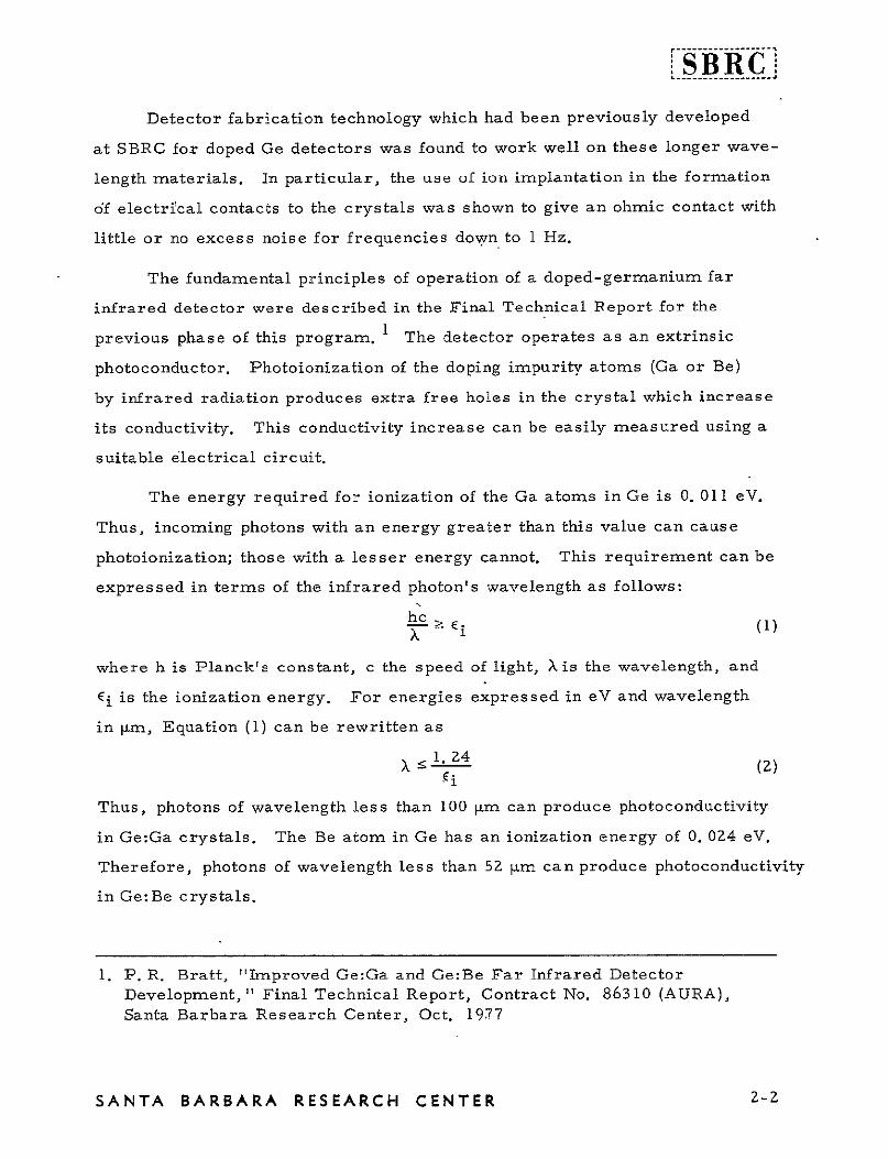
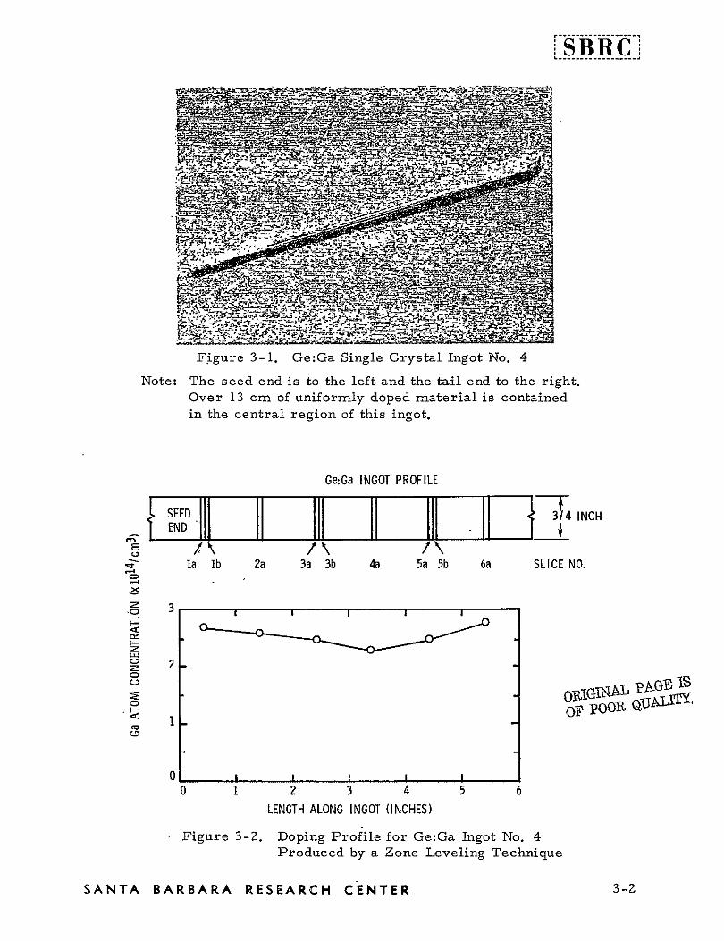
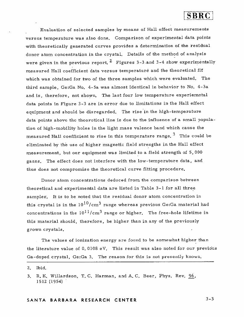
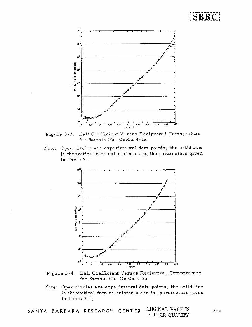
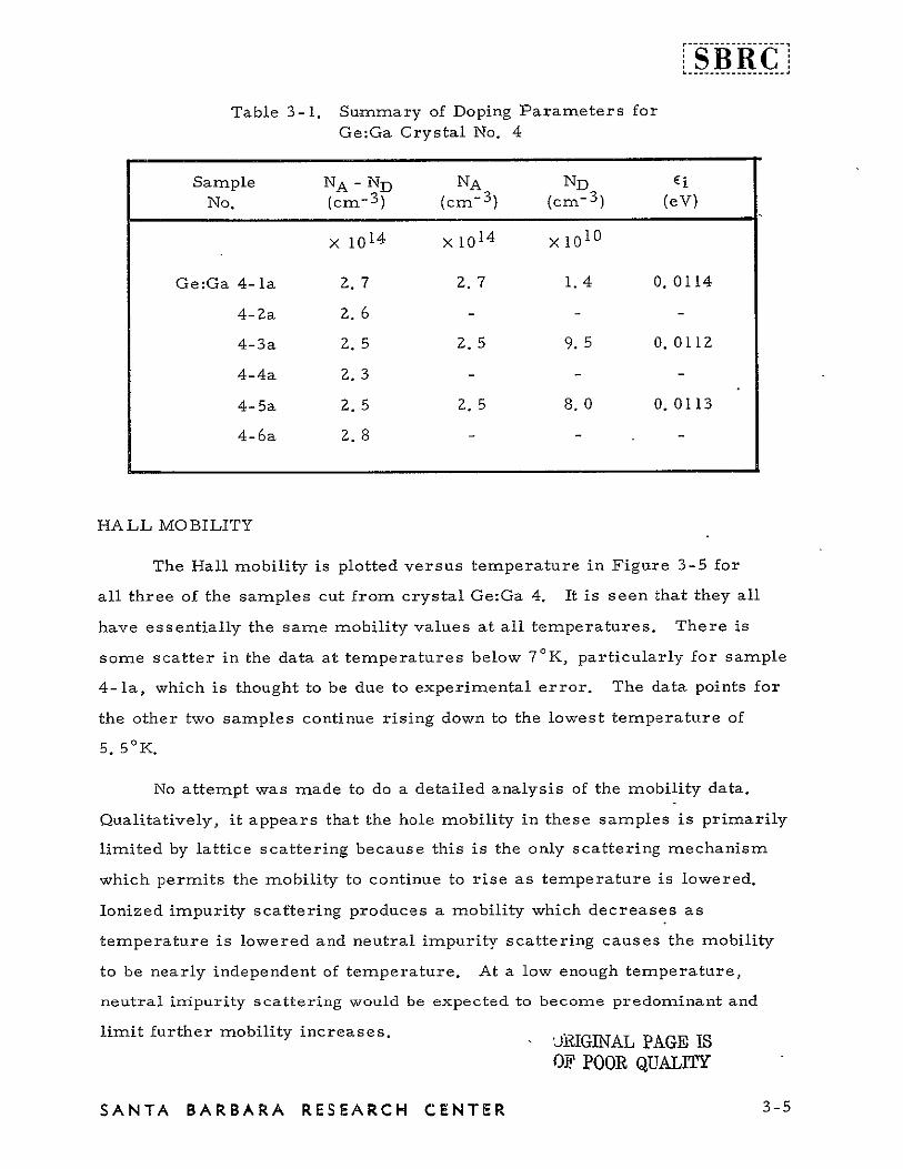
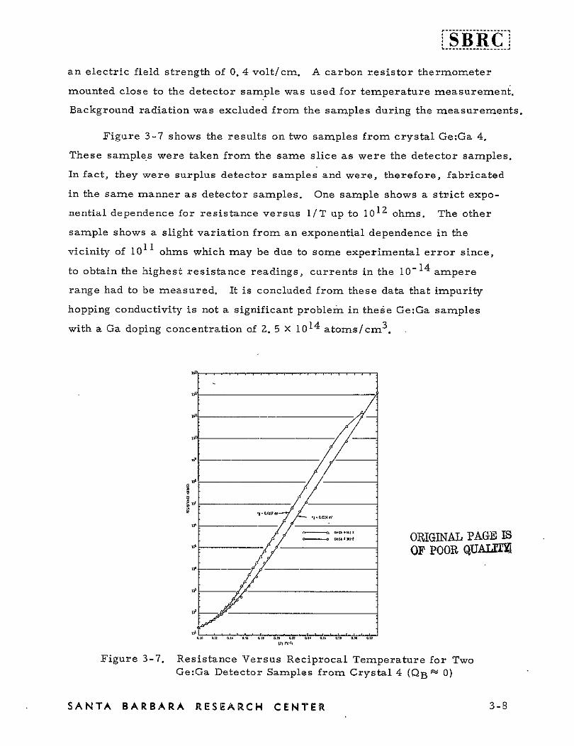
SBRC
Also to be noted in Figure 3-7 is the difference in resistance between
these two samples In the temperature range between 3 5 and 5K this
difference amounts to a factor between 5 and 6 Since both detector samples
were cut to the same dimensions and the hole mobility is the same in each
this implies a difference in the free-hole concentration of a factor between
5 and 6 In the temperature range of interest the free-hole concentration
is given by
ND iZrmkT exp (-EikT) (4)
where NA is the acceptor (Ga) concentration ND is the residual donor conshy
centration k is Boltzmanns constant h is Plancks constant Ei is the Ga
ionization energy and 6 is the ground state degeneracy of the Ga atom
Differences in free-hole concentration will be controlled by the acceptor
and donor doping concentration factor (NA - ND)ND From Table 3-1 using
values for NA and ND from slices 4-la and 4-5a (which were cut adjacent to
samples 4-lb and 4-5b) we calculate from this equation that the free-hole
concentration should differ by a factor of 6 Z and the sample with the lowest
ND value (4-lbl-2) will have the highest free-hole concentration and thereshy
fore the lowest resistance This is in good agreement with the measured
resistance data of Figure 3-7 These resistance data are -therefore confirmshy
ing evidence for the lower residual donor impurity concentration in the seed
end of GeGa crystal No 4
The ionization energies calculated from the slope of these resistance
versus lIT curves are in good agreement with the values obtained from Hall
coefficient data
SANTA BARBARA RESEARCH CENTER 3-9
-SBRC
Section 4
GeBe CRYSTAL GROWTH AND EVALUATION
GeBe CRYSTAL GROWTH
The initial GeBe crystals produced on this program were grown in
the same zone melting furnace used for GeGa crystal growth This furnace
was equipped with two doping spoons so that the doping alloy can be added to
the melt without opening the furnace to laboratory air Crystals were grown
in an atmosphere of hydrogen gas purified by passage through a hot palladium
membrane A GeBe doping alloy of approximately 0 01 atom percent was
prepared by meltfng together the appropriate amounts of high purity Ge and
Be in a quartz tube under hydrogen gas
In the first crystal growth run an amount of doping alloy was used
sufficient to produce about i015 Be atomscm 3 in the grown crystal The
calculation was based on a value for the distribution coefficient of Be in Ge
of 0 07 as reported by Shenker et al 5 It turned out that no Be was detected
by Hall effect measurements on the grown crystal Four more doping runs
were made with ever increasing additions of the Be doping alloy with essentially
the same result - no electrically active Be in the grown crystal Finally on
the sixth and seventh attempts using an exceptionally large amount of doping
alloy we were able to observe Be in the 1016 atomscm 3 range However
the concentration decreased rapidly in the direction along the crystal away
from where the doping pellets were placed and after about I inch no more
Be was detected
From these results it was concluded that Be must be going into the
crystal but most of it was being made electrically inactive by combining
with something probably oxygen The observation of an abnormal surface
5 H Shenker E M Swiggard and W J Moore Trans Metallurgical Soc
of AIME Z39 347 (1967)
SANTA BARBARA RESEARCH CENTER 4-1
--SBR
film on the top of the GeBe ingots was taken as possible evidence of BeO
which floats to the surface of the melt In addition Be atoms could be
complexed with oxygen in the bulk of the crystal This has been shown to
occur with boron-doped germanium 6
A check for Be and 0 in the bulk of the crystal was made using the mass
spectrographic analysis method Three samples were evaluated one from
crystal GeBe 5 and two from crystal GeBe 6 Crystal GeBe 5 showed no
electrically active Be in a Hall effect measurement Crystal GeBe 6 showed
electrically active Be in one sample (S-i) but essentially no Be in the other
The results of the mass spectrographic analyses are shown in Table 4-i
Because of interference from the 7 ZGe+ 8 line the detection of Be is someshy
what hampered However there is clear evidence of Be in sample GeBe
6-S-I The Hall effect measurement on this sample indicated 1 X10 1 6 atoms
cm 3 of electrically active Be which corresponds to 0 ZZ ppma The mass
spectrographic analysis indicates 65 ppma about 300 times the electrically
active amount There is also clear evidence of an ample supply of oxygen in
the crystal to complex with the Be Crystal GeBe 5 showed more than twice
the oxygen content of GeBe 6 Also of interest are the large concentrations
of the shallow acceptor atoms B and Al These concentrations are much
greater than would normally be detected in a Hall effect measurement and
indicate that oxygen complexing is also taking place with these atoms
From past work 7 8 it is known that oxygen is normally present in Ge
to a level of about 50 ppma although it has been noted 8 that the results will
vary depending on the method of crystal growth The mass spectrographic
analyses on our crystals showed much higher oxygen levels than normal
6 WD Edwards J Appl Phys 39 1784 (1968)
7 C D Thurmond W G Guldner and A L Beach J Electrochem Soc 103 603 (1956)
8 H A Papazian and S P Wolsky J AppI Phys Z7 1561 (1956)
SANTA BARBARA RESEARCH CENTER 4-Z
-SBRCI Table 4-i Impurity Concentrations in Three Germanium Samples
(in parts per million atomic ppma)
Detection GeBe 5 GeBe 6 GeBe 6Limit S-1 S-i S-2
Li 0 1 36 35 07 B 0 2 ND ND Z5 5 Be 10 0 20 0 65 0 10 0 O 03 1372 0 456 0 5650 Na 0 1 4Z 0 77 0 30 0 Mg 3 0 3 0 ND ND Al 0 7 35 0 91 5 23 0 Si 07 07 07 07 K 03 03 43 Z1 Ca 05 2Z 64 93 Cu 1 0 1 0 ND ND Ga 0 1 49 54 38 Ag 10 Z Z ND ND
Note Tantallum and gold are not reported since tantalum slits and gold foil are used Gallium is residual in the mass spectrometer Ge lines interfere with nitrogen and chlorine determination Other elements not detected have a detection limit of 5 ppma
Based on 1 X 10- 8 coulomb exposure
7 zGe + 8 interferes with Be determination The figures listed above are estimates based on the theoretical abundance ratio of Ge7Z to Ge74 isotopes (Measurements performed by Technology of Materials Santa Barbara California)
Because of the extensive zone refining done on the Ge before doping one
would have expected a lower oxygen content than normal From this result
a leak was suspected in the hydrogen purification system Indeed a leak
was found
Subsequent crystals were grown under vacuum with the objective
being to reduce the oxygen content in the melt by an out-gassing process
Three more crystals were grown during the remainder of this program
Crystal GeBe 8 was doped to Z X 1017 Be atomcm 3 using a single doping
SANTA BARBARA RESEARCH CENTER ORIGINALPAGEIS 4-3 OF POOR QUALITY
pellet addition at the seed end of the ingot Crystal GeBe 9 was incrementally
doped with Be to five different levels ranging from about 1 X 10¹⁴ to 7 X 10 1 5
Be atomscm 3 Figure 4-1 shows the doping profiles obtained for these two
ingots In both of these ingots the Be concentration indicated by the Hall
effect data was within 50 of the desired concentration Therefore it was
concluded that Be-O complexing was not a significant problem in these two
ingots To save time the starting Ge material used for these two ingots was
not extensively zone refined Only 3 to 5 zone passes were made on asshy
received intrinsic grade Ge
The last ingot grown GeBe 10 was subjected to extensive zone
refining before doping Some trouble was encountered with the doping spoons
however and the vacuum had to be broken to correct the problem The zone
heaters were turned off at this point After doping the measured electrically
active Be concentration was found to be significantly less than the desired
amount Therefore it was assumed that some Be-O complexing occurred
in this ingot Nevertheless a Be doping of about 1 X 10¹⁵ atomscm 3 was
achieved which was sufficient for detector fabrication and test
GeBe CRYSTAL EVALUATION
Preliminary evaluation of GeBe crystals was made by Hall effect
measurements at room temperature Since the Be atom is a double acceptor
in Ge with ionization energies of 0 024 and 0 064 eV each Be atom will
contribute two free holes at room temperature Thus the hole concentration
calculated from the measured Hall coefficient must be divided by two to
obtain the concentration of electrically active Be centers A magnetic field
strength of 15 kgauss was used in the room temperature Hall measurements
Examples of some of the results of these measurements were given in the
previous section
SANTA BARBARA RESEARCH CENTER 4-4
------shyLJ1SRC4 S B
INGOT PROFILE-II I I I I34 INCH
1 2 3 SLICE NO
X 2-
C-)
a
a I I
0 1 2 3 4 5
LENGTH ALONG INGOT (INCHES)
Be DOPANT PELLETS
2 3 4 5 SLICE NO
ji 10 III I
C
-6
C- 4a 3
2
0 i 2 3 4 5 6 LENGTH ALONG INGOT (INCHES)
Figure 4-1 Doping Profiles for Two GeBe Ingots
Note A ingot number 8 B ingot number 9 Black dots represent measured data points the dashed line is an approximate interpolation through the measured points
- ORIGINAL PAGE IS SANTA BARBARA RESEARCH CENTER OF POOR QUALTY 4-5
Selected GeBe samples were subjected to Hall effect measurements
versus temperature Analysis of these data provides additional information
on the crystal doping parameters such as concentration of shallow acceptor
impurities (probably B or Al) and compensating donor impurities A fourshy
level model was used to analyze the GeBe variable temperature Hall data
These levels are one shallow acceptor one shallow donor and the two Be
levels Based on this model theoretical Hall coefficient curves were genshy
erated and fit to the experimental data by adjusting the values of the various
dopant concentrations Further details of this analysis were presented in
the previous report 9
Figures 4-2 4-3 and 4-4 show examples of data obtained on GeBe
crystals 9 and 10 the solid line represents the theoretical fit to the data
points which are shown as crosses Table 4-Zgives the activation energies
and doping concentrations used to generate the theoretical curves In general
the fits to GeBe samples were not as good as those made to GeGa samples
This is undoubtedly due to the additional complexity of the four-level model
The value obtained for the Be concentration is quite accurate (plusmn 1-0) but
values for the shallow acceptor and shallow donor concentrations could
possibly be in error by as much as a factor of Z or 3 Nevertheless the
values obtained are useful for a rough comparison between different crystals
The shallow acceptor concentration was found to be on the order of
1 X 10¹³ atomscm 3 This is similar to what we have normally found in
undoped zone refined Ge The shallow donor concentration was quite low
in the 1010 to 1011 atomscm 3 range similar to what has previously been
observed in GeGa crystals
9 See Reference 1
SANTA BARBARA RESEARCH CENTER 4-6
SBRC i
1010
109
103
NBe
NSA
bull 65 x 10141cm3
52 x 10131cm 3
-
10c7
0
001 003 005 007 009 014 013 015 liT (1M)
Figure 4-Z Hall Coefficient Versus Reciprocal Temperature
for Sample No GeBe 9-Z
Note Crosses are experimental data points the solid line is theoretical
data calculated using the parameters listed in Table 4-2
101_
3 Nle 2 0 x 10151cm
3 o _ NSA 51 x 10131cm
0 19 NU - 2 8 x 101 cm3
108
04
0 04 006 00M 0 10 012 014 lIT (11XI
02
Figure 4-3 Hall Coefficient Versus Reciprocal Temperature
for Sample No GeBe 9-3
Note Crosses are experimentil data points the solid line is theoretical data calculated using the parameters listed in Table 4-2
SANTA BARBARA RESEARCH CENTER ORIGINAL PAGE IS 4-7
OF POOR QUALITY
SBRC
ilO 1010
01
N 109[NUe - 13 x 10151cm 3
i L NSA - amp2X 0121cm 3
0D 5 0 0 012 0 14
ill I
Figure 4-4 Hall Coefficient Versus Reciprocal Temperaturefor Sample No GeBe 10-3
Note Crosses are experimental data points the solid line is theoretical
data calculated using the parameters listed in Table 4-2
Table 4-2 Doping Parameters Obtained from Theoretical Fit of Four-Level Model to GeBe Hall Samples
SAMPLE NUMBER PARAMETER UNITS
9-2 03 70-3
0(Be) eV 00204 0102152 0214
e(Be2) eV 0 0568 00699 00643
e(SA) eV 00119 00142 00131 3 x i014N(Be) cm 647 196 x 1015 130 x 1015
-3 x i013 N(SA) cm 523 x i013 514 824 x 1012 N() cm -3 273 x loll 279 ix 250 x Z
C = IONIZATION ENERGY INeV -3N4 DOPING CONCENTRATION INcm
Be1 FIRST BeF ACCEPTOR LEVEL
Be2 = SECOND Be ACCEPTOR LEVEL OIINAL PAGE lBSA -SHALLOW ACCEPTORSR
D = SHALLOW DONORS
4-8SANTA BARBARA RESEARCH CENTER
-shy
The ionization energies obtained for the two Be acceptor levels are
reasonably close to the previously published values of 0 024 and 0 064 eV
The ionization energy obtained for the shallow acceptor is significantly
higher than the accepted literature value of 0 011 eV A similar result was
mentioned previously for the GeGa samples which were tested The reason
for this is not presently known
HALL MOBILITY
The Hall mobility measured on four Ge Be samples is shown in Figure
4-5 as a function of temperature The more lightly doped samples exhibit
a continually rising mobility down to the lowest temperature recorded The
sample with the heaviest doping shows a leveling off at a much lower mobility
This is due to neutral impurity scattering
The low-temperature mobility values of the samples with the lightest
doping (Nos 9-Z and 10-3) are comparable to those measured on the GeGa
samples and are still limited by lattice scattering even though the doping
concentration in the GeBe samples is 3 to 5 times greater This implies
that the neutral Be atom because of a smaller effective size in the Ge
lattice has a smaller scattering cross section
RESISTANCE VERSUS TEMPERATURE
A study of resistance versus temperature behavior was made on three
GeBe samples from crystal 9 and one from crystal 10 The purpose was to
check for hopping conductivity at temperatures below 4 ZK The measureshy
ments were made on surplus GeBe detector chips using the same circuit
arrangement that was used for the GeGa detectors (Figure 3-6) Backshy
ground radiation was excluded from the samples during these measurements
SANTA BARBARA RESEARCH CENTER 4-9
---
SBRCI
i d1 - - I dI _ I I4I
+ --
I1 FRI 1W1
jo I L
E -- -- 1+-
o GeBa 9-2 6 an-l4 II4 65 xTMIx J 0 GeBe 9-4 65 x 10154 0 k I [ ArGiB 9-3 xzGeBe91-3 130X 1015 -L--- i
I I
101 i1100 101 102 103
TEMPERATURE IM)
Figure 4-5 Hall Mobility Versus Temperature for Four GeBe Samples
The results are shown in Figure 4-6 The sample from crystal GeBe 9
with the least Be concentration shows no evidence of impurity hopping conshy
ducitivity As the Be concentration exceeds 1 X 10 15 atomscm 3 we see a
change in slope of the resistance curve at low temperature For the highest
doping concentration of 6 5 X 10 1 5 atomscm 3 a pronounced change in slope
is observed This is clear evidence of impurity hopping conductivity The
effect is to lower the sample resistance by roughly a factor of 50 in the lowshy
temperature range From these data it appears that the Be concentration in
the crystals should be kept below about Z X 10 1 5 atomscm 3 to avoid any
serious lowering of detector resistance due to hopping conductivity
L pAGBORIG OF pOOR QUJALtrt
SANTA BARBARA RESEARCH CENTER 4-10
to
11 G Be -2 t o ~ tot G U I 115
r 0 Irr I ee9 IG 1
R2 022 3z9 h I~ ~ ~ IT X-S1 3 11
Figure 4-6 Resistance Versus Reciprocal Temperature for Four
Uncompensated Ge Be Detectr Samples (QB 0)
The activation energy determined from the slope of the resistance
versus 1T curves is 0 0116 eV corresponding to that of a shallow acceptor
impurity This is to be expected because these Ge Be crystals are not
intentionally compensated with donor impurities Hall eff~ect data presented
in the previous section indicated a shallow acceptor concentration on the
order of 1013 atomscm 3 The hopping conductivity is due to electron
transfer between Be atoms however not between shallow acceptor levels
This obviously must be the case because the Be atom concentration exceeds
the shal low acceptor concentration by a factor of 650
SANTA BARBARA RESEARCH CENTER 4-11
[SB RC
IMPACT IONIZATION BREAKDOWN
Using the same test apparatus shown in Figure 3-6 measurements of
detector resistanc6 (or conductance) were made as a function of bias voltage
(or electric field strength) at two different temperatures The GeBe samples
used were the same four on which the resistance versus temperature measureshy
ments described inthe previous subsection were made Figures 4-7 and
4-8 show the resulting data plotted as conductance versus electric field
strength Figure 4-7 shows data taken at 4 2 0 K and Figure 4-8 shows data
taken at 3 45 0 K (with the exception of sample GeBe 9r4a which was run at
3 00 K)
These curves show a rather complex behavior however they can be
understood in a qualitative way Ohmic conduction occurs only at very low
electric field strengths less than 1 voltcm (This is not immediately
evident with the scale which was chosen for electric field strength but was
observed) As the electric field is increased the sample conductance
increases due to impact ionization of the shallow acceptor levels At 4 20 K
the three samples GeBe 9-2a 10-3a and 9-3a show this in a very proshy
nounced way The other sample GeBe 9-4a does not show this effect so
much because it is dominated by impurity hopping conduction At some
relatively high value of electric field strength impact ionization of the Be
atoms commences and the conductance rises very sharply as indicated by
the upward pointing arrows Sample GeBe 9-Za could not be biased to the
point of impact ionization of the Be atoms because of sample heating which
occurred due to its higher conductance At a 45 0 K a similar behavior is
noted although the shapes of the curves are altered from what they are at
4 2 0 K Also to be noted is the increase in the critical field strength for
impact ionization of the Be atoms when the temperature is lowered from
4 Z0 to 3450K
SANTA BARBARA RESEARCH CENTER 4-1Z
i SBR
-10-]
IV
0 G9e 92a 65bull1014
G Be 9-U 2 0 1015
oC81B9-a 65e 1015 +
lO bull G8 10-3n 1 3 1015
ELETRI FIL STENT N ru3
I
Ge Be Detector Samples at 420 K (QE 0)
n-5
t IAto~l 1
0 Gege 9-4n 67 1014
IOL0 x UeBe9-4e 6 5 1015
10 I
0 v4 0 it I00 IdDELECTRIC STRENGTH GIEMFIELD
Figure 4-8 Conductance Versus Electric Field Strength for GeBe Detector Samples at 345degK (QB 0)
SANTA BARBARA RESEARCH CENTEtR 4-13
Section 5
DETECTOR FABRICATION AND TEST
DETECTOR FABRICATION
Detector chips were cut from the GeGa or GeBe crystals and fabricated
into detector elements using standard processing technology which was
previously developed at SBRC Electrical contacts to the detector were formed
by ion implantation of boron ions This produces a p+-p contact with uniform p+ doping and a highly planar interface with the p-type crystal bulk Each
detector element was assembled onto a tungsten metal mount along with a
load resistor and cryogenic preamplifier This assembly is shown in
Figure 5-1 The load resistor had a nominal value of 5 X 10¹⁰ ohms at 3degK
The MOSFET was a Hughes W164 p-channel enhancement mode device
All GeGa detectors fabricated during this phase of the work were cut
from crystal GeGa 4 However each of the three detectors was made from
a different slice so that an evaluation of the whole ingot would be obtained
Detectors were made from slice numbers Ib 3b and 5b Figure 3-2 showed
the location of these slices in the ingot The Ga doping concentration in the
detectors was Z 5 X 10¹⁴ atomscm 3 All GeBe detectors fabricated were
from the same slice of crystal GeBe 10 The Be concentration in the
detectors was 1 3 X 10¹⁵ atomscm 3
LOW BACKGROUND TEST DEWARS
The detector assemblies were mounted to a two-part cooper heat sink
which was designed to provide a vise-like clamping of the tungsten detector
mount to the copper heat sink This design was chosen to obtain good thermal
conduction to the detector mount A carbon resistor thermometer was imshy
bedded in a hole drilled into the copper heat sink Figure 5-2 shows a
sketch of the heat sink design
SANTA BARBARA RESEARCH CENTER 5-1
J -cmma1c
DRAINTI JA
LOAN
SUBSTRT 0GATEJ
Figure 5-1 Detector - Cryogenic Preamplifier Assembly
ORIGEt PGE
Mounting Detector-Figure 5-2 Sketch of Copper Heat Sink for Preamplifier Assemblies to the Low-Background
SANTA BARBARA RESEARCH CENTER 5-2
LISBRC
This copper heat sink was mounted in a Janis Model RD liquid helium
dewar An aperture defining the sensitive area (-mm X Q- mm) of the
detector was placed directly over the detector and a baffle plate with Z0 mm
diameter aperture was placed directly over that This configuration was
used in an effort to prevent stray radiation from getting to the sides of the
detector A series of aperture plates and cold filters were located between
the detector and the dewar outer window to provide the desired attenuation of
background radiation Figures 5-3 and 5-4 show the filtering arrangements
used in testing GeGa and GeBe detectors Two separate dewars were used
to avoid having to take apart the filtering assemblies and thereby possibly
cause an irreproducible change in the test set up
The background photon flux density arriving at the detector plane was
calculated from the following formula
QB (AX)= Q (300 0 KAX) TRsinZz (5)
where Q(300 0 K AX) = photon irradiance from Zir sterradians of 300K blackbody radiation integrated over the filter pass-band
TR = total peak transmittance of all filters
S = detector field-of-view angle defined by aperture and distance from detector to aperture
The details of this calculation for the different low-background conditions used
in detector evaluation are presented in Appendix A
For GeGa the cold filtering consisted of two special black polyethylene
filters and two neutral density filters The special black polyethylene l 0 acts
as a long-pass filter with a cut-on wavelength of about 80 gim It is a scattershy
ing filter made by mixing various alkali halide crystal powders together with
polyethylene and hot rolling them into a thin film Some carbon particles
also may be in the mixture The true constituents in the film are not known
10 We are grateful to K Shivanandan of NRL for supplying us with this filter material and its relative spectral transmittance curve
SANTA BARBARA RESEARCH CENTER 5-3
SBRC
-_LIQUID NIT(ROGEN LIQU ID-HEL IUM
DETECTOR IPREAMP
BAFFLE PLATE WITHbullram DIAME~TER L -ASSEMBLY
APERTURE AREA DEFINING APERTURE
1mm DIAMETER --- -INSIDE WALLS
FOV APERTURE BLACKENED WITH 3M BLACK VELVET
NEUTRAL DENSITY 7 SPECIAL POLYETHYLENE FILTERS IBOpmCUT-ON)
FILTER
u _ CRYSTAL QUARTZ
BILACKBODY SOURCE (5OOdegK)
CHOPPER MOTOR
Figure 5-3 Low-Temperature Low-Background Dewar Setup for Testing of GeGa Detectors at 100 jim
LIQUID NITROGEN LIQUID HELIUM
DETECTORPREAMP
ASSEMBLYBAFFLE PLATE WITH 2-rm DIAMETER AREA DEFINING APERTURE APERTURE
-mm DIAMETER INS IDEWAL FOV APERTURE BLACKENED WITH
3M BLACK VELVET
NEUTRAL 16- TO 22Nm ORIGINAL PAGE IS DEN4SIT FITR-ooVA FILTER KRS-5 OF POOR
dBLACKBODYSOURCE (SOK)
CHOPPERMOTOR
Figure 5-4 Low-Temperature Low-Background Dewar Setup for Testing of GeBe Detectors
5-4SANTA BARBARA RESEARCH CENTER
SBRC to us The neutral density filters were made at SBRC by evaporating a thinshy
nichrome metal film onto z-cut crystal quartz flats The relative spectral
transmittance of these filters was not measured but was assumed to be
essentially flat in the 60- to IZ0-gLm range The average transmittance of
these filters was checked at room temperature by placing each filter in
front of a dewar containing a GeGa detector (also filtered to detect only
radiation beyond about 60 4m) and measuring the attenuation of the detector
signal from the 500 0 K blackbody source
In most of the GeGa detector testing done on this program a filter
combination was used which gave a calculated background flux QB = I 2 X 10⁹
photonscm 2 sec at the detector plane Measurements on one detector were
made at other background flux levels which were obtained by changing the
neutral density filters and field-of-view (FOV) aperture
For GeBe detector testing a combination of a 16- to 22-gm multilayer
interference band-pass filter I and two neutral density filters was used In
this case the neutral density filters were made by evaporating nichrome
metal onto germanium flats This filtering combination had worked well for
testing doped Si detectors in past work at SBRC and was easy to implement
for the GeBe detectors Admittedly it would be more desirable to test
these detectors in the 30- to 50-4m range however a suitable combination
of filters for this range was not readily available so the 16- to ZZ-gm range
was used instead Extrapolation of NEP data from the 16- to 22-grn range
to 50 jim can be made with little additional expected error The filter comshy
bination used for GeBe detector testing gave a calculated background photon
flux at the detector of QB = 9 X 10⁸ photonscm 2 sec
11 Obtained from Optical Coating Laboratories Inc
SANTA BARBARA RESEARCH CENTER 5-5
-SBRC The signal radiation was obtained from a 500K blackbody located in
close proximity to the dewar outer window A variable speed chopped proshy
vided modulation frequencies from 1 to 1000 Hz The blackbody has a large
opening and the detector looks into this opening through the small FOV
defining aperture located within the dewar Therefore the blackbody radiashy
tion is effectively emanating from this aperture rather than from the blackshy
body cavity itself The blackbody signal irradiance at the detector plane
is given by the formula
HBB (AX) = WBB(AX) ABB TRF (6)Tr DZ
where WBB(AX) = blackbody radiant emittance integrated over filter passband
ABB = FOV defining aperture area
TR = total filter transmittance
F = chopper form factor
D = aperture to detector distance
The signal irradiance on the detector is due to the temperature difference
between the 500 0 K blackbody cavity and the room temperature chopper blade
(assumed to be at 300 0 K) Therefore the signal photon flux density impinging
on the detector is greater than the 300K background photon flux density For
noise measurements the blackbody opening is covered with a shutter so that
the detector then only sees 300K background photons
The blackbody radiant emittance was numerically integrated over the
filter pass-band to obtain that fraction WBB(AX) which would pass through
the filter The details of this calculation are given in Appendix B
The chopper form factor is used to convert peak-to-peak signal
irradiance values to root-mean-square values For the chopper used this
factor had a value of 0 40 A listing of all the parameter values used in
Equations (5) and (6) are given in Table 5-1
SANTA BARBARA RESEARCH CENTER 5-6
Table 5-1 List of Parameters Used in Blackbody Irradiance Calculations
Parameter Units GeGa Ge Be
WBB(AX) wcm Z 3 29 X 10-4 1 53 X 10- Z
-3 - 3ABB cmZ 7 85 x i0 1 96 X 10
TR 181 X 10- 4 1 0 X 10- 4
D cm 8 59 6 65
F 040 040 - IZHBB(AX) w(rms)cm2 8 05 X I0- 13 8 6 x 10
o degrees 067 043
QB(3000 AX) photonssec cmz 149 X 1017 636 x 1017
QB(AX) photonssec cmz 1 Z X i09 0 9 X 10⁹
TEST PROCEDURE
All testing was done in a screen room Tests were performed using a
source follower cryogenic preamplifier and the external circuit components
shown in Figure 5-5 The preamplifier output was coupled to a Quan Tech
Model 206C amplifier which provided a voltage gain of 103 Amplifier
frequency response was flat between IHz and 100 kHz The low-frequency
gain was -3 db at 05 Hz Signal and noise readings were taken on a Quan
Tech Model 304 Wave Analyzer and also visually monitored on an oscilloscope
Tests were designed with the object of evaluating detector performance
as a function of frequency voltage and temperature Data were taken at
0 50 K increments from about 4 50 K down to Z00 K Temperatures below
4 ZK were obtained by pumping over the liquid helium reservoir of the Janis
Dewar A calibrated carbon resistance thermometer mounted in a hole
drilled into the copper heat sink shown in Figure 5-Z was used to monitor
detector temperature
ORIGINAL PAGE IS
SANTA BARBARA RESEARCH CENTER OF POOR QUALITYl 5-7
LsBRCJ S DRAIN
lLOAD ---
RESISTORI I l
QUAN TECHWAVE
IANALYZER
IL I DETECTOR C_ _26~ t MFIER-LOSCILLOSCOPE
SOURCE RES ISTOR
Figure 5-5 Diagram of Circuit Used for GeGa and GeBe Detector Tests
Note Circuit elements within dashed line are at cold temperature those outside are at room temperature
Detector bias was first optimized at the highest operating temperature
which gave a reasonable signal-to-noise (SIN) ratio This was usually
around 4 00 K The temperature was then reduced in 0 5 0 increments At
each new temperature setting signal noise and resistance measurements
were taken at 10 Hz with optimum bias At 3 0degK and 00 K a more detailed
look at detector performance was made At these temperatures the measureshy
ments made were 1) zero bias noise versus frequency Z) signal and noise
versus bias at 10 Hz and 3) signal and noise versus frequency at optimum
bias
RESULTS - GeGa DETECTORS
Three GeGa detectors were fabricated and tested during this program
All were made with material from crystal GeGa 4 Detector 4-lbl-1 showed
optimum SN ratio when operated at a bias voltage of 0 035 volt (0 7 voltcm)
while detectors 4-3b1-i and 4-5bl-I had an optimum bias of 0 0Z4 volt
SANTA BARBARA RESEARCH CENTER 5-8
SBRC
(0 5 voltcm) Detectors 4-lbl-l and 4-361-1 were tested only at one
background flux level namely 1 Z X 10 9 photonsseccm Z Detector 4-5bl-l
was tested at various different background flux levels Figures 5-6 through
5-13 illustrate the relationship between bias voltage resistance signal
noise and NEP of these detectors
The resistance versus temperature data in Figure 5-6 show the same
characteristics as were seen earlier in Figure 3-7 That is detector
4-lbl-l has a lower resistance at any given temperature than either 4-3b1-i
or 4-5bl-i This is due to a lower concentration of compensating donor
impurities in this part of the crystal
Detector 4-5b1-l shows an increase in resistance with decreasing
background flux however the magnitude of this increase is less than expected
Since QB was decreased by a factor of 3 2 detector resistance should have
increased by this factor Instead it only increased by a factor of 1 6 From
this result it might be inferred that the calculated background flux level of
3 7 X 10 8 photonsseccm 2 was in error This could possibly have been the
case However it also should be pointed out that there can be a substantial
error in the resistance measurements reported in Figure 5-6 These are
made by an indirect method through the source follower MOSFET circuit
Appendix B describes this method Also the temperature measurements
could be in error due to the fact that the temperature sensing resistor is not
located on the detector but is some distance away in the copper heat sink
Figure 5-7 shows the detector behavior as a function of bias voltage at
two different temperatures Z 0 and 3 00 K Note that at 3 00 the signal
voltage tends to saturate at higher bias This could be caused by either of
two things 1) the drop in detector ac resistance as bias voltage is increased
or 2) photoconductive gain saturation due to carrier sweep-out Signal
saturation was not observed at 2 00 K operation Similar results were found
on two of the three GeGa detectors tested a tendency toward signal saturashy
tion at 3 0degK but no such tendency at 2 0degK This indicates a much lower
free-hole lifetime at 2 00 K operation
SANTA BARBARA RESEARCH CENTER 5-9
------------
a - p
ol
4-3b-I Q bull 12 x109phsC 2m-2
l4-Tbl-L Q8 - 12x 109 ph sc Cmn2
24-5b1-L Q8 37 x108phsec-I cm 9 1144b11 Oi3 seIDSb-O~-12xI I phsC mm
20 25 30 35 40 45 DETECTOR IMTEMPERATURE
Figure 5-6 Resistance Versus Temperature for GeGa Detectors
SIGNAL 1O-
4 loll
010--5- 10
2 A RESISTANCE -~
E
I~NOISE
10-6-0 9
ORIGINAL PAGE IS
NIPN0 OF POOR QALITY
~2degK 3degK
001 00 a 0 D4o 0w 04060 awo DETECTOR tolts)VOLTAGE
Figure 5-7 Signal Noise NEP and DC Resistance Versus Bias Voltage for GeGa Detector No 4-lbl-l at Two Temperatures (10 Hz Data)
SANTA BARBARA RESEARCH CENTER 5-10
The detector resistance decreases with increased bias This is due
primarily to an increase in free carrier density because of an increasing
lifetime with bias
The noise voltage at low bias is predominantly preamplifier noise As
bias voltage is increased detector noise becomes evident
The NEP is higher at low bias voltage because of the preamplifier
contribution to the noise At higher bias it tends to level off This is
typical of most GeGa detectors that have been tested Some however
have shown a clear minimum and then an increasing NEP at higher bias
probably due to an excess detector noise arising at the detector contacts
The detector signal data in Figures 5-8 and 5-9 can be used to calculate
detector responsivity values and from these one can obtain estimates of
quantum efficiency and photoconductive gain The voltage responsivity at
wavelength X is a function of frequency due to the circuit RC rolloff This
frequency dependence can be written as I
Rv(Xf) = Rv(X o) [1 + (ZlfTRRc)Z] - 2 (7)
where Rv(X o) is the dc or low-frequency responsivity and TRC is the circuit
response time By fitting a curve having the functional dependence on
frequency shown by this equation to the signal data in Figures 5-8 and 5-9
it was found that the 1-Hz responsivity values are sufficiently close to the
dc value to be used in an approximate calculation The 1-Hz voltage responshy
sivity was calculated from experimentally measured data using the formula
RVXI)- S (AX) (8)Rv(X 1) = HBB(AnX)ADg
where S(AX) = signal voltage measured at output of preamplifier
HBB(AX) = blackbody irradiance at detector (see Table 5-1) 3
AD = detector area (7 5 X 10 - cm 2 )
g = preamplifier gain (0 85)
SANTA BARBARA RESEARCH CENTER 5-11
4-lbl- 4-3b1-1 4-5b1-l
10-3
- SIGNAL
04
10-5
-6
NOISE
PREAMPLIFIER
8 l10 - i i i l
1 10 100 1000
FREQUENCY (Hz) Figure 5-8 Signal and Noise Versus Frequency for GeGa
Detectors at 3 00 K
Note Background photon flux density was 1 2 X 10⁹ ph sec - I cm - Z
Signal and noise values are referred to the output of the MOSFET preamplifier
SANTA BARBARA RESEARCH CENTER 5-1Z
SBRCI ----- 1--T-T- -r---------TT--------T-shy
10 _
o 10-5
SIGNAL
0 2
10- 7 PREAMPLIFIER
NOISE
4-1bl-1 QB = 12 x 109 ph sec - I cm -shy 4-3b1-1 QB = 12 x 109 ph se-C mshy2
4-5b1-1 QB = 12 x 109 ph sec - I cm- 2
10_8 4-5b1-1 QB = 37 x 108 ph sec - 1 cm shy 2
1 10 100 1000 FREQUENCY (Hz)
Figure 5-9 Signal and Noise Versus Frequency for GeGa Detectors at Z 00 K
Note Background photon flux density was 1 Z X 10 9 ph sec-I cm-Z Signal and noise values are referred to the output of the MOSFET preamplifier
SANTA BARBARA RESEARCH CENTER 5-13
-SB -RC
The short-circuit current responsivity was calculated from the voltage
responsivity using the equation
is(X 1) = Rv(X 1)R (9)11
where R11 is the parallel resistance formed by the load and the detector ac
resistance values
RacRLH11 = Rac + RL (10)
and
[ V dRdc-Rac = Rdc l - - (11)I Rdc dV
According to detector theory the short-circuit current responsivity is given
by
w e= c GP c (lZ)
Lc = photoconductive gain
7 = free-hole lifetime
S= hole mobility
E = electric field strength
L = interelectrode spacing
77 = quantum efficiency
e = electronic charge
X = wavelength
h = Plancks constant
c = speed of light
Therefore once a value for I(X o) is obtained some estimates of values for
17 and Gpc can be made
Using the foregoing equations and the measured experimental data
values of current responsivity were calculated for the three GeGa detectors
The results for operating temperatures of both 2 0 K and 3 00 K are shown
in Table 5-Z The current responsivity values are at the peak of the detectors
SANTA BARBARA RESEARCH CENTER 5-14
i-SBRCj]
Table 5-Z Parameters Used in Calculation of Short-Circuit
Current Responsivity for GeGa Detectors
DETECTOR NUMBER TEMPERATURE PARAMETER UNITS 4 (OK)
4-]b1-1 4-3b1-1 4-5b1-1
BIAS VOLTAGE VOLTS 0035 0024 0024 20 AND 30 ELECTRIC FIELD VOLTSICM 070 048 048 20 AND 30
10 x I010 Rdc OHMS 5 K 109 14 x 10I0 30
Rac OHMS 28x 109 73 x 109 Li x 1010 30
S(AX 1) MILLIVOLTS 044 020 019 30
RV(Ap 1) VOLTSIWATT 86 x i010 39 X 1010 37 x 1010 30
Is(p 1) AMPS WATT 32 (10) 61 41 30
nGpc (0124) 0076 0051 30
Rdc OHMS 16 x 1010 20 x 1010 31 x 1010 20
Rac OHMS 12 x 1010 13 X 1010 24 x 1010 20
S(441) MILLIVOLTS 023 012 015 20
x 1010 Rv(Xpl) VOLTSWATr 4 5 X 10¹⁰ 23 29 x 1010 20
Is(Ap 1) AMPSWAnT 46 22 18 20
flGpc 0057 0021 0022 20
RL - 5 x 10¹⁰ (NOMINAL VALUE)
Xp = 100 Pm 0hAT VAGE IS
AD - 7 5 x 10⁻³ cm2 (15 x 05 mm) ORUGNL- ALI OF pOOR Q
f =IHz
pm An exceptionallyspectral response curve which was taken to be 100
0 high value of current responsivity was obtained for detector 4-lbl-l at 3 O K
No obvious experimental error could be found in the data however the result
does seem to be spurious By comparison of the Z 00 and 3 00 K current
value around 10responsivities of the other two detectors it appears that a
ampswatt would be more appropriate for this detector The current
responsivity for this detector would be expected to be somewhat higher than
the others because of a higher applied bias and longer free carrier lifetime
Both ofthese conditions lead to a higher photoconductive gain for this detector
The signal versus bias voltage data shown previously in Figure 5-7 indicate
that the photoconductive gain could be on the order of 0 5 (This result is
of course based on the assumption that the maximum value of the gain at
saturation is 0 5 ) The use of these results in Equation (12) leads to a
5-15SANTA -BARBARA RESEARCH CENTER
quantum efficiency of 0 Z5 which seems reasonable considering the Ga doping
concentration used in these detectors The other two detectors probably are
operating with a photoconductive gain around 0 Z at 3 O0 K For Z 00 K
operation a decrease in current responsivity by a factor about 2 5 is
observed This must be attributed to a decreased photoconductive gain of
the same amount since the quantum efficiency would not be expected to
change simply because of a change in operating temperature
The measured signal-and-noise data was used to calculate the NEP
data which is shown in Figures 5-10 5-11 and 5-1Z The NEP versus
frequency data shows an essentially flat behavior from 1 to 40 Hz and then
rises slowly An effort was made to measure detector noise data at frequencies
below 1 Hz using a spectrum analyzer The data obtained were unreliable
thus not reported here
The NE versus temperature data of Figure 5-12 show a fairly clear
minimum at 3 00 K operation At higher temperatures NEP increases due to
increasing detector generation-recombination noise and decreasing detector
resistance At lower temperatures the NEPincrease is mainly due to a
decreased detector responsivity The conclusion is that the optimum operatshy
ing temperature is close to 3 00OK NEP values of about 0 7 to 1 X 10-16 1
wattsHz2 were achieved with a background flux of 1 2 X 10⁹ photonsseccm Z
One detector number GeGa 4-5b-i was also measured at various
different background flux levels Figure 5-13 shows a plot of calculated NEP
values versus frequency at four different flux levels At the highest backshy
ground flux NEP rises in the low-frequency range This is due to 1f noise
in the detector At the lower background flux levels NEP shows less
dependence on frequency and is reasonably flat down to 1 Hz - The lowest1
-measured NEP was 4 X 10 - 1 7 wattsHz at I -lz with a background level of
3 7 x 10 8 photonsseccm z
SANTA BARBARA RESEARCH CENTER 5-16
10-15 iI iF ---- I~t T--
T4-lbl-1 QB 12 x 109-E s---f1j2 -I -2
4-3b1-1 QB = 12 x 109 ph sec cm 1 -2
4-5b1-1 QB = L2 x 109 ph sec- cm
QB -37 x 108 ph sec- cm -2 4-5b1-I
1 1 4 - - --- o
1 0 -17 [ 1 1 1 1 1 I1 1 1 II I
1I0 100 1000
FREQUENCY (Hz)
Figure 5-10 NEF Versus Frequency for GeGa Detectors at 3 OdegK
10-1
I -2 4-Ibi-1 QB - 12 x 109 ph sec cm
I -2 4-3bl-1 QB = 12 x 109 ph sec cm
I 24-5bl-1 Q8 12 x 109 ph sec Cm
- 2 4-56l1-I 37 x 108 phsec 1 cmQB shy
__ 1
iiiI fl LLII I it
1 10 100 1000
FREQUENCY (Hz)
Figure 5-11 NEP Versus Frequency for GeGa Detectors at Z00 K
SANTA BARBARA RESEARCH CENTER 5-17
iSBRC]
4-1E- OB 1]2 x ]09 ph sle c 2
4-31-L Q8 L2 X109ph se-t cm-2 4-b1-1 QB - 12 x 109 phse 1 cm 2
4-5b1-L QBshy3 7 X10⁸ ph seC1 cm -2
t
I IT
-----I
1WI71
20 25 30 3r5 4 0 4 5
TEMPERATURE(K1
Figure 5-1Z NEP Versus Temperature for GeGa Detectors at a Frequency of 10 Hz
SQB- 124 x 109 phseccm2
QR 3 7 x 10⁸ phlseclcm2
Q8 = 175 x 1010 phlseccm 2
BQ 117 x j112 phseclcm2
10_14 _________ ________ _______
- NOTE SCALE CHANGE
S --shy _-shy
1 10 100 1000
FREQUENCY (Hz)
Figure 5-13 NEP Versus Frequency for GeGa Detector 4-5b-I at 3 00 K for Four Different
Background Flux Levels
SANTA BARBARA RESEARCH CENTER 5-18
r ---------------SBRC
RESULTS - GeBe DETECTORS
As mentioned previously all three GeBe detectors fabricated and
tested on this program were cut from the same slice of crystal Ge Be 10
The slice number was 3a and the location of this slice in the crystal was
adjacent to slice 3 from which the Hall sample was taken The Be doping
1 3 X 10 1 5 concentration was atomscm 3 Figures 5-14 through 5-Z0
illustrate the relationship between bias voltage resistance signal noise
and NEP of these detectors lt
In Figure 5-14 the signal is seen to be a linear function of bias voltage
and does not tend to saturate as did the GeGa detectors The resistance is
seen to be nearly constant with bias voltage to it can be assumed that Rac
is equal to Rdc The NEP is higher at low bias due to preamplifier noise
and then decreases tending to flatten out as bias increases This is quite
evident at Z 00 K operation but for this particular detector at 3 00 K the
NEP starts rising prematurely due to excess detector noise The other
detectors tested showed the flatter NEP curve at both operating temperatures
Figure 5-15 shows the measured resistance versus temperature data
The detectors all have similar resistance values as would be expected for
detectors cut from the same slice of material Since this material did not
show significant hopping conductivity the resistance is background photon
limited at the lowest temperatures with a value of Z 5 X 10 1 0 ohms This
resistance value is substantially lower than might be expected based on a
theoretical calculation The background limited dc resistance can be
expressed as
Rdc - L cflQBTepiw
(13)
ORIGINAL PAGE IS OF POOR QUALITY
SANTA BARBARA RESEARCH CENTER 5-19
--- S- --- -shy
- ~ SIGIAL
---20K
i0 5 IOU
6I0- -1-
NOISE RESISTANCE
Detector Voltage for CeBe l0-3a-3 at TwoTemperatues 2degK and 3K
-10-33-1 10-3a-2
010-ashy
109
20 2 303540 45s DETECTOR (KT5MPERATURE
Figure 5-15 Resistance Versus Detector Temperature of Ge Be Detectors
Note Background photon flux density was 0 9 X 10 9 ph sec-1 cm-2
SANTA BARBARA RESEARCH CENTER 5-Z0
LSBRC
Inserting the following values into this equation
- ZL = 5 X 10 cm
T7 =03
QB = 9 X 10⁸ photonsseccm Z
i =10 - 7 sec
e = 16 Xl0- 1 9 coul
ii = 4 X 10⁵ crZvolt sec
w = 1 5 y0-1 cm
gives a value for Rdc of 1 9 X i01 ohms nearly an order of magnitude
higher than measured All the above parameters except 71 QB and T came
from direct measurements The 77and T values are reasonable approximations
which should be within a factor of 2 or 3 of the true values It would be
necessary to increase the 77 product by a factor of 10 to bring the calculated
Rdc into agreement with the measured value This seems to be unreasonable
therefore it must be concluded that QB is actually higher than the stated
value of 9 X 10⁸ photonsseccm z
Figures 5-16 and 5-17 show measured signal-and-noise data versus
frequency for two operating temperatures The signal data can be analyzed
in the same way as for the GeGa detectors to obtain short-circuit current
responsivity values and estimates of the 1]Gpc product The results are given
in Table 5-3 The blackbody signal radiation was restricted to the 16- to
22-gim band by a filter Therefore direct use of Equation (8) gives the
voltage responsivity at a wavelength of -about 19 pLm To convert this value
to responsivity at the peak of the GeBe spectral response which is at 40 pLm
the calculated responsivity was multiplied by a factor of 2 This factor is
based on the relative spectral response of GeBe reported by Shenker et al 12
All the values of voltage and current responsivity listed in Table 5-3 are at
the detectors peak wavelength of 40 pLm The calculated current responsivity
values are seen to be in the neighborhood of 2-5 ampwatt DetectorGeBe 10-3a-3
1Z See Reference 5
SANTA BARBARA RESEARCH CENTER 5-21
tllm I - r rt irn I ITII41
10-3a-1 10-3a-2 10-3a-3
10-3 N
SIGNAL
10shy4
J4______
-
C
10-5
CNOISE
PREAMPLIFIER NOISE 10-7 shy
-RIGINAL PAGE IS OF POOR QUALTY
1 10 100 1000 FREQUENCY (Hz)
Figure 5-16 Signal and Noise Versus Frequency for GeBe Detectors at 3 00 K
Note Background photon flux density was 0 9 X 1-09 ph sec- 1 cm-Z Signal and noise values are referred to the output of -the MOSFET preamplifier
5-ZZSANTA BARBARA RESEARCH CENTER
l II IIIII~~~SR
-L1B3ashy
10-3a-1 - ------10-3a-2 --- 10-3a-3
10- 41______ __
10-4
a V SIGNAL
-shy4
PREAMPLIF IERNOS
- 810 1 a I l i l t I J l
1I0 100 1000
FREQUENCY (Hz)
Figure 5-17 Signal and Noise Versus Frequency for GeBe Detectors at 2 OdegK
Note Background photon flux density was 0 9 X 10 9 ph sec-i crn-Z
Signal and noise values are referred to the output of the
MOSFET preamplifier
SANTA BARBARA RESEARCH CENTER 5-23
SBRC L -
Table 5-3 Parameters Used-in Calculation of Short-Circuit Current Responsivity for GeBe Detectors
UN ITS DETECTOR NUMBER TEMPERATUREPARAMETER 10-3a-3 (OK)10-3a-1 1O-3n-2
BIAS VOLTAGE VOLTS 0235 0235 0082 30 ELECTRIC FIELD VOLTSICM 470 470 164 30
Rac OHMS 19 x 1010 22 x 1010 18 x 1010 30 S(AX 1) MILLIVOLTS 18 19 056 30
Rv(Xp 1) VOLTS(WAT 66 x 1010 69 x 1010 20 x 1010 30
Is(Xp 1) AMPSWAIT 57 54 18 30
flGpc 0176 0167 0056 30
BIAS VOLTAGE VOLTS 0259 0353 0188 20
ELECTRIC FIELD VOLTSICM 519 705 376 20
Rac OHMS 22 x 1010 26 x 1010 27 x 1010 20
S(AX 1) MILLIVOLTS 15 11 11 20
Rv(Ar 1) VOLTSIWAIT 55 x 1010 40 x1010 40 x 1010 20
Is(Xp 1) AMPSIWATT 43 29 28 20
1GPC 0133 0090 0081 20
RL =3 x 10¹⁰ OHMS (NOMINAL VALUE)
Ap = 40 pm AD 75 x 10-3 cm2 15 x 05 mm)
I =1 Hz
was somewhat lower than the other two because it had to be operated at a
lower bias voltage If one assumes a quantum efficiency of 0 3 then the
photoconductive gains would be in the range of 0 2 to 0 6 These are
reasonably values for the low-frequency gain (I Hz) which would not be
limited by carrier sweep-out
Calculated NEP values are plotted versus frequency and temperature
in Figures 5-18 5-19 and 5-20 Figures 5-18 and 5-19 show the NEP to be
essentially flat with frequency between I and 10 Hz and then rising for higher
frequencies An exception is Detector GeBe 10-3a-Z which appears to have
some excess noise in the I- to 2-Hz range causing an increased NEP at these
low frequencies
5-24SANTA BARBARA RESEARCH CENTER
ISBRCI
-10-14
10-3a-I 10-3a-2 -
S 10-3a-3shy
-15 10 shy
IO-16 l
1 10 100 1000 FREQUENCY (Hz)
Figure 5-1-8 NEP Versus Frequency for GeBe Detectors at 3 00 K
- I - Z Note Background photon flux density was 9 X 10⁸ ph sec cm
10-14 j1n --- 1 i-- r- r r rr
1O-3a-1 110-3a-2
- -- 10-3a-3
0-1
1o-16 ORIGINAL PAGE IS OF POOR QUALITY
- 1 7 10 1 1 1 1 I Ii t - 1 -1 1 t 1I I l
1 10 100 100
FREQUENCY (Hz)
Figure 5-19 NEP Versus Frequency for GeBe Detectors at 2 00 K
- -z Note Background photon flux density was 9 X 10⁸ ph sec I cm
SANTA BARBARA RESEARCH CENTER 5-Z5
SBRCI
The NEP versus temperature data in Figure 5-Z0 showa reasonably
flat behavior between Z 0 and 3 00 K and then rise at higher temperature
An exception here is detector GeBe l0-3a-3 which reaches its lowest NEP
only at Z 00 K This ditector had to be operated at a lower bias voltage than
the others because it became excessively noisey at higher bias This
problem was most likely due to contact noise The minimum NEP is about
the same for all three detectors and is Z to 3 X10⁻¹ 6 wattsHz2
10-3a-I 10-3a-2 10-3a-3
15 10shy
=
-10 16 1 I 1 3 1 I 20 25 30 35 40 45
DETECTOR TEMPERATURE (OK)
Figure5-ZO NEP Versus Detector Temperature for GeBe Detectors
Note Background photon flux density was 9 X 10 8 ph sec-1 cm-Z
SANTA BARBARA RESEARCH CENTER 5-26
Section 6
CONCLUSIONS AND RECOMMENDATIONS FOR FUTURE WORK
This work has provided significant advancements in the technology of
GeGa and GeBe photoconductive detectors for use in astronomical observashy
tions at wavelengths from 30- to 1Z0-gm All the major goals for this phase
of the development were accomplished The primary conclusions that can
be drawn from the work performed thus far are as follows
GeGa DETECTORS
A Ge purification method was developed which reduces the residual
donor impurity concentration to the 1010 atomscm 3 range Residual
acceptor impurity content may be much higher but is inconsequential
to detector performance
shown to produce Introduction of Ga by the zone leveling method was
uniformly doped ingot with sufficient material for fabrication ofa many detectors The doping concentration can be controlled within
an acceptable tolerance
Crystals doped to Z 5 X 10¹⁴ Ga atomscm 3 do not show hopping
conductivity Higher doping concentrations might be useful for
increasing the detectors quantum efficiency
Short-circuit current responsivity for 100 gm radiation was measured
to be in the range of 6 to 10 ampswatt at 3 0 0 K operation This
implies an 77Gpc product of 0 074 - 0 IZ4 Quantum efficiency was
estimated to be around 0 25
Detectors were not enclosed in an integrating cavity The use of
such a scheme 1could significantly improve quantum efficiency
An NEP of 4 X 10-17 wattsHz2 was measured at 1 Hz with a backshy
ground flux of 3 7 X 10⁸ photonsseccm Z at 3 00K operating
temperature This comparesfavorably with the calculated BLIP
value of 1 X10-17 wattsHz2 (77 =-0 30 Xp = 100 gm)
The NEP is minimized at an operating temperature very close to
3 0degK Higher or lower operating ter-peratures may cause a
degradation of NEP
Reproducibility and yield of good detector elements were excellent for
GeGa detectors Most of the technology development on this material
has been completed and the producibility of detectors which meet or
exceed the NEP objectives for the IRAS mission has been demonstrated
SANTA BARBARA RESEARCH CENTER 6-1
SBRC
GeBe DETECTORS
Oxygen must be eliminated during growth of GeBe crystals to prevent Be-O complexing A vacuum zone melting process was developed which provided a method for doing this
10 1 5 The Be concentration should be kept below Z X atomscm 3 to prevent impurity hopping conductivity from seriously lowering detector resistance at 3 00 K
The electric field strength that can be applied to uncompensated GeBe is limited to less than 10vcm due to impact ionization of shallow acceptor levels
o Short-circuit current responsivity for 40 pLm radiation was measured
to be in the range of Z to 5 ampswatt for 3 00 K operation
Detectors were not enclosed in an integrating cavity The use of such a scheme could significantly improve quantum efficiency
- 1 6 O The lowest measured NEP for GeBe detectors was 2 to 3 X 10
wattsHz I
at a frequency of I Hz with a background flux of 9 X 10⁸
photonsseccm 2 The BLIP value for this background is 4 6 x( i017 wattsHzi (7 = 0 3 Xp = 40 ptm)
The NEP is optimized at 3 00 K or lower There was no clear indication of a minimum in the NEP versus temperature plot
The yield of GeBe detectors from a given slice of material was acceptable Two out of three detectors fabricated and tested had reasonably good performance the third had excessive 1f noise
The uniformity of GeBe material properties within a slice is excellent Uniformity over a whole ingot has not yet been achieved
The producibility of GeBe detector elements is presently limited by the crystal material uniformity and quality
RECOMMENDATIONS FOR FUTURE WORK
In the case of GeGa recommendations for future work could be called
minor technological improvements The work accomplished to date has
shown that GeGa detectors can meet the objectives of the IRAS mission
However minor improvements might still be achieved For example
GeGa crystals with a Ga concentration greater than Z 5 X 10¹⁴ atomscm 3
should be grown and evaluated to see if the quantum efficiency can be
improved Also the use of integrating cavities for improvement of quantum
efficiency should be investigated
SANTA BARBARA RESEARCH CENTER 6-2
Measurements of detector behavior at frequencies below I Hz should
be made Although data taken to date show no evidence of any problem in
this frequency range confirming measurements should be made
In the case of GeBe the crystal growth technology needs further
improvement It is recommended that more work be done in two areas
First the method of zone leveling to produce a uniform Be concentration
along the whole ingot should be implemented With the existing method
variation of Be concentration along an ingot is still too great to give a
sufficient quantity of material for focal plane array production Secondly
crystals of compensated material should be grown and evaluated to see if they
have any advantage over the uncompensated material which has been used
in past work The uncompensated material must be operated at low electric
field strengths to prevent impact ionization of the shallow acceptors In
compensated material electric field strengths 4 to 5 times larger should
be permissible This could give an improvement in photoconductive gain
provided that the hole lifetime is not seriously degraded by the additional
compensating donors Careful control will be needed to avoid introduction
of too manV compensating donors
As mentioned for the case of GeGa detectors the use of integrating
cavities should also be investigated for GeBe detectors Finally measureshy
ments of detector behavior at frequencies below I Hz should also be made
SANTA BARBARA RESEARCH CENTER 6-3
-SBRC-
Appendix A
IRRADIANCE CALCULATIONS
This appendixpresents details of the calculation of blackbody signal
irradiance and background photon flux density at the detector focal plane in
the low-background test dewars
GeGa TEST DEWAR
As mentioned in Section 5 in the main text the GeGa detectors were
tested using a long-wavelength pass filter consisting of two pieces of special
black polyethylene and crystal quartz These materials along with the
detectors natural cutoff at about 120 pLm produced a relative spectral response
as shown in Figure A-1 This isolated a spectral band about 35 pLm wide
in the 100-pim region Neutral density filters were also used to further
attenuate the background photon flux on the detector
The effective blackbody signal irradiance on the detector was calculated
by numerically integrating the blackbody flux over the filter spectral range
To do this the spectral range was broken up into intervals each 5 pLm wide
as shown in Figure A-1 The blackbody radiant emittance for each spectral
interval was then obtained from a radiation slide rule These values are
shown in Table A-1 along with the spectral intervals and the relative filter
transmittance in each spectral interval Since the signal radiation is
produced by the difference between the 500K blackbody and a 300 0 K chopper
blade these values were obtained from the slide rule and one was subtracted
from the other to obtain the actual signal radiant emittance in each interval
The difference values are listed in column 5 of the table Multiplication of
each number in column 5 by the corresponding -relative filter transmittance
SBRC is indebted to K Shivanandan of NRL for furnishing these data
SANTA BARBARA RESEARCH CENTER A-1
10
09
r
I
-n
L
08 r
07
L
06 I
Co
c4 05
LO
II I 04
03 I
r
-IL
I
I
II
02 SI I
01
I
0 50
I
60
Figure A-I
I
70 80 90 100 110 120 WAVELENGTH (pm)
Relative Spectral Response of GeGa Detector with Long Wavelength Pass Filter
I
i
130
SANTA BARBARA RESEARCH CENTER A-Z
V) Table A-i Listing by Spectral Interval of Blackbody Signal Radiant Emittance and gt Background Photon Flux Values Used for GeGa Detector Testing z -i
(1) (2) (3) (4) (5) (6) (7) (8) w (X)gt RF(X) W500(A) W300(X) W500(X) -W300(X) WBB(A) Q30O QB(X)
4m) (wcm2) (wlcm2) (wcm2) (wcm2) (phseccm2) (phseccm2)
x1O3 x1O-3 xlO- 3 xO-5 xl017 x 016
S40-45 0 1436 0670 0766 0 1430 P
m 45-50 0 0912 0444 0468 0 1060 0
r 50-55 0 070 0 632 0310 0322 2254 0818 057
gt 55-60 0125 0454 0230 0224 2800 0664 083
60-65 0165 0334 -0172 0162 2673 0540 089
65-70 0260 0248 0130 0118 3068 0441 115
m 70-75 0320 0190 0100 0090 2880 0364 117 z 75-80 0375 0150 0080 0070 2625 0312 117
0257 150 m
80-85 0585 0118 0062 0056 3276
85-90 0685 0094 0050 0044 3014 0220 151
90-95 0810 0076 0040 0036 2916 0186 151
00 95-100 0950 0058 0032 0026 2470 0157 149
00 100-105 0900 0050 0028 0022 1980 0144 130
0105-110 0750 0040 0020 0020 1500 0108 081
0102 061110-115 0600 0032 0018 0014 0840
115-120 0350 oo 0016 ~ WB(X 3o_910-4ooo 0030 ~ oooo0014 0490 0094 033
120-125 0100 0027 0014 0013 0130 0086 009 ~~~
QB( 300AX) =149 x 1017SUMMATION WBA)=32x0
ISBRC
in column Z gives the effective blackbody radiant emittance in each spectral
interval These values are listed in column 6 Summation overall spectral
intervals then gives the total blackbody radiant emittance in the filter pass band
This total radiant emittance number is then used in Equation (6) to
calculate the irradiance at the detector focal plane Also needed for this
calculation are the absolute peak transmittance values for each filter and
the dewar window These are as follows
Absolute Peak Transmittance
1 Quartz window 0 85 First neutral density filter 0 015 Second neutral density filter 0 06 Z Special black polyethylene filters (0 5Z) Z
Atmospheric water vapor 0 88
Total transmittance TR = 1 8 X 10- 4
A transmittance factor for atmospheric water vapor was also included
Although this produces a small effect on total transmittance it was found to
be not negligible The effect of atmospheric absorption was checked by
flushing the space between the blackbody opening and the dewar window with
dry nitrogen This produced an increase in a GeGa detectors signal by 13
Since it was impractical to continue flushing this space during all tests
the atmospheric correction factor was applied to the blackbody irradiance
calculation
The equation for signal irradiance Equation (6) in Section 5 was
written as WB(ZX)AB TR F
HBB(AX) = WBB(AX) BB (AI) SN DZ
A-4SANTA BARBARA RESEARCH CENTER
Substituting the values calculated above along with those other values listed
in Table 5-I gives
HBB(AX) _ (3 29 x 10-4)(7 85 X 10-3)(1 8 x 10⁻⁴)(0 4) - o xI - 13 wcm 2 (3 14) (8 59) Z
The background photon flux density at the detector plane was calculated
in a similar manner Column 7 of Table A-I lists 300 0 K photon flux density
values for each spectral interval as obtained from a radiation slide rule
Column 8 gives the effective values passing through the filter (column Z X 7)
and their sum over all the spectral intervals
Equation (5) in Section 5 was then used to calculate the background
photon flux density at the detector plane This equation is
QB(AX) = Q(300 0 K AX) TR sinz 82 (AZ)
The filter transmittance factor in this case does not include the outer
warm quartz window nor does it include the atmospheric water vapor loss
It includes just the two neutral density filters and the two special polyethylene
filters Thus TR = 2 4 X 10- 4 Using this value along with the appropriate
values from Tables A-I and 5-1 gives
BX) = (149 X 1017)(Z 4 X 10-48 59) = 1 Z X 109 phseccm z
CeBe TEST DEWAR
The GeBe Detectors were tested using a 16- to 2Z-vrn multilayer bandshy
pass filter plus neutral density filters on germanium The relative transshy
mittance curve for this band-pass filter is shown in Figure A-2 The blackshy
body signal irradiance through this filter was calculated by numerical
integration in the same manner as was described for the case of GeGa
Table A-Z lists the relevant data
sectRGIN AL
SANTA BARBARA RESEARCH CENTER A-5
09
08 I I I
II I IL I I I I
06-C
04 I I
03shy
02
01 I
15 16 17 18 19 20 21 22 23 24
WAVELENGTH (um)
Figure A-Z Relative Spectral Response with Band-Pass Filter
of GeBe Detector
A-6SANTA BARBARA RESEARCH CENTER OO 0 A-6uA yOF P00R
z -I wgt
gt
X
Table A-Z Listing by Spectral Interval of Blackbody Signal Radiant Emittance Background Photon Flux Values Used for GeBe Detector Testing
and
gt
m
(1)
X 10m)
(2)
RF(X)
(3)
W5go(X) (wlcm2)
(4)
W30j(X) (wlcm2 )
(5)
W500) - W30 ijX) (wcm2)
(6)
WBB(A) (wlcm2)
(7)
Q3 0(X) (phlseccm2)
(8)
QB(X) (phseccm2)
m gtx
0 -
m Z -1 m1
15-16 16-17
17-18 18-19
19-20
20-21
21-22
22-23
23-24
005 080
078 091
086
072
045
037
015
770 630
525 455
385
350
280
245
210
x I0-
220
175
152 138
129
110
097
087
074
x Io-3
550
455
373 317
256
240
183
158
136
x io-3
028
364
291 289
220
173
082
058
020
x i017
156
144
140 131
123
115
1-03
098
090
xI017
008
115
109 119
106
083
046
036
014
SUMMATION WBB(AX) 153 x 10-2 QB3 0QAX) 63 1017
0
4 lo
-SB-R--
Using the data from Tables A-Z and 5-I and substituting into Equation
(A l) gives
HBB(UX) = (1 53 X 1 0 -Z)(1 96 X 10-3)(1 0 X i0-4)(0 4) = 8 6 X 10 - I Z wcm Z (3 14) (6 65) Z
The background photon flux density at the detector was obtained by subshy
stituting data from Tables A-1 and 5-1 into Equation (AZ) to get
QB(300K A) = (6 36 x 1017)(1 0 X 10 -6 65) = 9 0 X 108 phseccm Z
DETECTOR RESPONSIVITY
The blackbody signal irradiance values calculated in this appendix were
used to obtain detector responsivity by the usual formula
V9(AX) (M) Rv(A) - HBB(AX) AD
where Rv(X) is the responsivity in voltswatt VS(AX) is the measured signal
voltage AD is the detector sensitive area and HBB(AX) is the effective signal
irradiance It turns out that this procedure yields the responsivity at the
peak of the filter spectral distribution Xp A derivation of this result is as
follows
If Rv(X) is the detector responsivity at any wavelength and Pgt is the
signal power per unit of wavelength (wattsnLm) on the detector at this waveshy
length then for a given wavelength range between X and XZ the detector
signal voltage will be given by Xz
Vs(AX) = f Rv(X) PX dX (A4) X 1
where AX refers to the spectral interval X1 - XZ
SANTA BARBARA RESEARCH CENTER A-8
L[SBRCJ
If the detectors Rv(X) curve is expressed as a relative response
normalized to unity as shown in Figures A-I and A-Z then equation (A4)
can be written as Xz
VS(AX) = Rv(Xp) f RR(X) PX dX (A5)
where RR(X) is the relative response ( 1 at Xp) and Rv(Xp) is the responsivity
at X p This equation can be rewritten as
Rv(Xp) = XV (A6)
j RR(X) PX d xl
The integral in the denominator is the same as HBB(AX) AD when
HBB(AX) is calculated by the numerical integration method described
previously in this Appendix Therefore the responsivity calculated from
equation (A3) is the responsivity at the peak of the relative spectral response
curve Xp
SANTA BARBARA RESEARCH CENTER A-9
Appendix B
DETECTOR RESISTANCE MEASUREMENTS THROUGH MOSFET
This appendix describes the method used for determining detector
resistance values when the detector is connected to the cryogenic MOSFET
source follower preamplifier
The circuit diagram is shown in Figure B- i The detector dc resistance
is given by
Rdc = VDI (B1)
where
I = VB(RL + Rdc) (BZ)
The voltage drop across the detector VD will appear at the MOSFET source
terminal multiplied by the gain of the source follower This voltage is
measured by observing the change in V S as the detector bias voltage is
switched from zero to ON Thus
V D = AVs0 85 (B3)
where LV S is the observed charge in source voltage and 0 85 is the source
follower gain Combining equations (BI) (BZ) and (B3) gives
Rdc RL ((B4)(085 yv) -1
Use of this equation requires prior knowledge of the load resistance
RL Since the load resistance value can vary with temperature and bias
voltage this may introduce considerable error into the determination of
Rdc by this method Values of VB and AVs can be measured with good
precision and will not produce a large error
SANTA BARBARA RESEARCH CENTER B-I
- ------------
VB I
LOAD I RESISTOR RL
DVs
DETECTOR I- Rdc I
L----- --
VB = BIAS VOLTAGE APPLIED EXTERNALLY ACROSS BOTH DETECTOR AND LOAD
= VOLTAGE DROP ACROSS DETECTORVD
VS = SOURCE VOLTAGE
Figure B-I Circuit Diagram for Low-Background Detector Testing
Table B-i shows measured resistance values versus temperature and
applied voltage for a typical load resistor used in the detector assemblies
delivered on this program It is clear from these data that good calibration
of the load resistor must be accomplished to obtain accurate values for
Rdc from equation (B4)
Table B-I Resistance Versus Temperature of Typical Load
Resistor Used in IRAS Device Assemblies
Resistance (Q) Resistance (Q) Resistance ()Temperature at at at
(K) OZO V 0zoo V Z00 V
I0 1 04 Z 3 8 X 10¹⁰ 3 7 x Z 7 X 10¹⁰
4 0 3 7 X 10¹⁰ 3 9 X 10¹⁰ 28 X 101 0
0 4 7 X 10 1 0 1 03 5 44 X10 1 3 2 X10
03 0 5 1 x I0 6 0 x I010 3 7 X 10 1 0
ORIGINAL PAGE 18 B-Z
SANTA BARBARA RESEARCH CENTER OF POOR QUALITY
Another obvious method for determining Rdc would be to attach an
additional wire to the detector at the connection to the MOSFET gate and
bring this lead out of the dewar Measurements of detector current and
voltage could then be made directly However tw6 problems arise with
this method First the additional lead to the detector produces an added
capacitance at the gate input which will cause the circuit response to roll
off at lower frequencies Since the combination of MOSFET gate input andshy
detector capacitance is only about 5 pf distributed capacitance from the
additional wire bould easily equal or exceed this value Secondly the
insulation resistance of the dewar feed-throughs has to be very high in fact
much higher than the detector resistance If detector resistance values are
in the 10 1 0 -ohm range the insulator resistance should be greater than i0 1 Z
ohms The metal-glass feed-throughs used on our dewars can have this
high an insulation resistance if properly cleaned and kept dry However
past experience has shown that they are easily contaminated with use and
leakage problems result It was because of these problems that the indirect
method of detector resistance measurement described above was adopted
SANTA BARBARA RESEARCH CENTER B-3
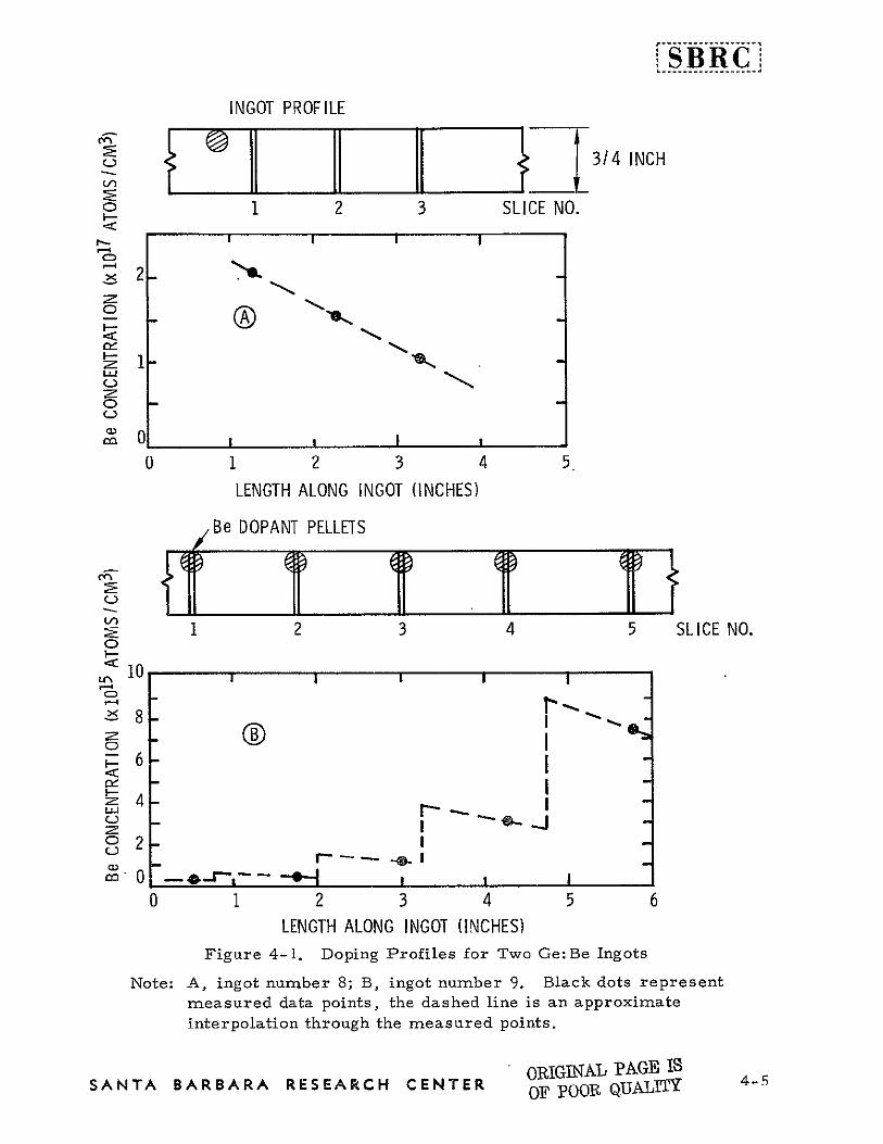
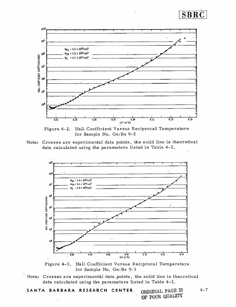

SBRC
ilO 1010
01
N 109[NUe - 13 x 10151cm 3
i L NSA - amp2X 0121cm 3
0D 5 0 0 012 0 14
ill I
Figure 4-4 Hall Coefficient Versus Reciprocal Temperaturefor Sample No GeBe 10-3
Note Crosses are experimental data points the solid line is theoretical
data calculated using the parameters listed in Table 4-2
Table 4-2 Doping Parameters Obtained from Theoretical Fit of Four-Level Model to GeBe Hall Samples
SAMPLE NUMBER PARAMETER UNITS
9-2 03 70-3
0(Be) eV 00204 0102152 0214
e(Be2) eV 0 0568 00699 00643
e(SA) eV 00119 00142 00131 3 x i014N(Be) cm 647 196 x 1015 130 x 1015
-3 x i013 N(SA) cm 523 x i013 514 824 x 1012 N() cm -3 273 x loll 279 ix 250 x Z
C = IONIZATION ENERGY INeV -3N4 DOPING CONCENTRATION INcm
Be1 FIRST BeF ACCEPTOR LEVEL
Be2 = SECOND Be ACCEPTOR LEVEL OIINAL PAGE lBSA -SHALLOW ACCEPTORSR
D = SHALLOW DONORS
4-8SANTA BARBARA RESEARCH CENTER
-shy
The ionization energies obtained for the two Be acceptor levels are
reasonably close to the previously published values of 0 024 and 0 064 eV
The ionization energy obtained for the shallow acceptor is significantly
higher than the accepted literature value of 0 011 eV A similar result was
mentioned previously for the GeGa samples which were tested The reason
for this is not presently known
HALL MOBILITY
The Hall mobility measured on four Ge Be samples is shown in Figure
4-5 as a function of temperature The more lightly doped samples exhibit
a continually rising mobility down to the lowest temperature recorded The
sample with the heaviest doping shows a leveling off at a much lower mobility
This is due to neutral impurity scattering
The low-temperature mobility values of the samples with the lightest
doping (Nos 9-Z and 10-3) are comparable to those measured on the GeGa
samples and are still limited by lattice scattering even though the doping
concentration in the GeBe samples is 3 to 5 times greater This implies
that the neutral Be atom because of a smaller effective size in the Ge
lattice has a smaller scattering cross section
RESISTANCE VERSUS TEMPERATURE
A study of resistance versus temperature behavior was made on three
GeBe samples from crystal 9 and one from crystal 10 The purpose was to
check for hopping conductivity at temperatures below 4 ZK The measureshy
ments were made on surplus GeBe detector chips using the same circuit
arrangement that was used for the GeGa detectors (Figure 3-6) Backshy
ground radiation was excluded from the samples during these measurements
SANTA BARBARA RESEARCH CENTER 4-9
---
SBRCI
i d1 - - I dI _ I I4I
+ --
I1 FRI 1W1
jo I L
E -- -- 1+-
o GeBa 9-2 6 an-l4 II4 65 xTMIx J 0 GeBe 9-4 65 x 10154 0 k I [ ArGiB 9-3 xzGeBe91-3 130X 1015 -L--- i
I I
101 i1100 101 102 103
TEMPERATURE IM)
Figure 4-5 Hall Mobility Versus Temperature for Four GeBe Samples
The results are shown in Figure 4-6 The sample from crystal GeBe 9
with the least Be concentration shows no evidence of impurity hopping conshy
ducitivity As the Be concentration exceeds 1 X 10 15 atomscm 3 we see a
change in slope of the resistance curve at low temperature For the highest
doping concentration of 6 5 X 10 1 5 atomscm 3 a pronounced change in slope
is observed This is clear evidence of impurity hopping conductivity The
effect is to lower the sample resistance by roughly a factor of 50 in the lowshy
temperature range From these data it appears that the Be concentration in
the crystals should be kept below about Z X 10 1 5 atomscm 3 to avoid any
serious lowering of detector resistance due to hopping conductivity
L pAGBORIG OF pOOR QUJALtrt
SANTA BARBARA RESEARCH CENTER 4-10
to
11 G Be -2 t o ~ tot G U I 115
r 0 Irr I ee9 IG 1
R2 022 3z9 h I~ ~ ~ IT X-S1 3 11
Figure 4-6 Resistance Versus Reciprocal Temperature for Four
Uncompensated Ge Be Detectr Samples (QB 0)
The activation energy determined from the slope of the resistance
versus 1T curves is 0 0116 eV corresponding to that of a shallow acceptor
impurity This is to be expected because these Ge Be crystals are not
intentionally compensated with donor impurities Hall eff~ect data presented
in the previous section indicated a shallow acceptor concentration on the
order of 1013 atomscm 3 The hopping conductivity is due to electron
transfer between Be atoms however not between shallow acceptor levels
This obviously must be the case because the Be atom concentration exceeds
the shal low acceptor concentration by a factor of 650
SANTA BARBARA RESEARCH CENTER 4-11
[SB RC
IMPACT IONIZATION BREAKDOWN
Using the same test apparatus shown in Figure 3-6 measurements of
detector resistanc6 (or conductance) were made as a function of bias voltage
(or electric field strength) at two different temperatures The GeBe samples
used were the same four on which the resistance versus temperature measureshy
ments described inthe previous subsection were made Figures 4-7 and
4-8 show the resulting data plotted as conductance versus electric field
strength Figure 4-7 shows data taken at 4 2 0 K and Figure 4-8 shows data
taken at 3 45 0 K (with the exception of sample GeBe 9r4a which was run at
3 00 K)
These curves show a rather complex behavior however they can be
understood in a qualitative way Ohmic conduction occurs only at very low
electric field strengths less than 1 voltcm (This is not immediately
evident with the scale which was chosen for electric field strength but was
observed) As the electric field is increased the sample conductance
increases due to impact ionization of the shallow acceptor levels At 4 20 K
the three samples GeBe 9-2a 10-3a and 9-3a show this in a very proshy
nounced way The other sample GeBe 9-4a does not show this effect so
much because it is dominated by impurity hopping conduction At some
relatively high value of electric field strength impact ionization of the Be
atoms commences and the conductance rises very sharply as indicated by
the upward pointing arrows Sample GeBe 9-Za could not be biased to the
point of impact ionization of the Be atoms because of sample heating which
occurred due to its higher conductance At a 45 0 K a similar behavior is
noted although the shapes of the curves are altered from what they are at
4 2 0 K Also to be noted is the increase in the critical field strength for
impact ionization of the Be atoms when the temperature is lowered from
4 Z0 to 3450K
SANTA BARBARA RESEARCH CENTER 4-1Z
i SBR
-10-]
IV
0 G9e 92a 65bull1014
G Be 9-U 2 0 1015
oC81B9-a 65e 1015 +
lO bull G8 10-3n 1 3 1015
ELETRI FIL STENT N ru3
I
Ge Be Detector Samples at 420 K (QE 0)
n-5
t IAto~l 1
0 Gege 9-4n 67 1014
IOL0 x UeBe9-4e 6 5 1015
10 I
0 v4 0 it I00 IdDELECTRIC STRENGTH GIEMFIELD
Figure 4-8 Conductance Versus Electric Field Strength for GeBe Detector Samples at 345degK (QB 0)
SANTA BARBARA RESEARCH CENTEtR 4-13
Section 5
DETECTOR FABRICATION AND TEST
DETECTOR FABRICATION
Detector chips were cut from the GeGa or GeBe crystals and fabricated
into detector elements using standard processing technology which was
previously developed at SBRC Electrical contacts to the detector were formed
by ion implantation of boron ions This produces a p+-p contact with uniform p+ doping and a highly planar interface with the p-type crystal bulk Each
detector element was assembled onto a tungsten metal mount along with a
load resistor and cryogenic preamplifier This assembly is shown in
Figure 5-1 The load resistor had a nominal value of 5 X 10¹⁰ ohms at 3degK
The MOSFET was a Hughes W164 p-channel enhancement mode device
All GeGa detectors fabricated during this phase of the work were cut
from crystal GeGa 4 However each of the three detectors was made from
a different slice so that an evaluation of the whole ingot would be obtained
Detectors were made from slice numbers Ib 3b and 5b Figure 3-2 showed
the location of these slices in the ingot The Ga doping concentration in the
detectors was Z 5 X 10¹⁴ atomscm 3 All GeBe detectors fabricated were
from the same slice of crystal GeBe 10 The Be concentration in the
detectors was 1 3 X 10¹⁵ atomscm 3
LOW BACKGROUND TEST DEWARS
The detector assemblies were mounted to a two-part cooper heat sink
which was designed to provide a vise-like clamping of the tungsten detector
mount to the copper heat sink This design was chosen to obtain good thermal
conduction to the detector mount A carbon resistor thermometer was imshy
bedded in a hole drilled into the copper heat sink Figure 5-2 shows a
sketch of the heat sink design
SANTA BARBARA RESEARCH CENTER 5-1
J -cmma1c
DRAINTI JA
LOAN
SUBSTRT 0GATEJ
Figure 5-1 Detector - Cryogenic Preamplifier Assembly
ORIGEt PGE
Mounting Detector-Figure 5-2 Sketch of Copper Heat Sink for Preamplifier Assemblies to the Low-Background
SANTA BARBARA RESEARCH CENTER 5-2
LISBRC
This copper heat sink was mounted in a Janis Model RD liquid helium
dewar An aperture defining the sensitive area (-mm X Q- mm) of the
detector was placed directly over the detector and a baffle plate with Z0 mm
diameter aperture was placed directly over that This configuration was
used in an effort to prevent stray radiation from getting to the sides of the
detector A series of aperture plates and cold filters were located between
the detector and the dewar outer window to provide the desired attenuation of
background radiation Figures 5-3 and 5-4 show the filtering arrangements
used in testing GeGa and GeBe detectors Two separate dewars were used
to avoid having to take apart the filtering assemblies and thereby possibly
cause an irreproducible change in the test set up
The background photon flux density arriving at the detector plane was
calculated from the following formula
QB (AX)= Q (300 0 KAX) TRsinZz (5)
where Q(300 0 K AX) = photon irradiance from Zir sterradians of 300K blackbody radiation integrated over the filter pass-band
TR = total peak transmittance of all filters
S = detector field-of-view angle defined by aperture and distance from detector to aperture
The details of this calculation for the different low-background conditions used
in detector evaluation are presented in Appendix A
For GeGa the cold filtering consisted of two special black polyethylene
filters and two neutral density filters The special black polyethylene l 0 acts
as a long-pass filter with a cut-on wavelength of about 80 gim It is a scattershy
ing filter made by mixing various alkali halide crystal powders together with
polyethylene and hot rolling them into a thin film Some carbon particles
also may be in the mixture The true constituents in the film are not known
10 We are grateful to K Shivanandan of NRL for supplying us with this filter material and its relative spectral transmittance curve
SANTA BARBARA RESEARCH CENTER 5-3
SBRC
-_LIQUID NIT(ROGEN LIQU ID-HEL IUM
DETECTOR IPREAMP
BAFFLE PLATE WITHbullram DIAME~TER L -ASSEMBLY
APERTURE AREA DEFINING APERTURE
1mm DIAMETER --- -INSIDE WALLS
FOV APERTURE BLACKENED WITH 3M BLACK VELVET
NEUTRAL DENSITY 7 SPECIAL POLYETHYLENE FILTERS IBOpmCUT-ON)
FILTER
u _ CRYSTAL QUARTZ
BILACKBODY SOURCE (5OOdegK)
CHOPPER MOTOR
Figure 5-3 Low-Temperature Low-Background Dewar Setup for Testing of GeGa Detectors at 100 jim
LIQUID NITROGEN LIQUID HELIUM
DETECTORPREAMP
ASSEMBLYBAFFLE PLATE WITH 2-rm DIAMETER AREA DEFINING APERTURE APERTURE
-mm DIAMETER INS IDEWAL FOV APERTURE BLACKENED WITH
3M BLACK VELVET
NEUTRAL 16- TO 22Nm ORIGINAL PAGE IS DEN4SIT FITR-ooVA FILTER KRS-5 OF POOR
dBLACKBODYSOURCE (SOK)
CHOPPERMOTOR
Figure 5-4 Low-Temperature Low-Background Dewar Setup for Testing of GeBe Detectors
5-4SANTA BARBARA RESEARCH CENTER
SBRC to us The neutral density filters were made at SBRC by evaporating a thinshy
nichrome metal film onto z-cut crystal quartz flats The relative spectral
transmittance of these filters was not measured but was assumed to be
essentially flat in the 60- to IZ0-gLm range The average transmittance of
these filters was checked at room temperature by placing each filter in
front of a dewar containing a GeGa detector (also filtered to detect only
radiation beyond about 60 4m) and measuring the attenuation of the detector
signal from the 500 0 K blackbody source
In most of the GeGa detector testing done on this program a filter
combination was used which gave a calculated background flux QB = I 2 X 10⁹
photonscm 2 sec at the detector plane Measurements on one detector were
made at other background flux levels which were obtained by changing the
neutral density filters and field-of-view (FOV) aperture
For GeBe detector testing a combination of a 16- to 22-gm multilayer
interference band-pass filter I and two neutral density filters was used In
this case the neutral density filters were made by evaporating nichrome
metal onto germanium flats This filtering combination had worked well for
testing doped Si detectors in past work at SBRC and was easy to implement
for the GeBe detectors Admittedly it would be more desirable to test
these detectors in the 30- to 50-4m range however a suitable combination
of filters for this range was not readily available so the 16- to ZZ-gm range
was used instead Extrapolation of NEP data from the 16- to 22-grn range
to 50 jim can be made with little additional expected error The filter comshy
bination used for GeBe detector testing gave a calculated background photon
flux at the detector of QB = 9 X 10⁸ photonscm 2 sec
11 Obtained from Optical Coating Laboratories Inc
SANTA BARBARA RESEARCH CENTER 5-5
-SBRC The signal radiation was obtained from a 500K blackbody located in
close proximity to the dewar outer window A variable speed chopped proshy
vided modulation frequencies from 1 to 1000 Hz The blackbody has a large
opening and the detector looks into this opening through the small FOV
defining aperture located within the dewar Therefore the blackbody radiashy
tion is effectively emanating from this aperture rather than from the blackshy
body cavity itself The blackbody signal irradiance at the detector plane
is given by the formula
HBB (AX) = WBB(AX) ABB TRF (6)Tr DZ
where WBB(AX) = blackbody radiant emittance integrated over filter passband
ABB = FOV defining aperture area
TR = total filter transmittance
F = chopper form factor
D = aperture to detector distance
The signal irradiance on the detector is due to the temperature difference
between the 500 0 K blackbody cavity and the room temperature chopper blade
(assumed to be at 300 0 K) Therefore the signal photon flux density impinging
on the detector is greater than the 300K background photon flux density For
noise measurements the blackbody opening is covered with a shutter so that
the detector then only sees 300K background photons
The blackbody radiant emittance was numerically integrated over the
filter pass-band to obtain that fraction WBB(AX) which would pass through
the filter The details of this calculation are given in Appendix B
The chopper form factor is used to convert peak-to-peak signal
irradiance values to root-mean-square values For the chopper used this
factor had a value of 0 40 A listing of all the parameter values used in
Equations (5) and (6) are given in Table 5-1
SANTA BARBARA RESEARCH CENTER 5-6
Table 5-1 List of Parameters Used in Blackbody Irradiance Calculations
Parameter Units GeGa Ge Be
WBB(AX) wcm Z 3 29 X 10-4 1 53 X 10- Z
-3 - 3ABB cmZ 7 85 x i0 1 96 X 10
TR 181 X 10- 4 1 0 X 10- 4
D cm 8 59 6 65
F 040 040 - IZHBB(AX) w(rms)cm2 8 05 X I0- 13 8 6 x 10
o degrees 067 043
QB(3000 AX) photonssec cmz 149 X 1017 636 x 1017
QB(AX) photonssec cmz 1 Z X i09 0 9 X 10⁹
TEST PROCEDURE
All testing was done in a screen room Tests were performed using a
source follower cryogenic preamplifier and the external circuit components
shown in Figure 5-5 The preamplifier output was coupled to a Quan Tech
Model 206C amplifier which provided a voltage gain of 103 Amplifier
frequency response was flat between IHz and 100 kHz The low-frequency
gain was -3 db at 05 Hz Signal and noise readings were taken on a Quan
Tech Model 304 Wave Analyzer and also visually monitored on an oscilloscope
Tests were designed with the object of evaluating detector performance
as a function of frequency voltage and temperature Data were taken at
0 50 K increments from about 4 50 K down to Z00 K Temperatures below
4 ZK were obtained by pumping over the liquid helium reservoir of the Janis
Dewar A calibrated carbon resistance thermometer mounted in a hole
drilled into the copper heat sink shown in Figure 5-Z was used to monitor
detector temperature
ORIGINAL PAGE IS
SANTA BARBARA RESEARCH CENTER OF POOR QUALITYl 5-7
LsBRCJ S DRAIN
lLOAD ---
RESISTORI I l
QUAN TECHWAVE
IANALYZER
IL I DETECTOR C_ _26~ t MFIER-LOSCILLOSCOPE
SOURCE RES ISTOR
Figure 5-5 Diagram of Circuit Used for GeGa and GeBe Detector Tests
Note Circuit elements within dashed line are at cold temperature those outside are at room temperature
Detector bias was first optimized at the highest operating temperature
which gave a reasonable signal-to-noise (SIN) ratio This was usually
around 4 00 K The temperature was then reduced in 0 5 0 increments At
each new temperature setting signal noise and resistance measurements
were taken at 10 Hz with optimum bias At 3 0degK and 00 K a more detailed
look at detector performance was made At these temperatures the measureshy
ments made were 1) zero bias noise versus frequency Z) signal and noise
versus bias at 10 Hz and 3) signal and noise versus frequency at optimum
bias
RESULTS - GeGa DETECTORS
Three GeGa detectors were fabricated and tested during this program
All were made with material from crystal GeGa 4 Detector 4-lbl-1 showed
optimum SN ratio when operated at a bias voltage of 0 035 volt (0 7 voltcm)
while detectors 4-3b1-i and 4-5bl-I had an optimum bias of 0 0Z4 volt
SANTA BARBARA RESEARCH CENTER 5-8
SBRC
(0 5 voltcm) Detectors 4-lbl-l and 4-361-1 were tested only at one
background flux level namely 1 Z X 10 9 photonsseccm Z Detector 4-5bl-l
was tested at various different background flux levels Figures 5-6 through
5-13 illustrate the relationship between bias voltage resistance signal
noise and NEP of these detectors
The resistance versus temperature data in Figure 5-6 show the same
characteristics as were seen earlier in Figure 3-7 That is detector
4-lbl-l has a lower resistance at any given temperature than either 4-3b1-i
or 4-5bl-i This is due to a lower concentration of compensating donor
impurities in this part of the crystal
Detector 4-5b1-l shows an increase in resistance with decreasing
background flux however the magnitude of this increase is less than expected
Since QB was decreased by a factor of 3 2 detector resistance should have
increased by this factor Instead it only increased by a factor of 1 6 From
this result it might be inferred that the calculated background flux level of
3 7 X 10 8 photonsseccm 2 was in error This could possibly have been the
case However it also should be pointed out that there can be a substantial
error in the resistance measurements reported in Figure 5-6 These are
made by an indirect method through the source follower MOSFET circuit
Appendix B describes this method Also the temperature measurements
could be in error due to the fact that the temperature sensing resistor is not
located on the detector but is some distance away in the copper heat sink
Figure 5-7 shows the detector behavior as a function of bias voltage at
two different temperatures Z 0 and 3 00 K Note that at 3 00 the signal
voltage tends to saturate at higher bias This could be caused by either of
two things 1) the drop in detector ac resistance as bias voltage is increased
or 2) photoconductive gain saturation due to carrier sweep-out Signal
saturation was not observed at 2 00 K operation Similar results were found
on two of the three GeGa detectors tested a tendency toward signal saturashy
tion at 3 0degK but no such tendency at 2 0degK This indicates a much lower
free-hole lifetime at 2 00 K operation
SANTA BARBARA RESEARCH CENTER 5-9
------------
a - p
ol
4-3b-I Q bull 12 x109phsC 2m-2
l4-Tbl-L Q8 - 12x 109 ph sc Cmn2
24-5b1-L Q8 37 x108phsec-I cm 9 1144b11 Oi3 seIDSb-O~-12xI I phsC mm
20 25 30 35 40 45 DETECTOR IMTEMPERATURE
Figure 5-6 Resistance Versus Temperature for GeGa Detectors
SIGNAL 1O-
4 loll
010--5- 10
2 A RESISTANCE -~
E
I~NOISE
10-6-0 9
ORIGINAL PAGE IS
NIPN0 OF POOR QALITY
~2degK 3degK
001 00 a 0 D4o 0w 04060 awo DETECTOR tolts)VOLTAGE
Figure 5-7 Signal Noise NEP and DC Resistance Versus Bias Voltage for GeGa Detector No 4-lbl-l at Two Temperatures (10 Hz Data)
SANTA BARBARA RESEARCH CENTER 5-10
The detector resistance decreases with increased bias This is due
primarily to an increase in free carrier density because of an increasing
lifetime with bias
The noise voltage at low bias is predominantly preamplifier noise As
bias voltage is increased detector noise becomes evident
The NEP is higher at low bias voltage because of the preamplifier
contribution to the noise At higher bias it tends to level off This is
typical of most GeGa detectors that have been tested Some however
have shown a clear minimum and then an increasing NEP at higher bias
probably due to an excess detector noise arising at the detector contacts
The detector signal data in Figures 5-8 and 5-9 can be used to calculate
detector responsivity values and from these one can obtain estimates of
quantum efficiency and photoconductive gain The voltage responsivity at
wavelength X is a function of frequency due to the circuit RC rolloff This
frequency dependence can be written as I
Rv(Xf) = Rv(X o) [1 + (ZlfTRRc)Z] - 2 (7)
where Rv(X o) is the dc or low-frequency responsivity and TRC is the circuit
response time By fitting a curve having the functional dependence on
frequency shown by this equation to the signal data in Figures 5-8 and 5-9
it was found that the 1-Hz responsivity values are sufficiently close to the
dc value to be used in an approximate calculation The 1-Hz voltage responshy
sivity was calculated from experimentally measured data using the formula
RVXI)- S (AX) (8)Rv(X 1) = HBB(AnX)ADg
where S(AX) = signal voltage measured at output of preamplifier
HBB(AX) = blackbody irradiance at detector (see Table 5-1) 3
AD = detector area (7 5 X 10 - cm 2 )
g = preamplifier gain (0 85)
SANTA BARBARA RESEARCH CENTER 5-11
4-lbl- 4-3b1-1 4-5b1-l
10-3
- SIGNAL
04
10-5
-6
NOISE
PREAMPLIFIER
8 l10 - i i i l
1 10 100 1000
FREQUENCY (Hz) Figure 5-8 Signal and Noise Versus Frequency for GeGa
Detectors at 3 00 K
Note Background photon flux density was 1 2 X 10⁹ ph sec - I cm - Z
Signal and noise values are referred to the output of the MOSFET preamplifier
SANTA BARBARA RESEARCH CENTER 5-1Z
SBRCI ----- 1--T-T- -r---------TT--------T-shy
10 _
o 10-5
SIGNAL
0 2
10- 7 PREAMPLIFIER
NOISE
4-1bl-1 QB = 12 x 109 ph sec - I cm -shy 4-3b1-1 QB = 12 x 109 ph se-C mshy2
4-5b1-1 QB = 12 x 109 ph sec - I cm- 2
10_8 4-5b1-1 QB = 37 x 108 ph sec - 1 cm shy 2
1 10 100 1000 FREQUENCY (Hz)
Figure 5-9 Signal and Noise Versus Frequency for GeGa Detectors at Z 00 K
Note Background photon flux density was 1 Z X 10 9 ph sec-I cm-Z Signal and noise values are referred to the output of the MOSFET preamplifier
SANTA BARBARA RESEARCH CENTER 5-13
-SB -RC
The short-circuit current responsivity was calculated from the voltage
responsivity using the equation
is(X 1) = Rv(X 1)R (9)11
where R11 is the parallel resistance formed by the load and the detector ac
resistance values
RacRLH11 = Rac + RL (10)
and
[ V dRdc-Rac = Rdc l - - (11)I Rdc dV
According to detector theory the short-circuit current responsivity is given
by
w e= c GP c (lZ)
Lc = photoconductive gain
7 = free-hole lifetime
S= hole mobility
E = electric field strength
L = interelectrode spacing
77 = quantum efficiency
e = electronic charge
X = wavelength
h = Plancks constant
c = speed of light
Therefore once a value for I(X o) is obtained some estimates of values for
17 and Gpc can be made
Using the foregoing equations and the measured experimental data
values of current responsivity were calculated for the three GeGa detectors
The results for operating temperatures of both 2 0 K and 3 00 K are shown
in Table 5-Z The current responsivity values are at the peak of the detectors
SANTA BARBARA RESEARCH CENTER 5-14
i-SBRCj]
Table 5-Z Parameters Used in Calculation of Short-Circuit
Current Responsivity for GeGa Detectors
DETECTOR NUMBER TEMPERATURE PARAMETER UNITS 4 (OK)
4-]b1-1 4-3b1-1 4-5b1-1
BIAS VOLTAGE VOLTS 0035 0024 0024 20 AND 30 ELECTRIC FIELD VOLTSICM 070 048 048 20 AND 30
10 x I010 Rdc OHMS 5 K 109 14 x 10I0 30
Rac OHMS 28x 109 73 x 109 Li x 1010 30
S(AX 1) MILLIVOLTS 044 020 019 30
RV(Ap 1) VOLTSIWATT 86 x i010 39 X 1010 37 x 1010 30
Is(p 1) AMPS WATT 32 (10) 61 41 30
nGpc (0124) 0076 0051 30
Rdc OHMS 16 x 1010 20 x 1010 31 x 1010 20
Rac OHMS 12 x 1010 13 X 1010 24 x 1010 20
S(441) MILLIVOLTS 023 012 015 20
x 1010 Rv(Xpl) VOLTSWATr 4 5 X 10¹⁰ 23 29 x 1010 20
Is(Ap 1) AMPSWAnT 46 22 18 20
flGpc 0057 0021 0022 20
RL - 5 x 10¹⁰ (NOMINAL VALUE)
Xp = 100 Pm 0hAT VAGE IS
AD - 7 5 x 10⁻³ cm2 (15 x 05 mm) ORUGNL- ALI OF pOOR Q
f =IHz
pm An exceptionallyspectral response curve which was taken to be 100
0 high value of current responsivity was obtained for detector 4-lbl-l at 3 O K
No obvious experimental error could be found in the data however the result
does seem to be spurious By comparison of the Z 00 and 3 00 K current
value around 10responsivities of the other two detectors it appears that a
ampswatt would be more appropriate for this detector The current
responsivity for this detector would be expected to be somewhat higher than
the others because of a higher applied bias and longer free carrier lifetime
Both ofthese conditions lead to a higher photoconductive gain for this detector
The signal versus bias voltage data shown previously in Figure 5-7 indicate
that the photoconductive gain could be on the order of 0 5 (This result is
of course based on the assumption that the maximum value of the gain at
saturation is 0 5 ) The use of these results in Equation (12) leads to a
5-15SANTA -BARBARA RESEARCH CENTER
quantum efficiency of 0 Z5 which seems reasonable considering the Ga doping
concentration used in these detectors The other two detectors probably are
operating with a photoconductive gain around 0 Z at 3 O0 K For Z 00 K
operation a decrease in current responsivity by a factor about 2 5 is
observed This must be attributed to a decreased photoconductive gain of
the same amount since the quantum efficiency would not be expected to
change simply because of a change in operating temperature
The measured signal-and-noise data was used to calculate the NEP
data which is shown in Figures 5-10 5-11 and 5-1Z The NEP versus
frequency data shows an essentially flat behavior from 1 to 40 Hz and then
rises slowly An effort was made to measure detector noise data at frequencies
below 1 Hz using a spectrum analyzer The data obtained were unreliable
thus not reported here
The NE versus temperature data of Figure 5-12 show a fairly clear
minimum at 3 00 K operation At higher temperatures NEP increases due to
increasing detector generation-recombination noise and decreasing detector
resistance At lower temperatures the NEPincrease is mainly due to a
decreased detector responsivity The conclusion is that the optimum operatshy
ing temperature is close to 3 00OK NEP values of about 0 7 to 1 X 10-16 1
wattsHz2 were achieved with a background flux of 1 2 X 10⁹ photonsseccm Z
One detector number GeGa 4-5b-i was also measured at various
different background flux levels Figure 5-13 shows a plot of calculated NEP
values versus frequency at four different flux levels At the highest backshy
ground flux NEP rises in the low-frequency range This is due to 1f noise
in the detector At the lower background flux levels NEP shows less
dependence on frequency and is reasonably flat down to 1 Hz - The lowest1
-measured NEP was 4 X 10 - 1 7 wattsHz at I -lz with a background level of
3 7 x 10 8 photonsseccm z
SANTA BARBARA RESEARCH CENTER 5-16
10-15 iI iF ---- I~t T--
T4-lbl-1 QB 12 x 109-E s---f1j2 -I -2
4-3b1-1 QB = 12 x 109 ph sec cm 1 -2
4-5b1-1 QB = L2 x 109 ph sec- cm
QB -37 x 108 ph sec- cm -2 4-5b1-I
1 1 4 - - --- o
1 0 -17 [ 1 1 1 1 1 I1 1 1 II I
1I0 100 1000
FREQUENCY (Hz)
Figure 5-10 NEF Versus Frequency for GeGa Detectors at 3 OdegK
10-1
I -2 4-Ibi-1 QB - 12 x 109 ph sec cm
I -2 4-3bl-1 QB = 12 x 109 ph sec cm
I 24-5bl-1 Q8 12 x 109 ph sec Cm
- 2 4-56l1-I 37 x 108 phsec 1 cmQB shy
__ 1
iiiI fl LLII I it
1 10 100 1000
FREQUENCY (Hz)
Figure 5-11 NEP Versus Frequency for GeGa Detectors at Z00 K
SANTA BARBARA RESEARCH CENTER 5-17
iSBRC]
4-1E- OB 1]2 x ]09 ph sle c 2
4-31-L Q8 L2 X109ph se-t cm-2 4-b1-1 QB - 12 x 109 phse 1 cm 2
4-5b1-L QBshy3 7 X10⁸ ph seC1 cm -2
t
I IT
-----I
1WI71
20 25 30 3r5 4 0 4 5
TEMPERATURE(K1
Figure 5-1Z NEP Versus Temperature for GeGa Detectors at a Frequency of 10 Hz
SQB- 124 x 109 phseccm2
QR 3 7 x 10⁸ phlseclcm2
Q8 = 175 x 1010 phlseccm 2
BQ 117 x j112 phseclcm2
10_14 _________ ________ _______
- NOTE SCALE CHANGE
S --shy _-shy
1 10 100 1000
FREQUENCY (Hz)
Figure 5-13 NEP Versus Frequency for GeGa Detector 4-5b-I at 3 00 K for Four Different
Background Flux Levels
SANTA BARBARA RESEARCH CENTER 5-18
r ---------------SBRC
RESULTS - GeBe DETECTORS
As mentioned previously all three GeBe detectors fabricated and
tested on this program were cut from the same slice of crystal Ge Be 10
The slice number was 3a and the location of this slice in the crystal was
adjacent to slice 3 from which the Hall sample was taken The Be doping
1 3 X 10 1 5 concentration was atomscm 3 Figures 5-14 through 5-Z0
illustrate the relationship between bias voltage resistance signal noise
and NEP of these detectors lt
In Figure 5-14 the signal is seen to be a linear function of bias voltage
and does not tend to saturate as did the GeGa detectors The resistance is
seen to be nearly constant with bias voltage to it can be assumed that Rac
is equal to Rdc The NEP is higher at low bias due to preamplifier noise
and then decreases tending to flatten out as bias increases This is quite
evident at Z 00 K operation but for this particular detector at 3 00 K the
NEP starts rising prematurely due to excess detector noise The other
detectors tested showed the flatter NEP curve at both operating temperatures
Figure 5-15 shows the measured resistance versus temperature data
The detectors all have similar resistance values as would be expected for
detectors cut from the same slice of material Since this material did not
show significant hopping conductivity the resistance is background photon
limited at the lowest temperatures with a value of Z 5 X 10 1 0 ohms This
resistance value is substantially lower than might be expected based on a
theoretical calculation The background limited dc resistance can be
expressed as
Rdc - L cflQBTepiw
(13)
ORIGINAL PAGE IS OF POOR QUALITY
SANTA BARBARA RESEARCH CENTER 5-19
--- S- --- -shy
- ~ SIGIAL
---20K
i0 5 IOU
6I0- -1-
NOISE RESISTANCE
Detector Voltage for CeBe l0-3a-3 at TwoTemperatues 2degK and 3K
-10-33-1 10-3a-2
010-ashy
109
20 2 303540 45s DETECTOR (KT5MPERATURE
Figure 5-15 Resistance Versus Detector Temperature of Ge Be Detectors
Note Background photon flux density was 0 9 X 10 9 ph sec-1 cm-2
SANTA BARBARA RESEARCH CENTER 5-Z0
LSBRC
Inserting the following values into this equation
- ZL = 5 X 10 cm
T7 =03
QB = 9 X 10⁸ photonsseccm Z
i =10 - 7 sec
e = 16 Xl0- 1 9 coul
ii = 4 X 10⁵ crZvolt sec
w = 1 5 y0-1 cm
gives a value for Rdc of 1 9 X i01 ohms nearly an order of magnitude
higher than measured All the above parameters except 71 QB and T came
from direct measurements The 77and T values are reasonable approximations
which should be within a factor of 2 or 3 of the true values It would be
necessary to increase the 77 product by a factor of 10 to bring the calculated
Rdc into agreement with the measured value This seems to be unreasonable
therefore it must be concluded that QB is actually higher than the stated
value of 9 X 10⁸ photonsseccm z
Figures 5-16 and 5-17 show measured signal-and-noise data versus
frequency for two operating temperatures The signal data can be analyzed
in the same way as for the GeGa detectors to obtain short-circuit current
responsivity values and estimates of the 1]Gpc product The results are given
in Table 5-3 The blackbody signal radiation was restricted to the 16- to
22-gim band by a filter Therefore direct use of Equation (8) gives the
voltage responsivity at a wavelength of -about 19 pLm To convert this value
to responsivity at the peak of the GeBe spectral response which is at 40 pLm
the calculated responsivity was multiplied by a factor of 2 This factor is
based on the relative spectral response of GeBe reported by Shenker et al 12
All the values of voltage and current responsivity listed in Table 5-3 are at
the detectors peak wavelength of 40 pLm The calculated current responsivity
values are seen to be in the neighborhood of 2-5 ampwatt DetectorGeBe 10-3a-3
1Z See Reference 5
SANTA BARBARA RESEARCH CENTER 5-21
tllm I - r rt irn I ITII41
10-3a-1 10-3a-2 10-3a-3
10-3 N
SIGNAL
10shy4
J4______
-
C
10-5
CNOISE
PREAMPLIFIER NOISE 10-7 shy
-RIGINAL PAGE IS OF POOR QUALTY
1 10 100 1000 FREQUENCY (Hz)
Figure 5-16 Signal and Noise Versus Frequency for GeBe Detectors at 3 00 K
Note Background photon flux density was 0 9 X 1-09 ph sec- 1 cm-Z Signal and noise values are referred to the output of -the MOSFET preamplifier
5-ZZSANTA BARBARA RESEARCH CENTER
l II IIIII~~~SR
-L1B3ashy
10-3a-1 - ------10-3a-2 --- 10-3a-3
10- 41______ __
10-4
a V SIGNAL
-shy4
PREAMPLIF IERNOS
- 810 1 a I l i l t I J l
1I0 100 1000
FREQUENCY (Hz)
Figure 5-17 Signal and Noise Versus Frequency for GeBe Detectors at 2 OdegK
Note Background photon flux density was 0 9 X 10 9 ph sec-i crn-Z
Signal and noise values are referred to the output of the
MOSFET preamplifier
SANTA BARBARA RESEARCH CENTER 5-23
SBRC L -
Table 5-3 Parameters Used-in Calculation of Short-Circuit Current Responsivity for GeBe Detectors
UN ITS DETECTOR NUMBER TEMPERATUREPARAMETER 10-3a-3 (OK)10-3a-1 1O-3n-2
BIAS VOLTAGE VOLTS 0235 0235 0082 30 ELECTRIC FIELD VOLTSICM 470 470 164 30
Rac OHMS 19 x 1010 22 x 1010 18 x 1010 30 S(AX 1) MILLIVOLTS 18 19 056 30
Rv(Xp 1) VOLTS(WAT 66 x 1010 69 x 1010 20 x 1010 30
Is(Xp 1) AMPSWAIT 57 54 18 30
flGpc 0176 0167 0056 30
BIAS VOLTAGE VOLTS 0259 0353 0188 20
ELECTRIC FIELD VOLTSICM 519 705 376 20
Rac OHMS 22 x 1010 26 x 1010 27 x 1010 20
S(AX 1) MILLIVOLTS 15 11 11 20
Rv(Ar 1) VOLTSIWAIT 55 x 1010 40 x1010 40 x 1010 20
Is(Xp 1) AMPSIWATT 43 29 28 20
1GPC 0133 0090 0081 20
RL =3 x 10¹⁰ OHMS (NOMINAL VALUE)
Ap = 40 pm AD 75 x 10-3 cm2 15 x 05 mm)
I =1 Hz
was somewhat lower than the other two because it had to be operated at a
lower bias voltage If one assumes a quantum efficiency of 0 3 then the
photoconductive gains would be in the range of 0 2 to 0 6 These are
reasonably values for the low-frequency gain (I Hz) which would not be
limited by carrier sweep-out
Calculated NEP values are plotted versus frequency and temperature
in Figures 5-18 5-19 and 5-20 Figures 5-18 and 5-19 show the NEP to be
essentially flat with frequency between I and 10 Hz and then rising for higher
frequencies An exception is Detector GeBe 10-3a-Z which appears to have
some excess noise in the I- to 2-Hz range causing an increased NEP at these
low frequencies
5-24SANTA BARBARA RESEARCH CENTER
ISBRCI
-10-14
10-3a-I 10-3a-2 -
S 10-3a-3shy
-15 10 shy
IO-16 l
1 10 100 1000 FREQUENCY (Hz)
Figure 5-1-8 NEP Versus Frequency for GeBe Detectors at 3 00 K
- I - Z Note Background photon flux density was 9 X 10⁸ ph sec cm
10-14 j1n --- 1 i-- r- r r rr
1O-3a-1 110-3a-2
- -- 10-3a-3
0-1
1o-16 ORIGINAL PAGE IS OF POOR QUALITY
- 1 7 10 1 1 1 1 I Ii t - 1 -1 1 t 1I I l
1 10 100 100
FREQUENCY (Hz)
Figure 5-19 NEP Versus Frequency for GeBe Detectors at 2 00 K
- -z Note Background photon flux density was 9 X 10⁸ ph sec I cm
SANTA BARBARA RESEARCH CENTER 5-Z5
SBRCI
The NEP versus temperature data in Figure 5-Z0 showa reasonably
flat behavior between Z 0 and 3 00 K and then rise at higher temperature
An exception here is detector GeBe l0-3a-3 which reaches its lowest NEP
only at Z 00 K This ditector had to be operated at a lower bias voltage than
the others because it became excessively noisey at higher bias This
problem was most likely due to contact noise The minimum NEP is about
the same for all three detectors and is Z to 3 X10⁻¹ 6 wattsHz2
10-3a-I 10-3a-2 10-3a-3
15 10shy
=
-10 16 1 I 1 3 1 I 20 25 30 35 40 45
DETECTOR TEMPERATURE (OK)
Figure5-ZO NEP Versus Detector Temperature for GeBe Detectors
Note Background photon flux density was 9 X 10 8 ph sec-1 cm-Z
SANTA BARBARA RESEARCH CENTER 5-26
Section 6
CONCLUSIONS AND RECOMMENDATIONS FOR FUTURE WORK
This work has provided significant advancements in the technology of
GeGa and GeBe photoconductive detectors for use in astronomical observashy
tions at wavelengths from 30- to 1Z0-gm All the major goals for this phase
of the development were accomplished The primary conclusions that can
be drawn from the work performed thus far are as follows
GeGa DETECTORS
A Ge purification method was developed which reduces the residual
donor impurity concentration to the 1010 atomscm 3 range Residual
acceptor impurity content may be much higher but is inconsequential
to detector performance
shown to produce Introduction of Ga by the zone leveling method was
uniformly doped ingot with sufficient material for fabrication ofa many detectors The doping concentration can be controlled within
an acceptable tolerance
Crystals doped to Z 5 X 10¹⁴ Ga atomscm 3 do not show hopping
conductivity Higher doping concentrations might be useful for
increasing the detectors quantum efficiency
Short-circuit current responsivity for 100 gm radiation was measured
to be in the range of 6 to 10 ampswatt at 3 0 0 K operation This
implies an 77Gpc product of 0 074 - 0 IZ4 Quantum efficiency was
estimated to be around 0 25
Detectors were not enclosed in an integrating cavity The use of
such a scheme 1could significantly improve quantum efficiency
An NEP of 4 X 10-17 wattsHz2 was measured at 1 Hz with a backshy
ground flux of 3 7 X 10⁸ photonsseccm Z at 3 00K operating
temperature This comparesfavorably with the calculated BLIP
value of 1 X10-17 wattsHz2 (77 =-0 30 Xp = 100 gm)
The NEP is minimized at an operating temperature very close to
3 0degK Higher or lower operating ter-peratures may cause a
degradation of NEP
Reproducibility and yield of good detector elements were excellent for
GeGa detectors Most of the technology development on this material
has been completed and the producibility of detectors which meet or
exceed the NEP objectives for the IRAS mission has been demonstrated
SANTA BARBARA RESEARCH CENTER 6-1
SBRC
GeBe DETECTORS
Oxygen must be eliminated during growth of GeBe crystals to prevent Be-O complexing A vacuum zone melting process was developed which provided a method for doing this
10 1 5 The Be concentration should be kept below Z X atomscm 3 to prevent impurity hopping conductivity from seriously lowering detector resistance at 3 00 K
The electric field strength that can be applied to uncompensated GeBe is limited to less than 10vcm due to impact ionization of shallow acceptor levels
o Short-circuit current responsivity for 40 pLm radiation was measured
to be in the range of Z to 5 ampswatt for 3 00 K operation
Detectors were not enclosed in an integrating cavity The use of such a scheme could significantly improve quantum efficiency
- 1 6 O The lowest measured NEP for GeBe detectors was 2 to 3 X 10
wattsHz I
at a frequency of I Hz with a background flux of 9 X 10⁸
photonsseccm 2 The BLIP value for this background is 4 6 x( i017 wattsHzi (7 = 0 3 Xp = 40 ptm)
The NEP is optimized at 3 00 K or lower There was no clear indication of a minimum in the NEP versus temperature plot
The yield of GeBe detectors from a given slice of material was acceptable Two out of three detectors fabricated and tested had reasonably good performance the third had excessive 1f noise
The uniformity of GeBe material properties within a slice is excellent Uniformity over a whole ingot has not yet been achieved
The producibility of GeBe detector elements is presently limited by the crystal material uniformity and quality
RECOMMENDATIONS FOR FUTURE WORK
In the case of GeGa recommendations for future work could be called
minor technological improvements The work accomplished to date has
shown that GeGa detectors can meet the objectives of the IRAS mission
However minor improvements might still be achieved For example
GeGa crystals with a Ga concentration greater than Z 5 X 10¹⁴ atomscm 3
should be grown and evaluated to see if the quantum efficiency can be
improved Also the use of integrating cavities for improvement of quantum
efficiency should be investigated
SANTA BARBARA RESEARCH CENTER 6-2
Measurements of detector behavior at frequencies below I Hz should
be made Although data taken to date show no evidence of any problem in
this frequency range confirming measurements should be made
In the case of GeBe the crystal growth technology needs further
improvement It is recommended that more work be done in two areas
First the method of zone leveling to produce a uniform Be concentration
along the whole ingot should be implemented With the existing method
variation of Be concentration along an ingot is still too great to give a
sufficient quantity of material for focal plane array production Secondly
crystals of compensated material should be grown and evaluated to see if they
have any advantage over the uncompensated material which has been used
in past work The uncompensated material must be operated at low electric
field strengths to prevent impact ionization of the shallow acceptors In
compensated material electric field strengths 4 to 5 times larger should
be permissible This could give an improvement in photoconductive gain
provided that the hole lifetime is not seriously degraded by the additional
compensating donors Careful control will be needed to avoid introduction
of too manV compensating donors
As mentioned for the case of GeGa detectors the use of integrating
cavities should also be investigated for GeBe detectors Finally measureshy
ments of detector behavior at frequencies below I Hz should also be made
SANTA BARBARA RESEARCH CENTER 6-3
-SBRC-
Appendix A
IRRADIANCE CALCULATIONS
This appendixpresents details of the calculation of blackbody signal
irradiance and background photon flux density at the detector focal plane in
the low-background test dewars
GeGa TEST DEWAR
As mentioned in Section 5 in the main text the GeGa detectors were
tested using a long-wavelength pass filter consisting of two pieces of special
black polyethylene and crystal quartz These materials along with the
detectors natural cutoff at about 120 pLm produced a relative spectral response
as shown in Figure A-1 This isolated a spectral band about 35 pLm wide
in the 100-pim region Neutral density filters were also used to further
attenuate the background photon flux on the detector
The effective blackbody signal irradiance on the detector was calculated
by numerically integrating the blackbody flux over the filter spectral range
To do this the spectral range was broken up into intervals each 5 pLm wide
as shown in Figure A-1 The blackbody radiant emittance for each spectral
interval was then obtained from a radiation slide rule These values are
shown in Table A-1 along with the spectral intervals and the relative filter
transmittance in each spectral interval Since the signal radiation is
produced by the difference between the 500K blackbody and a 300 0 K chopper
blade these values were obtained from the slide rule and one was subtracted
from the other to obtain the actual signal radiant emittance in each interval
The difference values are listed in column 5 of the table Multiplication of
each number in column 5 by the corresponding -relative filter transmittance
SBRC is indebted to K Shivanandan of NRL for furnishing these data
SANTA BARBARA RESEARCH CENTER A-1
10
09
r
I
-n
L
08 r
07
L
06 I
Co
c4 05
LO
II I 04
03 I
r
-IL
I
I
II
02 SI I
01
I
0 50
I
60
Figure A-I
I
70 80 90 100 110 120 WAVELENGTH (pm)
Relative Spectral Response of GeGa Detector with Long Wavelength Pass Filter
I
i
130
SANTA BARBARA RESEARCH CENTER A-Z
V) Table A-i Listing by Spectral Interval of Blackbody Signal Radiant Emittance and gt Background Photon Flux Values Used for GeGa Detector Testing z -i
(1) (2) (3) (4) (5) (6) (7) (8) w (X)gt RF(X) W500(A) W300(X) W500(X) -W300(X) WBB(A) Q30O QB(X)
4m) (wcm2) (wlcm2) (wcm2) (wcm2) (phseccm2) (phseccm2)
x1O3 x1O-3 xlO- 3 xO-5 xl017 x 016
S40-45 0 1436 0670 0766 0 1430 P
m 45-50 0 0912 0444 0468 0 1060 0
r 50-55 0 070 0 632 0310 0322 2254 0818 057
gt 55-60 0125 0454 0230 0224 2800 0664 083
60-65 0165 0334 -0172 0162 2673 0540 089
65-70 0260 0248 0130 0118 3068 0441 115
m 70-75 0320 0190 0100 0090 2880 0364 117 z 75-80 0375 0150 0080 0070 2625 0312 117
0257 150 m
80-85 0585 0118 0062 0056 3276
85-90 0685 0094 0050 0044 3014 0220 151
90-95 0810 0076 0040 0036 2916 0186 151
00 95-100 0950 0058 0032 0026 2470 0157 149
00 100-105 0900 0050 0028 0022 1980 0144 130
0105-110 0750 0040 0020 0020 1500 0108 081
0102 061110-115 0600 0032 0018 0014 0840
115-120 0350 oo 0016 ~ WB(X 3o_910-4ooo 0030 ~ oooo0014 0490 0094 033
120-125 0100 0027 0014 0013 0130 0086 009 ~~~
QB( 300AX) =149 x 1017SUMMATION WBA)=32x0
ISBRC
in column Z gives the effective blackbody radiant emittance in each spectral
interval These values are listed in column 6 Summation overall spectral
intervals then gives the total blackbody radiant emittance in the filter pass band
This total radiant emittance number is then used in Equation (6) to
calculate the irradiance at the detector focal plane Also needed for this
calculation are the absolute peak transmittance values for each filter and
the dewar window These are as follows
Absolute Peak Transmittance
1 Quartz window 0 85 First neutral density filter 0 015 Second neutral density filter 0 06 Z Special black polyethylene filters (0 5Z) Z
Atmospheric water vapor 0 88
Total transmittance TR = 1 8 X 10- 4
A transmittance factor for atmospheric water vapor was also included
Although this produces a small effect on total transmittance it was found to
be not negligible The effect of atmospheric absorption was checked by
flushing the space between the blackbody opening and the dewar window with
dry nitrogen This produced an increase in a GeGa detectors signal by 13
Since it was impractical to continue flushing this space during all tests
the atmospheric correction factor was applied to the blackbody irradiance
calculation
The equation for signal irradiance Equation (6) in Section 5 was
written as WB(ZX)AB TR F
HBB(AX) = WBB(AX) BB (AI) SN DZ
A-4SANTA BARBARA RESEARCH CENTER
Substituting the values calculated above along with those other values listed
in Table 5-I gives
HBB(AX) _ (3 29 x 10-4)(7 85 X 10-3)(1 8 x 10⁻⁴)(0 4) - o xI - 13 wcm 2 (3 14) (8 59) Z
The background photon flux density at the detector plane was calculated
in a similar manner Column 7 of Table A-I lists 300 0 K photon flux density
values for each spectral interval as obtained from a radiation slide rule
Column 8 gives the effective values passing through the filter (column Z X 7)
and their sum over all the spectral intervals
Equation (5) in Section 5 was then used to calculate the background
photon flux density at the detector plane This equation is
QB(AX) = Q(300 0 K AX) TR sinz 82 (AZ)
The filter transmittance factor in this case does not include the outer
warm quartz window nor does it include the atmospheric water vapor loss
It includes just the two neutral density filters and the two special polyethylene
filters Thus TR = 2 4 X 10- 4 Using this value along with the appropriate
values from Tables A-I and 5-1 gives
BX) = (149 X 1017)(Z 4 X 10-48 59) = 1 Z X 109 phseccm z
CeBe TEST DEWAR
The GeBe Detectors were tested using a 16- to 2Z-vrn multilayer bandshy
pass filter plus neutral density filters on germanium The relative transshy
mittance curve for this band-pass filter is shown in Figure A-2 The blackshy
body signal irradiance through this filter was calculated by numerical
integration in the same manner as was described for the case of GeGa
Table A-Z lists the relevant data
sectRGIN AL
SANTA BARBARA RESEARCH CENTER A-5
09
08 I I I
II I IL I I I I
06-C
04 I I
03shy
02
01 I
15 16 17 18 19 20 21 22 23 24
WAVELENGTH (um)
Figure A-Z Relative Spectral Response with Band-Pass Filter
of GeBe Detector
A-6SANTA BARBARA RESEARCH CENTER OO 0 A-6uA yOF P00R
z -I wgt
gt
X
Table A-Z Listing by Spectral Interval of Blackbody Signal Radiant Emittance Background Photon Flux Values Used for GeBe Detector Testing
and
gt
m
(1)
X 10m)
(2)
RF(X)
(3)
W5go(X) (wlcm2)
(4)
W30j(X) (wlcm2 )
(5)
W500) - W30 ijX) (wcm2)
(6)
WBB(A) (wlcm2)
(7)
Q3 0(X) (phlseccm2)
(8)
QB(X) (phseccm2)
m gtx
0 -
m Z -1 m1
15-16 16-17
17-18 18-19
19-20
20-21
21-22
22-23
23-24
005 080
078 091
086
072
045
037
015
770 630
525 455
385
350
280
245
210
x I0-
220
175
152 138
129
110
097
087
074
x Io-3
550
455
373 317
256
240
183
158
136
x io-3
028
364
291 289
220
173
082
058
020
x i017
156
144
140 131
123
115
1-03
098
090
xI017
008
115
109 119
106
083
046
036
014
SUMMATION WBB(AX) 153 x 10-2 QB3 0QAX) 63 1017
0
4 lo
-SB-R--
Using the data from Tables A-Z and 5-I and substituting into Equation
(A l) gives
HBB(UX) = (1 53 X 1 0 -Z)(1 96 X 10-3)(1 0 X i0-4)(0 4) = 8 6 X 10 - I Z wcm Z (3 14) (6 65) Z
The background photon flux density at the detector was obtained by subshy
stituting data from Tables A-1 and 5-1 into Equation (AZ) to get
QB(300K A) = (6 36 x 1017)(1 0 X 10 -6 65) = 9 0 X 108 phseccm Z
DETECTOR RESPONSIVITY
The blackbody signal irradiance values calculated in this appendix were
used to obtain detector responsivity by the usual formula
V9(AX) (M) Rv(A) - HBB(AX) AD
where Rv(X) is the responsivity in voltswatt VS(AX) is the measured signal
voltage AD is the detector sensitive area and HBB(AX) is the effective signal
irradiance It turns out that this procedure yields the responsivity at the
peak of the filter spectral distribution Xp A derivation of this result is as
follows
If Rv(X) is the detector responsivity at any wavelength and Pgt is the
signal power per unit of wavelength (wattsnLm) on the detector at this waveshy
length then for a given wavelength range between X and XZ the detector
signal voltage will be given by Xz
Vs(AX) = f Rv(X) PX dX (A4) X 1
where AX refers to the spectral interval X1 - XZ
SANTA BARBARA RESEARCH CENTER A-8
L[SBRCJ
If the detectors Rv(X) curve is expressed as a relative response
normalized to unity as shown in Figures A-I and A-Z then equation (A4)
can be written as Xz
VS(AX) = Rv(Xp) f RR(X) PX dX (A5)
where RR(X) is the relative response ( 1 at Xp) and Rv(Xp) is the responsivity
at X p This equation can be rewritten as
Rv(Xp) = XV (A6)
j RR(X) PX d xl
The integral in the denominator is the same as HBB(AX) AD when
HBB(AX) is calculated by the numerical integration method described
previously in this Appendix Therefore the responsivity calculated from
equation (A3) is the responsivity at the peak of the relative spectral response
curve Xp
SANTA BARBARA RESEARCH CENTER A-9
Appendix B
DETECTOR RESISTANCE MEASUREMENTS THROUGH MOSFET
This appendix describes the method used for determining detector
resistance values when the detector is connected to the cryogenic MOSFET
source follower preamplifier
The circuit diagram is shown in Figure B- i The detector dc resistance
is given by
Rdc = VDI (B1)
where
I = VB(RL + Rdc) (BZ)
The voltage drop across the detector VD will appear at the MOSFET source
terminal multiplied by the gain of the source follower This voltage is
measured by observing the change in V S as the detector bias voltage is
switched from zero to ON Thus
V D = AVs0 85 (B3)
where LV S is the observed charge in source voltage and 0 85 is the source
follower gain Combining equations (BI) (BZ) and (B3) gives
Rdc RL ((B4)(085 yv) -1
Use of this equation requires prior knowledge of the load resistance
RL Since the load resistance value can vary with temperature and bias
voltage this may introduce considerable error into the determination of
Rdc by this method Values of VB and AVs can be measured with good
precision and will not produce a large error
SANTA BARBARA RESEARCH CENTER B-I
- ------------
VB I
LOAD I RESISTOR RL
DVs
DETECTOR I- Rdc I
L----- --
VB = BIAS VOLTAGE APPLIED EXTERNALLY ACROSS BOTH DETECTOR AND LOAD
= VOLTAGE DROP ACROSS DETECTORVD
VS = SOURCE VOLTAGE
Figure B-I Circuit Diagram for Low-Background Detector Testing
Table B-i shows measured resistance values versus temperature and
applied voltage for a typical load resistor used in the detector assemblies
delivered on this program It is clear from these data that good calibration
of the load resistor must be accomplished to obtain accurate values for
Rdc from equation (B4)
Table B-I Resistance Versus Temperature of Typical Load
Resistor Used in IRAS Device Assemblies
Resistance (Q) Resistance (Q) Resistance ()Temperature at at at
(K) OZO V 0zoo V Z00 V
I0 1 04 Z 3 8 X 10¹⁰ 3 7 x Z 7 X 10¹⁰
4 0 3 7 X 10¹⁰ 3 9 X 10¹⁰ 28 X 101 0
0 4 7 X 10 1 0 1 03 5 44 X10 1 3 2 X10
03 0 5 1 x I0 6 0 x I010 3 7 X 10 1 0
ORIGINAL PAGE 18 B-Z
SANTA BARBARA RESEARCH CENTER OF POOR QUALITY
Another obvious method for determining Rdc would be to attach an
additional wire to the detector at the connection to the MOSFET gate and
bring this lead out of the dewar Measurements of detector current and
voltage could then be made directly However tw6 problems arise with
this method First the additional lead to the detector produces an added
capacitance at the gate input which will cause the circuit response to roll
off at lower frequencies Since the combination of MOSFET gate input andshy
detector capacitance is only about 5 pf distributed capacitance from the
additional wire bould easily equal or exceed this value Secondly the
insulation resistance of the dewar feed-throughs has to be very high in fact
much higher than the detector resistance If detector resistance values are
in the 10 1 0 -ohm range the insulator resistance should be greater than i0 1 Z
ohms The metal-glass feed-throughs used on our dewars can have this
high an insulation resistance if properly cleaned and kept dry However
past experience has shown that they are easily contaminated with use and
leakage problems result It was because of these problems that the indirect
method of detector resistance measurement described above was adopted
SANTA BARBARA RESEARCH CENTER B-3
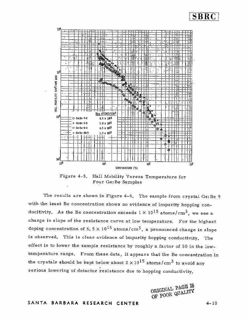
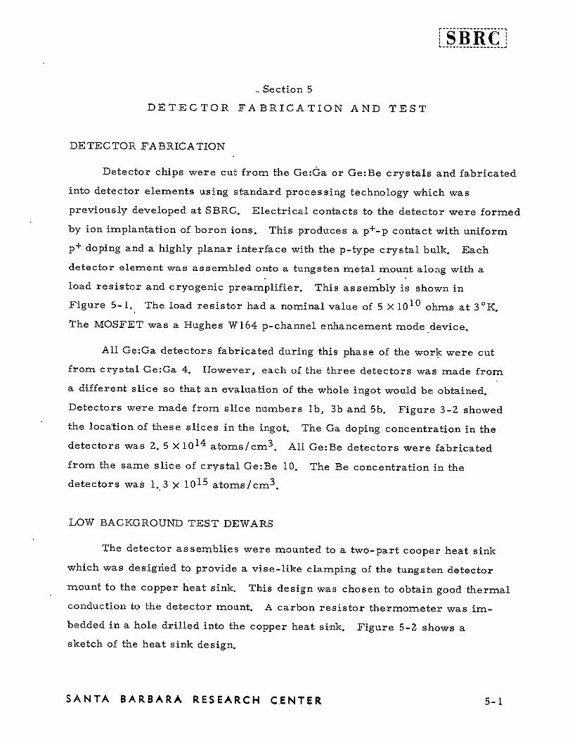
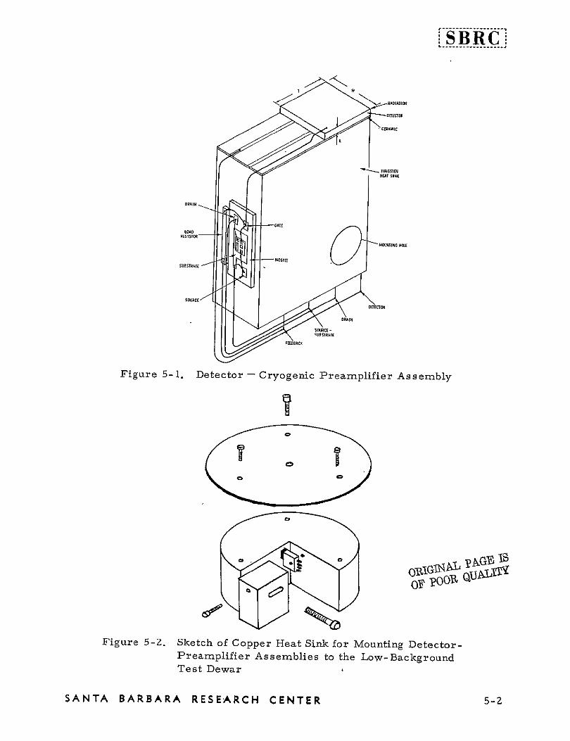
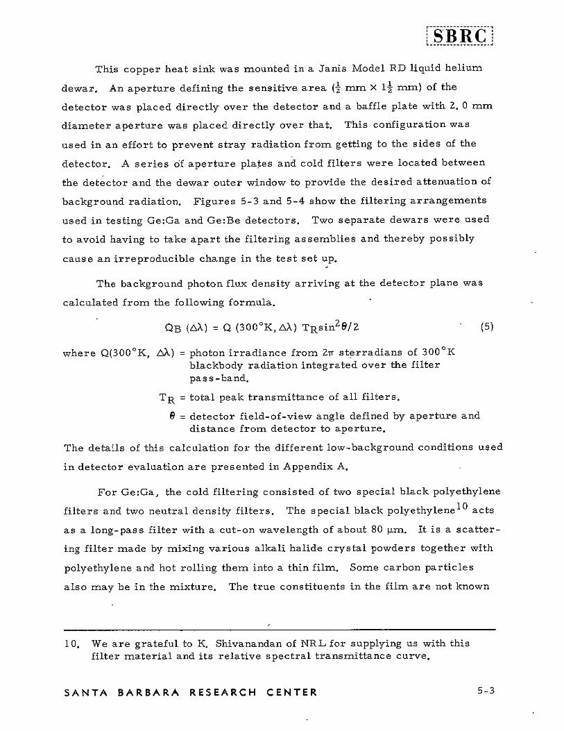
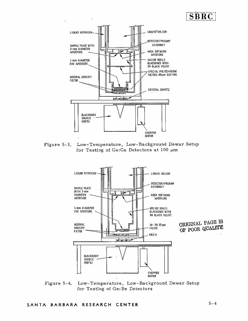
SBRC
-_LIQUID NIT(ROGEN LIQU ID-HEL IUM
DETECTOR IPREAMP
BAFFLE PLATE WITHbullram DIAME~TER L -ASSEMBLY
APERTURE AREA DEFINING APERTURE
1mm DIAMETER --- -INSIDE WALLS
FOV APERTURE BLACKENED WITH 3M BLACK VELVET
NEUTRAL DENSITY 7 SPECIAL POLYETHYLENE FILTERS IBOpmCUT-ON)
FILTER
u _ CRYSTAL QUARTZ
BILACKBODY SOURCE (5OOdegK)
CHOPPER MOTOR
Figure 5-3 Low-Temperature Low-Background Dewar Setup for Testing of GeGa Detectors at 100 jim
LIQUID NITROGEN LIQUID HELIUM
DETECTORPREAMP
ASSEMBLYBAFFLE PLATE WITH 2-rm DIAMETER AREA DEFINING APERTURE APERTURE
-mm DIAMETER INS IDEWAL FOV APERTURE BLACKENED WITH
3M BLACK VELVET
NEUTRAL 16- TO 22Nm ORIGINAL PAGE IS DEN4SIT FITR-ooVA FILTER KRS-5 OF POOR
dBLACKBODYSOURCE (SOK)
CHOPPERMOTOR
Figure 5-4 Low-Temperature Low-Background Dewar Setup for Testing of GeBe Detectors
5-4SANTA BARBARA RESEARCH CENTER
SBRC to us The neutral density filters were made at SBRC by evaporating a thinshy
nichrome metal film onto z-cut crystal quartz flats The relative spectral
transmittance of these filters was not measured but was assumed to be
essentially flat in the 60- to IZ0-gLm range The average transmittance of
these filters was checked at room temperature by placing each filter in
front of a dewar containing a GeGa detector (also filtered to detect only
radiation beyond about 60 4m) and measuring the attenuation of the detector
signal from the 500 0 K blackbody source
In most of the GeGa detector testing done on this program a filter
combination was used which gave a calculated background flux QB = I 2 X 10⁹
photonscm 2 sec at the detector plane Measurements on one detector were
made at other background flux levels which were obtained by changing the
neutral density filters and field-of-view (FOV) aperture
For GeBe detector testing a combination of a 16- to 22-gm multilayer
interference band-pass filter I and two neutral density filters was used In
this case the neutral density filters were made by evaporating nichrome
metal onto germanium flats This filtering combination had worked well for
testing doped Si detectors in past work at SBRC and was easy to implement
for the GeBe detectors Admittedly it would be more desirable to test
these detectors in the 30- to 50-4m range however a suitable combination
of filters for this range was not readily available so the 16- to ZZ-gm range
was used instead Extrapolation of NEP data from the 16- to 22-grn range
to 50 jim can be made with little additional expected error The filter comshy
bination used for GeBe detector testing gave a calculated background photon
flux at the detector of QB = 9 X 10⁸ photonscm 2 sec
11 Obtained from Optical Coating Laboratories Inc
SANTA BARBARA RESEARCH CENTER 5-5
-SBRC The signal radiation was obtained from a 500K blackbody located in
close proximity to the dewar outer window A variable speed chopped proshy
vided modulation frequencies from 1 to 1000 Hz The blackbody has a large
opening and the detector looks into this opening through the small FOV
defining aperture located within the dewar Therefore the blackbody radiashy
tion is effectively emanating from this aperture rather than from the blackshy
body cavity itself The blackbody signal irradiance at the detector plane
is given by the formula
HBB (AX) = WBB(AX) ABB TRF (6)Tr DZ
where WBB(AX) = blackbody radiant emittance integrated over filter passband
ABB = FOV defining aperture area
TR = total filter transmittance
F = chopper form factor
D = aperture to detector distance
The signal irradiance on the detector is due to the temperature difference
between the 500 0 K blackbody cavity and the room temperature chopper blade
(assumed to be at 300 0 K) Therefore the signal photon flux density impinging
on the detector is greater than the 300K background photon flux density For
noise measurements the blackbody opening is covered with a shutter so that
the detector then only sees 300K background photons
The blackbody radiant emittance was numerically integrated over the
filter pass-band to obtain that fraction WBB(AX) which would pass through
the filter The details of this calculation are given in Appendix B
The chopper form factor is used to convert peak-to-peak signal
irradiance values to root-mean-square values For the chopper used this
factor had a value of 0 40 A listing of all the parameter values used in
Equations (5) and (6) are given in Table 5-1
SANTA BARBARA RESEARCH CENTER 5-6
Table 5-1 List of Parameters Used in Blackbody Irradiance Calculations
Parameter Units GeGa Ge Be
WBB(AX) wcm Z 3 29 X 10-4 1 53 X 10- Z
-3 - 3ABB cmZ 7 85 x i0 1 96 X 10
TR 181 X 10- 4 1 0 X 10- 4
D cm 8 59 6 65
F 040 040 - IZHBB(AX) w(rms)cm2 8 05 X I0- 13 8 6 x 10
o degrees 067 043
QB(3000 AX) photonssec cmz 149 X 1017 636 x 1017
QB(AX) photonssec cmz 1 Z X i09 0 9 X 10⁹
TEST PROCEDURE
All testing was done in a screen room Tests were performed using a
source follower cryogenic preamplifier and the external circuit components
shown in Figure 5-5 The preamplifier output was coupled to a Quan Tech
Model 206C amplifier which provided a voltage gain of 103 Amplifier
frequency response was flat between IHz and 100 kHz The low-frequency
gain was -3 db at 05 Hz Signal and noise readings were taken on a Quan
Tech Model 304 Wave Analyzer and also visually monitored on an oscilloscope
Tests were designed with the object of evaluating detector performance
as a function of frequency voltage and temperature Data were taken at
0 50 K increments from about 4 50 K down to Z00 K Temperatures below
4 ZK were obtained by pumping over the liquid helium reservoir of the Janis
Dewar A calibrated carbon resistance thermometer mounted in a hole
drilled into the copper heat sink shown in Figure 5-Z was used to monitor
detector temperature
ORIGINAL PAGE IS
SANTA BARBARA RESEARCH CENTER OF POOR QUALITYl 5-7
LsBRCJ S DRAIN
lLOAD ---
RESISTORI I l
QUAN TECHWAVE
IANALYZER
IL I DETECTOR C_ _26~ t MFIER-LOSCILLOSCOPE
SOURCE RES ISTOR
Figure 5-5 Diagram of Circuit Used for GeGa and GeBe Detector Tests
Note Circuit elements within dashed line are at cold temperature those outside are at room temperature
Detector bias was first optimized at the highest operating temperature
which gave a reasonable signal-to-noise (SIN) ratio This was usually
around 4 00 K The temperature was then reduced in 0 5 0 increments At
each new temperature setting signal noise and resistance measurements
were taken at 10 Hz with optimum bias At 3 0degK and 00 K a more detailed
look at detector performance was made At these temperatures the measureshy
ments made were 1) zero bias noise versus frequency Z) signal and noise
versus bias at 10 Hz and 3) signal and noise versus frequency at optimum
bias
RESULTS - GeGa DETECTORS
Three GeGa detectors were fabricated and tested during this program
All were made with material from crystal GeGa 4 Detector 4-lbl-1 showed
optimum SN ratio when operated at a bias voltage of 0 035 volt (0 7 voltcm)
while detectors 4-3b1-i and 4-5bl-I had an optimum bias of 0 0Z4 volt
SANTA BARBARA RESEARCH CENTER 5-8
SBRC
(0 5 voltcm) Detectors 4-lbl-l and 4-361-1 were tested only at one
background flux level namely 1 Z X 10 9 photonsseccm Z Detector 4-5bl-l
was tested at various different background flux levels Figures 5-6 through
5-13 illustrate the relationship between bias voltage resistance signal
noise and NEP of these detectors
The resistance versus temperature data in Figure 5-6 show the same
characteristics as were seen earlier in Figure 3-7 That is detector
4-lbl-l has a lower resistance at any given temperature than either 4-3b1-i
or 4-5bl-i This is due to a lower concentration of compensating donor
impurities in this part of the crystal
Detector 4-5b1-l shows an increase in resistance with decreasing
background flux however the magnitude of this increase is less than expected
Since QB was decreased by a factor of 3 2 detector resistance should have
increased by this factor Instead it only increased by a factor of 1 6 From
this result it might be inferred that the calculated background flux level of
3 7 X 10 8 photonsseccm 2 was in error This could possibly have been the
case However it also should be pointed out that there can be a substantial
error in the resistance measurements reported in Figure 5-6 These are
made by an indirect method through the source follower MOSFET circuit
Appendix B describes this method Also the temperature measurements
could be in error due to the fact that the temperature sensing resistor is not
located on the detector but is some distance away in the copper heat sink
Figure 5-7 shows the detector behavior as a function of bias voltage at
two different temperatures Z 0 and 3 00 K Note that at 3 00 the signal
voltage tends to saturate at higher bias This could be caused by either of
two things 1) the drop in detector ac resistance as bias voltage is increased
or 2) photoconductive gain saturation due to carrier sweep-out Signal
saturation was not observed at 2 00 K operation Similar results were found
on two of the three GeGa detectors tested a tendency toward signal saturashy
tion at 3 0degK but no such tendency at 2 0degK This indicates a much lower
free-hole lifetime at 2 00 K operation
SANTA BARBARA RESEARCH CENTER 5-9
------------
a - p
ol
4-3b-I Q bull 12 x109phsC 2m-2
l4-Tbl-L Q8 - 12x 109 ph sc Cmn2
24-5b1-L Q8 37 x108phsec-I cm 9 1144b11 Oi3 seIDSb-O~-12xI I phsC mm
20 25 30 35 40 45 DETECTOR IMTEMPERATURE
Figure 5-6 Resistance Versus Temperature for GeGa Detectors
SIGNAL 1O-
4 loll
010--5- 10
2 A RESISTANCE -~
E
I~NOISE
10-6-0 9
ORIGINAL PAGE IS
NIPN0 OF POOR QALITY
~2degK 3degK
001 00 a 0 D4o 0w 04060 awo DETECTOR tolts)VOLTAGE
Figure 5-7 Signal Noise NEP and DC Resistance Versus Bias Voltage for GeGa Detector No 4-lbl-l at Two Temperatures (10 Hz Data)
SANTA BARBARA RESEARCH CENTER 5-10
The detector resistance decreases with increased bias This is due
primarily to an increase in free carrier density because of an increasing
lifetime with bias
The noise voltage at low bias is predominantly preamplifier noise As
bias voltage is increased detector noise becomes evident
The NEP is higher at low bias voltage because of the preamplifier
contribution to the noise At higher bias it tends to level off This is
typical of most GeGa detectors that have been tested Some however
have shown a clear minimum and then an increasing NEP at higher bias
probably due to an excess detector noise arising at the detector contacts
The detector signal data in Figures 5-8 and 5-9 can be used to calculate
detector responsivity values and from these one can obtain estimates of
quantum efficiency and photoconductive gain The voltage responsivity at
wavelength X is a function of frequency due to the circuit RC rolloff This
frequency dependence can be written as I
Rv(Xf) = Rv(X o) [1 + (ZlfTRRc)Z] - 2 (7)
where Rv(X o) is the dc or low-frequency responsivity and TRC is the circuit
response time By fitting a curve having the functional dependence on
frequency shown by this equation to the signal data in Figures 5-8 and 5-9
it was found that the 1-Hz responsivity values are sufficiently close to the
dc value to be used in an approximate calculation The 1-Hz voltage responshy
sivity was calculated from experimentally measured data using the formula
RVXI)- S (AX) (8)Rv(X 1) = HBB(AnX)ADg
where S(AX) = signal voltage measured at output of preamplifier
HBB(AX) = blackbody irradiance at detector (see Table 5-1) 3
AD = detector area (7 5 X 10 - cm 2 )
g = preamplifier gain (0 85)
SANTA BARBARA RESEARCH CENTER 5-11
4-lbl- 4-3b1-1 4-5b1-l
10-3
- SIGNAL
04
10-5
-6
NOISE
PREAMPLIFIER
8 l10 - i i i l
1 10 100 1000
FREQUENCY (Hz) Figure 5-8 Signal and Noise Versus Frequency for GeGa
Detectors at 3 00 K
Note Background photon flux density was 1 2 X 10⁹ ph sec - I cm - Z
Signal and noise values are referred to the output of the MOSFET preamplifier
SANTA BARBARA RESEARCH CENTER 5-1Z
SBRCI ----- 1--T-T- -r---------TT--------T-shy
10 _
o 10-5
SIGNAL
0 2
10- 7 PREAMPLIFIER
NOISE
4-1bl-1 QB = 12 x 109 ph sec - I cm -shy 4-3b1-1 QB = 12 x 109 ph se-C mshy2
4-5b1-1 QB = 12 x 109 ph sec - I cm- 2
10_8 4-5b1-1 QB = 37 x 108 ph sec - 1 cm shy 2
1 10 100 1000 FREQUENCY (Hz)
Figure 5-9 Signal and Noise Versus Frequency for GeGa Detectors at Z 00 K
Note Background photon flux density was 1 Z X 10 9 ph sec-I cm-Z Signal and noise values are referred to the output of the MOSFET preamplifier
SANTA BARBARA RESEARCH CENTER 5-13
-SB -RC
The short-circuit current responsivity was calculated from the voltage
responsivity using the equation
is(X 1) = Rv(X 1)R (9)11
where R11 is the parallel resistance formed by the load and the detector ac
resistance values
RacRLH11 = Rac + RL (10)
and
[ V dRdc-Rac = Rdc l - - (11)I Rdc dV
According to detector theory the short-circuit current responsivity is given
by
w e= c GP c (lZ)
Lc = photoconductive gain
7 = free-hole lifetime
S= hole mobility
E = electric field strength
L = interelectrode spacing
77 = quantum efficiency
e = electronic charge
X = wavelength
h = Plancks constant
c = speed of light
Therefore once a value for I(X o) is obtained some estimates of values for
17 and Gpc can be made
Using the foregoing equations and the measured experimental data
values of current responsivity were calculated for the three GeGa detectors
The results for operating temperatures of both 2 0 K and 3 00 K are shown
in Table 5-Z The current responsivity values are at the peak of the detectors
SANTA BARBARA RESEARCH CENTER 5-14
i-SBRCj]
Table 5-Z Parameters Used in Calculation of Short-Circuit
Current Responsivity for GeGa Detectors
DETECTOR NUMBER TEMPERATURE PARAMETER UNITS 4 (OK)
4-]b1-1 4-3b1-1 4-5b1-1
BIAS VOLTAGE VOLTS 0035 0024 0024 20 AND 30 ELECTRIC FIELD VOLTSICM 070 048 048 20 AND 30
10 x I010 Rdc OHMS 5 K 109 14 x 10I0 30
Rac OHMS 28x 109 73 x 109 Li x 1010 30
S(AX 1) MILLIVOLTS 044 020 019 30
RV(Ap 1) VOLTSIWATT 86 x i010 39 X 1010 37 x 1010 30
Is(p 1) AMPS WATT 32 (10) 61 41 30
nGpc (0124) 0076 0051 30
Rdc OHMS 16 x 1010 20 x 1010 31 x 1010 20
Rac OHMS 12 x 1010 13 X 1010 24 x 1010 20
S(441) MILLIVOLTS 023 012 015 20
x 1010 Rv(Xpl) VOLTSWATr 4 5 X 10¹⁰ 23 29 x 1010 20
Is(Ap 1) AMPSWAnT 46 22 18 20
flGpc 0057 0021 0022 20
RL - 5 x 10¹⁰ (NOMINAL VALUE)
Xp = 100 Pm 0hAT VAGE IS
AD - 7 5 x 10⁻³ cm2 (15 x 05 mm) ORUGNL- ALI OF pOOR Q
f =IHz
pm An exceptionallyspectral response curve which was taken to be 100
0 high value of current responsivity was obtained for detector 4-lbl-l at 3 O K
No obvious experimental error could be found in the data however the result
does seem to be spurious By comparison of the Z 00 and 3 00 K current
value around 10responsivities of the other two detectors it appears that a
ampswatt would be more appropriate for this detector The current
responsivity for this detector would be expected to be somewhat higher than
the others because of a higher applied bias and longer free carrier lifetime
Both ofthese conditions lead to a higher photoconductive gain for this detector
The signal versus bias voltage data shown previously in Figure 5-7 indicate
that the photoconductive gain could be on the order of 0 5 (This result is
of course based on the assumption that the maximum value of the gain at
saturation is 0 5 ) The use of these results in Equation (12) leads to a
5-15SANTA -BARBARA RESEARCH CENTER
quantum efficiency of 0 Z5 which seems reasonable considering the Ga doping
concentration used in these detectors The other two detectors probably are
operating with a photoconductive gain around 0 Z at 3 O0 K For Z 00 K
operation a decrease in current responsivity by a factor about 2 5 is
observed This must be attributed to a decreased photoconductive gain of
the same amount since the quantum efficiency would not be expected to
change simply because of a change in operating temperature
The measured signal-and-noise data was used to calculate the NEP
data which is shown in Figures 5-10 5-11 and 5-1Z The NEP versus
frequency data shows an essentially flat behavior from 1 to 40 Hz and then
rises slowly An effort was made to measure detector noise data at frequencies
below 1 Hz using a spectrum analyzer The data obtained were unreliable
thus not reported here
The NE versus temperature data of Figure 5-12 show a fairly clear
minimum at 3 00 K operation At higher temperatures NEP increases due to
increasing detector generation-recombination noise and decreasing detector
resistance At lower temperatures the NEPincrease is mainly due to a
decreased detector responsivity The conclusion is that the optimum operatshy
ing temperature is close to 3 00OK NEP values of about 0 7 to 1 X 10-16 1
wattsHz2 were achieved with a background flux of 1 2 X 10⁹ photonsseccm Z
One detector number GeGa 4-5b-i was also measured at various
different background flux levels Figure 5-13 shows a plot of calculated NEP
values versus frequency at four different flux levels At the highest backshy
ground flux NEP rises in the low-frequency range This is due to 1f noise
in the detector At the lower background flux levels NEP shows less
dependence on frequency and is reasonably flat down to 1 Hz - The lowest1
-measured NEP was 4 X 10 - 1 7 wattsHz at I -lz with a background level of
3 7 x 10 8 photonsseccm z
SANTA BARBARA RESEARCH CENTER 5-16
10-15 iI iF ---- I~t T--
T4-lbl-1 QB 12 x 109-E s---f1j2 -I -2
4-3b1-1 QB = 12 x 109 ph sec cm 1 -2
4-5b1-1 QB = L2 x 109 ph sec- cm
QB -37 x 108 ph sec- cm -2 4-5b1-I
1 1 4 - - --- o
1 0 -17 [ 1 1 1 1 1 I1 1 1 II I
1I0 100 1000
FREQUENCY (Hz)
Figure 5-10 NEF Versus Frequency for GeGa Detectors at 3 OdegK
10-1
I -2 4-Ibi-1 QB - 12 x 109 ph sec cm
I -2 4-3bl-1 QB = 12 x 109 ph sec cm
I 24-5bl-1 Q8 12 x 109 ph sec Cm
- 2 4-56l1-I 37 x 108 phsec 1 cmQB shy
__ 1
iiiI fl LLII I it
1 10 100 1000
FREQUENCY (Hz)
Figure 5-11 NEP Versus Frequency for GeGa Detectors at Z00 K
SANTA BARBARA RESEARCH CENTER 5-17
iSBRC]
4-1E- OB 1]2 x ]09 ph sle c 2
4-31-L Q8 L2 X109ph se-t cm-2 4-b1-1 QB - 12 x 109 phse 1 cm 2
4-5b1-L QBshy3 7 X10⁸ ph seC1 cm -2
t
I IT
-----I
1WI71
20 25 30 3r5 4 0 4 5
TEMPERATURE(K1
Figure 5-1Z NEP Versus Temperature for GeGa Detectors at a Frequency of 10 Hz
SQB- 124 x 109 phseccm2
QR 3 7 x 10⁸ phlseclcm2
Q8 = 175 x 1010 phlseccm 2
BQ 117 x j112 phseclcm2
10_14 _________ ________ _______
- NOTE SCALE CHANGE
S --shy _-shy
1 10 100 1000
FREQUENCY (Hz)
Figure 5-13 NEP Versus Frequency for GeGa Detector 4-5b-I at 3 00 K for Four Different
Background Flux Levels
SANTA BARBARA RESEARCH CENTER 5-18
r ---------------SBRC
RESULTS - GeBe DETECTORS
As mentioned previously all three GeBe detectors fabricated and
tested on this program were cut from the same slice of crystal Ge Be 10
The slice number was 3a and the location of this slice in the crystal was
adjacent to slice 3 from which the Hall sample was taken The Be doping
1 3 X 10 1 5 concentration was atomscm 3 Figures 5-14 through 5-Z0
illustrate the relationship between bias voltage resistance signal noise
and NEP of these detectors lt
In Figure 5-14 the signal is seen to be a linear function of bias voltage
and does not tend to saturate as did the GeGa detectors The resistance is
seen to be nearly constant with bias voltage to it can be assumed that Rac
is equal to Rdc The NEP is higher at low bias due to preamplifier noise
and then decreases tending to flatten out as bias increases This is quite
evident at Z 00 K operation but for this particular detector at 3 00 K the
NEP starts rising prematurely due to excess detector noise The other
detectors tested showed the flatter NEP curve at both operating temperatures
Figure 5-15 shows the measured resistance versus temperature data
The detectors all have similar resistance values as would be expected for
detectors cut from the same slice of material Since this material did not
show significant hopping conductivity the resistance is background photon
limited at the lowest temperatures with a value of Z 5 X 10 1 0 ohms This
resistance value is substantially lower than might be expected based on a
theoretical calculation The background limited dc resistance can be
expressed as
Rdc - L cflQBTepiw
(13)
ORIGINAL PAGE IS OF POOR QUALITY
SANTA BARBARA RESEARCH CENTER 5-19
--- S- --- -shy
- ~ SIGIAL
---20K
i0 5 IOU
6I0- -1-
NOISE RESISTANCE
Detector Voltage for CeBe l0-3a-3 at TwoTemperatues 2degK and 3K
-10-33-1 10-3a-2
010-ashy
109
20 2 303540 45s DETECTOR (KT5MPERATURE
Figure 5-15 Resistance Versus Detector Temperature of Ge Be Detectors
Note Background photon flux density was 0 9 X 10 9 ph sec-1 cm-2
SANTA BARBARA RESEARCH CENTER 5-Z0
LSBRC
Inserting the following values into this equation
- ZL = 5 X 10 cm
T7 =03
QB = 9 X 10⁸ photonsseccm Z
i =10 - 7 sec
e = 16 Xl0- 1 9 coul
ii = 4 X 10⁵ crZvolt sec
w = 1 5 y0-1 cm
gives a value for Rdc of 1 9 X i01 ohms nearly an order of magnitude
higher than measured All the above parameters except 71 QB and T came
from direct measurements The 77and T values are reasonable approximations
which should be within a factor of 2 or 3 of the true values It would be
necessary to increase the 77 product by a factor of 10 to bring the calculated
Rdc into agreement with the measured value This seems to be unreasonable
therefore it must be concluded that QB is actually higher than the stated
value of 9 X 10⁸ photonsseccm z
Figures 5-16 and 5-17 show measured signal-and-noise data versus
frequency for two operating temperatures The signal data can be analyzed
in the same way as for the GeGa detectors to obtain short-circuit current
responsivity values and estimates of the 1]Gpc product The results are given
in Table 5-3 The blackbody signal radiation was restricted to the 16- to
22-gim band by a filter Therefore direct use of Equation (8) gives the
voltage responsivity at a wavelength of -about 19 pLm To convert this value
to responsivity at the peak of the GeBe spectral response which is at 40 pLm
the calculated responsivity was multiplied by a factor of 2 This factor is
based on the relative spectral response of GeBe reported by Shenker et al 12
All the values of voltage and current responsivity listed in Table 5-3 are at
the detectors peak wavelength of 40 pLm The calculated current responsivity
values are seen to be in the neighborhood of 2-5 ampwatt DetectorGeBe 10-3a-3
1Z See Reference 5
SANTA BARBARA RESEARCH CENTER 5-21
tllm I - r rt irn I ITII41
10-3a-1 10-3a-2 10-3a-3
10-3 N
SIGNAL
10shy4
J4______
-
C
10-5
CNOISE
PREAMPLIFIER NOISE 10-7 shy
-RIGINAL PAGE IS OF POOR QUALTY
1 10 100 1000 FREQUENCY (Hz)
Figure 5-16 Signal and Noise Versus Frequency for GeBe Detectors at 3 00 K
Note Background photon flux density was 0 9 X 1-09 ph sec- 1 cm-Z Signal and noise values are referred to the output of -the MOSFET preamplifier
5-ZZSANTA BARBARA RESEARCH CENTER
l II IIIII~~~SR
-L1B3ashy
10-3a-1 - ------10-3a-2 --- 10-3a-3
10- 41______ __
10-4
a V SIGNAL
-shy4
PREAMPLIF IERNOS
- 810 1 a I l i l t I J l
1I0 100 1000
FREQUENCY (Hz)
Figure 5-17 Signal and Noise Versus Frequency for GeBe Detectors at 2 OdegK
Note Background photon flux density was 0 9 X 10 9 ph sec-i crn-Z
Signal and noise values are referred to the output of the
MOSFET preamplifier
SANTA BARBARA RESEARCH CENTER 5-23
SBRC L -
Table 5-3 Parameters Used-in Calculation of Short-Circuit Current Responsivity for GeBe Detectors
UN ITS DETECTOR NUMBER TEMPERATUREPARAMETER 10-3a-3 (OK)10-3a-1 1O-3n-2
BIAS VOLTAGE VOLTS 0235 0235 0082 30 ELECTRIC FIELD VOLTSICM 470 470 164 30
Rac OHMS 19 x 1010 22 x 1010 18 x 1010 30 S(AX 1) MILLIVOLTS 18 19 056 30
Rv(Xp 1) VOLTS(WAT 66 x 1010 69 x 1010 20 x 1010 30
Is(Xp 1) AMPSWAIT 57 54 18 30
flGpc 0176 0167 0056 30
BIAS VOLTAGE VOLTS 0259 0353 0188 20
ELECTRIC FIELD VOLTSICM 519 705 376 20
Rac OHMS 22 x 1010 26 x 1010 27 x 1010 20
S(AX 1) MILLIVOLTS 15 11 11 20
Rv(Ar 1) VOLTSIWAIT 55 x 1010 40 x1010 40 x 1010 20
Is(Xp 1) AMPSIWATT 43 29 28 20
1GPC 0133 0090 0081 20
RL =3 x 10¹⁰ OHMS (NOMINAL VALUE)
Ap = 40 pm AD 75 x 10-3 cm2 15 x 05 mm)
I =1 Hz
was somewhat lower than the other two because it had to be operated at a
lower bias voltage If one assumes a quantum efficiency of 0 3 then the
photoconductive gains would be in the range of 0 2 to 0 6 These are
reasonably values for the low-frequency gain (I Hz) which would not be
limited by carrier sweep-out
Calculated NEP values are plotted versus frequency and temperature
in Figures 5-18 5-19 and 5-20 Figures 5-18 and 5-19 show the NEP to be
essentially flat with frequency between I and 10 Hz and then rising for higher
frequencies An exception is Detector GeBe 10-3a-Z which appears to have
some excess noise in the I- to 2-Hz range causing an increased NEP at these
low frequencies
5-24SANTA BARBARA RESEARCH CENTER
ISBRCI
-10-14
10-3a-I 10-3a-2 -
S 10-3a-3shy
-15 10 shy
IO-16 l
1 10 100 1000 FREQUENCY (Hz)
Figure 5-1-8 NEP Versus Frequency for GeBe Detectors at 3 00 K
- I - Z Note Background photon flux density was 9 X 10⁸ ph sec cm
10-14 j1n --- 1 i-- r- r r rr
1O-3a-1 110-3a-2
- -- 10-3a-3
0-1
1o-16 ORIGINAL PAGE IS OF POOR QUALITY
- 1 7 10 1 1 1 1 I Ii t - 1 -1 1 t 1I I l
1 10 100 100
FREQUENCY (Hz)
Figure 5-19 NEP Versus Frequency for GeBe Detectors at 2 00 K
- -z Note Background photon flux density was 9 X 10⁸ ph sec I cm
SANTA BARBARA RESEARCH CENTER 5-Z5
SBRCI
The NEP versus temperature data in Figure 5-Z0 showa reasonably
flat behavior between Z 0 and 3 00 K and then rise at higher temperature
An exception here is detector GeBe l0-3a-3 which reaches its lowest NEP
only at Z 00 K This ditector had to be operated at a lower bias voltage than
the others because it became excessively noisey at higher bias This
problem was most likely due to contact noise The minimum NEP is about
the same for all three detectors and is Z to 3 X10⁻¹ 6 wattsHz2
10-3a-I 10-3a-2 10-3a-3
15 10shy
=
-10 16 1 I 1 3 1 I 20 25 30 35 40 45
DETECTOR TEMPERATURE (OK)
Figure5-ZO NEP Versus Detector Temperature for GeBe Detectors
Note Background photon flux density was 9 X 10 8 ph sec-1 cm-Z
SANTA BARBARA RESEARCH CENTER 5-26
Section 6
CONCLUSIONS AND RECOMMENDATIONS FOR FUTURE WORK
This work has provided significant advancements in the technology of
GeGa and GeBe photoconductive detectors for use in astronomical observashy
tions at wavelengths from 30- to 1Z0-gm All the major goals for this phase
of the development were accomplished The primary conclusions that can
be drawn from the work performed thus far are as follows
GeGa DETECTORS
A Ge purification method was developed which reduces the residual
donor impurity concentration to the 1010 atomscm 3 range Residual
acceptor impurity content may be much higher but is inconsequential
to detector performance
shown to produce Introduction of Ga by the zone leveling method was
uniformly doped ingot with sufficient material for fabrication ofa many detectors The doping concentration can be controlled within
an acceptable tolerance
Crystals doped to Z 5 X 10¹⁴ Ga atomscm 3 do not show hopping
conductivity Higher doping concentrations might be useful for
increasing the detectors quantum efficiency
Short-circuit current responsivity for 100 gm radiation was measured
to be in the range of 6 to 10 ampswatt at 3 0 0 K operation This
implies an 77Gpc product of 0 074 - 0 IZ4 Quantum efficiency was
estimated to be around 0 25
Detectors were not enclosed in an integrating cavity The use of
such a scheme 1could significantly improve quantum efficiency
An NEP of 4 X 10-17 wattsHz2 was measured at 1 Hz with a backshy
ground flux of 3 7 X 10⁸ photonsseccm Z at 3 00K operating
temperature This comparesfavorably with the calculated BLIP
value of 1 X10-17 wattsHz2 (77 =-0 30 Xp = 100 gm)
The NEP is minimized at an operating temperature very close to
3 0degK Higher or lower operating ter-peratures may cause a
degradation of NEP
Reproducibility and yield of good detector elements were excellent for
GeGa detectors Most of the technology development on this material
has been completed and the producibility of detectors which meet or
exceed the NEP objectives for the IRAS mission has been demonstrated
SANTA BARBARA RESEARCH CENTER 6-1
SBRC
GeBe DETECTORS
Oxygen must be eliminated during growth of GeBe crystals to prevent Be-O complexing A vacuum zone melting process was developed which provided a method for doing this
10 1 5 The Be concentration should be kept below Z X atomscm 3 to prevent impurity hopping conductivity from seriously lowering detector resistance at 3 00 K
The electric field strength that can be applied to uncompensated GeBe is limited to less than 10vcm due to impact ionization of shallow acceptor levels
o Short-circuit current responsivity for 40 pLm radiation was measured
to be in the range of Z to 5 ampswatt for 3 00 K operation
Detectors were not enclosed in an integrating cavity The use of such a scheme could significantly improve quantum efficiency
- 1 6 O The lowest measured NEP for GeBe detectors was 2 to 3 X 10
wattsHz I
at a frequency of I Hz with a background flux of 9 X 10⁸
photonsseccm 2 The BLIP value for this background is 4 6 x( i017 wattsHzi (7 = 0 3 Xp = 40 ptm)
The NEP is optimized at 3 00 K or lower There was no clear indication of a minimum in the NEP versus temperature plot
The yield of GeBe detectors from a given slice of material was acceptable Two out of three detectors fabricated and tested had reasonably good performance the third had excessive 1f noise
The uniformity of GeBe material properties within a slice is excellent Uniformity over a whole ingot has not yet been achieved
The producibility of GeBe detector elements is presently limited by the crystal material uniformity and quality
RECOMMENDATIONS FOR FUTURE WORK
In the case of GeGa recommendations for future work could be called
minor technological improvements The work accomplished to date has
shown that GeGa detectors can meet the objectives of the IRAS mission
However minor improvements might still be achieved For example
GeGa crystals with a Ga concentration greater than Z 5 X 10¹⁴ atomscm 3
should be grown and evaluated to see if the quantum efficiency can be
improved Also the use of integrating cavities for improvement of quantum
efficiency should be investigated
SANTA BARBARA RESEARCH CENTER 6-2
Measurements of detector behavior at frequencies below I Hz should
be made Although data taken to date show no evidence of any problem in
this frequency range confirming measurements should be made
In the case of GeBe the crystal growth technology needs further
improvement It is recommended that more work be done in two areas
First the method of zone leveling to produce a uniform Be concentration
along the whole ingot should be implemented With the existing method
variation of Be concentration along an ingot is still too great to give a
sufficient quantity of material for focal plane array production Secondly
crystals of compensated material should be grown and evaluated to see if they
have any advantage over the uncompensated material which has been used
in past work The uncompensated material must be operated at low electric
field strengths to prevent impact ionization of the shallow acceptors In
compensated material electric field strengths 4 to 5 times larger should
be permissible This could give an improvement in photoconductive gain
provided that the hole lifetime is not seriously degraded by the additional
compensating donors Careful control will be needed to avoid introduction
of too manV compensating donors
As mentioned for the case of GeGa detectors the use of integrating
cavities should also be investigated for GeBe detectors Finally measureshy
ments of detector behavior at frequencies below I Hz should also be made
SANTA BARBARA RESEARCH CENTER 6-3
-SBRC-
Appendix A
IRRADIANCE CALCULATIONS
This appendixpresents details of the calculation of blackbody signal
irradiance and background photon flux density at the detector focal plane in
the low-background test dewars
GeGa TEST DEWAR
As mentioned in Section 5 in the main text the GeGa detectors were
tested using a long-wavelength pass filter consisting of two pieces of special
black polyethylene and crystal quartz These materials along with the
detectors natural cutoff at about 120 pLm produced a relative spectral response
as shown in Figure A-1 This isolated a spectral band about 35 pLm wide
in the 100-pim region Neutral density filters were also used to further
attenuate the background photon flux on the detector
The effective blackbody signal irradiance on the detector was calculated
by numerically integrating the blackbody flux over the filter spectral range
To do this the spectral range was broken up into intervals each 5 pLm wide
as shown in Figure A-1 The blackbody radiant emittance for each spectral
interval was then obtained from a radiation slide rule These values are
shown in Table A-1 along with the spectral intervals and the relative filter
transmittance in each spectral interval Since the signal radiation is
produced by the difference between the 500K blackbody and a 300 0 K chopper
blade these values were obtained from the slide rule and one was subtracted
from the other to obtain the actual signal radiant emittance in each interval
The difference values are listed in column 5 of the table Multiplication of
each number in column 5 by the corresponding -relative filter transmittance
SBRC is indebted to K Shivanandan of NRL for furnishing these data
SANTA BARBARA RESEARCH CENTER A-1
10
09
r
I
-n
L
08 r
07
L
06 I
Co
c4 05
LO
II I 04
03 I
r
-IL
I
I
II
02 SI I
01
I
0 50
I
60
Figure A-I
I
70 80 90 100 110 120 WAVELENGTH (pm)
Relative Spectral Response of GeGa Detector with Long Wavelength Pass Filter
I
i
130
SANTA BARBARA RESEARCH CENTER A-Z
V) Table A-i Listing by Spectral Interval of Blackbody Signal Radiant Emittance and gt Background Photon Flux Values Used for GeGa Detector Testing z -i
(1) (2) (3) (4) (5) (6) (7) (8) w (X)gt RF(X) W500(A) W300(X) W500(X) -W300(X) WBB(A) Q30O QB(X)
4m) (wcm2) (wlcm2) (wcm2) (wcm2) (phseccm2) (phseccm2)
x1O3 x1O-3 xlO- 3 xO-5 xl017 x 016
S40-45 0 1436 0670 0766 0 1430 P
m 45-50 0 0912 0444 0468 0 1060 0
r 50-55 0 070 0 632 0310 0322 2254 0818 057
gt 55-60 0125 0454 0230 0224 2800 0664 083
60-65 0165 0334 -0172 0162 2673 0540 089
65-70 0260 0248 0130 0118 3068 0441 115
m 70-75 0320 0190 0100 0090 2880 0364 117 z 75-80 0375 0150 0080 0070 2625 0312 117
0257 150 m
80-85 0585 0118 0062 0056 3276
85-90 0685 0094 0050 0044 3014 0220 151
90-95 0810 0076 0040 0036 2916 0186 151
00 95-100 0950 0058 0032 0026 2470 0157 149
00 100-105 0900 0050 0028 0022 1980 0144 130
0105-110 0750 0040 0020 0020 1500 0108 081
0102 061110-115 0600 0032 0018 0014 0840
115-120 0350 oo 0016 ~ WB(X 3o_910-4ooo 0030 ~ oooo0014 0490 0094 033
120-125 0100 0027 0014 0013 0130 0086 009 ~~~
QB( 300AX) =149 x 1017SUMMATION WBA)=32x0
ISBRC
in column Z gives the effective blackbody radiant emittance in each spectral
interval These values are listed in column 6 Summation overall spectral
intervals then gives the total blackbody radiant emittance in the filter pass band
This total radiant emittance number is then used in Equation (6) to
calculate the irradiance at the detector focal plane Also needed for this
calculation are the absolute peak transmittance values for each filter and
the dewar window These are as follows
Absolute Peak Transmittance
1 Quartz window 0 85 First neutral density filter 0 015 Second neutral density filter 0 06 Z Special black polyethylene filters (0 5Z) Z
Atmospheric water vapor 0 88
Total transmittance TR = 1 8 X 10- 4
A transmittance factor for atmospheric water vapor was also included
Although this produces a small effect on total transmittance it was found to
be not negligible The effect of atmospheric absorption was checked by
flushing the space between the blackbody opening and the dewar window with
dry nitrogen This produced an increase in a GeGa detectors signal by 13
Since it was impractical to continue flushing this space during all tests
the atmospheric correction factor was applied to the blackbody irradiance
calculation
The equation for signal irradiance Equation (6) in Section 5 was
written as WB(ZX)AB TR F
HBB(AX) = WBB(AX) BB (AI) SN DZ
A-4SANTA BARBARA RESEARCH CENTER
Substituting the values calculated above along with those other values listed
in Table 5-I gives
HBB(AX) _ (3 29 x 10-4)(7 85 X 10-3)(1 8 x 10⁻⁴)(0 4) - o xI - 13 wcm 2 (3 14) (8 59) Z
The background photon flux density at the detector plane was calculated
in a similar manner Column 7 of Table A-I lists 300 0 K photon flux density
values for each spectral interval as obtained from a radiation slide rule
Column 8 gives the effective values passing through the filter (column Z X 7)
and their sum over all the spectral intervals
Equation (5) in Section 5 was then used to calculate the background
photon flux density at the detector plane This equation is
QB(AX) = Q(300 0 K AX) TR sinz 82 (AZ)
The filter transmittance factor in this case does not include the outer
warm quartz window nor does it include the atmospheric water vapor loss
It includes just the two neutral density filters and the two special polyethylene
filters Thus TR = 2 4 X 10- 4 Using this value along with the appropriate
values from Tables A-I and 5-1 gives
BX) = (149 X 1017)(Z 4 X 10-48 59) = 1 Z X 109 phseccm z
CeBe TEST DEWAR
The GeBe Detectors were tested using a 16- to 2Z-vrn multilayer bandshy
pass filter plus neutral density filters on germanium The relative transshy
mittance curve for this band-pass filter is shown in Figure A-2 The blackshy
body signal irradiance through this filter was calculated by numerical
integration in the same manner as was described for the case of GeGa
Table A-Z lists the relevant data
sectRGIN AL
SANTA BARBARA RESEARCH CENTER A-5
09
08 I I I
II I IL I I I I
06-C
04 I I
03shy
02
01 I
15 16 17 18 19 20 21 22 23 24
WAVELENGTH (um)
Figure A-Z Relative Spectral Response with Band-Pass Filter
of GeBe Detector
A-6SANTA BARBARA RESEARCH CENTER OO 0 A-6uA yOF P00R
z -I wgt
gt
X
Table A-Z Listing by Spectral Interval of Blackbody Signal Radiant Emittance Background Photon Flux Values Used for GeBe Detector Testing
and
gt
m
(1)
X 10m)
(2)
RF(X)
(3)
W5go(X) (wlcm2)
(4)
W30j(X) (wlcm2 )
(5)
W500) - W30 ijX) (wcm2)
(6)
WBB(A) (wlcm2)
(7)
Q3 0(X) (phlseccm2)
(8)
QB(X) (phseccm2)
m gtx
0 -
m Z -1 m1
15-16 16-17
17-18 18-19
19-20
20-21
21-22
22-23
23-24
005 080
078 091
086
072
045
037
015
770 630
525 455
385
350
280
245
210
x I0-
220
175
152 138
129
110
097
087
074
x Io-3
550
455
373 317
256
240
183
158
136
x io-3
028
364
291 289
220
173
082
058
020
x i017
156
144
140 131
123
115
1-03
098
090
xI017
008
115
109 119
106
083
046
036
014
SUMMATION WBB(AX) 153 x 10-2 QB3 0QAX) 63 1017
0
4 lo
-SB-R--
Using the data from Tables A-Z and 5-I and substituting into Equation
(A l) gives
HBB(UX) = (1 53 X 1 0 -Z)(1 96 X 10-3)(1 0 X i0-4)(0 4) = 8 6 X 10 - I Z wcm Z (3 14) (6 65) Z
The background photon flux density at the detector was obtained by subshy
stituting data from Tables A-1 and 5-1 into Equation (AZ) to get
QB(300K A) = (6 36 x 1017)(1 0 X 10 -6 65) = 9 0 X 108 phseccm Z
DETECTOR RESPONSIVITY
The blackbody signal irradiance values calculated in this appendix were
used to obtain detector responsivity by the usual formula
V9(AX) (M) Rv(A) - HBB(AX) AD
where Rv(X) is the responsivity in voltswatt VS(AX) is the measured signal
voltage AD is the detector sensitive area and HBB(AX) is the effective signal
irradiance It turns out that this procedure yields the responsivity at the
peak of the filter spectral distribution Xp A derivation of this result is as
follows
If Rv(X) is the detector responsivity at any wavelength and Pgt is the
signal power per unit of wavelength (wattsnLm) on the detector at this waveshy
length then for a given wavelength range between X and XZ the detector
signal voltage will be given by Xz
Vs(AX) = f Rv(X) PX dX (A4) X 1
where AX refers to the spectral interval X1 - XZ
SANTA BARBARA RESEARCH CENTER A-8
L[SBRCJ
If the detectors Rv(X) curve is expressed as a relative response
normalized to unity as shown in Figures A-I and A-Z then equation (A4)
can be written as Xz
VS(AX) = Rv(Xp) f RR(X) PX dX (A5)
where RR(X) is the relative response ( 1 at Xp) and Rv(Xp) is the responsivity
at X p This equation can be rewritten as
Rv(Xp) = XV (A6)
j RR(X) PX d xl
The integral in the denominator is the same as HBB(AX) AD when
HBB(AX) is calculated by the numerical integration method described
previously in this Appendix Therefore the responsivity calculated from
equation (A3) is the responsivity at the peak of the relative spectral response
curve Xp
SANTA BARBARA RESEARCH CENTER A-9
Appendix B
DETECTOR RESISTANCE MEASUREMENTS THROUGH MOSFET
This appendix describes the method used for determining detector
resistance values when the detector is connected to the cryogenic MOSFET
source follower preamplifier
The circuit diagram is shown in Figure B- i The detector dc resistance
is given by
Rdc = VDI (B1)
where
I = VB(RL + Rdc) (BZ)
The voltage drop across the detector VD will appear at the MOSFET source
terminal multiplied by the gain of the source follower This voltage is
measured by observing the change in V S as the detector bias voltage is
switched from zero to ON Thus
V D = AVs0 85 (B3)
where LV S is the observed charge in source voltage and 0 85 is the source
follower gain Combining equations (BI) (BZ) and (B3) gives
Rdc RL ((B4)(085 yv) -1
Use of this equation requires prior knowledge of the load resistance
RL Since the load resistance value can vary with temperature and bias
voltage this may introduce considerable error into the determination of
Rdc by this method Values of VB and AVs can be measured with good
precision and will not produce a large error
SANTA BARBARA RESEARCH CENTER B-I
- ------------
VB I
LOAD I RESISTOR RL
DVs
DETECTOR I- Rdc I
L----- --
VB = BIAS VOLTAGE APPLIED EXTERNALLY ACROSS BOTH DETECTOR AND LOAD
= VOLTAGE DROP ACROSS DETECTORVD
VS = SOURCE VOLTAGE
Figure B-I Circuit Diagram for Low-Background Detector Testing
Table B-i shows measured resistance values versus temperature and
applied voltage for a typical load resistor used in the detector assemblies
delivered on this program It is clear from these data that good calibration
of the load resistor must be accomplished to obtain accurate values for
Rdc from equation (B4)
Table B-I Resistance Versus Temperature of Typical Load
Resistor Used in IRAS Device Assemblies
Resistance (Q) Resistance (Q) Resistance ()Temperature at at at
(K) OZO V 0zoo V Z00 V
I0 1 04 Z 3 8 X 10¹⁰ 3 7 x Z 7 X 10¹⁰
4 0 3 7 X 10¹⁰ 3 9 X 10¹⁰ 28 X 101 0
0 4 7 X 10 1 0 1 03 5 44 X10 1 3 2 X10
03 0 5 1 x I0 6 0 x I010 3 7 X 10 1 0
ORIGINAL PAGE 18 B-Z
SANTA BARBARA RESEARCH CENTER OF POOR QUALITY
Another obvious method for determining Rdc would be to attach an
additional wire to the detector at the connection to the MOSFET gate and
bring this lead out of the dewar Measurements of detector current and
voltage could then be made directly However tw6 problems arise with
this method First the additional lead to the detector produces an added
capacitance at the gate input which will cause the circuit response to roll
off at lower frequencies Since the combination of MOSFET gate input andshy
detector capacitance is only about 5 pf distributed capacitance from the
additional wire bould easily equal or exceed this value Secondly the
insulation resistance of the dewar feed-throughs has to be very high in fact
much higher than the detector resistance If detector resistance values are
in the 10 1 0 -ohm range the insulator resistance should be greater than i0 1 Z
ohms The metal-glass feed-throughs used on our dewars can have this
high an insulation resistance if properly cleaned and kept dry However
past experience has shown that they are easily contaminated with use and
leakage problems result It was because of these problems that the indirect
method of detector resistance measurement described above was adopted
SANTA BARBARA RESEARCH CENTER B-3
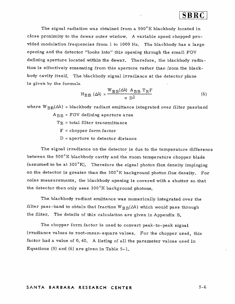
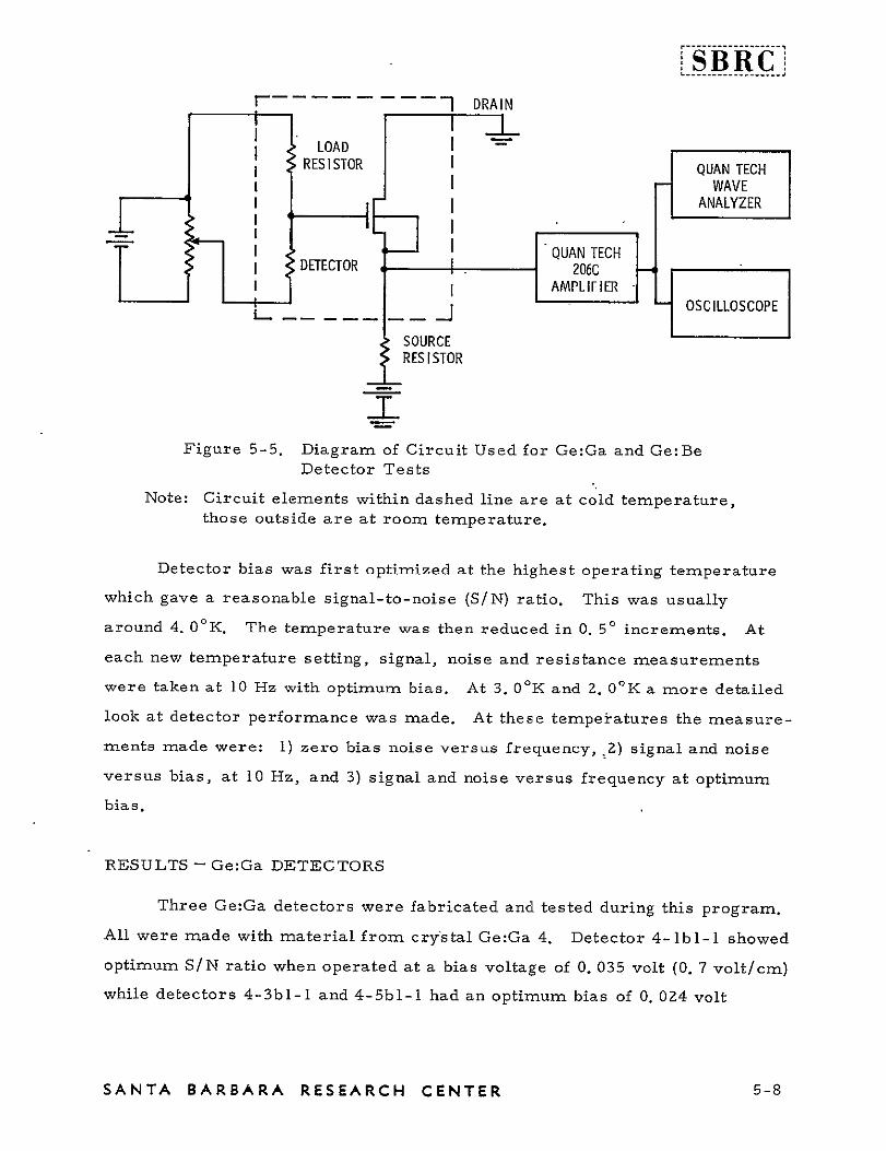
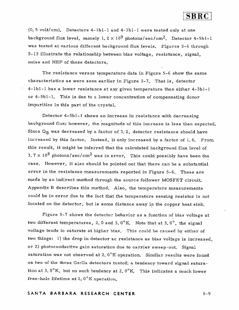
SBRC
(0 5 voltcm) Detectors 4-lbl-l and 4-361-1 were tested only at one
background flux level namely 1 Z X 10 9 photonsseccm Z Detector 4-5bl-l
was tested at various different background flux levels Figures 5-6 through
5-13 illustrate the relationship between bias voltage resistance signal
noise and NEP of these detectors
The resistance versus temperature data in Figure 5-6 show the same
characteristics as were seen earlier in Figure 3-7 That is detector
4-lbl-l has a lower resistance at any given temperature than either 4-3b1-i
or 4-5bl-i This is due to a lower concentration of compensating donor
impurities in this part of the crystal
Detector 4-5b1-l shows an increase in resistance with decreasing
background flux however the magnitude of this increase is less than expected
Since QB was decreased by a factor of 3 2 detector resistance should have
increased by this factor Instead it only increased by a factor of 1 6 From
this result it might be inferred that the calculated background flux level of
3 7 X 10 8 photonsseccm 2 was in error This could possibly have been the
case However it also should be pointed out that there can be a substantial
error in the resistance measurements reported in Figure 5-6 These are
made by an indirect method through the source follower MOSFET circuit
Appendix B describes this method Also the temperature measurements
could be in error due to the fact that the temperature sensing resistor is not
located on the detector but is some distance away in the copper heat sink
Figure 5-7 shows the detector behavior as a function of bias voltage at
two different temperatures Z 0 and 3 00 K Note that at 3 00 the signal
voltage tends to saturate at higher bias This could be caused by either of
two things 1) the drop in detector ac resistance as bias voltage is increased
or 2) photoconductive gain saturation due to carrier sweep-out Signal
saturation was not observed at 2 00 K operation Similar results were found
on two of the three GeGa detectors tested a tendency toward signal saturashy
tion at 3 0degK but no such tendency at 2 0degK This indicates a much lower
free-hole lifetime at 2 00 K operation
SANTA BARBARA RESEARCH CENTER 5-9
------------
a - p
ol
4-3b-I Q bull 12 x109phsC 2m-2
l4-Tbl-L Q8 - 12x 109 ph sc Cmn2
24-5b1-L Q8 37 x108phsec-I cm 9 1144b11 Oi3 seIDSb-O~-12xI I phsC mm
20 25 30 35 40 45 DETECTOR IMTEMPERATURE
Figure 5-6 Resistance Versus Temperature for GeGa Detectors
SIGNAL 1O-
4 loll
010--5- 10
2 A RESISTANCE -~
E
I~NOISE
10-6-0 9
ORIGINAL PAGE IS
NIPN0 OF POOR QALITY
~2degK 3degK
001 00 a 0 D4o 0w 04060 awo DETECTOR tolts)VOLTAGE
Figure 5-7 Signal Noise NEP and DC Resistance Versus Bias Voltage for GeGa Detector No 4-lbl-l at Two Temperatures (10 Hz Data)
SANTA BARBARA RESEARCH CENTER 5-10
The detector resistance decreases with increased bias This is due
primarily to an increase in free carrier density because of an increasing
lifetime with bias
The noise voltage at low bias is predominantly preamplifier noise As
bias voltage is increased detector noise becomes evident
The NEP is higher at low bias voltage because of the preamplifier
contribution to the noise At higher bias it tends to level off This is
typical of most GeGa detectors that have been tested Some however
have shown a clear minimum and then an increasing NEP at higher bias
probably due to an excess detector noise arising at the detector contacts
The detector signal data in Figures 5-8 and 5-9 can be used to calculate
detector responsivity values and from these one can obtain estimates of
quantum efficiency and photoconductive gain The voltage responsivity at
wavelength X is a function of frequency due to the circuit RC rolloff This
frequency dependence can be written as I
Rv(Xf) = Rv(X o) [1 + (ZlfTRRc)Z] - 2 (7)
where Rv(X o) is the dc or low-frequency responsivity and TRC is the circuit
response time By fitting a curve having the functional dependence on
frequency shown by this equation to the signal data in Figures 5-8 and 5-9
it was found that the 1-Hz responsivity values are sufficiently close to the
dc value to be used in an approximate calculation The 1-Hz voltage responshy
sivity was calculated from experimentally measured data using the formula
RVXI)- S (AX) (8)Rv(X 1) = HBB(AnX)ADg
where S(AX) = signal voltage measured at output of preamplifier
HBB(AX) = blackbody irradiance at detector (see Table 5-1) 3
AD = detector area (7 5 X 10 - cm 2 )
g = preamplifier gain (0 85)
SANTA BARBARA RESEARCH CENTER 5-11
4-lbl- 4-3b1-1 4-5b1-l
10-3
- SIGNAL
04
10-5
-6
NOISE
PREAMPLIFIER
8 l10 - i i i l
1 10 100 1000
FREQUENCY (Hz) Figure 5-8 Signal and Noise Versus Frequency for GeGa
Detectors at 3 00 K
Note Background photon flux density was 1 2 X 10⁹ ph sec - I cm - Z
Signal and noise values are referred to the output of the MOSFET preamplifier
SANTA BARBARA RESEARCH CENTER 5-1Z
SBRCI ----- 1--T-T- -r---------TT--------T-shy
10 _
o 10-5
SIGNAL
0 2
10- 7 PREAMPLIFIER
NOISE
4-1bl-1 QB = 12 x 109 ph sec - I cm -shy 4-3b1-1 QB = 12 x 109 ph se-C mshy2
4-5b1-1 QB = 12 x 109 ph sec - I cm- 2
10_8 4-5b1-1 QB = 37 x 108 ph sec - 1 cm shy 2
1 10 100 1000 FREQUENCY (Hz)
Figure 5-9 Signal and Noise Versus Frequency for GeGa Detectors at Z 00 K
Note Background photon flux density was 1 Z X 10 9 ph sec-I cm-Z Signal and noise values are referred to the output of the MOSFET preamplifier
SANTA BARBARA RESEARCH CENTER 5-13
-SB -RC
The short-circuit current responsivity was calculated from the voltage
responsivity using the equation
is(X 1) = Rv(X 1)R (9)11
where R11 is the parallel resistance formed by the load and the detector ac
resistance values
RacRLH11 = Rac + RL (10)
and
[ V dRdc-Rac = Rdc l - - (11)I Rdc dV
According to detector theory the short-circuit current responsivity is given
by
w e= c GP c (lZ)
Lc = photoconductive gain
7 = free-hole lifetime
S= hole mobility
E = electric field strength
L = interelectrode spacing
77 = quantum efficiency
e = electronic charge
X = wavelength
h = Plancks constant
c = speed of light
Therefore once a value for I(X o) is obtained some estimates of values for
17 and Gpc can be made
Using the foregoing equations and the measured experimental data
values of current responsivity were calculated for the three GeGa detectors
The results for operating temperatures of both 2 0 K and 3 00 K are shown
in Table 5-Z The current responsivity values are at the peak of the detectors
SANTA BARBARA RESEARCH CENTER 5-14
i-SBRCj]
Table 5-Z Parameters Used in Calculation of Short-Circuit
Current Responsivity for GeGa Detectors
DETECTOR NUMBER TEMPERATURE PARAMETER UNITS 4 (OK)
4-]b1-1 4-3b1-1 4-5b1-1
BIAS VOLTAGE VOLTS 0035 0024 0024 20 AND 30 ELECTRIC FIELD VOLTSICM 070 048 048 20 AND 30
10 x I010 Rdc OHMS 5 K 109 14 x 10I0 30
Rac OHMS 28x 109 73 x 109 Li x 1010 30
S(AX 1) MILLIVOLTS 044 020 019 30
RV(Ap 1) VOLTSIWATT 86 x i010 39 X 1010 37 x 1010 30
Is(p 1) AMPS WATT 32 (10) 61 41 30
nGpc (0124) 0076 0051 30
Rdc OHMS 16 x 1010 20 x 1010 31 x 1010 20
Rac OHMS 12 x 1010 13 X 1010 24 x 1010 20
S(441) MILLIVOLTS 023 012 015 20
x 1010 Rv(Xpl) VOLTSWATr 4 5 X 10¹⁰ 23 29 x 1010 20
Is(Ap 1) AMPSWAnT 46 22 18 20
flGpc 0057 0021 0022 20
RL - 5 x 10¹⁰ (NOMINAL VALUE)
Xp = 100 Pm 0hAT VAGE IS
AD - 7 5 x 10⁻³ cm2 (15 x 05 mm) ORUGNL- ALI OF pOOR Q
f =IHz
pm An exceptionallyspectral response curve which was taken to be 100
0 high value of current responsivity was obtained for detector 4-lbl-l at 3 O K
No obvious experimental error could be found in the data however the result
does seem to be spurious By comparison of the Z 00 and 3 00 K current
value around 10responsivities of the other two detectors it appears that a
ampswatt would be more appropriate for this detector The current
responsivity for this detector would be expected to be somewhat higher than
the others because of a higher applied bias and longer free carrier lifetime
Both ofthese conditions lead to a higher photoconductive gain for this detector
The signal versus bias voltage data shown previously in Figure 5-7 indicate
that the photoconductive gain could be on the order of 0 5 (This result is
of course based on the assumption that the maximum value of the gain at
saturation is 0 5 ) The use of these results in Equation (12) leads to a
5-15SANTA -BARBARA RESEARCH CENTER
quantum efficiency of 0 Z5 which seems reasonable considering the Ga doping
concentration used in these detectors The other two detectors probably are
operating with a photoconductive gain around 0 Z at 3 O0 K For Z 00 K
operation a decrease in current responsivity by a factor about 2 5 is
observed This must be attributed to a decreased photoconductive gain of
the same amount since the quantum efficiency would not be expected to
change simply because of a change in operating temperature
The measured signal-and-noise data was used to calculate the NEP
data which is shown in Figures 5-10 5-11 and 5-1Z The NEP versus
frequency data shows an essentially flat behavior from 1 to 40 Hz and then
rises slowly An effort was made to measure detector noise data at frequencies
below 1 Hz using a spectrum analyzer The data obtained were unreliable
thus not reported here
The NE versus temperature data of Figure 5-12 show a fairly clear
minimum at 3 00 K operation At higher temperatures NEP increases due to
increasing detector generation-recombination noise and decreasing detector
resistance At lower temperatures the NEPincrease is mainly due to a
decreased detector responsivity The conclusion is that the optimum operatshy
ing temperature is close to 3 00OK NEP values of about 0 7 to 1 X 10-16 1
wattsHz2 were achieved with a background flux of 1 2 X 10⁹ photonsseccm Z
One detector number GeGa 4-5b-i was also measured at various
different background flux levels Figure 5-13 shows a plot of calculated NEP
values versus frequency at four different flux levels At the highest backshy
ground flux NEP rises in the low-frequency range This is due to 1f noise
in the detector At the lower background flux levels NEP shows less
dependence on frequency and is reasonably flat down to 1 Hz - The lowest1
-measured NEP was 4 X 10 - 1 7 wattsHz at I -lz with a background level of
3 7 x 10 8 photonsseccm z
SANTA BARBARA RESEARCH CENTER 5-16
10-15 iI iF ---- I~t T--
T4-lbl-1 QB 12 x 109-E s---f1j2 -I -2
4-3b1-1 QB = 12 x 109 ph sec cm 1 -2
4-5b1-1 QB = L2 x 109 ph sec- cm
QB -37 x 108 ph sec- cm -2 4-5b1-I
1 1 4 - - --- o
1 0 -17 [ 1 1 1 1 1 I1 1 1 II I
1I0 100 1000
FREQUENCY (Hz)
Figure 5-10 NEF Versus Frequency for GeGa Detectors at 3 OdegK
10-1
I -2 4-Ibi-1 QB - 12 x 109 ph sec cm
I -2 4-3bl-1 QB = 12 x 109 ph sec cm
I 24-5bl-1 Q8 12 x 109 ph sec Cm
- 2 4-56l1-I 37 x 108 phsec 1 cmQB shy
__ 1
iiiI fl LLII I it
1 10 100 1000
FREQUENCY (Hz)
Figure 5-11 NEP Versus Frequency for GeGa Detectors at Z00 K
SANTA BARBARA RESEARCH CENTER 5-17
iSBRC]
4-1E- OB 1]2 x ]09 ph sle c 2
4-31-L Q8 L2 X109ph se-t cm-2 4-b1-1 QB - 12 x 109 phse 1 cm 2
4-5b1-L QBshy3 7 X10⁸ ph seC1 cm -2
t
I IT
-----I
1WI71
20 25 30 3r5 4 0 4 5
TEMPERATURE(K1
Figure 5-1Z NEP Versus Temperature for GeGa Detectors at a Frequency of 10 Hz
SQB- 124 x 109 phseccm2
QR 3 7 x 10⁸ phlseclcm2
Q8 = 175 x 1010 phlseccm 2
BQ 117 x j112 phseclcm2
10_14 _________ ________ _______
- NOTE SCALE CHANGE
S --shy _-shy
1 10 100 1000
FREQUENCY (Hz)
Figure 5-13 NEP Versus Frequency for GeGa Detector 4-5b-I at 3 00 K for Four Different
Background Flux Levels
SANTA BARBARA RESEARCH CENTER 5-18
r ---------------SBRC
RESULTS - GeBe DETECTORS
As mentioned previously all three GeBe detectors fabricated and
tested on this program were cut from the same slice of crystal Ge Be 10
The slice number was 3a and the location of this slice in the crystal was
adjacent to slice 3 from which the Hall sample was taken The Be doping
1 3 X 10 1 5 concentration was atomscm 3 Figures 5-14 through 5-Z0
illustrate the relationship between bias voltage resistance signal noise
and NEP of these detectors lt
In Figure 5-14 the signal is seen to be a linear function of bias voltage
and does not tend to saturate as did the GeGa detectors The resistance is
seen to be nearly constant with bias voltage to it can be assumed that Rac
is equal to Rdc The NEP is higher at low bias due to preamplifier noise
and then decreases tending to flatten out as bias increases This is quite
evident at Z 00 K operation but for this particular detector at 3 00 K the
NEP starts rising prematurely due to excess detector noise The other
detectors tested showed the flatter NEP curve at both operating temperatures
Figure 5-15 shows the measured resistance versus temperature data
The detectors all have similar resistance values as would be expected for
detectors cut from the same slice of material Since this material did not
show significant hopping conductivity the resistance is background photon
limited at the lowest temperatures with a value of Z 5 X 10 1 0 ohms This
resistance value is substantially lower than might be expected based on a
theoretical calculation The background limited dc resistance can be
expressed as
Rdc - L cflQBTepiw
(13)
ORIGINAL PAGE IS OF POOR QUALITY
SANTA BARBARA RESEARCH CENTER 5-19
--- S- --- -shy
- ~ SIGIAL
---20K
i0 5 IOU
6I0- -1-
NOISE RESISTANCE
Detector Voltage for CeBe l0-3a-3 at TwoTemperatues 2degK and 3K
-10-33-1 10-3a-2
010-ashy
109
20 2 303540 45s DETECTOR (KT5MPERATURE
Figure 5-15 Resistance Versus Detector Temperature of Ge Be Detectors
Note Background photon flux density was 0 9 X 10 9 ph sec-1 cm-2
SANTA BARBARA RESEARCH CENTER 5-Z0
LSBRC
Inserting the following values into this equation
- ZL = 5 X 10 cm
T7 =03
QB = 9 X 10⁸ photonsseccm Z
i =10 - 7 sec
e = 16 Xl0- 1 9 coul
ii = 4 X 10⁵ crZvolt sec
w = 1 5 y0-1 cm
gives a value for Rdc of 1 9 X i01 ohms nearly an order of magnitude
higher than measured All the above parameters except 71 QB and T came
from direct measurements The 77and T values are reasonable approximations
which should be within a factor of 2 or 3 of the true values It would be
necessary to increase the 77 product by a factor of 10 to bring the calculated
Rdc into agreement with the measured value This seems to be unreasonable
therefore it must be concluded that QB is actually higher than the stated
value of 9 X 10⁸ photonsseccm z
Figures 5-16 and 5-17 show measured signal-and-noise data versus
frequency for two operating temperatures The signal data can be analyzed
in the same way as for the GeGa detectors to obtain short-circuit current
responsivity values and estimates of the 1]Gpc product The results are given
in Table 5-3 The blackbody signal radiation was restricted to the 16- to
22-gim band by a filter Therefore direct use of Equation (8) gives the
voltage responsivity at a wavelength of -about 19 pLm To convert this value
to responsivity at the peak of the GeBe spectral response which is at 40 pLm
the calculated responsivity was multiplied by a factor of 2 This factor is
based on the relative spectral response of GeBe reported by Shenker et al 12
All the values of voltage and current responsivity listed in Table 5-3 are at
the detectors peak wavelength of 40 pLm The calculated current responsivity
values are seen to be in the neighborhood of 2-5 ampwatt DetectorGeBe 10-3a-3
1Z See Reference 5
SANTA BARBARA RESEARCH CENTER 5-21
tllm I - r rt irn I ITII41
10-3a-1 10-3a-2 10-3a-3
10-3 N
SIGNAL
10shy4
J4______
-
C
10-5
CNOISE
PREAMPLIFIER NOISE 10-7 shy
-RIGINAL PAGE IS OF POOR QUALTY
1 10 100 1000 FREQUENCY (Hz)
Figure 5-16 Signal and Noise Versus Frequency for GeBe Detectors at 3 00 K
Note Background photon flux density was 0 9 X 1-09 ph sec- 1 cm-Z Signal and noise values are referred to the output of -the MOSFET preamplifier
5-ZZSANTA BARBARA RESEARCH CENTER
l II IIIII~~~SR
-L1B3ashy
10-3a-1 - ------10-3a-2 --- 10-3a-3
10- 41______ __
10-4
a V SIGNAL
-shy4
PREAMPLIF IERNOS
- 810 1 a I l i l t I J l
1I0 100 1000
FREQUENCY (Hz)
Figure 5-17 Signal and Noise Versus Frequency for GeBe Detectors at 2 OdegK
Note Background photon flux density was 0 9 X 10 9 ph sec-i crn-Z
Signal and noise values are referred to the output of the
MOSFET preamplifier
SANTA BARBARA RESEARCH CENTER 5-23
SBRC L -
Table 5-3 Parameters Used-in Calculation of Short-Circuit Current Responsivity for GeBe Detectors
UN ITS DETECTOR NUMBER TEMPERATUREPARAMETER 10-3a-3 (OK)10-3a-1 1O-3n-2
BIAS VOLTAGE VOLTS 0235 0235 0082 30 ELECTRIC FIELD VOLTSICM 470 470 164 30
Rac OHMS 19 x 1010 22 x 1010 18 x 1010 30 S(AX 1) MILLIVOLTS 18 19 056 30
Rv(Xp 1) VOLTS(WAT 66 x 1010 69 x 1010 20 x 1010 30
Is(Xp 1) AMPSWAIT 57 54 18 30
flGpc 0176 0167 0056 30
BIAS VOLTAGE VOLTS 0259 0353 0188 20
ELECTRIC FIELD VOLTSICM 519 705 376 20
Rac OHMS 22 x 1010 26 x 1010 27 x 1010 20
S(AX 1) MILLIVOLTS 15 11 11 20
Rv(Ar 1) VOLTSIWAIT 55 x 1010 40 x1010 40 x 1010 20
Is(Xp 1) AMPSIWATT 43 29 28 20
1GPC 0133 0090 0081 20
RL =3 x 10¹⁰ OHMS (NOMINAL VALUE)
Ap = 40 pm AD 75 x 10-3 cm2 15 x 05 mm)
I =1 Hz
was somewhat lower than the other two because it had to be operated at a
lower bias voltage If one assumes a quantum efficiency of 0 3 then the
photoconductive gains would be in the range of 0 2 to 0 6 These are
reasonably values for the low-frequency gain (I Hz) which would not be
limited by carrier sweep-out
Calculated NEP values are plotted versus frequency and temperature
in Figures 5-18 5-19 and 5-20 Figures 5-18 and 5-19 show the NEP to be
essentially flat with frequency between I and 10 Hz and then rising for higher
frequencies An exception is Detector GeBe 10-3a-Z which appears to have
some excess noise in the I- to 2-Hz range causing an increased NEP at these
low frequencies
5-24SANTA BARBARA RESEARCH CENTER
ISBRCI
-10-14
10-3a-I 10-3a-2 -
S 10-3a-3shy
-15 10 shy
IO-16 l
1 10 100 1000 FREQUENCY (Hz)
Figure 5-1-8 NEP Versus Frequency for GeBe Detectors at 3 00 K
- I - Z Note Background photon flux density was 9 X 10⁸ ph sec cm
10-14 j1n --- 1 i-- r- r r rr
1O-3a-1 110-3a-2
- -- 10-3a-3
0-1
1o-16 ORIGINAL PAGE IS OF POOR QUALITY
- 1 7 10 1 1 1 1 I Ii t - 1 -1 1 t 1I I l
1 10 100 100
FREQUENCY (Hz)
Figure 5-19 NEP Versus Frequency for GeBe Detectors at 2 00 K
- -z Note Background photon flux density was 9 X 10⁸ ph sec I cm
SANTA BARBARA RESEARCH CENTER 5-Z5
SBRCI
The NEP versus temperature data in Figure 5-Z0 showa reasonably
flat behavior between Z 0 and 3 00 K and then rise at higher temperature
An exception here is detector GeBe l0-3a-3 which reaches its lowest NEP
only at Z 00 K This ditector had to be operated at a lower bias voltage than
the others because it became excessively noisey at higher bias This
problem was most likely due to contact noise The minimum NEP is about
the same for all three detectors and is Z to 3 X10⁻¹ 6 wattsHz2
10-3a-I 10-3a-2 10-3a-3
15 10shy
=
-10 16 1 I 1 3 1 I 20 25 30 35 40 45
DETECTOR TEMPERATURE (OK)
Figure5-ZO NEP Versus Detector Temperature for GeBe Detectors
Note Background photon flux density was 9 X 10 8 ph sec-1 cm-Z
SANTA BARBARA RESEARCH CENTER 5-26
Section 6
CONCLUSIONS AND RECOMMENDATIONS FOR FUTURE WORK
This work has provided significant advancements in the technology of
GeGa and GeBe photoconductive detectors for use in astronomical observashy
tions at wavelengths from 30- to 1Z0-gm All the major goals for this phase
of the development were accomplished The primary conclusions that can
be drawn from the work performed thus far are as follows
GeGa DETECTORS
A Ge purification method was developed which reduces the residual
donor impurity concentration to the 1010 atomscm 3 range Residual
acceptor impurity content may be much higher but is inconsequential
to detector performance
shown to produce Introduction of Ga by the zone leveling method was
uniformly doped ingot with sufficient material for fabrication ofa many detectors The doping concentration can be controlled within
an acceptable tolerance
Crystals doped to Z 5 X 10¹⁴ Ga atomscm 3 do not show hopping
conductivity Higher doping concentrations might be useful for
increasing the detectors quantum efficiency
Short-circuit current responsivity for 100 gm radiation was measured
to be in the range of 6 to 10 ampswatt at 3 0 0 K operation This
implies an 77Gpc product of 0 074 - 0 IZ4 Quantum efficiency was
estimated to be around 0 25
Detectors were not enclosed in an integrating cavity The use of
such a scheme 1could significantly improve quantum efficiency
An NEP of 4 X 10-17 wattsHz2 was measured at 1 Hz with a backshy
ground flux of 3 7 X 10⁸ photonsseccm Z at 3 00K operating
temperature This comparesfavorably with the calculated BLIP
value of 1 X10-17 wattsHz2 (77 =-0 30 Xp = 100 gm)
The NEP is minimized at an operating temperature very close to
3 0degK Higher or lower operating ter-peratures may cause a
degradation of NEP
Reproducibility and yield of good detector elements were excellent for
GeGa detectors Most of the technology development on this material
has been completed and the producibility of detectors which meet or
exceed the NEP objectives for the IRAS mission has been demonstrated
SANTA BARBARA RESEARCH CENTER 6-1
SBRC
GeBe DETECTORS
Oxygen must be eliminated during growth of GeBe crystals to prevent Be-O complexing A vacuum zone melting process was developed which provided a method for doing this
10 1 5 The Be concentration should be kept below Z X atomscm 3 to prevent impurity hopping conductivity from seriously lowering detector resistance at 3 00 K
The electric field strength that can be applied to uncompensated GeBe is limited to less than 10vcm due to impact ionization of shallow acceptor levels
o Short-circuit current responsivity for 40 pLm radiation was measured
to be in the range of Z to 5 ampswatt for 3 00 K operation
Detectors were not enclosed in an integrating cavity The use of such a scheme could significantly improve quantum efficiency
- 1 6 O The lowest measured NEP for GeBe detectors was 2 to 3 X 10
wattsHz I
at a frequency of I Hz with a background flux of 9 X 10⁸
photonsseccm 2 The BLIP value for this background is 4 6 x( i017 wattsHzi (7 = 0 3 Xp = 40 ptm)
The NEP is optimized at 3 00 K or lower There was no clear indication of a minimum in the NEP versus temperature plot
The yield of GeBe detectors from a given slice of material was acceptable Two out of three detectors fabricated and tested had reasonably good performance the third had excessive 1f noise
The uniformity of GeBe material properties within a slice is excellent Uniformity over a whole ingot has not yet been achieved
The producibility of GeBe detector elements is presently limited by the crystal material uniformity and quality
RECOMMENDATIONS FOR FUTURE WORK
In the case of GeGa recommendations for future work could be called
minor technological improvements The work accomplished to date has
shown that GeGa detectors can meet the objectives of the IRAS mission
However minor improvements might still be achieved For example
GeGa crystals with a Ga concentration greater than Z 5 X 10¹⁴ atomscm 3
should be grown and evaluated to see if the quantum efficiency can be
improved Also the use of integrating cavities for improvement of quantum
efficiency should be investigated
SANTA BARBARA RESEARCH CENTER 6-2
Measurements of detector behavior at frequencies below I Hz should
be made Although data taken to date show no evidence of any problem in
this frequency range confirming measurements should be made
In the case of GeBe the crystal growth technology needs further
improvement It is recommended that more work be done in two areas
First the method of zone leveling to produce a uniform Be concentration
along the whole ingot should be implemented With the existing method
variation of Be concentration along an ingot is still too great to give a
sufficient quantity of material for focal plane array production Secondly
crystals of compensated material should be grown and evaluated to see if they
have any advantage over the uncompensated material which has been used
in past work The uncompensated material must be operated at low electric
field strengths to prevent impact ionization of the shallow acceptors In
compensated material electric field strengths 4 to 5 times larger should
be permissible This could give an improvement in photoconductive gain
provided that the hole lifetime is not seriously degraded by the additional
compensating donors Careful control will be needed to avoid introduction
of too manV compensating donors
As mentioned for the case of GeGa detectors the use of integrating
cavities should also be investigated for GeBe detectors Finally measureshy
ments of detector behavior at frequencies below I Hz should also be made
SANTA BARBARA RESEARCH CENTER 6-3
-SBRC-
Appendix A
IRRADIANCE CALCULATIONS
This appendixpresents details of the calculation of blackbody signal
irradiance and background photon flux density at the detector focal plane in
the low-background test dewars
GeGa TEST DEWAR
As mentioned in Section 5 in the main text the GeGa detectors were
tested using a long-wavelength pass filter consisting of two pieces of special
black polyethylene and crystal quartz These materials along with the
detectors natural cutoff at about 120 pLm produced a relative spectral response
as shown in Figure A-1 This isolated a spectral band about 35 pLm wide
in the 100-pim region Neutral density filters were also used to further
attenuate the background photon flux on the detector
The effective blackbody signal irradiance on the detector was calculated
by numerically integrating the blackbody flux over the filter spectral range
To do this the spectral range was broken up into intervals each 5 pLm wide
as shown in Figure A-1 The blackbody radiant emittance for each spectral
interval was then obtained from a radiation slide rule These values are
shown in Table A-1 along with the spectral intervals and the relative filter
transmittance in each spectral interval Since the signal radiation is
produced by the difference between the 500K blackbody and a 300 0 K chopper
blade these values were obtained from the slide rule and one was subtracted
from the other to obtain the actual signal radiant emittance in each interval
The difference values are listed in column 5 of the table Multiplication of
each number in column 5 by the corresponding -relative filter transmittance
SBRC is indebted to K Shivanandan of NRL for furnishing these data
SANTA BARBARA RESEARCH CENTER A-1
10
09
r
I
-n
L
08 r
07
L
06 I
Co
c4 05
LO
II I 04
03 I
r
-IL
I
I
II
02 SI I
01
I
0 50
I
60
Figure A-I
I
70 80 90 100 110 120 WAVELENGTH (pm)
Relative Spectral Response of GeGa Detector with Long Wavelength Pass Filter
I
i
130
SANTA BARBARA RESEARCH CENTER A-Z
V) Table A-i Listing by Spectral Interval of Blackbody Signal Radiant Emittance and gt Background Photon Flux Values Used for GeGa Detector Testing z -i
(1) (2) (3) (4) (5) (6) (7) (8) w (X)gt RF(X) W500(A) W300(X) W500(X) -W300(X) WBB(A) Q30O QB(X)
4m) (wcm2) (wlcm2) (wcm2) (wcm2) (phseccm2) (phseccm2)
x1O3 x1O-3 xlO- 3 xO-5 xl017 x 016
S40-45 0 1436 0670 0766 0 1430 P
m 45-50 0 0912 0444 0468 0 1060 0
r 50-55 0 070 0 632 0310 0322 2254 0818 057
gt 55-60 0125 0454 0230 0224 2800 0664 083
60-65 0165 0334 -0172 0162 2673 0540 089
65-70 0260 0248 0130 0118 3068 0441 115
m 70-75 0320 0190 0100 0090 2880 0364 117 z 75-80 0375 0150 0080 0070 2625 0312 117
0257 150 m
80-85 0585 0118 0062 0056 3276
85-90 0685 0094 0050 0044 3014 0220 151
90-95 0810 0076 0040 0036 2916 0186 151
00 95-100 0950 0058 0032 0026 2470 0157 149
00 100-105 0900 0050 0028 0022 1980 0144 130
0105-110 0750 0040 0020 0020 1500 0108 081
0102 061110-115 0600 0032 0018 0014 0840
115-120 0350 oo 0016 ~ WB(X 3o_910-4ooo 0030 ~ oooo0014 0490 0094 033
120-125 0100 0027 0014 0013 0130 0086 009 ~~~
QB( 300AX) =149 x 1017SUMMATION WBA)=32x0
ISBRC
in column Z gives the effective blackbody radiant emittance in each spectral
interval These values are listed in column 6 Summation overall spectral
intervals then gives the total blackbody radiant emittance in the filter pass band
This total radiant emittance number is then used in Equation (6) to
calculate the irradiance at the detector focal plane Also needed for this
calculation are the absolute peak transmittance values for each filter and
the dewar window These are as follows
Absolute Peak Transmittance
1 Quartz window 0 85 First neutral density filter 0 015 Second neutral density filter 0 06 Z Special black polyethylene filters (0 5Z) Z
Atmospheric water vapor 0 88
Total transmittance TR = 1 8 X 10- 4
A transmittance factor for atmospheric water vapor was also included
Although this produces a small effect on total transmittance it was found to
be not negligible The effect of atmospheric absorption was checked by
flushing the space between the blackbody opening and the dewar window with
dry nitrogen This produced an increase in a GeGa detectors signal by 13
Since it was impractical to continue flushing this space during all tests
the atmospheric correction factor was applied to the blackbody irradiance
calculation
The equation for signal irradiance Equation (6) in Section 5 was
written as WB(ZX)AB TR F
HBB(AX) = WBB(AX) BB (AI) SN DZ
A-4SANTA BARBARA RESEARCH CENTER
Substituting the values calculated above along with those other values listed
in Table 5-I gives
HBB(AX) _ (3 29 x 10-4)(7 85 X 10-3)(1 8 x 10⁻⁴)(0 4) - o xI - 13 wcm 2 (3 14) (8 59) Z
The background photon flux density at the detector plane was calculated
in a similar manner Column 7 of Table A-I lists 300 0 K photon flux density
values for each spectral interval as obtained from a radiation slide rule
Column 8 gives the effective values passing through the filter (column Z X 7)
and their sum over all the spectral intervals
Equation (5) in Section 5 was then used to calculate the background
photon flux density at the detector plane This equation is
QB(AX) = Q(300 0 K AX) TR sinz 82 (AZ)
The filter transmittance factor in this case does not include the outer
warm quartz window nor does it include the atmospheric water vapor loss
It includes just the two neutral density filters and the two special polyethylene
filters Thus TR = 2 4 X 10- 4 Using this value along with the appropriate
values from Tables A-I and 5-1 gives
BX) = (149 X 1017)(Z 4 X 10-48 59) = 1 Z X 109 phseccm z
CeBe TEST DEWAR
The GeBe Detectors were tested using a 16- to 2Z-vrn multilayer bandshy
pass filter plus neutral density filters on germanium The relative transshy
mittance curve for this band-pass filter is shown in Figure A-2 The blackshy
body signal irradiance through this filter was calculated by numerical
integration in the same manner as was described for the case of GeGa
Table A-Z lists the relevant data
sectRGIN AL
SANTA BARBARA RESEARCH CENTER A-5
09
08 I I I
II I IL I I I I
06-C
04 I I
03shy
02
01 I
15 16 17 18 19 20 21 22 23 24
WAVELENGTH (um)
Figure A-Z Relative Spectral Response with Band-Pass Filter
of GeBe Detector
A-6SANTA BARBARA RESEARCH CENTER OO 0 A-6uA yOF P00R
z -I wgt
gt
X
Table A-Z Listing by Spectral Interval of Blackbody Signal Radiant Emittance Background Photon Flux Values Used for GeBe Detector Testing
and
gt
m
(1)
X 10m)
(2)
RF(X)
(3)
W5go(X) (wlcm2)
(4)
W30j(X) (wlcm2 )
(5)
W500) - W30 ijX) (wcm2)
(6)
WBB(A) (wlcm2)
(7)
Q3 0(X) (phlseccm2)
(8)
QB(X) (phseccm2)
m gtx
0 -
m Z -1 m1
15-16 16-17
17-18 18-19
19-20
20-21
21-22
22-23
23-24
005 080
078 091
086
072
045
037
015
770 630
525 455
385
350
280
245
210
x I0-
220
175
152 138
129
110
097
087
074
x Io-3
550
455
373 317
256
240
183
158
136
x io-3
028
364
291 289
220
173
082
058
020
x i017
156
144
140 131
123
115
1-03
098
090
xI017
008
115
109 119
106
083
046
036
014
SUMMATION WBB(AX) 153 x 10-2 QB3 0QAX) 63 1017
0
4 lo
-SB-R--
Using the data from Tables A-Z and 5-I and substituting into Equation
(A l) gives
HBB(UX) = (1 53 X 1 0 -Z)(1 96 X 10-3)(1 0 X i0-4)(0 4) = 8 6 X 10 - I Z wcm Z (3 14) (6 65) Z
The background photon flux density at the detector was obtained by subshy
stituting data from Tables A-1 and 5-1 into Equation (AZ) to get
QB(300K A) = (6 36 x 1017)(1 0 X 10 -6 65) = 9 0 X 108 phseccm Z
DETECTOR RESPONSIVITY
The blackbody signal irradiance values calculated in this appendix were
used to obtain detector responsivity by the usual formula
V9(AX) (M) Rv(A) - HBB(AX) AD
where Rv(X) is the responsivity in voltswatt VS(AX) is the measured signal
voltage AD is the detector sensitive area and HBB(AX) is the effective signal
irradiance It turns out that this procedure yields the responsivity at the
peak of the filter spectral distribution Xp A derivation of this result is as
follows
If Rv(X) is the detector responsivity at any wavelength and Pgt is the
signal power per unit of wavelength (wattsnLm) on the detector at this waveshy
length then for a given wavelength range between X and XZ the detector
signal voltage will be given by Xz
Vs(AX) = f Rv(X) PX dX (A4) X 1
where AX refers to the spectral interval X1 - XZ
SANTA BARBARA RESEARCH CENTER A-8
L[SBRCJ
If the detectors Rv(X) curve is expressed as a relative response
normalized to unity as shown in Figures A-I and A-Z then equation (A4)
can be written as Xz
VS(AX) = Rv(Xp) f RR(X) PX dX (A5)
where RR(X) is the relative response ( 1 at Xp) and Rv(Xp) is the responsivity
at X p This equation can be rewritten as
Rv(Xp) = XV (A6)
j RR(X) PX d xl
The integral in the denominator is the same as HBB(AX) AD when
HBB(AX) is calculated by the numerical integration method described
previously in this Appendix Therefore the responsivity calculated from
equation (A3) is the responsivity at the peak of the relative spectral response
curve Xp
SANTA BARBARA RESEARCH CENTER A-9
Appendix B
DETECTOR RESISTANCE MEASUREMENTS THROUGH MOSFET
This appendix describes the method used for determining detector
resistance values when the detector is connected to the cryogenic MOSFET
source follower preamplifier
The circuit diagram is shown in Figure B- i The detector dc resistance
is given by
Rdc = VDI (B1)
where
I = VB(RL + Rdc) (BZ)
The voltage drop across the detector VD will appear at the MOSFET source
terminal multiplied by the gain of the source follower This voltage is
measured by observing the change in V S as the detector bias voltage is
switched from zero to ON Thus
V D = AVs0 85 (B3)
where LV S is the observed charge in source voltage and 0 85 is the source
follower gain Combining equations (BI) (BZ) and (B3) gives
Rdc RL ((B4)(085 yv) -1
Use of this equation requires prior knowledge of the load resistance
RL Since the load resistance value can vary with temperature and bias
voltage this may introduce considerable error into the determination of
Rdc by this method Values of VB and AVs can be measured with good
precision and will not produce a large error
SANTA BARBARA RESEARCH CENTER B-I
- ------------
VB I
LOAD I RESISTOR RL
DVs
DETECTOR I- Rdc I
L----- --
VB = BIAS VOLTAGE APPLIED EXTERNALLY ACROSS BOTH DETECTOR AND LOAD
= VOLTAGE DROP ACROSS DETECTORVD
VS = SOURCE VOLTAGE
Figure B-I Circuit Diagram for Low-Background Detector Testing
Table B-i shows measured resistance values versus temperature and
applied voltage for a typical load resistor used in the detector assemblies
delivered on this program It is clear from these data that good calibration
of the load resistor must be accomplished to obtain accurate values for
Rdc from equation (B4)
Table B-I Resistance Versus Temperature of Typical Load
Resistor Used in IRAS Device Assemblies
Resistance (Q) Resistance (Q) Resistance ()Temperature at at at
(K) OZO V 0zoo V Z00 V
I0 1 04 Z 3 8 X 10¹⁰ 3 7 x Z 7 X 10¹⁰
4 0 3 7 X 10¹⁰ 3 9 X 10¹⁰ 28 X 101 0
0 4 7 X 10 1 0 1 03 5 44 X10 1 3 2 X10
03 0 5 1 x I0 6 0 x I010 3 7 X 10 1 0
ORIGINAL PAGE 18 B-Z
SANTA BARBARA RESEARCH CENTER OF POOR QUALITY
Another obvious method for determining Rdc would be to attach an
additional wire to the detector at the connection to the MOSFET gate and
bring this lead out of the dewar Measurements of detector current and
voltage could then be made directly However tw6 problems arise with
this method First the additional lead to the detector produces an added
capacitance at the gate input which will cause the circuit response to roll
off at lower frequencies Since the combination of MOSFET gate input andshy
detector capacitance is only about 5 pf distributed capacitance from the
additional wire bould easily equal or exceed this value Secondly the
insulation resistance of the dewar feed-throughs has to be very high in fact
much higher than the detector resistance If detector resistance values are
in the 10 1 0 -ohm range the insulator resistance should be greater than i0 1 Z
ohms The metal-glass feed-throughs used on our dewars can have this
high an insulation resistance if properly cleaned and kept dry However
past experience has shown that they are easily contaminated with use and
leakage problems result It was because of these problems that the indirect
method of detector resistance measurement described above was adopted
SANTA BARBARA RESEARCH CENTER B-3
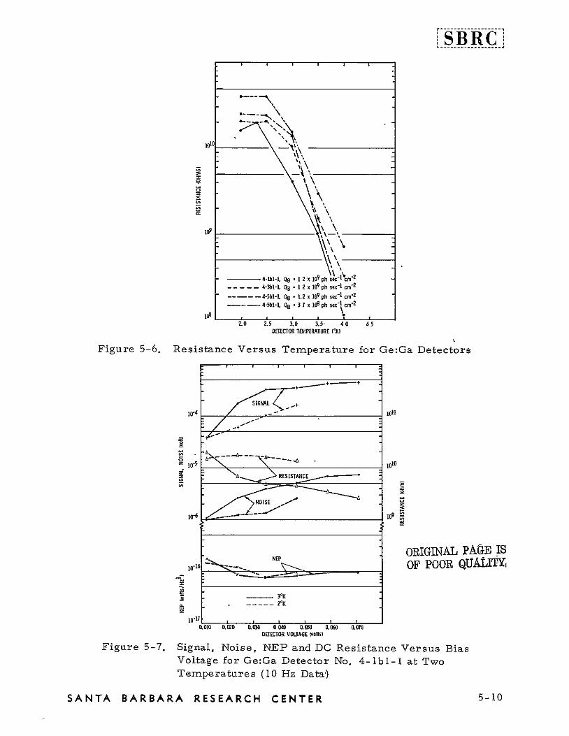
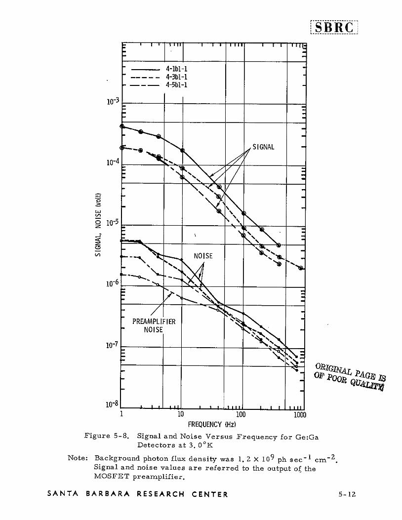
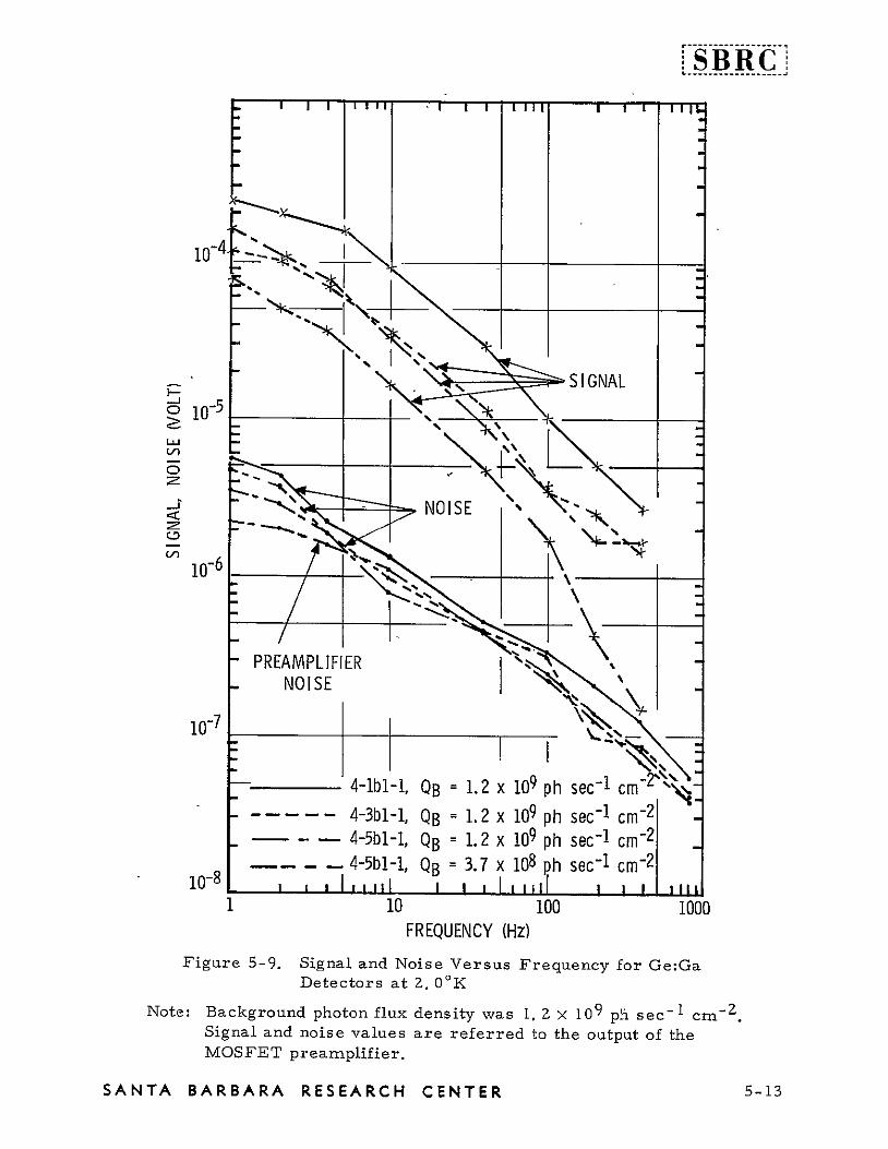
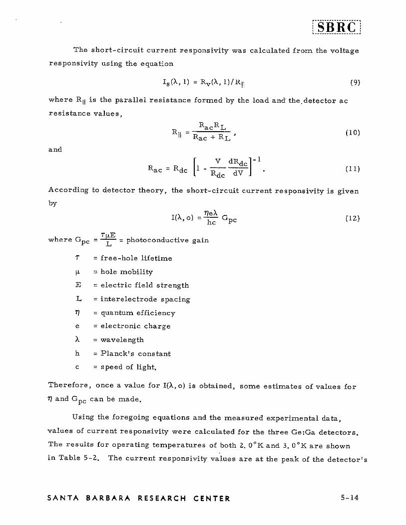
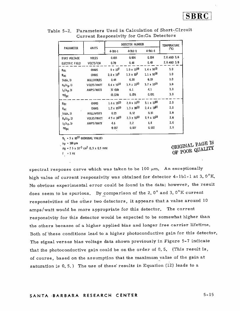
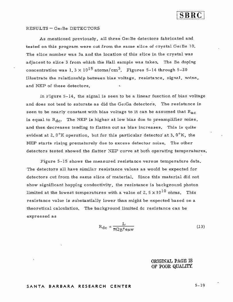
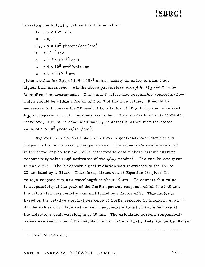
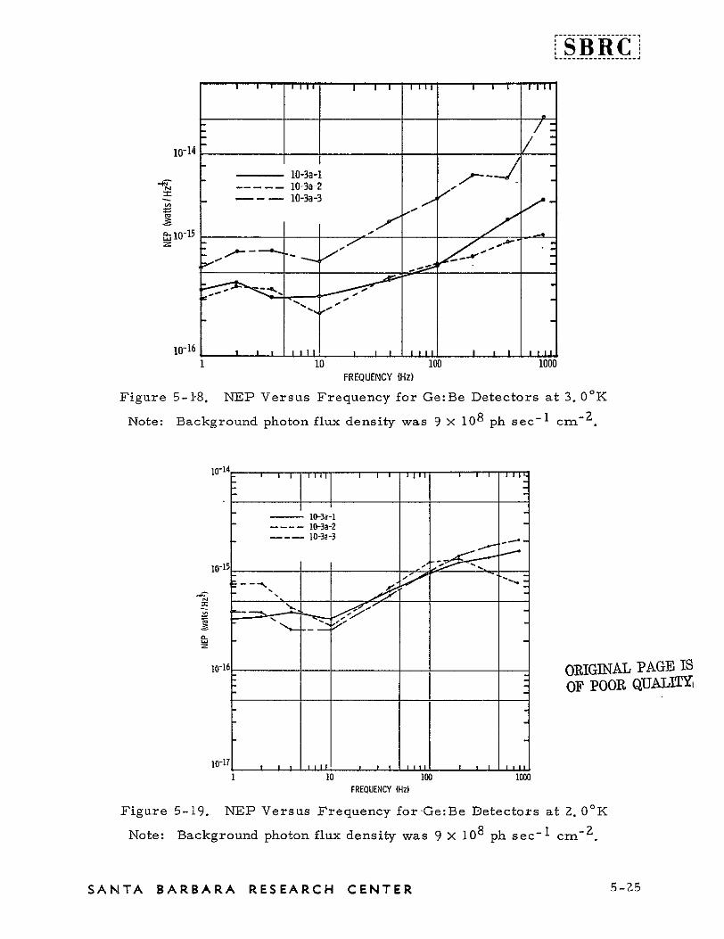
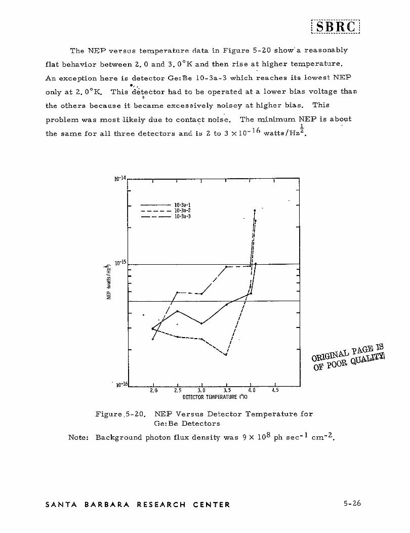
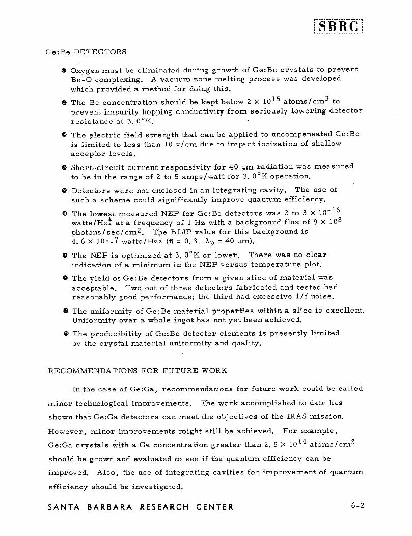
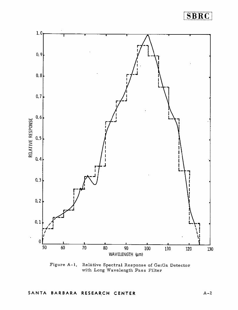
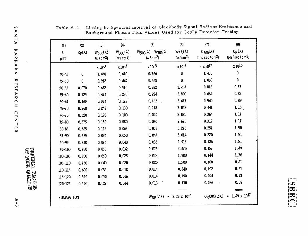
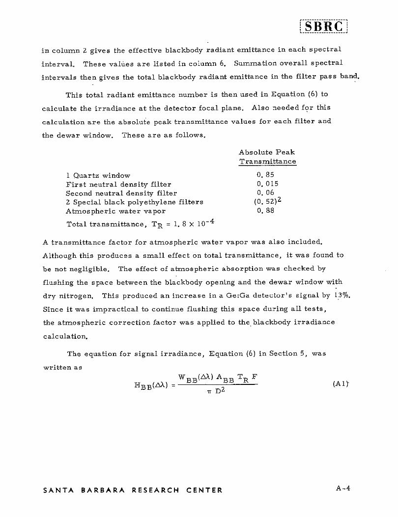
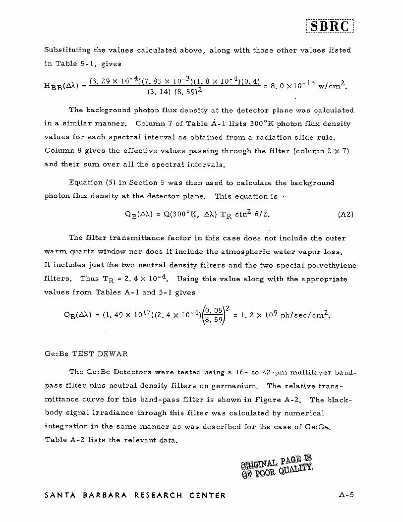
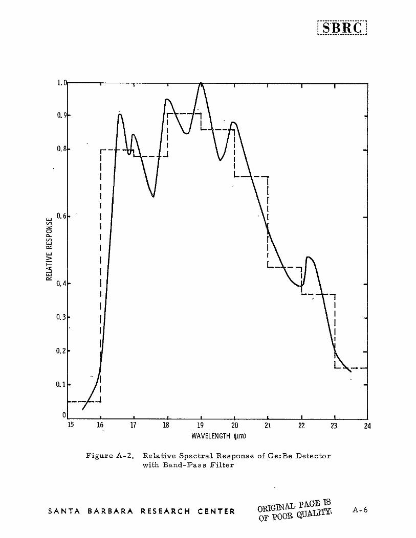
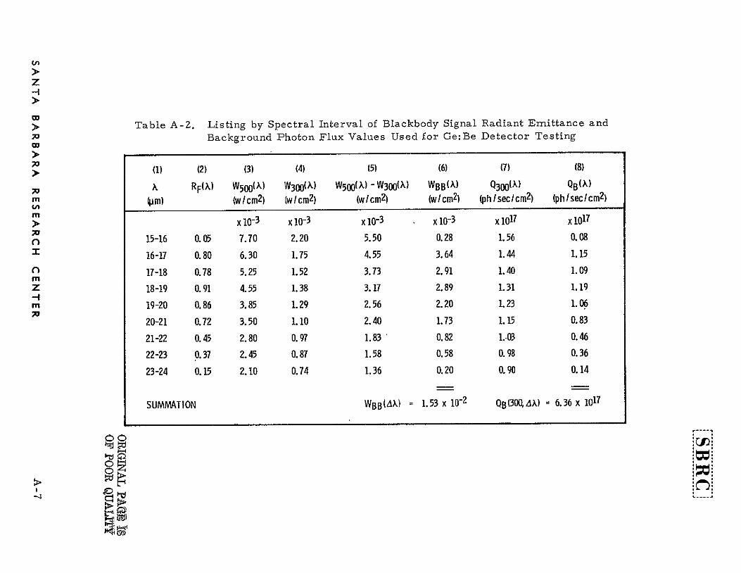
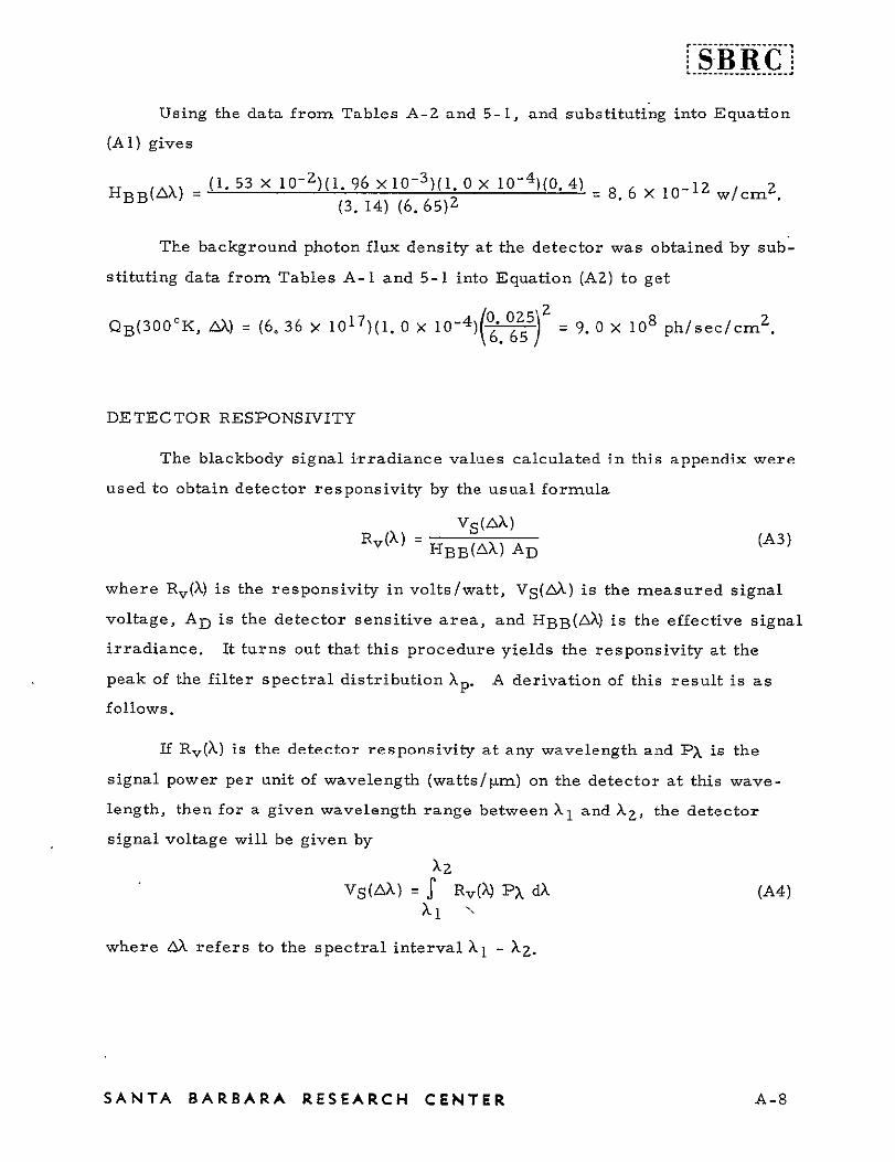
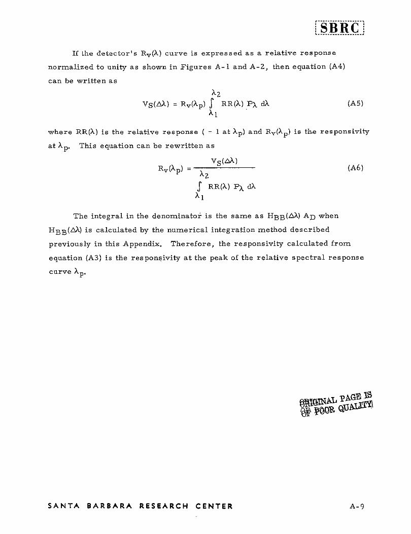
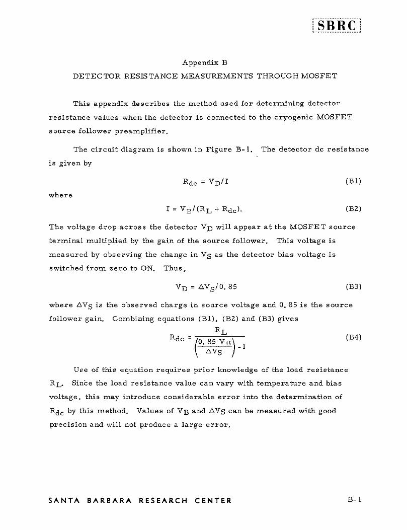
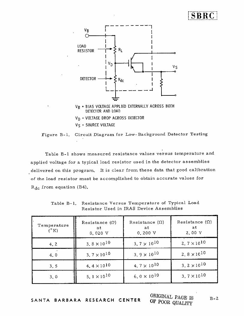