50Hz Colour Television DA100 and DW100 Chassis - slot techslot-tech.com/interesting_stuff/a...
23
50Hz Colour Television DA100 and DW100 Chassis
Transcript of 50Hz Colour Television DA100 and DW100 Chassis - slot techslot-tech.com/interesting_stuff/a...
50HzColour Television
DA100 and DW100Chassis
Colour Television – DA100/DW100 Chassis
Sharp Electronics (UK) LtdTechnical Support
September 99
Contents
POWER SUPPLIES...........................................................................................................................1
Switch Mode Power Supply......................................................................................................1Start up operation...........................................................................................................1Voltage regulation ..........................................................................................................2Over-voltage Protection..................................................................................................2Over-current control .......................................................................................................2
Slave Processor Power Supply.................................................................................................3Degauss Circuit........................................................................................................................45v Regulator ............................................................................................................................5
DA100 (59ESD7H and 66ESD7H) 4:3 chassis................................................................5DW100 (56FW53H to 6FW54H) 16:9 chassis .................................................................6
CLASS D OUTPUT STAGES ............................................................................................................7
Tda7480 Pin Functions.............................................................................................................7Pin 9 – Frequency ..........................................................................................................7Pin 12 – Mute/Standby function ......................................................................................7
Audio Output............................................................................................................................8Field Output .............................................................................................................................9
Vertical Fly-back...........................................................................................................10
VIDEO AND SYNC PROCESSOR...................................................................................................11
Description.............................................................................................................................11Analogue front-end.......................................................................................................11Input Selector...............................................................................................................11Clamping......................................................................................................................11Automatic Gain Control ................................................................................................12Analogue-to-Digital Converters.....................................................................................12Digitally Controlled Clock Oscillator ..............................................................................12Analogue Video Output ................................................................................................12Average Beam Current Limiting....................................................................................12Protection Circuitry .......................................................................................................12Scan Velocity Modulation Output ..................................................................................12
PICTURE ROTATION......................................................................................................................13
SCAN VELOCITY MODULATOR ....................................................................................................14
LINE OUTPUT STAGE....................................................................................................................15
East West Circuit....................................................................................................................16Circuit Description ........................................................................................................16
MICROPROCESSOR CONTROL....................................................................................................17
Reset .....................................................................................................................................18
PROTECTION .................................................................................................................................19
Microprocessor.......................................................................................................................19Audio Output ................................................................................................................19Beam Current...............................................................................................................19Horizontal Mute ............................................................................................................19
Video/Sync Processor ............................................................................................................20Safety ..........................................................................................................................20Vprot ............................................................................................................................20
Colour Television – DA100/DW100 Chassis
Sharp Electronics (UK) LtdTechnical Support
September 99 Page 1
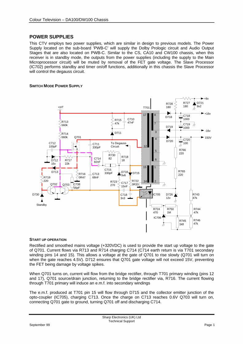
POWER SUPPLIESThis CTV employs two power supplies, which are similar in design to previous models. The PowerSupply located on the sub-board 'PWB-C' will supply the Dolby Prologic circuit and Audio OutputStages that are also located on PWB-C. Similar to the CS, CA10 and CW100 chassis, when thisreceiver is in standby mode, the outputs from the power supplies (including the supply to the MainMicroprocessor circuit) will be muted by removal of the FET gate voltage. The Slave Processor(IC702) performs standby and timer on/off functions, additionally in this chassis the Slave Processorwill control the degauss circuit.
SWITCH MODE POWER SUPPLY
START UP OPERATION
Rectified and smoothed mains voltage (+320VDC) is used to provide the start up voltage to the gateof Q701. Current flows via R713 and R714 charging C714 (C714 earth return is via T701 secondarywinding pins 14 and 15). This allows a voltage at the gate of Q701 to rise slowly (Q701 will turn onwhen the gate reaches 4.5V). D712 ensures that Q701 gate voltage will not exceed 15V, preventingthe FET being damage by voltage spikes.
When Q701 turns on, current will flow from the bridge rectifier, through T701 primary winding (pins 12and 17), Q701 source/drain junction, returning to the bridge rectifier via, R716. The current flowingthrough T701 primary will induce an e.m.f. into secondary windings
The e.m.f. produced at T701 pin 15 will flow through D715 and the collector emitter junction of theopto-coupler (IC705), charging C713. Once the charge on C713 reaches 0.6V Q703 will turn on,connecting Q701 gate to ground, turning Q701 off and discharging C714.
R713560k
R714560k Q701
C712100pF
Standby
D730
Q702 Q703
D713
R719220
R71722k
R7160R47
C71368nF
C711330pF
C71482nF
D711
C71047nF
T701
17
12
R73082
C715330pF D716
5v6D715
R7220R33
R723270
C71715nF
C7183n3
IC705
2
115
14
6
5
4D720 C720
100
150V
-16v3
7D719
C7191000
8D718 C718
1000
+16v
D71215v
+8v
D7218v2
R727180
R728180
R71547k
R71818
C73856pF
To DegaussCircuit
+HT
R766220
R765220
D72612v
R74347k
R74447k
R74647k
R724470
R7501M
IC706R7451k8
Colour Television – DA100/DW100 Chassis
Sharp Electronics (UK) LtdTechnical Support
September 99 Page 2
At this point, the magnetic field within T701 will collapse causing the e.m.f at pin 15 to go negativeturning Q703 off.
Q701 will not turn on until sufficient charge has built up on C714. However, at this time the negativeplate of C714 is approximately -12V; due to the collapsing field within T701. This results in the timeperiod required to build sufficient charge on C714 to bias Q701 on increasing i.e. Q701 off time = thetime for the back 'e.m.f.' to decade to zero, plus C714 charge time form zero to 4.5V approx.).
VOLTAGE REGULATION
The feed back through the opto-coupler (IC705), provides voltage regulation. The +150V line is usedas the controlling source and a reference is provided from the +16v supply.
Increase in load
As the +150V rail falls due to an increase in load (high beam current), the trigger voltage of IC706 willfall, increasing IC706 cathode voltage, reducing the current flowing through the LED section of IC705.This has the effect of decreasing the conduction of the photo transistor part of IC705. This increasesthe voltage drop across the collector/emitter junction; thereby increasing the time taken to chargeC713, delaying the point when Q703 turns on, turning Q701 off. Energy is transferred across T701 fora longer period, increasing the HT rail; hence, the frequency of the power supply will fall.
Decrease in load
As the +150V rail increase due to a decreasing load (low beam current), the trigger voltage of IC706will rise decreasing IC706 cathode voltage which increases the current flow through the LED sectionof IC705. This has the effect of increase the conduction of the phototransistor within IC705. Therebydecreasing the voltage drop across the collector/emitter junction; which will decrease C713 chargetime, advancing the point when Q703 turns off, turning off Q701 to turn on earlier. Energy istransferred across T701 for a shorter period, decreasing the HT rail; hence, the frequency of thepower supply will increase.
It can now be seen that this is a variable frequency power supply, typically the frequency will varybetween 144kHz (no load) to 70kHz (high beam current).
OVER-VOLTAGE PROTECTION
D716 is used to prevent the secondary rails increasing beyond safe limits. If the e.m.f. at T701 pin 15increases beyond safe limits D716 will conduct, increase the voltage across C713, thereby reducingits charge time, turning on Q703 earlier, turning off Q701, allowing the HT rails to fall. Once the HTstarts to fall Q703 will turn off allowing the Power Supply to restart.
OVER-CURRENT CONTROL
Over current control is performed by monitoring the amount of current passing though the R716(Q701 drain, earth return resistor). This resistor is an extremely low value, 0.47R, and Ohms Lawdictates that the current flowing through it must be proportional to the voltage across it. The basevoltage required for turning on Q702, is +0.6V then the voltage across R706 to ‘trip’ the circuit wouldhave to be approximately 1.2V (this includes 0.6V drop across D720). Therefore a current of 2.5ampsis required to operate the trip circuit.
The voltage developed across R716 will turn Q702 on via D713 and R719. Once Q702 turns on,C714 will discharge rapidly, removing Q701 gate bias. Q701 will remain turn off until the currentthrough R716 decreases. At this point Q702 turns off allowing C714 to charge turning on Q701. If theoverload is still present then Q702 will turn on again, thus repeating the cycle. In the case of a shortcircuit line output transistor the power supply will keep repeating this cycle. The HT rail and base ofQ702 (if measured with a standard DVM) would normally read zero volts and the power supplyappears not to be working. On some occasions when the short is not as heavy then a whistle may beheard.

Colour Television – DA100/DW100 Chassis
Sharp Electronics (UK) LtdTechnical Support
September 99 Page 3
SLAVE PROCESSOR POWER SUPPLY
This part of the circuit has changed compared to previous chassis, where this supply was derived bymeans of a bridge rectifier with two additional 68k resistors and a 5v1 zener diode to limit the voltage.This has been replaced by a series regulator circuit, which is supplied from one side of the mains, withan earth return via the bridge rectifier.
D708 and D707 forms part of a bridge rectifier, two diodes of the main bridge rectifier are used for theother part. Therefore, at the junction of D707 and D708 there is a 100Hz signal comprising of positivehalve cycles at mains potential. Each time this signal exceeds 47v D729 will conduct, turning onQ717.
When Q717 turns on the gate of Q715 is taken to ground. Since this is a N Channel MOSFET Q715 isturned off and no current will flow through this device.
During the period when Q717 is turned off Q715 will turn on allowing C739 to charge to approximately7v which is limited to 5v by R777 and D710.
It can now be seen that the period of Q715 conduction is very short (it is only turned on when the100Hz signal at the junction of D707 and D708 is less than 47v). Therefore, a top-up supply from thebridge rectifier circuit comprising of D734 and D731 is added to the cathode of D710 via R721 andR703.
The 100Hz signal at the junction Q717 and D733 is also used as a timing signal for the real time clockwithin the slave processor. However, before it can be used the signal is passed through a SchmittTrigger circuit (Q708 and Q709) to ensure that the signal free from noise.
HT
+5v
Clock
R721150k
R703150k
D734
D731
D708
D707
R771470k
D72947v
R774470k
R775470k
R77682k Q717
Q715
D733
D73215v
R77747
C739220
C724220
D7105v1
R73947k
R73847k
R737180k
R735470k
Q708 Q709
R736470k
R770220
R78747k
C7254n7
Colour Television – DA100/DW100 Chassis
Sharp Electronics (UK) LtdTechnical Support
September 99 Page 4
N
L
T702
IC708
R763100
POR701
Q714From IC702pin 14
From T701pin15
D727
R762220
R768220
C70210nF
DegauseCoils
D7284v7
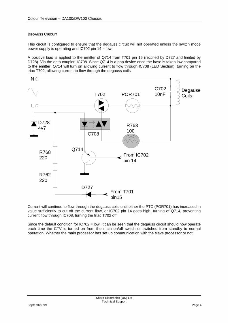
DEGAUSS CIRCUIT
This circuit is configured to ensure that the degauss circuit will not operated unless the switch modepower supply is operating and IC702 pin 14 = low.
A positive bias is applied to the emitter of Q714 from T701 pin 15 (rectified by D727 and limited byD728). Via the opto-coupler; IC708. Since Q714 is a pnp device once the base is taken low comparedto the emitter, Q714 will turn on allowing current to flow through IC708 (LED Section), turning on thetriac T702, allowing current to flow through the degauss coils.
Current will continue to flow through the degauss coils until either the PTC (POR701) has increased invalue sufficiently to cut off the current flow, or IC702 pin 14 goes high, turning of Q714, preventingcurrent flow through IC708, turning the triac T702 off.
Since the default condition for IC702 = low, it can be seen that the degauss circuit should now operateeach time the CTV is turned on from the main on/off switch or switched from standby to normaloperation. Whether the main processor has set up communication with the slave processor or not.
Colour Television – DA100/DW100 Chassis
Sharp Electronics (UK) LtdTechnical Support
September 99 Page 5
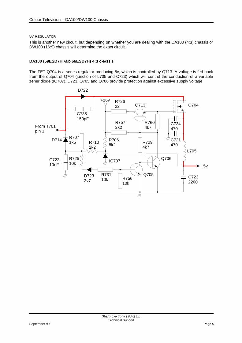
5V REGULATOR
This is another new circuit, but depending on whether you are dealing with the DA100 (4:3) chassis orDW100 (16:9) chassis will determine the exact circuit.
DA100 (59ESD7H AND 66ESD7H) 4:3 CHASSIS
The FET Q704 is a series regulator producing 5v, which is controlled by Q713. A voltage is fed-backfrom the output of Q704 (junction of L705 and C723) which will control the conduction of a variablezener diode (IC707). D723, Q705 and Q706 provide protection against excessive supply voltage.
D722
D714
IC707
D7232v7
Q705
Q706
Q704
+5v
+16v
From T701pin 1
Q713
L705
C7232200
C734470
C721470
R7604k7
R7294k7
R7572k2
R72622
R7068k2
R7102k2
R7071k5
R72510k
C72210nF
C735150pF
R73110k R756
10k
Colour Television – DA100/DW100 Chassis
Sharp Electronics (UK) LtdTechnical Support
September 99 Page 6
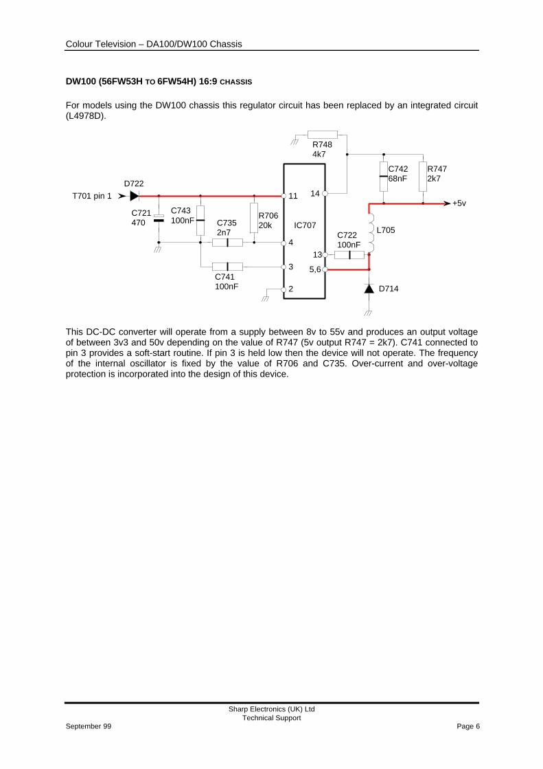
DW100 (56FW53H TO 6FW54H) 16:9 CHASSIS
For models using the DW100 chassis this regulator circuit has been replaced by an integrated circuit(L4978D).
This DC-DC converter will operate from a supply between 8v to 55v and produces an output voltageof between 3v3 and 50v depending on the value of R747 (5v output R747 = 2k7). C741 connected topin 3 provides a soft-start routine. If pin 3 is held low then the device will not operate. The frequencyof the internal oscillator is fixed by the value of R706 and C735. Over-current and over-voltageprotection is incorporated into the design of this device.
D722
T701 pin 1
4
11
3
2
14
5,6
13
C721470
C743100nF C735
2n7
R70620k
R7484k7
IC707C722100nF
L705
D714
C74268nF
R7472k7
+5v
C741100nF

Colour Television – DA100/DW100 Chassis
Sharp Electronics (UK) LtdTechnical Support
September 99 Page 7
CLASS D OUTPUT STAGES
The class ‘D’ output stages that Sharp Electronics have used since the introduction of the CS chassisare now incorporated into a specially design integrated circuit (TDA7480 = 10w output power,TDA7481 = 15w output power and TDA7482 = 25w output power). These devices are ideal for usewith TV Audio & Field output stages where high efficiency (low energy use) is required.
Sharp Electronics are currently using the TDA7480 for Audio and Frame outputs and the TDA7481 todrive the sub-woofer.
TDA7480 PIN FUNCTIONS
Pin No. Name Function123456789
1011121314151617181920
-VCC
-VCC
-VCC
OUTBOOTDIODEBOOTNCFEEDCAPFREQUENCYSGN-GNDINST-BY-MUTENC+VCC SIGNVREG+VCC POW-VCC
-VCC
-VCC
-VCC
NEGATIVE SUPPLY.NEGATIVE SUPPLY.NEGATIVE SUPPLY.PWM OUTPUTBOOTSTRAP DIODE ANODEBOOTSTRAP CAPACITORNOT CONNECTEDFEEDBACK INTEGRATING CAPACITANCESETTING FREQUENCY RESISTORSIGNAL GROUNDINPUTST-BY/ MUTE CONTROL PINNOT CONNECTEDPOSITIVE SIGNAL SUPPLY10V INTERNAL REGULATORPOSITIVE POWER SUPPLYNEGATIVE SUPPLY (De-coupled by 100nF)NEGATIVE SUPPLYNEGATIVE SUPPLYNEGATIVE SUPPLY
PIN 9 – FREQUENCY
The external components on this pin will determine the base frequency of the PWM section of this IC.Remember for the audio circuit the frequency will vary from the base frequency by the bandwidth ofthe audio signal (20kHz).
PIN 12 – MUTE/STANDBY FUNCTION
The voltage at pin 12 will determine the working condition of this device. A voltage of less than 0.8vwill tell the device to switch to standby, where a voltage between 1.8v to 2.5v will result in the outputbeing attenuated between 60 to 80 dB. For normal operation the voltage at pin 12 should be greaterthan 4v.
Colour Television – DA100/DW100 Chassis
Sharp Electronics (UK) LtdTechnical Support
September 99 Page 8
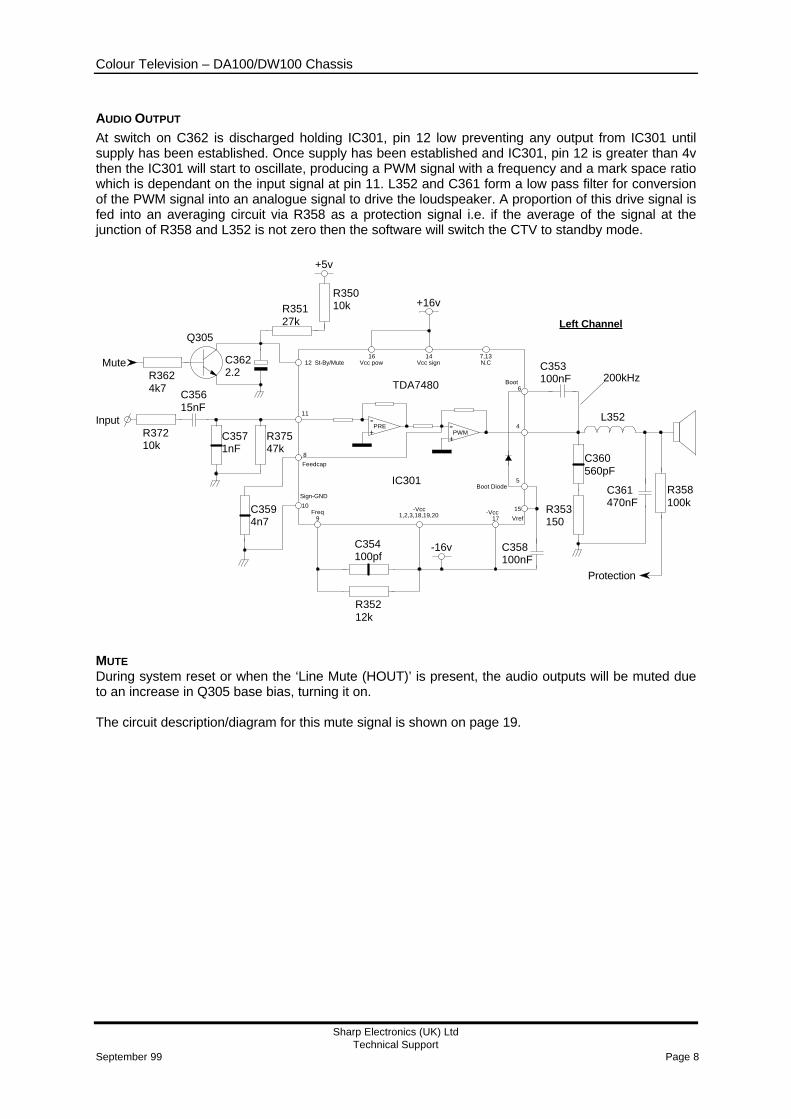
AUDIO OUTPUT
At switch on C362 is discharged holding IC301, pin 12 low preventing any output from IC301 untilsupply has been established. Once supply has been established and IC301, pin 12 is greater than 4vthen the IC301 will start to oscillate, producing a PWM signal with a frequency and a mark space ratiowhich is dependant on the input signal at pin 11. L352 and C361 form a low pass filter for conversionof the PWM signal into an analogue signal to drive the loudspeaker. A proportion of this drive signal isfed into an averaging circuit via R358 as a protection signal i.e. if the average of the signal at thejunction of R358 and L352 is not zero then the software will switch the CTV to standby mode.
MUTEDuring system reset or when the ‘Line Mute (HOUT)’ is present, the audio outputs will be muted dueto an increase in Q305 base bias, turning it on.
The circuit description/diagram for this mute signal is shown on page 19.
-+
PRE -+
PWM
16 14 7,1312
6
4
5
15
171,2,3,18,19,209
10
8
11
N.CVcc pow Vcc sign
Boot
Boot Diode
Vref-Vcc-VccFreq
Sign-GND
St-By/Mute
Feedcap
TDA7480
MuteR3624k7
Q305
C3622.2
InputR37210k
C35615nF
C3571nF
R37547k
C3594n7
C354100pf
R35212k
-16v C358100nF
C360560pF
R353150
C361470nF
Protection
C353100nF
+16vR35127k
R358100k
L352
Left Channel
200kHz
IC301
R35010k
+5v
Colour Television – DA100/DW100 Chassis
Sharp Electronics (UK) LtdTechnical Support
September 99 Page 9
FIELD OUTPUT
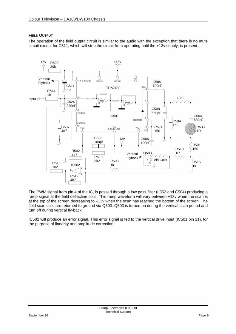
The operation of the field output circuit is similar to the audio with the exception that there is no mutecircuit except for C511, which will stop the circuit from operating until the +13v supply, is present.
The PWM signal from pin 4 of the IC, is passed through a low pass filter (L352 and C504) producing aramp signal at the field deflection coils. This ramp waveform will vary between +13v when the scan isat the top of the screen decreasing to –13v when the scan has reached the bottom of the screen. Thefield scan coils are returned to ground via Q503. Q503 is turned on during the vertical scan period andturn off during vertical fly-back.
IC502 will produce an error signal. This error signal is fed to the vertical drive input (IC501 pin 11), forthe purpose of linearity and amplitude correction.
-+
PRE -+
PWM
16 14 7,1312
6
4
5
15
171,2,3,18,19,209
10
8
11
N.CVcc pow Vcc sign
Boot
Boot Diode
Vref-Vcc-VccFreq
Sign-GND
St-By/Mute
Feedcap
TDA7480
Input
R5441k
C524330nF
C5074n7
C503100pf
R5108k2
-13v C506100nF
C508560pF
R511150
C504680nF
C505100nF
+13vR50939k
L352
C5341nF
Field CoilsR5161k
R5181R
R501150
R5331R
Q503VerticalFlyback
C5112.2
VerticalFlyback
R5031k
R5024k7
IC502
R5124k7
R5151k2
1
2
3
IC501
+5v
Colour Television – DA100/DW100 Chassis
Sharp Electronics (UK) LtdTechnical Support
September 99 Page 10
V Prot Signal
VERTICAL FLY-BACK
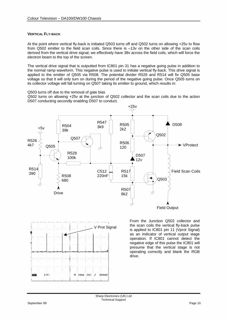
At the point where vertical fly-back is initiated Q503 turns off and Q502 turns on allowing +25v to flowfrom Q502 emitter to the field scan coils. Since there is –13v on the other side of the scan coilsderived from the vertical drive signal, we effectively have 38v across the field coils, which will force theelectron beam to the top of the screen.
The vertical drive signal that is outputted from IC801 pin 31 has a negative going pulse in addition tothe normal ramp waveform. This negative pulse is used to initiate vertical fly-back. This drive signal isapplied to the emitter of Q505 via R508. The potential divider R526 and R514 will fix Q505 basevoltage so that it will only turn on during the period of the negative going pulse. Once Q505 turns onits collector voltage will fall turning on Q507 taking its emitter to ground, which results in:
Q503 turns off due to the removal of gate biasQ502 turns on allowing +25v at the junction of Q502 collector and the scan coils due to the actionD507 conducting secondly enabling D507 to conduct.
From the Junction Q502 collector andthe scan coils the vertical fly-back pulseis applied to IC801 pin 11 (Vprot Signal)as an indicator of vertical output stageoperation. If IC801 cannot detect thenegative edge of this pulse the IC801 willpresume that the vertical stage is notoperating correctly and blank the RGBdrive.
+25v
+5v
VProtect
Field Scan Coils
R5264k7
R514390
R508680
Q505
R528100k
R50439k
Q507
R5473k9
C512220nF
R5052k2
R506120
R51715k
R5078k2
D50712v
Q502
D508
Q503
Drive
Field Output

Colour Television – DA100/DW100 Chassis
Sharp Electronics (UK) LtdTechnical Support
September 99 Page 11
VIDEO AND SYNC PROCESSOR
This IC is a member of the ‘Micronas’ VDP 31xxB IC family, which are high-quality video processorsAllowing the economic integration of features in all classes of TV sets. The VDP 31xxB family isbased on functional blocks contained in the two previous chips form Micronas:
VPC 3200A Video ProcessorDDP 3300A Display and Deflection Processor
VDP 31xxB contains the entire video, display, and deflection processing for 4:3 and 16:9 CTV’soperating at either 50 or 60Hz featuring:
2H adaptive Comb-filterScan Velocity Modulator.1H Comb-filterColour Transient Improvement.RGB InsertionTube ControlProgrammable RGB Matrix4 composite inputs (one for S-VHS)Composite video & sync outputHorizontal scaling (0.25 to 4)Panorama visionBlack level expanderDynamic peakingSoft-limiter (gamma correction)Picture frame generatorHigh-performance H/V deflectionSeparate ADC for tube measurementsEHT compensationOne 20.25 MHz crystal (for all systems), few external componentsEmbedded RISC controller (80 MIPS)I 2 C-Bus InterfaceSingle 5 V power supply
DESCRIPTION
ANALOGUE FRONT-END
This block provides the analogue interfaces to all video inputs and mainly carries out analogue-todigital conversion for the following digital video processing.
Most of the functional blocks in the front-end are digitally controlled (clamping, AGC, and clock-DCO).The control loops are closed by the Fast Processor (‘FP’) embedded in the decoder.
INPUT SELECTOR
Up to five analogue inputs can be connected. Four inputs are for input of composite video or S-VHSluma signal. These inputs are clamped to the sync back porch and are amplified by a variable gainamplifier. One input is for connection of S-VHS chrominance signal. This input is internally biased andhas a fixed gain amplifier.
CLAMPING
The composite video input signals are AC coupled to the IC. The clamping voltage is stored on thecoupling capacitors and is generated by digitally controlled current sources. The clamping level is theback porch of the video signal. S-VHS chroma is also AC coupled. The input pin is internally biased tothe centre of the ADC input range.
Colour Television – DA100/DW100 Chassis
Sharp Electronics (UK) LtdTechnical Support
September 99 Page 12
AUTOMATIC GAIN CONTROL
A digitally working automatic gain control adjusts the magnitude of the selected base-band by +6/–4.5dB in 64 logarithmic steps to the optimal range of the ADC. The gain of the video input stage includingthe ADC is 213 steps/V with the AGC set to 0 dB.
ANALOGUE-TO-DIGITAL CONVERTERS
Two ADCs are provided to digitise the input signals. Each converter runs with 20.25 MHz and has 8bit resolution. An integrated band-gap circuit generates the required reference voltages for theconverters.
DIGITALLY CONTROLLED CLOCK OSCILLATOR
The clock generation is also a part of the analogue front end. The crystal oscillator is controlleddigitally by the control processor; the clock frequency can be adjusted within ±150 ppm.
ANALOGUE VIDEO OUTPUT
The input signal of the Luma ADC is available at the analogue video output pin. A source followermust buffer the signal at this pin. The output voltage is 2 V, thus the signal can be used to drive a 75Ωline. The magnitude is adjusted with an AGC in 8 steps together with the main AGC.
AVERAGE BEAM CURRENT LIMITING
The average beam current limiter (BCL) uses the sense input for the beam current measurement. TheBCL uses a different filter to average the beam current during the active picture. The filter bandwidthis approximately. 2 kHz.
The beam current limiter has an automatic offset adjustment that is active two lines before the firstcut-off measurement line.
The beam current limiter allows the setting of a threshold current. If the beam current is above thethreshold, the excess current is low-pass filtered and used to attenuate the RGB outputs by adjustingthe white-drive multipliers for the internal (digital) RGB signals, and the analogue contrast multipliersfor the analogue RGB inputs, respectively.
The lower limit of the attenuator is programmable, thus a minimum contrast can always be set. Duringthe CRT measurement, the ABL attenuation is switched off. After the white drive measurement line ittakes 3 lines to switch back to BCL limited drives and brightness.
PROTECTION CIRCUITRY
‘Vertical fly-back’ and the ‘Safety’ inputs provide picture tube and drive stage protection.
Vertical fly-back; This pin searches for a negative edge in every field, otherwise the RGBdrive signals are blanked. Drive shutoff during fly-back: this feature can beselected by software.
Safety; Input pin: this input has two thresholds. Between zero and the lowerthreshold, normal functioning takes place. Between the lower and thehigher threshold, the RGB signals are blanked. Above the higherthreshold, the RGB signals are blanked and the horizontal drive is shut off.
Both thresholds have a small hysteresis. The main oscillator and thehorizontal drive circuitry are run from a separate (standby) power supplyand are already active while the TV set is powering up.
Note:In the DA100 and DW100 chassis the standby supply pin is connected to VCC.
SCAN VELOCITY MODULATION OUTPUT
This output delivers the analogue SVM signal. The D/A converter is a current sink like the RGB D/Aconverters. At zero signal level the output current is 50% of the maximum output current.

Colour Television – DA100/DW100 Chassis
Sharp Electronics (UK) LtdTechnical Support
September 99 Page 13
PICTURE ROTATION
Due to the width of a 16:9 CRT the horizontal tilt of the picture can be influence by external magneticfields.
To overcome this problem, an extra coil is fitted around the CRT, which is connected between thejunction of Q1603/Q1604 emitter and ground.
The microprocessor (IC1001) will output a PWM signal from pin 55. This signal is then passedthrough a LPF and fed to an error amplifier (IC601). The output from this error amp can swing from apositive to a negative voltage depending on the mark space ratio of the PWM signal from IC1001.
Under normal conditions (CRT is not effected by external magnetic fields) there will be no output fromthe error amplifier, therefore, both Q1603 and Q1604 are turned off causing no current to flow throughthe coil around the CRT neck. However if the output from the error amplifier is positive then Q1603will turn on allowing current to flow from the +13v rail, through the coil to ground. If the error amplifieroutput is negative going then Q1604 will turn on, allowing current to flow from ground to the –13v rail.
The end user has control of this adjustment via the picture menu.
NoteThe location of this circuit can vary between 66cm models (Located on CRT base) and 76cmmodels (located on sub PWB).
+
-1kHz PWMIC1001, pin 55
R162010k
R1619100k
C160810
R16172k2
D16072v4
C160910
R1618100k
R1616100k
C1610100nF
IC1601
C161110nF
R16151M
R1624100
R1622470
Q1603
Q1604
-13vR1623100
R1621100
+13v
C1613220
C1612220
Tilt Coils
Colour Television – DA100/DW100 Chassis
Sharp Electronics (UK) LtdTechnical Support
September 99 Page 14
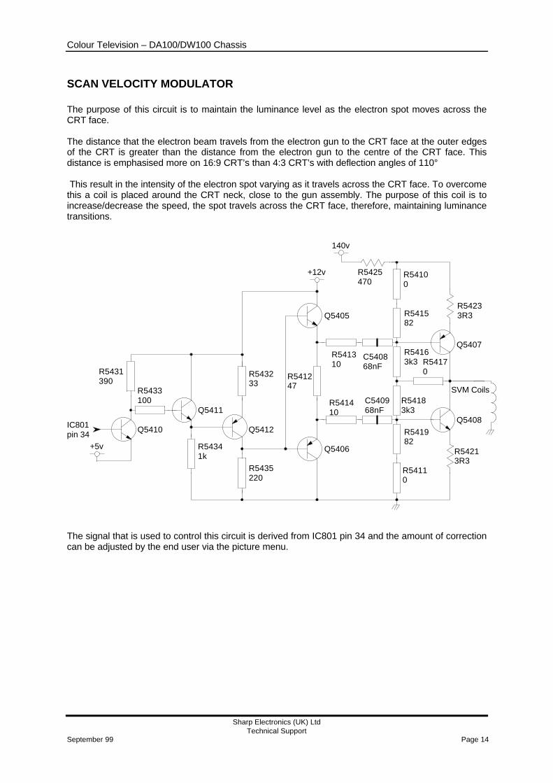
SCAN VELOCITY MODULATOR
The purpose of this circuit is to maintain the luminance level as the electron spot moves across theCRT face.
The distance that the electron beam travels from the electron gun to the CRT face at the outer edgesof the CRT is greater than the distance from the electron gun to the centre of the CRT face. Thisdistance is emphasised more on 16:9 CRT’s than 4:3 CRT’s with deflection angles of 110°
This result in the intensity of the electron spot varying as it travels across the CRT face. To overcomethis a coil is placed around the CRT neck, close to the gun assembly. The purpose of this coil is toincrease/decrease the speed, the spot travels across the CRT face, therefore, maintaining luminancetransitions.
The signal that is used to control this circuit is derived from IC801 pin 34 and the amount of correctioncan be adjusted by the end user via the picture menu.
Q5410
R5431390
R5433100
Q5411
Q5412
R543233
R54341k
R5435220
Q5406
Q5405
R541247
R541310
C540868nF
R541410
C540968nF
R54100
R541582
R54163k3
R54183k3
R541982
R54110
R54213R3
Q5408
Q5407
R54233R3
R54170
+5v
140v
+12v R5425470
IC801pin 34
SVM Coils

Colour Television – DA100/DW100 Chassis
Sharp Electronics (UK) LtdTechnical Support
September 99 Page 15
LINE OUTPUT STAGEAs in previous chassis a transformer-less driver circuit has been used, with the driver stage obtainingit’s run voltage from the fly-back transformer, T601.At switch on +8v from the power supply is applied to Q603 collector via R605 and Q602 collector viaR628 and R608. At the same time –16v is applied to Q602 emitter via R619. Horizontal drive fromIC801 is applied to the base of Q603, This will cause Q603 to switch, which in turn switches the lineoutput transistor Q601, producing an e.m.f on pins 6 and 10 of the fly-back transformer T601. Thee.m.f at pin 10 is rectified by D611 to produce the positive run voltage and the e.m.f at pin 6 isrectified by D610 to produce the negative run voltage.
With this type of driver circuit, it is essential that the circuit is started softly, otherwise transient pulsescan damage the line output transistor. This is achieved by doubling the horizontal drive frequency;which effectively reduces Q601 on time, until the run voltage has been established.
In addition to producing the EHT, focus, screen voltage and horizontal scan from the fly-backtransformer T601, the +/-13v rails for the field output are produced at pins 5 and 9. D609 rectifies thee.m.f at pin 9 producing the +13v and D608 rectifies the e.m.f at pin 5 producing the –13v.
Horizontal fly-back pulses (HFB) from pin 1 is fed to IC801 for both timing purposes and safety(prevents excesses EHT), HFB is also rectified by D610 to produce +25v for vertical fly-back. Fromthe primary winding (pin 7) the HT is stepped up and rectified by D621 to produce the HT required bythe CRT drive circuit. Finally a negative going voltage is fed from pin 8 to the protection circuit. Thisvoltage represents the beam current. The greater the beam current (Bright Raster) the greater thisvoltage would be in a negative direction. This negative voltage is then fed to the IC1001 pin 95 viaD622 and Q606. Once this voltage has exceeded safe working levels IC1001 pin 95 will go lowswitching the CTV to standby.
EHT
East/West Circuit
+8V
-16v
Q601
LineDrive
D610
Focus
Screen
ABL
HFB
+25v
+13v
-13v
10
1
956
8
13
+150v(CRT Base)
+150v
2
7
3
4
F602
F601
D609
D608
D510R61722
R6245R6
D604
D603C60112nF
C61027nF
L609
R61222
C607330
R619560
R642470
R6013k9
Q602
Q603
R605470
R60712k
R6281k
R6081k
L606
D611
R6231
R61722
D621
Colour Television – DA100/DW100 Chassis
Sharp Electronics (UK) LtdTechnical Support
September 99 Page 16
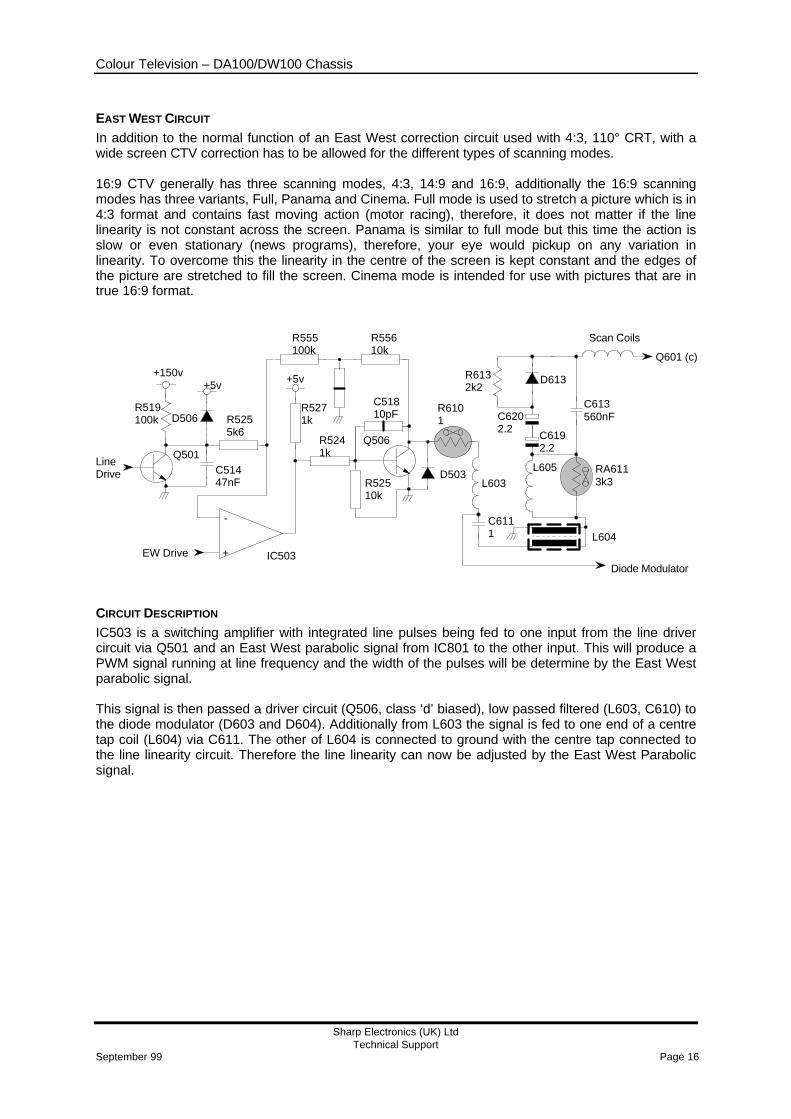
EAST WEST CIRCUIT
In addition to the normal function of an East West correction circuit used with 4:3, 110° CRT, with awide screen CTV correction has to be allowed for the different types of scanning modes.
16:9 CTV generally has three scanning modes, 4:3, 14:9 and 16:9, additionally the 16:9 scanningmodes has three variants, Full, Panama and Cinema. Full mode is used to stretch a picture which is in4:3 format and contains fast moving action (motor racing), therefore, it does not matter if the linelinearity is not constant across the screen. Panama is similar to full mode but this time the action isslow or even stationary (news programs), therefore, your eye would pickup on any variation inlinearity. To overcome this the linearity in the centre of the screen is kept constant and the edges ofthe picture are stretched to fill the screen. Cinema mode is intended for use with pictures that are intrue 16:9 format.
CIRCUIT DESCRIPTION
IC503 is a switching amplifier with integrated line pulses being fed to one input from the line drivercircuit via Q501 and an East West parabolic signal from IC801 to the other input. This will produce aPWM signal running at line frequency and the width of the pulses will be determine by the East Westparabolic signal.
This signal is then passed a driver circuit (Q506, class ‘d’ biased), low passed filtered (L603, C610) tothe diode modulator (D603 and D604). Additionally from L603 the signal is fed to one end of a centretap coil (L604) via C611. The other of L604 is connected to ground with the centre tap connected tothe line linearity circuit. Therefore the line linearity can now be adjusted by the East West Parabolicsignal.
Q601 (c)
Scan Coils
+5v
Diode Modulator
L604
RA6113k3
L605
C6192.2
C6202.2
C613560nF
D613R6132k2
L603
C6111
D503
R6101
C51810pF
Q506
R52510k
R5241k
R5271k
+
-
EW Drive
LineDrive
+150v+5v
D506R519100k
Q501C51447nF
R5255k6
R555100k
R55610k
IC503
Colour Television – DA100/DW100 Chassis
Sharp Electronics (UK) LtdTechnical Support
September 99 Page 17
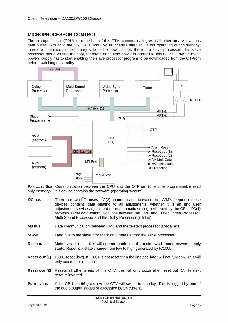
MICROPROCESSOR CONTROLThe microprocessor (CPU) is at the hart of this CTV, communicating with all other area via variousdata buses. Similar to the CS, CA10 and CW100 chassis this CPU is not operating during standby,therefore contained in the primary side of the power supply there is a slave processor. This slaveprocessor has a volatile memory, therefore each time power is applied to this CTV the switch modepowers supply has to start enabling the slave processor program to be downloaded from the OTPrombefore switching to standby.
PARALLEL BUS Communication between the CPU and the OTProm (one time programmable readonly memory). This device contains the software (operating system)
I2C BUS There are two I2C buses, I2C(2) communicates between the NVM’s (eeprom), thesedevices contains data relating to all adjustments, whether it is an end useradjustment, service adjustment or an automatic setting performed by the CPU. I2C(1)provides serial data communications between the CPU and Tuner, Video Processor,Multi Sound Processor and the Dolby Processor (if fitted).
M3 BUS Data communication between CPU and the teletext processor (MegaText)
SLAVE Data bus to the slave processor an a data us from the slave processor.
RESET IN Main system reset, this will operate each time the main switch mode powers supplystarts. Reset is a state change from low to high generated by IC1005.
RESET OUT (1) IC801 reset (low). If IC801 is not reset then the line oscillator will not function. This willonly occur after reset in.
RESET OUT (2) Resets all other areas of this CTV, this will only occur after reset out (1). Teletextreset is inverted.
PROTECTION If the CPU pin 96 goes low the CTV will switch to standby. This is trigged by one ofthe audio output stages or excessive beam current.
DolbyProcessor
Video/SyncProcessor
TunerMulti-SoundProcessor
I2C Bus (2)
I2S Bus
NVM(eeprom)
NVM(eeprom)
I2C Bus (1)
SlaveProcessor
MegaText
M3 Bus
IC1001(CPU)
OTP
Main ResetReset out (1)Reset out (2)AV Link DataAV Link Clock
AFT-1AFT-2
IF
IC2028
Protection
PageStore
Colour Television – DA100/DW100 Chassis
Sharp Electronics (UK) LtdTechnical Support
September 99 Page 18
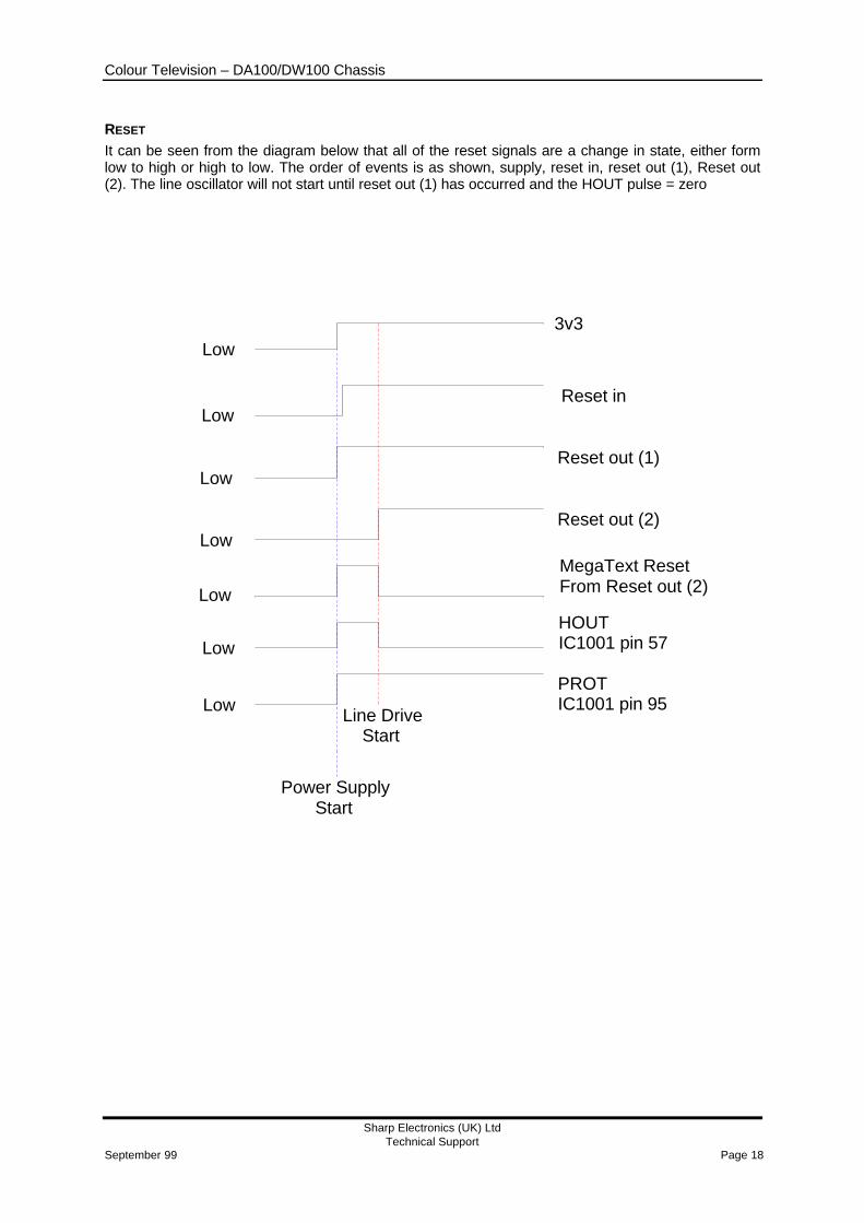
RESET
It can be seen from the diagram below that all of the reset signals are a change in state, either formlow to high or high to low. The order of events is as shown, supply, reset in, reset out (1), Reset out(2). The line oscillator will not start until reset out (1) has occurred and the HOUT pulse = zero
3v3
Reset in
Reset out (1)
Reset out (2)
MegaText ResetFrom Reset out (2)
Low
Low
Low
Low
HOUTIC1001 pin 57Low
Low
Low
Power Supply Start
Line Drive Start
PROTIC1001 pin 95
Colour Television – DA100/DW100 Chassis
Sharp Electronics (UK) LtdTechnical Support
September 99 Page 19
PROTECTION
MICROPROCESSOR
AUDIO OUTPUT
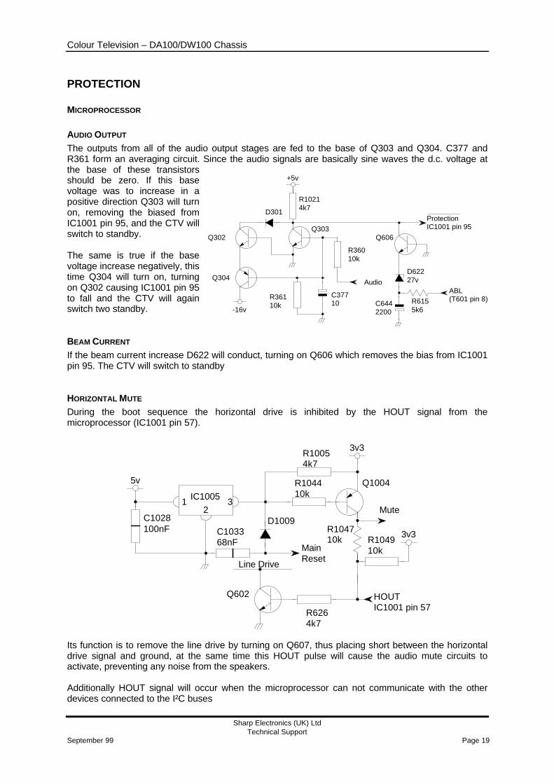
The outputs from all of the audio output stages are fed to the base of Q303 and Q304. C377 andR361 form an averaging circuit. Since the audio signals are basically sine waves the d.c. voltage atthe base of these transistorsshould be zero. If this basevoltage was to increase in apositive direction Q303 will turnon, removing the biased fromIC1001 pin 95, and the CTV willswitch to standby.
The same is true if the basevoltage increase negatively, thistime Q304 will turn on, turningon Q302 causing IC1001 pin 95to fall and the CTV will againswitch two standby.
BEAM CURRENT
If the beam current increase D622 will conduct, turning on Q606 which removes the bias from IC1001pin 95. The CTV will switch to standby
HORIZONTAL MUTE
During the boot sequence the horizontal drive is inhibited by the HOUT signal from themicroprocessor (IC1001 pin 57).
Its function is to remove the line drive by turning on Q607, thus placing short between the horizontaldrive signal and ground, at the same time this HOUT pulse will cause the audio mute circuits toactivate, preventing any noise from the speakers.
Additionally HOUT signal will occur when the microprocessor can not communicate with the otherdevices connected to the I²C buses
ProtectionIC1001 pin 95
-16v
Audio
+5v
Q303
R10214k7
Q302
Q304
D301
R36110k
C37710
R36010k
Q606
D62227v
R6155k6
C6442200
ABL(T601 pin 8)
12
3
100nF
5v
C1028
IC1005
MainReset
HOUTIC1001 pin 57
3v3
Mute
Q1004
R104710k R1049
10k
R104410k
R10054k7
C103368nF
3v3
D1009
R6264k7
Q602
Line Drive
Colour Television – DA100/DW100 Chassis
Sharp Electronics (UK) LtdTechnical Support
September 99 Page 20
VIDEO/SYNC PROCESSOR
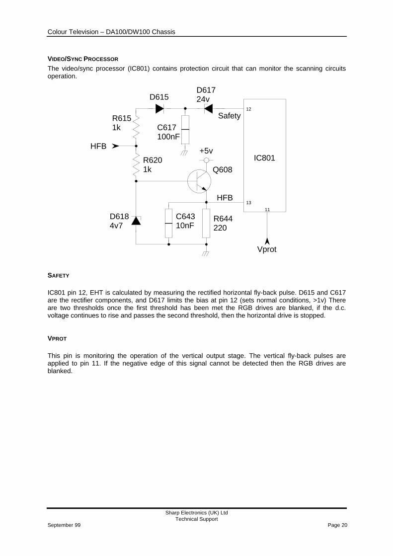
The video/sync processor (IC801) contains protection circuit that can monitor the scanning circuitsoperation.
SAFETY
IC801 pin 12, EHT is calculated by measuring the rectified horizontal fly-back pulse. D615 and C617are the rectifier components, and D617 limits the bias at pin 12 (sets normal conditions, >1v) Thereare two thresholds once the first threshold has been met the RGB drives are blanked, if the d.c.voltage continues to rise and passes the second threshold, then the horizontal drive is stopped.
VPROT
This pin is monitoring the operation of the vertical output stage. The vertical fly-back pulses areapplied to pin 11. If the negative edge of this signal cannot be detected then the RGB drives areblanked.
+5v
Q608
Safety
HFB
HFB
D6184v7
C64310nF
R644220
C617100nF
D61724vD615
R6151k
R6201k
IC801
12
13
11
Vprot

Colour Television – DA100/DW100 Chassis
Sharp Electronics (UK) LtdTechnical Support
September 99 Page 21
A V LinkThis CTV chassis has the capability of directly controlling a VCR via the SCART socket or the VCRcontrolling the CTV. In either chase the VCR must be compatible with the ‘A V Link’ system, alsoduring the installation of the CTV and VCR you will decide whether it is the CTV or VCR which hasoverall control.
Data from the CTV to VCR is from IC1001 pin 16 via Q1005 and is outputted from pin 10 either AV-1or RGB SCART sockets. Data from VCR is from the same SCART connection but this time it is fedinto IC1001 pin 92 via D1003. D411 provides protection from excess voltage being applied to theSCART sockets.
In addition to this data is outputted at AV-1 SCART pin 12, this data is intended to be read by acomputer, enhancing fault finding procedures. Currently this system is still being developed, moredetails will be given when the software and interface becomes available.
IC1001
92
16
21
R1023220
R103310k
+5v
R103227k
R102510k
+5v
R10354k7
D4115v6
Q1005
D1003
AV-1 Scartpin 12
AV-1 Scartpin 10
RGB Scartpin 10
Service Data