50 YEARS OF LASER CUTTING - AILU · 3 ISSUE 84 SPRING 2017 CONTENTS HIGHLIGHTS... ASSOCIATION NEWS...
36
1 ISSUE 84 SPRING 2017 IN THIS ISSUE: Nuclear Laser Welding Laser 3D Polishing Surface Texturing Ti:Sapphire Machining Transparent Materials Glass Processing ISSUE 84 SPRING 2017 THE LASER USER 50 YEARS OF LASER CUTTING: ADVANCED APPLICATIONS MATERIALS & SOURCES
Transcript of 50 YEARS OF LASER CUTTING - AILU · 3 ISSUE 84 SPRING 2017 CONTENTS HIGHLIGHTS... ASSOCIATION NEWS...

1
ISSUE 84 SPRING 2017
IN THIS ISSUE:
Nuclear Laser Welding
Laser 3D Polishing
Surface Texturing
Ti:Sapphire Machining
Transparent Materials
Glass Processing
ISSUE 84 SPRING 2017THE
LASER USER
50 YEARS OF LASER CUTTING: ADVANCED APPLICATIONS MATERIALS & SOURCES

2
ISSUE 84 SPRING 2017
THE LASER USER
Editor: Dave MacLellanSub-Editor: Catherine Rose
ISSN 1755-5140
© 2017 – Association of Industrial Laser Users
The Laser User is the house magazine of the Association of Industrial Laser Users. Its primary aim is to disseminate technical information and to present the views of its members. The Editor reserves the right to edit any submissions for space and other considerations.
Authors retain the right to extract, in part or in whole, their material for future use. The Laser User is published quarterly in February, May, August and November by AILU for its members and is available in print or online.
Editorial Board for this issue:
Ric Allott STFCJon Blackburn TWINicholas Blundell MTCEmmanuel Brousseau Cardiff University Stefan Dimov University of BirminghamJonathan Lawrence Coventry UniversityLin Li University of ManchesterMark Millar Essex LaserNadeem Rizvi Laser MicromachiningNeil Sykes MicronanicsMark Thompson IPG Photonics
Association of Industrial Laser UsersOxford House 100 Ock StreetAbingdon OxfordshireOX14 5DH
Tel: +44 (0) 1235 539595E-mail: [email protected]: www.ailu.org.uk
AILU STEERING COMMITTEE 2016-17
President: Ric Allott (STFC)Vice President: Lin Li (University of Manchester)Exec. Director: Dave MacLellan (Anode Marketing)
Elected until 2019Duncan Hand (Heriot-Watt University) Louise Jones (KTN)Jonathan Lawrence (Coventry University) Ian White (Yamazaki Mazak)
Elected until 2018Paul Goodwin (TWI)Roger Hardacre (ALT)Tony Jones (Cyan Tec Systems)Adrian Norton (thinklaser)
Elected until 2017Simon Andrews (Fraunhofer CIP)Louise Geekie (Croft Additive Manufacturing)Stuart McCulloch (SPI Lasers)
Co-optedJon Blackburn (TWI) Adam Clare (University of Nottingham)Mark Millar (Essex Laser)Stan Wilford (IPG Photonics)
Past presidents and founder members are also able to attend committee meetings. Anyone wishing to join the AILU Steering Committee please contact the Executive Director.
Cover image: TWI has recently completed the demonstration phase of the project LaserSnake2. After two years of trials and planning, permission was given to take the new, long reach snake-arm robot (developed in the project by OC Robotics) and combine it with cutting techniques developed by TWI, ULO Optics, and Laser Optical Engineering, to reduce the size of a large radioactive stainless steel dissolver vessel.
Image courtesy of TWI Ltd
WELCOME TO NEW CORPORATE MEMBER
TTP James Lazarus [email protected]
ADVERTISING ENQUIRIES+44 (0) 1235 [email protected]
Advertising rates at:http://bit.ly/AILU_Media_Guide_2017
3
ISSUE 84 SPRING 2017
CONTENTS
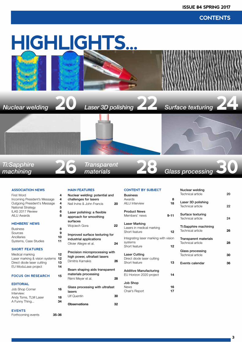
HIGHLIGHTS...
ASSOCIATION NEWS
First Word 4 Incoming President’s Message 4Outgoing President's Message 4 National Strategy 5ILAS 2017 Review 6AILU Awards 8 MEMBERS’ NEWS
Business 8Sources 9Ancillaries 10 Systems, Case Studies 11 SHORT FEATURES
Medical marking 12 Laser marking & vision systems 12Direct diode laser cutting 13EU ModuLase project 14
FOCUS ON RESEARCH 15
EDITORIAL
Job Shop Corner 16Interview: Andy Toms, TLM Laser 18 A Funny Thing... 34
EVENTSForthcoming events 35-36
MAIN FEATURES
Nuclear welding: potential and challenges for lasersNeil Irvine & John Francis 20
Laser polishing: a flexible approach for smoothing surfaces Wojciech Gora 22
Improved surface texturing for industrial applicationsOlivier Allegre et al. 24
Precision microprocessing with high power, ultrafast lasers Dimitris Karnakis 26
Beam shaping aids transparent materials processing Rémi Meyer et al. 28
Glass processing with ultrafast lasers Ulf Quentin 30 Observations 32
CONTENT BY SUBJECT
BusinessAwards 8AILU Interview 18 Product News Members’ news 9-11
Laser MarkingLasers in medical marking Short feature 12
Integrating laser marking with vision systems Short feature 12
Laser CuttingDirect diode laser cuttingShort feature 13
Additive ManufacturingEU Horizon 2020 project 14
Job Shop News 16Chair’s Report 17
Nuclear welding Technical article 20
Laser 3D polishingTechnical article 22
Surface texturingTechnical article 24
Ti:Sapphire machining Technical article 26
Transparent materialsTechnical article 28
Glass processingTechnical article 30 Events calendar 36
30
24
28
22
26
20Nuclear welding
Ti:Sapphire machining
Laser 3D polishing
Transparent materials
Surface texturing
Glass processing

4
ISSUE 84 SPRING 2017
FIRST WORDI hope that you enjoyed ILAS in March if you were able to make it? If not, you missed out on a great event, and you can find some of the material in this issue of the magazine. Feedback has been very good with 100% of those responding to our questionnaire saying they would recommend ILAS to their colleagues. As ever, it was a great opportunity to make new connections and renew existing ones – but there simply wasn’t enough time to talk to everyone!
The next few months will involve a lot of travel for me - visits to Czech Republic, Japan, France and Germany between now and the end of June. AILU is not just for UK members, and we look forward to welcoming our non-UK members to our first workshop located in France – Lasers in Biotechnology – which takes place on June 15 in Lyon. If you are interested in applications in this area, be sure to come along as a delegate or exhibitor.
Those with an interest in Laser Precision Microfabrication should keep in mind that June 2018 will see AILU (and the UK) hosting LPM 2018 at Heriot Watt, Edinburgh. This conference and exhibition will be bigger than ILAS – lasting for 4 days and having many more visitors from Japan and Germany. Take advantage of the opportunity to attend this “local event” – it promises to be spectacular.
Later in June I am looking forward to the opportunity to make new connections and meet up with old friends and colleagues at Laser World of Photonics in Munich. I remember well the first time I visited in 1991, and now for me it is a “must visit” opportunity to network with those people I only see at such events. If you are there, let me know and we can meet up.
On June 8th there will be another UK General Election, and the need for me to register for a postal vote – I am often asked for comments on Brexit, so please do let me have your thoughts so we can represent the wider views of our members appropriately.
Dave MacLellan
AILU Executive Director
[email protected] 07473 121142
ASSOCIATION NEWS
INCOMING PRESIDENT'S MESSAGEI am greatly honoured to have this opportunity to serve as the next President of the Association of Industrial Laser Users. I will do my best to ensure AILU continues to grow and thrive. I would like to thank Ric Allott for his excellent job leading AILU for the last two years and Dave MacLellan (Executive Director) for the successful delivery of AILU agendas.
Over the last two years AILU has organised two successful ILAS conferences (2015, 2017), has produced a new logo, a new AILU magazine and e-newsletter style, and run a number of workshops. AILU is also involved in developing the UK’s national strategy on laser based manufacturing. A new website design is in progress. The key strength of AILU is its close association with industries, particularly the UK laser job-shop industry.
The things that I would like to put on the AILU agenda over the next two years include:
• Increasing international collaborations (e.g. with the Laser Institute of America, Japan Laser Processing Society, German Scientific Laser Society (WLT), Chinese Laser Processing Society and SPIE, OSA) and organise joint events, conferences and workshops. The Laser Precision Microfabrication (LPM) conference to be held in 2018 in the UK will be run jointly with the Japan Laser Processing Society.
• Increasing number of end-user participations in AILU, by organising end-user focused industry sector theme-based workshops and events, demonstrating clear benefits to the end users.
• Increasing student participation in AILU, by developing an AILU student community and organising student focused events.
• Developing an Executive Forum for the CEO, CTOs and group leaders of industry and academic institutions to meet and discuss key issues in laser based manufacturing facing us today and in the future.
I will work closely with our incoming Vice President, Jonathan Blackburn (TWI), Dave MacLellan and AILU team, AILU Executive Committee members, special interest group leaders, workshop leaders and our AILU members and non-members to develop and deliver the AILU agenda for the next two years.
OUTGOING PRESIDENT’S MESSAGEWelcome to the latest edition of The Laser User. I have to admit that I am writing this with a degree of sadness as this will be my last President’s Message. I cannot believe how fast the last two years have gone!
I wish to first convey my thanks to the AILU team and to you our members for making ILAS 2017 such a fantastic success. I thoroughly enjoyed our two days out in Grantham and I received lots of positive feedback from the delegates with whom I managed to speak. I am sure that ILAS will continue to go from strength to strength and our strategy to reach out further beyond the UK’s shores will only serve to enhance the conference in future years.
As you will know, AILU has been working alongside the EPSRC CIM and with our community in producing “Lasers for Productivity - a UK Strategy” and the first “pre-release” version of this was distributed at ILAS in March. We have since received some very valuable feedback and are getting close to a final version for general release. There is a short article in this magazine that summarises the key points from the Strategy and highlights the actions to take forward. With the recent publication of the
Governments’ “Building our Industrial Strategy” green paper, the release of our strategy really is excellent timing. As you read this I will have stood down from the presidency of AILU and handed over to the capable hands of new President, Prof Lin Li and Vice-President Jon Blackburn but I will be still be working with the team in finalising and supporting the delivery of the strategy.
Finally, I would like to say what a great privilege it has been over the past 4 years as both Vice-President working with Neil Main and Mike Green and subsequently as President overseeing the transition from the Green to the MacLellan era. Lasers and laser processing are in my blood and I remain very passionate about our sector and community. AILU I know will continue to build and serve you in the best ways possible. I wish you all every success in the future.
Ric Allott [email protected]

5
ISSUE 84 SPRING 2017
NATIONAL STRATEGY
This article provides a summary of a new UK Strategy that has been developed for and by UK industry in the field of Laser Processing for Manufacturing. This audience does not require a definition of what is meant by laser processing but for the sake of completeness it includes the use of lasers to mark, cut, scribe, build, join or modify components in any form.
The strategy takes input from a broad cross-section of UK manufacturing sectors in collaboration with:-
• Industrial manufacturers, sub-contractor manufacturers and suppliers.
• UK laser and system manufacturers and associated supply chains.
• Association of Industrial Laser Users (AILU).
• EPSRC Centre for Innovative Manufacturing. in Laser Based Production Processes.
• Knowledge Transfer Network (KTN).
• Photonics Leadership Group (PLG).
Although the process for developing this strategy was started over 2 years ago, the timing of the release (full public release within the next month or two) could not be better as it coincides with the Governments green paper published in January 2017 “Building our Industrial Strategy”. Laser processing presents a huge opportunity for vastly improved productivity, lower processing costs and waste materials together with the potential to innovate with new materials and processes. In short High Value Manufacturing in the UK needs lasers and laser processes.
The strategy aims to position laser based processes as the norm for UK companies and not the unusual.
The strategy sets out a vision for UK manufacturing, benchmarks the current state of the industry then looks at barriers to the uptake of lasers, opportunities for growth and finally provides a series of recommendations and sets out an action plan.
Surprisingly perhaps, UK manufacturers lag significantly behind our leading competitors in the adoption of laser processing, purchasing for example just 8% of the high power laser processing systems bought by German manufacturing companies. This is in stark contrast to the UK’s leading position in laser and process development. UK laser and systems manufacturers export over 80% of their products, which though healthy for the companies concerned is also a reflection of the limited uptake of such systems by the UK.
Why is this the case? Our work has shown that the biggest barrier to uptake is the shortage of skilled staff, most critically at the engineering and technician level. Skills and the awareness of the impact of laser processing are the highest priority action areas identified in the strategy.
The next most pressing issue identified was access to finance to allow investment in new equipment and skilled resource. Certainly new and innovative, flexible financing schemes are required. Also, despite the already significant “toolbox” of lasers and processes available today and the advantages they provide there is still a requirement to develop new technology, lasers and processing methods in order that the next generation of materials may be realised whilst constantly improving the flexibility, precision, reliability and predictability of processing.
Five key recommendations were identified in the strategy to address the issues and challenges identified. These were:-
1. Skills & Training -significantly increasing vocational training, building laser processing into Further Education and funding more apprenticeships.
2. Access to Finance – easing the purchase of capital equipment, perhaps through Innovate UK loans or other flexible and innovative funding models.
3. Process Demonstration & Customisation for SMEs – demonstration of proof-of-concept and proof-of-process to help SMEs take sound Return on investment decisions based on Laser Materials Processing implementation.
4. Laser & Laser Process Innovation – making sure the UK is at the leading edge of technology and process development to maintain a competitive edge.
5. Industrial Strategy – to promote best practice and deploy Laser Materials Processing in UK industry benefiting
deprived geographical areas and high-growth business sectors.
Applying these recommendations to address the issues and challenges will enable laser processing to provide key opportunities in sectors such as:-
• Energy
• Healthcare
• Automotive
• Defence and Security
• Aerospace
The figure below indicates some of the opportunities presented in each of these sectors.
The UK Industrial Strategy Green Paper represents a big opportunity for lasers and laser processing and the Government has made some new funding available under the title Industrial Strategy Challenge Fund (ISCF). Relevant sectors, and we believe that laser material processing is one, are encouraged to engage with the process and put together “sector deals” which would allow the sector (co-ordinated by AILU) to put together a bid. Now is the time to take this forward and grasp the opportunities in front of us to make UK the “go to place” for highly productive advanced manufacturing enabled by lasers and laser processing.
For those who wish to dig deeper into the detail, the strategy document is available on the AILU events page (AGM and National Strategy Workshop 18 May 2017) www.ailu.org.uk/events.
Dave [email protected]
LASERS FOR PRODUCTIVITY - A UK STRATEGY
Laser processing opportunities in growth business sectors

6
ISSUE 84 SPRING 2017
ILAS 2017 REVIEW
ILAS 2017 PROGRAMME REVIEW - SESSION CHAIRS SHARE THEIR THOUGHTS
ADDITIVE MANUFACTURING 1: POWDER BEDChair: Simon Lawes, University of Nottingham
The keynote presentation for this session by Iain Todd (University of Sheffield) described the move towards employing AM to develop microstructures which requires greater control of the process than is normally exerted. Other presentations described AM of nickel super alloys (Renishaw), the possibilities and limitations of laser-based AM (TRUMPF), the investigation of novel feedstock material (University of Nottingham) and high speed imaging of the laser powder based fusion (L-PBF) AM process (Heriot Watt University). This latter study, presented by Andrew Moore, combined a novel design of test rig to achieve improved camera angles. Measurements were used to validate a simulated gas ejection model, and initial results appeared to show good correlation and potential for improved modelling of the whole L-PBF process.
ADDITIVE MANUFACTURING 2 & 4: WIRE & POWDER FEEDChair: Emma Ashcroft, TWI
The second and fourth sessions for AM focused on wire and powder feed laser AM processes with keynote presentations focusing on implementation of the Laser deposition processes for commercial applications. BeAM gave an impressive overview of their laser deposition system with integrated software for the manufacture of large 3D structures from powder. The sessions encompassed a wide range of topics in the areas of powder and wire including the use of ultrasonic vibration for side feed cladding, to work on laser assisted cold spray deposition from the university of Cambridge. The sessions highlighted the wide variety of research being carried out in the UK in these areas in order to assist the uptake of such manufacturing techniques in the real world. Both sessions were well attended and received by the audience.
ADDITIVE MANUFACTURING 3Chair: Paul Goodwin, TWI
This was the first time an ILAS session had been dedicated to the topic of Repair and Remanufacturing by AM. The session showcased a selection of excellent talks which included a comprehensive review of the available literature on repair by laser metal deposition (LMD) by Aprilla (Singapore Centre for 3D Printing) and two very interesting talks from Rolls Royce. Chris Heason described the state of the art on the repair of aero-engine components during ‘off wing’ engine overhaul, whereas James Kell described the developments being made in ‘on wing’ damage inspection and repair. Emma Ashcroft (TWI) illustrated a wide range of different commercial repair scenarios using LMD, including repair of large scale hot press tooling, broaching tools and land based turbine engine shafts. These talks, and the discussion following each, emphasised the growing importance of this area of AM technology.
MACRO METAL CUTTINGChair: John Powell, Laser Expertise
This session showcased a selection of excellent talks on such subjects as direct diode laser cutting (Yamazaki Mazak), the market domination of fibre lasers (Bystronic) and technical investigations into the reflection of laser light during cutting (Nottingham University and SPI lasers). Ali Khan from TWI updated us on laser cutting for decommissioning nuclear power plant and introduced us to the challenges of laser cutting under water. The videos were very impressive and its always interesting to see a laser cutting application where a heavy dross attachment to the cut is a requirement (because it minimises radioactive dust) rather than a quality problem.
SURFACE ENGINEERINGChair: Jonathan Lawrence, Coventry University
The surface engineering session covered a range of topics such as laser surface texturing, laser spot oxidation, laser shock peening, and laser cladding for materials property enhancement. A variety of lasers were used including continuous wave, pulsed lasers ranging from ns, ps, and fs pulse regime to serve sectors in energy, automotive, and aerospace. See Olivier Allegre's article on improved surface texturing on page 24.
SURFACE ENGINEERING RESEARCH
Chair: Pratik Shukla, Coventry University
This session included talks on laser polishing, patterning, texturing, and surface treatments (focused on both the use of continuous and pulsed lasers). These processes offer diversity and are wide and varied because not only can they be implemented on a range of materials, but are also able to influence these materials in a positive way to modify/enhance surface characteristics, microstructures, composition, and surface and bulk properties. See Wojciech Gora's article on laser polishing on page 22.
ULTRA SHORT PULSE APPLICATIONSChair: Malcolm Gower, Imperial College London
Ultrafast pulsed lasers are now being adopted by manufacturing industry due to their ability to cut and drill materials with unprecedented cleanliness and precision. For example, the presentation by Ulf Quentin (TRUMPF GmbH) showed these lasers are now routinely used in production to cut the toughened Corning Gorilla cover glass plates widely used in mobile devices and displays (see Ulf Quentin's article page 30). Other articles from this session can be found on pages 26 and 28.
DRILLINGChair: Martin Sharp, LJMU
This session opened with the classic application of turbine blade drilling in the aerospace industry, presented by Mark Barry of Prima Laserdyne,
In nuclear plant decommissioning heavy dross on the cut is a requirement rather than a disadvantage (Ali Khan, TWI)
Picosecond laser surface texturing in air (Fatema Rajab, University of Manchester)
Novel test rig (Andrew Moore, Heriot-Watt University)

7
ISSUE 84 SPRING 2017
who illustrated how processing capabilities have developed, with integrated monitoring on the laser system, and functional subroutines for improving hole quality. A key development is the replacement of the classic pulsed YAG laser by the QCW fibre laser, this was supported by a talk from Manufacturing Technology Centre. There was a talk from Nottingham on the high speed filming of the ejection of melt, helping our understanding of the process. Finally a paper on two sided drilling of high aspect ratio microholes. My question at the end is how do we expand applications of laser drilling?
MARKING & ABLATIONChair: Adrian Norton, thinklaser
Five very different and fascinating topics made up the hour and a half and provided the audience with a taste of application developments taking place both in academia and industry using the latest laser products. Innolas, SPI and ACSYS shared application and product developments in their sessions while a masterclass in super-hydrophobic metal surfaces fabrication came from Antonio Garcia-Giron, University of Birmingham. Krystian Wlodarczyk from Heriot-Watt University provided us with information on the development of tamper-proof security marking using lasers.
SAFETYChair: Mike Barrett, MJB Laser Services
The session on Safety covered a wide variety of topics pertinent to lasers. Mike Barrett kicked off the session with a review of guarding for laser processing machines highlighting the aid given by existing international standards. With the continuing development of automatic laser processing, Tim Melton (Firetrace) presented a cost effective solution to providing protection against thermal incidents and in the extreme - fire. David Lawton (Lasermet) described the advances in active laser guarding work that has been developed for both small and large installations. Adam Brierley (Brinell Vision) described the modern day threat of high power laser pointers to pilots. John Horsey (BOFA International) concluded the session by blowing away some of the myths and bad practices seen in fume extraction technologies.
MACRO WELDING 1
Chair: Jon Blackburn, TWI
The first macro laser welding session included a good overview of the latest equipment developments from Precitec, TRUMPF and Primes, and their application to arising industrial challenges. Sonia Meco of Cranfield University provided an update on how the power factor model has been further developed and applied. The highlight of the session for myself, was my ever-pessimistic colleague Chris Allen recognising the benefits of laser welding compared with electron beam welding in a public forum – it’s only taken him 15 years!
MACRO WELDING 2Chair: Stewart Williams, Cranfield University
The session focussed on welding applications in the nuclear sector. The whole topic was introduced by Neil Irvine from Manchester University who gave a very comprehensive introduction to the challenges of welding in the Nuclear sector. The scale of what is required was quite breath taking, in particular the requirement for extremely thick section - typically up to 250 mm thick. This in itself provides quite daunting specific challenges to the application of laser welding in this area. This was followed by some very interesting technical presentations highlighting how the laser community is going about addressing these challenges. See page 20 for an article on Neil Irvine's presentation.
MICRO WELDINGChair: Stuart McCulloch
Although the Micro Welding session was one of the last sessions it was well attended by those interested to hear of the latest advancements in micro welding. The use of nano-second pulsed fibre lasers stood out as a common theme with their particular strengths in dissimilarmetal joining highlighted by SPI, Cranfield University and TWI. Malcolm Gower of Imperial College London held the audience with his updates on how flip-chip assembly can be improved through the novel use of pulsed lasers.
PRECISION MICRO-FABRICATIONChair: Duncan Hand, Heriot-Watt University
This session mostly focused on the application of ultra-short pulsed lasers to process a range of different materials to high levels of precision. Cardiff University bucked the trend, however with a presentation on the use of nanosecond laser pluses for machining metallic glass. Heriot-Watt University presented work on picosecond pulses to machine fused silica glass into optical structures, whilst the overview provided by Michael Schmidt of the Institute of Photonic Technologies, Friedrich-Alexander University included interesting work on very high speed
beam shaping for picosecond laser processing. Oxford Lasers discussed applications of ps lasers to flexible electronics manufacture. The talk provided by Coherent provided a much more generic (and very useful) approach to precision laser processing – namely how to efficiently and effectively optimise ultra-short laser processes.
CLEANINGChair: Stan Wilford, IPG Photonics
It was a pleasure to witness such a well-attended session and the interest shown in this emerging application. The speakers eloquently covered applications in laser cleaning that included: paint removal; de-coating unwanted surfaces; oxide removal; mould cleaning; de-greasing; and pre-treating for high value welding applications. The presenters demonstrated, through video and real application examples, the advantages and benefits for industry and showed applications in aerospace, automotive, electronics and medical sectors for this technology. This non-contact, low heat effected zone and highly repeatable laser process is ‘cleaning’ its way into a variety of well-established industries and is opening new doors for cleaning and surface preparation.
Due to the positive feedback and interest from this session, AILU will hold a workshop dedicated to laser cleaning on 13th September 2017 (www.ailu.org.uk/events).
SOURCES & BEAM DELIVERYChair: Paul McCartney, Fraunhofer UK
This highly informative and technically stimulating session addressed in great detail several aspects of current research and development across laser sources and fibre delivery mechanisms for high power applications. The audience was introduced to state of the art developments in slab laser technology engineering and the routes that demonstrate the delivery of high power outputs. Additional technical developments in the fibre delivery of high power laser beams were described. The session concluded with an excellent description of current, practical, capability in the use of lasers for material processing.
ILAS 2017 REVIEW
Laser safety solutions (Tim Melton, Firetrace)
1 μm
Ultrafast laser patterning (Riccardo Geremia, Oxford Lasers)

8
ISSUE 84 SPRING 2017
AILU AWARDS, BUSINESS NEWS
DESIGN AWARD FOR CONCEPT LASERThe user interface of the CL WRX 3.0 software suite from Concept Laser has won the iF DESIGN AWARD 2017. The intuitively operated, ergonomically optimised and user-oriented interface of the software suite impressed the international jury.
Contact: Ray [email protected]
BUSINESS NEWS COHERENT RECEIVES INNOVATION AWARDCoherent Nufern has received the prestigious 2017 Prism Award for Photonics Innovation for their NuBEAM Flat-Top fibre technology. The Prism Awards, sponsored by the SPIE and Photonics Media, recognise photonics-based products which exhibit exceptional innovation and design, and which are expected to have a significant market impact.
Contact: Petra [email protected]
SCANLAB ASSOCIATE WINS EPIC AWARDNext Scan Technology, polygon scanner producer and associate company of SCANLAB GmbH, was recently presented with the prestigious EPIC Phoenix Award 2017 that recognises exemplary entrepreneurship in photonics.
Contact: Erica [email protected]/en
2017 AILU AWARDS PRESENTED AT ILAS 2017
THE AILU AWARD 2017The 2017 AILU Award was presented to Dr Andrew Kearsley, Chairman of Oxford Lasers, at the ILAS Symposium Dinner on 22nd March 2017. This prestigious award recognises an individual who has made an outstanding lifetime contribution to the industrial use of lasers in the UK.
Andrew's colleague, Martyn Knowles, writes "Andrew’s laser career started in the mid 1970s working on excimer lasers and his discovery of the pre-ionization technique that is now used in all commercial excimer lasers enabled him and Prof Colin Webb to found Oxford Lasers in 1977. Since then Andrew has been at various times Research Director, Managing Director and currently Chairman and Research Director. He has been instrumental in steering and driving the company through various markets (excimer, CVL, medical, micromachining and imaging) and through projects as diverse as production
laser micromachining to uranium enrichment to Ronald Reagan’s Star Wars to a laser light show for Pink Floyd! He has a brilliant technical, inventive mind combined with keen commercial acumen. It is a fitting reward for Andrew to be acknowledged for his massive contribution to lasers in the UK and worldwide."
YOUNG ENGINEER'S PRIZEThe 2017 UK Young Engineer's Prize of £250 was awarded to Ross Unthank of Graham Engineering. The prize is awarded to an individual for a significant piece of work that has led to real or potential economic gain for the parent organisation and that preferably has wider benefit for the industrial laser use community.
Having served his apprenticeship at Graham Engineering, Ross has turned his hand to many tasks but there are two main projects that highlight his achievements and make him a worthy winner of this award. The first is the TWI/Graham Engineering R&D LaserJacket project and the second is a nuclear shield door welding project at Sellafield, UK.
AILU would like to thank Micrometric and Charles Dean of Fimark for providing and engraving the stainless steel plaque presented to Ross.
BEST STUDENT POSTER PRIZEDuring a busy and successful poster session, Chutimon Suebka of the University of
Manchester was awarded the Best Student Poster Prize of £75. This award was kindly sponsored by the EPSRC Centre for Innovative Manufacturing. Chutimon's poster was entitled "Reduction of Porosity in Laser Welding of Aluminium Alloy 2024-T3 by Laser Cleaning"
Andrew Kearsley delivers his acceptance speech at ILAS 2017
Ross Unthank at the ILAS 2017 Awards Ceremony
Chutimon Suebka receives her prize at the ILAS poster session
BOFA INTERNATIONAL WINS QUEEN'S AWARDBOFA International, manufacturer of fume and dust extraction technology for laser processes, wins the Queen’s Award for Enterprise (Innovation) in its 30th anniversary year. BOFA has been awarded the prestigious accolade for the development of its Intelligent Operating (iQ) System, which is transforming the way that organisations around the world are able to protect the health of employees and improve production processes through more effective extraction of airborne contaminants in the workplace. Tony Lockwood, BOFA MD, commented: “Receiving the Award is testament to the hard work of everyone at BOFA and to the global success of our technology."
Contact: John [email protected]

9
ISSUE 84 SPRING 2017
PRODUCT NEWS
01202 770740 [email protected] www.lasermet.com
passive laser safety cabin active laser guarding system fume extraction system
● Certified Laser Safety
● Protection, Control and Guarding
● Cabins, Interlocks, Shutters and Signs
● Curtains, Screens and Roller Blinds
● Consultancy, Testing and Training
Laser SafetyCalculationsBS EN 60825
InterlockControl
ISO 13849-1 PL‘e’
ActiveFilter
Windows
laser jailer swallowlaser jailer swallow
Visit The Laser Safety Engineers in Hall A2 Stand 526
Auto-door
options
LASER CASTLE
SOURCES
SMALL 120W CO2 LASER
FROM COHERENTA new 120W CO2 laser from Coherent offers a 30% better power/volume ratio than most competitive lasers in this class, enabling the construction of more compact laser-based systems for space-constrained, industrial applications. Additionally, the Cx-10 offers a unique combination of performance and reliability features to deliver both superior processing results and lower total cost of ownership.
Contact: Roy [email protected]
COHERENT | ROFIN'S NEW 1 KW PULSED FIBRE LASERA new 1 kW pulsed fibre laser from Coherent | Rofin offers a high beam quality at this power level, thus enabling high throughput, precision ablation for a variety of industrial and solar applications. The combination of high average power, high pulse energy and superior beam quality makes the FP 010 an ideal source for ablation, surface cleaning, and precision material and coating removal in a range of applications. These include AlSi removal from tailored blank parts prior to welding, edge deletion for thin film (CdTe, CIGS) solar cells, cleaning of molds, aerospace components and other precision parts, as well as other surface cleaning, activation and structuring uses.
Contact: Andrew [email protected]
CYAN TEC TO PRODUCE NUCLEAR WELDING SYSTEMCyan Tec Systems has been selected to design and build a custom laser welding system for the Nuclear Advanced Manufacturing Research Centre (Nuclear AMRC), one of seven High-Value Manufacturing (HVM) Catapult centres funded by Innovate UK. The Nuclear AMRC will be taking delivery of the turnkey system before the end of 2017. Cyan Tec's advanced laser cell will enhance the welding capabilities of the Nuclear AMRC to support manufacturing process development for key nuclear components. The innovative welding cell will be used to develop and optimise welding processes as part of a project to save hundreds of millions of pounds over the life of the decommissioning programme.
Contact: Tony [email protected]

10
ISSUE 84 SPRING 2017
Nmark AGV-HP Nmark GLC
Integrated Servo/ Scanner Systems• Wide range of focal lengths and apertures
• Industry best accuracy and thermal stability
• Laser firing based on real-time scanner/servo position
Nmark AGV-HPO
X, XY, and Z Piezo Nanopositioners and Piezo Controls• Resolution to 0.02 nm
• Linearity to 0.007%
• Bidirectional repeatability to 1 nm
• Resonant frequencies to 2500 Hz
• Travels to 600 µm
Q-Series
Ph: +44 (0)1256 855055 • Email: [email protected] • www.aerotech.co.ukWORLD HEADQUARTERS: USA
THE AMERICAS • EUROPE & MIDDLE EAST • ASIA-PACIFIC
Dedicated to the Science of Motion
AH0216A-LPM-LTD
Micromachining Shouldn’t be a Giant TaskLinear Stages• Models with travels from 50 mm to 1.5 m
• Speeds up to 2 m/s
• Side-seal design with hard-cover
• Low cost; high performance
• Ball-screw or linear- motor-driven models
PRO and PRO-LM Series
Cylindrical Laser Machining Systems• Integrated linear/ rotary motion platform
• Advanced control architecture
• Single- or dual-spindle configurations
VascuLathe® DS
Get our FREE brochure Capabilities in Laser Processing and Micromachining at www.aerotech.co.uk/resources/brochures.aspx
AH0216A-LPM-LTD-LaserMicromachining-190x126.indd 1 6/30/2016 11:46:14 AM
PRODUCT NEWS
ANCILLARIES
NEW PHOTOMULTIPLIERS FROM HAMAMATSUHamamatsu Photonics introduces its new range of silicon photomultipliers (SiPMs); the S13720 series. Available in ceramic and surface mount package, these MPPCs have a new structure to significantly enhance sensitivity in the NIR region, making them ideal for industrial LIDAR applications. The S13720 series is optimised for a variety of distance measurement applications, utilising light sources emitting in the near-infrared region.
Contact: Victoria [email protected]
MBA NOW PROVIDES STORAGE SYSTEMSYorkshire based firm MBA Engineering is in partnership with Remmert GMBH to provide fully automated solutions for lasers in the UK market. Remmert develops individual and flexible automation solutions. The full automation of storage machines means a more efficient manufacturing processes, reduced production costs and maximum investment security."Our primary goal is to help our customers improve their production efficiency, whether rapid response to machine breakdowns or in the case of Remmert; fully automate their laser system or provide automated storage solutions. Remmert's quality product and impressive uptime figures meant it was a perfect partnership" - Bradley McBain, Managing Director MBA Engineering.
Contact: Bradley [email protected]
SCANLAB'S 'PLUG & PLAY' FIBRE CONNECTIONSCANLAB GmbH manufacturer of scan solutions, has introduced a new collimation module, for reliable connection of fibre-coupled lasers. This industrial-strength fibre coupler helps transform scan heads into a system that can be easily integrated in laser processing machines. The combination with disk or fibre lasers (particularly lasers of higher power classes up to 5 kW), of welding and cutting applications, can be cost-effective in auto manufacturing and metal processing.
Contact: Erica [email protected]

11
ISSUE 84 SPRING 2017
PRODUCT NEWS
UK LAUNCH OF TRUMPF'S NEW FIBRE LASERThe TRUMPF 2017 Open House in mid-June will see the UK launch of the TruMatic 1000 fibre, a new laser machine that can punch holes, bend flanges and form threads. The extended capabilities mean that the machine is cost-effective and provides extended production flexibility.
Contact: Gerry [email protected]
CONCEPT LASER A HIT WITH DENTAL INDUSTRYThe additive metal laser melting process is used to manufacture dental products such as crowns, caps, model castings and secondary structures in an extremely economical way. The main materials used are cobalt-chrome, titanium or precious metal alloys. On account of the standardised production process, unique products for specific patients or small batches can be manufactured with a constantly high level of quality.
The new Mlab cusing 200R has an ergonomic design featuring a space-saving footprint and an intuitively designed display. It is the right machine when it comes to delivering high surface quality and the finest part structures. It is possible to manufacture even larger components with much greater productivity than the previous model, for example multiple-link bridge structures or superstructures.
Contact: Ray [email protected]
CYCLE PARTS MAKER CHOOSES BYSTRONIC FIBREHope Technology Ltd is a successful British bicycle aftermarket component manufacturer. Its business was based on a quest to make mountain biking safer by developing an alternative to cantilever brakes. Today, the top-quality brakes are manufactured in their tens of thousands annually, along with virtually every other component that goes onto a mountain bike.
To meet demand, the company's factory operates around the clock. Hope Technology's works and production manager, Lindley Pate, knew that fibre laser cutting was a maturing technology and decided that the time was right to make the investment. A 4 kW BySprint Fiber 3015 machine was duly installed. He explained, “There has been minimal downtime since the machine was installed, which is essential as we only operate one laser, so it has to be reliable.” The cycle components cut are mainly brake disc blanks from 410 stainless steel sheet in the soft condition.
Contact: David [email protected]
HUTCHINSON'S LASER PUNCH COMBINATIONLaser technology experts at Hutchinson Engineering found a solution to deliver efficiency to their customers by combining punch and laser technology. Hutchinson Engineering’s TRUMPF 6000 laser combination machine is ideal for various metals, parts are finished without the need for deburring, and the laser capability allows for optimum sheet utilisation which is key when processing high value metals. The TRUMPF 6000, with unique Argon Die for zero splatter, is now installed and ready for production. The combination of laser and punch ensures forming, folding, countersinking and tapping are completed in one operation. The machine can accommodate a maximum sheet size 3050 x 1600 mm and process materials up to 8 mm thick.
Contact: Mark Hutchinsonmark@hutchinson-engineering.co.ukwww.hutchinson-engineering.co.uk
SYSTEMS & CASE STUDIES
Akrapovič, a Slovenian company specialising in the manufacture of exhaust systems for motorcycles, supplies the largest brands that participate in motorcycle races around the world. To perform certain laser cutting operations on its own products, the company has recently begun using the LT-FREE system from BLM GROUP.
The LT-FREE is an ideal laser for processing any three-dimensional part. “Management is not easy, and the quantity and variety of elements does not help. We manufacture over 900 exhaust systems, and weare flexible enough to manage the situation without problems” company CEO, Mr. Uroš Rosa explained. The LT-FREE system was created in order to process three-dimensional elements in one pass, without the need to perform tedious relocations, and this is a real advantage to Akrapovič.
Rosa concludes "Manipulation is not time-consuming thanks to the robotic arm holding the element and the two moving bases that allow the machine to process successive elements continuously.”
Contact: Paul [email protected]
BLM GIVES MOTORCYCLE COMPANY EXTRA SPEED

12
ISSUE 84 SPRING 2017
FEATURES
Marking is increasingly important for medical devices and pharmaceuticals to enable product tracking and identification, and also to combat counterfeiting. However, for medical applications, it is essential that the mark itself is not a source of contamination, nor can it contain chemicals that might cause an allergic reaction. Furthermore, it is frequently desirable that the marking process leave the marked surface smooth, either to avoid tissue irritation/damage or to prevent the mark from becoming a site for bacterial growth.
The dominant method for marking pharmaceuticals, medical devices and their associated packaging has long been ink printing, (inkjet or pad printing), while pills are usually imprinted using an offset rotogravure method. The main drawback of printing is that it is often easy to accidentally, or otherwise, remove or alter printed marks (especially if they’re on a paper label). This means that marks can become difficult to read after shipping, handling or storage, and also allows purposeful counterfeiting.
While the inks employed for printing pharmaceutical and medical equipment are non-toxic, the printing equipment itself is often “dirty,” utilising lubricants and solvents that can become
airborne and contaminate printed products. Also, printing equipment is often mechanically complex, requiring downtime for cleaning and maintenance.
Now, 355 nm, diode-pumped, solid-state lasers, such as the Coherent MATRIX 355, have emerged as an attractive alternative for both pill and medical device marking. The advantage of this laser is that its ultraviolet output is absorbed strongly by most materials, and it produces a cold, photochemical (rather than photothermal) interaction with any fillers or pigments within the material. The result is a smooth, highly legible mark within the bulk material, rather than at the surface.
Because the mark is actually subsurface, it doesn’t provide a possible home for bacteria, and it is nearly impossible to alter or deface without destroying the material itself. Furthermore, since this is a cold process, there is essentially no heat affected zone (HAZ) or changes to the surrounding material. Also, the short wavelength UV light can be tightly focused, thus supporting complex, high resolution marks, such as 2D barcodes.
Contact: Petra [email protected]
Silicon rubber tubing marked on its inner diameter with white characters
LASERS PROVIDE ALTERNATIVE FOR MEDICAL MARKING
A revolution in digital imaging technology has enabled camera sensor resolution and sensitivity in low light to increase dramatically in recent years. Cameras that are smaller and more efficient can be integrated where space is limited and are capable of operating in harsh environments.
In 21st century manufacturing, there is a need to verify correct completion of a process to ensure parts match specification at all stages in the process. Laser marking is a commonly-used technique to write information in text or machine-readable code (bar codes and 2D matrix marks) to identify components providing traceability and quality assurance. Immediately after a mark is completed, a vision system grabs the image of the mark under controlled lighting conditions and automatically reads the code to ensure that the contrast and integrity of the code match the one that is stored in the customer’s master production database.
Given the resolution of modern cameras, the vision system can also be used for compensation of position or orientation, reducing the need for expensive tooling. A component can be placed within the field of view and the software automatically recognise the object (which might be one of a family of different components) and check the angular and
positional misalignment before compensating by accurately shifting the laser marking file to match the actual component position.
A further use for a vision system is the dimensional verification of laser processes such as drilling, where the whole area can be calculated to ensure that the parameters are within the quality tolerance bands specified. Data can be recorded and logged to allow categorisation and process verification with the option of actively adjusting for errors during the production run or raising an alarm or warning to suspend production until fault conditions are rectified.
Contact: Tony [email protected]
T: 01829773155 E: [email protected]
www.laserphysics.co.uk
Viewing Windows Curtains & Barriers
Roller Blinds Enclosures
Beam Dumps Eyewear
Warning Signs LaserBee Software
Laser Safety
INTEGRATING LASER MARKING WITH VISION SYSTEMS

13
ISSUE 84 SPRING 2017
FEATURES
The evolution of laser cutting technology is a story of continual development, as enormous steps are taken year on year bringing greater efficiencies, more productivity and better quality parts to users of laser machines.
The first laser technology can be traced back to the 1980s, with a YAG laser equipped with a flashlamp, reflector and crystal rod. The YAG was capable of a 3% energy conversion and a wavelength of 1060-1064 nm. But the Beam Parameter Product (BPP) value was not really suitable for cutting, which meant that its main application was laser welding and brazing.
Inevitably, the YAG was superseded by the CO2 laser which was, like YAG, first developed in the early 1980s, but has proven to be much more durable, with machines still being sold to this day. The CO2 laser provides users an energy conversion rate of 10% along with the fact that it is able to cut non-reflective metals with a good edge quality.
However, since the 1990s, a second generation of technologies have increasingly come to the fore to challenge CO2, namely disk lasers and fibre laser technology. Disk lasers were first developed in the early 1990s, but really started to take market share in the early 2000s. They offer a better energy conversion than CO2, but also have a number of internal optical components that require maintenance.
In recent times, fibre laser technology has become even more popular, with the first prototypes developed at the turn of the century. The technology is growing in the laser machine tool market and there is clear momentum behind its uptake as the superior production speeds and significant cost saving benefits are a major plus for laser users.
One of the main benefits of fibre technology is the much better focusing capability, due to its ability to evaporate material at pinpoint
and make a much smaller spot diameter, in comparison to CO2. This makes for a significantly more accurate, faster and stable cut when working with thinner materials, such as stainless steel, copper, brass, bronze, aluminium, hastelloy, iconel, titanium and other exotic metals.
However, there is now another step-change in laser cutting technology with the introduction of Direct Diode Laser (DDL) technology which offers a 50% energy conversion rate with a wavelength of 975 nm. There are three types of DDL laser. The first is equipped with a wavelength beam-combined (WBC) system, which offers high beam quality and high energy density particularly suitable for metal cutting. The second type of DDL is the direct irradiation system, which has low energy density, but is able to irradiate to a large area. This type of system is suitable for hardening and overlaying. The final type is the conventional DDL system, which has an intermediate energy density that is suitable for hardening and braze welding applications.
Laser users will derive huge benefits from DDL technology, including ultra-high speed cutting, outstanding accuracy and best-in-class efficiency, whilst delivering industry-leading productivity and profitability. For example, the Mazak Optiplex DDL laser machine can cut
thin material on average 20% faster than fibre lasers, and thick materials with unsurpassed surface quality. In fact, DDL technology’s thick material cutting capability is higher than CO2. The main features of a DDL machine are a high quality laser beam that delivers a much higher material absorption rate, and a shorter wavelength when compared to a fibre laser. Crucially, the DDL is equipped with an adjustable BPP that delivers a quantifiable improvement in cut quality, particularly on thicker materials.
In addition, since the DDL requires low energy consumption, ease of maintenance and no laser gas, a DDL machine can also be expected to contribute to a significant reduction in running costs. In fact the machine will typically have a 50% lower cost of ownership compared to many other latest-generation lasers. The OPTIPLEX DDL, for example, is capable of a wall plug efficiency of 40-50% compared to 10% for a CO2 resonator; 15-20% for a disc resonator and 30-40% with a fibre resonator.
One of the key benefits to laser users of DDL technology is the cutting process control, which is designed to increase feed rate, uptime and profit, whilst reducing gas usage and labour costs – all the time delivering consistent part quality. For the customer, the benefits of DDL technology are clear; increased beam quality allied to increased energy efficiency with associated energy savings and running costs add up to a very persuasive whole life cost argument. In addition, the short wavelength enables the DDL to process multiple materials at higher energy density.Finally, the simplified technology, compared to CO2 for example, particularly around the laser resonator construction, eases maintenance and running costs.
The development of laser technology has been dramatic in the last thirty years, but with DDL technology there is undoubted potential for the most revolutionary change in laser cutting yet.
Contact: Ian [email protected]
WELCOME TO THE LASER CUTTING REVOLUTION
Direct diode laser cutting of stainless steel
Direct diode laser cutting of mild steel
14
ISSUE 84 SPRING 2017
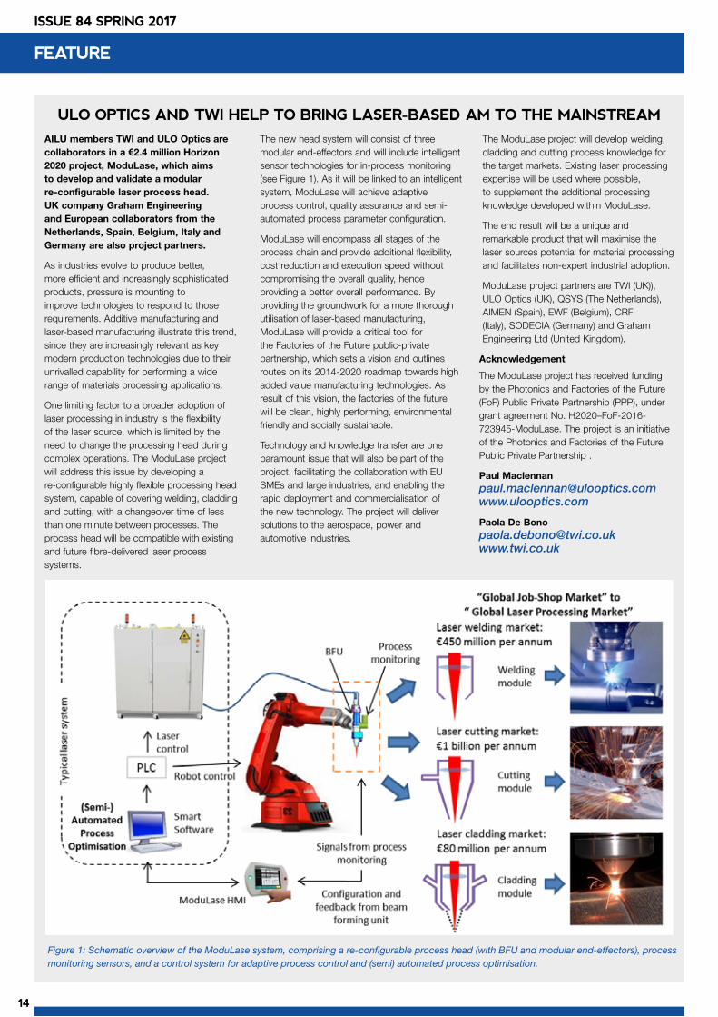
FEATURE
AILU members TWI and ULO Optics are collaborators in a €2.4 million Horizon 2020 project, ModuLase, which aims to develop and validate a modular re-configurable laser process head. UK company Graham Engineering and European collaborators from the Netherlands, Spain, Belgium, Italy and Germany are also project partners.
As industries evolve to produce better, more efficient and increasingly sophisticated products, pressure is mounting to improve technologies to respond to those requirements. Additive manufacturing and laser-based manufacturing illustrate this trend, since they are increasingly relevant as key modern production technologies due to their unrivalled capability for performing a wide range of materials processing applications.
One limiting factor to a broader adoption of laser processing in industry is the flexibility of the laser source, which is limited by the need to change the processing head during complex operations. The ModuLase project will address this issue by developing a re-configurable highly flexible processing head system, capable of covering welding, cladding and cutting, with a changeover time of less than one minute between processes. The process head will be compatible with existing and future fibre-delivered laser process systems.
The new head system will consist of three modular end-effectors and will include intelligent sensor technologies for in-process monitoring (see Figure 1). As it will be linked to an intelligent system, ModuLase will achieve adaptive process control, quality assurance and semi-automated process parameter configuration.
ModuLase will encompass all stages of the process chain and provide additional flexibility, cost reduction and execution speed without compromising the overall quality, hence providing a better overall performance. By providing the groundwork for a more thorough utilisation of laser-based manufacturing, ModuLase will provide a critical tool for the Factories of the Future public-private partnership, which sets a vision and outlines routes on its 2014-2020 roadmap towards high added value manufacturing technologies. As result of this vision, the factories of the future will be clean, highly performing, environmental friendly and socially sustainable.
Technology and knowledge transfer are one paramount issue that will also be part of the project, facilitating the collaboration with EU SMEs and large industries, and enabling the rapid deployment and commercialisation of the new technology. The project will deliver solutions to the aerospace, power and automotive industries.
The ModuLase project will develop welding, cladding and cutting process knowledge for the target markets. Existing laser processing expertise will be used where possible, to supplement the additional processing knowledge developed within ModuLase.
The end result will be a unique and remarkable product that will maximise the laser sources potential for material processing and facilitates non-expert industrial adoption.
ModuLase project partners are TWI (UK)), ULO Optics (UK), QSYS (The Netherlands), AIMEN (Spain), EWF (Belgium), CRF (Italy), SODECIA (Germany) and Graham Engineering Ltd (United Kingdom).
Acknowledgement
The ModuLase project has received funding by the Photonics and Factories of the Future (FoF) Public Private Partnership (PPP), under grant agreement No. H2020–FoF-2016-723945-ModuLase. The project is an initiative of the Photonics and Factories of the Future Public Private Partnership .
Paul [email protected]
Paola De [email protected]
ULO OPTICS AND TWI HELP TO BRING LASER-BASED AM TO THE MAINSTREAM
Figure 1: Schematic overview of the ModuLase system, comprising a re-configurable process head (with BFU and modular end-effectors), process monitoring sensors, and a control system for adaptive process control and (semi) automated process optimisation.

15
ISSUE 84 SPRING 2017
The Welding Engineering and Laser Processing Centre (WELPC) at Cranfield University has established a worldwide reputation in teaching, training, development and innovation in laser processing and additive manufacture.
Our main philosophy is to remove the “black art” from high power laser processes by promoting fundamental understanding of laser material interactions and applying a bottom-up approach to process development.
In this case, the requirements of the material are considered first, and then the process is tailored to meet these requirements. Only then is the suitable laser system specified.
We are a partner in the EPSRC Centre for Innovative Manufacturing in Laser Based Production Processes and lead the fusion based processing theme.
Contact: Wojciech [email protected]
FOCUS ON RESEARCH
HIGH POWER JOINING AND CUTTINGOur main interest in high power joining and cutting is to develop robust and efficient processing by understanding process fundamentals and tailoring the heat of the laser to a particular case.
MICRO JOINING AND PEENINGA large part of our research includes the use of low power CW lasers and nanosecond pulsed lasers for high precision and high productivity processing. The goal is to understand the process requirements and develop cost effective process with consideration of process dynamics and product quality.
Particular areas of interest are:
• Dissimilar metal joining
• Comparison between pulsed and CW processing
• Cost effective laser peening
Fully penetrated fillet joint by laser-arc hybrid welding
ADDITIVE MANUFACTURINGIn this research we are focusing on development of two technologies:
• Near net-shape laser plus wire
• Variable resolution powder bed systems
We are developing processes, which will be able to control microstructural development and mechanical properties of built parts. The spatial and temporal distribution of laser energy is tailored precisely to control the dimensional accuracy of deposits and thermal-cycle. This is applied to wire-based as well as powder bed systems.
PROCESS MONITORING AND SMART PROCESSES We work towards more autonomous and robust processing by applying process understanding and smart monitoring.
Robotic welding of a pipe
Laser marking of a 3D printed titanium part
Dissimilar micro – spot weld
30–layer wall by laser-wire AM
Focus areas are:
• Development of phenomenological models for joining of materials with variable thickness
• Insitu control of thermal-cycle
• High productivity hybrid processes
• Joining of challenging materials
• Dissimilar metal welding
• Process dynamics in cutting
Metal transfer during laser-wire deposition
Signal from process monitor

16
ISSUE 84 SPRING 2017
LASER ENGRAVED MEMORY OF THE GREAT WAR
JOB SHOP CORNER
CIRRUS LASER SPONSORS CRASH TEST STUDENTS
Cirrus Laser has been sponsoring the University of Liverpool Motorsport team for a number of years. The Motorsport team comprises around 30 students who design and build a new single seat race car every year ready to compete internationally at Silverstone. With the help of Cirrus Laser, this year the team has been developing a new impact attenuator which is bolted to the front of the car to mitigate against possible crashes. The impact attenuator must be capable of absorbing 9350 J of energy in a frontal impact.
Cirrus Laser cut all the parts on their new TRUMPF 5030 fibre solid state laser for the construction of both a potential ‘all aluminium’ design and a ‘foam with intrusion plate’ design. Both impact attenuators absorbed the required amount of energy, within the required deceleration parameters. The team have decided to progress with the Foam IA, as this design is easier to manufacture and 1.2 kg lighter than the aluminium design.
Contact: Dave [email protected]
CHARLES DAY TAKES TO THE RACE TRACK
Charles Day recently laser cut several integral parts for Sheffield University’s formula racing team, which were used in the construction of the team’s fastest and most advanced racing car to date. The parts, made from mild steel, stainless and aluminium were used in construction of the chassis (mild steel), chain guard (stainless), fuel tank and wheels (aluminium).
Sheffield Formula Racing represents The University of Sheffield in the Institute of Mechanical Engineers’ (IMechE) annual formula student competition. Each year the team designs, builds and races a single seat formula style race car to take part in a number of events: acceleration, skidpan, sprint and endurance, to test the car’s abilities.
The team consists of students from across the engineering faculty from every year of study and from a wide range of departments – mechanical, aerospace, materials and control systems.
Contact: Jon [email protected]
AILU JOB SHOPS SUPPORT UNIVERITY RACING TEAMS
Charles Day (Steels) and Cirrus Laser are delighted to be involved in the racing sucess of the Universities of Sheffield and Liverpool respectively, as they prepare for the Institute of Mechanical Engineers’ annual formula student competition. Taking place at Silverstone each year, the competition is entered by over 100 universities from around the world.
Lee Simmons is a British artist and designer, specialising in blurred peripheries - bridging the gap between architecture and art-and-design.
Cutting Technologies worked with Lee on his most recent project, The Great War Memorial, a sculpture located on London’s Victoria Street next to Westminster City Hall, designed to commemorate council employees who fought and died during World War 1.
The memorial is made up of 82 shards fabricated from Sicilian carrara marble, which represent each of the employees of Westminster City Council who lost their life.
Cutting Technologies was commissioned to engrave the base of the memorial with the names of the council workers who died during the conflict.
The size of the base required large scale laser engraving and Cutting Technologies were in a positionto tackle such a job. Faced with a short time frame to deliver the project, Lee Simmons and his team were grateful for ther prompt communication, high level of efficiency and quick turnaround speed, which enabled them to meet their tight deadline.
Contact: Martin [email protected]
Images courtesy of Lee Simmonswww.leesimmons.com
17
ISSUE 84 SPRING 2017
Fibre lasers, they are all the rage at the moment. I recently had a conversation with one of the OEMs sales staff who said they think they will stop producing CO2 lasers altogether soon. I’m not 100% convinced myself. Clearly fibre lasers have their niche in the market place. They are undoubtedly fast and give a reasonable cut quality finish for the thin materials, but for materials 4 mm and up I’m yet to see the same quality that you get with a CO2. If you are weighing up the pros and cons of fibre versus CO2, I would like to sound a note of caution. You will have heard that fibre lasers use less electricity, have lower maintenance costs and overall are cheaper to run. But be aware that the electricity saving may not be huge. Whilst fibre lasers do use less electricity, unless you buy a budget-end machine with lower power consumption drive motors, then the only saving comes from the lower energy required for the laser itself. This saving is unlikely to cover the cost of changing your CO2 to a fibre unless you are planning to run it for a long time.
Any saving in electricity may soon be offset by the cost of the nitrogen used. The fibre laser beam width is much smaller, so to compensate, the nitrogen usage is increased by increasing the gas pressure. Also nozzle sizes have increased - remember the area of a circle is the square of the radius, so if the nozzle size doubles you’ll use about 4 times the amount of nitrogen. Even if you have a nitrogen generating plant, bear in mind you still have to pay for all the equipment, maintenance etc. plus the electricity to generate the nitrogen. For thin materials, the nozzle diameters will be similar and your cutting costs will be roughly the same as a CO2, possibly cheaper. On thicker materials costs will increase.
Fibre cutting with almost any material of any thickness will give a slight burr, i.e. the hard, sharp dross material left on the underside of the material. Whilst this is not noticeable on thin materials it is increasingly obvious the
thicker the material. It would be wise to budget for de-burring especially if you are planning to cut thicker materials on your fibre laser.
I have noticed that processing time is key to costing a job, rather than cutting time - the time it takes to load/unload the machine is the same no matter which type of laser you use. Yes, you might cut a whole sheet in 5 minutes that previously took 20 minutes, but if every sheet still takes 20 minutes to load/unload and you start charging your customer ¼ the price, you will soon find yourselves in trouble!
Speaking to other member of the AILU committee many years back we speculated on the maintenance costs of fibre lasers, and we now have a better idea. Discussing this matter again recently, there seems to be a wide range of fibre laser reliability from great to poor. Some companies are experiencing no failures, but others are finding failures are happening much faster than envisaged. One possibility for this could be due to reflections - we were led to believe that reflective materials can be cut on a fibre but now there is some back-tracking. Repair costs are not cheap; whereas a repair to a CO2 is often some thousands of pounds, you must prepare to have fewer but more expensive repair bills, at around £10k+, for a fibre.
As long as you are cutting thin mild, a fibre is perfect; less expensive to run and should be the right choice as long as you quote your prices to include the time for loading/unloading. If you are cutting a variety of materials especially thicker or reflective materials it may be wise to think carefully about potential additional costs.
Mark Millar
CHAIR’S REPORT
LASERLINE® from BOC offers customers the complete package of appropriate gases, customised gas supply solutions and a range of value added technical services.
With supply solutions ranging from bulk liquid through to on-site nitrogen generators, including a range of specialist gas equipment, BOC can offer an impartial view of the most appropriate supply solution to suit your needs.
Talk to someone about your gas requirements or to request your free LASERLINE® technical cutting, welding or additive manufacturing brochure, call BOC on 0800 111 333 or visit
www.BOConline.co.uk/laserline www.BOConline.co.uk/additivemanufacturing
LASERLINE®Leading in laser and additive manufacturing gas supply solutions
Download our Laserline
and additive manufacturing brochures
MY OPINION ON FIBRE VS CO2...
ISSUE 84 SPRING 2017

18
ISSUE 84 SPRING 2017
PRODUCT NEWS
18
INTERVIEW
SELLING PROCESSES - NOT JUST TOOLS AN INTERVIEW WITH ANDY TOMS
DIRECTOR, TLM LASER LTD
Q. Can you give us an overview of TLM Laser?
TLM Laser was formed in 2005, originally as a service provider for UK laser installations. Initially there were 3 staff and the company was registered at my home on the Isle of Wight. Around 5 or 6 years ago we realised that in order to sustain and grow the company we needed to sell systems – at this time we hired Tony Dain and purchased an office near Bromsgrove out of our
pensions, which seemed like an excellent funding model.
The company grew significantly, and 11 years on, now employs 11 people and turns over around £2.5 million with a growth target of 20-25% per year. Initially we represented FOBA for laser marking systems, adding other German suppliers; Alpha for laser welding of metals and LPKF for plastic welding. We also
have laser cutting systems from Coherent and Swisstek and Additive Manufacturing from InssTek of South Korea.
We maintain virtually all of the WaferMark business in the UK and Ireland, installing and maintaining used systems or supplying new systems from InnoLas for the semiconductor industry. We also supply laser safety eyewear from Univet in Italy, and BOFA fume extraction.
INTERVIEW

19
ISSUE 84 SPRING 2017
INTERVIEW
Q. What makes TLM different from your competitors?
We have cherry-picked the expert suppliers of systems from around the world in each market sector to be able to offer solutions which are both technically advanced and extremely reliable. Re-badging other peoples’ systems is not a road we would consider going down. We sell applications and processes not machines, focusing on the best solution rather than the product itself. This strategy has allowed us to secure repeat business from existing customers, some of whom have several systems from different manufacturers supplied and maintained by TLM. We generate most of our business from online marketing, trade shows and advertising - our website is very well optimised, and we recognised the importance of SEO a long time ago.
Q. Do you offer a sub-contract service as well as systems sales and service?
No, we believe that offering both would set us up in competition with our customers. Our clients often earn their living from outsourced laser processing, and they wouldn’t appreciate us competing in their market. Instead we concentrate on providing systems and after-sales service. We have a well-equipped demo area where we like to allow our clients some time to get to know the equipment and we find that when they become familiar with the operation of our welding and marking systems they can appreciate the benefits and we find that puts us ahead of the competition.
Q. What do you think about the political situation in the UK at the moment?
During the last four years we have had a major political upheaval each year; the Scottish Independence Referendum in 2014, the General Election in 2015, the Brexit Referendum in 2016 and now another General Election in 2017. Such events can create some uncertainty which can disrupt the buying decision timing – but I suspect that sometimes our clients use this as an excuse when they have actually decided that they aren’t going to proceed with a capital purchase.
Successive UK governments have failed to give manufacturing industry the importance and priority it deserves and we recognise the skills shortage which we can trace back to the lack of structured industrial training and apprenticeships over the past few decades. The lack of skilled and experienced toolmakers under 50, for example, is a significant problem – drawing in qualified engineers and toolmakers from Eastern Europe is filling a gap but highlights a weakness in the education and training in the UK.
Q. What would you like to see more of?
I feel the UK would benefit from more people who are willing to invest and take risks. Remembering the late Maurice Gates, he was willing to take risks and invest in the latest technology to build a business from nothing – and now Micrometric is one of the leading precision sub-contractors and that sector has grown significantly. In other areas like plastic welding, cladding and hardening, the UK is lagging perhaps 5 to 10 years behind Germany in the adoption of these technologies.
Q. What are the key markets for TLM?
We have a strong position in semiconductor and wafer marking, though that business has declined in the UK in recent times. Medical, automotive and aerospace are strong for us and we have a very good relationship with the tool and die industry, especially for welding and engraving systems. Our approach to offering systems with ease of use and high quality with helpful functions like TTL vision on our laser marking systems and smooth joystick control and ergonomics on the welding systems means that we are not targeting the people who are looking for the “bargain basement” equipment.
Q. How important is AILU membership to you?
We have been AILU members since the beginning of the company, and in my previous role we joined AILU when it started. As a body that promotes the use of lasers and is involved in lobbying politically, we feel it is a very important “umbrella organisation” in particular for the UK. Recently a potential client asked, “Are you a member of AILU?” so the AILU brand is gaining recognition and significance year on year and also becoming known outside the UK, for example in USA.
Contact: Andy [email protected]
Re-badging other peoples’ systems is not a road we
would consider going down
“
”
Recently a potential client asked, “Are you a
member of AILU?”
“
”

20
ISSUE 84 SPRING 2017
WELDING
NUCLEAR WELDING: POTENTIAL
AND CHALLENGES FOR LASERSNEIL IRVINE & JOHN FRANCISIn recent years there have been calls to revisit the options that are available for the welding of safety-critical nuclear pressure vessels, such as those that are employed in light water reactors. The desire to look again at joining technologies stems from renewed interest in nuclear new build, following a period of slowdown that was initially triggered by the Three Mile Island accident (USA) in 1979 and compounded by the Chernobyl disaster (USSR) in 1986.
In the three decades following the Three Mile Island accident new reactor construction in the western world, and particularly in the USA, fell back and the economic incentives for making a case to change engineering codes did not exist. Accordingly, fabrication standards overseen by professional associations such as the American Society for Mechanical Engineers (ASME) have restricted the choice of welding processes that are approved for use in the fabrication of critical nuclear components.
A schematic representation of the major components in a pressurised water reactor (PWR) is shown in Figure 1, with component diameters and wall thicknesses given in Table 1. The pressure vessels are usually manufactured from a low-alloy steel while the pipes are generally manufactured from an austenitic stainless steel. Vessels and pipes such as these are currently welded using arc-based technologies such as submerged-arc welding (SAW) and gas-tungsten arc welding (GTAW).
Given the dimensions and wall thicknesses that apply, individual welds often require in the order of 100 weld passes and can take several weeks to complete.
In recent years, some attention has been paid to the possibility of applying electron beam welding to the manufacture of large nuclear vessels [2]. Owing to the difficulties associated with placing such large vessels into a vacuum chamber, attention has focused on welding under reduced pressures (instead of welding under a high vacuum), and the use of local sealing systems. The potential for making such thick welds in a single pass is clearly attractive from both economic and production standpoints. However, there are hurdles to be cleared before the reduced pressure electron beam (RPEB) welding process can be applied in practice. It should also be noted that the differences between an arc weld process involving ~100 weld passes, with interpass tempering effects, and a single pass keyhole mode weld are considerable.
Multipass narrow gap laser welding
Within the framework of the New Nuclear Manufacturing research programme (NNUMAN), researchers have explored an approach that is intermediate between arc welding and a single pass electron beam weld, using multipass narrow-gap laser welding (NGLW) to make welds in thick sections of steel. Initial trials focused on making such a weld in 30 mm thick test pieces of SA508 Grade 3, Class 1 steel, typically used in the manufacture of reactor pressure vessels. The motivation for using this approach stemmed from:-
• a desire to explore the potential for applying lasers in the manufacture of nuclear components,
• the idea that, by using a narrower weld groove, the weld would still benefit from pass-to-pass tempering effects while dramatically reducing the volume of weld metal that needed to be deposited.
A schematic representation of the welding set-up is given in Figure 2. An ytterbium fibre laser was used, with a maximum available power of 16 kW. The beam parameter product was 10 mm.mrad, and the minimum spot diameter was 0.8 mm. A filler wire with a diameter of 1.2 mm was used. Results from some of the earliest welding trials [3] are shown in Figure 3. The objective during these trials was to identify welding parameters that could be used to complete the root pass in keyhole mode in order to reduce the number of filling passes that was required. However, it became apparent that the aspect (depth/width) ratio of the weld bead played a critical role in the avoidance of cracking on cooling. Lower values for the aspect ratio were found to be more resistant to cracking. For this reason, the complete weld was made in conduction mode using a defocused beam. Vertical sidewalls were employed, with an initial groove gap in the order of 4 – 5 mm. The use of a defocused beam assisted in achieving adequate sidewall fusion.
A macrograph from a successful welding trial in a 30 mm thick low-alloy steel is shown in Figure 4, while the corresponding (Vickers) hardness maps for a similar weld in SA508 Grade 3 Class 1 steel are shown in Figure 5, both in the as-welded condition and after post-weld heat treatment (PWHT). The feasibility of manufacturing welds at this thickness using multipass NGLW was demonstrated, without cracking or lack of sidewall fusion. Successful welds typically involved making an autogenous root pass, followed by 6-9 filling passes. The hardness maps in Figure 5 reveal that there are noticeable pass-to-pass tempering effects when using multipass NGLW, since the hardness in the vicinity of the last weld pass is noticeably higher than it is within weld metal corresponding
Figure 1: Schematic representation of the primary circuit in a pressurised water reactor, showing the reactor pressure vessel (red), the steam generators (purple/black) and the pressuriser (blue), after Xing et al. (2017) [1]
Figure 2: Schematic representation of the welding set-up for multipass NGLW of low-alloy steels, showing the delivery of filler wire ahead of the beam, with a trailing argon gas shroud, after Feng et al. [3]
Diameter Wall thickness
Reactor pressure vessel (red)
3-5 m 200-250 mm
Steam Generators (purple/black)
~5 m 100-150 mm
Pressuriser (blue) ~2 m 100 mm
Interconnecting pipes 0.8 – 1.0 m 80 mm
Table 1: Representative PWR component diameters and wall thicknesses

21
ISSUE 84 SPRING 2017
to previously deposited weld beads. The hardness results for the weld after PWHT reveal that the weld has responded well to a standard PWHT procedure for this steel. Indeed, all of the indicators suggest that, from a material property standpoint, multipass NGLW produces sound welds.
Challenges
The principle challenges that confront multipass NGLW relate to process reliability, a vital consideration when dealing with costly safety-critical components. Lack of sidewall fusion cannot be tolerated in the nuclear sector, and it proved to be particularly problematic during the developmental trials. However, when consideration is given to typical spot sizes for lasers and the need to bridge a weld groove gap with a width in the order of 5 mm, when the groove walls are vertical (or near to it), it soon becomes apparent that melting of the groove walls is likely to be problematic.
It is difficult to see a way around this problem for very thick joints. On the one hand, if the width of the weld groove is reduced, it becomes very difficult to maintain adequate shielding gas coverage at the bottom of the groove, and to maintain reliable delivery of the filler material. On the other hand, if a bevel is introduced to the groove walls, the width of the
weld groove becomes too large to bridge as the joint thickness increases. Problems were also encountered with porosity, owing to the difficulties associated with shielding in narrow and deep grooves.
Overall, the productivity gains that should have materialised from a smaller weld groove were offset by the higher deposition rates that can be achieved with processes such as submerged arc welding. Finally, and perhaps very significantly, the laboratory trials involved relatively small-scale test pieces that were very well aligned. It is difficult to imagine a scenario in which adequate joint fit-up (for the purposes of laser welding) is achieved around the circumference of components in excess of 3 m in diameter.
Potential for alternative approaches
While work on the development of laser-based strategies for the joining of thick components is ongoing, alternative technologies are also advancing. There is a distinct possibility that reduced pressure electron beam welding will be approved for the manufacture of safety-critical nuclear components in the next 5 years. With this in mind, proponents of laser welding should aspire to achieve a competitive advantage over electron beam welding, rather than over arc welding processes.
In recent years, developmental work has begun on vacuum (or reduced pressure) laser welding. The early indications are that, when using the same beam power and welding speed, reduced pressure laser welding can match the penetration capabilities of an electron beam, with less onerous shielding requirements (no X-rays are generated), and laser-based approaches are not susceptible to deflection of the beam when a steel has been magnetised to some degree. The challenges associated with alignment that arise in multipass NGLW will be mitigated to
some degree by opting for a square-butt joint configuration, and the issues with deposition rate become irrelevant when an autogenous weld is employed. At present, the principal limitation on the penetration that can be achieved with vacuum laser welding is the beam power. However, one can certainly imagine that available laser powers will increase in the years ahead.
Concluding remarks
The case for applying lasers to the welding of very large nuclear components with thicknesses exceeding 50 mm is not obvious, especially in the case of multipass narrow-gap laser welding. In comparison to alternative technologies, laser welding utilises a narrower weld groove, and it requires a degree of alignment that is currently not feasible when dealing with the large components that arise in the nuclear sector. In the longer term, the most likely competitor to laser welding is likely to be reduced pressure electron beam welding, which offers a step change in productivity over arc welding processes. The most promising option for the application of lasers is therefore likely to be vacuum laser welding, which has the significant advantage of being insensitive to residual magnetism within steels, which becomes an important consideration when the joint thickness becomes large.
References
[1] J. Xing, D. Song, Y. Wu “HPR1000: Advanced Pressurized Water Reactor with Active and Passive Safety”, Engineering, 2 (1), 2016, 79-87
[2] K. R. Ayres, et al. Paper PVP2010-25957, Proceedings of the ASME 2010 Pressure Vessels and Piping Division Conference, Bellevue, Washington, USA, July 18–22, 2010
[3] J. C. Feng et al. International Journal of Advanced Manufacturing Technology, 88 (5-8), pp. 1821-1830, 2017.DOI: 10.1007/s00170-016-8929-1
Acknowledgement
The authors gratefully acknowledge financial support provided by the Engineering and Physical Sciences Research Council through the NNUMAN programme grant in nuclear manufacturing (Grant number: EP/J021172/1).
Neil Irvine: Dalton Nuclear Institute,John Francis: School of Mechanical, Aerospace & Civil Engineering, both The University of Manchester
Contact: Neil [email protected]
Neil Irvine is Program Manager of the EPSRC funded New Nuclear Manufacturing (NNUMAN) programme at The University of Manchester and Chair, Research Board, Nuclear AMRC.
SEE OBSERVATIONS P32
WELDING
Figure 3: Results of preliminary welding parameter trials showing the tendency for cracking, particularly in weld beads with a high depth/width ratio, adapted from Feng et al. [3]
Figure 4: Macrograph from a successful weld in a 30 mm thick pressure vessel steel. An autogenous root pass in combination with 6-9 filling passes worked best (after Feng et al. [3]).
Figure 5: Maps of Vickers hardness for successful welds in 30 mm thick SA508 Gr. 3 Cl. 1 steel using multipass NGLW, in the as-welded condition (left) and after PWHT (right).

22
ISSUE 84 SPRING 2017
22
LASER POLISHING
LASER POLISHING: A FLEXIBLE
APPROACH FOR SMOOTHING SURFACES WOJCIECH GORA Additive manufacturing (AM) is making a strong push into many industrial sectors, such as medical, aerospace, defence. The main driving factor behind this is that AM is a design driven technique of manufacturing elements that is much less constrained than traditional manufacturing techniques. As a result AM parts can have improved properties, allow new applications and functions and require less material as opposed to those manufactured using traditional subtractive manufacturing techniques. However, AM parts typically have somewhat rough surfaces and hence require post processing, dependent on the targeted application e.g. when considering biological implants the surface has to be smooth enough to prevent damage to the adjacent tissue as well as to limit potential bacteria growth on the contact surface between the element and tissue.
Currently there are two main techniques used in polishing of AM parts: electrochemical and mechanical polishing. Unfortunately both of these techniques have their limitations. Electrochemical polishing is not a very selective process and requires further processing or additional masking when there is a requirement for different grades of surface finish required on the same part for functional purposes. On the other hand mechanical processing struggles when dealing with free form surfaces. Laser polishing meanwhile offers an intriguing option; it is a process that can be automated, is highly repeatable, has a short process duration, is capable of selective polishing of microscale areas and is more environmentally friendly as it does not use an abrasive or liquids.
Unlike mechanical or electrochemical polishing, laser based polishing in not a subtractive technique, instead the laser energy is used to melt the surface, which then flows under surface tension. The laser beam is scanned across the surface in order to create a thin layer of molten material. Various different scanning strategies and parameters can be appropriate, dependent on the material used, the desired surface finish and the initial surface state. Laser polishing is normally split into two regimes: macro – using continuous wave (CW) laser and micro – using a short pulsed laser (Figure 1).
The major difference between the modes of laser polishing is the melt depth which ranges from 5 to 200 µm for macro laser polishing and
1 to 5 µm for micro laser polishing [1]. As a result macro laser polishing is better suited for the removal of larger scale structures as it has a larger melt depth. For micro laser polishing to be effective the size of structures on the surface has to be smaller due to the significantly lower melting depth of the process. As a result both macro and micro laser polishing are often used one after another to achieve best final effect.
Laser based smoothing does have its limitations. The initial surface shape, texture and feature size influence the final state of the polished surface. If the wrong parameters are selected it is possible to create various unwanted structures, for example ripples, undercuts, bulges, step structures and martensite needles [2]. Moreover with laser polishing it is not possible to achieve a completely flat surface, instead a waviness is always present. That is due do the capillary forces at the boundary between different phase of the material – solid and molten. The effect of this waviness can be clearly seen in Figure 2 where the tip of the pen has a sharp reflection whilst further away the reflection is blurred.
The two main applications that we are currently focused on are connected with bespoke biomedical applications – dental and cranial
implants (Figure 3). Custom dental implants are made from cobalt chrome using selective laser melting (SLM). This powder-based process generates a rough surface and so electrochemical polishing is used following the build process. The bottom part of the implant that sits in the gum must be smooth to prevent any damage to the adjacent tissue and to prevent bacteria growth at the site where the implant is placed. On the other hand the top of the implant requires a somewhat rough surface to provide a strong bond to the crown that will be cemented onto the implant. Unfortunately electrochemical polishing is not a sufficiently selective enough process and further processing is typically required to re-introduce a rough surface to this region. Hence laser polishing is a very attractive solution as it is a spatially-selective process. Cranial implants are also manufactured using SLM, in this case from a titanium alloy - Ti6Al4V. After the part is built it normally requires many different steps of mechanical polishing, which is time consuming and complicated. Laser polishing offers the prospect of significantly reducing the post-processing time, whilst also being a process that is much easier to automate.
Our work was focused on finding processing parameters that are best suited for laser smoothing of the surface of the SLM AM
Figure 1: The difference between polishing with continuous laser radiation (macro polishing) and pulsed laser radiation (micro polishing). Image adapted from Temmler et al. [1]
Figure 2: Laser polished stainless steel showing the effect of waviness (Source: Heriot Watt University)
Figure 3 (a, b) Cobalt chrome bespoke dental implants. (c) Bespoke Ti6Al4V cranial implant (Source: Renishaw)
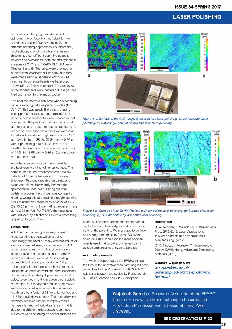
23
ISSUE 84 SPRING 2017
parts without changing their shape and achieving the surface finish sufficient for the specific application. We have tested various different scanning approaches (uni-directional, bi-directional, changing angles of scanning directions, etc.), different scanning speeds, powers and overlaps on both flat and cylindrical surfaces of CoCr and Ti6Al4V SLM AM parts (Figures 4 and 5). The parts were provided by our industrial collaborator Renishaw and they were made using a Renishaw AM250 SLM machine. In our experiments we have used 100W SP-100C fibre laser from SPI Lasers. All of the experiments were carried out in a gas cell filled with argon to prevent oxidation.
The best results were achieved when a scanning pattern imitating halftone printing angles (18°, 72°, 0°, 45°) was used. The benefit of using this approach instead of e.g. a simple raster pattern, is that consecutive laser passes do not overlap with the previous ones and as a result do not increase the size of bulges created by the preceding laser pass. As a result we were able to reduce the surface roughness) of a flat CoCr part by a factor of 38 (Sa 22.84 µm → 0.60 µm with a processing rate of 0.33 mm2/s. For Ti6Al4V the roughness was reduced by a factor of 21.5 (Sa 18.58 µm → 0.86 µm) at a process rate of 0.5 mm2/s.
A similar scanning approach also provided the best results on the cylindrical surface. The sample used in the experiment was a hollow cylinder of 15 mm diameter and 1 mm wall thickness. This was mounted on a rotational stage and placed horizontally beneath the galvanometer scan head. During the laser polishing process the cylinder was constantly rotating. Using this approach the roughness of a CoCr cylinder was reduced by a factor of 11.5 (Sa 13.05 µm → 1.12 µm) with a processing rate up to 0.33 mm2/s. For Ti6Al4V the roughness was reduced by a factor of 10 with a processing rate of up to 0.5 mm2/s.
Conclusions
Additive manufacturing is a design driven manufacturing process which is being increasingly exploited by many different industrial sectors. In almost every case the as-built AM parts require some form of post processing before they can be used in a final assembly or as a standalone element. An interesting approach to the post processing of AM parts is laser polishing that does not have the same limitations as more conventional electrochemical or mechanical polishing. It provides a spatially-selective surface finishing process that is quick, repeatable, and readily automated. In our work we have demonstrated a reduction of surface roughness by a factor of 38 for a flat surface and 11.5 for a cylindrical surface. The main difference between achieved factors of improvements between flat and cylindrical surfaces is mainly due to the different initial surface roughness. Moreover when polishing cylindrical surfaces the
beam was scanned across the sample which led to the beam being slightly out of focus for parts of the polishing. We managed to achieve processing rates of up to 0.5 mm2/s, which could be further increased if a more powerful laser is used that would allow faster scanning speeds and larger spot sizes to be used.
Acknowledgements
This work is supported by the EPSRC through the Centre for Innovative Manufacturing in Laser-based Production Processes (EP/K030884/1). Additional support is provided by Renishaw plc, SPI Lasers, Alicona and GKN Aerospace.
References
[1] A. Temmler, E. Willenborg, K. Wissenbach, Proc. SPIE 8243, Laser Applications in Microelectronic and Optoelectronic Manufacturing (2012).
[2] C. Nusser, J. Kumstel, T. Kiedrowski, A. Diatlov, E.Willenborg, Advanced Engineering Materials (2015).
Contact: Wojciech Gora
Wojciech Gora is a Research Associate at the EPSRC Centre for Innovative Manufacturing in Laser-based Production Processes and is based at Heriot-Watt University.
SEE OBSERVATIONS P 32
LASER POLISHING
Figure 4 (a) Surface of the CoCr angle bracket before laser polishing. (b) Surface after laser polishing. (c) CoCr angle bracket before and after laser polishing.
Figure 5 (a) Surface of the Ti6Al4V hollow cylinder before laser polishing. (b) Surface after laser polishing. (c) Ti6Al4V hollow cylinder after laser polishing.

24
ISSUE 84 SPRING 2017
The generation of Laser Induced Periodic Surface Structures (LIPSS) using ultrashort-pulse laser irradiation is a flexible method to texture surfaces. For industrial applications, the ability to process surface areas at a speed compatible with commercial requirements is critical for economic viability. Traditional methods for controlling LIPSS generation involve selecting a set of process parameters such as the wavelength and pulse energy to achieve either a good uniformity or the highest possible scanning speed. Controlling the process through unconventional methods such as polarisation or wavefront shaping allows optimisation of both uniformity and scan speed resulting in much greater flexibility in the range of potential applications.
Laser Induced Periodic Surface Structures (LIPSS) are a general phenomenon observed after irradiation of various surfaces with short or ultrashort-laser pulses (Figure 1). These structures have gained significant interest in recent years, since it was demonstrated they can be produced with periods well below the wavelength of the incident laser using femtosecond irradiation. LIPSS textured surfaces have been shown to develop novel optical, mechanical or chemical properties [1] and are easily produced. Therefore LIPSS-based texturing processes have a wide range of potential applications and compare favourably to traditional methods such as lithography [1].
A surface textured with LIPSS can diffract white light very effectively, which gives the appearance of bright colours. This can be used for colour coding, decoration and customised products: this was demonstrated with the reproduction of artistic images onto the surface of metals such as stainless steel, where the different colours are achieved due to varying the orientation of the LIPSS. By viewing under a certain angle the colours appeared similar to the initial image. Similarly, LIPSS can be used as an anti-counterfeiting alternative to security labels. Furthermore, LIPSS texturing can lead to a significant reduction in reflectivity and can enhance the absorption of light by the material. A combination of macro-, micro- and nanostructures on the surface can lead to almost 100% absorption and make the surface appear black. The durability of these patterns is high in comparison to porous silicon produced by chemical etching that can easily be damaged [2].
Another promising area is the control of wettability, which is key in a wide range of applications such as microfluidics, biomedicine, fuel cells and catalysts chemicals. LIPSS are also reported to influence the contact angle of laser-structured surfaces creating hydrophobic as well as hydrophilic areas. A combination of micro, macro and nanostructures can result in a highly anisotropic response that has been shown to allow metal surfaces to pump liquid uphill.
In all these examples the most critical factor for industrial scalability is the control of process parameters to achieve high uniformity, reliability and speed. Current laser-based processes typically only consider process control
parameters such as wavelength, pulse-length, pulse energy, repetition rate and scan speed; however, the polarisation and intensity profile of the incident beam also have a major influence on the formation process of LIPSS and thus the quality of the resultant product and yet they are not considered in existing processes [3].
In a recent research project, the author and Dr Walter Perrie from the Laser Group at the University of Liverpool have shown the benefits of controlling the polarisation and intensity profile for the generation of LIPSS on different types of substrates: polished stainless steel, copper, and indium tin oxide (ITO) thin film on glass. To produce uniform LIPSS on a given surface area, a range of laser processing parameters has to be found and this is very sensitive to the type of target material. For steels, the fluence needs to be somewhat higher than the ablation threshold, which is around 0.2 J/cm2 for single pulse irradiation and 0.1 J/cm2 for 100 pulses at 775 nm wavelength, with a 150 fs pulse laser. For texturing metals with a high thermal conductivity like copper (ablation threshold ~0.35 J/cm2) the laser-processing window tends to be fairly narrow, and this often results in a comparatively slow scan speed. Texturing LIPSS on thin films such as ITO requires identifying a very fine processing window, since the laser fluence needs to be just below the ablation threshold to prevent removal of the film, but above the modification threshold, which is around 0.3J/cm2 for femtosecond irradiation at the chosen wavelength. This can be achieved by making use of incubation effects were multiple pulses are applied below the ablation threshold.
Once suitable laser texturing parameters have been identified, the specific geometry of LIPSS patterns required to produce the surface image has to be taken into account. This can be achieved in a very flexible way by using dynamic control of polarisation and intensity profiles of the laser beam. The results are scalable allowing the optimisation and control of large areas for structuring.
Figure 2 shows the feasibility of generating LIPSS using dynamic, real-time polarisation control where a liquid-crystal polarisation rotation device is synchronised to the scanning galvanometer during laser processing. This method is very flexible and enables full control of the polarisation direction over the whole surface area. This allows any periodic pattern of colours, with a speed of up to 20 kHz, determined by the maximum rotation speed of the liquid-crystal
IMPROVED SURFACE TEXTURING
FOR INDUSTRIAL APPLICATIONS OLIVIER ALLEGRE ET AL.*
Figure 1: LIPSS textured on the surface of (a) polished stainless steel using a 10 ps pulse-length, 532 nm wavelength and 1.8 J/cm2 fluence; (b) titanium using 10 ps pulse-length, 1064 nm and 0.4 J/cm2 fluence. The red arrow indicates the direction of the incident linear polarisation
SURFACE TEXTURING
5μm
1μm
a b

25
ISSUE 84 SPRING 2017
waveplate to be produced. Experiments have shown that the minimum periodicity of LIPSS rotation allows images with a feature size below 20 μm to be created.
Figure 3 shows an alternative approach where the polarisation was controlled by mechanically rotating a waveplate during processing, altering the LIPSS growth angle to achieve various colours. Although this approach only permits a much slower rotation speed, the range of rotation angle is greater allowing for more complex patterns to be created.
One such example of a complex pattern using spatially variant polarisation modes is presented in Figure 4. This example used a
combination of radial and azimuthal polarization to produce spirally shaped LIPSS patterns [4]. Surface texturing can also be optimized by shaping the beam wavefronts using light control devices such as Spatial Light Modulators (SLM) or Diffractive Optics (DO). In Figure 5a, a Fresnel function is used to de-focus the beam, allowing to expand the ablation spot diameter and thus helping to increase the processing speed by reducing the number of scanned lines. An interesting alternative is to use an annular beam, which can be produced with a so-called vortex function, as shown in Figures 5b and 5c.
Conclusions
The formation of LIPSS is a convenient method to texture surfaces with sub-micrometer features over large areas. However producing LIPSS requires achieving a tight control over the laser process parameters and this often affects processing speed and quality. Novel experimental methods have become available to shape the laser beam polarisation and wavefronts and this greatly enhances the process control. It has been shown that these methods can be used to quickly produce complex patterns with a very high spatial resolution. These methods open new avenues in high speed and/or large area LIPSS patterning for example in industries using surface texturing of metals, dielectrics or semiconductors. Such applications include encoding serial numbers on steel or copper parts, or the periodic structuring of transparent thin conducting films for enhancing the efficiency of solar cells.
References
[1] Ran, Lingling; Guo, Zhongyi; Qu Shiliang. Applied Physics A 100 (2010), p. 517-521
[2] Vorobyev, A.Y.; Guo, C. Optics Express 19 (2011), Issue S5, p. A1031-A1036
[3] Y. Jin, O. Allegre, W. Perrie, G. Dearden. Optics Express 21 (21), 25333-43, 2013
[4] O. Allegre, Y. Jin, W. Perrie, G. Dearden. Optics Express 21 (18), 21198-207, 2013
* Olivier Allegre, Linda Pabst, Walter Perrie, Stuart Edwardson, Geoff Dearden
Olivier Allegre: Laser Processing Research Centre, University of ManchesterLinda Pabst: Hochschule Mittweida, GermanyWalter Perrie, Stuart Edwardson, Geoff Dearden: The Laser Group, University of Liverpool
Contact: Olivier [email protected]
Olivier Allegre lecturers at the Laser Processing Research Centre, University of Manchester. He specialises in advanced laser processes, with a special interest in ultrashort-pulse laser material interactions.
SEE OBSERVATIONS P32
Figure 2: Surfaces textured with LIPSS by rotation of polarisation using a dynamic liquid-crystal waveplate: on copper (a) & (b) and 100 μm indium tin oxide film on glass (c) & (d)
Figure 3: Image imprinted on a stainless steel surface, using various orientations of LIPSS to achieve a colour effect
Figure 4: Ablation spot produced on a stainless steel surface, using spatial shaping of the polarisation, with 10 ps pulse-length at 532 nm
Figure 5: Fresnel function (a) and vortex function (b) which are used to shape the wavefront of the beam and optimize its intensity profile. In the example shown in (c) a vortex function is used to produce an annular profile
SURFACE TEXTURING
1 mm 1 mm
a b
c
d a
b
c

26
ISSUE 84 SPRING 2017
Within the last few years, tremendous progress has been achieved in the development of ultrafast laser sources with high average-power (>100 W) in the sub-picosecond regime. Such systems permit ultra high precision laser microprocessing of industrial materials including transparent substrates. Several advanced applications have benefited already including in photonics, microelectronics, MEMS, refractive eye (LASIK) surgery, security marking for anticounterfeiting, biomedical device manufacturing, etc.
Material removal using laser pulse lengths in the range 5 fs to 20 ps is unlike conventional nanosecond or longer pulsed laser ablation. The main differences are as follows:
• Very high peak laser intensities greater than 1014 W/cm2 can be achieved with focused light, powerful enough to ionise any material.
• Non-linear light absorption enables ablation of virtually any material, even transparent materials with a wide bandgap above the incident photon energy.
• The strong absorption nonlinearity can restrict ablated feature sizes to sub-diffraction levels, if a narrow region in the focused spot centre only exceeds the optical breakdown threshold.
• The highly deterministic ablation behaviour below a few ps decouples ablation from stochastic thermal processes, ensuring limited thermal load on a substrate and has important implications on overall resulting feature quality and reproducibility.
• The hydrodynamic motion of the emerging ablated matter and associated complexities for material removal can be ignored, i.e. no laser-plasma interactions are involved above the illuminated surface that typically result in beam attenuation for nanosecond or longer ablation by absorbing/scattering part of the incoming laser beam.
Maintaining very high laser intensities on target, typically above 1012 W/cm2, is often key in several such applications. This can be achieved by either high laser pulse energies or very short laser pulses given a nominal spot size. Laser pulse energies of several millijoules are already commercially available but only at output frequencies of few kHz. Such low frequencies limit effective laser process speed and so negate any competitive advantage gains from ultrahigh precision. Similarly, most industrial femtosecond
laser systems are based on Yb-doped crystals, which, although capable of reliably generating “industrial grade” ultrafast pulses, are usually in the order of few hundred femtoseconds duration. It is therefore desirable to build a new femtosecond laser source capable of both the highest output pulse energy and the shortest sub-100 fs pulse duration possible emitted at the highest feasible laser frequency, in order to satisfy both requirements for high laser intensity on target and high throughput potential.
A consortium of leading European organisations have joined forces under Framework Seven EU project TiSa TD (2013-2017) intending to achieve just that by exploiting three key technologies:
• Ti:sapphire laser technology
• Thin disc laser architecture
• Diamond based crystal cooling
The main objective of the TiSa TD project is to increase the average output power available to at least 200 W whilst keeping the pulse duration below 100 fs by using Ti:sapphire as laser active material in thin-disk geometry and to address high pulse energies as well as high repetition rates. Using a high-power mode-locked oscillator, a pulse energy of 20 µJ is aimed at a repetition rate of about 10 MHz.Pulse energies of up to 10 mJ at 20 kHz is achieved using a multipass amplifier scheme.To achieve this without cryogenic cooling, an improved symmetrical cooling of the laser crystal is required using low-loss transparent diamond heat spreaders as shown in Figure 1.
The consortium partners and their roles are as follows:
• Institut für Strahlwerkzeuge (IFSW), University of Stuttgart (coordinator, development of high-power mode-locked Ti:sapphire thin-disk oscillator);
• Thales Optronique SA (development of high power Ti:sapphire thin-disk amplifier);
• Element Six (synthetic diamond materials development);
• Oxford Lasers (laser applications development with MHz Ti:sapphire fs laser oscillator, market exploitation),
• CNRS FEMTO ST (laser applications development with fs laser amplifier),
• M-Squared lasers (pre-prototype TiSa laser oscillator system including electronics interfacing),
• Kite Innovation (project management and exploitation support).
Several achievements have been reached by all partners during the course of the project. Due to space limitations will be discussing only few of those below.
Ti:sapphire crystals, Quetschi laser concept and diamond crystal cooling
Titanium3+ doped sapphire (Ti:Sa) is the most suitable laser crystal to reach short sub-100 fs pulse durations due to its extremely broad emission bandwidth. Ti:Sa is capable of producing ten times shorter pulse durations than otherwise using Yb-doped crystals. But so far, due to the lack of powerful, cost-efficient pump sources in the blue-green spectral range, Ti:Sa laser systems come at average output powers well below 100 W. Additionally, despite the excellent thermal conductivity of sapphire, thermal lensing effects inside a normal end-pumped Ti:Sa rod limit its dynamically stable fundamental mode of operation to less than about 10 W per crystal at room temperature. To get around this problem, some current high-power Ti:Sa laser systems must be cryogenically cooled. This increases their size and complexity making them unattractive for most industrial
PRECISION MICROPROCESSING
PRECISION MICROPROCESSING WITH
HIGH POWER, ULTRAFAST LASERS DIMITRIS KARNAKIS
Figure 1: Quetschi laser architecture concept developed by IFSW Univ. Stuttgart with two sided diamond based cooling of thin disc laser gain geometry in a transmissive configuration, (right) gain module details. Image copyright University of Stuttgart
Conventional thin disc laser
TiSa TD new improved thin disc laser

27
ISSUE 84 SPRING 2017
PRECISION MICROPROCESSING
applications. To achieve dynamically stable high-power operation without cryogenic cooling, we use thin-disk geometry instead of the commonly used rod geometry.
The lack of cryogenic cooling allows for a significantly more compact laser design. To address the high heat generation of Ti:Sa during high power pumping (about four times higher than Yb:YAG), IFSW implemented a transparent pump module configuration (“Quetschi” concept) with an improved cooling concept: symmetrical double-sided intracavity cooling of the pump module using two transparent diamond heat spreaders that cool the laser crystal from both sides. Based on this Ti:Sa thin-disk gain module, the two laser systems (multipass CPA-system and high-power oscillator) are developed.
Diamond is an excellent material for high power laser applications due to its exceptional optical, thermal and mechanical properties. Natural diamond is not usually considered due to property variability, limited availability and cost of suitably sized crystals. However CVD synthetic diamonds are affordable and especially suited to optical applications exhibiting very low birefringence and optical absorption due to good control of nitrogen related defects. The specific challenge for the TiSa TD project relates to growing enough diamonds of a sufficiently high quality at high yield and polishing them to prepare low roughness “optical” finish diamond for good optical contacting.
Element Six has managed to synthesise optical quality single crystal diamond with diameter of >8 mm. By careful control of the impurity concentrations in the material, the optical absorption was reduced to less than 0.005 cm-1 at 1064 nm. Matched pairs of 8 mm diameter round intracavity heat-spreader components were manufactured and specially polished to achieve a radius of curvature of 5 m on one side of the crystal disc. Additionally, pairs of polycrystalline diamond rings were manufactured to act as high thermal conductivity mounts for the single crystal diamond heat-spreaders.
Laser Applications Development
CNRS FEMTO-ST has investigated micro-nanoprocessing of sapphire crystals with high aspect ratio Bessel beams formed from an ultrafast Ti:Sa laser. They showed that a single femtosecond laser pulse with sufficient laser intensity is capable of opening a sub-µm void in the bulk of sapphire with ultra-high aspect ratio of more than 100:1. It is believed that micro-explosions within the bulk are created with such high generated pressure that they can compress the material around the fabricated nanochannel (several 100 nm in diameter).Generation of controlled cracks in sapphire and related cutting applications are currently under investigation. Such process can be applied to other transparent substrates [1].
Oxford Lasers has demonstrated MHz femtosecond lasers on glass processing (cutting, milling) and metal surface processing at high MHz rate for surface wetting (hydrophobicity) control. Transparent dielectric materials cutting (glass, sapphire) at thicknesses of several mm with almost zero taper can be feasible. The resulting RMS surface roughness of the cut face is typically very low below 200 nm and virtually no chipping or other edge damage effects are observed. An example of the featured quality is shown in Figure 2 with a 140 µm thick sapphire wafer cut with a femtosecond laser at 200 mm/s. Oxford Lasers has demonstrated similar quality cuts in commonly used glasses such as soda lime, borosilicate and fused silica.
An example of MHz femtosecond laser surface texturing of stainless steel is shown in Figure 3. The linearly polarised infrared laser beam has been optically scanned above the metal surface only once at very high speed and fluence levels slightly above ablation threshold and a given pulse overlap in both x-and y-axes. The self-induced ripple periodicity observed in this case was ranging between 350-400 nm.
Subsequent contact angle (CA) measurements using water indicated a change in surface wetting properties with a CA=77deg obtained at the unirradiated part of the surface and CA=143deg recorded within the laser exposed region. Similar wetting control was demonstrated on silicon and can be achieved on plastics and other dielectrics. Various feature shapes can also be achieved by sequential exposure of the same area using different toolpath geometries. Such bespoke control on laser surface tailoring is particularly encouraging as it can potentially enable new markets in automotive, aerospace, medical, food and several other industries with applications such as self-cleaning surfaces, control fluid rheology, security antifraud marking, friction and other tribological surface control, optical reflection control and decorative marking.
References
[1] L.Rapp et al, Sci Rep. 2016; 6: 34286 (doi: 10.1038/srep34286)
Acknowledgements
This work has been financed by EU FP7 Project TiSa TD (grant No. 619177), www.tisa-td.eu
Contact: Dimitris [email protected]
Dr Dimitris Karnakis is Technical Manager for R&D Projects at Oxford Lasers.
SEE OBSERVATIONS P32
Figure 2: Typical example of femtosecond laser cutting of transparent dielectrics; 140μm thick sapphire wafer cut at 200mm/s. Image copyright Oxford Lasers
Figure 3 (top) SEM image of laser irradiated stainless steel modified area exhibiting laser-induced regular periodic features at a sub-wavelength scale period of about 350-400nm. A difference in water droplet contact angle measurement was recorded between the pristine non-irradiated stainless steel surface (middle) at 77deg and the femtosecond laser irradiated one (bottom) 143deg. Image copyright Oxford Lasers
50 μm
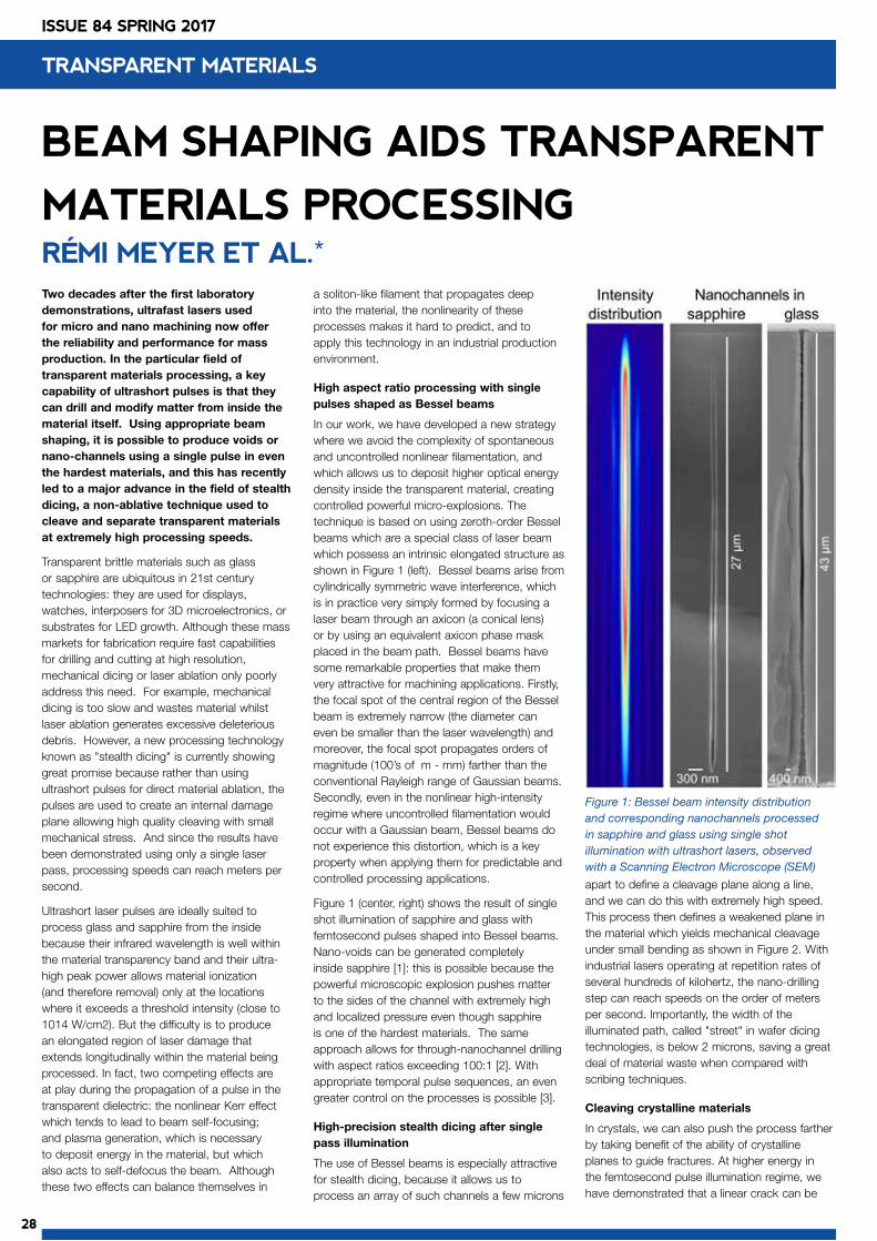
28
ISSUE 84 SPRING 2017
TRANSPARENT MATERIALS
BEAM SHAPING AIDS TRANSPARENT
MATERIALS PROCESSING RÉMI MEYER ET AL.* Two decades after the first laboratory demonstrations, ultrafast lasers used for micro and nano machining now offer the reliability and performance for mass production. In the particular field of transparent materials processing, a key capability of ultrashort pulses is that they can drill and modify matter from inside the material itself. Using appropriate beam shaping, it is possible to produce voids or nano-channels using a single pulse in even the hardest materials, and this has recently led to a major advance in the field of stealth dicing, a non-ablative technique used to cleave and separate transparent materials at extremely high processing speeds.
Transparent brittle materials such as glass or sapphire are ubiquitous in 21st century technologies: they are used for displays, watches, interposers for 3D microelectronics, or substrates for LED growth. Although these mass markets for fabrication require fast capabilities for drilling and cutting at high resolution, mechanical dicing or laser ablation only poorly address this need. For example, mechanical dicing is too slow and wastes material whilst laser ablation generates excessive deleterious debris. However, a new processing technology known as "stealth dicing" is currently showing great promise because rather than using ultrashort pulses for direct material ablation, the pulses are used to create an internal damage plane allowing high quality cleaving with small mechanical stress. And since the results have been demonstrated using only a single laser pass, processing speeds can reach meters per second.
Ultrashort laser pulses are ideally suited to process glass and sapphire from the inside because their infrared wavelength is well within the material transparency band and their ultra-high peak power allows material ionization (and therefore removal) only at the locations where it exceeds a threshold intensity (close to 1014 W/cm2). But the difficulty is to produce an elongated region of laser damage that extends longitudinally within the material being processed. In fact, two competing effects are at play during the propagation of a pulse in the transparent dielectric: the nonlinear Kerr effect which tends to lead to beam self-focusing; and plasma generation, which is necessary to deposit energy in the material, but which also acts to self-defocus the beam. Although these two effects can balance themselves in
a soliton-like filament that propagates deep into the material, the nonlinearity of these processes makes it hard to predict, and to apply this technology in an industrial production environment.
High aspect ratio processing with single pulses shaped as Bessel beams
In our work, we have developed a new strategy where we avoid the complexity of spontaneous and uncontrolled nonlinear filamentation, and which allows us to deposit higher optical energy density inside the transparent material, creating controlled powerful micro-explosions. The technique is based on using zeroth-order Bessel beams which are a special class of laser beam which possess an intrinsic elongated structure as shown in Figure 1 (left). Bessel beams arise from cylindrically symmetric wave interference, which is in practice very simply formed by focusing a laser beam through an axicon (a conical lens) or by using an equivalent axicon phase mask placed in the beam path. Bessel beams have some remarkable properties that make them very attractive for machining applications. Firstly, the focal spot of the central region of the Bessel beam is extremely narrow (the diameter can even be smaller than the laser wavelength) and moreover, the focal spot propagates orders of magnitude (100’s of m - mm) farther than the conventional Rayleigh range of Gaussian beams. Secondly, even in the nonlinear high-intensity regime where uncontrolled filamentation would occur with a Gaussian beam, Bessel beams do not experience this distortion, which is a key property when applying them for predictable and controlled processing applications.
Figure 1 (center, right) shows the result of single shot illumination of sapphire and glass with femtosecond pulses shaped into Bessel beams. Nano-voids can be generated completely inside sapphire [1]: this is possible because the powerful microscopic explosion pushes matter to the sides of the channel with extremely high and localized pressure even though sapphire is one of the hardest materials. The same approach allows for through-nanochannel drilling with aspect ratios exceeding 100:1 [2]. With appropriate temporal pulse sequences, an even greater control on the processes is possible [3].
High-precision stealth dicing after single pass illumination
The use of Bessel beams is especially attractive for stealth dicing, because it allows us to process an array of such channels a few microns
apart to define a cleavage plane along a line, and we can do this with extremely high speed. This process then defines a weakened plane in the material which yields mechanical cleavage under small bending as shown in Figure 2. With industrial lasers operating at repetition rates of several hundreds of kilohertz, the nano-drilling step can reach speeds on the order of meters per second. Importantly, the width of the illuminated path, called "street" in wafer dicing technologies, is below 2 microns, saving a great deal of material waste when compared with scribing techniques.
Cleaving crystalline materials
In crystals, we can also push the process farther by taking benefit of the ability of crystalline planes to guide fractures. At higher energy in the femtosecond pulse illumination regime, we have demonstrated that a linear crack can be
Figure 1: Bessel beam intensity distribution and corresponding nanochannels processed in sapphire and glass using single shot illumination with ultrashort lasers, observed with a Scanning Electron Microscope (SEM)

29
ISSUE 84 SPRING 2017
generated which follows one of the crystalline axes of the material [4]. Moreover, we were able to arbitrarily choose the direction of the cleavage plane among the crystalline axes by varying the polarization of the input laser beam. The important result is that the distance between laser impacts can be increased to several tens of micrometers, thus increasing by a factor 10 the potential writing speed. Figure 3 shows a triangular cut out of sapphire produced with this technique.
What about the future?
It is known that brittle materials need edge polishing to avoid chipping when they are packaged or handled. However, such polishing is energetically costly and delicate. But this is where novel beam shaping techniques suggest a further novel application of ultrafast lasers using “accelerating beams” that curve while they propagate. Although individual rays of light always propagate in a straight line, we can shape a laser beam so that a narrow high intensity region (above the threshold for ablation) can follow an arbitrary curved path known as an optical caustic as shown in Figure 4 [5]. The novel capability of this approach has been shown in demonstrations where we have used accelerating beams to polish the edges of silicon and diamond wafers, as shown in Figure 5 [6].
Conclusion
The application of ultrashort pulsed lasers is undergoing rapid expansion in the field of transparent laser materials processing because of the novel capabilities offered by beam shaping to precisely control how energy is deposited within the material's bulk. State of the art technologies allow us to mark, generate open voids, create high aspect ratio nanochannels, cleave, and create self-cleavage planes all along material depth. This opens a wealth of novel
opportunities to process materials, reduce costly material waste during separation, minimize debris, and to develop processes that are more efficient. This is probably not the end of the story. Our group and others are currently working on improving beam shapes to increase the ability of materials to cleave while reducing the amount of micro-cracks left behind after cleaving. While the beams that are used in these processes are very small, the opportunities of these new technologies appear to be as large as we can imagine.
Acknowledgement
The research leading to these results has received funding from the European Union Seventh Framework Programme [ICT 2013.3.2 Photonics] under grant agreement n°619177 and European Research Council (ERC) under the European Union's Horizon 2020 research and innovation programme (grant agreement No 682032-PULSAR). This work has been performed in cooperation with the Labex ACTION program, contract ANR-11-LABX-0001-01 and partly supported by the French RENATECH network.
References
[1] L. Rapp et al., Scientific Reports, 6, 34286, 2016[2] M. K. Bhuyan et al., Applied Physics Letters, 97, 081102, 2010[3] F. Courvoisier et al, patent WO 2013/153195, EP 2 836 332 B1[4] L. Rapp et al., Optics Express, 25 (8) 9312-9317, 2017[5] A. Mathis et al., Optics Express, 38 (13) 2218-2220, 2013[6] A. Mathis et al., Applied Physics Letters, 101, 071110, 2012
* Rémi Meyer, John Dudley & François Courvoisier, Institut FEMTO-ST, France
Contact: François [email protected]
TRANSPARENT MATERIALS
Rémi Meyer is a PhD student at University of Franche-Comté, France. His main research interest is ultrafast laser-matter interaction with shaped beams
SEE OBSERVATIONS P33
Figure 2: Concept of stealth dicing with non-diffractive beams. Transparent material is processed using Bessel beams to weaken the targeted fracture plane and in a second step cleaving occurs under a small bending
Figure 3: Sapphire sample cleaved in a triangle shape after ultrashort Bessel beam processing. Right SEM pictures show the cleaved edges aspect respectively from top and side views
Figure 4: Concept of material processing using accelerating beams. Multiple passes are required for curved edge polishing.
Figure 5: Examples of brittle materials curved polishing: SEM pictures of diamond and silicon processed with accelerating beams.
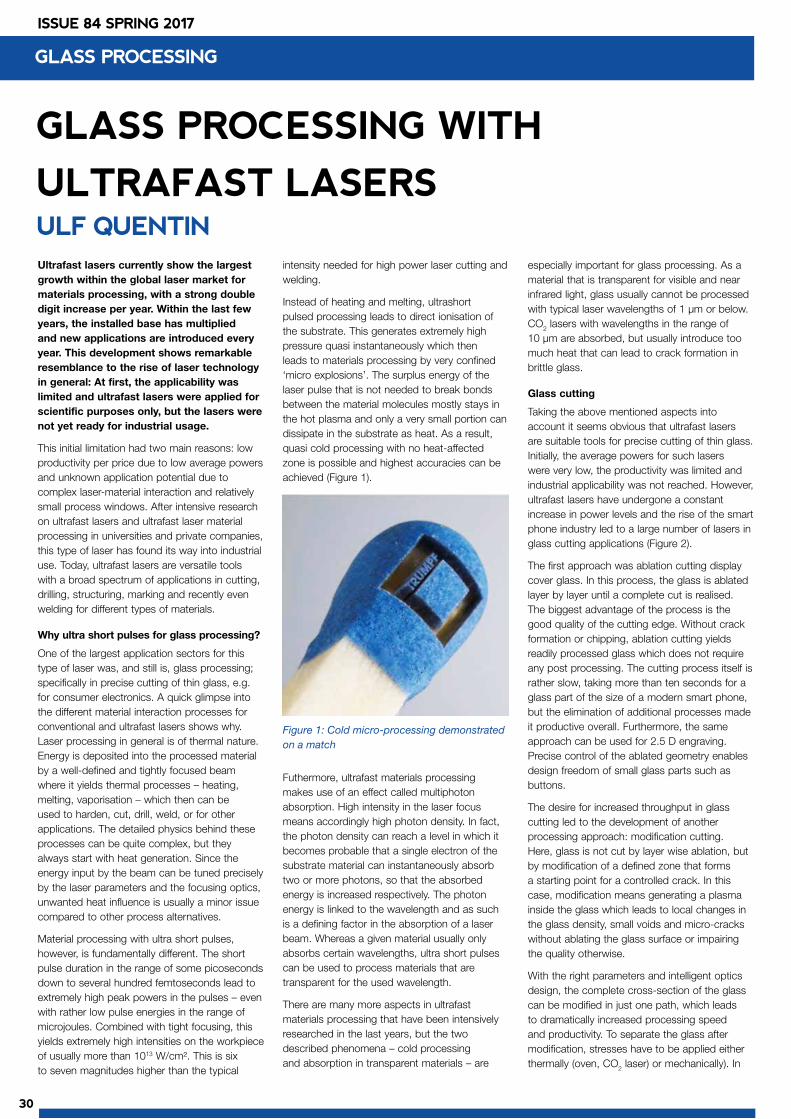
30
ISSUE 84 SPRING 2017
GLASS PROCESSING WITH
ULTRAFAST LASERS ULF QUENTIN
GLASS PROCESSING
Ultrafast lasers currently show the largest growth within the global laser market for materials processing, with a strong double digit increase per year. Within the last few years, the installed base has multiplied and new applications are introduced every year. This development shows remarkable resemblance to the rise of laser technology in general: At first, the applicability was limited and ultrafast lasers were applied for scientific purposes only, but the lasers were not yet ready for industrial usage.
This initial limitation had two main reasons: low productivity per price due to low average powers and unknown application potential due to complex laser-material interaction and relatively small process windows. After intensive research on ultrafast lasers and ultrafast laser material processing in universities and private companies, this type of laser has found its way into industrial use. Today, ultrafast lasers are versatile tools with a broad spectrum of applications in cutting, drilling, structuring, marking and recently even welding for different types of materials.
Why ultra short pulses for glass processing?
One of the largest application sectors for this type of laser was, and still is, glass processing; specifically in precise cutting of thin glass, e.g. for consumer electronics. A quick glimpse into the different material interaction processes for conventional and ultrafast lasers shows why. Laser processing in general is of thermal nature. Energy is deposited into the processed material by a well-defined and tightly focused beam where it yields thermal processes – heating, melting, vaporisation – which then can be used to harden, cut, drill, weld, or for other applications. The detailed physics behind these processes can be quite complex, but they always start with heat generation. Since the energy input by the beam can be tuned precisely by the laser parameters and the focusing optics, unwanted heat influence is usually a minor issue compared to other process alternatives.
Material processing with ultra short pulses, however, is fundamentally different. The short pulse duration in the range of some picoseconds down to several hundred femtoseconds lead to extremely high peak powers in the pulses – even with rather low pulse energies in the range of microjoules. Combined with tight focusing, this yields extremely high intensities on the workpiece of usually more than 1013 W/cm². This is six to seven magnitudes higher than the typical
intensity needed for high power laser cutting and welding.
Instead of heating and melting, ultrashort pulsed processing leads to direct ionisation of the substrate. This generates extremely high pressure quasi instantaneously which then leads to materials processing by very confined ‘micro explosions’. The surplus energy of the laser pulse that is not needed to break bonds between the material molecules mostly stays in the hot plasma and only a very small portion can dissipate in the substrate as heat. As a result, quasi cold processing with no heat-affected zone is possible and highest accuracies can be achieved (Figure 1).
Futhermore, ultrafast materials processing makes use of an effect called multiphoton absorption. High intensity in the laser focus means accordingly high photon density. In fact, the photon density can reach a level in which it becomes probable that a single electron of the substrate material can instantaneously absorb two or more photons, so that the absorbed energy is increased respectively. The photon energy is linked to the wavelength and as such is a defining factor in the absorption of a laser beam. Whereas a given material usually only absorbs certain wavelengths, ultra short pulses can be used to process materials that are transparent for the used wavelength.
There are many more aspects in ultrafast materials processing that have been intensively researched in the last years, but the two described phenomena – cold processing and absorption in transparent materials – are
especially important for glass processing. As a material that is transparent for visible and near infrared light, glass usually cannot be processed with typical laser wavelengths of 1 µm or below. CO2 lasers with wavelengths in the range of 10 µm are absorbed, but usually introduce too much heat that can lead to crack formation in brittle glass.
Glass cutting
Taking the above mentioned aspects into account it seems obvious that ultrafast lasers are suitable tools for precise cutting of thin glass. Initially, the average powers for such lasers were very low, the productivity was limited and industrial applicability was not reached. However, ultrafast lasers have undergone a constant increase in power levels and the rise of the smart phone industry led to a large number of lasers in glass cutting applications (Figure 2).
The first approach was ablation cutting display cover glass. In this process, the glass is ablated layer by layer until a complete cut is realised. The biggest advantage of the process is the good quality of the cutting edge. Without crack formation or chipping, ablation cutting yields readily processed glass which does not require any post processing. The cutting process itself is rather slow, taking more than ten seconds for a glass part of the size of a modern smart phone, but the elimination of additional processes made it productive overall. Furthermore, the same approach can be used for 2.5 D engraving. Precise control of the ablated geometry enables design freedom of small glass parts such as buttons.
The desire for increased throughput in glass cutting led to the development of another processing approach: modification cutting. Here, glass is not cut by layer wise ablation, but by modification of a defined zone that forms a starting point for a controlled crack. In this case, modification means generating a plasma inside the glass which leads to local changes in the glass density, small voids and micro-cracks without ablating the glass surface or impairing the quality otherwise.
With the right parameters and intelligent optics design, the complete cross-section of the glass can be modified in just one path, which leads to dramatically increased processing speed and productivity. To separate the glass after modification, stresses have to be applied either thermally (oven, CO2 laser) or mechanically). In
Figure 1: Cold micro-processing demonstrated on a match
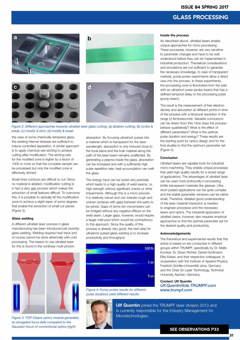
31
ISSUE 84 SPRING 2017
the case of some chemically tempered glass, the existing internal stresses are sufficient to induce controlled separation. A similar approach is to apply chemical wet etching to achieve cutting after modification. The etching rate for the modified zone is higher by a factor of 1000 or more so that the complete sample can be processed but only the modified zone is effectively etched.
Small inner contours are difficult to cut: Since no material is ablated, modification cutting is in fact a zero gap process which makes the extraction of small features difficult. To overcome this, it is possible to optically tilt the modification zone to achieve a slight taper of some degrees that enable the extraction of small cut pieces (Figure 3).
Glass welding
A different ultrafast laser process in glass manufacturing has been introduced just recently: glass welding. Welding requires heat input and of course cannot be done athermally with cold processing. The reason to use ultrafast laser for this is found in the nonlinear multi-photon
absorption. By focusing ultrashort pulses into a material which is transparent for the laser wavelength, absorption is only induced close to the focal plane and the bulk material along the path of the laser beam remains unaffected. By generating a plasma inside the glass, absorption can be increased and with a sufficiently high pulse repetition rate, heat accumulation can melt the glass.
The energy input can be tuned very precisely which leads to a high quality of weld seams, i.e. high strength without significant cracks or other impairments. Although this is a micro process it is relatively robust and can tolerate rough and uneven surfaces with gaps between the parts to be joined. Gaps of some ten micrometers can be bridged without any negative effects on the weld seam. Larger gaps, however, would require a larger melt pool which would be contradictory to this approach. Since the quality of this process is already very good, the next step for ultrashort pulsed glass welding is to increase productivity and throughput.
Inside the process
As described above, ultrafast lasers enable unique approaches for micro processing. These processes, however, are very sensitive to parameter changes and have to be well understood before they can be implemented in industrial production. Theoretical considerations and simulations are not sufficient to generate the necessary knowledge. In case of transparent material, pump-probe experiments allow a direct view into the process. In these experiments, the processing zone is illuminated from the side with an ultrashort pulse (probe beam) that has a defined temporal delay to the processing pulse (pump beam).
The result is the measurement of free electron density and absorption at different points in time of the process with a temporal resolution in the range of femtoseconds. Valuable conclusions can be drawn from this: How does the process behave qualitatively? What is the effect of different parameters? What is the optimal pulse duration and energy? These results are the starting point for optics design and for the final studies to find the optimum parameter set (Figure 4).
Conclusion
Ultrafast lasers are capable tools for industrial micro-machining. They enable unique processes that yield high quality results for a broad range of applications. The advantages of ultrafast laser can be used most profoundly in processing brittle transparent materials like glasses. Ultra short pulsed applications can be quite complex and the stable parameter windows can be rather small. Therefore, detailed good understanding of the laser material interaction is needed to engineer processes and the necessary lasers and optics. The industrial application of ultrafast lasers, however, also requires empirical approaches to find the optimal parameter set for the desired quality and productivity.
Acknowledgements
The theoretical and experimental results that this article is based on are conducted in different groups within TRUMPF, specifically by Dr. Malte Kumkar, Dr. Sören Richter, Daniel Großmann, Elke Kaiser, and their respective colleagues, in cooperation with the Institute of Applied Physics, Friedrich-Schiller-Universität Jena, Germany and the Chair for Laser Technology, Technical University Aachen, Germany.
Contact: Ulf [email protected]
GLASS PROCESSING
Ulf Quentin joined the TRUMPF laser division 2013 and is currently responsible for the Industry Management for Microtechnologies.
SEE OBSERVATIONS P33
Figure 2: Different approaches towards ultrafast laser glass cutting: (a) ablation cutting; (b) scribe & break; (c) modify & etch; (d) modify & break
Figure 3: TOP Cleave optics module generates an elongated focus (left) compared to the Gaussian focus of conventional optics (right)
Figure 4: Pump-probe results for different pulse durations yield different results
a b
dc

32
ISSUE 84 SPRING 2017
OBSERVATIONS
NUCLEAR WELDING: POTENTIAL AND CHALLENGES FOR LASERSNeil Irvine & John Francis
Narrow-gap laser welding (NGLW) is not a particularly new approach – NGLW research dates back to the mid-1980s – and is already used in at least two industrial applications (both of these are stainless steel). However, advances in fibre-delivered laser sources and industry demand has driven several researcher institutes to revisit this approach, mainly focusing on nuclear applications.
The results presented in this work are part of a much larger body of excellent work undertaken in the NNUMAN project, and are encouraging for the application of this technology to primary nuclear components. Particularly as they have been achieved on industry-relevant materials and with industry-relevant PWHTs. The anticipated productivity benefit c.f. traditional arc-welding techniques was not realised, but it would be interesting to know if inter-pass cleaning and inspection activities were included in this calculation; since the fewer passes in a NGLW may provide significant benefit once these are taken into account.
A multi-head NGLW approach would also provide productivity benefit, particularly as I doubt the full capability of the 16kW laser source was used to produce these welds. Furthermore, on-going developments in narrow-groove sensing equipment for adaptive control of arc-welding, combined with appropriate oscillation of the laser beam, could be applied to NGLW to address some of the challenges associated with scaling this technology up to component level.
Qualification of this technology for the nuclear industry may be a step too far, given the relatively low volumes of structures required. A more achievable application may be wind-turbine towers (jackets and/or monopoles), since the projected market demand over the next twenty years is considerable, the thicknesses of interest are more readily achievable with NGLW, and the manufacturing volumes would allow tighter control of fit-up and orality tolerances.
Jon Blackburn, TWI
It’s very easy to write a paper that promotes solutions whilst glossing over real challenges – it’s much harder to talk about those challenges, especially when it’s your research team that is pouring heart and soul into developing the solutions. Here however, Neil and John have presented a thorough, and very honest, overview of the work of the NNUMAN team to date. It is apparent that the potential gains that may have been purported for NGLW may be slimmer than many would have wanted, but it doesn’t mean
that the technique should be book-shelved just yet. For good reason, this research is ongoing (it may not be to the original plan but this is cutting-edge applications research and to paraphrase Moltke the Elder, ‘no battle plan survives contact with the enemy’) and whilst Neil and John have shown that the NNUMAN team are going to have to be very clever to develop those solutions, this paper shows that the development of NGLW is in very good hands.
Nicholas Blundell, MTC
LASER POLISHING: A FLEXIBLE APPROACH FOR SMOOTHING SURFACESWojciech Gora
Laser polishing is an attractive post-processing technique for AM parts due to its spatial selectivity and effectiveness in reducing the high initial surface roughness. The article highlights very well these advantages in post-processing CoCr and Ti6Al4V AM parts that are widely used as medical implants. However, while macro laser polishing is very effective in improving the surface roughness it creates a re-cast layer with high residual stresses and also it has different material microstructure/properties than the balk. At the same time micro laser polishing is much more “gentle” to the surface and allow the geometrical accuracy achieved with proceeding processes to be retained. Thus, as it is stated in the article the two laser polishing processes are complementary and can be used in sequence to achieve the best final result.
Stefan Dimov, University of Birmingham
IMPROVED SURFACE TEXTURING FOR INDUSTRIAL APPLICATIONS Olivier Allegre et al.
Generating laser-induced periodic surface structures (LIPSS) is an extremely important surface engineering technique. It offers flexibility in terms of feature geometry and performance characteristics, whilst being easily produced with a wide range of potential applications. This means that LIPSS offer a more effective approach to texturing than lithography and should, therefore, could be key process in industry.
This team from the UK and Germany have shown polarisation and intensity profile to be a viable means for process control. This
is particularly pertinent at this time to LIPSS because for wider industrial take up the process needs to be scalable, which is largely achieved through stable, accurate and repeatable process control. The work and findings described in this article bring us closer to realizing fully industrial scale LIPSS processing and applications.
Jonathan Lawrence, Coventry University
The article presents recent developments from the authors in the generation of LIPSS textures on the surface of a laser irradiated substrate. LIPSS, which stands for Laser Induced Periodic Surface Structures, are essentially organised ripples with sub-micrometre period. These can be obtained from laser irradiation with short and ultra-short pulses under certain conditions. While the formation of such periodic features is well reported in the laser literature, the reader will take interest in the authors’ work as it focuses on the implementation of polarisation and beam profile intensity shaping techniques. In particular, these are applied to optimise the throughput and the large area patterning of LIPSS processing. Within the MEMS and semi-conductor fabrication sectors, a number of lithography techniques for the production of such periodic features have already been proposed.
In contrast, the potential for lasers to provide an alternative manufacturing route is perhaps well less-known outside the laser community. However, a key intrinsic advantage of lasers for this purpose is the wide range of materials that can be processed to enable not only optical but also mechanical or chemical applications of such surface textures. This potential is demonstrated by the authors in this article. Indeed, based on the developed polarisation and wavefront shaping techniques, the authors reports the formation of LIPSS textures on various materials including stainless steel and indium tin oxide coating.
Emmanuel Brousseau, Cardiff University
PRECISION MICROPROCESSING WITH HIGH POWER, ULTRAFAST LASERSDimitris Karnakis
It is very interesting to learn how new laser architectures might take Ti:Sapphire lasers beyond the traditional spectroscopy and imaging markets, entering into the laser materials processing space. The combination of femtosecond pulses and megahertz pulse rates will be attractive to those processing transparent materials, by providing increased quality along

33
ISSUE 84 SPRING 2017
with process rates and without the need to resort to UV. One would expect the commercial success to be linked to availability of suitable high power green pump lasers operating at 300W and above.
Mark Thompson, IPG Photonics
Short pulse lasers have a great value in material processing and this article explains why this is the case. More importantly, it shows the value of a good consortium and the type of development that can come from them.
As machine users, builders and process developers, we all want low cost, high power, reliable, flexible frequency, short pulse lasers and this sounds like another step towards this goal.
It is always important to remember that many processes can work very well using a trusty low cost nano-second laser but short pulse lasers open the possibility for many new applications, and a success of some that have previously failed because this technology was not available at a reasonable price.
Neil Sykes, Micronanics
BEAM SHAPING AIDS TRANSPARENT MATERIALS PROCESSING Rémi Meyer et al.
I was very interested to read Remi Meyer’s article, and the theme of laser processing of transparent materials was a very well-represented one at ILAS. The application of tough, transparent materials in industry, particularly in the consumer electronics sector, is showing growth potential higher than might be expected and whilst many markets have sought to replace glass (in bottles and drinking vessels for example), the toughness and scratch resistance that they offer is something we have come to rely on in our smartphones, tablets and watches.
The ability to cut transparent and brittle materials with crack-free edges and all required geometries is a challenge that Nadeem Rizvi explores in his observation on the article by Ulf Quentin – cost versus speed is of greatest interest to the markets where volumes and values are high enough to justify the capital spend. Potential to cut with speeds of several (or perhaps 10’s) of metres/second is necessary for those markets where there are millions of identical components per year, but I don’t see job shops buying glass cutting systems of this type in the near future.Polishing by “accelerating beams” is also a new concept to me, and I look forward to reading about some real-world applications for this too.
It would be good to learn where the market potential is for this, or whether it is a solution looking for a problem (still worthy of research!).
Most interesting to me was that Meyer and several other ILAS presenters (Sugioka, Geremia, Allegre and Quentin to name a few) mentioned Bessel beams in their talks. Although I have been exposed to a fair amount of technical material about processing of glass and sapphire with filamentation and stealth dicing, I hadn’t heard of the Bessel beam until ILAS. As often happens, when you discover a new word or topic, it appears to crop up several times in quick succession afterwards. I was intrigued at the brief insight Meyer brings to this topic and feel certain that I shall hear a lot more about this process in the months and years to come. Especially intriguing to engineers like myself is the ability to create a non-diffracting beam capable of attaining a focal diameter less than the wavelength (what kind of magic is this?!). This concept seems very useful for the applications outlined, cutting and drilling in the sub-micron scale. Tell me more!
Dave MacLellan, AILU
GLASS PROCESSING WITH ULTRAFAST LASERS Ulf Quentin
Processing of glass and the use of ultrafast lasers have both grown enormously in the past three years so this is a timely update on Trumpf’s technologies and is very useful in presenting a broad picture of current approaches.
Of the four glass cutting processes which are discussed, the ablative cutting is the most straightforward and easiest to implement with ‘standard’ optics, i.e. it does not require special expensive optics and ablative cutting can be done in a single step in air with little or no post-processing. The latest ‘modify and break’ techniques are obviously attractive from the viewpoint of producing zero kerf and no cracking but do require a very large capital outlay for the whole system.
The ‘modify and self-break’ techniques have obviously found a good fit within the mobile/display devices sector where there is a requirement for massive volumes of glass cutting. I suspect, however, that they will not be accessible to most ‘ordinary’ (lower-volume) users, those who do not have really deep pockets and large production facilities in which the high-power ultrafast lasers and the ultra-special filamentation modules reside. Nonetheless, the results from the ‘modify and self-break’ systems are highly impressive, both from a pure physics and an engineering viewpoint.
A few additional points are worth noting: (a) glass can be processed reasonably well with nanosecond visible and nanosecond DUV lasers so ultrafast lasers are not the only option out there. The issue becomes one of the quality that one can withstand in an application – if crack-free edge quality is needed then ultrafast lasers will be the way to go but many applications would not require this, hence nanosecond processing of glass remains a valid, and much cheaper, option; (b) it is interesting that one of the consequences of zero kerf cutting is that it is difficult to extract an internally-cut shape. The solution – making a slope or taper to the sidewalls – mimics nicely what usually occurs in most laser standard cutting systems (i.e. a sloping sidewall is produced in standard laser ablation processes); (c) glass welding is introduced but not detailed and it will be very interesting to hear more about this, possibly in a follow-on article.
Nadeem Rizvi, Laser Micromachining Ltd.
WOULD YOU LIKE TO WRITE FOR ‘THE LASER USER’?We are looking for new content to make The Laser User more interesting, relevant and entertaining to read.
If you would be interested in contributing to the magazine, we would love to have your input and we will do our best to use your words and high resolution images.
We need:
• Press releases
• Personnel & business news
• Technical articles
• Observations
• Anecdotes
• Case studies
• Interviews
• Application guides
• Tips and tricks
To submit content contact [email protected]
OBSERVATIONS

34
ISSUE 84 SPRING 2017
Confirmed exhibitors in the AILU-hosted Laser Manufacturing Hub at Advanced Engineering 2017 (layout shown left) are:
• Cyan Tec Systems
• ACSYS Lasertechnik UK
• Laser SOS
• Carrs Welding & Micrometric
• Laser Lines
• IPG Photonics
• Fimark
• Croft Flters & Croft AM
• TLM Laser
• Bystronic
This will be the first year we will have a dedicated zone for our sector, right in the middle of the exhibition and within the Performance Metals Engineering Zone – as you can see it is already almost sold out – act fast if you want to exhibit, and contact the AILU office if you are interested in joining the Hub in 2018 where it will be a larger area.
Alongside the exhibition is the Open Conference – talk to me if you would like to offer a talk in the Performance Metals Session, it would be great to have more laser case studies and applications presented. As in the past 2 years I will be giving an overview of what lasers can do.
Dave [email protected]
A FUNNY THING...
One of the most iconic James Bond images featuring a laser is the one with the villainous Goldfinger standing over James Bond (Sean Connery) and watching as a laser beam inches closer to Bond who is strapped down on a slab of “pure gold”. Throughout my career I have used this image to illustrate many talks (especially to those less familiar with lasers rather than to the laser community) to highlight how wrong the movie makers were about lasers and how the reality is quite different.
During the opening Plenary Session at ILAS 2017, Paul Hilton also included a brief mention of the James Bond movie and an episode of Tomorrow’s World from the year 1967 where the first industrial laser cut was reprised and the Bond film referenced – referring to the first laser cut with assist gas by Peter Houldcroft of TWI in that year, 50 years ago.
Returning to Goldfinger, one vital fact that I didn’t appreciate or consider until now, is that the movie Goldfinger came out in 1964 and the book was written by Ian Fleming in 1959 – the year before the invention of the laser. Obviously (with hindsight) the laser wasn’t featured in the book, instead Bond was due to be cut in two by a circular saw. When transferring the novel to the screen, the screenwriters decided to substitute a futuristic cutting tool and chose the newly introduced “laser” for the task. The screenwriters clearly found out a bit about lasers, and allegedly they purchased a visible laser – but found it wasn’t bright enough with all the studio lights so they had to colour it in brighter in post-production. The actual cutting in the film was produced with an oxyacetylene torch lying hidden underneath, apparently coming close to actually burning Connery in the process when
he didn’t hear the word “Cut” (or perhaps he misconstrued the meaning?)
In many ways, finding out more about the history of technology imagined in film forces me to revise my view of the innovation in cinema versus science. The first video conversation “Metropolis” (1927), the first mobile “flip-phone” from Star Trek (1967), the first tablet computer in 2001: A Space Odyssey (1968) and the driverless car KITT from the TV series “Knight Rider” (1982) all appeared decades before the real-world technology caught up (and often surpassed) the imagined experience.
When I review the progress of the laser in the first 57 years, as well as the integrated circuit, developed around the same time, it is impressive to think about the pace of progress.
Smaller, cheaper, more efficient, more reliable – in many cases a “fit and forget” black box (other colours are available).
I recall wondering whether automation and robotics would lead to mass unemployment, as long ago as when I was leaving school – a concept that has been in the news again this year. Will the robots replace all of our jobs? Who can say – except that when we consider that the number of jobs created by 5 of today’s leading tech companies: Google, Amazon, Apple, Microsoft and Foxconn is close to 2 million – not counting the suppliers that depend on them - and none of these companies existed 50 years ago. Maybe the moral of the tale is – predicting the future is difficult!
Dave [email protected]
I EXPECT YOU TO DIE MR BOND
AILU LASER MANUFACTURING HUB AT ADVANCED ENGINEERING 2017

35
ISSUE 84 SPRING 2017
FORTHCOMING EVENTS
AILU WORKSHOPPresentations, Exhibition, Networking
LASERS IN BIOTECHNOLOGY (LiB '17)
15 JUNE 2017 Bibliotheque Marie-Curie, INSA, Lyon , FranceAILU is running a 1-day workshop in Lyon, France to reach out to organisations in Europe with an interest in laser applications in Biotechnology. Lasers are used in surgical applications (eyesight correction, tattoo removal, cosmetic surgery etc.) as well as the more traditional manufacturing of medical devices or surgical tools. This is the first of a series of non-UK workshops.
Confirmed speakers
Lin Li University of Manchester, UK Laser manufacturing of stents Robert Thomson Heriot Watt University UK Ultrafast laser inscription of photonic microoptic components for endoscopic applications Romain Royon Irisiome Solutions, France New laser technology for tattoo removal and laser in dermatologyLuca Romali University of Parma, Italy Towards high throughput laser texturing of antibacterial surfaces on stainless steelChris Randon OpTek Systems, UK Laser micromachining for next-generation diagnostics and therapeuticsDavid Waugh Coventry University, UK To be confirmedJassem Safioui FEMTO Engineering, France To be confirmed
For more information go to www.ailu.org.uk/events
To register contact the AILU office: [email protected]
Book now m m www.advancedengineeringuk.comAEROENGINEERING2017
ADVANCED ENGINEERING2017
COMPOSITESENGINEERING2017
AUTOMOTIVEENGINEERING2017
PERFORMANCE METALSENGINEERING2017
1 & 2 November 2017, NEC, Birmingham
1 & 2 November 2017, NEC, Birmingham
ADVANCED ENGINEERING20171 & 2 November 2017, NEC, Birmingham
1 & 2 November 2017, NEC, Birmingham
1 & 2 November 2017, NEC, Birmingham
1 & 2 November 2017, NEC, Birmingham
The UK’s largest annual gathering of advanced engineering professionals
AEROENGINEERING
ADVANCED ENGINEERING
COMPOSITESENGINEERING
AUTOMOTIVEENGINEERING
PERFORMANCE METALSENGINEERING
ADVANCED ENGINEERING1 & 2 November 2017, NEC, Birmingham
Advanced Engineering is the industry event where high-technology manufacturing sectors converge under one roof to meet and do business. Join us where the familiar and the unfamiliar collide to provide new opportunities across the engineering supply chain.
AEROENGINEERING
ADVANCED ENGINEERING
COMPOSITESENGINEERING
AUTOMOTIVEENGINEERING
PERFORMANCE METALSENGINEERING
ADVANCED ENGINEERING1 & 2 November 2017, NEC, Birmingham
AEROENGINEERING
ADVANCED ENGINEERING
COMPOSITESENGINEERING
AUTOMOTIVEENGINEERING
PERFORMANCE METALSENGINEERING
ADVANCED ENGINEERING1 & 2 November 2017, NEC, Birmingham AERO
ENGINEERING
ADVANCED ENGINEERING
COMPOSITESENGINEERING
AUTOMOTIVEENGINEERING
PERFORMANCE METALSENGINEERING
ADVANCED ENGINEERING1 & 2 November 2017, NEC, Birmingham
AE2017_Advert190x125NEW.indd 1 20/04/2017 15:17:49

36
ISSUE 84 SPRING 2017
March 2017 April 2017 May 2017 June 2017
22-23ILAS 20175TH INDUSTRIAL LASER APPLICATIONS SYMPOSIUMBelton Woods Hotel, Grantham
24-27 SPIE OPTICS + OPTOELECTRONICS 2017Prague, Czech Republic
18AILU AGM & NATIONAL STRATEGY WORKSHOPInstitute for Advanced Manufacturing and Engineering, Coventry
5-8LASER PRECISION MICROFABRICATION (LPM2017)Toyama, Japan
15AILU WORKSHOPLASERS IN BIOTECHNOLOGY INSA, Lyon, France
20-23 EPHJ - EMPT - SMT High Precision Fair
26-29 LASERS IN MANUFACTURING (LiM)Munich, Germany
July/August 2017 September 2017 October 2017 November 2017
17-22EUROMAT 2017Thessaloniki, Greece
13AILU WORKSHOPLASER CLEANING
18ANNUAL JOB SHOP MEETING
22-26ICALEOAtlanta, USA
1-2ADVANCED ENGINEERING 2017with AILU Laser Manufacturing HubNEC, Birmingham
23AILU WORKSHOPLASER APPLICATIONS IN LIGHTWEIGHT STRUCTURES
EVENTS: RECENT AND FUTURE
Image courtesy CleanLASER
Image courtesy TRUMPF
Image courtesy Coherent ROFIN
AGM
More images available on the AILU Facebook page