5 - 18 GHz Low-Noise MMIC Amplifier Data Sheet ... gain of 19 dB and Noise Figure of 3 dB @ 12 GHz....
6
• Wide Band: 5 to 18 GHz • NF (ext match): 3.4 dB @ 6 GHz 3.0 dB @ 12 GHz 3.7 dB @ 18 GHz • P-1dB: 21 dBm • OIP3: 29 dBm • Gain: 19 db • Bias Condition: VDD = 4.5V IDD = 135 mA • 50-Ohm On-chip Matching • Unconditionally Stable from 50 MHz to 20 GHz FEATURES APPLICATIONS MLA-06183A-M4 5 - 18 GHz Low-Noise MMIC Amplifier Data Sheet • Microwave Radios • Satellite Communications • Commercial Wireless Systems ELECTRICAL SPECIFICATIONS: VDD1, VDD2=+4.5V,VG2/VG2=-0.025 (2) , IDD=135mA, Ta=25 C, ZO=50 ohm (1) DESCRIPTION The MLA-06183A-M4 is a fully-matched 2-stage broadband low-noise MMIC amplifier utilizing high-reliability low-noise GaAs PHEMT technology. This MMIC is suited for microwave radios, wideband EW, satellite communications, instrumentation, and commercial communication systems, where low-noise figure and high-gain are desirable. It has excellent gain of 19 dB and Noise Figure of 3 dB @ 12 GHz. Typical P-1dB is 21 dBm and OIP3 is + 29 dBm @ 12 GHz. It has on-chip bias circuit, choke, and DC blocking to provide bias stability and ease of use. PARAMETER TEST CONDITIONS TYPICAL DATA UNITS Frequency Range 5-18 GHz Gain 6 - 8 GHz 8 - 14 GHz 14 - 17.5 GHz 18 GHz 20 19 18 16 dB Gain Flatness 6 - 14 GHz 14 - 18 GHz 0.75 1.25 +/-dB Input Return Loss 6 - 14 GHz 14 - 18 GHz 9 12 dB Output Return Loss 12 dB Output P1dB 6 GHz 12 GHz 18 GHz 17 21 22 dBm Output IP3 @ 0 dBm/tone, 1 MHz separation 6 GHz 12 GHz 18 GHz 29 29 27 dBm Noise Figure 6 GHz 12 GHz 18 GHz 3.4 3.0 3.7 dB Operating Bias Conditions: VDD1, VDD2 IDD VG1,VG2=-0.025V, typical + 4.5 135 V mA Stability Factor K 0.05 to 20 GHz > 1 (1) All data is measured on 50 Ohm carrier, w ith Dual-Bias Supply and stub tuning show n in the datasheet assembly diagram. (2) Since the VG bias setting has typical range of -0.1 to +0.1V, VG1, VG2 bias inputs may be directly grounded/bonded to DC ground to convert to single +ve supply operation such that VG = 0V. The bias current w ill then be fixed and cannot be controlled or shut dow n by VG input. • Surface Mount, RoHs Compliant QFN 4x4mm package MicroWave Technology, Inc. an IXYS Company, 4268 Solar Way, Fremont, CA 94538 510-651-6700 FAX 510-952-4000 WEB www.mwtinc.com Data contained herein is subject to change without notice. All rights reserved © Please visit MwT website www.mwtinc.com for information on other MwT MMIC products. Page 1 of 6, Updated July 2017
Transcript of 5 - 18 GHz Low-Noise MMIC Amplifier Data Sheet ... gain of 19 dB and Noise Figure of 3 dB @ 12 GHz....
• Wide Band: 5 to 18 GHz• NF (ext match): 3.4 dB @ 6 GHz
3.0 dB @ 12 GHz3.7 dB @ 18 GHz
• P-1dB: 21 dBm• OIP3: 29 dBm• Gain: 19 db• Bias Condition: VDD = 4.5V
IDD = 135 mA• 50-Ohm On-chip Matching• Unconditionally Stable from 50 MHz to 20 GHz
FEATURES APPLICATIONS
MLA-06183A-M4 5 - 18 GHz Low-Noise MMIC Amplifier
Data Sheet
• Microwave Radios• Satellite Communications• Commercial Wireless Systems
ELECTRICAL SPECIFICATIONS: VDD1, VDD2=+4.5V,VG2/VG2=-0.025 (2), IDD=135mA, Ta=25 C, ZO=50 ohm (1)
DESCRIPTIONThe MLA-06183A-M4 is a fully-matched 2-stage broadband low-noise MMIC amplifier utilizing high-reliability low-noise GaAs PHEMT technology. This MMIC is suited for microwave radios, wideband EW, satellite communications, instrumentation, and commercial communication systems, where low-noise figure and high-gain are desirable. It has excellent gain of 19 dB and Noise Figure of 3 dB @ 12 GHz. Typical P-1dB is 21 dBm and OIP3 is + 29 dBm @ 12 GHz. It has on-chip bias circuit, choke, and DC blocking to provide bias stability and ease of use.
P ARAM ETER TES T CONDITIONS TYP ICAL DATA UNITSFrequency Range 5-18 GHz
Gain
6 - 8 GHz8 - 14 GHz
14 - 17.5 GHz18 GHz
20191816
dB
Gain F latness 6 - 14 GHz14 - 18 GHz
0.751.25
+ /-dB
Input Return Loss 6 - 14 GHz14 - 18 GHz
912
dB
Output Return Loss 12 dB
Output P 1dB6 GHz
12 GHz18 GHz
172122
dBm
Output IP 3 @ 0 dB m /tone, 1 M Hz separation
6 GHz12 GHz18 GHz
292927
dBm
Noise F igure6 GHz
12 GHz18 GHz
3.43.03.7
dB
Operating B ias Conditions : VDD1, V DD2 IDD
V G1,V G2= -0.025V , typical + 4.5135
Vm A
S tability Fac tor K 0.05 to 20 GHz > 1(1) A ll data is meas ured on 50 Ohm c arr ier, w ith Dual-Bias Supply and s tub tuning s how n in the datas heet as s embly diagram.(2) Sinc e the V G bias s etting has ty pic al range of -0.1 to +0.1V , V G1, V G2 bias inputs may be direc tly grounded/bonded to DC ground to c onv ert to s ingle +v e s upply operation s uc h that V G = 0V . The bias c urrent w ill then be f ix ed and c annot be c ontrolled or s hut dow n by V G input.
• Surface Mount, RoHs Compliant QFN 4x4mm package
MicroWave Technology, Inc. an IXYS Company, 4268 Solar Way, Fremont, CA 94538 510-651-6700 FAX 510-952-4000 WEB www.mwtinc.com
Data contained herein is subject to change without notice. All rights reserved © Please visit MwT website www.mwtinc.com for information on other MwT MMIC products.
Page 1 of 6, Updated July 2017

TYPICAL RF PERFORMANCE: VDD1, VDD2=+4.5V,VG2/VG2=-0.025 (2), IDD=135mA, Ta=25 C, ZO=50 ohm (1)
Ga in ve rsus Fre que ncy & Te m p
10
12
14
16
18
20
22
5 6 7 8 9 10 11 12 13 14 15 16 17 18Fre que ncy (GHz )
Gai
n (d
B)
25 C -40 C 85 C
Input Re turn Loss versus Fre que ncy & Te m p
-30
-25
-20
-15
-10
-5
5 6 7 8 9 10 11 12 13 14 15 16 17 18Fre que ncy (GHz)
Inpu
t Ret
urn
Loss
(dB)
25 C -40 C 85 C
Output Re turn Loss ve rsus Fre que ncy & Te m p
-30
-25
-20
-15
-10
-5
5 6 7 8 9 10 11 12 13 14 15 16 17 18
Fre que ncy (GHz)
Out
put R
etur
n Lo
ss (d
B)
25 C -40 C 85 CIsola tion ve rsus Fre que ncy & Te m p
-60
-50
-40
-30
-20
5 6 7 8 9 10 11 12 13 14 15 16 17 18
Fre que ncy (GHz)
Isol
atio
n (d
B)
25 C -40 C 85 C
C o rre cte d NF ve rsu s F re q u e n cy
2.42.6
2.83
3.23.4
3.63.8
4
5 6 7 8 9 10 11 12 13 14 15 16 17 18F re q u e n cy (G Hz )
Nois
e Fi
gure
(dB)
4 .5V ,134mA 3 .5V ,1 00mAP-1d B & O IP3 v e rsu s F re q u e n cy
161820222426283032
5 6 7 8 9 10 11 12 13 14 15 16 17 18Fre que ncy (GHz )
P-1d
B/O
IP3
(dBm
)
P-1dB, 4.5V ,134mA OIP3, 4.5V ,134mA
MLA-06183A-M4 5 - 18 GHz Low-Noise MMIC Amplifier
Data Sheet
MicroWave Technology, Inc. an IXYS Company, 4268 Solar Way, Fremont, CA 94538 510-651-6700 FAX 510-952-4000 WEB www.mwtinc.com
Data contained herein is subject to change without notice. All rights reserved © Please visit MwT website www.mwtinc.com for information on other MwT MMIC products.
Page 2 of 6, Updated July 2017

TYPICAL RF PERFORMANCE: VDD1, VDD2=+4.5V,VG2/VG2=-0.025 (2), IDD=135mA, Ta=25c, ZO=50 ohm (1)
Ga in ve rsus Fre que ncy
10
12
14
16
18
20
22
5 6 7 8 9 10 11 12 13 14 15 16 17 18Fre que ncy (GHz)
Gai
n (d
B)
25 C
Input Re turn Loss ve rsus Fre que ncy
-30
-25
-20
-15
-10
-5
5 6 7 8 9 10 11 12 13 14 15 16 17 18Freque ncy (GHz)
Inpu
t Ret
urn
Loss
(dB)
25 C
Output Re turn Loss ve rsus Fre que ncy
-30
-25
-20
-15
-10
-5
5 6 7 8 9 10 11 12 13 14 15 16 17 18
Fre que ncy (GHz)
Out
put R
etur
n Lo
ss (d
B)
25 CIsola tion ve rsus Fre que ncy
-60
-50
-40
-30
-20
5 6 7 8 9 10 11 12 13 14 15 16 17 18
Fre que ncy (GHz )
Isol
atio
n (d
B)
25 C
P-1dB & OIP3 ve rsus Fre que ncy
141618202224262830
5 6 7 8 9 10 11 12 13 14 15 16 17 18Fre que ncy (GHz)
P-1d
B/O
IP3
(dBm
)
P-1dB, 3.5V ,100mA OIP3, 3.5V ,100mA
SYMBOL PARAMETERS UNITS MAXVDD Drain Voltage V 5.5IDD Drain Current mA 200
Pdiss DC Power Dissipation W 0.7Pin max RF Input Power dBm +13Toper Operating Case/Lead Temp Range ºC -40 to +85Tch Channel Temperature ºC 150Tstg Storage Temperature ºC -60 to 150
Exceeding any on of these limits may cause permanent damage.
ABSOLUTE MAXIMUM RATINGS
MLA-06183A-M4 5 - 18 GHz Low-Noise MMIC Amplifier
Data Sheet
MicroWave Technology, Inc. an IXYS Company, 4268 Solar Way, Fremont, CA 94538 510-651-6700 FAX 510-952-4000 WEB www.mwtinc.com
Data contained herein is subject to change without notice. All rights reserved © Please visit MwT website www.mwtinc.com for information on other MwT MMIC products.
Page 3 of 6, Updated July 2017

Package Pin-out:
MLA-06183A-M4 5 - 18 GHz Low-Noise MMIC Amplifier
Data Sheet
The units are in [mm].
GROUND21
Pin Description3 RF Input13 RF Output 7 Vg19 Vg219 Vd117 Vd2
1, 2, 4, 5 ,6, 10, 11, 12,14, 15, 16, 20, 21 Ground
8, 18 N/C
MicroWave Technology, Inc. an IXYS Company, 4268 Solar Way, Fremont, CA 94538 510-651-6700 FAX 510-952-4000 WEB www.mwtinc.com
Data contained herein is subject to change without notice. All rights reserved © Please visit MwT website www.mwtinc.com for information on other MwT MMIC products.
Page 4 of 6, Updated July 2017

Application Circuit:
1
2
34
5
15
14
1312
11
6 7 8 9 10
20 19 18 17 16
GND
GND
GND
GND
RF IN RF OUT
RF Input
Vdd1 Vdd2
Vg2Vg1
RF Output
1uF
100pF
100pF
1uF
100pF
100pF
1uF
1uF
GND PAD21
MLA-06183A-M4 5 - 18 GHz Low-Noise MMIC Amplifier
Data Sheet
MicroWave Technology, Inc. an IXYS Company, 4268 Solar Way, Fremont, CA 94538 510-651-6700 FAX 510-952-4000 WEB www.mwtinc.com
Data contained herein is subject to change without notice. All rights reserved © Please visit MwT website www.mwtinc.com for information on other MwT MMIC products.
Page 5 of 6, Updated July 2017
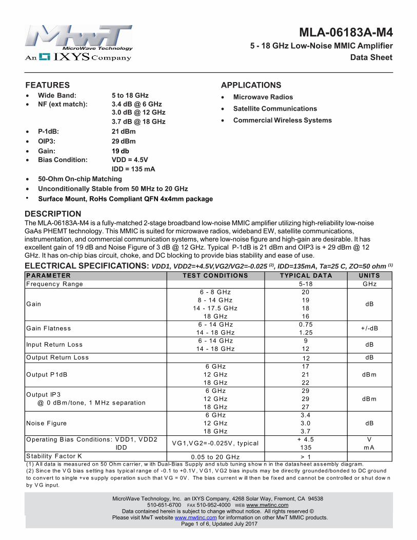
Recommended Application Board Design: Board Material is 10mil (Dielectric) thickness Rogers 4350B with 0.5oz cupper clads. Board is soldered on a gold plated solid cupper block and adequate heat-sinking is required for 1.5W total maximum power dissipation.
Part DescriptionC1, C2, C3, C4 0.1uF capacitor (0603)
MLA-06183A-M4 5 - 18 GHz Low-Noise MMIC Amplifier
Data Sheet
MicroWave Technology, Inc. an IXYS Company, 4268 Solar Way, Fremont, CA 94538 510-651-6700 FAX 510-952-4000 WEB www.mwtinc.com
Data contained herein is subject to change without notice. All rights reserved © Please visit MwT website www.mwtinc.com for information on other MwT MMIC products.
Page 6 of 6, Updated July 2017


![Appendix for test report method, the following formula should be taken to calculate it, ERP [dBm] = SGP [dBm] - Cable Loss [dB] + Gain [dBd] EIRP [dBm] = SGP [dBm] - Cable Loss [dB]](https://static.fdocuments.us/doc/165x107/5b1a153c7f8b9a1e258d424d/appendix-for-test-report-method-the-following-formula-should-be-taken-to-calculate.jpg)

![A 15 GHz Bandwidth 20 dBm PSAT Power Amplifier with ......-20 0 20 40 Frequency [GHz] dB] S21 S12 S11 S22 Large Signal Performances at 65GHz P SAT≈20dBm, P 1dB≈16dBm, PAE≈22%](https://static.fdocuments.us/doc/165x107/6125b92ca9a0936171190439/a-15-ghz-bandwidth-20-dbm-psat-power-amplifier-with-20-0-20-40-frequency.jpg)