4th Annual SFR Workshop & Review, April. 17, 2002
46
8:30 – 9:00 Research and Educational Objectives / Spanos 9:00 – 9:45 CMP / Doyle, Dornfeld, Talbot, Spanos 9:45 9:45 – 10:30 10:30 Plasma & Diffusion / Plasma & Diffusion / Graves, Lieberman, Cheung, Haller Graves, Lieberman, Cheung, Haller 10:30 – 10:45 break 10:45 – 12:00 Poster Session / Education, CMP, Plasma, Diffusion 12:00 – 1:00 lunch, / New Microlab Planning Update 1:00 – 1:45 Lithography / Spanos, Neureuther, Bokor 1:45 – 2:30 Sensors & Controls /Aydil, Poolla, Smith, Dunn, Cheung, Spanos 2:30 – 2:45 Break 2:45 – 4:30 Poster Session / all subjects 3:30 – 4:30 Steering Committee Meeting in room 606 Soda 4:30 – 5:30 Feedback Session 4th Annual SFR Workshop & Review, April. 17, 2002
Transcript of 4th Annual SFR Workshop & Review, April. 17, 2002

8:30 – 9:00 Research and Educational Objectives / Spanos
9:00 – 9:45 CMP / Doyle, Dornfeld, Talbot, Spanos
9:45 9:45 –– 10:30 10:30 Plasma & Diffusion / Plasma & Diffusion / Graves, Lieberman, Cheung, HallerGraves, Lieberman, Cheung, Haller
10:30 – 10:45 break10:45 – 12:00 Poster Session / Education, CMP, Plasma, Diffusion
12:00 – 1:00 lunch, / New Microlab Planning Update
1:00 – 1:45 Lithography / Spanos, Neureuther, Bokor
1:45 – 2:30 Sensors & Controls /Aydil, Poolla, Smith, Dunn, Cheung, Spanos
2:30 – 2:45 Break2:45 – 4:30 Poster Session / all subjects
3:30 – 4:30 Steering Committee Meeting in room 606 Soda4:30 – 5:30 Feedback Session
4th Annual SFR Workshop & Review, April. 17, 2002
4/17/2002 SFR Workshop - Plasma & Diffusion
2
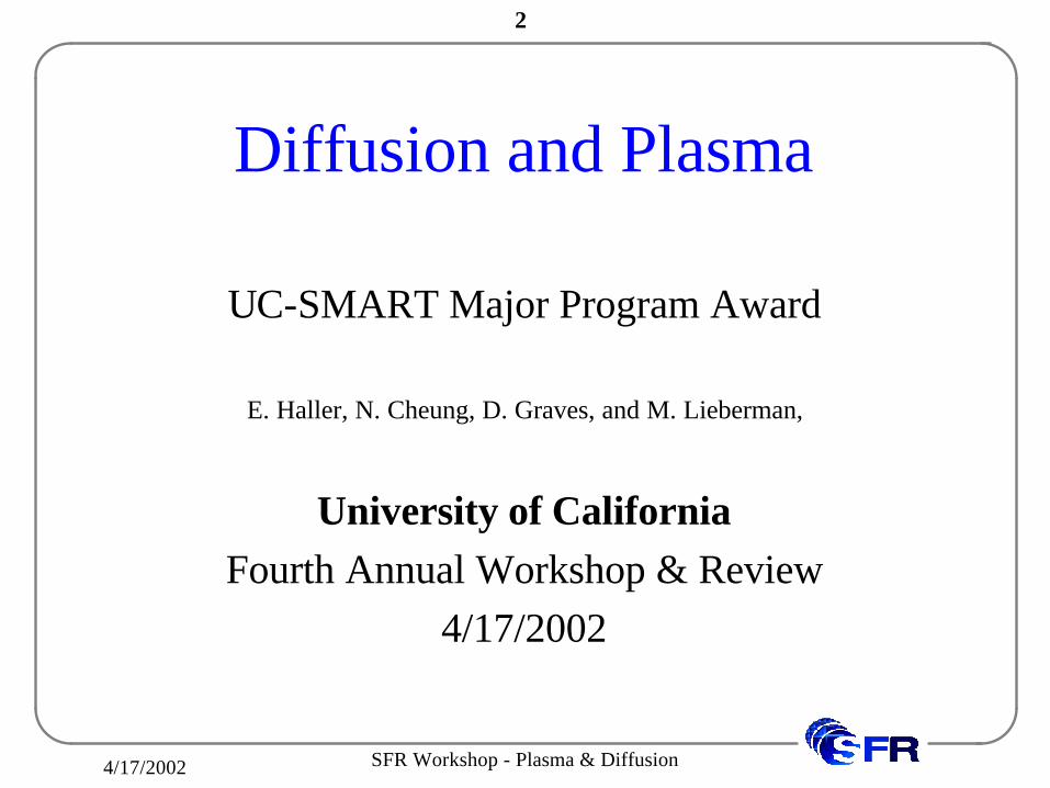
Diffusion and Plasma
UC-SMART Major Program Award
E. Haller, N. Cheung, D. Graves, and M. Lieberman,
University of CaliforniaFourth Annual Workshop & Review
4/17/2002

4/17/2002 SFR Workshop - Plasma & Diffusion
3
Fermi Level DependentDiffusion in Silicon
SMART/SFR Workshop and ReviewApril 17, 2002
Hughes Silvestri, Ian Sharp, Hartmut Bracht and Eugene E. Haller
University of California at Berkeley andLawrence Berkeley National Laboratory
Berkeley, CA 94720

4/17/2002 SFR Workshop - Plasma & Diffusion
4
Collaborators
• Hughes H. Silvestri, Graduate Student Research Assistant, MSE, UC Berkeley
• Ian D. Sharp, Undergraduate Student Research Assistant, Chem. Eng. & MSE, UC Berkeley
• Dr. Hartmut A. Bracht, Dept. of Materials Physics, University of Münster, Germany
• Dr. Steven Burden, ISONICS Corp., Golden, CO

4/17/2002 SFR Workshop - Plasma & Diffusion
5
Motivation• Downscaling of devices is, in part, limited by diffusion of dopants
(see: Paul Packan, Intel Corp., MRS San Francisco, April 19, 2001, Symposium X3, “Materials issues related to dopant diffusion and activation to form shallow, low resistance profiles will be addressed.”).
• Advanced modeling and control of diffusion requires an improved basic understanding of diffusion processes.
• Quantitative knowledge of the properties of silicon interstitials, one of the major active native defect assisting diffusion, is extremely limited. What are its charge states? Where do the energy levels lie in the silicon bandgap? What are the formation and migration energies? What are the individual contributions of the native defects to self-diffusion?

4/17/2002 SFR Workshop - Plasma & Diffusion
6
Approach
• Use undoped and doped Si isotope multilayer structures to study self- and dopant diffusion.
• Determine simultaneously the diffusivities of dopants and silicon as a function of temperature and Fermi level position.
• Major issue: Introduce dopants without causing transient phenomena (i.e., avoid “interstitial wind” caused by oxidation, implantation or clustering of excess dopant concentrations.)
• Use a low-temperature MBE-grown amorphous silicon cap layer, implanted at low energies as dopant diffusion source.
• Boron acceptor and Arsenic donor diffusion have been studied (see poster); Phosphorus diffusion is under investigation.

4/17/2002 SFR Workshop - Plasma & Diffusion
7
Experimental results: Boron as-implanted/Si isotope multilayer structure
1.0E+17
1.0E+18
1.0E+19
1.0E+20
1.0E+21
1.0E+22
1.0E+23
0 200 400 600 800 1000 1200 1400 1600 1800
depth (nm)
con
cen
trat
ion
(cm
-3)
B 30Si 28Si
28Si enriched layers
Natural Si layers
Artifact caused by SIMS etch pits
Amorphous Si layer
(260 nm)
Natural Si cap layer (200 nm)

4/17/2002 SFR Workshop - Plasma & Diffusion
8
Simultaneous diffusion of B and SiDiffusion anneal → SIMS → analysis: Bi
0 ⇔ Bs- + I 0,+ and
Bi0 + V 0,+ ⇔ Bs
-
1017
1018
1019
1020
1021
1022
0 600 1200 1800
30Si
B
depth (nm)
conc
entr
atio
n (c
m-3
)
T=950°C, t=15h+57 min
0.01
0.1
1
10
0 600 1200 1800
V +
V 0 I +
I 0
depth (nm)C
X /
Ceq x
B diffusion and doping favorsSi diffusion via I 0 and I + and suppresses Si diffusion via V

4/17/2002 SFR Workshop - Plasma & Diffusion
9
Temperature dependence of B and Si diffusion
10-20
10-18
10-16
10-14
10-12
10-10
0.6 0.7 0.8 0.9
1400 1200 1000 800
Bracht et al.(1998)
DSi(p)
DSi(ni)
DB
Antoniadis et al. (1978)
103/T (K-1)
D (
cm2 s-1
)
T (oC)
• B diffusion coefficients are consistent with literature data
• Si diffusion is enhanced under p-type doping and mainly controlled by I 0 and I +

4/17/2002 SFR Workshop - Plasma & Diffusion
10
Contribution of vacancies to Si self-diffusion?
1017
1018
1019
1020
1021
1022
0 500 1000 1500
30Si
As
depth (nm)
conc
entr
atio
n (c
m-3
)
as-implanted Si isotope structure
→ Diffusion of As in Si is known to be mediated both by I and V:
As implantation150 keV, 1016 cm-2
natSi (amorphous)
120 nm
natSi
28Si
1.3 µm
250 nm

4/17/2002 SFR Workshop - Plasma & Diffusion
11
Simultaneous diffusion of As and Si
1016
1018
1020
1022
0 500 1000 1500
V 2- V -
V 0
30Si
As
depth (nm)
conc
entra
tion
(cm
-3)
As diffusion: T=950°C, t=122h+14 min
Diffusion model: (AsV)0 ⇔ Ass+ + V - and (AsI)0 ⇔ Ass
+ + I 0
• As diffusion mediated by V - and I 0
• yields V - and I 0 contribution to DSi

4/17/2002 SFR Workshop - Plasma & Diffusion
12
Conclusion
• Boron diffusion via the kick-out mechanism Bi0 ⇔ Bs
- + I 0,+ ;interstitialcy mechanism1 ( [BI ]0 ⇔ Bs
- + I 0,+ ) not very likely; fBI ≤ 0.3
• Arsenic diffusion via vacancy and interstitialcy mechanism[AsV]0 ⇔ Ass
+ + V - and [AsI]0 ⇔ Ass+ + I 0 ; no V 0 and
V 2-
• I +, I 0, and V - contributions to Si diffusion add up accurately to DSi

4/17/2002 SFR Workshop - Plasma & Diffusion
13
Summary
• Boron diffusion in Si isotope structure is mediated by I+ and I0
– kick-out mechanism more likely than interstitialcy mechanism– native defect-controlled mode of B-diffusion– I+ and I0 contributions to Si self-diffusion– Q(I+) = 4.74 eV ; Q(I0) = 4.56 eV ; Q(B) = 3.56 eV
• Arsenic diffusion in Si isotope structure is proposed to be mediated by V - and I0
– interstitialcy and vacancy mechanisms both contribute– dopant defect-controlled mode of As diffusion– V - and I0 contributions to Si self-diffusion– Q(V -) = 5.18 eV ; Q(I0) = 4.32 eV ; Q(As) = 4.16 eV

4/17/2002 SFR Workshop - Plasma & Diffusion
14
Outlook and Future Work• As diffusion model is not unique concerning the defects V - and I0, i.e.,
fitting is also possible with I - and V0. Consequences: – only neutral vacancies? (in contradiction to our current understanding) – three charge states for self-interstitials? (further evidence for I - required)
• P diffusion studies in Si isotope structure are very important– P is considered to diffuse via the vacancy and the kick-out mechanism; native
defect-controlled mode of P diffusion– expect to distinguish between V - and I0 contributions to Si self-diffusion
• Upon completion of our studies, we will have comprehensive information about: detailed mechanisms of dopant diffusion (B, As, P, Sb); charge states of native point defects; individual contributions to Si self-diffusion
• Milestone 2002: Fermi level dependent diffusion studies with phosphorus and arsenic
• Milestone 2003: Dopant and self-diffusion in isotopically controlled SiGe structures (relaxed and strained)

4/17/2002 SFR Workshop - Plasma & Diffusion
15
Plasma Enhanced Bonding
SFR WorkshopApr 17, 2002
Yonah Cho and Nathan CheungBerkeley, CA
2002 GOAL: Enable wafer/die scale direct bonding of surfaces at low temperature (<200oC)

4/17/2002 SFR Workshop - Plasma & Diffusion
16
Problem Statement
..
Systems Integration
Enhanced Adhesion between low k /metal
Metal
polymerMetal
SOI Technology
Encapsulation of power sources
Plasma Enhanced Bonding Applications

4/17/2002 SFR Workshop - Plasma & Diffusion
17
State-of-the-ArtNo universal model on plasma assisted bonding mechanisms-Chemical force ?- Electrostatic force ?- Surface smoothing ?- Nano-plasticity of interfacial layer ?
Hydrophobic
Hydrophilic
3000
2500
2000
1500
1000
500
0100 200300400500 600700800 900
Surf
ace
Ene
rgy
(mJ/
m2 )
Annealing Temperature (oC)
OO22 plasmaplasmaTong et al.
APL 64, 625 (94)
UCBData

4/17/2002 SFR Workshop - Plasma & Diffusion
18
Our Approach
Bonding for a self-powered chip
Cross-section view
Power unit LED unit
Top view
a
b
a
b
Process flow:1. Si etch in KOH for wells2. Metal deposition for anode (-) & metal lift-off for patterning3. Metal bonding of LED ~200 oC4. Battery insertion5. Meta deposition for cathode (+) & patterning6. RT bonding of SiO2/Si7. Mechanical separation for top membrane
Si-undoped
SiO2

4/17/2002 SFR Workshop - Plasma & Diffusion
19
Low temperature encapsulation demonstration
SiO2, Si3N4 masks
Mask patterning
Si etch in KOHMask etch (SF6/He)
Piranha cleaning O2 plasma exposure
Bonding
InsertionPolymer film

4/17/2002 SFR Workshop - Plasma & Diffusion
20
Results/Justification for Approach
Demonstrated Low Temp Encapsulation: 25 oC- 150 oC
Infrared Transmission Image of Bonded Interface
3 cm
1.5 cm
1 cm 0.5 cm
Parafilm
Transparency
Cavity

4/17/2002 SFR Workshop - Plasma & Diffusion
21
New Approaches for low temperature Bonding
•Surface smoothing improves gap filling ability•Getters processing contaminants to form benign compounds at Si/BOX interface
F/Cl plasma or beam surface treatment
•Reduced surface Young’s modulus improves gap filling ability
Beam/Plasma implantation to modify nano-plasticity of surface layer
•Generation of silanol groups to increase surface bonding energy•H incorporation passivates oxide charge at Si/BOX interface
Water plasma treatment of Si-based surfaces

4/17/2002 SFR Workshop - Plasma & Diffusion
22
Justification for Approach Gap Closing Criterion for nm surface roughness
1x10 -8 1x10 -7 1x10 -6 1x10 -5 1x10⁻⁴ 1x10-310 -9
10 -8
10 -7
10 -6
10 -5
10 -4
10 -3
10 -2
10 -1
100
101
Op
en
ing
Ra
diu
s (c
m)
Height (cm)
R >2d
R < 2dGap opening
γ =10mJ/m2
R
2h d
γ =100mJ/m2
Gap closing
Wafer thickness = 0.5 mm
4/17/2002 SFR Workshop - Plasma & Diffusion
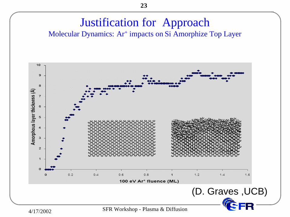
23
Justification for Approach Molecular Dynamics: Ar+ impacts on Si Amorphize Top Layer
(D. Graves ,UCB)
4/17/2002 SFR Workshop - Plasma & Diffusion
24
Plans
–– 20022002•• Hermetic testing of encapsulated battery with plasma Hermetic testing of encapsulated battery with plasma
bonding (with B. Dunn)bonding (with B. Dunn)•• Plasma and Ion Beam experiments to verify bonding Plasma and Ion Beam experiments to verify bonding
nanonano--plasticity andplasticity and silanolsilanol group mechanisms (with group mechanisms (with D. Graves)D. Graves)
–– 20032003• Bipolar Plasma Substrate Bias for enhanced
adhesion with polymer surfaces

4/17/2002 SFR Workshop - Plasma & Diffusion
25
SFR Workshop and ReviewApril 17, 2001Berkeley, CA
F. Greer, M. Nierode, M. Radtke, D. Fraser, J. Coburn and D. Graves Berkeley, CA
Plasma-Assisted Processes for Small Feature Reproducibility

4/17/2002 SFR Workshop - Plasma & Diffusion
26
Fundamental Beam Studies of Radical Enhanced Atomic Layer Deposition (RE-ALD)
• Barrier layers for interconnect must be very thin and highly conformal
• Atomic layer deposition (ALD) has been proposed for deposition of barrier films
• Our studies focus on the use of radicals for part of the atomic layer deposition process
• This offers the promise of greatly reduced deposition temperature
• Use of radicals for ALD must be characterized and understood

4/17/2002 SFR Workshop - Plasma & Diffusion
27
Progress and Research Activitiesü Conducted series of experiments demonstrating radical-enhanced
ALD and obtained fundamental kinetic parameters
ü Continued plasma testbed and model development for plasma processing of new materials
Since November
ü Studied adsorption kinetics of TiCl4 as a function of Tsurface and surface type
ü Demonstrated sub-monolayer precursor adsorption
ü Developed parameterized model of adsorption kinetics
ü Created FEMLAB-based model of non-isothermal, compressible neutral transport for plasma tool analysis
ü Installed new FTIR spectrometer on plasma experimental testbed

4/17/2002 SFR Workshop - Plasma & Diffusion
28
Milestones
• September 30th, 2001 ü Demonstrate TiN barrier layers deposited by novel ALD technology: REALCVD. Conduct preliminary film deposition studies. Test self-limiting film formation
• September 30th, 2002 üStudy effects of surface preparation, surface type and surface temperature on REALCVD film properties. Measurekey radical-surface kinetics. Project completion; student graduation.
• September 30th, 2003 Plasma processing of novel materials: experiments and modeling. Plasma and ion beam bonding experiments/models; (with N. Cheung)

4/17/2002 SFR Workshop - Plasma & Diffusion
29
Adsorption Issues in RE-ALD of TiN• RE-ALD1 uses a volatile metallic precursor and a radical source to deposit a film
• TiCl4/H/N Reactants introduced separately to achieve self-limiting growth
– Purpose is to grow film 1 monolayer at a time
• Film thickness controlled by repeating TiCl4/H/N cycles
• Nucleation regime observed by many authors
• Growth rate typically less than one monolayer/cycle even after nucleation regime
• Most studies done at higher temperatures > 200oC due kinetic constraints
1A. Sherman U.S. Patent 1999.
TiCl4Plasma (N/H)Ar
Time
Rea
ct. C
onc.
Film Thickness
Cycle Number
NucleationRegime ?

4/17/2002 SFR Workshop - Plasma & Diffusion
30
TiCl4 Precursor Adsorption
• Two distinct ads. regimes (Initial rapid followed by significantly slower)• Desorption of precursor à deposition rate/cycle lower at higher temperatures• Adsorption appears more uniform at higher temperatures • Adsorption likely submonolayer in all cases due to steric hinderance
*TiClx
TiCl4
Adsorption
*
TiCl4
0 2000 4000 6000 8000 10000
0.00E+000
2.00E+014
4.00E+014
6.00E+014
8.00E+014
1.00E+015
# of
TiC
l 2 Mol
ecul
es A
dsor
bed/
cm2
TiCl4 Exposure (1015 molecules/cm2)
Temp300K Temp350K Temp410K Temp445K
Submonolayer Adsorption
TiClx
Si QCM

4/17/2002 SFR Workshop - Plasma & Diffusion
31
Adsorption Model
*TiClx
*
TiCl4
TiClx
Desorption Diffusion
•Initial fraction of monolayer adsorbs due to line of sight collisions
• Subsequent adsorption proceeds through weakly bound intermediate species due to steric hinderance of TiCl2
•Increase in substrate temperature increases desorption more rapidly than diffusion1,2
•Two Site Model Fit to Data
• R = s1ΓTiCl4θ1+ s2ΓTiCl4θ2
–Sticking probabilities
–Active site (*) densities
• s2 = f(T)1Widdra, W. et al. Phys. Rev. Let. 74(11), 19952Kota, G.P.; Coburn, J.W.; Graves, D.B., J. Appl. Phys. 85(1), 1999.
0 4000 8000 12000 16000 20000
0.00E+000
2.00E+014
4.00E+014
6.00E+014
8.00E+014
1.00E+015
# of
TiC
l 2Mol
ecul
es A
dsor
bed/
cm2
TiCl4 Exposure (1015Molecules/cm
2)
Raw Adsorption Data (410K)Rapid Adsorption SitesSlow Adsorption SitesSum of Models
Unhindered sites rapidly filled by TiCl4
Hindered sites slowly filled (thermally activated)

4/17/2002 SFR Workshop - Plasma & Diffusion
32
0 100 200 300 400 500 600 700 800 900 1000-1.00E+014
0.00E+000
1.00E+014
2.00E+014
3.00E+014
4.00E+014
5.00E+014
6.00E+014
7.00E+014
8.00E+014
TiC
l 2 Mol
ecul
es A
dsor
bed
(#/c
m2 )
TiCl4 Exposure (1015 Molecules/cm2)
Silicon TiN W Cu
Adsorption on Different Surfaces
0
2E+15
4E+15
6E+15
8E+15
1E+16
1.2E+16
1.4E+16
0 1000 2000 3000 4000 5000Exposure (1015 TiCl4 Molecules/cm2s)
TiC
l 2m
olec
ules
/cm
2 Porous SilicaSample
Native Oxide
• Two regimes of adsorption not unique to Si surface
• Same qualitative behavior observed for TiN, W, Cu, and SiO2
• Porous material behaves much differently due to larger surface area

4/17/2002 SFR Workshop - Plasma & Diffusion
33
00.5
11.5
22.5
33.5
44.5
0 10 20 30 40
Dechlorination ResultsD
Cl
QCM
Dechlorination
• Residual Cl% can be controlled
through TiCl4 and D dosages
• Increasing relative D exposure time reduces Cl content to detection limit of XPS! (<0.3%)
• Comparable thermal ALD process
yields 1.5% Cl at 400oC1
•H recombination very important– γDH ~ 0.04 >> γDCl (3x10⁻⁴)–Much of D from plasma lost in ineffective channels
•N recombination difficult to measure in this system
– γNN ~ O(0.1)2
1 Satta, A. et al. MRS 2000 Spring Meeting (D6.5)
Residual Chlorine vs. Relative D Exposure
Cl C
onte
nt (%
)
Relative H or D Atom/Cl Exposure
Results for 30-100oC
D atoms (D2)H atoms (NH3)
2H. Singh, D.B. Graves, JAP 38 (6) 2000.

4/17/2002 SFR Workshop - Plasma & Diffusion
34
Conclusions: RE-ALD• RE-ALD processing questions
– Precursor (TiCl4)
• Adsorption is sub-monolayer over the range of surface T investigated
• Desorption of weakly bound TiCl4 precursor important in precursor adsorption
– Radicals (D,N)
• D radicals can reduce Cl content to < 0.3%
• N radicals likely can nitrogenate the substrate during first few cycles
• NH3 plasma results consistent with separate N and H fluxes

4/17/2002 SFR Workshop - Plasma & Diffusion
35
Future Plans
• Plasma processing of novel materials: experiments and plasma modeling.
•High k, low k, photoresist and metal gate materials
•Etch products, etch product interactions with surfaces
• Plasma and ion beam experiments to verify bonding nano-plasticity and silanol group mechanisms (with N. Cheung)
• Bipolar Plasma Substrate Bias for enhanced adhesion with polymer surfaces (with N. Cheung)

4/17/2002 SFR Workshop - Plasma & Diffusion
36
Plasma Sources for Small Feature Reproducibility
SFR WorkshopApril 17, 2002Berkeley, CA
M. A. Lieberman, A. J. Lichtenberg, A. M. MarakhtanovUC Berkeley, CA
P. Chabert (Ecole Polytechnique, France)M. Tuszewski (Los Alamos National Laboratory)

4/17/2002 SFR Workshop - Plasma & Diffusion
37
Milestones
• September 30, 2002- Characterize plasma instability using V-I-phase probe. - Model for reduced electron temperature and density.
• September 30, 2003- Develop and test instabilities control. Reduce electron
temperature and density in discharges.

4/17/2002 SFR Workshop - Plasma & Diffusion
38
Instabilities in Processing Plasmas
1 10 1000
200
400
600
800
1000
CAPACITIVE
INSTABILITY
INDUCTIVE
Abs
orbe
d P
ower
(W
)
Gas Pressure (mTorr)
1 10 1000
200
400
600
800
1000
INSTABILITY
CAPACITIVE
INDUCTIVE
Abs
orbe
d P
ower
(W
)Gas Pressure (mTorr)
Instability range in SF6 plasma Instability range in Ar/SF6 (1:1) plasma
Plasma instabilities have been observed in low pressure inductivedischarges with electronegative gas feedstocks (O2, SF6, etc)

4/17/2002 SFR Workshop - Plasma & Diffusion
39
Experiment (TCP)
QMS
PMT
∅ 30 cm
20 cm
GAS FEED
PUMP
Z-Scan V-I Probe
13.56 MHzPOWERSUPPLY
C1
C2
Planar Probe
Langmuir ProbeINDUCTIVE COIL

4/17/2002 SFR Workshop - Plasma & Diffusion
40
Ar/SF6 Plasma Parameters vs. Instability
0.0 0.5 1.0 1.5 2.00
1
2
3
4
5
6
7
8
9
10
Te
Ele
ctro
n T
empe
ratu
re T
e (e
V)
Time (ms)
0.0 0.5 1.0 1.5 2.01E7
1E8
1E9
1E10
ne
Ele
ctro
n de
nsity
ne (
cm-3)
Ar/SF6 (1:1) 5 mTorr, 350 W
Inductive mode (high density)
Capacitive mode (low density)
Instabilities occur in the transitionfrom capacitive (E) to inductive (H)mode of the discharge

4/17/2002 SFR Workshop - Plasma & Diffusion
41
Plasma Instabilities vs. Electron Power Absorption
Electron power absorptionper unit volume
+
++
= 20
202
nnnn
nnn
fRIPe
e
ce
ccindrfabs
capacitive inductive0 1
0
1
P ele
ctro
n/ V
olum
e
ne
capacitive inductive
Instability
Does reduction of capacitive coupling eliminate plasma instability?

4/17/2002 SFR Workshop - Plasma & Diffusion
42
Effect of Capacitive Coupling on Instability
Electrostatic (Faraday) Shield with Variable Area
Variable Faraday Shield§ up to 20 flat copper wedges§ shielded area: 0…100 %§ grounded
18°
TCP Coil

4/17/2002 SFR Workshop - Plasma & Diffusion
43
020
40
60
80 0100
200300
4000
4
8
12
16
Fre
quen
cy o
f Lig
ht, k
Hz
Power, W
Area covered
by shield , %
0 10 20 30 40 50 60 700
50
100150
200
250
300350
400STABLE INDUCTIVE
STABLE CAPACITIVE
UNSTABLE
Pow
er, W
Area covered by shield, %
Effect of Capacitive Coupling on Instability
§ Capacitive coupling and stable capacitive region reduced by Faraday shield§ Plasma instability continuously reduced by increase of the shielded area from
25 to 65 %§ Plasma relaxation oscillation frequencies decrease with shielded area increase § No instability observed for shielded area >65%
Ar/SF6 (1:1) 5 mTorr

4/17/2002 SFR Workshop - Plasma & Diffusion
44
Spatial Variations During Instability
0 1 2 3 4 50.0
0.4
0.8
1.2
1.6
20 mm 95 mm 170 mm
Pos
itive
ion
dens
ity (
a.u.
)
Time (ms)
170 mm
3 2 1
95 mm
20 mm
Probe @ -50 V
Ar/SF6 (1:1) 40 mTorr, 200 W
§ Spatial variations seen at higher pressures§ Instability decays more rapidly as pressure increases

4/17/2002 SFR Workshop - Plasma & Diffusion
45
Instabilities in Pure Inductive Discharges
0.000 0.001 0.002 0.003 0.004 0.005-3
-2
-1
0
1
2
3
Time (s)
Flo
atin
g pr
obe
pote
ntia
l (V
)
Ar/SF6 (1:1) 40 mTorr, 660 W
Instabilities have been observed in pure inductive discharges in Ar/SF6for pressures >20 mTorr (these fluctuations are small)

4/17/2002 SFR Workshop - Plasma & Diffusion
46
Future Work• Examine spatial variations during instability• Continue to study types of instabilities
a) Inductive to capacitive transition (kHz)b) Propagating inductive (kHz)c) Low frequency (Hz)d) Low pressure (< 3 mTorr)
• Continue to study capacitive coupling effect on instability• Continue to investigate the chemical composition of the discharge to
make improvements to the instability global model• Investigate instability effect on substrate
Publications1. M.A. Lieberman, A.J. Lichtenberg, and A.M. Marakhtanov, Instabilities in Low-pressure Inductive
Discharges with Attaching Gases, Appl. Phys. Lett. 75, 3617 (1999)2. P. Chabert, A.J. Lichtenberg, M.A. Lieberman, and A.M. Marakhtanov, Instabilities in Low-pressure
Electronegative Inductive Discharges, Plasma Sources Sci. Technol. 10, 478-489 (2001)