4A Sequencing LDO with Tracking and Ramp...
24
2017 Microchip Technology Inc. DS20005824A-page 1 MIC68400 Features • Stable with 10 μF Ceramic Capacitor • Input Voltage Range: 1.65V to 5.5V • 0.5V Reference • ±2.0% Output Tolerance over Temperature • 4A Maximum Output Current – Peak Start-Up • 3A Continuous Operating Current • Tracking on Turn-On and Turn-Off with Pin Strapping • Timing Controlled Sequencing On/Off • Programmable Ramp Control for In-Rush Current Limiting and Slew Rate Control of the Output Voltage During Turn-On and Turn-Off • Power-On Reset (POR) Supervisor with Programmable Delay Time • Single Master can Control Multiple Slave Regulators with Tracking Output Voltages • Tiny 4 mm x 4 mm QFN Package • Maximum Dropout (V IN – V OUT ) of 500 mV over Temperature at 3A Output Current • Fixed and Adjustable Output Voltages • Excellent Line and Load Regulation Specifications • Logic Controlled Shutdown • Thermal Shutdown and Current-Limit Protection Applications • FPGA/PLD Power Supply • Networking/Telecom Equipment • Microprocessor Core Voltage • High Efficiency Linear Post Regulator • Sequenced or Tracked Power Supply General Description The MIC68400 is a high peak current LDO regulator designed specifically for powering applications such as FPGA core voltages that require high start up current with lower nominal operating current. Capable of sourcing 4A of current for start-up, the MIC68400 provides high power from a small QFN leadless package. The MIC68400 can also implement a variety of power-up and power-down protocols such as sequencing, tracking, and ratiometric tracking. The MIC68400 operates from a wide input range of 1.65V to 5.5V, which includes all of the main supply voltages commonly available today. It is designed to drive digital circuits requiring low voltage at high currents (i.e. PLDs, DSP, microcontroller, etc.). The MIC68400 incorporates a delay pin (Delay) for control of power on reset output (POR) at turn-on and power-down delay at turn-off. In addition there is a ramp control pin (RC) for either tracking applications or output voltage slew rate adjustment at turn-on and turn-off. This is important in applications where the load is highly capacitive and in-rush currents can cause supply voltages to fail and microprocessors or other complex logic chips to hang up. Multiple MIC68400s can be daisy chained in two modes. In tracking mode the output voltage of the Master drives the RC pin of a Slave so that the Slave tracks the main regulator during turn-on and turn-off. In sequencing mode the POR of the Master drives the enable (EN) of the Slave so that it turns on after the Master and turns off before (or after) the Master. This behavior is critical for power-up and power-down control in multi-output power supplies. The MIC68400 is fully protected offering both thermal, current limit protection, and reverse current protection. The MIC68400 has a junction temperature range of –40°C to +125°C and is available in fixed as well as an adjustable option. The MIC68400 is offered in the tiny 16-pin 4 mm x 4 mm QFN package. 4A Sequencing LDO with Tracking and Ramp Control
Transcript of 4A Sequencing LDO with Tracking and Ramp...

2017 Microchip Technology Inc. DS20005824A-page 1
MIC68400
Features
• Stable with 10 µF Ceramic Capacitor
• Input Voltage Range: 1.65V to 5.5V
• 0.5V Reference
• ±2.0% Output Tolerance over Temperature
• 4A Maximum Output Current – Peak Start-Up
• 3A Continuous Operating Current
• Tracking on Turn-On and Turn-Off with Pin Strapping
• Timing Controlled Sequencing On/Off
• Programmable Ramp Control for In-Rush Current Limiting and Slew Rate Control of the Output Voltage During Turn-On and Turn-Off
• Power-On Reset (POR) Supervisor with Programmable Delay Time
• Single Master can Control Multiple Slave Regulators with Tracking Output Voltages
• Tiny 4 mm x 4 mm QFN Package
• Maximum Dropout (VIN – VOUT) of 500 mV over Temperature at 3A Output Current
• Fixed and Adjustable Output Voltages
• Excellent Line and Load Regulation Specifications
• Logic Controlled Shutdown
• Thermal Shutdown and Current-Limit Protection
Applications• FPGA/PLD Power Supply
• Networking/Telecom Equipment
• Microprocessor Core Voltage
• High Efficiency Linear Post Regulator
• Sequenced or Tracked Power Supply
General Description
The MIC68400 is a high peak current LDO regulatordesigned specifically for powering applications such asFPGA core voltages that require high start up currentwith lower nominal operating current. Capable ofsourcing 4A of current for start-up, the MIC68400provides high power from a small QFN leadlesspackage. The MIC68400 can also implement a varietyof power-up and power-down protocols such assequencing, tracking, and ratiometric tracking.
The MIC68400 operates from a wide input range of1.65V to 5.5V, which includes all of the main supplyvoltages commonly available today. It is designed todrive digital circuits requiring low voltage at highcurrents (i.e. PLDs, DSP, microcontroller, etc.). TheMIC68400 incorporates a delay pin (Delay) for controlof power on reset output (POR) at turn-on andpower-down delay at turn-off. In addition there is aramp control pin (RC) for either tracking applications oroutput voltage slew rate adjustment at turn-on andturn-off. This is important in applications where the loadis highly capacitive and in-rush currents can causesupply voltages to fail and microprocessors or othercomplex logic chips to hang up.
Multiple MIC68400s can be daisy chained in twomodes. In tracking mode the output voltage of theMaster drives the RC pin of a Slave so that the Slavetracks the main regulator during turn-on and turn-off. Insequencing mode the POR of the Master drives theenable (EN) of the Slave so that it turns on after theMaster and turns off before (or after) the Master. Thisbehavior is critical for power-up and power-downcontrol in multi-output power supplies. The MIC68400is fully protected offering both thermal, current limitprotection, and reverse current protection.
The MIC68400 has a junction temperature range of–40°C to +125°C and is available in fixed as well as anadjustable option. The MIC68400 is offered in the tiny16-pin 4 mm x 4 mm QFN package.
4A Sequencing LDO with Tracking and Ramp Control
MIC68400
DS20005824A-page 2 2017 Microchip Technology Inc.
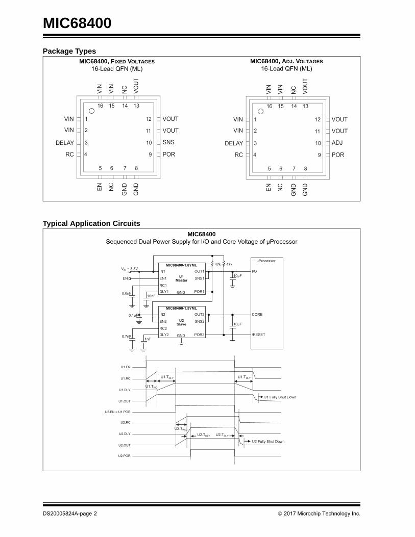
Package Types
Typical Application Circuits
MIC68400, FIXED VOLTAGES
16-Lead QFN (ML)MIC68400, ADJ. VOLTAGES
16-Lead QFN (ML)
13141516
12
11
10
9
1
2
3
4
8765
VIN
VIN
DELAY
RC
VOUT
VOUT
SNS
POR
VIN
VIN
NC VO
UT
EN NC
GN
D
GN
D
13141516
12
11
10
9
1
2
3
4
8765
VIN
VIN
DELAY
RC
VOUT
VOUT
ADJ
POR
VIN
VIN
NC VO
UT
EN NC
GN
D
GN
D
MIC68400Sequenced Dual Power Supply for I/O and Core Voltage of µProcessor
10μF
10μF
1nF
VIN = 3.3V
EN
IN1 OUT1
EN1 SNS1
RC1
DLY1 POR1
μProcessor
I/O
CORE
/RESET
47k 47k
10nF
0.7nF
0.6nF
MIC68400-1.8YML
U1Master
MIC68400-1.5YML
U2Slave
IN2 OUT2
EN2 SNS2
RC2
DLY2 GND
GND
POR2
0.1μF
U1.EN
U1.RC
U1.DLY
U1.OUT
U2.EN = U1.POR
U2.RC
U2.DLY
U2.OUT
U2.POR
U1.TRC
U2.TRC2
U1.TDLY U1.TDLY
U2.TDLY U2.TDLY
U1 Fully Shut Down
U2 Fully Shut Down
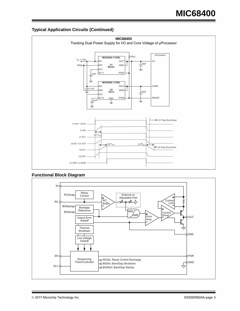
2017 Microchip Technology Inc. DS20005824A-page 3
MIC68400
Typical Application Circuits (Continued)
Functional Block Diagram
10μF
10μF
10nF
VIN = 1.8V
EN
IN1 OUT1
EN1
RC1
DLY1 POR1
μProcessor
I/O
CORE
/RESET
47k
10nF
MIC68400-1.8YML
U1Master
MIC68400-1.2YML
U2Slave
IN2 OUT2
EN2 SNS2
SNS1
RC2
DLY2 GND POR2
0.1μF
MIC68400Tracking Dual Power Supply for I/O and Core Voltage of µProcessor
U1.EN = U2.EN
U1.RC
U1.DLY
U2.RC = U1.OUT
U2.DLY
U2.OUT
U1.POR = U.2POR
U1.TRC
U2.TDLY U.2TDLY
U1 Fully Shut Down
U2 Fully Shut Down
BandgapReference
Output ErrorHoldoff
ThermalShutdown
Low VoltageHoldoff
SequencingTimer/Controller
BGStart
BGDis
RampControlRCDis
IN
RC
EN
DLY BGStart: BandGap StartupBGDis: BandGap ShutdownRCDis: Ramp Control Discharge
GND
POR
SNS
OUT
RCBuffer
ErrorAmp
CurrentDriver
CurrentLimit
External onAdjustable Part
AMPMIN

MIC68400
DS20005824A-page 4 2017 Microchip Technology Inc.
1.0 ELECTRICAL CHARACTERISTICS
Absolute Maximum Ratings †
Supply Voltage (VIN)....................................................................................................................................................+6VEnable Input Voltage (VEN) .........................................................................................................................................+6VPOR (VPOR) ..................................................................................................................................................... VIN + 0.3VRC .................................................................................................................................................................... VIN + 0.3VPower Dissipation (PD), (Note 1)............................................................................................................ Internally Limited
Operating Ratings ‡
Supply Voltage (VIN)................................................................................................................................ +1.65V to +5.5VEnable Input Voltage (VEN) ................................................................................................................................ 0V to VINRamp Control (VRC) ....................................................................................................................................... 0V to +5.5V
† Notice: Stresses above those listed under “Absolute Maximum Ratings” may cause permanent damage to the device.This is a stress rating only and functional operation of the device at those or any other conditions above those indicatedin the operational sections of this specification is not intended. Exposure to maximum rating conditions for extendedperiods may affect device reliability.
‡ Notice: The device is not guaranteed to function outside its operating ratings.
Note 1: The maximum allowable power dissipation of any TA (ambient temperature) is PD(MAX) = TJ(MAX) – TA)/θJA.Exceeding the maximum allowable power dissipation will result in excessive die temperature, and the reg-ulator will go into thermal shutdown.
TABLE 1-1: ELECTRICAL CHARACTERISTICS
Electrical Characteristics: TA = +25°C with VIN = VOUT + 1V; VEN = VIN; IOUT = 10 mA; bold values indicate –40°C ≤ TJ ≤ +125°C, unless noted. Note 1
Parameter Symbol Min. Typ. Max. Units Conditions
Output Voltage Accuracy –2 — 2 %10 mA < IOUT < IL(MAX), VOUT + 1 ≤ VIN ≤ 5.5V
Feedback Voltage VFB 0.49 0.50 0.51 V Adjustable version only
Feedback Current IFB — 20 — nA Adjustable version only
Output Voltage Line Regulation
— 0.06 0.5 % VIN = VOUT + 1V to 5.0V
Output Voltage Load Regulation
— 0.5 1 % IL = 10 mA to 3A
VIN – VO; Dropout Voltage
— — 400
mV
IL = 1.5A
— 300 500 IL = 3.0A
— 360 800 IL = 4.0A
Ground Pin Current IGND
— 1.2 —
mA
IL = 10 mA
— 20 — IL = 1.5A
— 55 — IL = 3.0A
— 90 130 IL = 4.0A
Shutdown Current ISHDN — 0.01 10 µA VEN = 0V; VOUT = 0V
Current Limit ILIMIT 4.0 6.0 — A VOUT = 0V; VIN = 3.0V
Start-Up Time tSU — 35 150 µs VEN = VIN; CRC = Open
Enable Input
Enable Input Threshold1 — —
VRegulator enable
— — 0.2 Regulator shutdown
Enable Hysteresis 20 120 200 mV —

2017 Microchip Technology Inc. DS20005824A-page 5
MIC68400
Enable Input Current— 0.02 —
µAVIL ≤ 0.2V (Regulator shutdown)
— 3 — VIH ≥ 1V (Regulator enable)
POR Output
POR Leakage Current IPOR(LEAK)— — 1
µA VPOR = 5.5V; POR = High— — 2
VPOR(LO) — 60 90 mVOutput Logic-Low Voltage (undervoltage condition), IPOR = 1 mA
VPOR
7.5 10 12.5
%
VOUT Ramping Up, Threshold, Percent of VOUT below nominal
10 12.5 15VOUT Ramping Down, Threshold, Percent of VOUT below nominal
— 3 — Hysteresis
Delay Current IDELAY 0.7 1 1.3 µA VDELAY = 0.75V
Delay Voltage (Note 2) VDELAY 1.185 1.235 1.285 V VPOR = High
Ramp Control
Ramp Control Current IRC 0.7 1 1.3 µA VRC = 0.75V
Output Discharge Current (Note 3)
IDC(OUT) 25 45 70 mA VOUT = 0.5VNOM, VRAMP =0V
Fixed Tracking Accuracy (Note 4)
–50 25 100 mV200 mV < VRC < VTARGET; Measure (VOUT – VRC)
Adjustable Tracking Accuracy (Note 4)
–10 15 50 mVMeasure (VOUT – VRC x (VTARGET/500 mV))
Note 1: Specification for packaged product only.
2: Timer High Voltage along with Delay pin current (1 µA nom.) determines the delay per µF of capacitance. Typical delay is 1.1 sec/µF.
3: Discharge current is the current drawn from the output to ground to actively discharge the output capacitor during the shutdown process.
4: VTARGET is the output voltage of an adjustable with customer resistor divider installed between VOUT and ADJ/SNS pin, or the rated output voltage of a fixed device.
TABLE 1-1: ELECTRICAL CHARACTERISTICS (CONTINUED)
Electrical Characteristics: TA = +25°C with VIN = VOUT + 1V; VEN = VIN; IOUT = 10 mA; bold values indicate –40°C ≤ TJ ≤ +125°C, unless noted. Note 1
Parameter Symbol Min. Typ. Max. Units Conditions
MIC68400
DS20005824A-page 6 2017 Microchip Technology Inc.
TEMPERATURE SPECIFICATIONS (Note 1)
Parameters Sym. Min. Typ. Max. Units Conditions
Temperature Ranges
Junction Temperature Range TJ –40 — +125 °C —
Storage Temperature Range TS –65 — +150 °C —
Package Thermal Resistances
Thermal Resistance 16-LD 4x4 QFN JA — 30 — °C/W —
Note 1: The maximum allowable power dissipation is a function of ambient temperature, the maximum allowable junction temperature and the thermal resistance from junction to air (i.e., TA, TJ, JA). Exceeding the maximum allowable power dissipation will cause the device operating junction temperature to exceed the maximum +125°C rating. Sustained junction temperatures above +125°C can impact the device reliability.

2017 Microchip Technology Inc. DS20005824A-page 7
MIC68400
2.0 TYPICAL PERFORMANCE CURVES
FIGURE 2-1: Dropout Voltage vs. Temperature.
FIGURE 2-2: Output Voltage vs. Input Voltage.
FIGURE 2-3: Ground Current vs. Output Current.
FIGURE 2-4: Dropout Voltage vs. Output Current.
FIGURE 2-5: Current Limit vs. Input Voltage.
FIGURE 2-6: Enable Threshold vs. Input Voltage.
Note: The graphs and tables provided following this note are a statistical summary based on a limited number ofsamples and are provided for informational purposes only. The performance characteristics listed hereinare not tested or guaranteed. In some graphs or tables, the data presented may be outside the specifiedoperating range (e.g., outside specified power supply range) and therefore outside the warranted range.

MIC68400
DS20005824A-page 8 2017 Microchip Technology Inc.
FIGURE 2-7: Ground Current vs. Input Voltage.
FIGURE 2-8: Output Voltage vs. Temperature.
FIGURE 2-9: Ground Current vs. Temperature.
FIGURE 2-10: Power Supply Rejection Ratio.
FIGURE 2-11: Load Regulation.
FIGURE 2-12: Thermal Shutdown.
2017 Microchip Technology Inc. DS20005824A-page 9
MIC68400
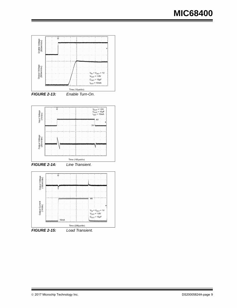
FIGURE 2-13: Enable Turn-On.
FIGURE 2-14: Line Transient.
FIGURE 2-15: Load Transient.

MIC68400
DS20005824A-page 10 2017 Microchip Technology Inc.
3.0 PIN DESCRIPTIONS
The descriptions of the pins are listed in Table 3-1.
TABLE 3-1: PIN FUNCTION TABLE
Pin Number Pin Name Description
1, 2, 15, 16 VIN Input: Input voltage supply pin. Place a capacitor to ground to bypass the input supply.
3 DELAY Delay: Capacitor to ground sets internal delay timer. Timer delays power-on reset (POR) output at turn-on, and ramp down at turn-off.
4 RC Ramp Control: May be voltage driven for tracking applications or a capacitor to ground will set the slew rate of output voltage during start-up.
5 EN Enable (Input): CMOS compatible input. Logic-high = enable, logic-low = shutdown.
6, 14 NC Not internally connected.
7, 8, Tab GND Ground.
9 POR Power-on Reset: Open-drain output device indicates when the output is in regulation. High (open) means device is regulating within 10%. POR onset can be delayed using a single capacitor from Delay to ground.
10 (Fixed) SNS Output Voltage Sense Pin: Connect directly to output pin.
10 (Adj.) ADJ Adjustable regulators: Feedback input. Connect to resistor voltage divider.
11, 12, 13 VOUT Output Voltage: Output of voltage regulator. Place capacitor to ground to bypass the output voltage. Minimum load current is 100 µA. Nominal bypass capacitor is 10 µF.
2017 Microchip Technology Inc. DS20005824A-page 11
MIC68400
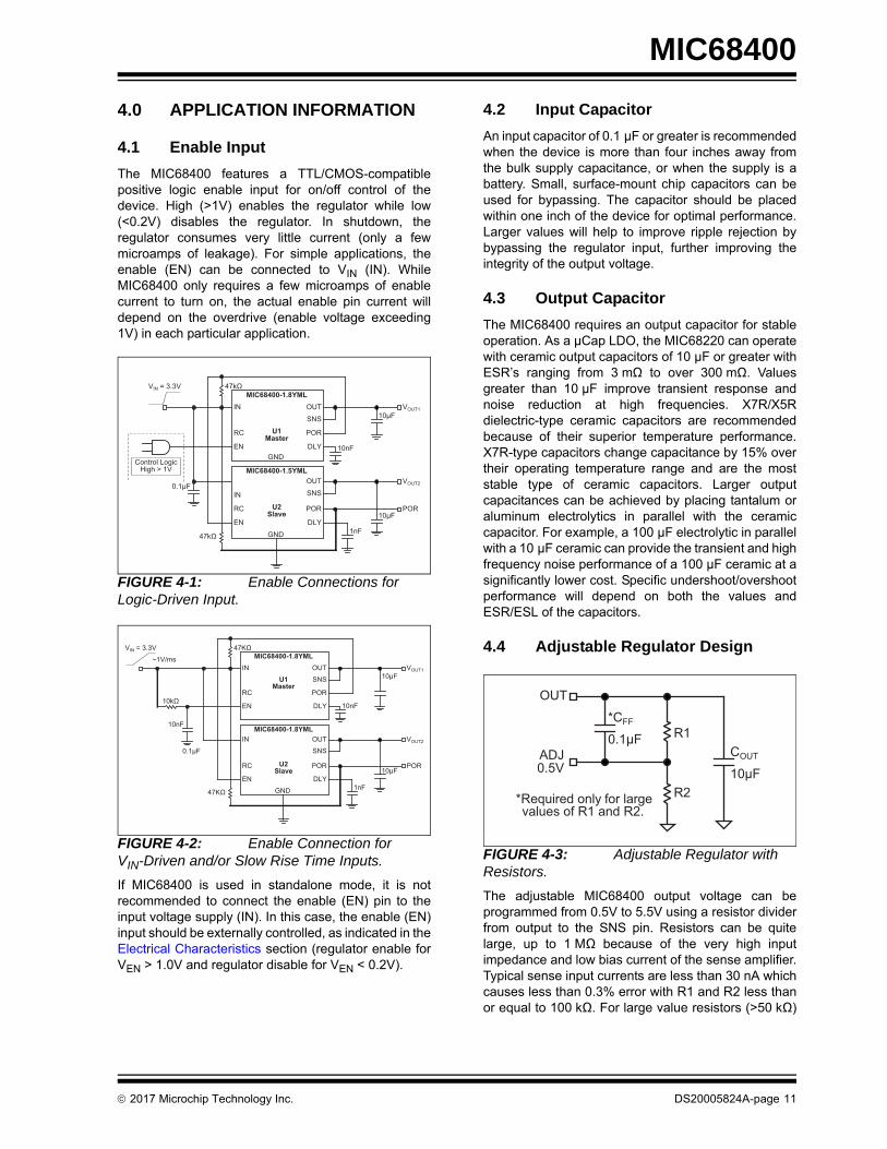
4.0 APPLICATION INFORMATION
4.1 Enable Input
The MIC68400 features a TTL/CMOS-compatiblepositive logic enable input for on/off control of thedevice. High (>1V) enables the regulator while low(<0.2V) disables the regulator. In shutdown, theregulator consumes very little current (only a fewmicroamps of leakage). For simple applications, theenable (EN) can be connected to VIN (IN). WhileMIC68400 only requires a few microamps of enablecurrent to turn on, the actual enable pin current willdepend on the overdrive (enable voltage exceeding1V) in each particular application.
FIGURE 4-1: Enable Connections for Logic-Driven Input.
FIGURE 4-2: Enable Connection for VIN-Driven and/or Slow Rise Time Inputs.
If MIC68400 is used in standalone mode, it is notrecommended to connect the enable (EN) pin to theinput voltage supply (IN). In this case, the enable (EN)input should be externally controlled, as indicated in theElectrical Characteristics section (regulator enable forVEN > 1.0V and regulator disable for VEN < 0.2V).
4.2 Input Capacitor
An input capacitor of 0.1 µF or greater is recommendedwhen the device is more than four inches away fromthe bulk supply capacitance, or when the supply is abattery. Small, surface-mount chip capacitors can beused for bypassing. The capacitor should be placedwithin one inch of the device for optimal performance.Larger values will help to improve ripple rejection bybypassing the regulator input, further improving theintegrity of the output voltage.
4.3 Output Capacitor
The MIC68400 requires an output capacitor for stableoperation. As a µCap LDO, the MIC68220 can operatewith ceramic output capacitors of 10 µF or greater withESR’s ranging from 3 mΩ to over 300 mΩ. Valuesgreater than 10 µF improve transient response andnoise reduction at high frequencies. X7R/X5Rdielectric-type ceramic capacitors are recommendedbecause of their superior temperature performance.X7R-type capacitors change capacitance by 15% overtheir operating temperature range and are the moststable type of ceramic capacitors. Larger outputcapacitances can be achieved by placing tantalum oraluminum electrolytics in parallel with the ceramiccapacitor. For example, a 100 µF electrolytic in parallelwith a 10 µF ceramic can provide the transient and highfrequency noise performance of a 100 µF ceramic at asignificantly lower cost. Specific undershoot/overshootperformance will depend on both the values andESR/ESL of the capacitors.
4.4 Adjustable Regulator Design
FIGURE 4-3: Adjustable Regulator with Resistors.
The adjustable MIC68400 output voltage can beprogrammed from 0.5V to 5.5V using a resistor dividerfrom output to the SNS pin. Resistors can be quitelarge, up to 1 MΩ because of the very high inputimpedance and low bias current of the sense amplifier.Typical sense input currents are less than 30 nA whichcauses less than 0.3% error with R1 and R2 less thanor equal to 100 kΩ. For large value resistors (>50 kΩ)
VOUT2
POR
1nF
VIN = 3.3V
IN OUT
RC POR
SNS
EN DLY
47MIC68400-1.8YML
U1Master
MIC68400-1.5YML
U2Slave
IN SNS
OUT
RC POR
EN
GND
GND
DLY
0.1μF
10μF
10nF
47
Control LogicHigh > 1V
10μFVOUT1
10μF
1nF
VIN = 3.3V
~1V/msIN OUT
SNS
RC POR
EN DLY
47MIC68400-1.8YML
U1Master
MIC68400-1.8YML
U2Slave
IN OUT
SNS
RC POR
EN
GND
DLY
10nF
0.1μF
10μF
10nF
47
VOUT1
VOUT2
POR
R1
OUT
ADJ0.5V
R2
COUT
10μF
*CFF
0.1μF
*Required only for large values of R1 and R2.
MIC68400
DS20005824A-page 12 2017 Microchip Technology Inc.
R1 should be bypassed by a small capacitor (CFF =0.1 µF bypass capacitor) to avoid instability due tophase lag at the ADJ/SNS input.
The output resistor divider values are calculated by:
EQUATION 4-1:
4.5 Power on Reset (POR) and Delay (DLY)
The power-on reset output (POR) is an open-drainN-Channel device requiring a pull-up resistor to eitherthe input voltage or output voltage for proper voltagelevels. POR is driven by the internal timer so that therelease of POR at turn-on can be delayed for as muchas one second. POR is always pulled low when enable(EN) is pulled low or the output goes out of regulationby more than 10% due to loading conditions.
The internal timer is controlled by the DLY pin whichhas a bidirectional current source and two limitingcomparators. A capacitor connected from DLY to GNDsets the delay time for two functions. On start up, DLYsets the time from the nominal output voltage isreached to the release of the POR. At shut down, thedelay sets the time from disable (EN pin driven low) toactual ramp down of the output voltage. The currentsource is ±1 µA, which charges the capacitor from~150 mV (nominal disabled DLY voltage) to ~1.25V. Atturn on, the DLY cap begins to charge when the outputvoltage reaches 90% of the target value. When thecapacitor reaches 1.25V, the output of the POR isreleased to go high. At turn off, the DLY cap begins todischarge when the EN is driven low. When the capreaches ~150 mV the output is ramped down. Bothdelays are nominally the same, and are calculated bythe same formula:
EQUATION 4-2:
The scale factor is 1.1 seconds/µF, 1.1 ms/nF, or1.1 µs/pF. tDLYOFF is the time from lowering of EN to thestart of ramp down on the off cycle. TPOR is the timefrom the rising of EN to the release (low to high edge)of the POR. This behavior means that a µProcessor orother complex logic system is guaranteed that the
nominal output voltage is stable for a known timebefore the POR is released, and they are furtherguaranteed that once POR is pulled low, they have aknown time to ‘tidy up’ memory or other registers for awell-controlled shutdown. In Master/Slaveconfigurations, the timers can be used to ensure thatthe Master is always accurately regulating when theSlave is on.
4.6 Ramp Control
The ramp control (RC) has a bidirectional currentsource and a sense amplifier, which together are usedto control the voltage at the output. When RC is belowthe target voltage (nominal output voltage for fixedvoltage parts, 0.5V for adjustable parts) the RC pincontrols the output voltage. When RC is at or above thetarget voltage, the output is controlled by the internalregulator.
4.6.1 TRACKING APPLICATIONS: DRIVING RC FROM A VOLTAGE SOURCE
Fixed Parts: If RC is driven from another (Master)regulator the two outputs will track each other until theMaster exceeds the target voltage of the Slaveregulator. Typically the output of the MIC68400 willtrack above the RC input by 30 mV to 70 mV. Thisoffset is designed to allow Master/Slave tracking ofsame-voltage regulators. Without the offset,same-voltage Master/Slave configurations could sufferpoor regulation.
Adjustable Parts: The RC pin on adjustable versionsoperates from 0V to 0.5V. To implement tracking on anadjustable version, an external resistor divider must beused. This divider is the nearly same ratio as thevoltage setting divider used to drive the SNS/ADJ pin.It is recommended that the ratio be adjusted to track~50 mV (2% to 3%) above the target voltage if theMaster and Slave are operating at the same targetvoltage.
4.6.2 RAMP UP: CAP-CONTROLLED SLEW RATE
If a capacitor is connected to RC, the bidirectionalcurrent source will charge the cap during startup anddischarge the cap during shutdown. The size of thecapacitor and the RC current (1 µA nom.) control theslew rate of the output voltage during startup. Forexample, to ramp up a 1.8V regulator from zero to fulloutput in 10 ms requires a 5.6 nF capacitor.
VOUT 0.5V R1R2------- 1+ =
tDLY 1.1 CDLY
1A------------- =

2017 Microchip Technology Inc. DS20005824A-page 13
MIC68400
For Fixed Versions:
EQUATION 4-3:
Similarly, to slew an adjustable (any output voltage)from zero to full output in 10 ms requires a 20 nF cap.
For Adjustable Versions:
EQUATION 4-4:
4.6.3 RAMP DOWN: TURN OFF SLEW RATE
When EN is lowered and the DLY pin has discharged,the RC pin and the OUT pin slew toward zero. For fixedvoltage devices, the RC pin slew rate is 2 to 3 times theSRON defined above. For adjustable voltage devices,the RC pin slew is much higher. In both cases, turn offslew rate may be determined by the RC pin for lowvalues of output capacitor, or by the maximumdischarge current available at the output for largevalues of output capacitor. Turn off slew rate is not aspecified characteristic of the MIC68400.
4.7 Sequencing Configurations
Sequencing refers to timing-based Master/Slavecontrol between regulators. It allows a Master device tocontrol the start and stop timing of a single or multipleSlave devices. In typical sequencing the Master PORdrives the Slave EN. The sequence begins with theMaster EN driven high. The Master output ramps upand triggers the Master DLY when the Master outputreaches 90%. The Master DLY then determines whenthe POR is released to enable the Slave device. Whenthe Master EN is driven low, the Master POR isimmediately pulled low causing the Slave to rampdown. However, the Master output will not ramp downuntil the Master DLY has fully discharged. In this way,the Master power can remain good after the Slave hasbeen ramped down.
In sequencing configurations the Master DLY controlsthe turn-on time of the Slave and the Slave DLYcontrols the turn-off time of the Slave.
FIGURE 4-4: Sequencing Connections.
In the figure below, CDLYS > CDLYM. CDLYS = 2 nF,CDLYM = 1 nF.
FIGURE 4-5: Delayed Sequencing.
In the figure below, CDLYS < CDLYM. CDLYS = 1 nF,CDLYM = 2 nF.
FIGURE 4-6: Windowed Sequencing.
4.8 Tracking Configurations
4.8.1 NORMAL TRACKING
In normal tracking, the Slave RC pin is driven from theMaster output. The internal control buffering ensuresthat the output of the Slave is always slightly above theMaster to guarantee that the Slave properly regulates
tRC VOUT
CRC
1A---------- = SRON
1ACRC---------- =
tRC 0.5VCRC
1A---------- = SRON 2VOUT
1ACRC---------- =
4.7μF
CDLY2
VIN = 3.3V
EN
IN1OUT1SNS1
RC1 POR1
EN1 DLY1
MIC68400
IN2
OUT2
SNS2
RC2 POR2
EN2
GND
DLY24.7μF
0.1μF
CDLY1
μProcessor
I/O
CORE
/RESET

MIC68400
DS20005824A-page 14 2017 Microchip Technology Inc.
(based on its own internal reference) if Master andSlave are both fixed voltage devices of the same outputvoltage. The schematic and plot below show a 1.2Vdevice tracking a 1.8V device through the entireturn-on/turn-off sequence. Note that because the RCpin will overdrive the target voltage (to ensure properregulation), the ramp down delay is longer than thePOR delay during turn-on.
FIGURE 4-7: Fixed Voltage Devices.
Fixed voltage versions of MIC68400 have two internalvoltage dividers: one for setting the output voltage andthe other for driving the tracking circuitry. Adjustableparts have up to two external dividers: one from outputto SNS (to set the output voltage) and one from theoutput to the Slave RC pin (in tracking configurations).Also, the RC pin in fixed parts operates at the samevoltage as the output, whereas the RC pin in adjustableparts operates at the 0.5V reference. To set up anormal tracking configuration, the divider driving theSlave RC pin is the same ratio (or nearly the same – ifboth Master and Slave are set to the same outputvoltage, the Slave RC divider should be adjusted 2% to4% higher) as the divider driving the Slave SNS pin.This is shown in Figure 4-8.
FIGURE 4-8: Adjustable Voltage Devices.
10μF
10μF
VIN = 2.5V
EN
IN OUT
EN SNS
RC
DLY POR
VOUT1
VOUT2
POR
1nF1nF
MIC68400-1.2YML
U2Slave
MIC68400-1.8YML
U1Master
IN OUT
EN SNS
RC
DLY
GND
PORNC
0.1μF
10μF
10μF
VIN = 3.3V
EN
IN OUT
EN
RC
DLY POR
VOUT1
VOUT2
POR
1nF2nF
MIC68400YML
U1Master
MIC68400YML
U2Slave
IN OUT
EN
RC
DLY
GND
PORNC
0.1μF
ADJ
ADJ

2017 Microchip Technology Inc. DS20005824A-page 15
MIC68400
4.8.2 RATIOMETRIC TRACKING
Ratiometric tracking allows independent rampingspeeds for both regulators so that the regulationvoltage is reached at the same time. This isaccomplished by adding a resistor divider between theMaster output pin and the Slave RC pin. The dividershould be scaled such that the Slave RC pin reachesor exceeds the target output voltage of the Slave as theMaster reaches its target voltage.
FIGURE 4-9: Fixed Voltage Devices.
Ratiometric tracking may be used with adjustable partsby simply connecting the RC pins of the Master andSlave. Use a single RC capacitor of twice the normalvalue (because twice the current is injected into thesingle RC cap). Alternatively, fixed parts may useratiometric tracking in a manner similar to adjustablenormal tracking, with the tracking divider changed tothe same resistor ratio driving the Master ADJ/SNS pin.
FIGURE 4-10: Adjustable Voltage Devices.
4.9 Final Note on Tracking
The MIC68400 does not fully shut down until the outputload is discharged to near zero. If RC is driven from anexternal source in a tracking configuration, and theexternal source does not go to zero on shutdown, itmay prevent complete shutdown of the MIC68400. Thiswill cause no damage, but some Q current will remainand may cause concern in battery operated portableequipment. Also, when RC is driven in tracking mode,pulling EN low will not cause the output to drop.Maintaining low EN in tracking mode simply means thatthe MIC68400 will shutdown when the tracking voltagegets near zero. In no case can the MIC68400 enter thetracking mode unless EN is pulled high.
10μF
10μF
VIN = 3.3V
EN
IN OUT
EN SNS
RC
DLY POR
VOUT1
VOUT2
POR
1nF1nF
MIC68400-1.2YML
U2Slave
MIC68400-1.8YML
U1Master
IN OUT
EN SNS
RC
DLY GND
GND
PORNC
0.1μF
10μF
10μF
VIN = 3.3V
EN
IN OUT
EN
RC
DLY POR
VOUT1
VOUT2
POR
1nF3nF
MIC68400YML
U2Slave
U1Master
MIC68400YML
IN OUT
EN
RC
DLY GND
GND
PORNC
0.1μF
ADJ
ADJ

MIC68400
DS20005824A-page 16 2017 Microchip Technology Inc.
5.0 PACKAGING INFORMATION
5.1 Package Marking Information
Example
X.XXXXXXXXX-
16-Lead QFN*(Fixed)
Example16-Lead QFN*(Adjustable)
WNNN1.2YML68400-
6026
XXXXXXXX
WNNNYML68400
2943
Legend: XX...X Product code or customer-specific informationY Year code (last digit of calendar year)YY Year code (last 2 digits of calendar year)WW Week code (week of January 1 is week ‘01’)NNN Alphanumeric traceability code Pb-free JEDEC® designator for Matte Tin (Sn)* This package is Pb-free. The Pb-free JEDEC designator ( )
can be found on the outer packaging for this package.
, , Pin one index is identified by a dot, delta up, or delta down (trianglemark).
Note: In the event the full Microchip part number cannot be marked on one line, it willbe carried over to the next line, thus limiting the number of availablecharacters for customer-specific information. Package may or may not includethe corporate logo.
Underbar (_) and/or Overbar (⎯) symbol may not be to scale.
3e
3e

2017 Microchip Technology Inc. DS20005824A-page 17
MIC68400
16-Lead 4 mm x 4 mm QFN Package Outline and Recommended Land Pattern
Note: For the most current package drawings, please see the Microchip Packaging Specification located at http://www.microchip.com/packaging.

MIC68400
DS20005824A-page 18 2017 Microchip Technology Inc.
NOTES:

2017 Microchip Technology Inc. DS20005824A-page 19
MIC68400
APPENDIX A: REVISION HISTORY
Revision A (August 2017)
• Converted Micrel document MIC68400 to Micro-chip data sheet DS20005824A.
• Minor text changes throughout.
• Paragraph added after Figure 4-2 in Section 4.2 “Input Capacitor”.

MIC68400
DS20005824A-page 20 2017 Microchip Technology Inc.

2017 Microchip Technology Inc. DS20005824A-page 21
MIC68400
PRODUCT IDENTIFICATION SYSTEM
To order or obtain information, e.g., on pricing or delivery, contact your local Microchip representative or sales office.
Examples:
a) MIC68400-1.2YML-TR: 4A Sequencing LDO with Tracking and Ramp Control,1.2V, –40°C to +125°C, 16-Lead QFN, 5,000/Reel
b) MIC68400-1.8YML-TR: 4A Sequencing LDO with,Tracking and Ramp Control1.8V, –40°C to +125°C, 16-Lead QFN, 5,000/Reel
c) MIC68400YML-TR: 4A Sequencing LDO with,Tracking and Ramp ControlAdjustable Voltage, –40°C to +125°C, 16-LeadQFN, 5,000/Reel
PART NO. XX
PackageDevice
Device: MIC68400: 4A Sequencing LDO with Tracking and Ramp Control
Voltage: 1.2 = 1.2V1.8 = 1.8Vblank= Adjustable
Temperature: Y = –40°C to +125°C
Package: ML = 16-Lead 4 mm x 4 mm QFN
Media Type: TR = 5,000/Reel
–X.X
Voltage
X
Temperature
Note 1: Tape and Reel identifier only appears in the catalog part number description. This identifier is used for ordering purposes and is not printed on the device package. Check with your Microchip Sales Office for package availability with the Tape and Reel option.
–XX
Media Type

MIC68400
DS20005824A-page 22 2017 Microchip Technology Inc.
NOTES:

2017 Microchip Technology Inc. DS20005824A-page 23
Information contained in this publication regarding deviceapplications and the like is provided only for your convenienceand may be superseded by updates. It is your responsibility toensure that your application meets with your specifications.MICROCHIP MAKES NO REPRESENTATIONS ORWARRANTIES OF ANY KIND WHETHER EXPRESS ORIMPLIED, WRITTEN OR ORAL, STATUTORY OROTHERWISE, RELATED TO THE INFORMATION,INCLUDING BUT NOT LIMITED TO ITS CONDITION,QUALITY, PERFORMANCE, MERCHANTABILITY ORFITNESS FOR PURPOSE. Microchip disclaims all liabilityarising from this information and its use. Use of Microchipdevices in life support and/or safety applications is entirely atthe buyer’s risk, and the buyer agrees to defend, indemnify andhold harmless Microchip from any and all damages, claims,suits, or expenses resulting from such use. No licenses areconveyed, implicitly or otherwise, under any Microchipintellectual property rights unless otherwise stated.
Trademarks
The Microchip name and logo, the Microchip logo, AnyRate, AVR, AVR logo, AVR Freaks, BeaconThings, BitCloud, CryptoMemory, CryptoRF, dsPIC, FlashFlex, flexPWR, Heldo, JukeBlox, KEELOQ, KEELOQ logo, Kleer, LANCheck, LINK MD, maXStylus, maXTouch, MediaLB, megaAVR, MOST, MOST logo, MPLAB, OptoLyzer, PIC, picoPower, PICSTART, PIC32 logo, Prochip Designer, QTouch, RightTouch, SAM-BA, SpyNIC, SST, SST Logo, SuperFlash, tinyAVR, UNI/O, and XMEGA are registered trademarks of Microchip Technology Incorporated in the U.S.A. and other countries.
ClockWorks, The Embedded Control Solutions Company, EtherSynch, Hyper Speed Control, HyperLight Load, IntelliMOS, mTouch, Precision Edge, and Quiet-Wire are registered trademarks of Microchip Technology Incorporated in the U.S.A.
Adjacent Key Suppression, AKS, Analog-for-the-Digital Age, Any Capacitor, AnyIn, AnyOut, BodyCom, chipKIT, chipKIT logo, CodeGuard, CryptoAuthentication, CryptoCompanion, CryptoController, dsPICDEM, dsPICDEM.net, Dynamic Average Matching, DAM, ECAN, EtherGREEN, In-Circuit Serial Programming, ICSP, Inter-Chip Connectivity, JitterBlocker, KleerNet, KleerNet logo, Mindi, MiWi, motorBench, MPASM, MPF, MPLAB Certified logo, MPLIB, MPLINK, MultiTRAK, NetDetach, Omniscient Code Generation, PICDEM, PICDEM.net, PICkit, PICtail, PureSilicon, QMatrix, RightTouch logo, REAL ICE, Ripple Blocker, SAM-ICE, Serial Quad I/O, SMART-I.S., SQI, SuperSwitcher, SuperSwitcher II, Total Endurance, TSHARC, USBCheck, VariSense, ViewSpan, WiperLock, Wireless DNA, and ZENA are trademarks of Microchip Technology Incorporated in the U.S.A. and other countries.
SQTP is a service mark of Microchip Technology Incorporated in the U.S.A.
Silicon Storage Technology is a registered trademark of Microchip Technology Inc. in other countries.
GestIC is a registered trademark of Microchip Technology Germany II GmbH & Co. KG, a subsidiary of Microchip Technology Inc., in other countries.
All other trademarks mentioned herein are property of their respective companies.
© 2017, Microchip Technology Incorporated, All Rights Reserved.
ISBN: 978-1-5224-2075-0
Note the following details of the code protection feature on Microchip devices:
• Microchip products meet the specification contained in their particular Microchip Data Sheet.
• Microchip believes that its family of products is one of the most secure families of its kind on the market today, when used in the intended manner and under normal conditions.
• There are dishonest and possibly illegal methods used to breach the code protection feature. All of these methods, to our knowledge, require using the Microchip products in a manner outside the operating specifications contained in Microchip’s Data Sheets. Most likely, the person doing so is engaged in theft of intellectual property.
• Microchip is willing to work with the customer who is concerned about the integrity of their code.
• Neither Microchip nor any other semiconductor manufacturer can guarantee the security of their code. Code protection does not mean that we are guaranteeing the product as “unbreakable.”
Code protection is constantly evolving. We at Microchip are committed to continuously improving the code protection features of ourproducts. Attempts to break Microchip’s code protection feature may be a violation of the Digital Millennium Copyright Act. If such actsallow unauthorized access to your software or other copyrighted work, you may have a right to sue for relief under that Act.
Microchip received ISO/TS-16949:2009 certification for its worldwide headquarters, design and wafer fabrication facilities in Chandler and Tempe, Arizona; Gresham, Oregon and design centers in California and India. The Company’s quality system processes and procedures are for its PIC® MCUs and dsPIC® DSCs, KEELOQ® code hopping devices, Serial EEPROMs, microperipherals, nonvolatile memory and analog products. In addition, Microchip’s quality system for the design and manufacture of development systems is ISO 9001:2000 certified.
QUALITYMANAGEMENTSYSTEMCERTIFIEDBYDNV
== ISO/TS16949==

DS20005824A-page 24 2017 Microchip Technology Inc.
AMERICASCorporate Office2355 West Chandler Blvd.Chandler, AZ 85224-6199Tel: 480-792-7200 Fax: 480-792-7277Technical Support: http://www.microchip.com/supportWeb Address: www.microchip.com
AtlantaDuluth, GA Tel: 678-957-9614 Fax: 678-957-1455
Austin, TXTel: 512-257-3370
BostonWestborough, MA Tel: 774-760-0087 Fax: 774-760-0088
ChicagoItasca, IL Tel: 630-285-0071 Fax: 630-285-0075
DallasAddison, TX Tel: 972-818-7423 Fax: 972-818-2924
DetroitNovi, MI Tel: 248-848-4000
Houston, TX Tel: 281-894-5983
IndianapolisNoblesville, IN Tel: 317-773-8323Fax: 317-773-5453Tel: 317-536-2380
Los AngelesMission Viejo, CA Tel: 949-462-9523Fax: 949-462-9608Tel: 951-273-7800
Raleigh, NC Tel: 919-844-7510
New York, NY Tel: 631-435-6000
San Jose, CA Tel: 408-735-9110Tel: 408-436-4270
Canada - TorontoTel: 905-695-1980 Fax: 905-695-2078
ASIA/PACIFICAsia Pacific OfficeSuites 3707-14, 37th FloorTower 6, The GatewayHarbour City, Kowloon
Hong KongTel: 852-2943-5100Fax: 852-2401-3431
Australia - SydneyTel: 61-2-9868-6733Fax: 61-2-9868-6755
China - BeijingTel: 86-10-8569-7000 Fax: 86-10-8528-2104
China - ChengduTel: 86-28-8665-5511Fax: 86-28-8665-7889
China - ChongqingTel: 86-23-8980-9588Fax: 86-23-8980-9500
China - DongguanTel: 86-769-8702-9880
China - GuangzhouTel: 86-20-8755-8029
China - HangzhouTel: 86-571-8792-8115 Fax: 86-571-8792-8116
China - Hong Kong SARTel: 852-2943-5100 Fax: 852-2401-3431
China - NanjingTel: 86-25-8473-2460Fax: 86-25-8473-2470
China - QingdaoTel: 86-532-8502-7355Fax: 86-532-8502-7205
China - ShanghaiTel: 86-21-3326-8000 Fax: 86-21-3326-8021
China - ShenyangTel: 86-24-2334-2829Fax: 86-24-2334-2393
China - ShenzhenTel: 86-755-8864-2200 Fax: 86-755-8203-1760
China - WuhanTel: 86-27-5980-5300Fax: 86-27-5980-5118
China - XianTel: 86-29-8833-7252Fax: 86-29-8833-7256
ASIA/PACIFICChina - XiamenTel: 86-592-2388138 Fax: 86-592-2388130
China - ZhuhaiTel: 86-756-3210040 Fax: 86-756-3210049
India - BangaloreTel: 91-80-3090-4444 Fax: 91-80-3090-4123
India - New DelhiTel: 91-11-4160-8631Fax: 91-11-4160-8632
India - PuneTel: 91-20-3019-1500
Japan - OsakaTel: 81-6-6152-7160 Fax: 81-6-6152-9310
Japan - TokyoTel: 81-3-6880- 3770 Fax: 81-3-6880-3771
Korea - DaeguTel: 82-53-744-4301Fax: 82-53-744-4302
Korea - SeoulTel: 82-2-554-7200Fax: 82-2-558-5932 or 82-2-558-5934
Malaysia - Kuala LumpurTel: 60-3-6201-9857Fax: 60-3-6201-9859
Malaysia - PenangTel: 60-4-227-8870Fax: 60-4-227-4068
Philippines - ManilaTel: 63-2-634-9065Fax: 63-2-634-9069
SingaporeTel: 65-6334-8870Fax: 65-6334-8850
Taiwan - Hsin ChuTel: 886-3-5778-366Fax: 886-3-5770-955
Taiwan - KaohsiungTel: 886-7-213-7830
Taiwan - TaipeiTel: 886-2-2508-8600 Fax: 886-2-2508-0102
Thailand - BangkokTel: 66-2-694-1351Fax: 66-2-694-1350
EUROPEAustria - WelsTel: 43-7242-2244-39Fax: 43-7242-2244-393
Denmark - CopenhagenTel: 45-4450-2828 Fax: 45-4485-2829
Finland - EspooTel: 358-9-4520-820
France - ParisTel: 33-1-69-53-63-20 Fax: 33-1-69-30-90-79
France - Saint CloudTel: 33-1-30-60-70-00
Germany - GarchingTel: 49-8931-9700Germany - HaanTel: 49-2129-3766400
Germany - HeilbronnTel: 49-7131-67-3636
Germany - KarlsruheTel: 49-721-625370
Germany - MunichTel: 49-89-627-144-0 Fax: 49-89-627-144-44
Germany - RosenheimTel: 49-8031-354-560
Israel - Ra’anana Tel: 972-9-744-7705
Italy - Milan Tel: 39-0331-742611 Fax: 39-0331-466781
Italy - PadovaTel: 39-049-7625286
Netherlands - DrunenTel: 31-416-690399 Fax: 31-416-690340
Norway - TrondheimTel: 47-7289-7561
Poland - WarsawTel: 48-22-3325737
Romania - BucharestTel: 40-21-407-87-50
Spain - MadridTel: 34-91-708-08-90Fax: 34-91-708-08-91
Sweden - GothenbergTel: 46-31-704-60-40
Sweden - StockholmTel: 46-8-5090-4654
UK - WokinghamTel: 44-118-921-5800Fax: 44-118-921-5820
Worldwide Sales and Service
11/07/16