42LH20-Training Package - Diagramas dediagramasde.com/diagramas/televisores/LG Flat TV 42LH20 Manual...
70
42LH20 42LH20 Direct View LCD
Transcript of 42LH20-Training Package - Diagramas dediagramasde.com/diagramas/televisores/LG Flat TV 42LH20 Manual...
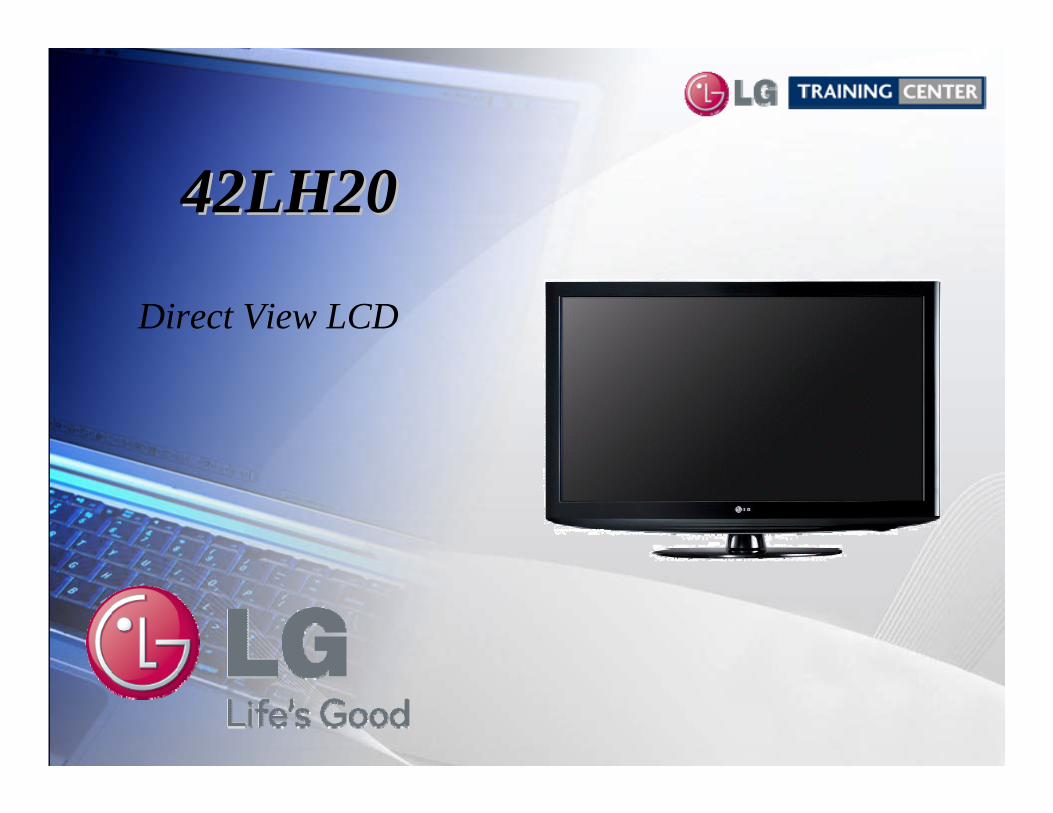
42LH2042LH20
Direct View LCD

LCD DV 42LH202 Spring 2009
OUTLINEOUTLINE
• Main Board• T-CON Board
Circuit Board Operation, Troubleshooting of :• Switch mode Power Supply
Section 1
Section 2
Contact Information, Preliminary Matters, Specifications,LCD Overview, General Troubleshooting Steps, Signal Distribution, Disassembly Instructions and Voltages
• Ft Control Board
• Side Keys
LCD DV 42LH203 Spring 2009
42LH20 LCD Direct View Display
Section 1
This Section will cover Contact Information and remind the Technician of Important Safety Precautions for the Customers Safety as well as the Technician and the Equipment.
Basic Troubleshooting Techniques which can save time and money sometimes can be overlooked. These techniques will also be presented.
This Section will get the Technician familiar with the Disassembly, Identification and Layout of the LCD Display Panel.
At the end of this Section the Technician should be able to Identify the Circuit Boards and have the ability and knowledge necessary to safely remove and replace any Circuit Board or Assembly.
Overview of Topics to be DiscussedOverview of Topics to be Discussed

LCD DV 42LH204 Spring 2009
IMPORTANT SAFETY NOTICEIMPORTANT SAFETY NOTICE
The information in this training manual is intended for use by persons possessing an adequate background in electrical equipment, electronic devices, and mechanical systems. In any attempt to repair a major Product, personal injury and property damage can result. The manufacturer or seller maintains no liability for the interpretation of this information, nor can it assume any liability in conjunction with its use. When servicing this product, under no circumstances should the original design be modified or altered without permission from LG Electronics. Unauthorized modifications will not only void the warranty, but may lead to property damage or user injury. If wires, screws, clips, straps, nuts, or washers used to complete a ground path are removed for service, they must be returned to their original positions and properly fastened.
CAUTIONCAUTION
To avoid personal injury, disconnect the power before servicing this product. If electrical power is required for diagnosis or test purposes, disconnect the power immediately after performing the necessary checks. Also be aware that many household products present a weight hazard. At least two people should be involved in the installation or servicing of such devices. Failure to consider the weight of an product could result in physical injury.
Preliminary Matters (The Fine Print)Preliminary Matters (The Fine Print)

LCD DV 42LH205 Spring 2009
Today’s sophisticated electronics are electrostatic discharge (ESD) sensitive. ESD can weaken or damage the electronics in a manner that renders them inoperative or reduces the time until their next failure. Connect an ESD wrist strap to a ground connection point or unpainted metal in the product. Alternatively, you can touch your finger repeatedly to a ground connection point or unpainted metal in the product. Before removing a replacement part from its package, touch the anti-static bag to a ground connection point or unpainted metal in the product. Handle the electronic control assembly by its edges only. When repackaging a failed electronic control assembly in an anti-static bag, observe these same precautions.
REGULATORY INFORMATIONREGULATORY INFORMATION
This equipment has been tested and found to comply with the limits for a Class B digital device, pursuant to Part 15 of the FCC Rules. These limits are designed to provide reasonable protection against harmful interference when the equipment is operated in a residential installation. This equipment generates, uses, and can radiate radio frequency energy, and, if not installed and used in accordance with the instruction manual, may cause harmful interference to radio communications. However, there is no guarantee that interference will not occur in a particular installation. If this equipment does cause harmful interference to radio or television reception, which can be determined by turning the equipment off and on, the user is encouraged to try to correct the interference by one or more of the following measures: Reorient or relocate the receiving antenna; Increase the separation between the equipment and the receiver; Connect the equipment to an outlet on a different circuit than that to which the receiver is connected; or consult the dealer or an experienced radio/TV technician for help.
ESDESD NOTICENOTICE (Electrostatic Static Discharge)(Electrostatic Static Discharge)
LCD DV 42LH206 Spring 2009
CONTACT INFORMATIONCONTACT INFORMATIONCustomer Service (and Part Sales) (800) 243-0000
Technical Support (and Part Sales) (800) 847-7597
USA Website (GCSC) aic.lgservice.com
Customer Service Website us.lgservice.com
LG CS Academy lgcsacademy.com
LG Web Training lge.webex.com
LG Electronics Alabama, Inc. 201 James Record Road, Huntsville,
AL, 35813.
http://136.166.4.200http://136.166.44.7
Published March 2009 by LG Technical Support and Training
32LG40, 42LG60, 42LG70, 47LG90, 42LH2042PG20, 50PG20, 42PQ20, 42PQ30
LCD-DV:PLASMA:
Plasma PanelAlignment Handbook

LCD DV 42LH207 Spring 2009
Safety and Handling Regulations
1. Approximately 20 minute pre-run time is required before any adjustments are performed. 2. Refer to the Voltage Sticker on the Switch Mode Power Supply silk screening. (+/- ½ volt). 3. Be cautious of electric shock from the Backlight section, it uses high voltage AC. Check that
the Power Supply and Drive Circuits are completely discharged because of residual current stored before Circuit Board removal.
4. C-MOS circuits are sensitive to static electricity. Use caution when dealing with these IC and circuits.
5. Exercise care when making voltage and waveform checks to prevent costly short circuits from damaging the unit.
6. Be cautious of lost screws and other metal objects to prevent a possible short in the circuitry.
1. Check the appearance of the Replacement Panel and Circuit Boards for both physical damage and part number accuracy.
2. Check the model label. Verify model names and board model matches.3. Check details of defective condition and history. Example: Oscillator failure dead set, etc…
Checking Points to be Considered
SECTION 1: LCD OVERVIEWSECTION 1: LCD OVERVIEW

LCD DV 42LH208 Spring 2009
Basic Troubleshooting StepsBasic Troubleshooting Steps
Define, Localize, Isolate and Correct
•Define Look at the symptom carefully and determine what circuits could be causing the failure. Use your senses Sight, Smell, Touch and Hearing. Look for burned parts and check for possible overheated components. Capacitors will sometimes leak dielectric material and give off a distinct odor. Frequency of power supplies will change with the load, or listen for relay closing etc. Observation of the front Power LED may give some clues.
•Localize After carefully checking the symptom and determining the circuits to be checked and after giving a thorough examination using your senses the first check should always be the DC Supply Voltages to those circuits under test. Always confirm the supplies are not only the proper level but be sure they are noise free. If the supplies are missing check the resistance for possible short circuits.
•Isolate To further isolate the failure, check for the proper waveforms with the Oscilloscope to make a final determination of the failure. Look for correct Amplitude Phasing and Timing of the signals also check for the proper Duty Cycle of the signals. Sometimes “glitches” or “road bumps” will be an indication of an imminent failure.
•Correct The final step is to correct the problem. Be careful of ESD and make sure to check the DC Supplies for proper levels. Make all necessary adjustments and lastly always perform a Safety AC Leakage Test before returning the product back to the Customer.

LCD DV 42LH209 Spring 2009
This section of the manual will discuss the specifications of the 42LH20LCD Direct View Display Panel.
42LH20 Product Information42LH20 Product Information

LCD DV 42LH2010 Spring 2009
Basic SpecificationsBasic Specifications
Key Features• 42" Screen • 720p HD Resolution • Two (2) HDMI(TM) (V.1.3 with Deep Color) • ISFccc Ready • Smart Energy Saving • LG SimpLink (TM) (32-inch and above) • LG Core Technologies (32-inch and above) • Dynamic Contrast Ratio 12,000:1 • Response Time (G to G) 8ms • Brightness 500 cd/m2 • Viewing Angle 178º / 178º• Life Span (Typical) 60,000 hr • Built-in Tuner ATSC/NTSC/Clear QAM • HDMI™/HDCP Input 2 v1.3 • Cabinet Color Glossy Piano-Black • Limited Warranty 1 Year Parts/Labor

LCD DV 42LH2011 Spring 2009
SDEDHDHDHD
Interlaced2 Fields to make a Frame
ProgressiveEach Field is a Frame
Think of sync as the Panels “Refresh Rate”
Possible FrameRates:24FPS30FPS60FPS
PANEL PIXELS (Logo Familiarization Explained)PANEL PIXELS (Logo Familiarization Explained)
BASICPIXEL COUNTS
720P PANEL1365 (H) × 768 (V)
1080P PANEL1920 (H) x 1080 (V)
HD RESOLUTION 720p HD Resolution Pixels: 1366 (H) × 768 (V)High definition television is the highest performance segment of the DTV system used in the US. It’s a wide screen, high-resolution video image, coupled with multi-channel, compact-disc quality sound.
FORMATS480I480P1080I720P1080P
InterlacedProgressiveInterlacedProgressiveProgressive
240 Lines480 Lines540 Lines720 Lines1080 Lines
Lines Per Field
LCD DV 42LH2012 Spring 2009
Basic Specifications (LOGO Familiarization) Page 1Basic Specifications (LOGO Familiarization) Page 1
SIMPLINKAllows for convenient control of other LG SimpLink products using the existing HDMI connection.
Clear Voice Technology Automatically enhances and amplifies the sound of the human voice frequency range to provide high-quality dialogue when background noise swells.
LCD DV 42LH2013 Spring 2009
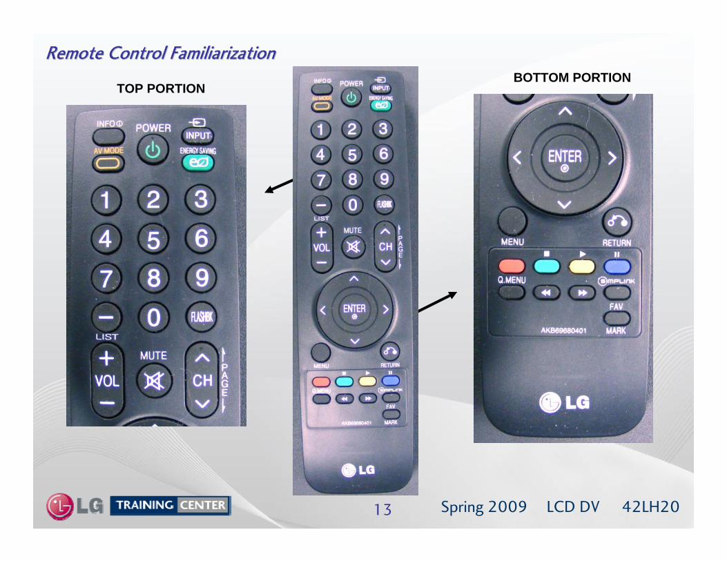
TOP PORTIONBOTTOM PORTION
Remote Control FamiliarizationRemote Control Familiarization

LCD DV 42LH2014 Spring 2009
Accessing the Service MenuAccessing the Service Menu
REMOTETOP PORTION
SIDE KEYS
To access the Service Menu.1) Turn the Set On2) Simultaneously, Press and
“Hold” the Menu Key on the Side Key pad and Press and “Hold” the Menu Key on the Remote approximately 5 seconds.
3) If Customer’s Menu appears, continue to hold until it disappears.
4) The Service Menu appears
Note: If a Password is required to enter the Service Menu. Enter;
0000

LCD DV 42LH2015 Spring 2009
Rear and Side Input JacksRear and Side Input Jacks
Main PWBOrientation
Rear Input Jacks
USB PortFor Software
Upgrades Only
LCD DV 42LH2016 Spring 2009
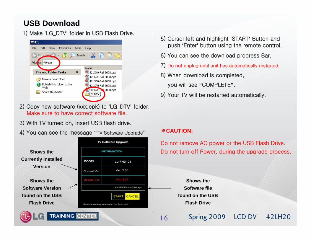
USB Download1) Make 'LG_DTV' folder in USB Flash Drive.
5) Cursor left and highlight ‘START’ Button and push ‘Enter’ button using the remote control.
6) You can see the download progress Bar.
7) Do not unplug until unit has automatically restarted.
8) When download is completed,
you will see “COMPLETE”.
9) Your TV will be restarted automatically.
※CAUTION:
Do not remove AC power or the USB Flash Drive.
Do not turn off Power, during the upgrade process.
2) Copy new software (xxx.epk) to 'LG_DTV' folder.Make sure to have correct software file.
3) With TV turned on, insert USB flash drive.
4) You can see the message “TV Software Upgrade”
Shows theCurrently Installed
Version
Shows theSoftware Versionfound on the USB
Flash Drive
Shows theSoftware file
found on the USBFlash Drive
LCD DV 42LH2017 Spring 2009
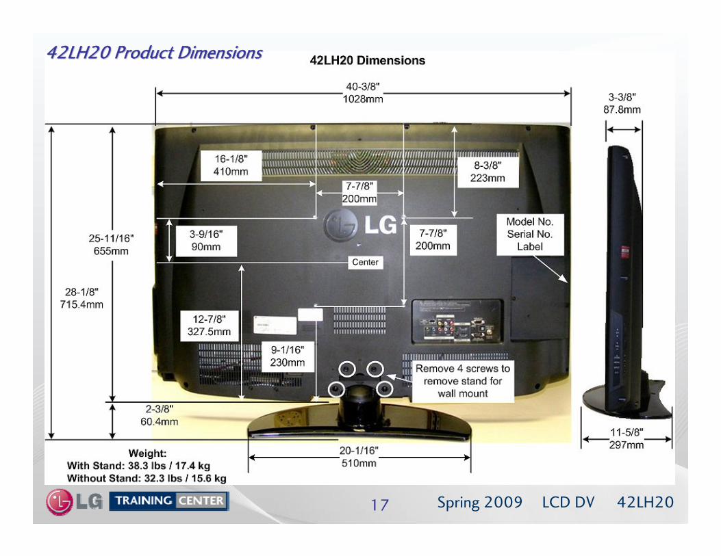
42LH20 Product Dimensions42LH20 Product Dimensions
LCD DV 42LH2018 Spring 2009
Disassembly:This section of the manual will discuss Disassembly, Layout and Circuit Board Identification, of the 42LH20 LCD Direct View Television.
Upon completion of this section the Technician will have a better understanding of the disassembly procedures, the layout of the printed circuit boards and be able to identify each board.
Troubleshooting:This section of the manual will also discuss troubleshooting.
Upon completion of this section the Technician will have a better understanding of how to diagnosis and resolve problems.
DISASSEMBLY AND TROUBLESHOOTING SECTIONDISASSEMBLY AND TROUBLESHOOTING SECTION

LCD DV 42LH2019 Spring 2009
Removing the Back Step (1)Removing the Back Step (1)
Remove the Stand byPulling it out of itsRetaining bracket.
Lay the TV down on its face. Remove the 4 screws around stand indicated by the arrows.
Remove the one screw hidden by the stand.
Reinsert the stand and
stand the unit upright for
service position to continue
removing the back cover.
Remove

LCD DV 42LH2020 Spring 2009
The Stand has to be removed first.Remove the 22 screws indicated.
Pay attention to the size and type of screwas there are many different types.
Putting in the improper screw when reassembling may Cause damage.
Remove the one screw hidden under the stand.
See previous page.
Removing the Back Cover Step 2 (Stand has to be removed)Removing the Back Cover Step 2 (Stand has to be removed)
LCD DV 42LH2021 Spring 2009
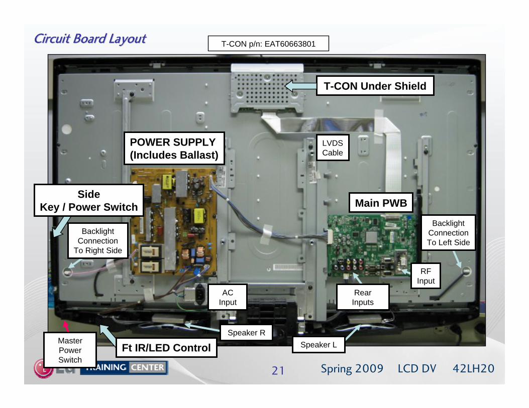
Circuit Board LayoutCircuit Board Layout
POWER SUPPLY(Includes Ballast)
Main PWB
LVDSCable
BacklightConnection
To Right Side
T-CON Under Shield
Ft IR/LED Control
AC Input
RFInput
Speaker R
Rear Inputs
BacklightConnectionTo Left Side
MasterPower Switch
SideKey / Power Switch
Speaker L
T-CON p/n: EAT60663801

LCD DV 42LH2022 Spring 2009
Power Supply PWB RemovalPower Supply PWB Removal
Disconnect P201, AC In and SK102, P401 and P402.
Remove the 6 screws indicated by the arrows.
P201
AC In
SK102
P402
P401
LCD DV 42LH2023 Spring 2009
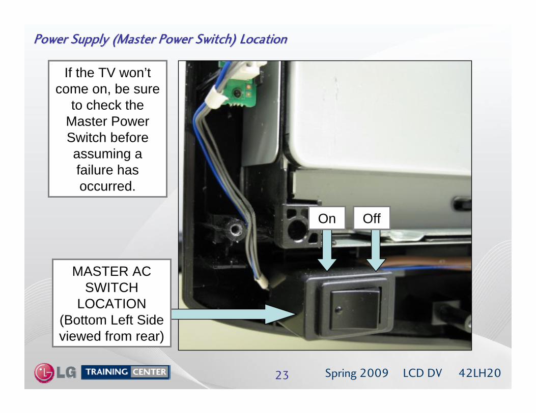
Power Supply (Master Power Switch) LocationPower Supply (Master Power Switch) Location
MASTER AC SWITCH
LOCATION(Bottom Left Side viewed from rear)
On Off
If the TV won’t come on, be sure
to check the Master Power Switch before assuming a failure has occurred.

LCD DV 42LH2024 Spring 2009
Power Supply (SMPS) PWB LayoutPower Supply (SMPS) PWB Layout Hot Ground Shock Hazard
To MainP201
AC INSK101
F1006.3A/250V
AC IN
F5013.15A/250VRun 380V
STBY 168VFrom Hot Gnd
ToMaster Power Switch
SK102
L
N
Pin 1 Pin 2
To BacklightsLeft SideP402
To BacklightsRight Side
P401
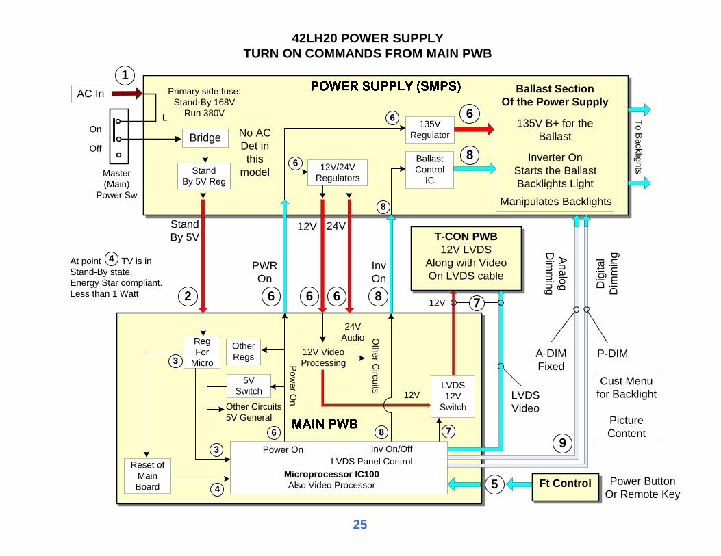
T-CON PWB12V LVDS
Along with VideoOn LVDS cable
Inverter OnStarts the BallastBacklights Light
135V B+ for the Ballast
Stand By 5V
Power ButtonOr Remote Key
Reset ofMain Board
5V Switch
PWROn
12V VideoProcessing
InvOn
BallastControl
IC
135VRegulator
12V/24V Regulators
Other Regs
StandBy 5V Reg
1
2 6 66 8
8
6
3
5
42LH20 POWER SUPPLYTURN ON COMMANDS FROM MAIN PWB
6
6
6
Primary side fuse:Stand-By 168V
Run 380V
4
24V Audio
12V 24V
8
RegFor
Micro
LVDS12V
Switch12V
7
7
At point TV is in Stand-By state. Energy Star compliant.Less than 1 Watt
4
Other Circuits 5V General
A-DIMFixed
P-DIM
Manipulates Backlights
Other C
ircuits
9
Cust Menu for Backlight
Picture Content
Power O
n
3
8
Ballast SectionOf the Power Supply
No AC Det in this
model
To Backlights
LVDS Panel ControlInv On/Off
Microprocessor IC100Also Video Processor
LVDSVideo
12V
Power On
AC In
25
Ft Control
Analog
Dim
ming D
igita
lD
imm
ing
Bridge
Master(Main)
Power Sw
On
Off
L

PWM-DIM (PWM Dimming) Manipulates the Backlight Brightness via Customer’s OSD.Manipulates the Backlight Brightness via the BCM Chip. Darker Picture, Darker Backlights to facilitate improved Contrast Ratio. 0.6V ~ 3.3V Range
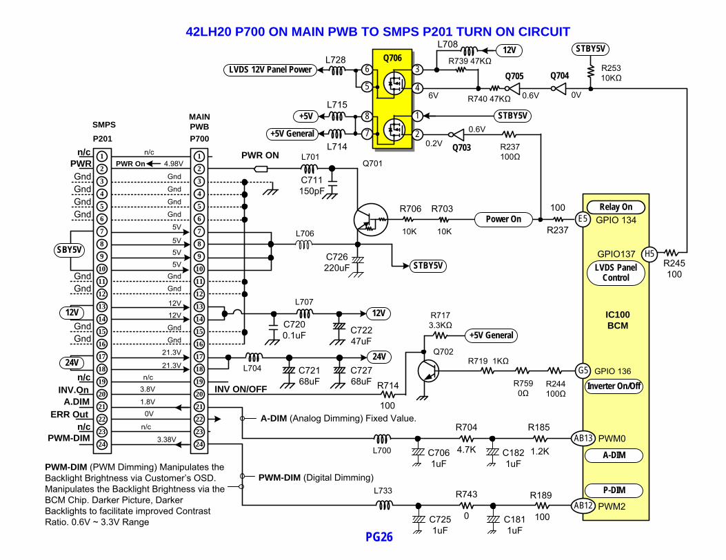
42LH20 P700 ON MAIN PWB TO SMPS P201 TURN ON CIRCUIT
R189
R185
1.2K
INV ON/OFF
PWR ON
100
R714
R704
C711150pF
C1811uF
P700
12V12V
Gnd
Gnd
Gnd
Gnd
0V
3.38V
4.98V
1.8V
PWR On
P201
ERR Out
PWR
A.DIMINV.On
PWM-DIM
n/c
SMPS
AB12
IC100BCM
PWM2
PWM0
100
n/c
GndGndGndGnd
A-DIM (Analog Dimming) Fixed Value.
100
H5R245100
GPIO137SBY5V
MAINPWB
5V
5V5V5V
GndGnd
12V
2
1
4
3
6
5
8
7
10
9
11
12
14
13
16
15
18
17
20
19
22
21
23
24
2
1
4
3
6
5
8
7
10
9
11
12
14
13
16
15
18
17
20
19
22
21
23
24
21.3V24V
GndGnd
GndGndGndGnd
n/c n/c
n/c n/c
E5 GPIO 134L706
L70424V
C72168uF
C72768uF
L70712V
C7200.1uF C722
47uF
L701Q701
R703R706
R237
G5R719 1KΩ
Q702
R759 0Ω
R717 3.3KΩ
GPIO 136R244 100Ω
+5V General
Power On
Inverter On/Off
3
1
2
6
5
8
7
Q706
+5VL715
+5V GeneralL714
LVDS 12V Panel PowerL728
Q703 R237 100Ω
0.2V
6V
0.6V
4Q704Q705
LVDS Panel Control
L708
R25310KΩ
0V0.6V
12VR739 47KΩ
R740 47KΩ
AB13
PWM-DIM (Digital Dimming)
C726220uF STBY5V
L700
R743
0
L733
Relay On
A-DIM
P-DIM
STBY5V
STBY5V
4.7K C1821uF
C7251uF
C7061uF
21.3V
3.8V
10K10K
PG26

LCD DV 42LH2027 Spring 2009
Power Supply (SMPS) PWB Operational TroubleshootingPower Supply (SMPS) PWB Operational Troubleshooting
Power Supply Troubleshooting
Ac voltage is supplied to the Power Supply at Connector SC100. This set does not use AC Detect. The AC input generates a Hot Ground primary power supply that runs in two states, Stand-By (168) and Run (380V) measured at Fuse F501. This primary voltage develops all other voltages that are output from the power supply. During Stand-By, the 5 Volt Standby should be present at connector P201, Pins7,8,9 or 10. If Missing remove AC Power and unplug Connector P201, apply AC Power and recheck for presence of 5 Volt Standby. Loss of 5 Volt Standby would be a Power Supply Failure. Presence of 5 Volt Standby would be an indication of a failure on the Main Board or possibly the Front PWB (IR) assembly. Suspect a possible short circuit loading the supply. Remember to observe the Front Power Indicating LED this may save some time. A lit LED indicates the Stand-By 5V voltage is present!
The Main Board sends two commands to the Power Supply Board one being PWR the other is INV ON. These two voltages are used to control the power on turn on sequence. First via PWR (Pin 2) also known as POWER ON, activates the internal Ballast voltage and the 24 Volt and 12 Volt lines to the Main board. The 2nd command is INV ON (P201 pin 20). It it the Lamp Lighting Command Signal. If either command (PWR-ON or INV-ON) is missing it will result in a no picture symptom.
These voltages can easily be checked with the volt meter! Remove AC Power, unplug the two Connectors to the backlights P401/P402. Reapply AC Power and press the ON-OFF Button on either the Remote Control or Power Button on the Unit. Watch for the Power ON LED to change color from red to blue. This is an indication the PWR Signal was created on the the Main board. Check P700 or P201 pin 2 for the PWR-ON command (2.8V) to the Power Supply. Check P201 for 24V (Pins 17 or 18) and 12V (Pins 13 or 14). Confirm Pin 20 of P201 went to 3.3V. This is the INV ON signal needed to light the Lamps.Problems with either voltage can be easily solved by following the simple steps on the next page.

LCD DV 42LH2028 Spring 2009
TEST 1 Power Supply PWB Low Voltage TestTEST 1 Power Supply PWB Low Voltage Test
AC Should not be applied at any time while adding resistors or while unplugging connectors as damage to the circuit PWB may occur.
a) The SMPS PWB “MUST” be producing STBY 5V on any of thepins 7, 8, 9 or 10 (5V).
If 5V Standby is not being generated, the SMPS PWB is defective and must be replaced. There is no need to continue with the next test.
(b) Unplug P700 on the Main PWB.
TEST 1:
(1) Add a 10K resistor between (5V STBY) pin 7, 8, 9 or 10 and Pin 2 (PWR). Apply AC. This will turn on the power supply.
• Check that the 24V and 12V power supplies areturned on, P201 (24V pins 17 and 18) (12V pins 13 and 14)
(2) Remove AC power.
Use P700Side to insert
resistors
LCD DV 42LH2029 Spring 2009
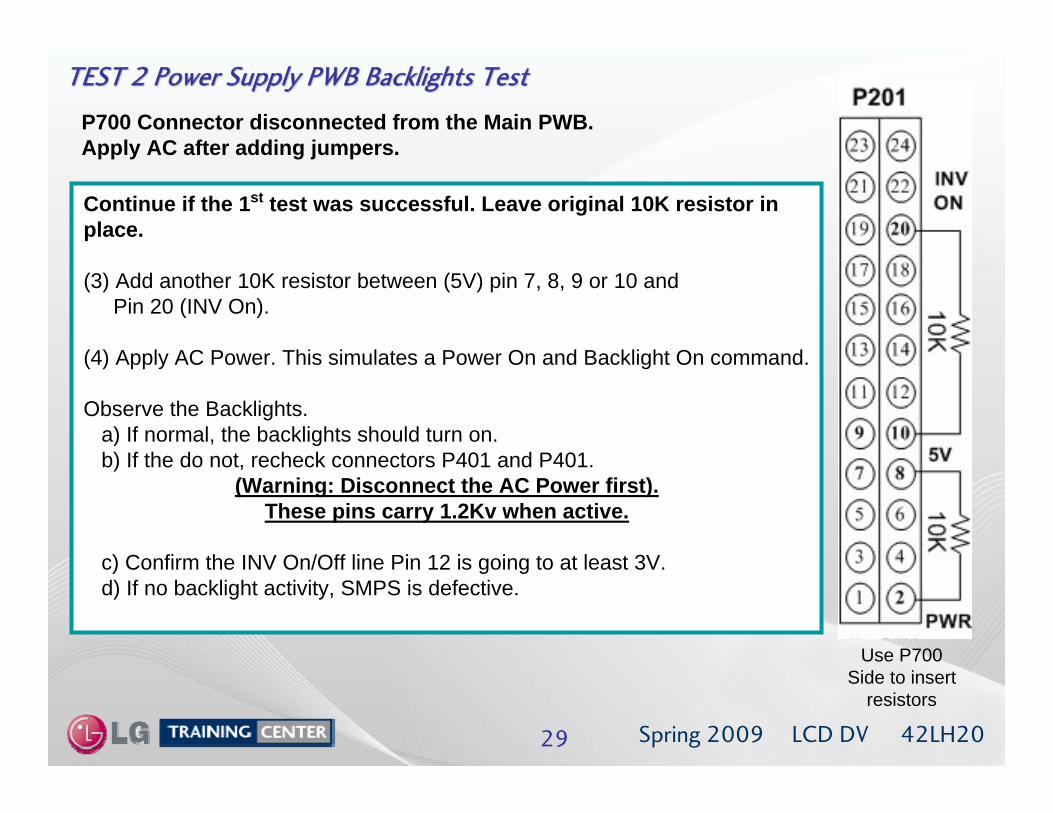
Continue if the 1st test was successful. Leave original 10K resistor in place.
(3) Add another 10K resistor between (5V) pin 7, 8, 9 or 10 and Pin 20 (INV On).
(4) Apply AC Power. This simulates a Power On and Backlight On command.
Observe the Backlights.a) If normal, the backlights should turn on.b) If the do not, recheck connectors P401 and P401.
(Warning: Disconnect the AC Power first). These pins carry 1.2Kv when active.
c) Confirm the INV On/Off line Pin 12 is going to at least 3V.d) If no backlight activity, SMPS is defective.
TEST 2 Power Supply PWB Backlights TestTEST 2 Power Supply PWB Backlights Test
P700 Connector disconnected from the Main PWB.Apply AC after adding jumpers.
Use P700Side to insert
resistors
LCD DV 42LH2030 Spring 2009
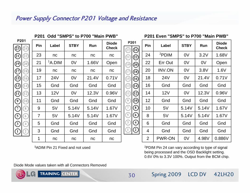
Power Supply Connector P201 Voltage and ResistancePower Supply Connector P201 Voltage and Resistance
Diode Mode values taken with all Connectors Removed
0.886V4.98V0VPWR-ON2
GndGndGndGnd4
GndGndGndGnd6
1.67V5.14V5.14V5V8
1.67V5.14V5.14V5V10
GndGndGndGnd12
0.96V12.3V0V12V14
GndGndGndGnd16
0.71V21.4V0V24V18
1.6V3.8V0VINV.ON20
Open0V0VErr Out22
1.68V3.2V0V2PDIM24
Diode CheckRun STBYLabelPin
P201 Even "SMPS" to P700 "Main PWB"
ncncncnc1
GndGndGndGnd3
GndGndGndGnd5
1.67V5.14V5.14V5V7
1.67V5.14V5.14V5V9
GndGndGndGnd11
0.96V12.3V0V12V13
GndGndGndGnd15
0.71V21.4V0V24V17
ncncncnc19
Open1.66V0V1A.DIM21
ncncncnc23
Diode CheckRun STBYLabelPin
P201 Odd "SMPS" to P700 "Main PWB"
1ADIM Pin 21 Fixed and not used 2PDIM Pin 24 can vary according to type of signal being processed and the OSD Backlight setting. 0.6V 0% to 3.3V 100%. Output from the BCM chip.
LCD DV 42LH2031 Spring 2009
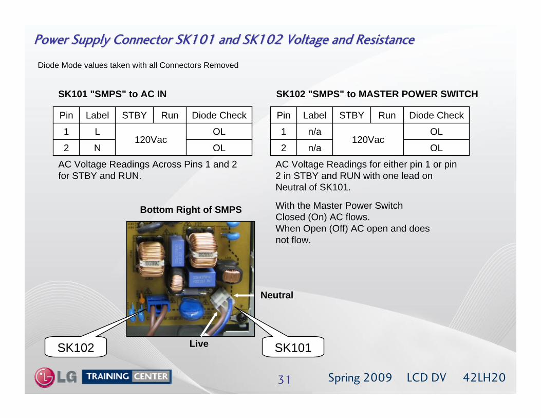
Power Supply Connector SK101 and SK102 Voltage and ResistancePower Supply Connector SK101 and SK102 Voltage and Resistance
Diode Mode values taken with all Connectors Removed
AC Voltage Readings Across Pins 1 and 2 for STBY and RUN.
OLN2
OL120Vac
L1
Diode CheckRun STBYLabelPin
AC Voltage Readings for either pin 1 or pin 2 in STBY and RUN with one lead on Neutral of SK101.
OLn/a2
OL120Vac
n/a1
Diode CheckRun STBYLabelPin
SK101 "SMPS" to AC IN SK102 "SMPS" to MASTER POWER SWITCH
SK102 SK101
Bottom Right of SMPS
Live
Neutral
With the Master Power SwitchClosed (On) AC flows.When Open (Off) AC open and does not flow.

LCD DV 42LH2032 Spring 2009
General Backlight InformationGeneral Backlight Information
To Backlights Over 1.2KV
Currently, number of lamps “Unknown”
To Backlights Over 1.2KV
Ballast Section of SMPS
EEFL (External Electrode Fluorescent Lamp)LOW COST Large number of lamps driven by a single inverter
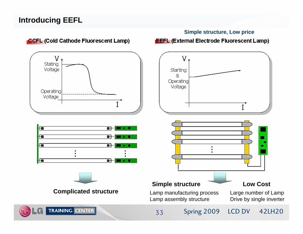
LCD DV 42LH2033 Spring 2009
Simple structure, Low price
Complicated structureSimple structure
Lamp manufacturing processLamp assembly structure
Low CostLarge number of Lamp Drive by single inverter
Introducing EEFL

LCD DV 42LH2034 Spring 2009
Introducing EEFL Contacts (Bulb Design)
Key: Long Life Time
• For CCFL, Hg gas is consumed mainly near the internal electrode• For EEFL, longer life time is expected because there is no internal electrode consuming Hg gas
LCD DV 42LH2035 Spring 2009
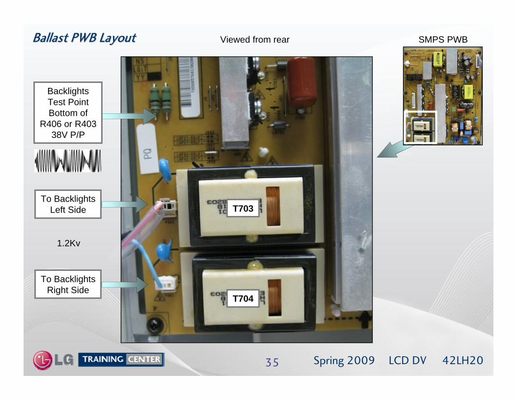
Ballast PWB LayoutBallast PWB Layout
To BacklightsLeft Side T703
T704
Viewed from rear
To BacklightsRight Side
SMPS PWB
BacklightsTest PointBottom of
R406 or R40338V P/P
1.2Kv
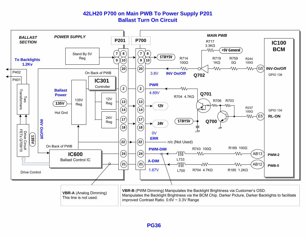
42LH20 P700 on Main PWB To Power Supply P201Ballast Turn On Circuit
PG36
IC100BCM
R743 100Ω
R7191KΩ
R704 4.7KΩ
A-DIM
PWM-DIM
INV On/Off3.8V
VBR-B (PWM Dimming) Manipulates the Backlight Brightness via Customer’s OSD.Manipulates the Backlight Brightness via the BCM Chip. Darker Picture, Darker Backlights to facilitate improved Contrast Ratio. 0.6V ~ 3.3V Range
INV-On/Off
PWB-0AB12
AB13 PWM-2
20
24
21
R189 100Ω
R185 1.2KΩ
R244100Ω
G5
VBR-A (Analog Dimming)This line is not used.
P700POWER SUPPLY
RL-ON
PWR
4.89V2
12VReg
24VReg
13
14
17
18
135V
BALLAST SECTION
1.67V
IC301
135VReg
ERR0V
n/c (Not Used)22
P201MAIN PWB
20
24
21
2
13
14
17
18
22
IC600Ballast Control IC
12V
24V
On Back of PWB
On Back of PWB
INV O
n/Off
To Backlights1.2Kv
Two
Transformers
Drive C
ircuitFE
Ts Q709/10
Drive Control
Q702
R704 4.7KΩ
R7590Ω
R714100Ω
GPIO 134
GPIO 136
R237100Ω
Q701
Q700
R703R706
E5
7 8
9 10
7 8
9 10STBY5V
STBY5V
L700
L733
BallastPower
Hot Gnd
135V
P401
P402
Stand By 5VReg
Controller
R717 3.3KΩ
+5V General
LCD DV 42LH2037 Spring 2009
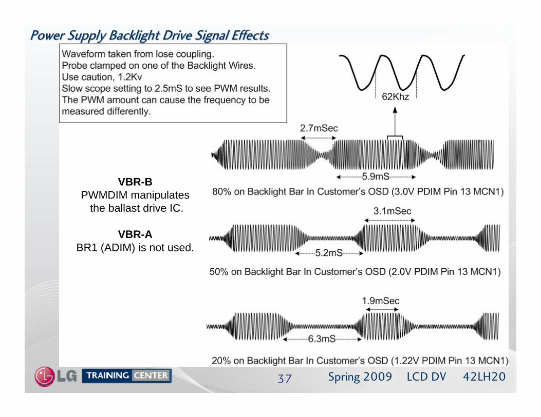
Power Supply Backlight Drive Signal EffectsPower Supply Backlight Drive Signal Effects
VBR-BPWMDIM manipulates
the ballast drive IC.
VBR-ABR1 (ADIM) is not used.

LCD DV 42LH2038 Spring 2009
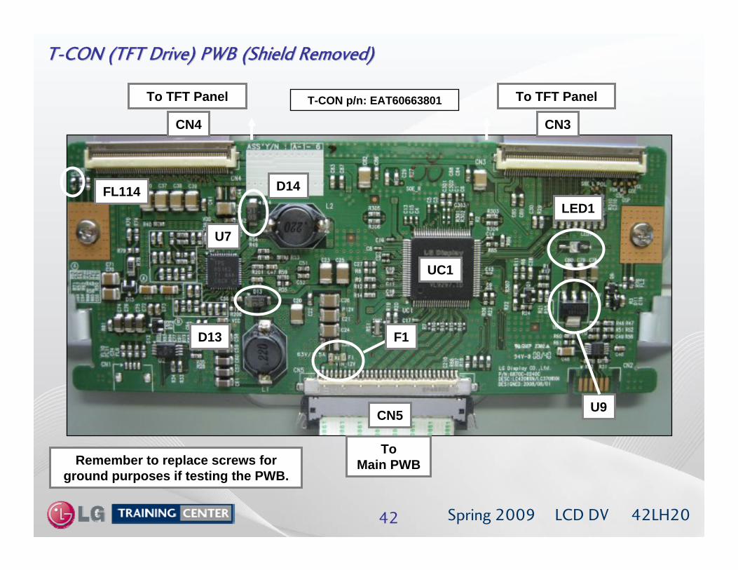
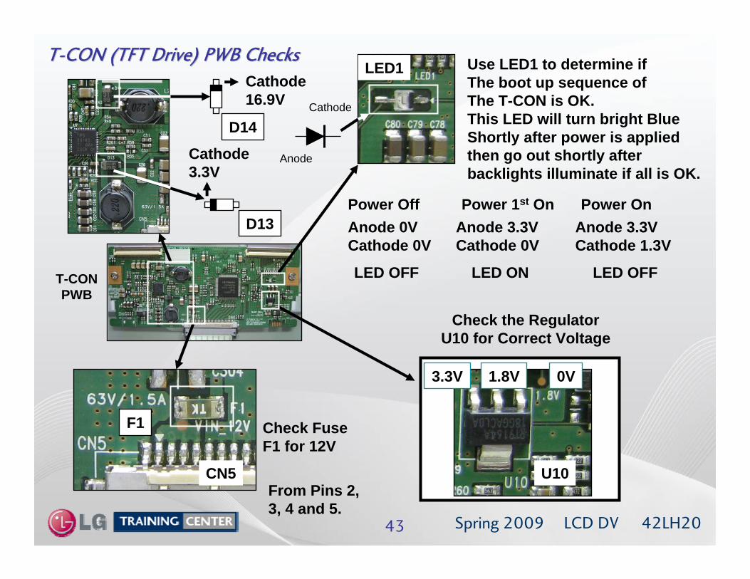
TT--CON (TFT DRIVE) PWB CON (TFT DRIVE) PWB
LCD Controller BoardThe T-Con IC UC1 receives from the Main Board at CN5 12 Bit
LVDS Signals (Video) which it processes into TFT Drive Signals which through connectors CN3 and CN4 controls the LCD Panel.
12V is supplied to the T-Con Board on connector CN5 from the Main Board(easily measured at fuse F1).
Diode LED1 is a boot up indicator and is helpful in troubleshooting as a quick indication of a loss of supply and or a Boot Up problem.
There are two DC to DC converters that create (17V developed at the cathode of D14) and (3.3V developed at the cathode of D13).
The 3.3V can also be measured at the ribbon connectors delivering signals to the TFT panel (CN3 pins 57, 58 or 59) and (CN4 pins 2, 3 or 4).

LCD DV 42LH2039 Spring 2009
TT--CON (TFT Drive) PWB RemovalCON (TFT Drive) PWB Removal
Remove the 3 Screws in the T-CON shield and remove the shield
CN4 CN3
CN5
Disconnect CN3, CN4 and CN5.See next slide for details.
The two screws shown in the picture below arefor the Service Position.
They would have been removedwhen removing the shield. Be sure to reinstall them ifservicing the T-CON PWB.

LCD DV 42LH2040 Spring 2009
TT--CON (TFT DRIVE) PWB REMOVAL CONTINUED:CON (TFT DRIVE) PWB REMOVAL CONTINUED:
To remove the flex cables to the TFT Panel, CN3 or CN4: Place a soft thin object like a fingernail underneath the black locking tab and gently pull forward.
(Shown by the arrows in Fig 1)
Fig 1
Fig 2
Unlocked
Flip the lock up and back from the flex cable. Then the flex cable can be easily removed. To remove the LVDS cable CN5;
Press in on the two tabs and slowly rock the cable out of the connector.
(Shown by the arrows in Fig 3)
Fig 3 (CN5) LVDS
UNLOCKING CN3, CN4 and CN5UNLOCKING CN3, CN4 and CN5
The locking tab is flipped upward
Press In Press In
Pull Out
CN3 or CN4 Locked
LCD DV 42LH2041 Spring 2009
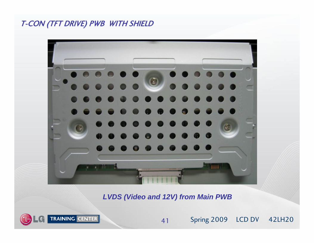
TT--CON (TFT DRIVE) PWB WITH SHIELDCON (TFT DRIVE) PWB WITH SHIELD
LVDS (Video and 12V) from Main PWB
LCD DV 42LH2042 Spring 2009
TT--CON (TFT Drive) PWB (Shield Removed)CON (TFT Drive) PWB (Shield Removed)
U7
D13
U9
LED1
F1
CN4 CN3
CN5
UC1
ToMain PWB
To TFT Panel To TFT Panel
Remember to replace screws for ground purposes if testing the PWB.
D14FL114
T-CON p/n: EAT60663801
LCD DV 42LH2043 Spring 2009
TT--CON (TFT Drive) PWB ChecksCON (TFT Drive) PWB Checks
T-CON PWB
LED1 Use LED1 to determine ifThe boot up sequence ofThe T-CON is OK.This LED will turn bright BlueShortly after power is applied then go out shortly after backlights illuminate if all is OK.
Power Off Power 1st OnAnode 0VCathode 0V
Anode 3.3VCathode 0V
Power OnAnode 3.3VCathode 1.3V
LED OFF LED ON LED OFF
1.8V3.3V 0V
U10
Check the Regulator U10 for Correct Voltage
Check FuseF1 for 12V
F1
CN5
Cathode 16.9V
Cathode 3.3V
D14
D13
Anode
Cathode
From Pins 2, 3, 4 and 5.

LCD DV 42LH2044 Spring 2009
CN4
TT--CON (TFT Driver) Board CN3 and CN4 (3.3V Voltage Check)CON (TFT Driver) Board CN3 and CN4 (3.3V Voltage Check)
3.3V Check3.3V Check
If the 3.3Volts is missing, check the 3.3V DC to DC converter. Check at D13 cathode. See previous page for location.
CN3
T-CON PWB
LCD DV 42LH2045 Spring 2009
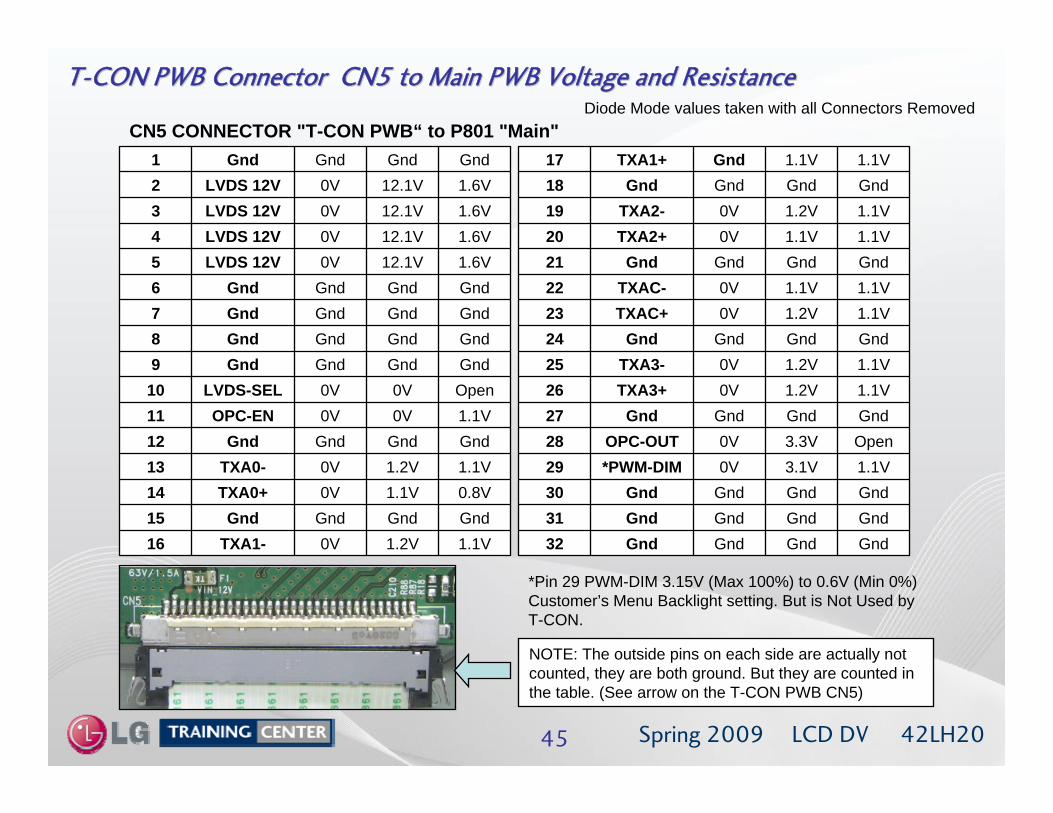
TT--CON PWB Connector CN5 to Main PWB Voltage and ResistanceCON PWB Connector CN5 to Main PWB Voltage and ResistanceDiode Mode values taken with all Connectors Removed
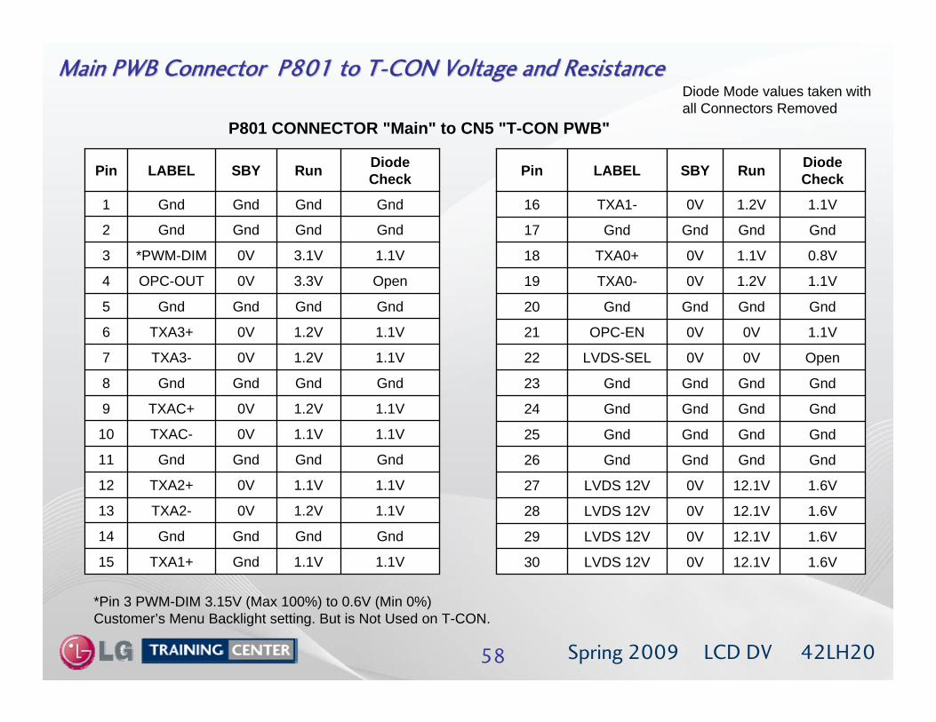
CN5 CONNECTOR "T-CON PWB“ to P801 "Main"
*Pin 29 PWM-DIM 3.15V (Max 100%) to 0.6V (Min 0%) Customer’s Menu Backlight setting. But is Not Used by T-CON.
1.1V1.2V0VTXA1-16GndGndGndGnd150.8V1.1V0VTXA0+141.1V1.2V0VTXA0-13GndGndGndGnd121.1V0V0VOPC-EN11Open0V0VLVDS-SEL10GndGndGndGnd9GndGndGndGnd8GndGndGndGnd7GndGndGndGnd61.6V12.1V0VLVDS 12V51.6V12.1V0VLVDS 12V41.6V12.1V0VLVDS 12V31.6V12.1V0VLVDS 12V2GndGndGndGnd1
GndGndGndGnd32GndGndGndGnd31GndGndGndGnd301.1V3.1V0V*PWM-DIM29Open3.3V0VOPC-OUT28GndGndGndGnd271.1V1.2V0VTXA3+261.1V1.2V0VTXA3-25GndGndGndGnd241.1V1.2V0VTXAC+231.1V1.1V0VTXAC-22GndGndGndGnd211.1V1.1V0VTXA2+201.1V1.2V0VTXA2-19GndGndGndGnd181.1V1.1VGndTXA1+17
NOTE: The outside pins on each side are actually not counted, they are both ground. But they are counted in the table. (See arrow on the T-CON PWB CN5)

LCD DV 42LH2046 Spring 2009
Main PWB IC100 Video Processor OverviewMain PWB IC100 Video Processor Overview
Input Signal Processing IC100 is the main Microprocessor and the main Signal Processor and is responsible for :
• ATSC, NTSC, and QAM reception and processing• RS 232 service only Port (software upgrades and home theater environment).• Wired Remote Port• (1) Component Input Y, Pr, Pb and Audio L R• (2) HDMI Inputs (back) (1) HDMI (Side Input) • RGB PC and (PC Audio)• USB (software upgrades using flash drive). USB located on the Rear, no Side Inputs.• AV Composite• SIF and SAP
Output Signals
•10 Bit LVDS (10 Pin) to the T-CON Board• Audio output signals to the Speakers• Digital Audio Output Coaxial and Optical• ON OFF Controls to the SMPS turning on low voltage generation and Backlights• Backlight intensity control signal (Digital Dimming) P-DIM

LCD DV 42LH2047 Spring 2009
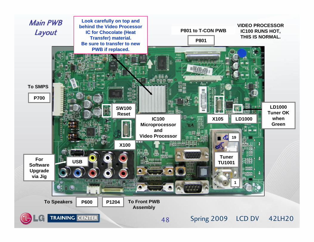
Removing the Main PWBRemoving the Main PWB
Remove the one screws at the bottom of the Decorative plastic piece on the right side. Remove the plastic piece.
Remove the two pieces of tape on the left side holding down the cables and the one at the top.
Remove the remaining 11 screws indicated by the arrows.
Decorative Plastic
P700
P801
P600P1204
Flip the locking tabs upward, pull the LVDS ribbon out.
NOTE: Be sure to check on top and behind the Video Processor IC. Look for a piece of
Chocolate(Heat Transfer Material).
Be sure to transfer to new PWB if present.
LCD DV 42LH2048 Spring 2009
Main PWB Main PWB LayoutLayout
VIDEO PROCESSOR IC100 RUNS HOT, THIS IS NORMAL.
1
19
LD1000 Tuner OK
when Green
P700
P801
P1204
IC100Microprocessor
andVideo Processor
X100
USBTuner
TU1001
To SMPS
To Front PWB Assembly
P801 to T-CON PWB
To Speakers
Look carefully on top and behind the Video Processor
IC for Chocolate (Heat Transfer) material.
Be sure to transfer to new PWB if replaced.
For Software Upgrade via Jig
SW100Reset
X105
P600
LD1000

LCD DV 42LH2049 Spring 2009
Main PWB Main PWB (Back View)(Back View) Voltages given on the 11X17 foldout “Interconnect Diagram”
IC1003
IC1002
Tuner
IC702
IC601
IC500IC501
IC501
IC102
LCD DV 42LH2050 Spring 2009
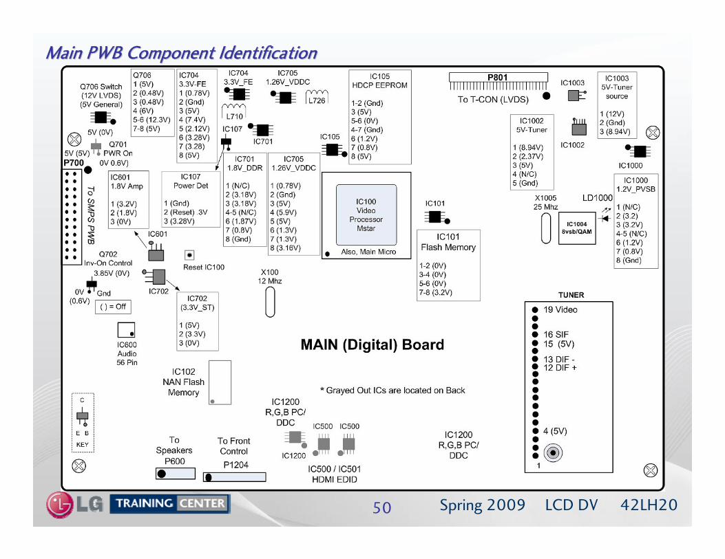
Main PWB Component IdentificationMain PWB Component Identification

LCD DV 42LH2051 Spring 2009
Main PWB X100 and X1005 CheckMain PWB X100 and X1005 Check
X1005 LocationX100
Location
2.28Vp/p12Mhz
Set on or off
X400
IC100 Microprocessor Crystal
MAIN PWB
4.95Vp/p 25Mhz
X1005
Tuner Control IC1004 Crystal
Only when set is on
X100
LCD DV 42LH2052 Spring 2009
MAIN PWB
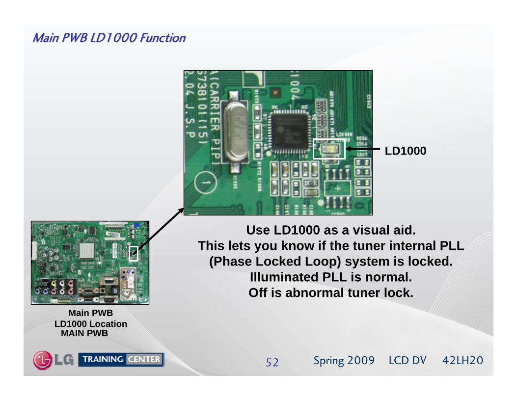
Main PWB LD1000 FunctionMain PWB LD1000 Function
Main PWBLD1000 Location
LD1000
Use LD1000 as a visual aid.This lets you know if the tuner internal PLL
(Phase Locked Loop) system is locked. Illuminated PLL is normal. Off is abnormal tuner lock.

LCD DV 42LH2053 Spring 2009
Main PWB Tuner with Shield Off (Pin ID)Main PWB Tuner with Shield Off (Pin ID)
1
19
18
4
13
12
9
8
LCD DV 42LH2054 Spring 2009
MAIN PWB
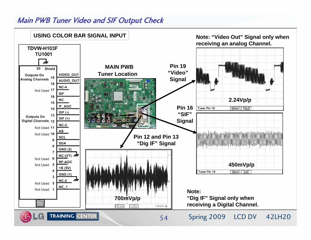
Main PWB Tuner Video and SIF Output CheckMain PWB Tuner Video and SIF Output Check
Tuner Location
450mVp/p
Pin 19 “Video”Signal
Pin 16 “SIF”Signal
2.24Vp/p
USING COLOR BAR SIGNAL INPUT
Pin 12 and Pin 13“Dig IF” Signal
Note:“Dig IF” Signal only when receiving a Digital Channel.
700mVp/p
Pin 1
Note: “Video Out” Signal only when receiving an analog Channel.

LCD DV 42LH2055 Spring 2009
Main PWB Tuner Clock and Data LinesMain PWB Tuner Clock and Data Lines
Pin 8 SDA
100uS1V per/div 5V p/p
Pin 9 SCL
100uS1V per/div 5V p/p
Note:SCL and SDA only active during an actual Channel Change.
LCD DV 42LH2056 Spring 2009
MAIN PWB
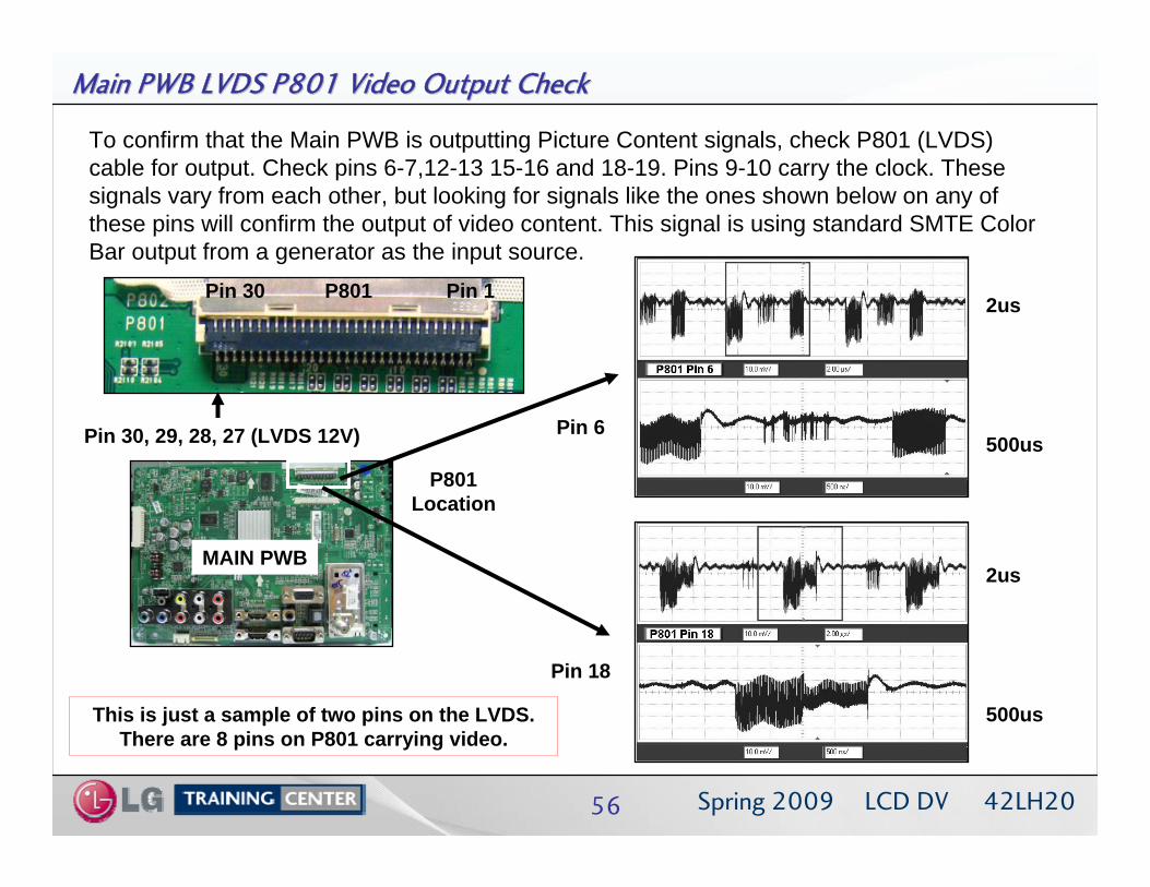
Main PWB LVDS P801 Video Output CheckMain PWB LVDS P801 Video Output Check
P801Location
To confirm that the Main PWB is outputting Picture Content signals, check P801 (LVDS) cable for output. Check pins 6-7,12-13 15-16 and 18-19. Pins 9-10 carry the clock. These signals vary from each other, but looking for signals like the ones shown below on any of these pins will confirm the output of video content. This signal is using standard SMTE Color Bar output from a generator as the input source.
Pin 1
Pin 18
This is just a sample of two pins on the LVDS.There are 8 pins on P801 carrying video.
2us
500us
2us
500us
Pin 30
Pin 30, 29, 28, 27 (LVDS 12V)
P801
Pin 6
LCD DV 42LH2057 Spring 2009
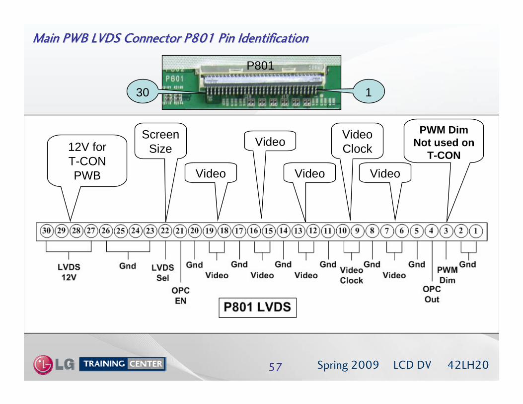
Main PWB LVDS Connector P801 Pin IdentificationMain PWB LVDS Connector P801 Pin Identification
12V forT-CON PWB
PWM Dim Not used on
T-CON
Video
Video
Video
VideoClock
Screen Size
Video
30 1
P801
LCD DV 42LH2058 Spring 2009
0V
0V
0V
0V
Gnd
Gnd
Gnd
Gnd
0V
0V
Gnd
0V
0V
Gnd
0V
SBY
1.6V12.1VLVDS 12V30
1.6V12.1VLVDS 12V29
1.6V12.1VLVDS 12V28
1.6V12.1VLVDS 12V27
GndGndGnd26
GndGndGnd25
GndGndGnd24
GndGndGnd23
Open0VLVDS-SEL22
1.1V0VOPC-EN21
GndGndGnd20
1.1V1.2VTXA0-19
0.8V1.1VTXA0+18
GndGndGnd17
1.1V1.2VTXA1-16
Diode CheckRunLABELPin
Main PWB Connector P801 to TMain PWB Connector P801 to T--CON Voltage and ResistanceCON Voltage and ResistanceDiode Mode values taken with all Connectors Removed
Gnd
Gnd
0V
0V
Gnd
0V
0V
Gnd
0V
0V
Gnd
0V
0V
Gnd
Gnd
SBY
1.1V1.1VTXA1+15
GndGndGnd14
1.1V1.2VTXA2-13
1.1V1.1VTXA2+12
GndGndGnd11
1.1V1.1VTXAC-10
1.1V1.2VTXAC+9
GndGndGnd8
1.1V1.2VTXA3-7
1.1V1.2VTXA3+6
GndGndGnd5
Open3.3VOPC-OUT4
1.1V3.1V*PWM-DIM3
GndGndGnd2
GndGndGnd1
Diode CheckRunLABELPin
P801 CONNECTOR "Main" to CN5 "T-CON PWB"
*Pin 3 PWM-DIM 3.15V (Max 100%) to 0.6V (Min 0%) Customer’s Menu Backlight setting. But is Not Used on T-CON.
LCD DV 42LH2059 Spring 2009
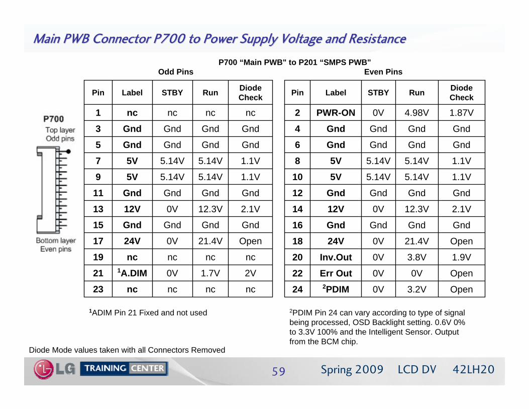
Main PWB Connector P700 to Power Supply Voltage and ResistanceMain PWB Connector P700 to Power Supply Voltage and Resistance
Diode Mode values taken with all Connectors Removed
Open3.2V0V2PDIM24Open0V0VErr Out221.9V3.8V0VInv.Out20Open21.4V0V24V18GndGndGndGnd162.1V12.3V0V12V14GndGndGndGnd121.1V5.14V5.14V5V101.1V5.14V5.14V5V8GndGndGndGnd6GndGndGndGnd4
1.87V4.98V0VPWR-ON2
Diode CheckRun STBYLabelPin
ncncncnc232V1.7V0V1A.DIM21ncncncnc19
Open21.4V0V24V17GndGndGndGnd152.1V12.3V0V12V13GndGndGndGnd111.1V5.14V5.14V5V91.1V5.14V5.14V5V7GndGndGndGnd5GndGndGndGnd3ncncncnc1
Diode CheckRun STBYLabelPin
1ADIM Pin 21 Fixed and not used 2PDIM Pin 24 can vary according to type of signal being processed, OSD Backlight setting. 0.6V 0% to 3.3V 100% and the Intelligent Sensor. Output from the BCM chip.
P700 “Main PWB" to P201 “SMPS PWB"Odd Pins Even Pins
LCD DV 42LH2060 Spring 2009
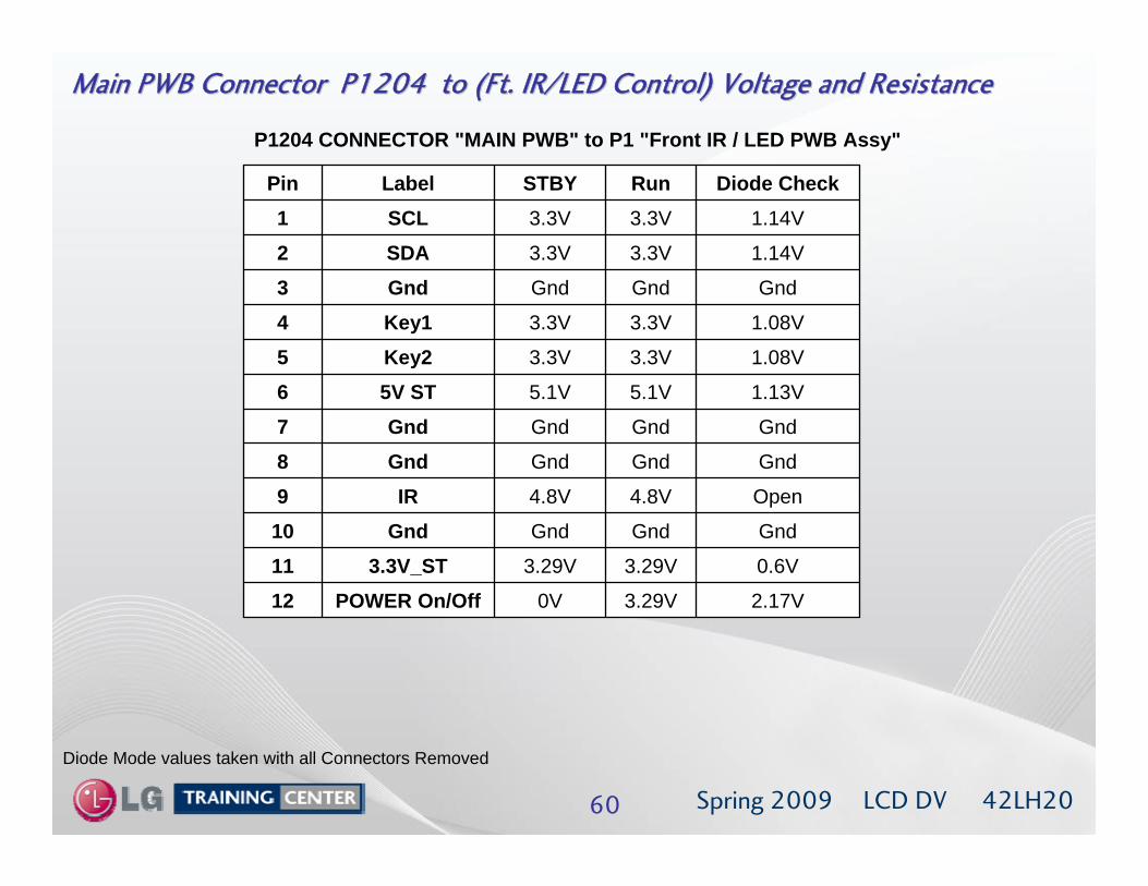
Main PWB Connector P1204 to (Ft. IR/LED Control) Voltage and RMain PWB Connector P1204 to (Ft. IR/LED Control) Voltage and Resistanceesistance
Diode Mode values taken with all Connectors Removed
P1204 CONNECTOR "MAIN PWB" to P1 "Front IR / LED PWB Assy"
2.17V3.29V0VPOWER On/Off120.6V3.29V3.29V3.3V_ST11GndGndGndGnd10
Open4.8V4.8VIR9GndGndGndGnd8GndGndGndGnd7
1.13V5.1V5.1V5V ST61.08V3.3V3.3VKey251.08V3.3V3.3VKey14GndGndGndGnd3
1.14V3.3V3.3VSDA21.14V3.3V3.3VSCL1
Diode CheckRun STBYLabelPin
LCD DV 42LH2061 Spring 2009
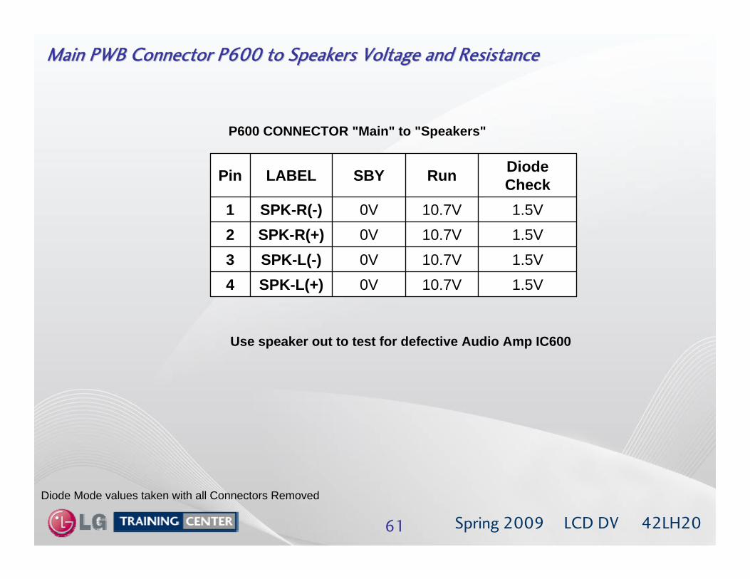
Main PWB Connector P600 to Speakers Voltage and ResistanceMain PWB Connector P600 to Speakers Voltage and Resistance
Diode Mode values taken with all Connectors Removed
SPK-L(+)SPK-L(-)SPK-R(+)SPK-R(-)
LABEL
1.5V10.7V0V41.5V10.7V0V31.5V10.7V0V21.5V10.7V0V1
Diode CheckRunSBYPin
P600 CONNECTOR "Main" to "Speakers"
Use speaker out to test for defective Audio Amp IC600

LCD DV 42LH2062 Spring 2009
Front PWB Assembly (Front PWB Assembly (IRIR and LED Control) Layout (Back View)and LED Control) Layout (Back View)
P1
To Main PWB
To Side Key PWB
The IR Sensor and Power LED control IC are located on the front of this PWB
IR Sensor
Cover
P1
顰顰P3 P1
顰顰
To Main PWB

LCD DV 42LH2063 Spring 2009
IR Sensor
POWER LEDS (LED1 through LED10)
Front PWB Assembly (Front PWB Assembly (IRIR and LED Control) Layout (Back View)and LED Control) Layout (Back View)
Control IC U1 (Power LEDs)

LCD DV 42LH2064 Spring 2009
Front Front IRIR/LED Control Connector P1 and P3 to Main Voltage and Resistance/LED Control Connector P1 and P3 to Main Voltage and Resistance
Diode Mode values taken with all Connectors Removed
2V
Open
Gnd
2V
Gnd
Gnd
1.5V
Open
Open
Gnd
2.4V
2.4V
Diode Check
3.3V3.3VSCL13.3V3.3VSDA2GndGndGnd33.3V3.3VKey143.3V3.3VKey255.1V5.1V5V ST6GndGndGnd7GndGndGnd84.8V4.8VIR9GndGndGnd10
3.29V3.29V3.3V_ST113.29V0VPOWER On/Off12
RunSTBYLABELPin
P1 Connector “IR/LED Control PWB“to "MAIN PWB" P404
P3 Connector “IR/LED Control PWB“to “Side Key" P3000
Gnd
Key2
Gnd
Key1
Label
Gnd
Open
Gnd
Open
Diode Check
GndGnd4
3.3V3.3V3
GndGnd2
3.3V3.3V1
Run STBYPin
LCD DV 42LH2065 Spring 2009
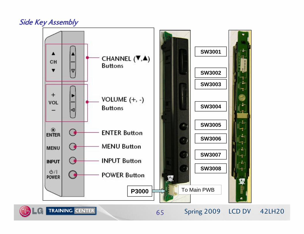
Side Key AssemblySide Key Assembly
To Main PWB
顰
P3000
SW3008
SW3007
SW3006
SW3005
SW3004
SW3003
SW3002
SW3001
顰
PWM-DIM (PWM Dimming) Manipulates the Backlight Brightness via Customer’s OSD.Manipulates the Backlight Brightness via the BCM Chip. Darker Picture, Darker Backlights to facilitate improved Contrast Ratio. 0.6V ~ 3.3V Range
42LH20 P700 ON MAIN PWB TO SMPS P201 TURN ON CIRCUIT
R189
R185
1.2K
INV ON/OFF
PWR ON
100
R714
R704
C711150pF
C1811uF
P700
12V12V
Gnd
Gnd
Gnd
Gnd
0V
3.38V
4.98V
1.8V
PWR On
P201
ERR Out
PWR
A.DIMINV.On
PWM-DIM
n/c
SMPS
AB12
IC100BCM
PWM2
PWM0
100
n/c
GndGndGndGnd
A-DIM (Analog Dimming) Fixed Value.
100
H5R245100
GPIO137SBY5V
MAINPWB
5V
5V5V5V
GndGnd
12V
2
1
4
3
6
5
8
7
10
9
11
12
14
13
16
15
18
17
20
19
22
21
23
24
2
1
4
3
6
5
8
7
10
9
11
12
14
13
16
15
18
17
20
19
22
21
23
24
21.3V24V
GndGnd
GndGndGndGnd
n/c n/c
n/c n/c
E5 GPIO 134L706
L70424V
C72168uF
C72768uF
L70712V
C7200.1uF C722
47uF
L701Q701
R703R706
R237
G5R719 1KΩ
Q702
R759 0Ω
R717 3.3KΩ
GPIO 136R244 100Ω
+5V General
Power On
Inverter On/Off
3
1
2
6
5
8
7
Q706
+5VL715
+5V GeneralL714
LVDS 12V Panel PowerL728
Q703 R237 100Ω
0.2V
6V
0.6V
4Q704Q705
LVDS Panel Control
L708
R25310KΩ
0V0.6V
12VR739 47KΩ
R740 47KΩ
AB13
PWM-DIM (Digital Dimming)
C726220uF STBY5V
L700
R743
0
L733
Relay On
A-DIM
P-DIM
STBY5V
STBY5V
4.7K C1821uF
C7251uF
C7061uF
21.3V
3.8V
10K10K
PG26
LCD DV 42LH2067 Spring 2009
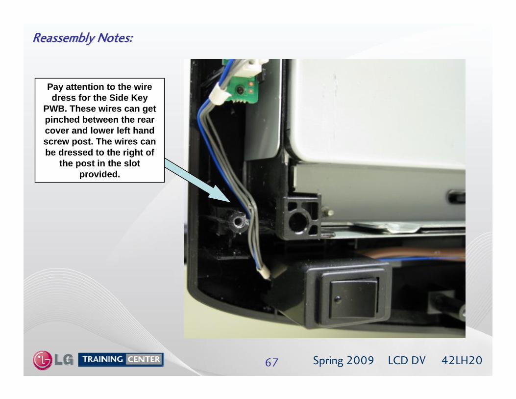
Reassembly Notes:Reassembly Notes:
Pay attention to the wire dress for the Side Key
PWB. These wires can get pinched between the rear cover and lower left hand screw post. The wires can be dressed to the right of
the post in the slot provided.
LCD DV 42LH2068 Spring 2009
11 X 17 Foldout Section11 X 17 Foldout Section
This section shows the 11X17 foldout thatThis section shows the 11X17 foldout that’’s available in the Paper s available in the Paper and Adobe version of the Training Manual.and Adobe version of the Training Manual.
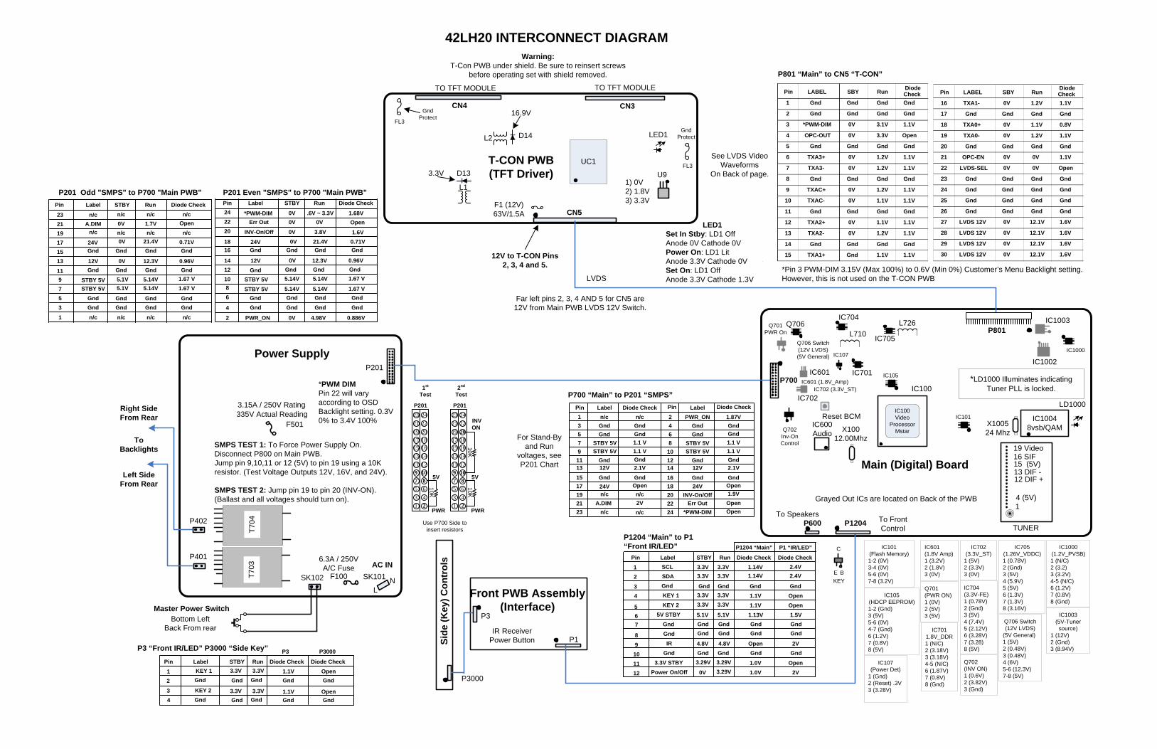
42LH20 INTERCONNECT DIAGRAM
X100524 Mhz
P700
P3
P1
Power Supply
Main (Digital) Board
Front PWB Assembly(Interface)
Side
(Key
) Con
trol
s
P600
P201
F501
F100 SK101
LN
6.3A / 250VA/C Fuse
335V Actual Reading3.15A / 250V Rating
IR ReceiverPower Button
To Speakers
P3000
Reset BCM
P801
IC100
63V/1.5A
CN4 CN3
TO TFT MODULE
SMPS TEST 1: To Force Power Supply On.Disconnect P800 on Main PWB.Jump pin 9,10,11 or 12 (5V) to pin 19 using a 10K resistor. (Test Voltage Outputs 12V, 16V, and 24V).
SMPS TEST 2: Jump pin 19 to pin 20 (INV-ON).(Ballast and all voltages should turn on).
IC10048vsb/QAMX100
12.00Mhz
LVDS
IC600Audio
Grayed Out ICs are located on Back of the PWB
16 SIF
1
19 Video
4 (5V)
*LD1000 Illuminates indicating Tuner PLL is locked.
Warning:T-Con PWB under shield. Be sure to reinsert screws
before operating set with shield removed.
UC1
D14
D13
L1
L2
U9
16.9V
1) 0V2) 1.8V3) 3.3V
12V to T-CON Pins 2, 3, 4 and 5.
P1204 “Main” to P1 “Front IR/LED”
*PWM DIMPin 22 will vary according to OSD Backlight setting. 0.3V 0% to 3.4V 100%
F1 (12V)
TO TFT MODULE
CN5
3.3V
LED1
LD1000
L726L710
P1204
IC704
IC705
IC701IC1002
IC1003
IC702
IC601
PinPin
Gnd3.3V STBY
Power On/Off
IRGndGnd
5V STBYKEY 2
GndSDASCLLabel
n/c1V1V0V
0V4.8V
0V5.1V0V
0.13Vn/cn/cGnd3.3VRun
3.29V
5.1V
Gnd
STBY
KEY 1
1.0V1.0V
Open
1.13V1.1V1.1VGnd
1.14VDiode Check
101112
98
765
1
432
Q706
T704
T703
SK102
12 DIF +13 DIF -
TUNER
15 (5V)
T-CON PWB(TFT Driver)
AC IN
Master Power Switch
P401
P402
ToBacklights
IC100Video
ProcessorMstar
Q706 Switch(12V LVDS)(5V General)
IC601 (1.8V_Amp)
IC101
IC105
IC1000
Q702Inv-On Control
IC107
3.29V3.29VGnd Gnd Gnd
Gnd GndGnd Gnd
GndGnd
Gnd
3.3V3.3V3.3V 1.14V
3.3V 3.3V3.3V 3.3V
4.8V
Open2V
2V
1.5VOpenOpenGnd
2.4VDiode Check
Gnd
GndGnd
P1204 “Main” P1 “IR/LED”
2.4V
P3 “Front IR/LED” P3000 “Side Key”Pin
Gnd
Label Run STBY
Gnd
Diode Check1
432 Gnd Gnd
Diode Check
P3 P3000
KEY 1 1.1V3.3V Open3.3VGnd
Gnd GndGnd GndKEY 2 1.1V3.3V Open3.3V
Gnd
To Front Control
PWR_ONGndGnd
Gnd12VGnd24V
INV-On/Off
*PWM-DIM
Labeln/cGndGnd
STBY 5V
Gnd12VGnd
A.DIMn/c
STBY 5V
Err Out
STBY 5VSTBY 5V
LabelPin
2468
1012141618202224
Pin1357911131517192123
Diode Check
Gnd
Gnd
1.87V
Open
Diode Check
Gnd
Gnd
Gnd
Open
n/c
n/c
n/c
Gnd
GndGnd
2.1V
1.1 V1.1 V
1.9V
Open2V
24Vn/c
Open
2.1V
1.1 V1.1 V
P700 “Main” to P201 “SMPS”
For Stand-By and Run
voltages, see P201 Chart
Pin LABEL SBY Run
1 Gnd Gnd Gnd Gnd
2 Gnd Gnd Gnd Gnd
3 *PWM-DIM 0V 3.1V 1.1V
4 OPC-OUT 0V 3.3V Open
5 Gnd Gnd Gnd Gnd
6 TXA3+ 0V 1.2V 1.1V
7 TXA3- 0V 1.2V 1.1V
8 Gnd Gnd Gnd Gnd
9 TXAC+ 0V 1.2V 1.1V
10 TXAC- 0V 1.1V 1.1V
11 Gnd Gnd Gnd Gnd
12 TXA2+ 0V 1.1V 1.1V
13 TXA2- 0V 1.2V 1.1V
14 Gnd Gnd Gnd Gnd
15 TXA1+ Gnd 1.1V 1.1V
Pin LABEL SBY RunDiode Check
16 TXA1- 0V 1.2V 1.1V
17 Gnd Gnd Gnd Gnd
18 TXA0+ 0V 1.1V 0.8V
19 TXA0- 0V 1.2V 1.1V
20 Gnd Gnd Gnd Gnd
21 OPC-EN 0V 0V 1.1V
22 LVDS-SEL 0V 0V Open
23 Gnd Gnd Gnd Gnd
24 Gnd Gnd Gnd Gnd
25 Gnd Gnd Gnd Gnd
26 Gnd Gnd Gnd Gnd
27 LVDS 12V 0V 12.1V 1.6V
28 LVDS 12V 0V 12.1V 1.6V
29 LVDS 12V 0V 12.1V 1.6V
30 LVDS 12V 0V 12.1V 1.6V
Diode Check
P801 “Main” to CN5 “T-CON”
Left SideFrom Rear
Right SideFrom Rear
P201 Odd "SMPS" to P700 "Main PWB"Pin Label STBY Run Diode Check
1 n/c3 Gnd Gnd Gnd Gnd5 Gnd7 STBY 5V9
5.14V
11 Gnd5.14V
13 12V15 Gnd Gnd Gnd Gnd17 24V 0V 21.4V19 n/c21 A.DIM 0V 1.7V23 n/c
5.1V5.1V
Gnd
0.71V
STBY 5V
n/c n/c n/c
n/c n/c n/c
Gnd Gnd
n/c n/c n/c
0V
Gnd Gnd Gnd
0.96V
1.67 V1.67 V
12.3V
Open
P201 Even "SMPS" to P700 "Main PWB"Pin Label STBY Run Diode Check
2 PWR_ON 0V
4 Gnd Gnd Gnd Gnd
6 Gnd
810
5.14V 5.14V
12 Gnd5.14V 5.14V
14 12V
16 Gnd Gnd Gnd Gnd18 24V 0V
20 INV-On/Off 0V 3.8V
22*PWM-DIM
0V
24 0V .6V ~ 3.3V
4.98V
1.67 V
0.886V
OpenErr Out
STBY 5VSTBY 5V
0V 12.3VGndGnd Gnd
Gnd Gnd Gnd
1.67 V
0.96V
21.4V 0.71V1.6V
1.68V0V
Bottom LeftBack From rear
P201
42
86
1210
1614
2018
22
31
75
119
1513
1917
212423
10K
PWR
5V
P201
42
86
22
31
75
119
1513
1917
212423
10K
PWR
5V
10K
1210
1614
2018
INVON
Use P700 Side to insert resistors
1st
Test2nd
Test
FL3
GndProtect
FL3
GndProtect
Far left pins 2, 3, 4 AND 5 for CN5 are 12V from Main PWB LVDS 12V Switch.
LED1Set In Stby: LD1 OffAnode 0V Cathode 0VPower On: LD1 LitAnode 3.3V Cathode 0VSet On: LD1 OffAnode 3.3V Cathode 1.3V
Q701PWR On
IC702 (3.3V_ST)
Q706 Switch(12V LVDS)
(5V General)1 (5V)2 (0.48V)3 (0.48V)4 (6V)5-6 (12.3V)7-8 (5V)
IC704(3.3V-FE)1 (0.78V)2 (Gnd)3 (5V)4 (7.4V)5 (2.12V)6 (3.28V)7 (3.28)8 (5V)
IC705(1.26V_VDDC)1 (0.78V)2 (Gnd)3 (5V)4 (5.9V)5 (5V)6 (1.3V)7 (1.3V)8 (3.16V)
IC7011.8V_DDR1 (N/C)2 (3.18V)3 (3.18V)4-5 (N/C)6 (1.87V)7 (0.8V)8 (Gnd)
IC1000(1.2V_PVSB)1 (N/C)2 (3.2)3 (3.2V)4-5 (N/C)6 (1.2V)7 (0.8V)8 (Gnd)
IC105(HDCP EEPROM)1-2 (Gnd)3 (5V)5-6 (0V)4-7 (Gnd)6 (1.2V)7 (0.8V)8 (5V)
IC101(Flash Memory)1-2 (0V)3-4 (0V)5-6 (0V)7-8 (3.2V)
IC1003(5V-Tuner
source)1 (12V)2 (Gnd)3 (8.94V)
IC702 (3.3V_ST)
1 (5V)2 (3.3V)3 (0V)
IC601(1.8V Amp)1 (3.2V)2 (1.8V)3 (0V)
IC107(Power Det)
1 (Gnd)2 (Reset) .3V3 (3.28V)
Q701(PWR ON)1 (0V)2 (5V)3 (5V)
Q702(INV ON)1 (0.6V)2 (3.82V)3 (Gnd)
B
C
EKEY
*Pin 3 PWM-DIM 3.15V (Max 100%) to 0.6V (Min 0%) Customer’s Menu Backlight setting.However, this is not used on the T-CON PWB
See LVDS Video Waveforms
On Back of page.
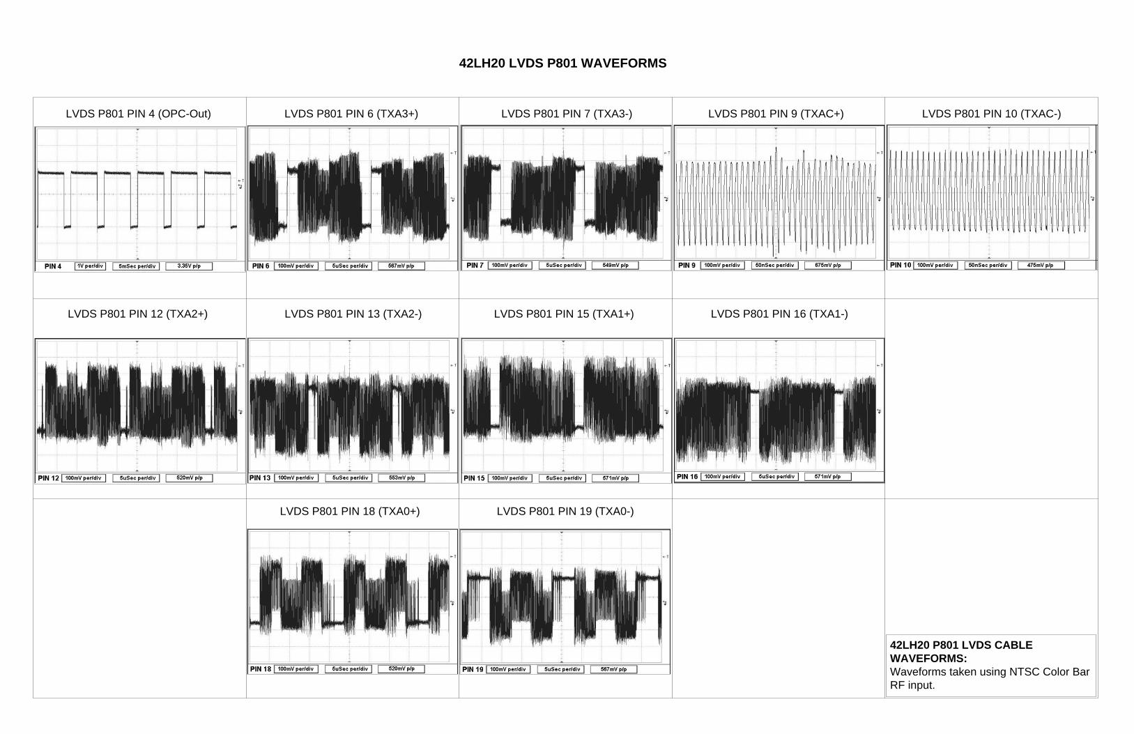
42LH20 LVDS P801 WAVEFORMS
42LH20 P801 LVDS CABLE WAVEFORMS:Waveforms taken using NTSC Color Bar RF input.
LVDS P801 PIN 4 (OPC-Out) LVDS P801 PIN 6 (TXA3+) LVDS P801 PIN 7 (TXA3-) LVDS P801 PIN 9 (TXAC+) LVDS P801 PIN 10 (TXAC-)
LVDS P801 PIN 12 (TXA2+) LVDS P801 PIN 13 (TXA2-) LVDS P801 PIN 15 (TXA1+) LVDS P801 PIN 16 (TXA1-)
LVDS P801 PIN 18 (TXA0+) LVDS P801 PIN 19 (TXA0-)