
4-Port Hub for the Universal Serial Bus w/optional Serial ... · DP1–DP4 paired with DM1–DM4...
29
Personal Computer Monitor with TUSB2046B 4-Port Hub Modem Scanner Digital Scanner Right Speaker Mouse Left Speaker Printer with TUSB2046B 4-Port Hub Keyboard with TUSB2046B 4-Port Hub ... ... ... Product Folder Order Now Technical Documents Tools & Software Support & Community An IMPORTANT NOTICE at the end of this data sheet addresses availability, warranty, changes, use in safety-critical applications, intellectual property matters and other important disclaimers. PRODUCTION DATA. TUSB2046B, TUSB2046I SLLS413L – FEBRUARY 2000 – REVISED JUNE 2017 TUSB2046x 4-Port Hub for the Universal Serial Bus With Optional Serial EEPROM Interface 1 (1) JEDEC descriptor S-PQFP-G for low-profile quad flatpack (LQFP). 1 Features 1• Fully Compliant With the USB Specification as a Full-Speed Hub: TID #30220231 • 32-Pin LQFP (1) Package With a 0.8-mm Terminal Pitch or QFN Package With a 0.5-mm Pin Pitch • 3.3-V Low-Power ASIC Logic • Integrated USB Transceivers • State Machine Implementation Requires No Firmware Programming • One Upstream Port and Four Downstream Ports • All Downstream Ports Support Full-Speed and Low-Speed Operations • Two Power Source Modes – Self-Powered Mode – Bus-Powered Mode • Power Switching and Overcurrent Reporting Is Provided Ganged or Per Port • Supports Suspend and Resume Operations • Supports Programmable Vendor ID and Product ID With External Serial EEPROM • 3-State EEPROM Interface Allows EEPROM Sharing • Push-Pull Outputs for PWRON Eliminate the Need for External Pullup Resistors • Noise Filtering on OVRCUR Provides Immunity to Voltage Spikes • Package Pinout Allows 2-Layer PCB • Low EMI Emission Achieved by a 6-MHz Crystal Input • Migrated From Proven TUSB2040 Hub • Lower Cost Than the TUSB2040 Hub • Enhanced System ESD Performance • No Special Driver Requirements; Works Seamlessly With Any Operating System With USB Stack Support • Supports 6-MHz Operation Through a Crystal Input or a 48-MHz Input Clock 2 Applications • Computer Systems • Docking Stations 3 Description The TUSB2046x is a 3.3-V CMOS hub device that provides one upstream port and four downstream ports in compliance with the Universal Serial Bus (USB) specification as a full-speed hub. Because this device is implemented with a digital state machine instead of a microcontroller, no firmware programming is required. Fully compliant USB transceivers are integrated into the ASIC for all upstream and downstream ports. The downstream ports support full-speed and low-speed devices by automatically setting the slew rate according to the speed of the device attached to the ports. The configuration of the BUSPWR pin selects either the bus-powered or the self-powered mode. Configuring the GANGED input determines the power switching and overcurrent detection modes for the downstream ports. If GANGED is high, all PWRON outputs switch together and if any OVRCUR is activated, all ports transition to the power-off state. If GANGED is low, the PWRON outputs and OVRCUR inputs operate on a per-port basis. Device Information (1) PART NUMBER PACKAGE BODY SIZE (NOM) TUSB2046B TUSB2046BI TUSB2046I VQFN (32) 5.00 mm × 5.00 mm LQFP (32) 7.00 mm × 7.00 mm (1) For all available packages, see the orderable addendum at the end of the data sheet. USB-Tiered Configuration Example
Transcript of 4-Port Hub for the Universal Serial Bus w/optional Serial ... · DP1–DP4 paired with DM1–DM4...

PersonalComputer
Monitor withTUSB2046B4-Port Hub Modem
Scanner
Digital Scanner
Right Speaker
Mouse
Left Speaker
Printer withTUSB2046B4-Port Hub
Keyboard withTUSB2046B4-Port Hub ...
...
...
Product
Folder
Order
Now
Technical
Documents
Tools &
Software
Support &Community
An IMPORTANT NOTICE at the end of this data sheet addresses availability, warranty, changes, use in safety-critical applications,intellectual property matters and other important disclaimers. PRODUCTION DATA.
TUSB2046B, TUSB2046ISLLS413L –FEBRUARY 2000–REVISED JUNE 2017
TUSB2046x 4-Port Hub for the Universal Serial Bus With OptionalSerial EEPROM Interface
1
(1) JEDEC descriptor S-PQFP-G for low-profile quad flatpack(LQFP).
1 Features1• Fully Compliant With the USB Specification as a
Full-Speed Hub: TID #30220231• 32-Pin LQFP (1) Package With a 0.8-mm Terminal
Pitch or QFN Package With a 0.5-mm Pin Pitch• 3.3-V Low-Power ASIC Logic• Integrated USB Transceivers• State Machine Implementation Requires No
Firmware Programming• One Upstream Port and Four Downstream Ports• All Downstream Ports Support Full-Speed and
Low-Speed Operations• Two Power Source Modes
– Self-Powered Mode– Bus-Powered Mode
• Power Switching and Overcurrent Reporting IsProvided Ganged or Per Port
• Supports Suspend and Resume Operations• Supports Programmable Vendor ID and Product
ID With External Serial EEPROM• 3-State EEPROM Interface Allows EEPROM
Sharing• Push-Pull Outputs for PWRON Eliminate the Need
for External Pullup Resistors• Noise Filtering on OVRCUR Provides Immunity to
Voltage Spikes• Package Pinout Allows 2-Layer PCB• Low EMI Emission Achieved by a 6-MHz Crystal
Input• Migrated From Proven TUSB2040 Hub• Lower Cost Than the TUSB2040 Hub• Enhanced System ESD Performance• No Special Driver Requirements; Works
Seamlessly With Any Operating System With USBStack Support
• Supports 6-MHz Operation Through a CrystalInput or a 48-MHz Input Clock
2 Applications• Computer Systems• Docking Stations
3 DescriptionThe TUSB2046x is a 3.3-V CMOS hub device thatprovides one upstream port and four downstreamports in compliance with the Universal Serial Bus(USB) specification as a full-speed hub. Because thisdevice is implemented with a digital state machineinstead of a microcontroller, no firmwareprogramming is required. Fully compliant USBtransceivers are integrated into the ASIC for allupstream and downstream ports. The downstreamports support full-speed and low-speed devices byautomatically setting the slew rate according to thespeed of the device attached to the ports. Theconfiguration of the BUSPWR pin selects either thebus-powered or the self-powered mode.
Configuring the GANGED input determines the powerswitching and overcurrent detection modes for thedownstream ports. If GANGED is high, all PWRONoutputs switch together and if any OVRCUR isactivated, all ports transition to the power-off state. IfGANGED is low, the PWRON outputs and OVRCURinputs operate on a per-port basis.
Device Information(1)
PART NUMBER PACKAGE BODY SIZE (NOM)TUSB2046BTUSB2046BITUSB2046I
VQFN (32) 5.00 mm × 5.00 mm
LQFP (32) 7.00 mm × 7.00 mm
(1) For all available packages, see the orderable addendum atthe end of the data sheet.
USB-Tiered Configuration Example

2
TUSB2046B, TUSB2046ISLLS413L –FEBRUARY 2000–REVISED JUNE 2017 www.ti.com
Product Folder Links: TUSB2046B TUSB2046I
Submit Documentation Feedback Copyright © 2000–2017, Texas Instruments Incorporated
Table of Contents1 Features .................................................................. 12 Applications ........................................................... 13 Description ............................................................. 14 Revision History..................................................... 25 Description (Continued) ........................................ 36 Pin Configuration and Functions ......................... 47 Specifications......................................................... 6
7.1 Absolute Maximum Ratings ..................................... 67.2 ESD Ratings.............................................................. 67.3 Recommended Operating Conditions....................... 67.4 Thermal Information .................................................. 77.5 Electrical Characteristics........................................... 77.6 Differential Driver Switching Characteristics (Full
Speed Mode) ............................................................. 77.7 Differential Driver Switching Characteristics (Low
Speed Mode) ............................................................. 87.8 Typical Characteristics .............................................. 9
8 Detailed Description .............................................. 98.1 Overview ................................................................... 98.2 Functional Block Diagram ....................................... 10
8.3 Feature Description................................................. 108.4 Device Functional Modes........................................ 128.5 Programming........................................................... 13
9 Application and Implementation ........................ 159.1 Application Information............................................ 159.2 Typical Application .................................................. 15
10 Power Supply Recommendations ..................... 1710.1 TUSB2046x Power Supply ................................... 1710.2 Downstream Port Power ....................................... 17
11 Layout................................................................... 1811.1 Layout Guidelines ................................................. 1811.2 Layout Example .................................................... 19
12 Device and Documentation Support ................. 2012.1 Related Links ........................................................ 2012.2 Community Resources.......................................... 2012.3 Trademarks ........................................................... 2012.4 Electrostatic Discharge Caution............................ 2012.5 Glossary ................................................................ 20
13 Mechanical, Packaging, and OrderableInformation ........................................................... 20
4 Revision HistoryNOTE: Page numbers for previous revisions may differ from page numbers in the current version.
Changes from Revision K (January 2016) to Revision L Page
• Added device TUSB2046IB to the data sheet........................................................................................................................ 1
Changes from Revision J (July 2015) to Revision K Page
• Changed the VQFN package Body Size From: 5.00 mm x 2.00 mm To: 5.00 mm x 5.00 mm ............................................ 1
Changes from Revision I (September 2013) to Revision J Page
• Added Pin Configuration and Functions section, ESD Ratings table, Feature Description section, Device FunctionalModes, Application and Implementation section, Power Supply Recommendations section, Layout section, Deviceand Documentation Support section, and Mechanical, Packaging, and Orderable Information section .............................. 1

3
TUSB2046B, TUSB2046Iwww.ti.com SLLS413L –FEBRUARY 2000–REVISED JUNE 2017
Product Folder Links: TUSB2046B TUSB2046I
Submit Documentation FeedbackCopyright © 2000–2017, Texas Instruments Incorporated
5 Description (Continued)The TUSB2046x provides the flexibility of using a 6-MHz or a 48-MHz clock. The logic level of the TSTMODEterminal controls the selection of the clock source. When TSTMODE is low, the output of the internal APLLcircuitry is selected to drive the internal core of the device. When TSTMODE is high, the TSTPLL/48MCLK inputis selected as the input clock source and the APLL circuitry is powered down and bypassed. The internaloscillator cell is also powered down while TSTMODE is high. Low EMI emission is achieved because theTUSB2046x can usee a 6-MHz crystal input. Connect the crystal as shown in Figure 6. An internal PLL thengenerates the 48-MHz clock used to sample data from the upstream port and to synchronize the 12 MHz usedfor the USB clock. If low-power suspend and resume are desired, a passive crystal or resonator must be used.However, a 6-MHz oscillator may be used by connecting the output to the XTAL1 pin and leaving the XTAL2 pinopen. The oscillator TTL output must not exceed 3.6 V.
For 48-MHz operation, the clock cannot be generated with a crystal using the XTAL2 output because the internaloscillator cell supports only the fundamental frequency. Other useful features of the TUSB2046x include apackage with a 0.8-mm pin pitch for easy PCB routing and assembly, push-pull outputs for the PWRON pinseliminate the need for pullup resistors required by traditional open-collector I/Os, and OVRCUR pins have noisefiltering for increased immunity to voltage spikes.
4
TUSB2046B, TUSB2046ISLLS413L –FEBRUARY 2000–REVISED JUNE 2017 www.ti.com
Product Folder Links: TUSB2046B TUSB2046I
Submit Documentation Feedback Copyright © 2000–2017, Texas Instruments Incorporated
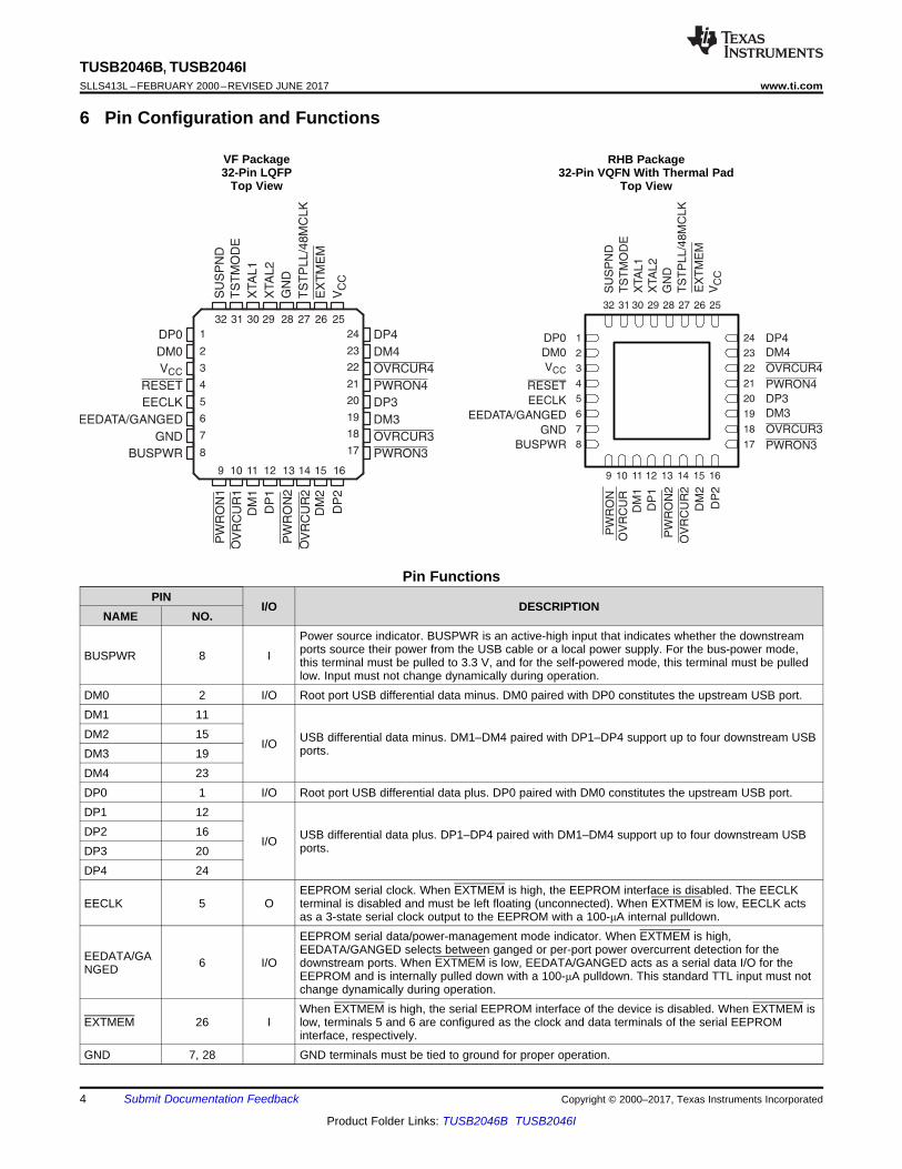
6 Pin Configuration and Functions
VF Package32-Pin LQFP
Top View
RHB Package32-Pin VQFN With Thermal Pad
Top View
Pin FunctionsPIN
I/O DESCRIPTIONNAME NO.
BUSPWR 8 I
Power source indicator. BUSPWR is an active-high input that indicates whether the downstreamports source their power from the USB cable or a local power supply. For the bus-power mode,this terminal must be pulled to 3.3 V, and for the self-powered mode, this terminal must be pulledlow. Input must not change dynamically during operation.
DM0 2 I/O Root port USB differential data minus. DM0 paired with DP0 constitutes the upstream USB port.DM1 11
I/O USB differential data minus. DM1–DM4 paired with DP1–DP4 support up to four downstream USBports.
DM2 15DM3 19DM4 23DP0 1 I/O Root port USB differential data plus. DP0 paired with DM0 constitutes the upstream USB port.DP1 12
I/O USB differential data plus. DP1–DP4 paired with DM1–DM4 support up to four downstream USBports.
DP2 16DP3 20DP4 24
EECLK 5 OEEPROM serial clock. When EXTMEM is high, the EEPROM interface is disabled. The EECLKterminal is disabled and must be left floating (unconnected). When EXTMEM is low, EECLK actsas a 3-state serial clock output to the EEPROM with a 100-μA internal pulldown.
EEDATA/GANGED 6 I/O
EEPROM serial data/power-management mode indicator. When EXTMEM is high,EEDATA/GANGED selects between ganged or per-port power overcurrent detection for thedownstream ports. When EXTMEM is low, EEDATA/GANGED acts as a serial data I/O for theEEPROM and is internally pulled down with a 100-μA pulldown. This standard TTL input must notchange dynamically during operation.
EXTMEM 26 IWhen EXTMEM is high, the serial EEPROM interface of the device is disabled. When EXTMEM islow, terminals 5 and 6 are configured as the clock and data terminals of the serial EEPROMinterface, respectively.
GND 7, 28 GND terminals must be tied to ground for proper operation.

5
TUSB2046B, TUSB2046Iwww.ti.com SLLS413L –FEBRUARY 2000–REVISED JUNE 2017
Product Folder Links: TUSB2046B TUSB2046I
Submit Documentation FeedbackCopyright © 2000–2017, Texas Instruments Incorporated
Pin Functions (continued)PIN
I/O DESCRIPTIONNAME NO.
OVRCUR1 10
I
Overcurrent input. OVRCUR1–OVRCUR4 are active low. For per-port overcurrent detection, oneovercurrent input is available for each of the four downstream ports. In the ganged mode, anyOVRCUR input may be used and all OVRCUR terminals must be tied together. OVRCURterminals are active low inputs with noise filtering logic.
OVRCUR2 14OVRCUR3 18OVRCUR4 22PWRON1 9
O
Power-on/-off control signals. PWRON1–PWRON4 are active low, push-pull outputs. Push-pulloutputs eliminate the pullup resistors which open-drain outputs require. However, the externalpower switches that connect to these terminals must be able to operate with 3.3-V inputs becausethese outputs cannot drive 5-V signals.
PWRON2 13PWRON3 17PWRON4 21
RESET 4 I
RESET is an active low TTL input with hysteresis and must be asserted at power up. WhenRESET is asserted, all logic is initialized. Generally, a reset with a pulse width between 100 μsand 1 ms is recommended after 3.3-V VCC reaches its 90%. Clock signal has to be active duringthe last 60 μs of the reset window.
SUSPND 32 O Suspend status. SUSPND is an active high output available for external logic power-downoperations. During the suspend mode, SUSPND is high. SUSPND is low for normal operation.
TSTMODE 31 I Test/mode terminal. TSTMODE is used as a test terminal during production testing. This terminalmust be tied to ground or 3.3-V VCC for normal 6-MHz or 48-MHz operation, respectively.
TSTPLL/48MCLK 27 I/O
Test/48-MHz clock input. TSTPLL/48MCLK is used as a test terminal during production testing.This terminal must be tied to ground for normal 6-MHz operation. If 48-MHz input clock is desired,a 48-MHz clock source (no crystal) can be connected to this input terminal.
VCC 3, 25 3.3-V supply voltage
XTAL1 30 I Crystal 1. XTAL1 is a 6-MHz crystal input with 50% duty cycle. An internal PLL generates the 48-MHz and 12-MHz clocks used internally by the ASIC logic.
XTAL2 29 O Crystal 2. XTAL2 is a 6-MHz crystal output. This terminal must be left open when using anoscillator.

6
TUSB2046B, TUSB2046ISLLS413L –FEBRUARY 2000–REVISED JUNE 2017 www.ti.com
Product Folder Links: TUSB2046B TUSB2046I
Submit Documentation Feedback Copyright © 2000–2017, Texas Instruments Incorporated
(1) Stresses beyond those listed under Absolute Maximum Ratings may cause permanent damage to the device. These are stress ratingsonly, and functional operation of the device at these or any other conditions beyond those indicated under Recommended OperatingConditions is not implied. Exposure to absolute-maximum-rated conditions for extended periods may affect device reliability.
(2) All voltage levels are with respect to GND.
7 Specifications
7.1 Absolute Maximum Ratingsover operating free-air temperature range (unless otherwise noted) (1)
MIN MAX UNITVCC Supply voltage (2) –0.5 3.6 VVI Input voltage range –0.5 VCC + 0.5 VVO Output voltage range –0.5 VCC + 0.5 VIIK Input clamp current VI < 0 V or VI < VCC ±20 mAIOK Output clamp current VO < 0 V or VO < VCC ±20 mA
TA Operating free-air temperatureTUSB2046B 0 70
°CTUSB2046BI, TUSB2046I –40 85
Tstg Storage temperature range –65 150 °C
(1) JEDEC document JEP155 states that 500-V HBM allows safe manufacturing with a standard ESD control process.(2) JEDEC document JEP157 states that 250-V CDM allows safe manufacturing with a standard ESD control process.
7.2 ESD RatingsVALUE UNIT
V(ESD) Electrostatic dischargeHuman body model (HBM), per ANSI/ESDA/JEDEC JS-001 (1) ±4000
VCharged-device model (CDM), per JEDEC specification JESD22-C101 (2) ±1500
7.3 Recommended Operating ConditionsPARAMETER MIN NOM MAX UNIT
VCC Supply voltageTUSB2046B 3 3.3 3.6
VTUSB2046BI, TUSB2046I 3.3 3.6
VI Input voltage, TTL/LVCMOS 0 VCC VVO Output voltage, TTL/LVCMOS 0 VCC VVIH(REC) High-level input voltage, signal-ended receiver 2 VCC VVIL(REC) Low-level input voltage, signal-ended receiver 0.8 VVIH(TTL) High-level input voltage, TTL/LVCMOS 2 VCC VVIL(TTL) Low-level input voltage, TTL/LVCMOS 0 0.8 V
TA Operating free-air temperatureTUSB2046B 0 70
°CTUSB2046BI, TUSB2046I –40 85
R(DRV) External series, differential driver resistor 22 (–5%) 22 (5%) Ωf(OPRH) Operating (dc differential driver) high speed mode 12 Mb/sf(OPRL) Operating (dc differential driver) low speed mode 1.5 Mb/sVICR Common mode, input range, differential receiver 0.8 2.5 Vtt Input transition times, TTL/LVCMOS 0 25 nsTJ Junction temperature range –40 115 °C
7
TUSB2046B, TUSB2046Iwww.ti.com SLLS413L –FEBRUARY 2000–REVISED JUNE 2017
Product Folder Links: TUSB2046B TUSB2046I
Submit Documentation FeedbackCopyright © 2000–2017, Texas Instruments Incorporated
(1) For more information about traditional and new thermal metrics, see the Semiconductor and IC Package Thermal Metrics applicationreport.
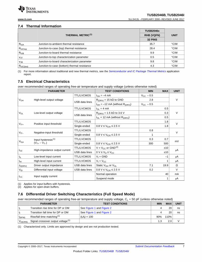
7.4 Thermal Information
THERMAL METRIC (1)TUSB2046x
UNITRHB (VQFN)32 PINS
RθJA Junction-to-ambient thermal resistance 35.7 °C/WRθJCtop Junction-to-case (top) thermal resistance 28.4 °C/WRθJB Junction-to-board thermal resistance 9.9 °C/WψJT Junction-to-top characterization parameter 0.5 °C/WψJB Junction-to-board characterization parameter 9.8 °C/WRθJC(bot) Junction-to-case (bottom) thermal resistance 4.3 °C/W
(1) Applies for input buffers with hysteresis.(2) Applies for open-drain buffers.
7.5 Electrical Characteristicsover recommended ranges of operating free-air temperature and supply voltage (unless otherwise noted)
PARAMETER TEST CONDITIONS MIN MAX UNIT
VOH High-level output voltageTTL/LVCMOS IOH = –4 mA VCC – 0.5
VUSB data lines
R(DRV) = 15 kΩ to GND 2.8IOH = –12 mA (without R(DRV)) VCC – 0.5
VOL Low-level output voltageTTL/LVCMOS IOL = 4 mA 0.5
VUSB data lines
R(DRV) = 1.5 kΩ to 3.6 V 0.3IOL = 12 mA (without R(DRV)) 0.5
VIT+ Positive input thresholdTTL/LVCMOS 1.8
VSingle-ended 0.8 V ≤ VICR ≤ 2.5 V 1.8
VIT– Negative-input thresholdTTL/LVCMOS 0.8
VSingle-ended 0.8 V ≤ VICR ≤ 2.5 V 1
VhysInput hysteresis (1)
(VT+ – VT–)TTL/LVCMOS 0.3 0.7
mVSingle-ended 0.8 V ≤ VICR ≤ 2.5 V 300 500
IOZ High-impedance output currentTTL/LVCMOS V = VCC or GND (2) ±10
μAUSB data lines 0 V ≤ VO ≤ VCC ±10
IIL Low-level input current TTL/LVCMOS VI = GND –1 μAIIH High-level input current TTL/LVCMOS VI = VCC 1 μAz0(DRV) Driver output impedance USB data lines Static VOH or VOL 7.1 19.9 ΩVID Differential input voltage USB data lines 0.8 V ≤ VICR ≤ 2.5 V 0.2 V
ICC Input supply currentNormal operation 40 mASuspend mode 1 μA
(1) Characterized only. Limits are approved by design and are not production tested.
7.6 Differential Driver Switching Characteristics (Full Speed Mode)over recommended ranges of operating free-air temperature and supply voltage, CL = 50 pF (unless otherwise noted)
PARAMETER TEST CONDITIONS MIN MAX UNITtr Transition rise time for DP or DM See Figure 1 and Figure 2 4 20 nstf Transition fall time for DP or DM See Figure 1 and Figure 2 4 20 nst(RFM) Rise/fall time matching (1) (tr/tf) × 100 90% 110%VO(CRS) Signal crossover output voltage (1) 1.3 2.0 V

Vhys
VIT+
VIT-
VCC
VIH
VIL
0 V
Logic high
Logic low
15 kΩ
15 kΩ
1.5 kΩ
22 Ω
22 Ω
8
TUSB2046B, TUSB2046ISLLS413L –FEBRUARY 2000–REVISED JUNE 2017 www.ti.com
Product Folder Links: TUSB2046B TUSB2046I
Submit Documentation Feedback Copyright © 2000–2017, Texas Instruments Incorporated
(1) Characterized only. Limits are approved by design and are not production tested.
7.7 Differential Driver Switching Characteristics (Low Speed Mode)over recommended ranges of operating free-air temperature and supply voltage, CL = 50 pF (unless otherwise noted)
PARAMETER TEST CONDITIONS MIN MAX UNITtr Transition rise time for DP or DM (1) CL = 200 pF to 600 pF, See Figure 1 and Figure 2 75 300 nstf Transition fall time for DP or DM (1) CL = 200 pF to 600 pF, See Figure 1 and Figure 2 75 300 nst(RFM) Rise/fall time matching (1) (tr/tf) × 100 80% 120%VO(CRS) Signal crossover output voltage (1) CL = 200 pF to 600 pF 1.3 2.0 V
Figure 1. Differential Driver Switching Load
Figure 2. Differential Driver Timing Waveforms
Figure 3. Single-Ended Receiver Input Signal Parameter Definitions

0.5
00 1 2
- D
iff
ere
nti
al R
eceiv
er
Inp
ut
Sen
sit
ivit
y -
V
1
1.5
3 4
VID
VICR - Common Mode Input Rang e - V
0.8 3.6
0.2
1.3
2.5
9
TUSB2046B, TUSB2046Iwww.ti.com SLLS413L –FEBRUARY 2000–REVISED JUNE 2017
Product Folder Links: TUSB2046B TUSB2046I
Submit Documentation FeedbackCopyright © 2000–2017, Texas Instruments Incorporated
7.8 Typical Characteristics
Figure 4. Differential Receiver Input Sensitivity vs Common Mode Input Range
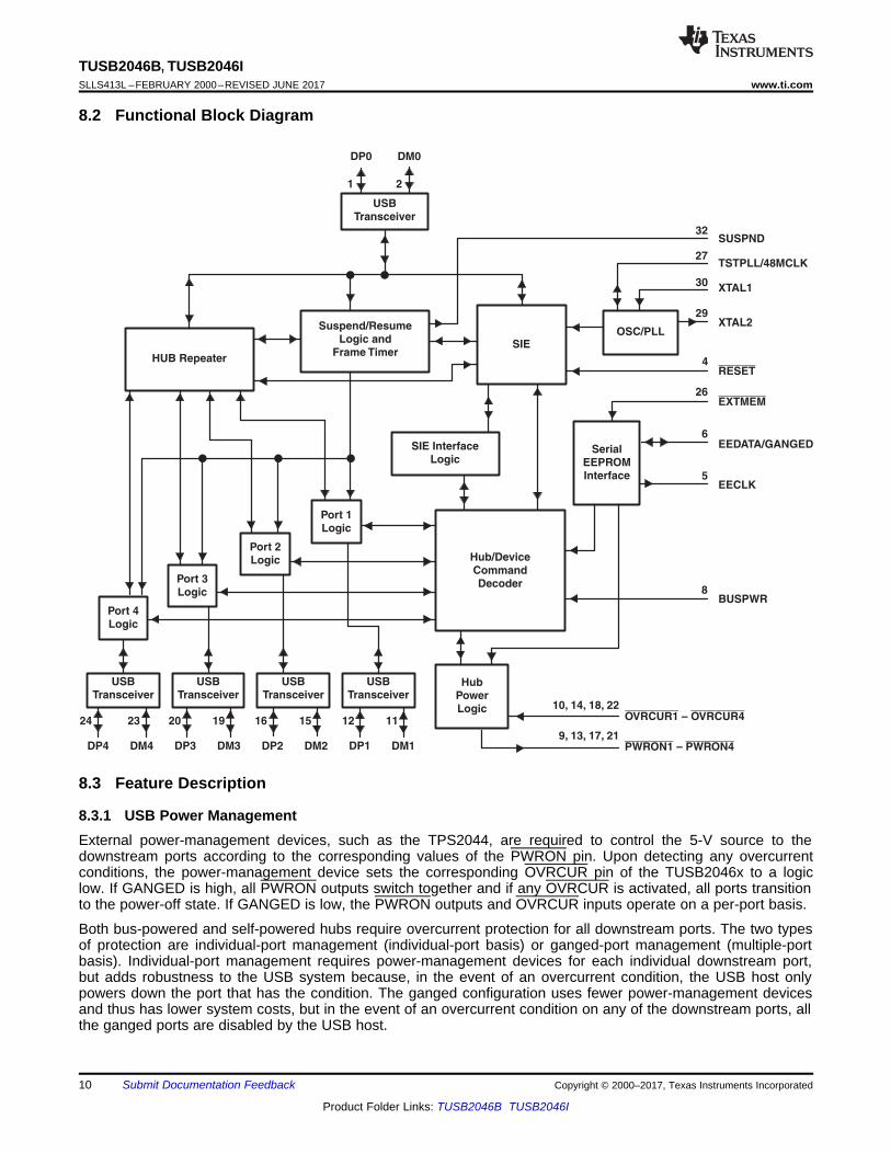
8 Detailed Description
8.1 OverviewThe TUSB2046x is a 3.3-V CMOS hub device that provides one upstream port and four downstream ports incompliance with the Universal Serial Bus (USB) specification as a full-speed hub. Because this device isimplemented with a digital state machine instead of a microcontroller, no firmware programming is required. Fullycompliant USB transceivers are integrated into the ASIC for all upstream and downstream ports. Thedownstream ports support full-speed and low-speed devices by automatically setting the slew rate according tothe speed of the device attached to the ports. The configuration of the BUSPWR pin selects either the bus-powered or the self-powered mode.
SUSPND
XTAL1
XTAL2
RESET
TSTPLL/48MCLK
EEDATA/GANGED
EECLK
10, 14, 18, 22
8
5
6
26
4
29
30
27
32
1 2
24 23 20 19 16 15 12 11
9, 13, 17, 21
BUSPWR
OVRCUR1 OVRCUR4–
PWRON1 PWRON4–
EXTMEM
DP0
DP4 DP3 DP2 DP1
DM0
DM4 DM3 DM2 DM1
USBTransceiver
Suspend/ResumeLogic and
Frame TimerHUB Repeater
SIE
USBTransceiver
USBTransceiver
USBTransceiver
USBTransceiver
OSC/PLL
SerialEEPROMInterface
Hub/DeviceCommandDecoder
Port 4Logic
Port 3Logic
Port 2Logic
Port 1Logic
SIE InterfaceLogic
HubPowerLogic
10
TUSB2046B, TUSB2046ISLLS413L –FEBRUARY 2000–REVISED JUNE 2017 www.ti.com
Product Folder Links: TUSB2046B TUSB2046I
Submit Documentation Feedback Copyright © 2000–2017, Texas Instruments Incorporated
8.2 Functional Block Diagram
8.3 Feature Description
8.3.1 USB Power ManagementExternal power-management devices, such as the TPS2044, are required to control the 5-V source to thedownstream ports according to the corresponding values of the PWRON pin. Upon detecting any overcurrentconditions, the power-management device sets the corresponding OVRCUR pin of the TUSB2046x to a logiclow. If GANGED is high, all PWRON outputs switch together and if any OVRCUR is activated, all ports transitionto the power-off state. If GANGED is low, the PWRON outputs and OVRCUR inputs operate on a per-port basis.
Both bus-powered and self-powered hubs require overcurrent protection for all downstream ports. The two typesof protection are individual-port management (individual-port basis) or ganged-port management (multiple-portbasis). Individual-port management requires power-management devices for each individual downstream port,but adds robustness to the USB system because, in the event of an overcurrent condition, the USB host onlypowers down the port that has the condition. The ganged configuration uses fewer power-management devicesand thus has lower system costs, but in the event of an overcurrent condition on any of the downstream ports, allthe ganged ports are disabled by the USB host.
XTAL1
C1 C2
CL
XTAL2
11
TUSB2046B, TUSB2046Iwww.ti.com SLLS413L –FEBRUARY 2000–REVISED JUNE 2017
Product Folder Links: TUSB2046B TUSB2046I
Submit Documentation FeedbackCopyright © 2000–2017, Texas Instruments Incorporated
Feature Description (continued)Using a combination of the BUSPWR and EEDATA/GANGED inputs, the TUSB2046x supports four modes ofpower management: bus-powered hub with either individual-port power-management or ganged-port powermanagement, and the self-powered hub with either individual-port power management or ganged-port powermanagement. TI supplies the complete hub solution with the TUSB2036 (2/3-port), TUSB2046x, and theTUSB2077 (7-port) hubs along with the power-management devices needed to implement a fully USBspecification-compliant system.
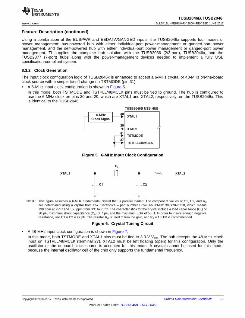
8.3.2 Clock GenerationThe input clock configuration logic of TUSB2046x is enhanced to accept a 6-MHz crystal or 48-MHz on-the-boardclock source with a simple tie-off change on TSTMODE (pin 31).• A 6-MHz input clock configuration is shown in Figure 5.
In this mode, both TSTMODE and TSTPLL/48MCLK pins must be tied to ground. The hub is configured touse the 6-MHz clock on pins 30 and 29, which are XTAL1 and XTAL2, respectively, on the TUSB2046x. Thisis identical to the TUSB2046.
Figure 5. 6-MHz Input Clock Configuration
NOTE: This figure assumes a 6-MHz fundamental crystal that is parallel loaded. The component values of C1, C2, and Rdare determined using a crystal from Fox Electronics – part number HC49U-6.00MHz 30\50\0-70\20, which means±30 ppm at 25°C and ±50 ppm from 0°C to 70°C. The characteristics for the crystal include a load capacitance (CL) of20 pF, maximum shunt capacitance (Co) of 7 pF, and the maximum ESR of 50 Ω. In order to insure enough negativeresistance, use C1 = C2 = 27 pF. The resistor Rd is used to trim the gain, and Rd = 1.5 kΩ is recommended.
Figure 6. Crystal Tuning Circuit
• A 48-MHz input clock configuration is shown in Figure 7.In this mode, both TSTMODE and XTAL1 pins must be tied to 3.3-V VCC. The hub accepts the 48-MHz clockinput on TSTPLL/48MCLK (terminal 27). XTAL2 must be left floating (open) for this configuration. Only theoscillator or the onboard clock source is accepted for this mode. A crystal cannot be used for this mode,because the internal oscillator cell of the chip only supports the fundamental frequency.
Ω
30
29
31
27
XTAL1
XTAL2
TSTMODE
TSTPLL/48MCLK
TUSB2046B USB HUB
Open
48-MHz Oscillator
or on Board Clock Source
3.3 V
12
TUSB2046B, TUSB2046ISLLS413L –FEBRUARY 2000–REVISED JUNE 2017 www.ti.com
Product Folder Links: TUSB2046B TUSB2046I
Submit Documentation Feedback Copyright © 2000–2017, Texas Instruments Incorporated
Feature Description (continued)
Figure 7. 48-MHz Input Clock Configuration
8.4 Device Functional Modes
8.4.1 Vendor ID and Product ID With External Serial EEPROMThe EXTMEM pin enables or disables the optional EEPROM interface. When the EXTMEM pin is high, theproduct ID (PID) displayed during enumeration is the general-purpose USB hub. For this default, pin 5 is disabledand pin 6 functions as the GANGED input pin. If custom product ID (PID) and vendor ID (VID) descriptors aredesired, the EXTMEM pin must be low (EXTMEM = 0). For this configuration, pins 5 and 6 function as theEEPROM interface with pins 5 and 6 functioning as EECLK and EEDATA, respectively. See Table 1 for adescription of the EEPROM memory map. A block diagram example of how to connect the external EEPROM if acustom PID and VID are desired is shown in Figure 8.
Figure 8. Typical Application of the TUSB2046x USB Hub

13
TUSB2046B, TUSB2046Iwww.ti.com SLLS413L –FEBRUARY 2000–REVISED JUNE 2017
Product Folder Links: TUSB2046B TUSB2046I
Submit Documentation FeedbackCopyright © 2000–2017, Texas Instruments Incorporated
8.5 ProgrammingAn SGS Thompson M93C46 EEPROM, or equivalent, stores the programmable VID and PID. When theEEPROM interface is enabled (EXTMEM = 0), the EECLK and EEDATA are internally pulled down (100 μA)inside the TUSB2046x. The internal pulldowns are disabled when the EEPROM interface is disabled(EXTMEM = 1).
The EEPROM is programmed with the three 16-bit locations as shown in Table 1. Connecting terminal 6 of theEEPROM high (ORG = 1) organizes the EEPROM memory into 64×16-bit words.
Table 1. EEPROM Memory MapADDRESS D15 D14 D13 D12–D8 D7–D0
00000 0 GANGED 00000 00000 0000000000001 VID high-byte VID low-byte00010 PID high-byte PID low-byte
XXXXXXXX
The D and Q signals of the EEPROM must be tied together using a 1-kΩ resistor with the common I/Ooperations forming a single-wire bus. After system power-on reset, the TUSB2046x performs a one-time accessread operation from the EEPROM if the EXTMEM terminal is pulled low and the chip select(s) of the EEPROM isconnected to the system power-on reset. Initially, the EEDATA terminal is driven by the TUSB2046x to send astart bit (1) which is followed by the read instruction (10) and the starting-word address (00000). Once the readinstruction is received, the instruction and address are decoded by the EEPROM, which then sends the data tothe output shift register. At this point, the hub stops driving the EEDATA terminal and the EEPROM starts driving.A dummy (0) bit is then output and the first three 16-bit words in the EEPROM are output with the mostsignificant bit (MSB) first.
The output data changes are triggered by the rising edge of the clock provided by the TUSB2046x on the EECLKterminal. The SGS-Thompson M936C46 EEPROM is recommended because it advances to the next memorylocation by automatically incrementing the address internally. Any EEPROM used must have the automaticinternal address advance function. After reading the three words of data from the EEPROM, the TUSB2046xputs the EEPROM interface into a high-impedance condition (pulled down internally) to allow other logic to sharethe EEPROM. The EEPROM read operation is summarized in Figure 9. For more details on EEPROM operation,refer to SGS-Thompson Microelectronics M93C46 Serial Microwire Bus EEPROM data sheet.

6 B
itA
dd
ress (
000000)
Sta
rtR
ead
OP
Co
de(1
0)
48 D
ata
Bit
sD
on
’t C
are
D15
D14
D0
XX
A5
A1
A0
Du
mm
yB
itM
SB
ofT
he
Fir
stW
ord
Oth
er
Data
Bit
sL
SB
of
Th
ird
Wo
rdM
SB
of
Fo
urt
hW
ord
EE
PR
OM
Dri
vin
g D
ata
Lin
eH
ub
Dri
vin
g D
ata
Lin
e
3-S
tate
dW
ith
In
tern
al
Pu
lld
ow
n
S C D
Oth
er
Ad
dre
ss
Bit
s
14
TUSB2046B, TUSB2046ISLLS413L –FEBRUARY 2000–REVISED JUNE 2017 www.ti.com
Product Folder Links: TUSB2046B TUSB2046I
Submit Documentation Feedback Copyright © 2000–2017, Texas Instruments Incorporated
Figure 9. EEPROM Read Operation Timing Diagram
DCPower
TUSB2046B
USBType B
Connector
USB Type AConnector
US Port
DS Port 1 DS Port 2 DS Port 3 DS Port 4
USB Power Switch
USB Power Switch
USB Type AConnector
USB Type AConnector
USB Type AConnector
15
TUSB2046B, TUSB2046Iwww.ti.com SLLS413L –FEBRUARY 2000–REVISED JUNE 2017
Product Folder Links: TUSB2046B TUSB2046I
Submit Documentation FeedbackCopyright © 2000–2017, Texas Instruments Incorporated
9 Application and Implementation
NOTEInformation in the following applications sections is not part of the TI componentspecification, and TI does not warrant its accuracy or completeness. TI’s customers areresponsible for determining suitability of components for their purposes. Customers shouldvalidate and test their design implementation to confirm system functionality.
9.1 Application InformationA major advantage of USB is the ability to connect 127 functions configured in up to 6 logical layers (tiers) to asingle personal computer.
Another advantage of USB is that all peripherals are connected using a standardized 4-wire cable that providesboth communication and power distribution. The power configurations are bus-powered and self-powered modes.The maximum current that may be drawn from the USB 5-V line during power up is 100 mA. For the bus-powered mode, a hub can draw a maximum of 500 mA from the 5-V line of the USB cable. A bus-powered hubmust always be connected downstream to a self-powered hub unless it is the only hub connected to the PC andthere are no high-powered functions connected downstream. In the self-powered mode, the hub is connected toan external power supply and can supply up to 500 mA to each downstream port. High-powered functions maydraw a maximum of 500 mA from each downstream port and may only be connected downstream to self-powered hubs. Per the USB specification, in the bus-powered mode, each downstream port can provide amaximum of 100 mA of current, and in the self-powered mode, each downstream port can provide a maximum of500 mA of current.
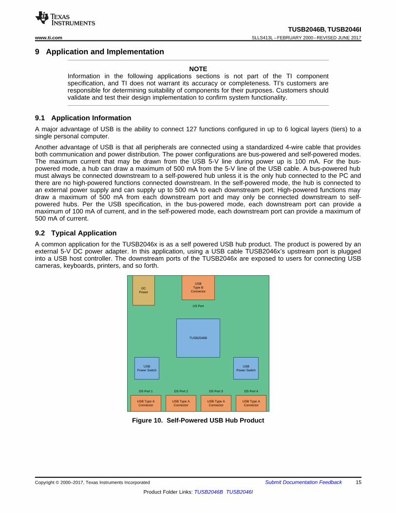
9.2 Typical ApplicationA common application for the TUSB2046x is as a self powered USB hub product. The product is powered by anexternal 5-V DC power adapter. In this application, using a USB cable TUSB2046x’s upstream port is pluggedinto a USB host controller. The downstream ports of the TUSB2046x are exposed to users for connecting USBcameras, keyboards, printers, and so forth.
Figure 10. Self-Powered USB Hub Product
Ω
Ω
1.5 kΩ
Ω
Ω
Ω
Ω
NOTES: A.
B.
C. LDO is a 5-V-to-3.3-V voltage regulatorD. All USB DP, DM signal pairs require series resistors of approximately 27
TPS2044, TPS2042, and SN75240 are Texas Instruments devices. Two TPS2042 devices can be substituted for the TPS2044.The outputs of the TPS204n are open drain. A 10-k pullup is recommended.
120 µF per hub is the minimum required per the USB specification. However, TI recommends a 100-µF, low ESR,tantalum capacitor per port for immunity to voltage droop.
OCn Ω
Ω to ensure proper termination. An optional filtercapacitor of about 22 pF is recommended for EMI suppression. This capacitor, if used, must be placed between the hubterminal and the series resistor, as per section 7.1.6 of the USB specification.
SN75240A
TPS2044A
SN75240A
3.3 V LDOC
D
100 µFB
100 µFB
100 µFB
100 µFB
SN75240A
16
TUSB2046B, TUSB2046ISLLS413L –FEBRUARY 2000–REVISED JUNE 2017 www.ti.com
Product Folder Links: TUSB2046B TUSB2046I
Submit Documentation Feedback Copyright © 2000–2017, Texas Instruments Incorporated
Typical Application (continued)9.2.1 Design RequirementsFor this design example, use the parameters listed in Table 2.
Table 2. Design ParametersDESIGN PARAMETERS VALUE
VCC Supply 3.3-V
Downstream Ports 4
Power Management Individual-Port
Clock Source 6-MHz Crystal
External EEPROM No
Power Source Mode Self-Powered
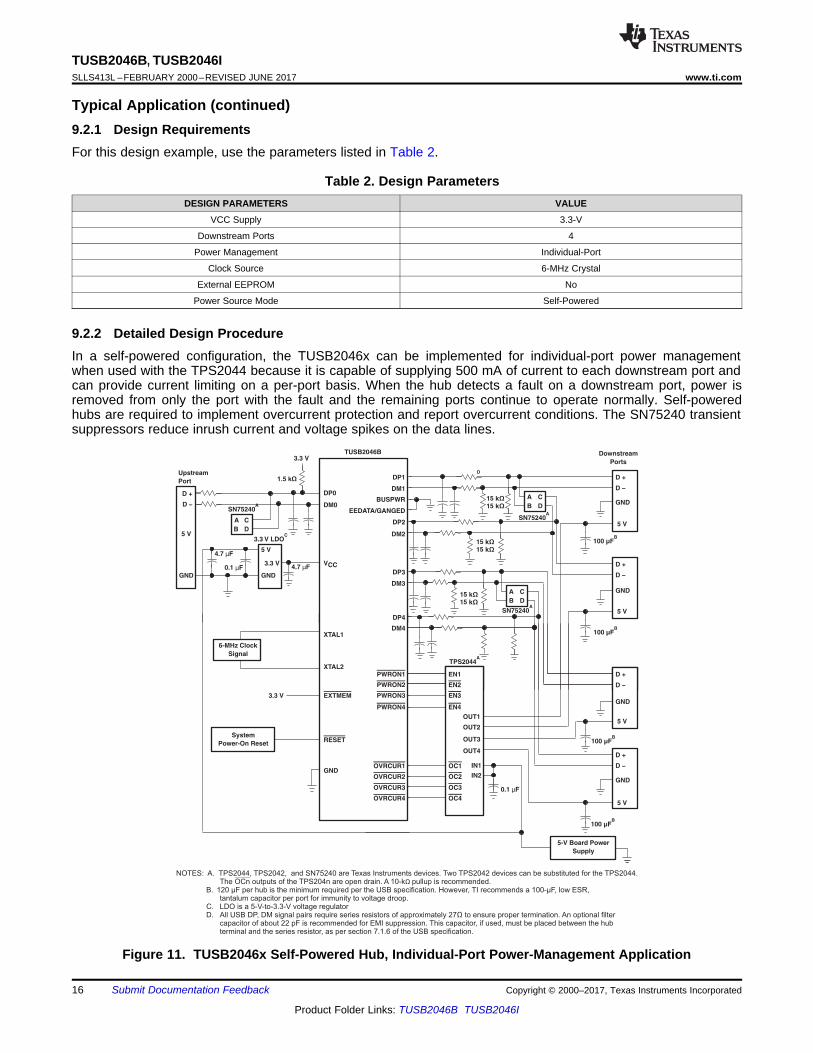
9.2.2 Detailed Design ProcedureIn a self-powered configuration, the TUSB2046x can be implemented for individual-port power managementwhen used with the TPS2044 because it is capable of supplying 500 mA of current to each downstream port andcan provide current limiting on a per-port basis. When the hub detects a fault on a downstream port, power isremoved from only the port with the fault and the remaining ports continue to operate normally. Self-poweredhubs are required to implement overcurrent protection and report overcurrent conditions. The SN75240 transientsuppressors reduce inrush current and voltage spikes on the data lines.
Figure 11. TUSB2046x Self-Powered Hub, Individual-Port Power-Management Application

17
TUSB2046B, TUSB2046Iwww.ti.com SLLS413L –FEBRUARY 2000–REVISED JUNE 2017
Product Folder Links: TUSB2046B TUSB2046I
Submit Documentation FeedbackCopyright © 2000–2017, Texas Instruments Incorporated
9.2.3 Application Curve
Figure 12. Downstream Port 1
10 Power Supply Recommendations
10.1 TUSB2046x Power SupplyVCC should be implemented as a single power plane.• The VCC pins of the TUSB2046x supply 3.3-V power rail to the I/O of the TUSB2046x. This power rail can be
isolated from all other power rails by a ferrite bead to reduce noise.• All power rails require a 10-μF capacitor or 1-μF capacitors for stability and noise immunity. These bulk
capacitors can be placed anywhere on the power rail. The smaller decoupling capacitors should be placed asclose to the TUSB2046x power pins as possible with an optimal grouping of two of differing values per pin.
10.2 Downstream Port Power• The downstream port power, VBUS, must be supplied by a source capable of supplying 5 V and up to 500
mA per port. Downstream port power switches can be controlled by the TUSB2046x signals. It is alsopossible to leave the downstream port power always enabled.
• A large bulk low-ESR capacitor of 22 μF or larger is required on each downstream port’s VBUS to limit in-rushcurrent.
• The ferrite beads on the VBUS pins of the downstream USB port connections are recommended for bothESD and EMI reasons. A 0.1-μF capacitor on the USB connector side of the ferrite provides a low impedancepath to ground for fast rise time ESD current that might have coupled onto the VBUS trace from the cable.

18
TUSB2046B, TUSB2046ISLLS413L –FEBRUARY 2000–REVISED JUNE 2017 www.ti.com
Product Folder Links: TUSB2046B TUSB2046I
Submit Documentation Feedback Copyright © 2000–2017, Texas Instruments Incorporated
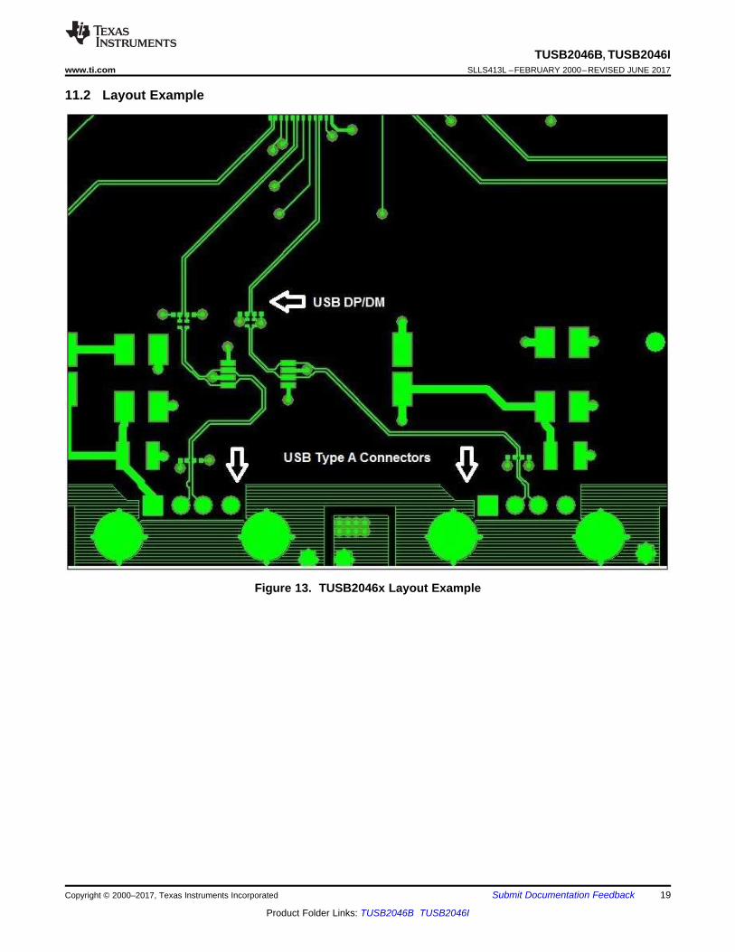
11 Layout
11.1 Layout Guidelines
11.1.1 Placement1. A 0.1-μF should be placed as close as possible on VCC power pin.2. The ESD and EMI protection devices (if used) should also be placed as possible to the USB connector.3. If a crystal is used, it must be placed as close as possible to the TUSB2046x’s XTAL1 and XTAL2 pins.4. Place voltage regulators as far away as possible from the TUSB2046x, the crystal, and the differential pairs.5. In general, the large bulk capacitors associated with the power rail should be placed as close as possible to
the voltage regulators.
11.1.2 Differential Pairs1. Must be designed with a differential impedance of 90Ω ±10%.2. Route all differential pairs on the same layer adjacent to a solid ground plane.3. Do not route differential pairs over any plane split.4. Adding test points will cause impedance discontinuity and will therefore negative impact signal performance.
If test points are used, they should be placed in series and symmetrically. They must not be placed in amanner that causes stub on the differential pair.
5. Avoid 90-degree turns in trace. The use of bends in differential traces should be kept to a minimum. Whenbends are used, the number of left and right bends should be as equal as possible and the angle of the bendshould be ≥ 135 degrees. This will minimize any length mismatch causes by the bends and thereforeminimize the impact bends have on EMI.
6. Minimize the trace lengths of the differential pair traces. The maximum recommended trace length for USB2.0 differential pair signals is 8 inches. Longer trace lengths require very careful routing to assure propersignal integrity.
7. Match the etch lengths of the differential pair traces. The USB 2.0 differential pairs should not exceed 50 milsrelative trace length difference.
8. Minimize the use of vias in the differential pair paths as much as possible. If this is not practical, make surethat the same via type and placement are used for both signals in a pair. Any vias used should be placed asclose as possible to the TUSB2046x device.
9. Do not place power fuses across the differential pair traces.
11.1.3 GroundTI recommends using only one board ground plane in the design. This provides the best image plane for signaltraces running above the plane. The thermal pad of the TUSB2046x and any of the voltage regulators should beconnected to this plane with vias. An earth or chassis ground is implemented only near the USB port connectorson a different plane for EMI and ESD purposes.
19
TUSB2046B, TUSB2046Iwww.ti.com SLLS413L –FEBRUARY 2000–REVISED JUNE 2017
Product Folder Links: TUSB2046B TUSB2046I
Submit Documentation FeedbackCopyright © 2000–2017, Texas Instruments Incorporated
11.2 Layout Example
Figure 13. TUSB2046x Layout Example
20
TUSB2046B, TUSB2046ISLLS413L –FEBRUARY 2000–REVISED JUNE 2017 www.ti.com
Product Folder Links: TUSB2046B TUSB2046I
Submit Documentation Feedback Copyright © 2000–2017, Texas Instruments Incorporated
12 Device and Documentation Support
12.1 Related LinksThe table below lists quick access links. Categories include technical documents, support and communityresources, tools and software, and quick access to order now.
Table 3. Related Links
PARTS PRODUCT FOLDER ORDER NOW TECHNICALDOCUMENTS
TOOLS &SOFTWARE
SUPPORT &COMMUNITY
TUSB2046B Click here Click here Click here Click here Click hereTUSB2046BI Click here Click here Click here Click here Click hereTUSB2046I Click here Click here Click here Click here Click here
12.2 Community ResourcesThe following links connect to TI community resources. Linked contents are provided "AS IS" by the respectivecontributors. They do not constitute TI specifications and do not necessarily reflect TI's views; see TI's Terms ofUse.
TI E2E™ Online Community TI's Engineer-to-Engineer (E2E) Community. Created to foster collaborationamong engineers. At e2e.ti.com, you can ask questions, share knowledge, explore ideas and helpsolve problems with fellow engineers.
Design Support TI's Design Support Quickly find helpful E2E forums along with design support tools andcontact information for technical support.
12.3 TrademarksE2E is a trademark of Texas Instruments.All other trademarks are the property of their respective owners.
12.4 Electrostatic Discharge CautionThese devices have limited built-in ESD protection. The leads should be shorted together or the device placed in conductive foamduring storage or handling to prevent electrostatic damage to the MOS gates.
12.5 GlossarySLYZ022 — TI Glossary.
This glossary lists and explains terms, acronyms, and definitions.
13 Mechanical, Packaging, and Orderable InformationThe following pages include mechanical, packaging, and orderable information. This information is the mostcurrent data available for the designated devices. This data is subject to change without notice and revision ofthis document. For browser-based versions of this data sheet, refer to the left-hand navigation.

PACKAGE OPTION ADDENDUM
www.ti.com 7-May-2018
Addendum-Page 1
PACKAGING INFORMATION
Orderable Device Status(1)
Package Type PackageDrawing
Pins PackageQty
Eco Plan(2)
Lead/Ball Finish(6)
MSL Peak Temp(3)
Op Temp (°C) Device Marking(4/5)
Samples
TUSB2046BIRHBR ACTIVE VQFN RHB 32 3000 Green (RoHS& no Sb/Br)
CU NIPDAU Level-2-260C-1 YEAR -40 to 85 TUSB2046BI
TUSB2046BIRHBRG4 ACTIVE VQFN RHB 32 3000 Green (RoHS& no Sb/Br)
CU NIPDAU Level-2-260C-1 YEAR -40 to 85 TUSB2046BI
TUSB2046BIRHBT ACTIVE VQFN RHB 32 250 Green (RoHS& no Sb/Br)
CU NIPDAU Level-2-260C-1 YEAR -40 to 85 TUSB2046BI
TUSB2046BIRHBTG4 ACTIVE VQFN RHB 32 250 Green (RoHS& no Sb/Br)
CU NIPDAU Level-2-260C-1 YEAR -40 to 85 TUSB2046BI
TUSB2046BVF ACTIVE LQFP VF 32 250 Green (RoHS& no Sb/Br)
CU NIPDAU Level-3-260C-168 HR 0 to 70 TUSB2046B
TUSB2046BVFG4 ACTIVE LQFP VF 32 250 Green (RoHS& no Sb/Br)
CU NIPDAU Level-3-260C-168 HR 0 to 70 TUSB2046B
TUSB2046BVFR ACTIVE LQFP VF 32 1000 Green (RoHS& no Sb/Br)
CU NIPDAU Level-3-260C-168 HR 0 to 70 TUSB2046B
TUSB2046BVFRG4 ACTIVE LQFP VF 32 1000 Green (RoHS& no Sb/Br)
CU NIPDAU Level-3-260C-168 HR 0 to 70 TUSB2046B
TUSB2046IBVF ACTIVE LQFP VF 32 250 Green (RoHS& no Sb/Br)
CU NIPDAU Level-3-260C-168 HR -40 to 85 TUSB2046I
TUSB2046IBVFR ACTIVE LQFP VF 32 1000 Green (RoHS& no Sb/Br)
CU NIPDAU Level-3-260C-168 HR -40 to 85 TUSB2046I
(1) The marketing status values are defined as follows:ACTIVE: Product device recommended for new designs.LIFEBUY: TI has announced that the device will be discontinued, and a lifetime-buy period is in effect.NRND: Not recommended for new designs. Device is in production to support existing customers, but TI does not recommend using this part in a new design.PREVIEW: Device has been announced but is not in production. Samples may or may not be available.OBSOLETE: TI has discontinued the production of the device.
(2) RoHS: TI defines "RoHS" to mean semiconductor products that are compliant with the current EU RoHS requirements for all 10 RoHS substances, including the requirement that RoHS substancedo not exceed 0.1% by weight in homogeneous materials. Where designed to be soldered at high temperatures, "RoHS" products are suitable for use in specified lead-free processes. TI mayreference these types of products as "Pb-Free".RoHS Exempt: TI defines "RoHS Exempt" to mean products that contain lead but are compliant with EU RoHS pursuant to a specific EU RoHS exemption.Green: TI defines "Green" to mean the content of Chlorine (Cl) and Bromine (Br) based flame retardants meet JS709B low halogen requirements of <=1000ppm threshold. Antimony trioxide basedflame retardants must also meet the <=1000ppm threshold requirement.
(3) MSL, Peak Temp. - The Moisture Sensitivity Level rating according to the JEDEC industry standard classifications, and peak solder temperature.
PACKAGE OPTION ADDENDUM
www.ti.com 7-May-2018
Addendum-Page 2
(4) There may be additional marking, which relates to the logo, the lot trace code information, or the environmental category on the device.
(5) Multiple Device Markings will be inside parentheses. Only one Device Marking contained in parentheses and separated by a "~" will appear on a device. If a line is indented then it is a continuationof the previous line and the two combined represent the entire Device Marking for that device.
(6) Lead/Ball Finish - Orderable Devices may have multiple material finish options. Finish options are separated by a vertical ruled line. Lead/Ball Finish values may wrap to two lines if the finishvalue exceeds the maximum column width.
Important Information and Disclaimer:The information provided on this page represents TI's knowledge and belief as of the date that it is provided. TI bases its knowledge and belief on informationprovided by third parties, and makes no representation or warranty as to the accuracy of such information. Efforts are underway to better integrate information from third parties. TI has taken andcontinues to take reasonable steps to provide representative and accurate information but may not have conducted destructive testing or chemical analysis on incoming materials and chemicals.TI and TI suppliers consider certain information to be proprietary, and thus CAS numbers and other limited information may not be available for release.
In no event shall TI's liability arising out of such information exceed the total purchase price of the TI part(s) at issue in this document sold by TI to Customer on an annual basis.

TAPE AND REEL INFORMATION
*All dimensions are nominal
Device PackageType
PackageDrawing
Pins SPQ ReelDiameter
(mm)
ReelWidth
W1 (mm)
A0(mm)
B0(mm)
K0(mm)
P1(mm)
W(mm)
Pin1Quadrant
TUSB2046BIRHBR VQFN RHB 32 3000 330.0 12.4 5.3 5.3 1.5 8.0 12.0 Q2
TUSB2046BIRHBT VQFN RHB 32 250 180.0 12.4 5.3 5.3 1.5 8.0 12.0 Q2
TUSB2046BVFR LQFP VF 32 1000 330.0 16.4 9.6 9.6 1.9 12.0 16.0 Q2
TUSB2046IBVFR LQFP VF 32 1000 330.0 16.4 9.6 9.6 1.9 12.0 16.0 Q2
PACKAGE MATERIALS INFORMATION
www.ti.com 30-Jun-2017
Pack Materials-Page 1
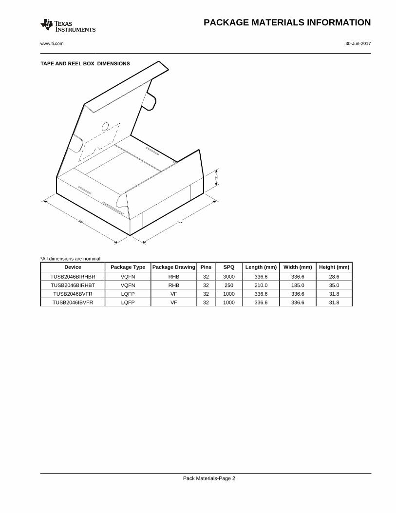
*All dimensions are nominal
Device Package Type Package Drawing Pins SPQ Length (mm) Width (mm) Height (mm)
TUSB2046BIRHBR VQFN RHB 32 3000 336.6 336.6 28.6
TUSB2046BIRHBT VQFN RHB 32 250 210.0 185.0 35.0
TUSB2046BVFR LQFP VF 32 1000 336.6 336.6 31.8
TUSB2046IBVFR LQFP VF 32 1000 336.6 336.6 31.8
PACKAGE MATERIALS INFORMATION
www.ti.com 30-Jun-2017
Pack Materials-Page 2

MECHANICAL DATA
MTQF002B – JANUARY 1995 – REVISED MAY 2000
1POST OFFICE BOX 655303 • DALLAS, TEXAS 75265
VF (S-PQFP-G32) PLASTIC QUAD FLATPACK
4040172/D 04/00
Gage Plane
Seating Plane
1,60 MAX
1,451,35
8,809,20
SQ
0,05 MIN
0,450,75
0,25
0,13 NOM
5,60 TYP
1
32
7,206,80
24
25
SQ
8
9
17
16
0,250,45
0,10
0°–7°
M0,200,80
NOTES: A. All linear dimensions are in millimeters.B. This drawing is subject to change without notice.
IMPORTANT NOTICE
Texas Instruments Incorporated (TI) reserves the right to make corrections, enhancements, improvements and other changes to itssemiconductor products and services per JESD46, latest issue, and to discontinue any product or service per JESD48, latest issue. Buyersshould obtain the latest relevant information before placing orders and should verify that such information is current and complete.TI’s published terms of sale for semiconductor products (http://www.ti.com/sc/docs/stdterms.htm) apply to the sale of packaged integratedcircuit products that TI has qualified and released to market. Additional terms may apply to the use or sale of other types of TI products andservices.Reproduction of significant portions of TI information in TI data sheets is permissible only if reproduction is without alteration and isaccompanied by all associated warranties, conditions, limitations, and notices. TI is not responsible or liable for such reproduceddocumentation. Information of third parties may be subject to additional restrictions. Resale of TI products or services with statementsdifferent from or beyond the parameters stated by TI for that product or service voids all express and any implied warranties for theassociated TI product or service and is an unfair and deceptive business practice. TI is not responsible or liable for any such statements.Buyers and others who are developing systems that incorporate TI products (collectively, “Designers”) understand and agree that Designersremain responsible for using their independent analysis, evaluation and judgment in designing their applications and that Designers havefull and exclusive responsibility to assure the safety of Designers' applications and compliance of their applications (and of all TI productsused in or for Designers’ applications) with all applicable regulations, laws and other applicable requirements. Designer represents that, withrespect to their applications, Designer has all the necessary expertise to create and implement safeguards that (1) anticipate dangerousconsequences of failures, (2) monitor failures and their consequences, and (3) lessen the likelihood of failures that might cause harm andtake appropriate actions. Designer agrees that prior to using or distributing any applications that include TI products, Designer willthoroughly test such applications and the functionality of such TI products as used in such applications.TI’s provision of technical, application or other design advice, quality characterization, reliability data or other services or information,including, but not limited to, reference designs and materials relating to evaluation modules, (collectively, “TI Resources”) are intended toassist designers who are developing applications that incorporate TI products; by downloading, accessing or using TI Resources in anyway, Designer (individually or, if Designer is acting on behalf of a company, Designer’s company) agrees to use any particular TI Resourcesolely for this purpose and subject to the terms of this Notice.TI’s provision of TI Resources does not expand or otherwise alter TI’s applicable published warranties or warranty disclaimers for TIproducts, and no additional obligations or liabilities arise from TI providing such TI Resources. TI reserves the right to make corrections,enhancements, improvements and other changes to its TI Resources. TI has not conducted any testing other than that specificallydescribed in the published documentation for a particular TI Resource.Designer is authorized to use, copy and modify any individual TI Resource only in connection with the development of applications thatinclude the TI product(s) identified in such TI Resource. NO OTHER LICENSE, EXPRESS OR IMPLIED, BY ESTOPPEL OR OTHERWISETO ANY OTHER TI INTELLECTUAL PROPERTY RIGHT, AND NO LICENSE TO ANY TECHNOLOGY OR INTELLECTUAL PROPERTYRIGHT OF TI OR ANY THIRD PARTY IS GRANTED HEREIN, including but not limited to any patent right, copyright, mask work right, orother intellectual property right relating to any combination, machine, or process in which TI products or services are used. Informationregarding or referencing third-party products or services does not constitute a license to use such products or services, or a warranty orendorsement thereof. Use of TI Resources may require a license from a third party under the patents or other intellectual property of thethird party, or a license from TI under the patents or other intellectual property of TI.TI RESOURCES ARE PROVIDED “AS IS” AND WITH ALL FAULTS. TI DISCLAIMS ALL OTHER WARRANTIES ORREPRESENTATIONS, EXPRESS OR IMPLIED, REGARDING RESOURCES OR USE THEREOF, INCLUDING BUT NOT LIMITED TOACCURACY OR COMPLETENESS, TITLE, ANY EPIDEMIC FAILURE WARRANTY AND ANY IMPLIED WARRANTIES OFMERCHANTABILITY, FITNESS FOR A PARTICULAR PURPOSE, AND NON-INFRINGEMENT OF ANY THIRD PARTY INTELLECTUALPROPERTY RIGHTS. TI SHALL NOT BE LIABLE FOR AND SHALL NOT DEFEND OR INDEMNIFY DESIGNER AGAINST ANY CLAIM,INCLUDING BUT NOT LIMITED TO ANY INFRINGEMENT CLAIM THAT RELATES TO OR IS BASED ON ANY COMBINATION OFPRODUCTS EVEN IF DESCRIBED IN TI RESOURCES OR OTHERWISE. IN NO EVENT SHALL TI BE LIABLE FOR ANY ACTUAL,DIRECT, SPECIAL, COLLATERAL, INDIRECT, PUNITIVE, INCIDENTAL, CONSEQUENTIAL OR EXEMPLARY DAMAGES INCONNECTION WITH OR ARISING OUT OF TI RESOURCES OR USE THEREOF, AND REGARDLESS OF WHETHER TI HAS BEENADVISED OF THE POSSIBILITY OF SUCH DAMAGES.Unless TI has explicitly designated an individual product as meeting the requirements of a particular industry standard (e.g., ISO/TS 16949and ISO 26262), TI is not responsible for any failure to meet such industry standard requirements.Where TI specifically promotes products as facilitating functional safety or as compliant with industry functional safety standards, suchproducts are intended to help enable customers to design and create their own applications that meet applicable functional safety standardsand requirements. Using products in an application does not by itself establish any safety features in the application. Designers mustensure compliance with safety-related requirements and standards applicable to their applications. Designer may not use any TI products inlife-critical medical equipment unless authorized officers of the parties have executed a special contract specifically governing such use.Life-critical medical equipment is medical equipment where failure of such equipment would cause serious bodily injury or death (e.g., lifesupport, pacemakers, defibrillators, heart pumps, neurostimulators, and implantables). Such equipment includes, without limitation, allmedical devices identified by the U.S. Food and Drug Administration as Class III devices and equivalent classifications outside the U.S.TI may expressly designate certain products as completing a particular qualification (e.g., Q100, Military Grade, or Enhanced Product).Designers agree that it has the necessary expertise to select the product with the appropriate qualification designation for their applicationsand that proper product selection is at Designers’ own risk. Designers are solely responsible for compliance with all legal and regulatoryrequirements in connection with such selection.Designer will fully indemnify TI and its representatives against any damages, costs, losses, and/or liabilities arising out of Designer’s non-compliance with the terms and provisions of this Notice.
Mailing Address: Texas Instruments, Post Office Box 655303, Dallas, Texas 75265Copyright © 2018, Texas Instruments Incorporated