Special Mission Audio Controller System with MultiTalker ...
Upload
vuongtuyenCategory
view
229download
0
1
Techwell, Inc. www.techwellinc.com Datasheet Rev. 1.2
Oct, 10, 2006
TW2835
4 Channel Video and Audio Controller
For Security Applications
Preliminary Data Sheet from Techwell, Inc. Information may change without notice
Disclaimer
This document provides technical information for the user. Techwell Inc. reserves the right to modify the information in this document as necessary. The customer should make sure that they have the most recent data sheet version. Techwell Inc. holds no responsibility for any errors that may appear in this document. Customers should take appropriate action to ensure their use of the products does not infringe upon any patents. Techwell Inc. respects valid patent rights of third parties and does not infringe upon or assist others to infringe upon such rights.

2
Techwell, Inc. www.techwellinc.com Datasheet Rev. 1.2
PreliminaryTW2835 Video and Audio Controller
Oct, 10, 2006
Table of Contents
Introduction........................................................................................................................................... 5
Features ............................................................................................................................................. 5
Applications ...................................................................................................................................... 6
Block Diagram .................................................................................................................................. 7
Pin Description ................................................................................................................................. 8
Pin Diagram.................................................................................................................................... 15
Functional Description ....................................................................................................................... 17
Video Input ..................................................................................................................................... 17
Analog Video Input ...................................................................................................................... 18
Anti-aliasing Filter ................................................................................................................... 19
Analog-to-Digital Converter .................................................................................................... 19
Sync Processing........................................................................................................................ 20
Color Decoding ........................................................................................................................ 21
Luminance Processing.............................................................................................................. 23
Chrominance Processing .......................................................................................................... 24
Realtime Record Mode............................................................................................................. 25
Digital Video Input....................................................................................................................... 26
Digital Video Input Format ...................................................................................................... 26
Channel ID Decoder ................................................................................................................. 27
Cropping and Scaling Function.................................................................................................... 29
Cropping Function for Live...................................................................................................... 29
Scaling Function for Live......................................................................................................... 30
Cropping and Scaling Function for Playback........................................................................... 34
Motion Detection ............................................................................................................................ 36
Mask and Detection Region Selection ......................................................................................... 37
Sensitivity Control ....................................................................................................................... 38
Level Sensitivity....................................................................................................................... 38
Spatial Sensitivity..................................................................................................................... 38
Temporal Sensitivity ................................................................................................................ 38
Velocity Control ........................................................................................................................... 39
Blind Detection ............................................................................................................................ 41
Night Detection ............................................................................................................................ 41
Video Control ................................................................................................................................. 42
Channel Input Selection ............................................................................................................... 43
Channel Operation Mode ............................................................................................................. 44

3
Techwell, Inc. www.techwellinc.com Datasheet Rev. 1.2
PreliminaryTW2835 Video and Audio Controller
Oct, 10, 2006
Live Mode ................................................................................................................................ 44
Strobe Mode ............................................................................................................................. 45
Switch Mode............................................................................................................................. 47
Channel Attribute ......................................................................................................................... 51
Background Control ................................................................................................................. 51
Boundary Control ..................................................................................................................... 51
Blank Control ........................................................................................................................... 51
Freeze Control .......................................................................................................................... 51
Last Image Captured ................................................................................................................ 52
Horizontal / Vertical Mirroring ................................................................................................ 52
Field to Frame Conversion ....................................................................................................... 52
Display Path Control .................................................................................................................... 53
Save and Recall Function ......................................................................................................... 53
Image Enhancement ................................................................................................................. 54
Zoom Function ......................................................................................................................... 54
Picture Size and Popup Control................................................................................................ 55
Full Triplex Function................................................................................................................ 56
Playback Path Control .................................................................................................................. 57
Frame Record Mode ................................................................................................................. 59
DVR Normal Record Mode...................................................................................................... 61
DVR Frame Record Mode........................................................................................................ 62
Record Path Control ..................................................................................................................... 64
Normal Record Mode ............................................................................................................... 65
Frame Record Mode ................................................................................................................. 66
DVR Normal Record Mode...................................................................................................... 67
DVR Frame Record Mode........................................................................................................ 68
Noise Reduction ....................................................................................................................... 69
Channel ID Encoder ..................................................................................................................... 70
Channel ID Information ........................................................................................................... 70
Analog Type Channel ID in VBI.............................................................................................. 73
Digital Type Channel ID in VBI .............................................................................................. 74
Digital Type Channel ID in Channel Boundary ....................................................................... 75
Chip-to-Chip Cascade Operation ................................................................................................. 76
Channel Priority Control .......................................................................................................... 76
120 CIF/Sec Record Mode ....................................................................................................... 78
240 CIF/Sec Record Mode ....................................................................................................... 79
480 CIF/Sec Record Mode ....................................................................................................... 80
Infinite Cascade Mode for Display Path .................................................................................. 81
OSD (On Screen Display) Control ............................................................................................... 82
2 Dimensional Arrayed Box..................................................................................................... 83
Bitmap Overlay ........................................................................................................................ 85

4
Techwell, Inc. www.techwellinc.com Datasheet Rev. 1.2
PreliminaryTW2835 Video and Audio Controller
Oct, 10, 2006
Single Box ................................................................................................................................ 89
Mouse Pointer........................................................................................................................... 89
Video Output .................................................................................................................................. 90
Timing Interface and Control ....................................................................................................... 91
Analog Video Output ................................................................................................................... 93
Output Standard Selection........................................................................................................ 93
Luminance Filter ...................................................................................................................... 94
Chrominance Filter................................................................................................................... 94
Digital-to-Analog Converter .................................................................................................... 95
Digital Video Output .................................................................................................................... 96
Single Output Mode ................................................................................................................. 97
Dual Output Mode.................................................................................................................... 98
Audio CODEC ................................................................................................................................ 99
Multi-Chip Operation ................................................................................................................. 100
Serial Audio Interface ................................................................................................................ 102
Analog Audio Output ................................................................................................................. 105
Host Interface.................................................................................................................................... 106
Serial Interface ............................................................................................................................. 107
Parallel Interface.......................................................................................................................... 109
Interrupt Interface ....................................................................................................................... 111
MPP Pin Interface........................................................................................................................ 112
Control Register ........................................................................................................................... 113
Register Map .............................................................................................................................. 113
Recommended Value.................................................................................................................. 122
Register Description................................................................................................................... 127
Parametric Information .................................................................................................................... 247
DC Electrical Parameters ............................................................................................................ 247
AC Electrical Parameters ............................................................................................................ 249
Application Schematic ...................................................................................................................... 253
Package Dimension........................................................................................................................... 254
Revision History ................................................................................................................................ 256
5
Techwell, Inc. www.techwellinc.com Datasheet Rev. 1.2
PreliminaryTW2835 Video and Audio Controller
Oct, 10, 2006
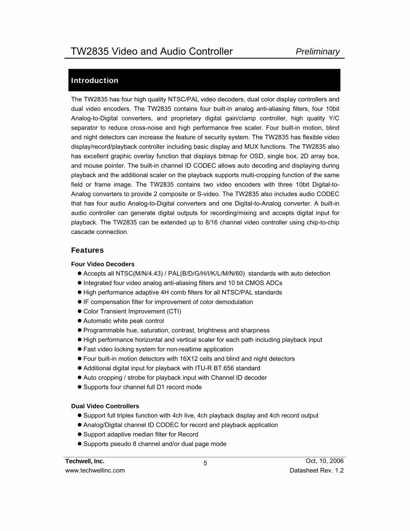
Introduction
The TW2835 has four high quality NTSC/PAL video decoders, dual color display controllers and dual video encoders. The TW2835 contains four built-in analog anti-aliasing filters, four 10bit Analog-to-Digital converters, and proprietary digital gain/clamp controller, high quality Y/C separator to reduce cross-noise and high performance free scaler. Four built-in motion, blind and night detectors can increase the feature of security system. The TW2835 has flexible video display/record/playback controller including basic display and MUX functions. The TW2835 also has excellent graphic overlay function that displays bitmap for OSD, single box, 2D array box, and mouse pointer. The built-in channel ID CODEC allows auto decoding and displaying during playback and the additional scaler on the playback supports multi-cropping function of the same field or frame image. The TW2835 contains two video encoders with three 10bit Digital-to-Analog converters to provide 2 composite or S-video. The TW2835 also includes audio CODEC that has four audio Analog-to-Digital converters and one Digital-to-Analog converter. A built-in audio controller can generate digital outputs for recording/mixing and accepts digital input for playback. The TW2835 can be extended up to 8/16 channel video controller using chip-to-chip cascade connection.
Features
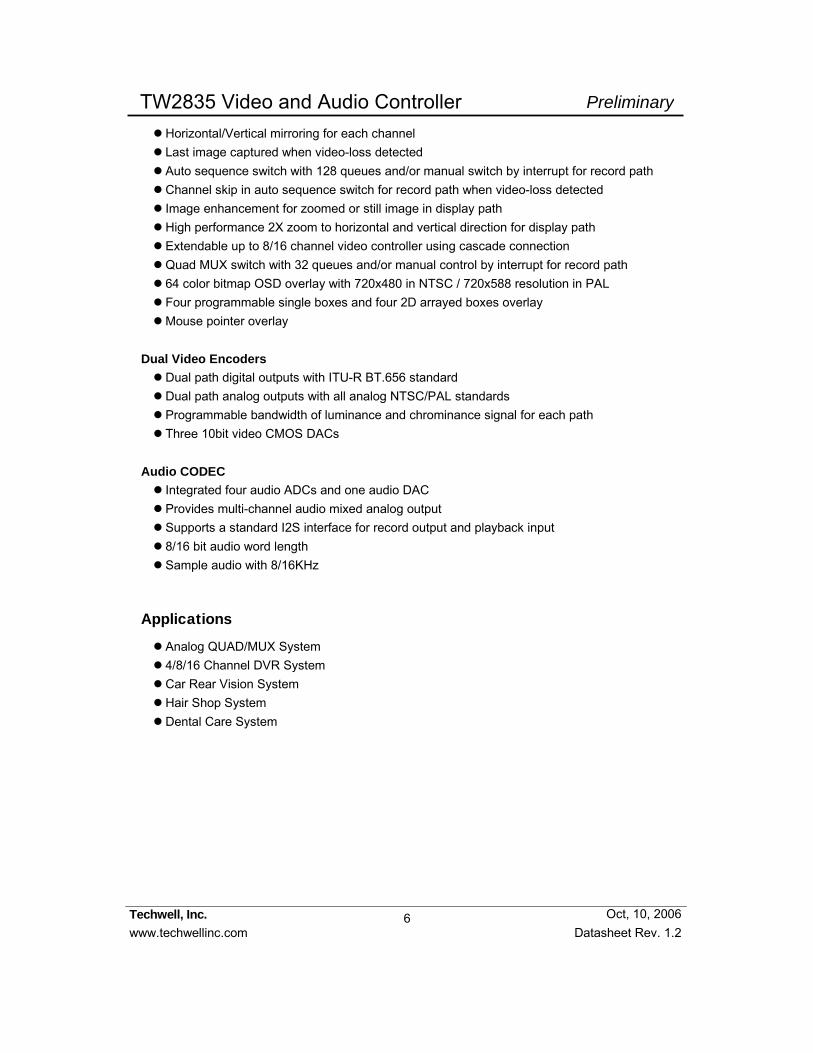
Four Video Decoders Accepts all NTSC(M/N/4.43) / PAL(B/D/G/H/I/K/L/M/N/60) standards with auto detection Integrated four video analog anti-aliasing filters and 10 bit CMOS ADCs High performance adaptive 4H comb filters for all NTSC/PAL standards IF compensation filter for improvement of color demodulation Color Transient Improvement (CTI) Automatic white peak control Programmable hue, saturation, contrast, brightness and sharpness High performance horizontal and vertical scaler for each path including playback input Fast video locking system for non-realtime application Four built-in motion detectors with 16X12 cells and blind and night detectors Additional digital input for playback with ITU-R BT.656 standard Auto cropping / strobe for playback input with Channel ID decoder Supports four channel full D1 record mode
Dual Video Controllers Support full triplex function with 4ch live, 4ch playback display and 4ch record output Analog/Digital channel ID CODEC for record and playback application Support adaptive median filter for Record Supports pseudo 8 channel and/or dual page mode
6
Techwell, Inc. www.techwellinc.com Datasheet Rev. 1.2
PreliminaryTW2835 Video and Audio Controller
Oct, 10, 2006
Horizontal/Vertical mirroring for each channel Last image captured when video-loss detected Auto sequence switch with 128 queues and/or manual switch by interrupt for record path Channel skip in auto sequence switch for record path when video-loss detected Image enhancement for zoomed or still image in display path High performance 2X zoom to horizontal and vertical direction for display path Extendable up to 8/16 channel video controller using cascade connection Quad MUX switch with 32 queues and/or manual control by interrupt for record path 64 color bitmap OSD overlay with 720x480 in NTSC / 720x588 resolution in PAL Four programmable single boxes and four 2D arrayed boxes overlay Mouse pointer overlay
Dual Video Encoders Dual path digital outputs with ITU-R BT.656 standard Dual path analog outputs with all analog NTSC/PAL standards Programmable bandwidth of luminance and chrominance signal for each path Three 10bit video CMOS DACs
Audio CODEC Integrated four audio ADCs and one audio DAC Provides multi-channel audio mixed analog output Supports a standard I2S interface for record output and playback input 8/16 bit audio word length Sample audio with 8/16KHz
Applications
Analog QUAD/MUX System 4/8/16 Channel DVR System Car Rear Vision System Hair Shop System Dental Care System
7
Techwell, Inc. www.techwellinc.com Datasheet Rev. 1.2
PreliminaryTW2835 Video and Audio Controller
Oct, 10, 2006
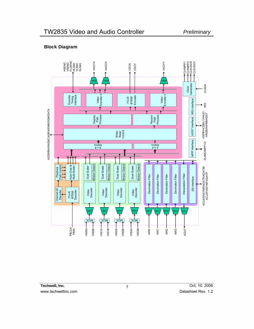
Block Diagram
PBC
LKPB
IN
VD
OY
VIN
0B
VIN
0A
MUX
Mot
ion
Det
ect
ITU
-RB
T656
Dec
oder
VAO
YX
AD
DR
/BA
/RA
SB/C
ASB
/WEN
B/D
QM
/DA
TA
VD
OX
VAO
CX
Clo
ck
Gen
erat
or
CLK
54I
IRQ
IRQ
Inte
rface
HO
ST
Inte
rface
VAO
YY
CLK
VD
OX
CLK
VD
OY
HSP
B/H
CSB
0,1/
HA
LE/
HR
DB
/HW
RB/
HD
AT
HSE
NC
VSEN
CFL
DE
NC
HLI
NK
IV
LIN
KI
DLI
NK
I
ITU
-RB
T656
E
ncod
er
Writ
e/R
ead
Con
trol
Dua
l Sca
ler
Vid
eoD
ecod
erD
ispl
ayP
ath
Pro
cess
Rec
ord
Pat
hP
roce
ss
4 x 4Matrix
8 x 8Matrix
Aut
o-C
rop
&M
ulti-
Sca
ler
DLI
NK
I/MP
P1/2
MP
P In
terfa
ce
Enc
oder
Tim
ing
Inte
rface
Cha
nnel
IDD
ecod
er
CLK
MPP
1C
LKM
PP2
Pla
ybac
kP
ath
Con
trol
DACDACDAC
AO
UT
Vid
eoE
ncod
er II
Vid
eoE
ncod
er II
AIN
3
AIN
2
AIN
1
ADC
Dec
imat
ion
Filte
rA
IN0
VIN
1B
VIN
1A
MUXM
otio
n D
etec
t
Dua
l Sca
ler
Vid
eoD
ecod
er
VIN
2B
VIN
2A
MUX
Mot
ion
Det
ect
Dua
l Sca
ler
Vid
eoD
ecod
er
VIN
3B
VIN
3A
MUX
Mot
ion
Det
ect
Dua
l Sca
ler
Vid
eoD
ecod
er
AC
LKR
/AS
YNR
/AD
ATR
/AD
ATM
/A
CLK
P/A
SYN
P/A
DA
TPADC ADC ADC DAC
Dec
imat
ion
Filte
r
Dec
imat
ion
Filte
r
Dec
imat
ion
Filte
r
Inte
rpol
atio
n Fi
lter
I2S
Inte
rface
ADC ADC ADC ADC
8
Techwell, Inc. www.techwellinc.com Datasheet Rev. 1.2
PreliminaryTW2835 Video and Audio Controller
Oct, 10, 2006
Pin Description
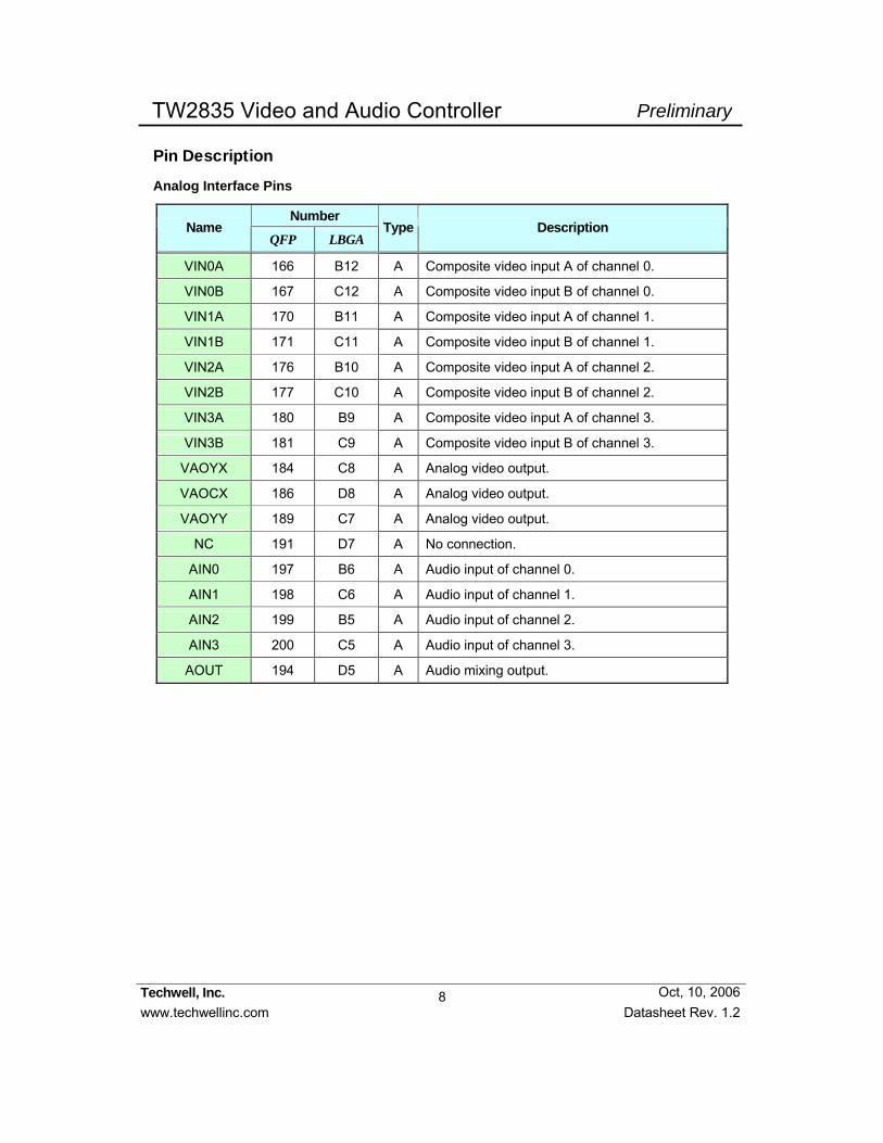
Analog Interface Pins
Number Name
QFP LBGA Type Description
VIN0A 166 B12 A Composite video input A of channel 0.
VIN0B 167 C12 A Composite video input B of channel 0.
VIN1A 170 B11 A Composite video input A of channel 1.
VIN1B 171 C11 A Composite video input B of channel 1.
VIN2A 176 B10 A Composite video input A of channel 2.
VIN2B 177 C10 A Composite video input B of channel 2.
VIN3A 180 B9 A Composite video input A of channel 3.
VIN3B 181 C9 A Composite video input B of channel 3.
VAOYX 184 C8 A Analog video output.
VAOCX 186 D8 A Analog video output.
VAOYY 189 C7 A Analog video output.
NC 191 D7 A No connection.
AIN0 197 B6 A Audio input of channel 0.
AIN1 198 C6 A Audio input of channel 1.
AIN2 199 B5 A Audio input of channel 2.
AIN3 200 C5 A Audio input of channel 3.
AOUT 194 D5 A Audio mixing output.
9
Techwell, Inc. www.techwellinc.com Datasheet Rev. 1.2
PreliminaryTW2835 Video and Audio Controller
Oct, 10, 2006
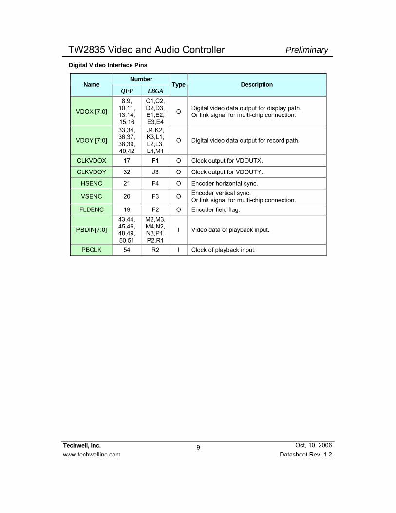
Digital Video Interface Pins
Number Name
QFP LBGA Type Description
VDOX [7:0]
8,9, 10,11, 13,14, 15,16
C1,C2, D2,D3, E1,E2, E3,E4
O Digital video data output for display path. Or link signal for multi-chip connection.
VDOY [7:0]
33,34, 36,37, 38,39, 40,42
J4,K2, K3,L1, L2,L3, L4,M1
O Digital video data output for record path.
CLKVDOX 17 F1 O Clock output for VDOUTX.
CLKVDOY 32 J3 O Clock output for VDOUTY..
HSENC 21 F4 O Encoder horizontal sync.
VSENC 20 F3 O Encoder vertical sync. Or link signal for multi-chip connection.
FLDENC 19 F2 O Encoder field flag.
PBDIN[7:0]
43,44, 45,46, 48,49, 50,51
M2,M3, M4,N2, N3,P1, P2,R1
I Video data of playback input.
PBCLK 54 R2 I Clock of playback input.

10
Techwell, Inc. www.techwellinc.com Datasheet Rev. 1.2
PreliminaryTW2835 Video and Audio Controller
Oct, 10, 2006
Multi-purpose Pins
Number Name
QFP LBGA Type Description
HLINKI 138 F14 I/O Link signal for multi-chip connection.
VLINKI 140 F13 I Link signal for multi-chip connection.
DLINKI[7:0]
149,148, 147,146, 144,143, 142,141
C15,C16,D14,D15,E13,E14,E15,E16
I/O
Link signal for multi-chip connection. Or decoder’s bypassed data output. Or decoder’s timing signal output. Or general purpose input/output.
MPP1[7:0]
204,205, 206,207,
2,3, 4,5
A4,B4, C4,A3, B3,C3, A2,B2
I/O Decoder’s bypassed data output. Or decoder’s timing signal output. Or general purpose input/output.
MPP2[7:0]
152,153, 154,155, 158,159, 160,161
B16,B15,A15,A14,B14,A13,B13,C13
I/O Decoder’s bypassed data output. Or decoder’s timing signal output. Or general purpose input/output.
CLKMPP1 7 B1 O Clock output for MPP1 data.
CLKMPP2 150 C14 O Clock output for MPP2 data.
11
Techwell, Inc. www.techwellinc.com Datasheet Rev. 1.2
PreliminaryTW2835 Video and Audio Controller
Oct, 10, 2006
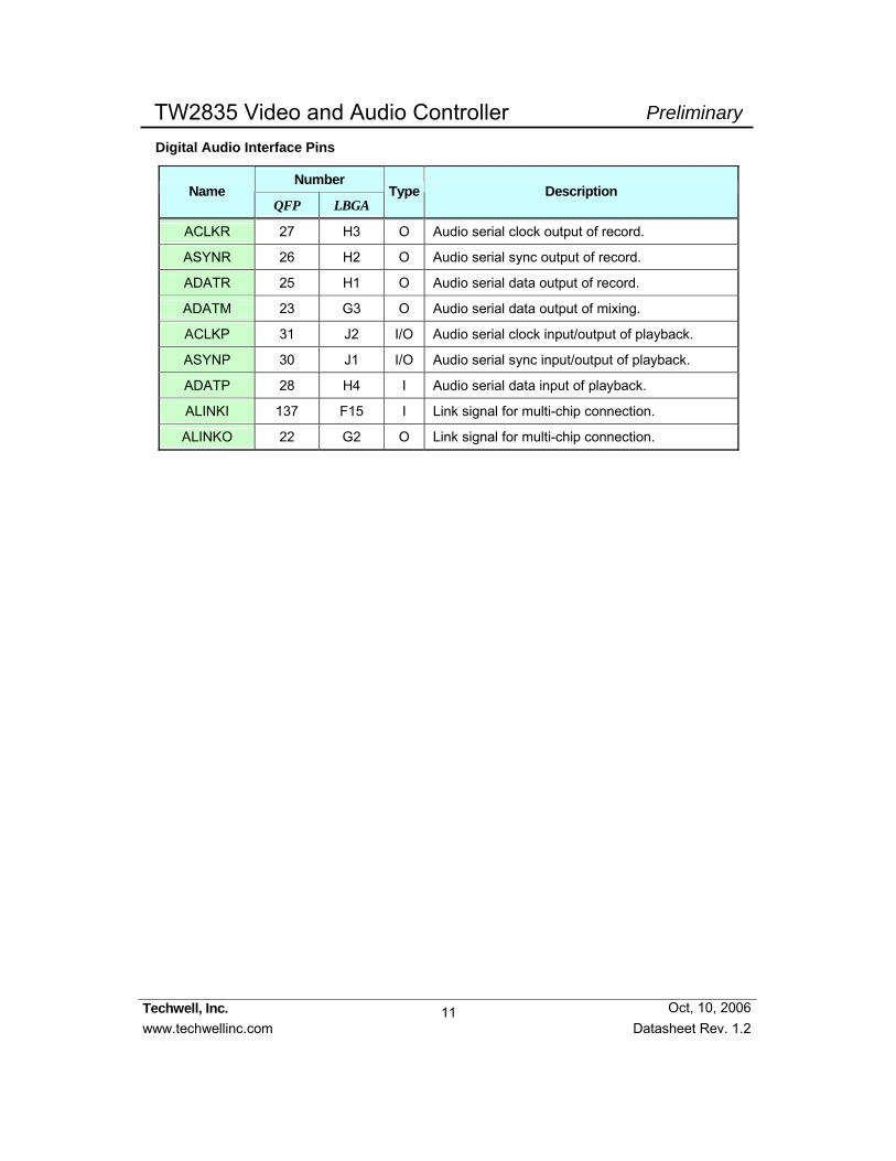
Digital Audio Interface Pins
Number Name
QFP LBGA Type Description
ACLKR 27 H3 O Audio serial clock output of record.
ASYNR 26 H2 O Audio serial sync output of record.
ADATR 25 H1 O Audio serial data output of record.
ADATM 23 G3 O Audio serial data output of mixing.
ACLKP 31 J2 I/O Audio serial clock input/output of playback.
ASYNP 30 J1 I/O Audio serial sync input/output of playback.
ADATP 28 H4 I Audio serial data input of playback.
ALINKI 137 F15 I Link signal for multi-chip connection.
ALINKO 22 G2 O Link signal for multi-chip connection.

12
Techwell, Inc. www.techwellinc.com Datasheet Rev. 1.2
PreliminaryTW2835 Video and Audio Controller
Oct, 10, 2006
Memory Interface Pins
Number Name
QFP LBGA Type Description
DATA[31:0]
76,77, 78,79, 80,82, 83,84, 85,86, 88,89, 90,91, 92,94,
118,119, 120,121, 123,124, 125,126, 127,129, 130,131, 132,134, 135,136
R8,P8, N8,T9, R9,P9,
N9,R10,P10,T11,R11,P11,N11,T12,R12,P12,L15,L14,L13,K15,K14,J16,J15,J14,J13,H16,H15,H14,H13,G15,G14,F16
I/O SDRAM data bus.
ADDR[10:0]
95,96, 97,98,
100,101, 102,103, 106,107,
108
N12,R13,P13,T14,R14,P14,T15,R15,R16,P16,
P15
O SDRAM address bus. ADDR[10] is AP.
BA1 109 N15 O SDRAM bank1 selection.
BA0 111 N14 O SDRAM bank0 selection.
RASB 113 M15 O SDRAM row address selection.
CASB 114 M14 O SDRAM column address selection.
WEB 115 M13 O SDRAM write enable.
DQM 117 L16 O SDRAM write mask.
CLK54MEM 112 M16 O SDRAM clock.
13
Techwell, Inc. www.techwellinc.com Datasheet Rev. 1.2
PreliminaryTW2835 Video and Audio Controller
Oct, 10, 2006
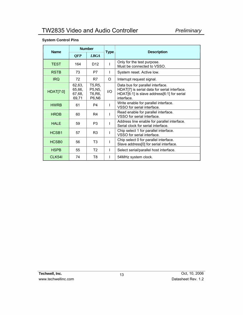
System Control Pins
Number Name
QFP LBGA Type Description
TEST 164 D12 I Only for the test purpose. Must be connected to VSSO.
RSTB 73 P7 I System reset. Active low.
IRQ 72 R7 O Interrupt request signal.
HDAT[7:0]
62,63, 65,66, 67,68, 69,71
T5,R5, P5,N5, T6,R6, P6,N6
I/O
Data bus for parallel interface. HDAT[7] is serial data for serial interface. HDAT[6:1] is slave address[6:1] for serial interface.
HWRB 61 P4 I Write enable for parallel interface. VSSO for serial interface.
HRDB 60 R4 I Read enable for parallel interface. VSSO for serial interface.
HALE 59 P3 I Address line enable for parallel interface. Serial clock for serial interface.
HCSB1 57 R3 I Chip select 1 for parallel interface. VSSO for serial interface.
HCSB0 56 T3 I Chip select 0 for parallel interface. Slave address[0] for serial interface.
HSPB 55 T2 I Select serial/parallel host interface.
CLK54I 74 T8 I 54MHz system clock.
14
Techwell, Inc. www.techwellinc.com Datasheet Rev. 1.2
PreliminaryTW2835 Video and Audio Controller
Oct, 10, 2006
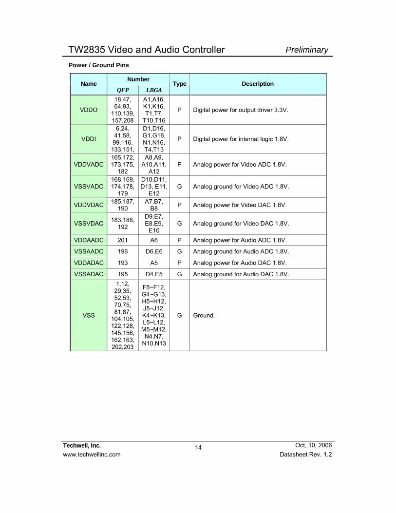
Power / Ground Pins
Number Name
QFP LBGA Type Description
VDDO
18,47, 64,93,
110,139, 157,208
A1,A16, K1,K16, T1,T7,
T10,T16
P Digital power for output driver 3.3V.
VDDI
6,24, 41,58, 99,116, 133,151,
D1,D16, G1,G16, N1,N16, T4,T13
P Digital power for internal logic 1.8V.
VDDVADC 165,172, 173,175,
182
A8,A9, A10,A11,
A12 P Analog power for Video ADC 1.8V.
VSSVADC 168,169, 174,178,
179
D10,D11,D13, E11,
E12 G Analog ground for Video ADC 1.8V.
VDDVDAC 185,187, 190
A7,B7, B8 P Analog power for Video DAC 1.8V.
VSSVDAC 183,188, 192
D9,E7, E8,E9,
E10 G Analog ground for Video DAC 1.8V.
VDDAADC 201 A6 P Analog power for Audio ADC 1.8V.
VSSAADC 196 D6,E6 G Analog ground for Audio ADC 1.8V.
VDDADAC 193 A5 P Analog power for Audio DAC 1.8V.
VSSADAC 195 D4,E5 G Analog ground for Audio DAC 1.8V.
VSS
1,12, 29,35, 52,53, 70,75, 81,87,
104,105, 122,128, 145,156, 162,163, 202,203
F5~F12, G4~G13,H5~H12, J5~J12, K4~K13, L5~L12,
M5~M12,N4,N7,
N10,N13
G Ground.
15
Techwell, Inc. www.techwellinc.com Datasheet Rev. 1.2
PreliminaryTW2835 Video and Audio Controller
Oct, 10, 2006
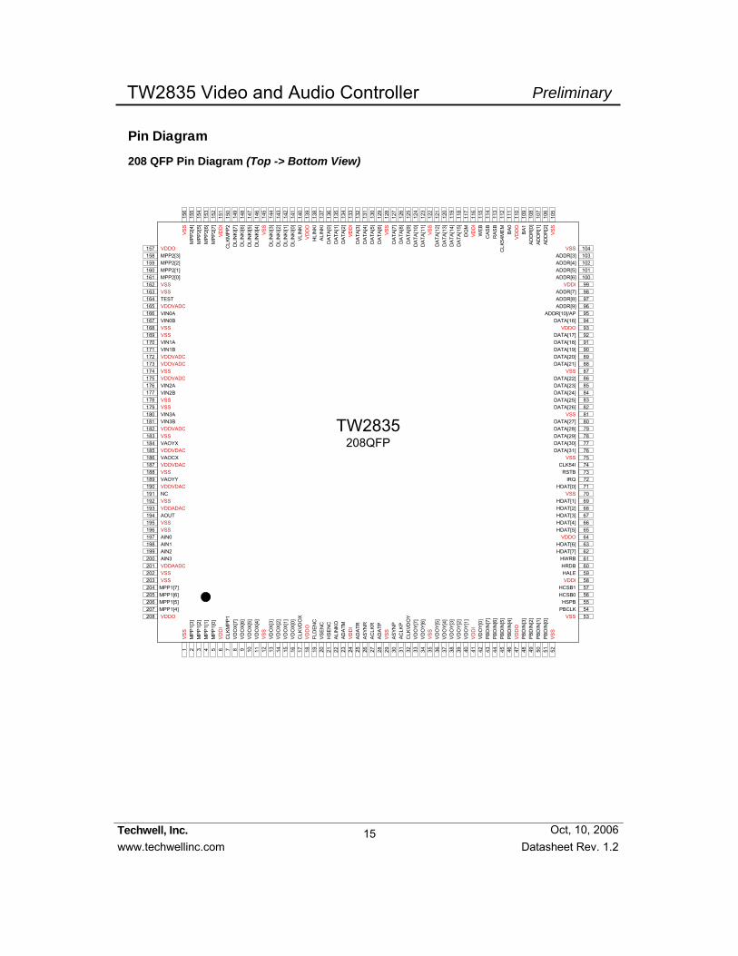
Pin Diagram
208 QFP Pin Diagram (Top -> Bottom View)
TW2835208QFP
VSS
VD
OX[
1]V
DO
X[0]
CLK
VDO
X
VD
DI
HS
EN
CV
SE
NC
FLD
ENC
CLK
VDO
YV
DO
Y[7]
VSS
VD
OY[
6]
VD
OY[
5]V
DO
Y[4]
VD
DO
VD
OY[
3]V
DO
Y[2]
VD
OY[
1]
VDO
Y[0]
VDD
I
VS
S
VS
S
PBD
IN[2
]P
BD
IN[1
]P
BD
IN[0
]
VD
DI
PBCLK
MPP2[0]MPP2[1]MPP2[2]MPP2[3]
VS
S
MP
P2[
4]M
PP
2[5]
MP
P2[
6]
VD
DO
MP
P2[
7]
VD
DI
VS
S
VSS
VDDI
VDDO
VSS
VSS
VDDO
VSS
VD
OX[
2]VD
OX[
3]
VD
OX[
4]V
DO
X[5]
VD
OX[
6]V
DO
X[7]
VDDADAC
NC
AOUT
VSS
VDDVDAC
VDDVADCVS
SV
SS
VD
DI
VD
DO
AD
DR
[2]
AD
DR
[1]
AD
DR
[0]
BA
1
BA
0
RA
SB
CA
SB
WEB
DQ
M
CLK
54M
EM
1 2 3 4 5 6 7 8 9 10 11 12 13 14 15 16 17 18 19 20 21 22 23 24 25 26 27 28 29 30 31 32 33 34 35 36 37 38 39 40 41 42 43 44 45 46 47 48 49 50 51 52V
SS
VSS
VSS
VDDO
VDDI
5354555657585960616263646566676869707172737475767778798081828384858687888990919293949596979899100101102103104VSS
VD
DI
VD
DO
156
155
154
153
152
151
150
149
148
147
146
145
144
143
142
141
140
139
138
137
136
135
134
133
132
131
130
129
128
127
126
125
124
123
122
121
120
119
118
117
116
115
114
113
112
111
110
109
108
107
106
105
VS
S
VSSVSS
VDDVADCVSS
VIN1BVIN1A
VIN0BVIN0A
TESTVDDVADC
PB
DIN
[7]
PB
DIN
[6]
VSS
PB
DIN
[5]
PB
DIN
[4]
PB
DIN
[3]208
207206205204203202201200199198197196195194193192191190189188187186185184183182181180179178177176175174173172171170169168167166165164163162161160159158157 VDDO
DATA[26]
DATA[27]
DATA[29]DATA[28]
DATA[30]DATA[31]
VSS
VSS
AD
ATP
AS
YNP
ACLK
P
ALI
NK
O
AC
LKR
AS
YNR
AD
ATR
ADA
TM
ADDR[10]/APADDR[9]ADDR[8]ADDR[7]
ADDR[6]ADDR[5]ADDR[4]ADDR[3]
DA
TA[1
3]D
ATA
[12]
DA
TA[1
1]D
ATA
[10]
DAT
A[9]
DA
TA[8
]D
ATA[
7]
DAT
A[6]
DAT
A[5]
DAT
A[4]
DAT
A[3]
DA
TA[2
]
DA
TA[1
5]D
ATA
[14]
DATA[24]DATA[25]
DATA[16]
DATA[18]DATA[17]
DATA[19]DATA[20]DATA[21]
DATA[23]DATA[22]
DAT
A[1]
DAT
A[0]
CLK
MP
P2
MPP1[4]MPP1[5]MPP1[6]MPP1[7]
MP
P1[
3]M
PP
1[2]
MP
P1[
1]M
PP
1[0]
CLK
MP
P1D
LIN
KI[7
]D
LIN
KI[6
]D
LIN
KI[5
]D
LIN
KI[4
]
DLI
NK
I[3]
DLI
NK
I[2]
DLI
NK
I[1]
DLI
NK
I[0]
HLI
NK
I
VLI
NK
I
ALI
NK
I
IRQHDAT[0]
HDAT[1]HDAT[2]HDAT[3]HDAT[4]HDAT[5]
HDAT[6]HDAT[7]
HWRBHRDBHALE
HCSB1HCSB0
HSPB
RSTBCLK54I
VSSVSS
VDDVADCVDDVADC
VIN2AVIN2B
VIN3AVIN3B
VSSVAOYX
VAOCX
VAOYYVDDVDAC
VSS
VDDVDAC
VSSVSSAIN0
AIN3
AIN1AIN2
VDDAADC
16
Techwell, Inc. www.techwellinc.com Datasheet Rev. 1.2
PreliminaryTW2835 Video and Audio Controller
Oct, 10, 2006
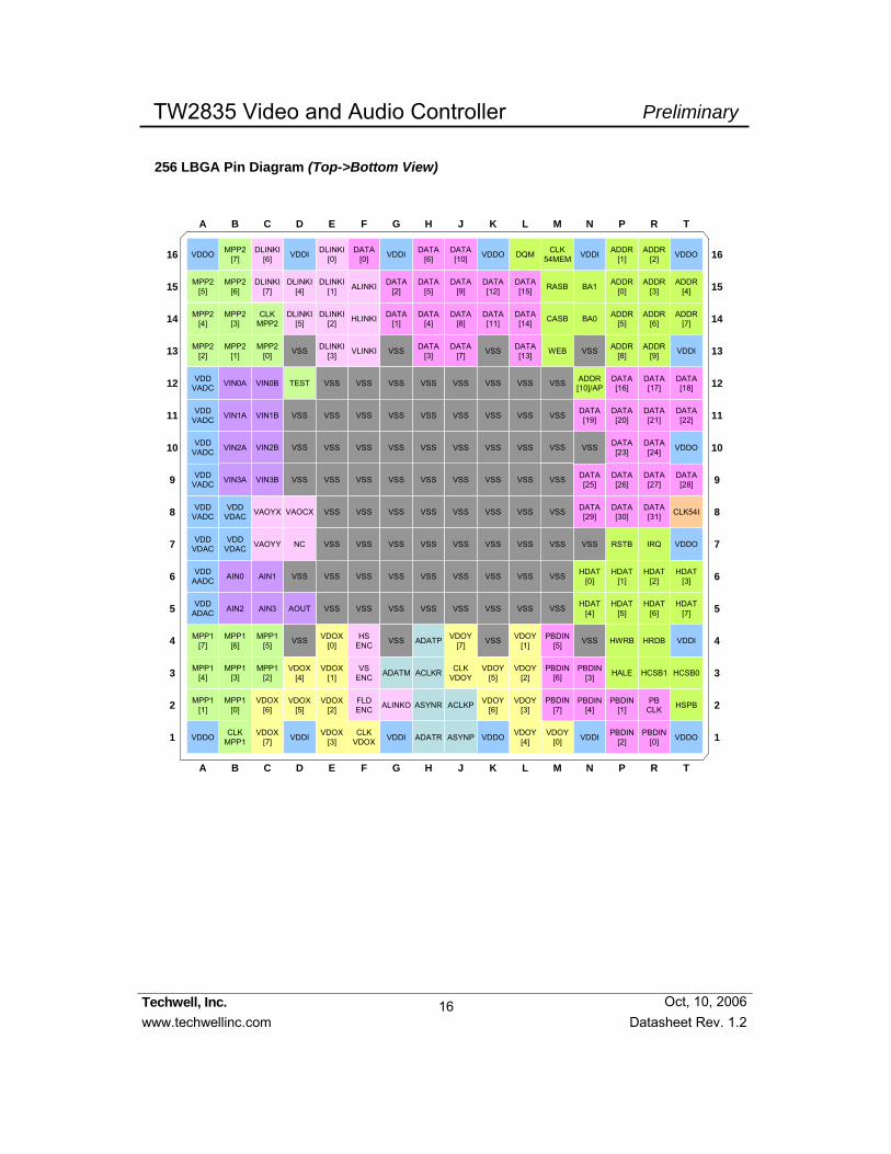
256 LBGA Pin Diagram (Top->Bottom View)
MPP2[7]
DLINKI[7]
DLINKI[4]
DATA[0]
DATA[6]
DATA[10]
DATA[15]
WEB
ADDR[1]
ADDR[2]
ADDR[10]/AP
MPP2[4]
DLINKI[3]
DLINKI[1] ALINKI
DLINKI[6]
DATA[3]
DATA[5]
DATA[9]
DATA[12]
DQM CLK54MEM
BA1 ADDR[0]
ADDR[3]
ADDR[4]
MPP2[3]
MPP2[2]
TEST
DLINKI[0]
HLINKIDLINKI[5]
DATA[7]
DATA[4]
DATA[8]
DATA[1]
DATA[14] CASB BA0 ADDR
[5]ADDR
[6]
MPP2[1]
MPP2[0]
CLKMPP2
VSSVLINKI
DLINKI[2]
VSS
DATA[13]
DATA[11]
VSS
DATA[2] RASB
VSS
ADDR[8]
ADDR[9]
ADDR[7]
MPP2[6]
MPP2[5]
VSS
VSS VSS VSS VSS VSS VSS VSS
DATA[19]
DATA[16]
DATA[17]
VIN1A
VIN0A
VIN2A
VIN0B
VSS
VSS VSS VSS VSS VSS VSS VSS
DATA[23]
DATA[20]
DATA[21]
DATA[22]
VIN3A
VIN1B
VIN3B
VSS
VSS VSS VSS VSS VSS VSS VSS VSS
VSS
DATA[24]
DATA[25]
DATA[18]
VIN2B
VSS
VSS VSS VSS VSS VSS VSS VSS VSS
DATA[29]
DATA[26]
DATA[27]
DATA[28]
VAOYX
VSS
VSS VSS VSS VSS VSS VSS VSS VSS
HSPB
DATA[30]
DATA[31] CLK54IVAOCX
NCVAOYY
VSS
VSS VSS VSS VSS VSS VSS VSS VSS
VSS
RSTB IRQ
HDAT[3]AIN1AIN0 VSS VSS VSS VSS VSS VSS VSS VSS HDAT
[0]HDAT
[1]HDAT
[2]
AIN2 AIN3
CLKMPP1
VSS VSS VSS VSS VSS VSS VSS VSS HDAT[4]
HDAT[5]
HDAT[6]
HDAT[7]AOUT
MPP1[7] VSS
VDOX[7]
VDOX[0]
VSS
ADATM
ASYNP
VSS VDOY[7]
PBDIN[6]
VSS HWRB HRDB
HCSB0
MPP1[5]
MPP1[4]
MPP1[6]
VDOX[6]
VDOX[1]
CLKVDOX
CLKVDOYACLKR
ADATP
VDOY[5]
VDOY[2]
VDOY[0]
PBDIN[3]
PBDIN[7]
HCSB1MPP1[3]
MPP1[2]
MPP1[0]
VDOX[5]
VDOX[2]
FLDENC ALINKO ASYNR ACLKP VDOY
[6]VDOY
[3]
VDOY[1]
PBDIN[4]
PBDIN[1]
PBCLK
HALE
MPP1[1]
VDOX[4]
VDOX[3]
HSENC
ADATR
VSENC
VDOY[4]
PBDIN[5]
PBDIN[2]
PBDIN[0]
16
15
14
13
12
11
10
9
8
7
6
5
4
3
2
1
A B C D E F G H J K L M N P R T
16
15
14
13
12
11
10
9
8
7
6
5
4
3
2
1
A B C D E F G H J K L M N P R T
VDDI VDDI VDDO VDDI VDDOVDDO
VDDI
VDDO
VDDO
VDDI
VDDO VDDI VDDI VDDO VDDI VDDO
VDDAADC
VDDADAC
VDDVADC
VDDVDAC
VDDVDAC
VDDVDAC
VDDVADC
VDDVADC
VDDVADC
VDDVADC
17
Techwell, Inc. www.techwellinc.com Datasheet Rev. 1.2
PreliminaryTW2835 Video and Audio Controller
Oct, 10, 2006
Functional Description
Video Input
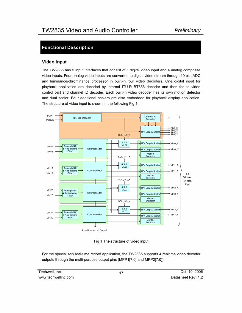
The TW2835 has 5 input interfaces that consist of 1 digital video input and 4 analog composite video inputs. Four analog video inputs are converted to digital video stream through 10 bits ADC and luminance/chrominance processor in built-in four video decoders. One digital input for playback application are decoded by internal ITU-R BT656 decoder and then fed to video control part and channel ID decoder. Each built-in video decoder has its own motion detector and dual scaler. Four additional scalers are also embedded for playback display application. The structure of video input is shown in the following Fig 1.
VIN0B
PBIN
VIN0A
VIN1B
VIN1A
VIN2B
VIN2A
VIN3B
VIN3A
VIN0_X
VIN0_YH/V Crop & Scaler
MotionDetector
H/V Crop & Scaler
ToVideo Control
PartVIN2_X
VIN2_Y
VIN3_X
VIN3_Y
Analog MUX& Anti-aliasing
Filter
4 X 1MUX
4 X 1MUX
4 X 1MUX
4 X 1MUX
H/V Crop & Scaler
Motion Detector
H/V Crop & Scaler
H/V Crop & Scaler
Motion Detector
H/V Crop & Scaler
H/V Crop & Scaler
Motion Detector
H/V Crop & Scaler
VIN1_X
VIN1_Y
Analog MUX& Anti-aliasing
Filter
Analog MUX& Anti-aliasing
Filter
Analog MUX& Anti-aliasing
Filter
4 realtime record Output
BT. 656 Decoder Channel IDDecoder
H/V Crop & ScalerPB0_X
PB3_X
PB1_XPB2_X
Color Decoder
Color Decoder
Color Decoder
Color Decoder
SCL_IN0_X
SCL_IN1_X
SCL_IN2_X
SCL_IN3_X
PBCLK
Fig 1 The structure of video input
For the special 4ch real-time record application, the TW2835 supports 4 realtime video decoder outputs through the multi-purpose output pins (MPP1[7:0] and MPP2[7:0]).

18
Techwell, Inc. www.techwellinc.com Datasheet Rev. 1.2
PreliminaryTW2835 Video and Audio Controller
Oct, 10, 2006
Analog Video Input The TW2835 supports all NTSC/PAL video standards for analog input and contains automatic standard detection circuit. Automatic standard detection can be overridden by writing the value into the IFMTMAN and IFORMAT (0x01, 0x11, 0x21, and 0x31) registers. Even if video loss is detected, the TW2835 can be forced to free-running in a particular video standard mode by IFORMAT register. The Table 1 shows the video input standards supported by TW2835.
Table 1 Video input standards IFORMAT PEDEST Format Line/Fv (Hz) Fh (KHz) Fsc (MHz)
0 PAL-BDGHI 0
1 PAL-N* 625/50 15.625 4.43361875
1 1 PAL-M* 525/59.94 15.734 3.57561149
2 0 PAL-NC 625/50 15.625 3.58205625
3 0 PAL-60 525/59.94 15.734 4.43361875
0 NTSC-J 4
1 NTSC-M* 525/59.94 15.734 3.579545
5 1 NTSC-4.43* 525/59.94 15.734 4.43361875
6 0 NTSC-N 625/50 15.625 3.579545
Notes: * 7.5 IRE Setup
19
Techwell, Inc. www.techwellinc.com Datasheet Rev. 1.2
PreliminaryTW2835 Video and Audio Controller
Oct, 10, 2006
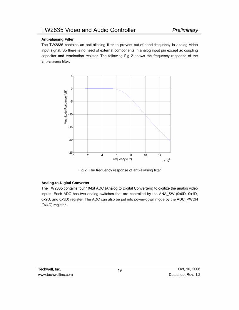
Anti-aliasing Filter The TW2835 contains an anti-aliasing filter to prevent out-of-band frequency in analog video input signal. So there is no need of external components in analog input pin except ac coupling capacitor and termination resistor. The following Fig 2 shows the frequency response of the anti-aliasing filter.
0 2 4 6 8 10 12
x 10 6 -25
-20
-15
-10
-5
0
5
Frequency (Hz)
Mag
nitu
de R
espo
nse
(dB
)
Fig 2. The frequency response of anti-aliasing filter
Analog-to-Digital Converter The TW2835 contains four 10-bit ADC (Analog to Digital Converters) to digitize the analog video inputs. Each ADC has two analog switches that are controlled by the ANA_SW (0x0D, 0x1D, 0x2D, and 0x3D) register. The ADC can also be put into power-down mode by the ADC_PWDN (0x4C) register.
20
Techwell, Inc. www.techwellinc.com Datasheet Rev. 1.2
PreliminaryTW2835 Video and Audio Controller
Oct, 10, 2006
Sync Processing The sync processor of the TW2835 detects horizontal and vertical synchronization signals in the composite video signal. The TW2835 utilizes proprietary technology for locking to weak, noisy, or unstable signals such as those from on air signal or fast forward/backward play of VCR system.
A digital gain and clamp control circuit restores the ac coupled video signal to a fixed dc level. The clamping circuit provides line-by-line restoration of the video pedestal level to a fixed dc reference voltage. In no AGC mode, the gain control circuit adjusts only the video sync gain to achieve desired sync amplitude so that the active video is bypassed regardless of the gain control. But when AGC mode is enabled, both active video and sync are adjusted by the gain control.
The horizontal synchronization processor contains a sync separator, a PLL and the related decision logic. The horizontal sync separator detects the horizontal sync by examining low-pass filtered video input whose level is lower than a threshold. Additional logic is also used to avoid false detection on glitches. The horizontal PLL locks onto the extracted horizontal sync in all conditions to provide jitter free image output. In case of missing horizontal sync, the PLL is on free running status that matches the standard raster frequency.
The vertical sync separator detects the vertical synchronization pattern in the input video signals. The field status is determined at vertical synchronization time. When the location of the detected vertical sync is inline with a horizontal sync, it indicates a frame start or the odd field start. Otherwise, it indicates an even field.
21
Techwell, Inc. www.techwellinc.com Datasheet Rev. 1.2
PreliminaryTW2835 Video and Audio Controller
Oct, 10, 2006
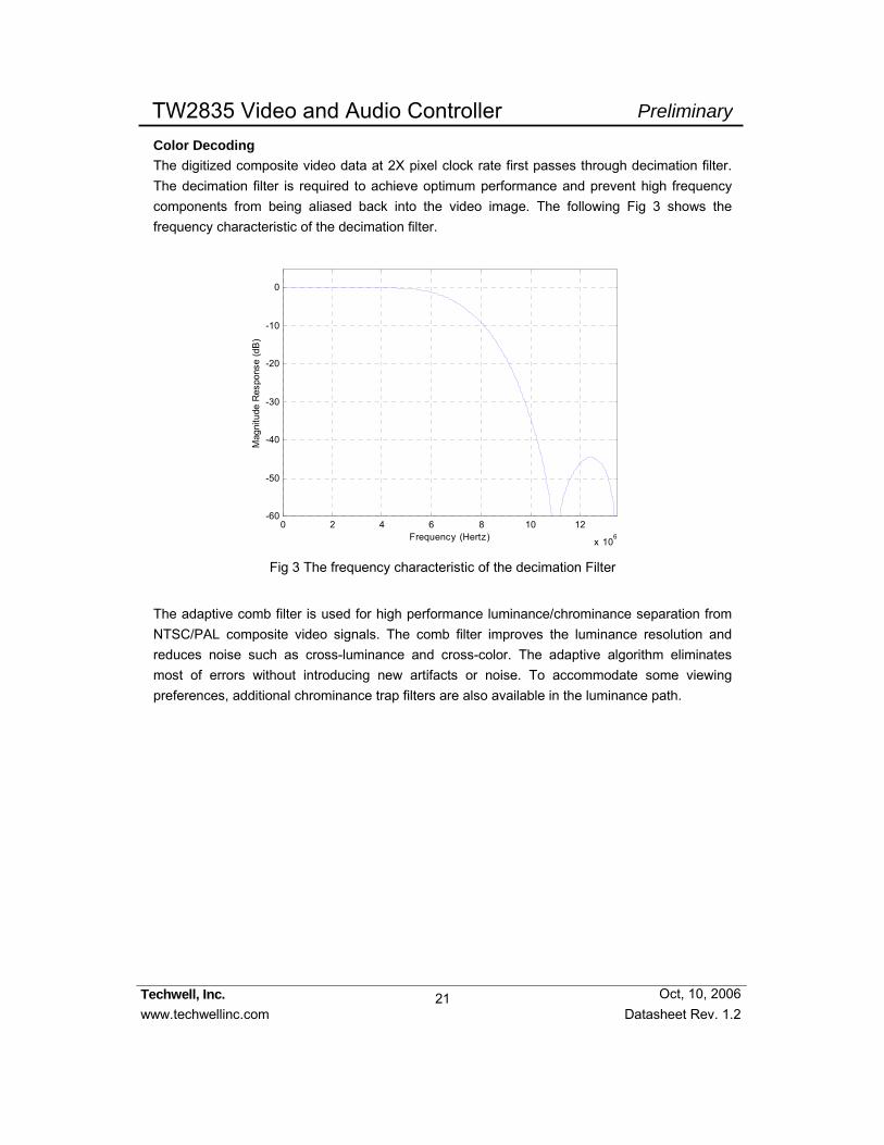
Color Decoding The digitized composite video data at 2X pixel clock rate first passes through decimation filter. The decimation filter is required to achieve optimum performance and prevent high frequency components from being aliased back into the video image. The following Fig 3 shows the frequency characteristic of the decimation filter.
0 2 4 6 8 10 12
x 106
-60
-50
-40
-30
-20
-10
0
Frequency (Hertz)
Mag
nitu
de R
espo
nse
(dB
)
Fig 3 The frequency characteristic of the decimation Filter
The adaptive comb filter is used for high performance luminance/chrominance separation from NTSC/PAL composite video signals. The comb filter improves the luminance resolution and reduces noise such as cross-luminance and cross-color. The adaptive algorithm eliminates most of errors without introducing new artifacts or noise. To accommodate some viewing preferences, additional chrominance trap filters are also available in the luminance path.
22
Techwell, Inc. www.techwellinc.com Datasheet Rev. 1.2
PreliminaryTW2835 Video and Audio Controller
Oct, 10, 2006
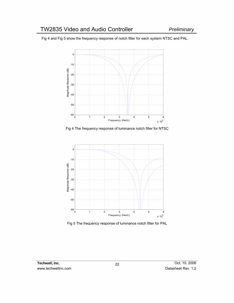
Fig 4 and Fig 5 show the frequency response of notch filter for each system NTSC and PAL.
0 1 2 3 4 5 6
x 106
-60
-50
-40
-30
-20
-10
0
Frequency (Hertz)
Mag
nitu
de R
espo
nse
(dB
)
Fig 4 The frequency response of luminance notch filter for NTSC
0 1 2 3 4 5 6
x 106
-60
-50
-40
-30
-20
-10
0
Frequency (Hertz)
Mag
nitu
de R
espo
nse
(dB
)
Fig 5 The frequency response of luminance notch filter for PAL

23
Techwell, Inc. www.techwellinc.com Datasheet Rev. 1.2
PreliminaryTW2835 Video and Audio Controller
Oct, 10, 2006
Luminance Processing The luminance signal separated by adaptive comb or trap filter is then fed to a peaking circuit. The peaking filter enhances the high frequency components of the luminance signal via the Y_PEAK (0x0B, 0x1B, 0x2B, and 0x3B) register. The following Fig 6 shows the characteristics of the peaking filter for four different gain modes.
0 1 2 3 4 5 6 7
x 106
0
1
2
3
4
5
6
7
8
9
10
Frequency (Hertz)
Mag
nitu
de R
espo
nse
(dB
)
YPEAKMD = 1 YPEAKMD = 0
Fig 6 The frequency characteristic of luminance peaking filter
The picture contrast and brightness adjustment is provided through the CONT (0x09, 0x19, 0x29, and 0x39) and BRT (0x0A, 0x1A, 0x2A, and 0x3A) registers. The contrast adjustment range is from approximately 0 to 200 percent and the brightness adjustment is in the range of ±25 IRE.
24
Techwell, Inc. www.techwellinc.com Datasheet Rev. 1.2
PreliminaryTW2835 Video and Audio Controller
Oct, 10, 2006
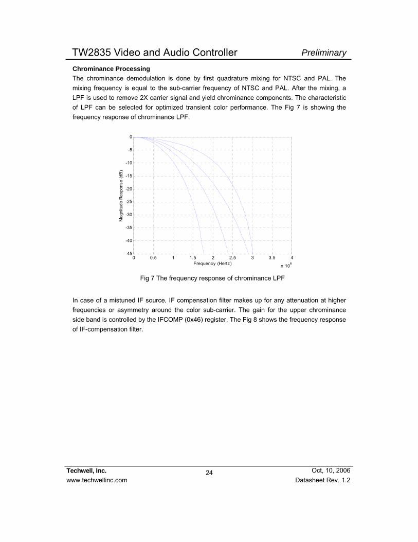
Chrominance Processing The chrominance demodulation is done by first quadrature mixing for NTSC and PAL. The mixing frequency is equal to the sub-carrier frequency of NTSC and PAL. After the mixing, a LPF is used to remove 2X carrier signal and yield chrominance components. The characteristic of LPF can be selected for optimized transient color performance. The Fig 7 is showing the frequency response of chrominance LPF.
0 0.5 1 1.5 2 2.5 3 3.5 4
x 106
-45
-40
-35
-30
-25
-20
-15
-10
-5
0
Frequency (Hertz)
Mag
nitu
de R
espo
nse
(dB
)
Fig 7 The frequency response of chrominance LPF
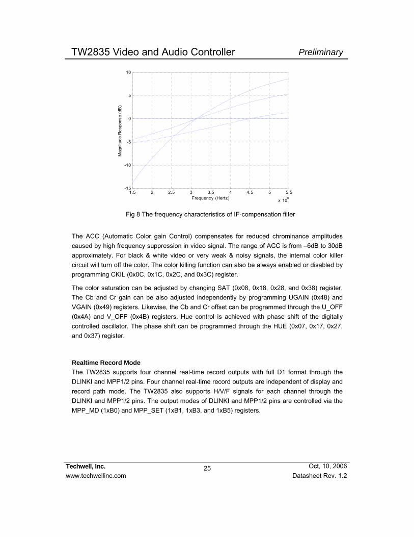
In case of a mistuned IF source, IF compensation filter makes up for any attenuation at higher frequencies or asymmetry around the color sub-carrier. The gain for the upper chrominance side band is controlled by the IFCOMP (0x46) register. The Fig 8 shows the frequency response of IF-compensation filter.
25
Techwell, Inc. www.techwellinc.com Datasheet Rev. 1.2
PreliminaryTW2835 Video and Audio Controller
Oct, 10, 2006
1.5 2 2.5 3 3.5 4 4.5 5 5.5
x 106
-15
-10
-5
0
5
10
Frequency (Hertz)
Mag
nitu
de R
espo
nse
(dB
)
Fig 8 The frequency characteristics of IF-compensation filter
The ACC (Automatic Color gain Control) compensates for reduced chrominance amplitudes caused by high frequency suppression in video signal. The range of ACC is from –6dB to 30dB approximately. For black & white video or very weak & noisy signals, the internal color killer circuit will turn off the color. The color killing function can also be always enabled or disabled by programming CKIL (0x0C, 0x1C, 0x2C, and 0x3C) register.
The color saturation can be adjusted by changing SAT (0x08, 0x18, 0x28, and 0x38) register. The Cb and Cr gain can be also adjusted independently by programming UGAIN (0x48) and VGAIN (0x49) registers. Likewise, the Cb and Cr offset can be programmed through the U_OFF (0x4A) and V_OFF (0x4B) registers. Hue control is achieved with phase shift of the digitally controlled oscillator. The phase shift can be programmed through the HUE (0x07, 0x17, 0x27, and 0x37) register.
Realtime Record Mode The TW2835 supports four channel real-time record outputs with full D1 format through the DLINKI and MPP1/2 pins. Four channel real-time record outputs are independent of display and record path mode. The TW2835 also supports H/V/F signals for each channel through the DLINKI and MPP1/2 pins. The output modes of DLINKI and MPP1/2 pins are controlled via the MPP_MD (1xB0) and MPP_SET (1xB1, 1xB3, and 1xB5) registers.

26
Techwell, Inc. www.techwellinc.com Datasheet Rev. 1.2
PreliminaryTW2835 Video and Audio Controller
Oct, 10, 2006
Digital Video Input The TW2835 supports digital video input with 8bit ITU-R BT.656 standard for playback. This digital input is decoded in built-in ITU-R BT 656 decoder and fed to the scaler block in order to display the scaled video data. The TW2835 supports error correction mode for decoding ITU-R BT.656. The decoded video data are also transferred to channel ID decoder part for auto cropping and strobe function.
Digital Video Input Format The timing of digital video input is illustrated in Fig 9.
PBCLK
PBIN[7:0] Cb0 Y0 Cr080h 10h 80h 10h FFh 00h 00h00h 00h XYFFh XY Y1
EAV code SAV code
Cb2 Y2 Cr2 Y3 Cb4 Y4 Cr4 Y5 Cb6 Y6 Cr6 Y7 Cb8 Y8 Cr8 Y9
Horizontal Blanking Period Horizontal Active Period
Fig 9 Timing diagram of ITU-R BT.656 format for digital video input
The SAV and EAV sequences are shown in Table 2.
Table 2 ITU-R BT.656 SAV and EAV code sequence Condition 656 FVH Value SAV/EAV Code Sequence
Field Vertical Horizontal F V H First Second Third Fourth
EAV 1 0xF1 EVEN Blank
SAV 1 1
0 0xEC EAV 1 0xDA
EVEN Active SAV
1 0 0 0xC7
EAV 1 0xB6 ODD Blank
SAV 0 1
0 0xAB EAV 1 0x9D
ODD Active SAV
0 0 0
0xFF 0x00 0x00
0x80
27
Techwell, Inc. www.techwellinc.com Datasheet Rev. 1.2
PreliminaryTW2835 Video and Audio Controller
Oct, 10, 2006
Channel ID Decoder The TW2835 provides channel ID decoding function for playback input. The TW2835 supports three kinds of channel ID such as User channel ID, Detection channel ID, and auto channel ID. The User channel ID is used for customized information like system information and date. The Detection channel ID is used for detected information of current live input such as motion, video loss, blind and night detection information. The auto channel ID is employed for automatic identification of picture configuration which includes the channel number, analog switch, event, region enable and field/frame mode information. The TW2835 also supports both analog and digital type channel ID during VBI period. The digital channel ID has priority over analog channel ID. The analog type channel ID decoding is enabled via the VBI_ENA (1x86) register and the digital type channel ID decoding is operated via VBI_CODE_EN (1x86) register. Additionally to detect properly the analog channel ID against noise such as VCR source, the channel ID LPF can be enabled via the VBI_FLT_EN (1x86) register. The decoded channel ID information is used for auto cropping / strobe function and can also be read through the host interface. The detailed auto cropping / strobe function for playback input will be described at “Cropping Function” section (page 34) and “Playback Path Control” section (page 57).
For channel ID detection mode, the TW2835 supports both automatic channel ID detection mode and manual channel ID detection mode. For an automatic channel ID detection mode, the playback input should include a run-in clock. But for a manual channel ID detection mode, the playback input can include a run-in clock or not via VBI_RIC_ON (1x88) register. In a manual detection mode, the TW2835 has several related register such as the VBI_PIXEL_HOS (1x87) to define horizontal start offset, the VBI_FLD_OS (1x88) to define line offset between odd and even field, the VBI_PIXEL_HW to define pulse width for 1 bit data, the VBI_LINE_SIZE (1x89) to define channel ID line size and the VBI_LINE_OS (1x89) to define line offset for channel ID. The VBI_MID_VAL (1x8A) register is used to define the threshold level between high and low. Even in automatic channel ID detection mode, the line size and bit width can be discriminated by reading the VBI_LINE_SIZE and VBI_PIXEL_HW (1xCB) register. The Fig 10 shows the relationship between channel ID and register setting.
This channel ID information can be read through the CHID_TYPE or CHID_VALID (1x8B), AUTO_CHID 0/1/2/3 (1x8C~ 1x8F), DET_CHID 0/1/2/3/4/5/6/7 (1x98~1x9F), and USER_CHID 0/1/2/3/4/5/6/7 (1x90~1x97) registers. The CHID_TYPE register discriminates between the Auto channel ID (CHID_TYPE = “1”) and User channel ID (CHID_TYPE = “0”). The CHID_VALID register indicates whether the detected channel ID type is valid or not. The AUTO_CHID, DET_CHID and USER_CHID registers are used to check the decoded channel ID data when the VBI_RD_CTL (1x88) register value is “1”.
Basically the channel ID is located in VBI period and auto strobe and cropping is executed after channel ID decoding. But for some case, the channel ID can be placed in vertical active period instead of VBI period. For this mode, the TW2835 also supports the channel ID decoding

28
Techwell, Inc. www.techwellinc.com Datasheet Rev. 1.2
PreliminaryTW2835 Video and Audio Controller
Oct, 10, 2006
function within vertical active period via the VAV_CHK (1x89) register and manual cropping function via the MAN_PBCROP (0xC0) register with proper VDELAY value.
Run-In Clock
Parity
* Channel ID Type of each line can be detected with Channel ID Type.Auto channel ID = 001 / 010 (Repeated channel ID)Detection Channel ID = 011 / 100User Channel ID = 101 / 110
Analog Channel ID Format
VBI_MID_VAL
Video Output
H
V
FVBI_LINE_OS + VBI_FLD_OS
A0 = 11000000 A1 = 11000001 A2 = 11000010 A2 = 11000010
Channel ID Type (*)
Digital Channel ID
User Channel ID
Detection Channel ID
Auto Channel ID
VBI_PIXEL_WIDTH
VBI_PIXEL_HOS
Fig 10 The related register for manual channel ID detection

29
Techwell, Inc. www.techwellinc.com Datasheet Rev. 1.2
PreliminaryTW2835 Video and Audio Controller
Oct, 10, 2006
Cropping and Scaling Function The TW2835 provides two methods to reduce the amount of video pixel data, scaling and cropping. The scaling function provides video image at lower resolution while the cropping function supplies only a portion of the video image. The TW2835 also supports an auto cropping function for playback input with channel ID decoding. The TW2835 has a free scaler for a variable image size in display path, but has a limitation of image size in record path such as Full / QUAD / CIF format.
Cropping Function for Live The cropping function allows only subsection of a video image to be output. The active video region is determined by the HDELAY, HACTIVE, VDELAY and VACTIVE (0x02 ~ 0x06, 0x12 ~ 0x16, 0x22 ~ 0x26, 0x32 ~ 0x36) register. The first active line is defined by the VDELAY register and the first active pixel is defined by the HDELAY register. The VACTIVE register can be programmed to define the number of active lines in a video field, and the HACTIVE register can be programmed to define the number of active pixels in a video line. This function is used to implement for panning and tilt.
The horizontal delay register HDELAY determines the number of pixel delays between the horizontal reference and the leading edge of the active region. The horizontal active register HACTIVE determines the number of active pixels to be processed. Note that these values are referenced to the pixel number before scaling. Therefore, even if the scaling ratio is changed, the active video region used for scaling remains unchanged as set by the HDEALY and HACTIVE register. In order for the cropping to work properly, the following equation should be satisfied.
HDELAY + HACTIVE < Total number of pixels per line
Where the total number of pixels per line is 858 for NTSC and 864 for PAL
To process full size region, the HDELAY should be set to 32 and HACTIVE set to 720 for both NTSC and PAL system.
The vertical delay register (VDELAY) determines the number of line delays from the vertical reference to the start of the active video lines. The vertical active register (VACTIVE) determines the number of lines to be processed. These values are referenced to the incoming scan lines before the vertical scaling. In order for the vertical cropping to work properly, the following equation should be satisfied.
VDELAY + VACTIVE < Total number of lines per field
Where the total number of lines per field is 262 for NTSC and 312 for PAL
To process full size region, the VDELAY should be set to 6 and VACTIVE set to 240 for NTSC and the VDELAY should be also set to 5 and VACTIVE set to 288 for PAL.
30
Techwell, Inc. www.techwellinc.com Datasheet Rev. 1.2
PreliminaryTW2835 Video and Audio Controller
Oct, 10, 2006
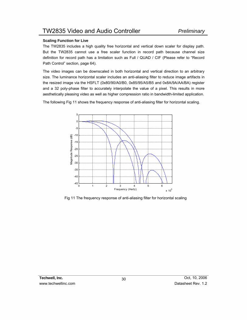
Scaling Function for Live The TW2835 includes a high quality free horizontal and vertical down scaler for display path. But the TW2835 cannot use a free scaler function in record path because channel size definition for record path has a limitation such as Full / QUAD / CIF (Please refer to “Record Path Control” section, page 64).
The video images can be downscaled in both horizontal and vertical direction to an arbitrary size. The luminance horizontal scaler includes an anti-aliasing filter to reduce image artifacts in the resized image via the HSFLT (0x80/90/A0/B0, 0x85/95/A5/B5 and 0x8A/9A/AA/BA) register and a 32 poly-phase filter to accurately interpolate the value of a pixel. This results in more aesthetically pleasing video as well as higher compression ratio in bandwidth-limited application.
The following Fig 11 shows the frequency response of anti-aliasing filter for horizontal scaling.
0 1 2 3 4 5 6
x 106
-45
-40
-35
-30
-25
-20
-15
-10
-5
0
5
Mag
nitu
de R
espo
nse
(dB
)
Frequency (Hertz)
Fig 11 The frequency response of anti-aliasing filter for horizontal scaling

31
Techwell, Inc. www.techwellinc.com Datasheet Rev. 1.2
PreliminaryTW2835 Video and Audio Controller
Oct, 10, 2006
Similarly, the vertical scaler also contains an anti-aliasing filter controlled via the VSFLT (0x80/90/A0/B0, 0x85/95/A5/B5 and 0x8A/9A/AA/BA) register and 16 poly-phase filters for down scaling. The filter characteristics are shown in the Fig 12.
0 0.05 0.1 0.15 0.2 0.25 0.3 0.35 0.4 0.45 0.5-40
-35
-30
-25
-20
-15
-10
-5
0
Mag
nitu
de R
espo
nse
(dB
)
Frequency (Hertz)
Fig 12 The characteristics of anti-aliasing filter for vertical scaling

32
Techwell, Inc. www.techwellinc.com Datasheet Rev. 1.2
PreliminaryTW2835 Video and Audio Controller
Oct, 10, 2006
Down scaling is achieved by programming the scaling register HSCALE and VSCALE (0x81 ~ 0x84, 0x91 ~ 0x94, 0xA1 ~ 0xA4, 0xB1 ~ 0xB4) register. When no scaled video image, the TW2835 will output the number of pixels as specified by the HACTIVE and VACTIVE (0x02 ~ 0x06, 0x12 ~ 0x16, 0x22 ~ 0x26, 0x32 ~ 0x36) register. If the number of output pixels required is smaller than the number specified by the HACTIVE/VACTIVE register, the 16bit HSCALE/ VSCALE register is used to reduce the output pixels to the desired number.
The following equation is used to determine the horizontal scaling ratio to be written into the 16bit HSCALE register.
HSCALE = [Npixel_desired/ HACTIVE] * (2^16 – 1)
Where Npixel_desired is the desired number of active pixels per line
For example, to scale picture from full size (HACTIVE = 720) to CIF (360 pixels), the HSCALE value can be found as:
HSCALE = [360/720] * (2^16 – 1) = 0x7FFF
The following equation is used to determine the vertical scaling ratio to be written into the 16bit VSCALE register.
VSCALE = [Nline_desired / VACTIVE] * (2^16 - 1)
Where Nline_desired is the desired number of active lines per field
For example, to scale picture from full size (VACTIVE = 240 lines for NTSC and 288 lines for PAL) to CIF (120 lines for NTSC and 144 lines for PAL), the VSCALE value can be found as:
VSCALE = [120 / 240] * (2^16 – 1) = 0x7FFF for NTSC
VSCALE = [144 / 288] * (2^16 – 1) = 0x7FFF for PAL
The scaling ratios of popular case are listed in Table 3.
Table 3 HSCALE and VSCALE value for popular video formats Scaling Ratio Format Output Resolution HSCALE VSCALE
1 NTSC PAL
720x480 720x576
0xFFFF 0xFFFF
0xFFFF 0xFFFF
1/2 (CIF) NTSC PAL
360x240 360x288
0x7FFF 0x7FFF
0x7FFF 0x7FFF
1/4 (QCIF) NTSC PAL
180x120 180x144
0x3FFF 0x3FFF
0x3FFF 0x3FFF

33
Techwell, Inc. www.techwellinc.com Datasheet Rev. 1.2
PreliminaryTW2835 Video and Audio Controller
Oct, 10, 2006
The effect of scaling and cropping is shown in Fig 13.
VA
CTI
VE
* V
SC
ALE
HACTIVE * HSCALE Cropping and Scaling
VD
ELA
YVA
CTI
VE
HDELAY HACTIVE
V reference
H reference
VD
ELA
YVA
CTI
VE
HDELAY HACTIVE
V reference
H reference
Fig 13 The effect of cropping and scaling
34
Techwell, Inc. www.techwellinc.com Datasheet Rev. 1.2
PreliminaryTW2835 Video and Audio Controller
Oct, 10, 2006
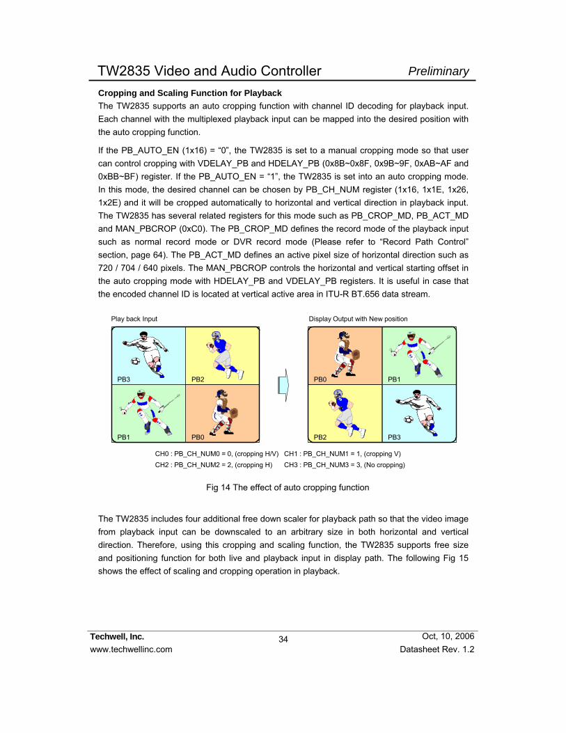
Cropping and Scaling Function for Playback The TW2835 supports an auto cropping function with channel ID decoding for playback input. Each channel with the multiplexed playback input can be mapped into the desired position with the auto cropping function.
If the PB_AUTO_EN (1x16) = “0”, the TW2835 is set to a manual cropping mode so that user can control cropping with VDELAY_PB and HDELAY_PB (0x8B~0x8F, 0x9B~9F, 0xAB~AF and 0xBB~BF) register. If the PB_AUTO_EN = “1”, the TW2835 is set into an auto cropping mode. In this mode, the desired channel can be chosen by PB_CH_NUM register (1x16, 1x1E, 1x26, 1x2E) and it will be cropped automatically to horizontal and vertical direction in playback input. The TW2835 has several related registers for this mode such as PB_CROP_MD, PB_ACT_MD and MAN_PBCROP (0xC0). The PB_CROP_MD defines the record mode of the playback input such as normal record mode or DVR record mode (Please refer to “Record Path Control” section, page 64). The PB_ACT_MD defines an active pixel size of horizontal direction such as 720 / 704 / 640 pixels. The MAN_PBCROP controls the horizontal and vertical starting offset in the auto cropping mode with HDELAY_PB and VDELAY_PB registers. It is useful in case that the encoded channel ID is located at vertical active area in ITU-R BT.656 data stream.
Play back Input Display Output with New position
PB3
PB1 PB0
PB2 PB0
PB2 PB3
PB1
CH0 : PB_CH_NUM0 = 0, (cropping H/V) CH1 : PB_CH_NUM1 = 1, (cropping V)CH2 : PB_CH_NUM2 = 2, (cropping H) CH3 : PB_CH_NUM3 = 3, (No cropping)
Fig 14 The effect of auto cropping function
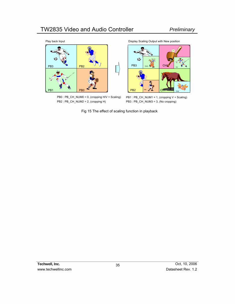
The TW2835 includes four additional free down scaler for playback path so that the video image from playback input can be downscaled to an arbitrary size in both horizontal and vertical direction. Therefore, using this cropping and scaling function, the TW2835 supports free size and positioning function for both live and playback input in display path. The following Fig 15 shows the effect of scaling and cropping operation in playback.
35
Techwell, Inc. www.techwellinc.com Datasheet Rev. 1.2
PreliminaryTW2835 Video and Audio Controller
Oct, 10, 2006
Play back Input Display Scaling Output with New position
PB3
PB1 PB0
PB2
PB2
PB0 : PB_CH_NUM0 = 0, (cropping H/V + Scaling) PB1 : PB_CH_NUM1 = 1, (cropping V + Scaling)PB2 : PB_CH_NUM2 = 2, (cropping H) PB3 : PB_CH_NUM3 = 3, (No cropping)
PB1PB3
PB0
Ch0
Ch1 Ch2
Ch3
Fig 15 The effect of scaling function in playback

36
Techwell, Inc. www.techwellinc.com Datasheet Rev. 1.2
PreliminaryTW2835 Video and Audio Controller
Oct, 10, 2006
Motion Detection
The TW2835 supports motion detector individually for 4 analog video inputs. The built-in motion detection algorithm uses the difference of luminance level between current and reference field. The TW2835 also supports blind and night input detection for 4 analog video inputs.
To detect motion properly according to situation, the TW2835 provides several sensitivity and velocity control parameters for each motion detector. The TW2835 supports manual strobe function to update motion detection so that it is more appropriate for user-defined motion sensitivity control.
When motion, blind and night input are detected in any video inputs, the TW2835 provides the interrupt request to host via the IRQ pin. The host processor can take the information of motion, blind or night detection by accessing the IRQENA_MD (1x79), IRQENA_BD (1x7A) and the IRQENA_ND (1x7B) register. This status information is updated in the vertical blank period of each input.
The TW2835 also provides the motion, blind and night detection result through the DLINKI and MPP0/1 pin with the control of MPP_MD (1xB0) and MPP_SET (1xB1, 1xB3 and 1xB5) register. The TW2835 supports an overlay function to display the motion detection result in the picture with 2D arrayed box.

37
Techwell, Inc. www.techwellinc.com Datasheet Rev. 1.2
PreliminaryTW2835 Video and Audio Controller
Oct, 10, 2006
Mask and Detection Region Selection The motion detection algorithm utilizes the full screen video data and detects individual motion of 16x12 cells. This full screen for motion detection consists of 704 pixels and 240 lines for NTSC and 288 lines for PAL. Starting pixel in horizontal direction can be shifted from 0 to 15 pixels using the MD_ALIGN (2x82, 2xA2, 2xC2, and 2xE2) register.
Each cell can be masked via the MD_MASK (2x86 ~ 2x9D, 2xA6 ~ 2xBD, 2xC6 ~ 2xDD, 2xE6 ~ 2xFD) register as illustrated in Fig 16. If the mask bit in specific cell is programmed to high, the related cell is ignored for motion detection.
240
Line
s fo
r 60H
z (2
0 Li
nes/
Cel
l), 2
88 L
ines
for 5
0Hz
(24
Line
s/C
ell)
704 Pixels (44 Pixels/Cell)
MD_ MASK11
[15]
MD_ MASK11
[14]
MD_ MASK11
[13]
MD_ MASK11
[12]
MD_ MASK11
[11]
MD_ MASK11
[10]
MD_ MASK11
[9]
MD_ MASK11
[8]
MD_ MASK11
[7]
MD_ MASK11
[6]
MD_ MASK11
[5]
MD_ MASK11
[4]
MD_ MASK11
[3]
MD_ MASK11
[2]
MD_ MASK11
[1]
MD_ MASK11
[0]
MD_ MASK10
[15]
MD_ MASK10
[14]
MD_ MASK10
[13]
MD_ MASK10
[12]
MD_ MASK10
[11]
MD_ MASK10
[10]
MD_ MASK10
[9]
MD_ MASK10
[8]
MD_ MASK10
[7]
MD_ MASK10
[6]
MD_ MASK10
[5]
MD_ MASK10
[4]
MD_ MASK10
[3]
MD_ MASK10
[2]
MD_ MASK10
[1]
MD_ MASK10
[0]
MD_ MASK9
[15]
MD_ MASK9
[14]
MD_ MASK9
[13]
MD_ MASK9
[12]
MD_ MASK9
[11]
MD_ MASK9
[10]
MD_ MASK9
[9]
MD_ MASK9
[8]
MD_ MASK9
[7]
MD_ MASK9
[6]
MD_ MASK9
[5]
MD_ MASK9
[4]
MD_ MASK9
[3]
MD_ MASK9
[2]
MD_ MASK9
[1]
MD_ MASK9
[0]
MD_ MASK8
[15]
MD_ MASK8
[14]
MD_ MASK8
[13]
MD_ MASK8
[12]
MD_ MASK8
[11]
MD_ MASK8
[10]
MD_ MASK8
[9]
MD_ MASK8
[8]
MD_ MASK8
[7]
MD_ MASK8
[6]
MD_ MASK8
[5]
MD_ MASK8
[4]
MD_ MASK8
[3]
MD_ MASK8
[2]
MD_ MASK8
[1]
MD_ MASK8
[0]
MD_ MASK7
[15]
MD_ MASK7
[14]
MD_ MASK7
[13]
MD_ MASK7
[12]
MD_ MASK7
[11]
MD_ MASK7
[10]
MD_ MASK7
[9]
MD_ MASK7
[8]
MD_ MASK7
[7]
MD_ MASK7
[6]
MD_ MASK7
[5]
MD_ MASK7
[4]
MD_ MASK7
[3]
MD_ MASK7
[2]
MD_ MASK7
[1]
MD_ MASK7
[0]
MD_ MASK6
[15]
MD_ MASK6
[14]
MD_ MASK6
[13]
MD_ MASK6
[12]
MD_ MASK6
[11]
MD_ MASK6
[10]
MD_ MASK6
[9]
MD_ MASK6
[8]
MD_ MASK6
[7]
MD_ MASK6
[6]
MD_ MASK6
[5]
MD_ MASK6
[4]
MD_ MASK6
[3]
MD_ MASK6
[2]
MD_ MASK6
[1]
MD_ MASK6
[0]
MD_ MASK5
[15]
MD_ MASK5
[14]
MD_ MASK5
[13]
MD_ MASK5
[12]
MD_ MASK5
[11]
MD_ MASK5
[10]
MD_ MASK5
[9]
MD_ MASK5
[8]
MD_ MASK5
[7]
MD_ MASK5
[6]
MD_ MASK5
[5]
MD_ MASK5
[4]
MD_ MASK5
[3]
MD_ MASK5
[2]
MD_ MASK5
[1]
MD_ MASK5
[0]
MD_ MASK4
[15]
MD_ MASK4
[14]
MD_ MASK4
[13]
MD_ MASK4
[12]
MD_ MASK4
[11]
MD_ MASK4
[10]
MD_ MASK4
[9]
MD_ MASK4
[8]
MD_ MASK4
[7]
MD_ MASK4
[6]
MD_ MASK4
[5]
MD_ MASK4
[4]
MD_ MASK4
[3]
MD_ MASK4
[2]
MD_ MASK4
[1]
MD_ MASK4
[0]
MD_ MASK3
[15]
MD_ MASK3
[14]
MD_ MASK3
[13]
MD_ MASK3
[12]
MD_ MASK3
[11]
MD_ MASK3
[10]
MD_ MASK3
[9]
MD_ MASK3
[8]
MD_ MASK3
[7]
MD_ MASK3
[6]
MD_ MASK3
[5]
MD_ MASK3
[4]
MD_ MASK3
[3]
MD_ MASK3
[2]
MD_ MASK3
[1]
MD_ MASK3
[0]
MD_ MASK2
[15]
MD_ MASK2
[14]
MD_ MASK2
[13]
MD_ MASK2
[12]
MD_ MASK2
[11]
MD_ MASK2
[10]
MD_ MASK2
[9]
MD_ MASK2
[8]
MD_ MASK2
[7]
MD_ MASK2
[6]
MD_ MASK2
[5]
MD_ MASK2
[4]
MD_ MASK2
[3]
MD_ MASK2
[2]
MD_ MASK2
[1]
MD_ MASK2
[0]
MD_ MASK1
[15]
MD_ MASK1
[14]
MD_ MASK1
[13]
MD_ MASK1
[12]
MD_ MASK1
[11]
MD_ MASK1
[10]
MD_ MASK1
[9]
MD_ MASK1
[8]
MD_ MASK1
[7]
MD_ MASK1
[6]
MD_ MASK1
[5]
MD_ MASK1
[4]
MD_ MASK1
[3]
MD_ MASK1
[2]
MD_ MASK1
[1]
MD_ MASK1
[0]
MD_ MASK0
[15]
MD_ MASK0
[14]
MD_ MASK0
[13]
MD_ MASK0
[12]
MD_ MASK0
[11]
MD_ MASK0
[10]
MD_ MASK0
[9]
MD_ MASK0
[8]
MD_ MASK0
[7]
MD_ MASK0
[6]
MD_ MASK0
[5]
MD_ MASK0
[4]
MD_ MASK0
[3]
MD_ MASK0
[2]
MD_MASK0
[1]
MD_ MASK0
[0]
Fig 16 Motion mask and detection cell
The MD_MASK register has different function for reading and writing mode. For writing mode, setting “1” to MD_MASK register inhibits the specific cell from detecting motion. For reading mode, the MD_MASK register has three kinds of information depending on the MASK_MODE (2x82, 2xA2, 2xC2, and 2xE2) register. For MASK_MODE = “0”, the state of MD_MASK register means the result of VIN_A motion detection that “1” indicates detecting motion and “0” denotes no motion detection in the cell. For MASK_MODE = “1”, the state of MD_MASK register means the result of VIN_B motion detection. For MASK_MODE = “2 or 3”, the state of MD_MASK register means masking information of cell.
38
Techwell, Inc. www.techwellinc.com Datasheet Rev. 1.2
PreliminaryTW2835 Video and Audio Controller
Oct, 10, 2006
Sensitivity Control The motion detector has 4 sensitivity parameters to control threshold of motion detection such as the level sensitivity via the MD_LVSENS (2x83, 2xA3, 2xC3, and 2xE3) register, the spatial sensitivity via the MD_SPSENS (2x85, 2xA5, 2xC5, 2xE5) and MD_CELSENS (2x83, 2xA3, 2xC3, and 2xE3) register, and the temporal sensitivity parameter via the MD_TMPSENS (2x85, 2xA5, 2xC5, and 2xE5) register.
Level Sensitivity In built-in motion detection algorithm, the motion is detected when luminance level difference between current and reference field is greater than MD_LVSENS value. Motion detector is more sensitive for the smaller MD_LVSENS value and less sensitive for the larger. When the MD_LVSENS is too small, the motion detector may be weak in noise.
Spatial Sensitivity The TW2835 uses 192 (16x12) detection cells in full screen for motion detection. Each detection cell is composed of 44 pixels and 20 lines for NTSC and 24 lines for PAL. Motion detection from only luminance level difference between two fields is very weak in spatial random noise. To remove the fake motion detection from the random noise, the TW2835 supports a spatial filter via the MD_SPSENS register which defines the number of detected cell to decide motion detection in full size image. The large MD_SPSENS value increases the immunity of spatial random noise.
Each detection cell has 4 sub-cells also. Actually motion detection of each cell comes from comparison of sub-cells in it. The MD_CELSENS defines the number of detected sub-cell to decide motion detection in cell. That is, the large MD_CELSENS value increases the immunity of spatial random noise in detection cell.
Temporal Sensitivity Similarly, temporal filter is used to remove the fake motion detection from the temporal random noise. The MD_TMPSENS regulates the number of taps in the temporal filter to control the temporal sensitivity so that the large MD_TMPSENS value increases the immunity of temporal random noise.
39
Techwell, Inc. www.techwellinc.com Datasheet Rev. 1.2
PreliminaryTW2835 Video and Audio Controller
Oct, 10, 2006
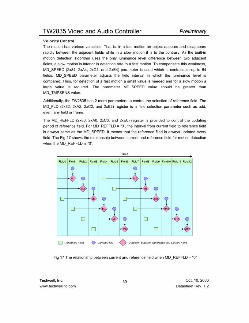
Velocity Control The motion has various velocities. That is, in a fast motion an object appears and disappears rapidly between the adjacent fields while in a slow motion it is to the contrary. As the built-in motion detection algorithm uses the only luminance level difference between two adjacent fields, a slow motion is inferior in detection rate to a fast motion. To compensate this weakness, MD_SPEED (2x84, 2xA4, 2xC4, and 2xE4) parameter is used which is controllable up to 64 fields. MD_SPEED parameter adjusts the field interval in which the luminance level is compared. Thus, for detection of a fast motion a small value is needed and for a slow motion a large value is required. The parameter MD_SPEED value should be greater than MD_TMPSENS value.
Additionally, the TW2835 has 2 more parameters to control the selection of reference field. The MD_FLD (2x82, 2xA2, 2xC2, and 2xE2) register is a field selection parameter such as odd, even, any field or frame.
The MD_REFFLD (2x80, 2xA0, 2xC0, and 2xE0) register is provided to control the updating period of reference field. For MD_REFFLD = “0”, the interval from current field to reference field is always same as the MD_SPEED. It means that the reference filed is always updated every field. The Fig 17 shows the relationship between current and reference field for motion detection when the MD_REFFLD is “0”.
Field0
M1
Field1 Field2 Field3
M2
M3
M4
M5
M6
Field4 Field5 Field6 Field7 Field8 Field9 Field10 Field11 Field12
M7
M8
M9
M10
M11
M12
Time
Reference Field Detection between Reference and Current FieldCurrent Field
Fig 17 The relationship between current and reference field when MD_REFFLD = “0”

40
Techwell, Inc. www.techwellinc.com Datasheet Rev. 1.2
PreliminaryTW2835 Video and Audio Controller
Oct, 10, 2006
The TW2835 can update the reference field only at the period of MD_SPEED when the MD_REFFLD is high. For this case, the TW2835 can detect a motion with sense of a various velocity. The Fig 18 shows the relationship between current and reference field for motion detection when the MD_REFFLD = ”1”.
Field0
M1
Field1 Field2 Field3
M2
M3
M4
M5
M6
Field4 Field5 Field6 Field7 Field8 Field9 Field10 Field11 Field12
M7
M8
M9
M10
M11
M12
Time
Reference Field Detection between Reference and Current FieldCurrent Field
Fig 18 The relationship between current and reference field when MD_REFFLD = “1”
The TW2835 also supports the manual detection timing control of the reference field/frame via the MD_STRB_EN and MD_STRB (2x84, 2xA4, 2xC4, and 2xE4) register. For MD_STRB_EN = “0”, the reference field/frame is automatically updated and reserved on every reference field/frame. For MD_STRB_EN = “1”, the reference field/frame is updated and reserved only when MD_STRB = “1”. In this mode, the interval between current and reference field/frame depends on user’s strobe timing. This mode is very useful for a specific purpose like non-periodical velocity control and very slow motion detection.
The TW2835 also provides dual detection mode for non-realtime application such as pseudo-8ch application via MD_DUAL_EN (2x83, 2xA3, 2xC3, and 2xE3) register. For MD_DUAL_EN = 1, the TW2835 can detect dual motion independently for VIN_A and B Input which is defined by the ANA_SW (0x0D, 0x1D, 0x2D, and 0x3D) register. In this case, the MD_SPEED is limited to 31. These motion information can be read via the IRQENA_MD (1x79) register by the host interface.
41
Techwell, Inc. www.techwellinc.com Datasheet Rev. 1.2
PreliminaryTW2835 Video and Audio Controller
Oct, 10, 2006
Blind Detection The TW2835 supports blind detection individually for 4 analog video inputs and makes an interrupt of blind detection to host. If video level in wide area of field is almost equal to average video level of field due to camera shaded by something, this input is defined as blind input.
The TW2835 has two sensitivity parameters to detect blind input such as the level sensitivity via the BD_LVSENS (2x80, 2xA0, 2xC0, and 2xE0) register and spatial sensitivity via the BD_CELSENS (2x80, 2xA0, 2xC0, and 2xE0) register.
The TW2835 uses total 768 (32x24) cells in full screen for blind detection. The BD_LVSENS parameter controls the threshold of level between cell and field average. The BD_CELSENS parameter defines the number of cells to detect blind. For BD_CELSENS = “0”, the number of cell whose level is same as average of field should be over than 60% to detect blind, 70% for BD_CELSENS = “1”, 80% for BD_CELSENS = “2”, and 90% for BD_CELSENS = “3”. That is, the large value of BD_LVSENS and BD_CELSENS makes blind detector less sensitive.
The TW2835 also supports dual detection mode for non-realtime application such as pseudo-8ch application via the MD_DUAL_EN (2x83, 2xA3, 2xC3, and 2xE3) register. The host can read blind detection information for both VIN_A and VIN_B input via the IRQENA_BD (1x7A) register.
Night Detection The TW2835 supports night detection individually for 4 analog video inputs and makes an interrupt of night detection to host. If an average of field video level is very low, this input is defined as night input. Likewise, the opposite is defined as day input.
The TW2835 has two sensitivity parameters to detect night input such as the level sensitivity via the ND_LVSENS (2x81, 2xA1, 2xC1, and 2xE1) register and the temporal sensitivity via the ND_TMPSENS (2x81, 2xA1, 2xC1, and 2xE1) register. The ND_LVSENS parameter controls threshold level of day and night. The ND_TMPSENS parameter regulates the number of taps in the temporal low pass filter to control the temporal sensitivity. The large value of ND_LVSENS and ND_TMPSENS makes night detector less sensitive.
The TW2835 also supports dual detection mode for non-realtime application such as pseudo-8ch application via the MD_DUAL_EN (2x83, 2xA3, 2xC3, and 2xE3) register. The host can read night detection information for both VIN_A and VIN_B input via the IRQENA_ND (1x7B) register.
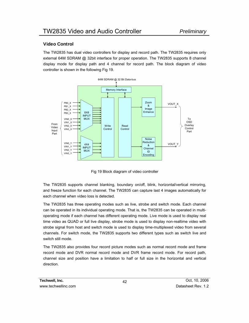
42
Techwell, Inc. www.techwellinc.com Datasheet Rev. 1.2
PreliminaryTW2835 Video and Audio Controller
Oct, 10, 2006
Video Control
The TW2835 has dual video controllers for display and record path. The TW2835 requires only external 64M SDRAM @ 32bit interface for proper operation. The TW2835 supports 8 channel display mode for display path and 4 channel for record path. The block diagram of video controller is shown in the following Fig 19.
WriteControl
Memory Interface
64M SDRAM @ 32 Bit Data-bus
Zoom&
ImageEnhance
VOUT_X
VOUT_Y
To OSD
OverlayControl
Part
PB0_XPB1_XPB2_XPB3_X
4X4INPUTMUX
From VideoInputPart
NoiseReduction
&Channel
IDEncoding
ReadControl
VIN0_XVIN1_XVIN2_XVIN3_X
VIN0_YVIN1_YVIN2_YVIN3_Y
8X8INPUTMUX
Fig 19 Block diagram of video controller
The TW2835 supports channel blanking, boundary on/off, blink, horizontal/vertical mirroring, and freeze function for each channel. The TW2835 can capture last 4 images automatically for each channel when video loss is detected.
The TW2835 has three operating modes such as live, strobe and switch mode. Each channel can be operated in its individual operating mode. That is, the TW2835 can be operated in multi-operating mode if each channel has different operating mode. Live mode is used to display real time video as QUAD or full live display, strobe mode is used to display non-realtime video with strobe signal from host and switch mode is used to display time-multiplexed video from several channels. For switch mode, the TW2835 supports two different types such as switch live and switch still mode.
The TW2835 also provides four record picture modes such as normal record mode and frame record mode and DVR normal record mode and DVR frame record mode. For record path, channel size and position have a limitation to half or full size in the horizontal and vertical direction.
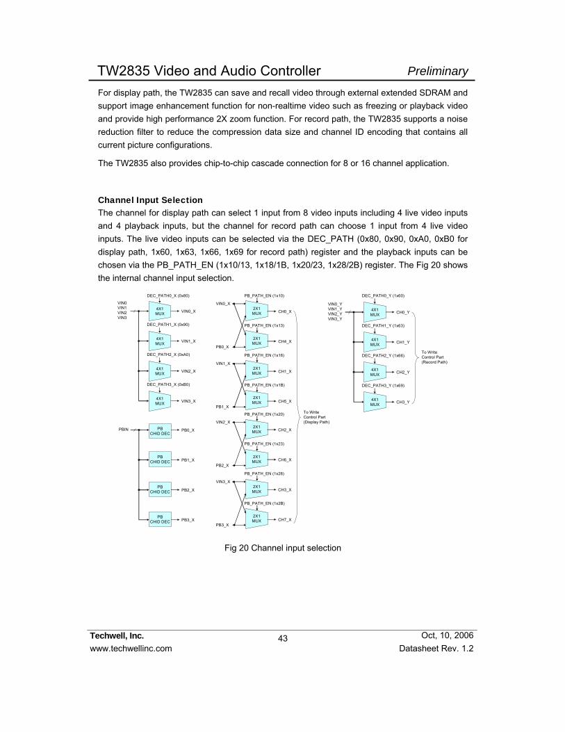
43
Techwell, Inc. www.techwellinc.com Datasheet Rev. 1.2
PreliminaryTW2835 Video and Audio Controller
Oct, 10, 2006
For display path, the TW2835 can save and recall video through external extended SDRAM and support image enhancement function for non-realtime video such as freezing or playback video and provide high performance 2X zoom function. For record path, the TW2835 supports a noise reduction filter to reduce the compression data size and channel ID encoding that contains all current picture configurations.
The TW2835 also provides chip-to-chip cascade connection for 8 or 16 channel application.
Channel Input Selection The channel for display path can select 1 input from 8 video inputs including 4 live video inputs and 4 playback inputs, but the channel for record path can choose 1 input from 4 live video inputs. The live video inputs can be selected via the DEC_PATH (0x80, 0x90, 0xA0, 0xB0 for display path, 1x60, 1x63, 1x66, 1x69 for record path) register and the playback inputs can be chosen via the PB_PATH_EN (1x10/13, 1x18/1B, 1x20/23, 1x28/2B) register. The Fig 20 shows the internal channel input selection.
VIN0VIN1VIN2VIN3
VIN0_X
VIN1_X
VIN2_X
VIN3_X
DEC_PATH1_X (0x90)
DEC_PATH2_X (0xA0)
DEC_PATH3_X (0xB0)
VIN0_YVIN1_YVIN2_YVIN3_Y
DEC_PATH0_Y (1x60)
CH0_Y
CH1_Y
CH2_Y
CH3_Y
DEC_PATH1_Y (1x63)
DEC_PATH2_Y (1x66)
DEC_PATH3_Y (1x69)
To WriteControl Part(Record Path)
4X1MUX
4X1MUX
4X1MUX
4X1MUX
4X1MUX
4X1MUX
4X1MUX
4X1MUX
DEC_PATH0_X (0x80)
PBIN PB0_X
PB1_X
PB2_X
PB3_X
2X1MUX
2X1MUX
2X1MUX
2X1MUX
PB_PATH_EN (1x10)
PB_PATH_EN (1x13)
PB_PATH_EN (1x18)
PB_PATH_EN (1x1B)
CH0_X
CH4_X
CH1_X
CH5_X
To WriteControl Part(Display Path)
2X1MUX
2X1MUX
2X1MUX
2X1MUX
PB_PATH_EN (1x23)
PB_PATH_EN (1x28)
PB_PATH_EN (1x2B)
CH2_X
CH6_X
CH3_X
CH7_X
PB_PATH_EN (1x20)
PBCHID DEC
PBCHID DEC
PBCHID DEC
PBCHID DEC
VIN0_X
PB0_X
VIN1_X
PB1_X
VIN2_X
PB2_X
VIN3_X
PB3_X
Fig 20 Channel input selection
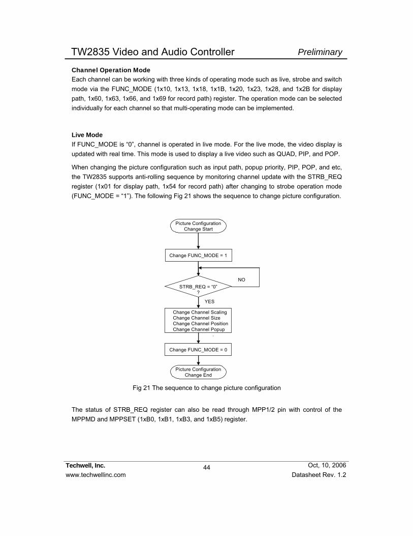
44
Techwell, Inc. www.techwellinc.com Datasheet Rev. 1.2
PreliminaryTW2835 Video and Audio Controller
Oct, 10, 2006
Channel Operation Mode Each channel can be working with three kinds of operating mode such as live, strobe and switch mode via the FUNC_MODE (1x10, 1x13, 1x18, 1x1B, 1x20, 1x23, 1x28, and 1x2B for display path, 1x60, 1x63, 1x66, and 1x69 for record path) register. The operation mode can be selected individually for each channel so that multi-operating mode can be implemented.
Live Mode If FUNC_MODE is “0”, channel is operated in live mode. For the live mode, the video display is updated with real time. This mode is used to display a live video such as QUAD, PIP, and POP.
When changing the picture configuration such as input path, popup priority, PIP, POP, and etc, the TW2835 supports anti-rolling sequence by monitoring channel update with the STRB_REQ register (1x01 for display path, 1x54 for record path) after changing to strobe operation mode (FUNC_MODE = “1”). The following Fig 21 shows the sequence to change picture configuration.
Change Channel ScalingChange Channel SizeChange Channel PositionChange Channel Popup
STRB_REQ = “0”?
YES
NO
Picture ConfigurationChange Start
Picture ConfigurationChange End
Change FUNC_MODE = 1
Change FUNC_MODE = 0
Fig 21 The sequence to change picture configuration
The status of STRB_REQ register can also be read through MPP1/2 pin with control of the MPPMD and MPPSET (1xB0, 1xB1, 1xB3, and 1xB5) register.

45
Techwell, Inc. www.techwellinc.com Datasheet Rev. 1.2
PreliminaryTW2835 Video and Audio Controller
Oct, 10, 2006
Strobe Mode If FUNC_MODE is “1”, channel is operated in strobe mode. For strobe mode, video display is updated whenever the TW2835 receives strobe command from host like CPU or Micom. If host doesn’t send a strobe command to the TW2835 anymore, the channel maintains the last strobe image until getting a new strobe command. This mode is useful to display non-realtime video input such as playback video with multiplexed signal input and to implement pseudo 8 channel application or dual page mode or panorama channel display. Specially, the TW2835 supports easy interface for pseudo 8channel application that will be covered in display path control section. The TW2835 also supports auto strobe function for auto playback display that will be covered later in auto strobe function section.
Strobe operation is performed independently for each channel via the STRB_REQ (1x04, 1x54) register. But the STRB_REQ register has a different mode for reading and writing. Writing “1” into STRB_REQ in each channel makes the TW2835 updated by each incoming video. The updating status after strobe command can be known by reading the STRB_REQ register. If reading value is “1”, updating is not completed after getting the strobe command. In that case, this channel cannot accept a new strobe command or a disabling strobe command from host. To send a new strobe command, host should wait until STRB_REQ state is “0”. For freeze or non-strobe channel, the TW2835 can ignore the strobe command even though host sends it. In this case, the STRB_REQ register is cleared to “0” automatically without any updating video. The status of STRB_REQ register can also be read through MPP1/2 pin with control of the MPPSET (1xB3) register.
When updating video with a strobe command, the TW2835 supports field or frame updating mode via the STRB_FLD (1x04, 1x54) register. Odd field of input video can be updated and displayed for STRB_FLD = “0”, even field for “1”. For “2” of STRB_FLD register, the TW2835 doesn’t care for even or odd field, and updates video by next any field. If the STRB_FLD register is “3”, the strobe command updates video by frame. The following Fig 22 shows the example of strobe sequence for various STRB_FLD value.
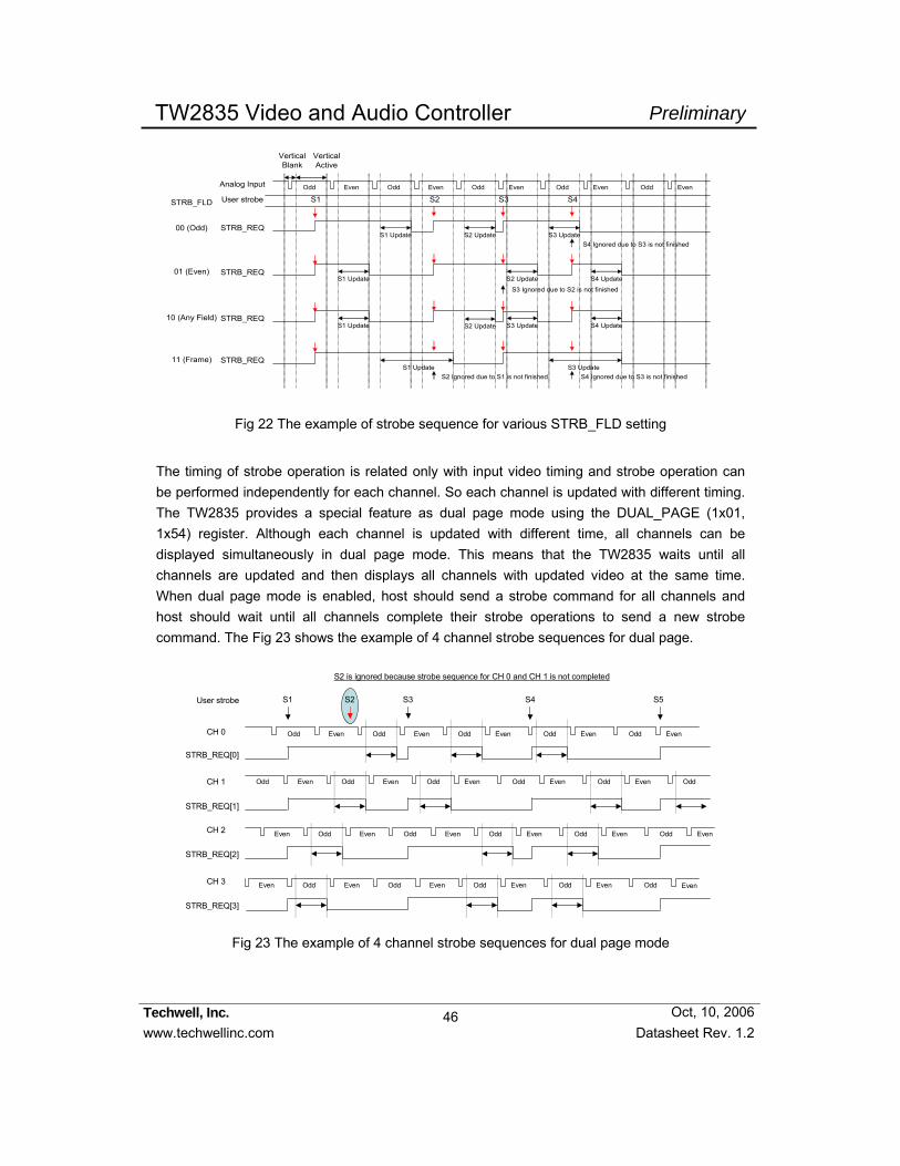
46
Techwell, Inc. www.techwellinc.com Datasheet Rev. 1.2
PreliminaryTW2835 Video and Audio Controller
Oct, 10, 2006
Analog Input
STRB_REQ
Vertical Blank
Vertical Active
S1 Update
S1 S3User strobe S2Odd Odd Odd OddEven Even Even Even Odd Even
S2 Update S3 Update
STRB_REQS1 Update S2 Update S4 Update
S1 UpdateSTRB_REQ
S4 UpdateS2 Update
STRB_REQS1 Update
S2 Ignored due to S1 is not finishedS3 Update
STRB_FLD
00 (Odd)
01 (Even)
10 (Any Field)
11 (Frame)
S4
S4 Ignored due to S3 is not finished
S3 Update
S3 Ignored due to S2 is not finished
S4 Ignored due to S3 is not finished
Fig 22 The example of strobe sequence for various STRB_FLD setting
The timing of strobe operation is related only with input video timing and strobe operation can be performed independently for each channel. So each channel is updated with different timing. The TW2835 provides a special feature as dual page mode using the DUAL_PAGE (1x01, 1x54) register. Although each channel is updated with different time, all channels can be displayed simultaneously in dual page mode. This means that the TW2835 waits until all channels are updated and then displays all channels with updated video at the same time. When dual page mode is enabled, host should send a strobe command for all channels and host should wait until all channels complete their strobe operations to send a new strobe command. The Fig 23 shows the example of 4 channel strobe sequences for dual page.
CH 0
STRB_REQ[0]
S4User strobe S3
Odd Odd Odd OddEven Even Even Even Odd Even
Odd Odd Odd OddEven Even Even Even Odd Even OddCH 1
STRB_REQ[1]
CH 2
STRB_REQ[2]
CH 3
STRB_REQ[3]
Odd Odd OddEven Even Even Odd EvenOdd EvenEven
Odd Odd OddEven Even Even OddOdd EvenEven
S1
Even
S2 S5
S2 is ignored because strobe sequence for CH 0 and CH 1 is not completed
Fig 23 The example of 4 channel strobe sequences for dual page mode
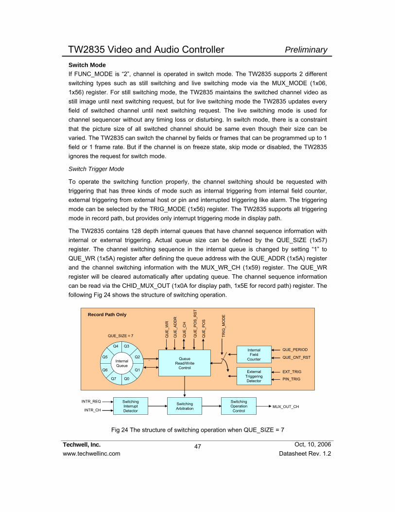
47
Techwell, Inc. www.techwellinc.com Datasheet Rev. 1.2
PreliminaryTW2835 Video and Audio Controller
Oct, 10, 2006
Switch Mode If FUNC_MODE is “2”, channel is operated in switch mode. The TW2835 supports 2 different switching types such as still switching and live switching mode via the MUX_MODE (1x06, 1x56) register. For still switching mode, the TW2835 maintains the switched channel video as still image until next switching request, but for live switching mode the TW2835 updates every field of switched channel until next switching request. The live switching mode is used for channel sequencer without any timing loss or disturbing. In switch mode, there is a constraint that the picture size of all switched channel should be same even though their size can be varied. The TW2835 can switch the channel by fields or frames that can be programmed up to 1 field or 1 frame rate. But if the channel is on freeze state, skip mode or disabled, the TW2835 ignores the request for switch mode.
Switch Trigger Mode
To operate the switching function properly, the channel switching should be requested with triggering that has three kinds of mode such as internal triggering from internal field counter, external triggering from external host or pin and interrupted triggering like alarm. The triggering mode can be selected by the TRIG_MODE (1x56) register. The TW2835 supports all triggering mode in record path, but provides only interrupt triggering mode in display path.
The TW2835 contains 128 depth internal queues that have channel sequence information with internal or external triggering. Actual queue size can be defined by the QUE_SIZE (1x57) register. The channel switching sequence in the internal queue is changed by setting “1” to QUE_WR (1x5A) register after defining the queue address with the QUE_ADDR (1x5A) register and the channel switching information with the MUX_WR_CH (1x59) register. The QUE_WR register will be cleared automatically after updating queue. The channel sequence information can be read via the CHID_MUX_OUT (1x0A for display path, 1x5E for record path) register. The following Fig 24 shows the structure of switching operation.
InternalQueue
Q3
Q2
Q1
Q0Q7
Q6
Q5
Q4
QueueRead/Write
Control
QUE_SIZE = 7
QUE_PERIOD
SwitchingArbitration
SwitchingInterruptDetector
InternalField
Counter QUE_CNT_RST
ExternalTriggeringDetector
EXT_TRIG
TRIG
_MO
DE
SwitchingOperation
Control
INTR_REQ
INTR_CHMUX_OUT_CH
QU
E_A
DD
R
QU
E_C
H
QU
E_P
OS
_RS
T
QU
E_P
OS
PIN_TRIG
Record Path Only
QU
E_W
R
Fig 24 The structure of switching operation when QUE_SIZE = 7
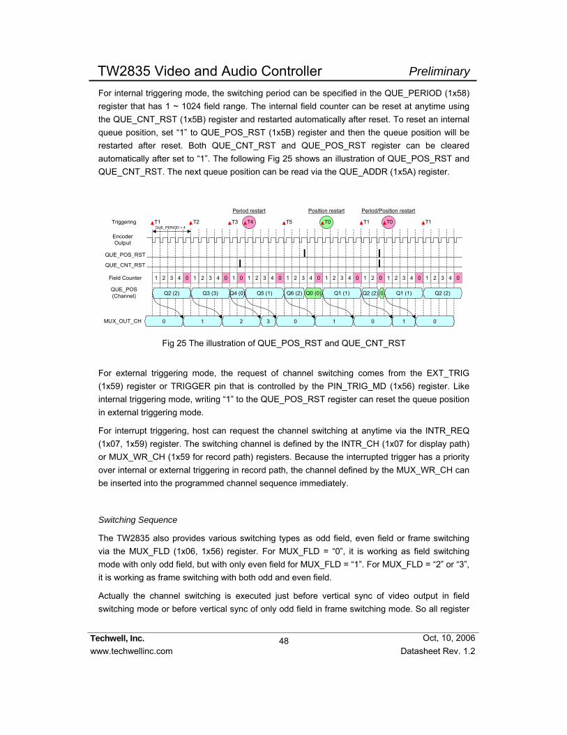
48
Techwell, Inc. www.techwellinc.com Datasheet Rev. 1.2
PreliminaryTW2835 Video and Audio Controller
Oct, 10, 2006
For internal triggering mode, the switching period can be specified in the QUE_PERIOD (1x58) register that has 1 ~ 1024 field range. The internal field counter can be reset at anytime using the QUE_CNT_RST (1x5B) register and restarted automatically after reset. To reset an internal queue position, set “1” to QUE_POS_RST (1x5B) register and then the queue position will be restarted after reset. Both QUE_CNT_RST and QUE_POS_RST register can be cleared automatically after set to “1”. The following Fig 25 shows an illustration of QUE_POS_RST and QUE_CNT_RST. The next queue position can be read via the QUE_ADDR (1x5A) register.
Q2 (2) Q4 (0)Q3 (3) Q5 (1) Q6 (2) Q1 (1) Q2 (2) Q2 (2)
1 32 0 1 0 1 00
Encoder Output
Triggering
QUE_POS (Channel)
MUX_OUT_CH
QUE_POS_RST
QUE_CNT_RST
QUE_PERIOD = 4
Q0 (0)
T1 T2 T3 T4 T5 T0
Period restart Period/Position restart
T0
Position restart
T1
0 Q1 (1)
T1
Field Counter 1 2 13 2 34 4 0 1 0 1 2 3 4 0 1 2 3 4 0 1 2 3 4 0 1 2 0 1 2 3 4 0 1 2 3 4 00
Fig 25 The illustration of QUE_POS_RST and QUE_CNT_RST
For external triggering mode, the request of channel switching comes from the EXT_TRIG (1x59) register or TRIGGER pin that is controlled by the PIN_TRIG_MD (1x56) register. Like internal triggering mode, writing “1” to the QUE_POS_RST register can reset the queue position in external triggering mode.
For interrupt triggering, host can request the channel switching at anytime via the INTR_REQ (1x07, 1x59) register. The switching channel is defined by the INTR_CH (1x07 for display path) or MUX_WR_CH (1x59 for record path) registers. Because the interrupted trigger has a priority over internal or external triggering in record path, the channel defined by the MUX_WR_CH can be inserted into the programmed channel sequence immediately.
Switching Sequence
The TW2835 also provides various switching types as odd field, even field or frame switching via the MUX_FLD (1x06, 1x56) register. For MUX_FLD = “0”, it is working as field switching mode with only odd field, but with only even field for MUX_FLD = “1”. For MUX_FLD = “2” or “3”, it is working as frame switching with both odd and even field.
Actually the channel switching is executed just before vertical sync of video output in field switching mode or before vertical sync of only odd field in frame switching mode. So all register

49
Techwell, Inc. www.techwellinc.com Datasheet Rev. 1.2
PreliminaryTW2835 Video and Audio Controller
Oct, 10, 2006
for switching should be set before that time. Otherwise, the control values will be applied to the next field or frame. Likewise, the switching channel information is updated just before vertical sync of video output in field switching or before vertical sync of only odd field in frame switching mode.
Basically the switching sequence takes 4 field duration to display the switching channel from any triggering (field or frame). The host can read the current switching channel information through the MUX_OUT_CH (1x08, 1x6E) register. The TW2835 also supports external pin output for this channel information with DLINKI and MPP1/2 pin via the MPP_MD and MPP_SET (1xB0, 1xB1, 1xB3, and 1xB5) register. The switching channel information can also be discriminated by the channel ID in the video stream. The following Fig 26 shows the illustration of channel switching with internal triggering.
LINK Pin
INTR_REQ
Vertical Blank
Vertical Active
T0Triggering T2
QUE_POS
Video output
T3
MUX_OUT_CH
Mux output delay = 4 Fields
3
T0 T1 T2
2103
032 03
T1
21
21
Encoder Output
Fig 26 The illustration of switching sequence when QUE_SIZE = 3, QUE_PERIOD = 1

50
Techwell, Inc. www.techwellinc.com Datasheet Rev. 1.2
PreliminaryTW2835 Video and Audio Controller
Oct, 10, 2006
The following Fig 27 shows the illustration of channel switching with the combination of internal triggering and interrupted triggering mode.
INTR_REQVertical Blank
Vertical Active
T0Triggering I3 T2
QUE_POS
T3
MUX_OUT_CH
Interrupt Output
Mux output delay = 4 Fields
Triggering is delayed due to switch interrupt
3
T0 T1 T2
1 21032
13032 0
I1
switch interrupt is inserted between programmed triggering
Interrupt Output
12 3
T1
Switch interrupt
Encoder output
Fig 27 The interrupted switching sequence when QUE_SIZE = 3, QUE_PERIOD = 1
The TW2835 supports the skip function of the switching queue for switch mode in record path. In single chip application, the auto skip function of the switching queue can be supported if the MUX_SKIP_EN (1x5B) register is “1” and the NOVID_MODE is “1” or “3”. But in the chip-to-chip cascaded application, the skip function should be forced with the MUX_SKIP_CH (1x5C, 1x5D) register because the switching queue for whole channels is located in the lowest slaver device but cannot get the no-video information from the other chips. The QUAD MUX function in chip-to-chip cascade application will be covered in the “Chip-to-Chip Cascade Operation (page 76)”.
51
Techwell, Inc. www.techwellinc.com Datasheet Rev. 1.2
PreliminaryTW2835 Video and Audio Controller
Oct, 10, 2006
Channel Attribute The TW2835 provides various channel attributes such as channel enabling, popup enabling, boundary selection, blank enabling, freeze, horizontal/vertical mirroring for both display and record path. As special feature, the TW2835 supports the last image capture function, save and recall function, image enhancement and playback input selection for display path. For last image capture mode, channel can be blanked or boundary can be blinked automatically on video loss state.
Background Control Summation of all active channel regions can be called as active region and the rest region except active region is defined as background region. The TW2835 supports background overlay and the overlay color is controlled via the BGDCOL (1x0F, 1x5F) register.
Boundary Control The TW2835 can overlay channel boundary on each channel region using the BOUND (1x11, 1x14, 1x19, 1x1C, 1x21, 1x24, 1x29, and 1x2C for display path, 1x61, 1x64, 1x67, and 1x6A for record path) register and it can be blinked via the BLINK (1x11, 1x14, 1x19, 1x1C, 1x21, 1x24, 1x29, and 1x2C for display path, 1x61, 1x64, 1x67, and 1x6A for record path) register when BOUND is high. The boundary color of channel can be selected through the BNDCOL (1x0F, 1x5F) register. The blink period can be also controlled through the TBLINK (1x01, 1x52) register.
Blank Control Each channel can be blanked with specified color using the BLANK (1x11, 1x14, 1x19, 1x1C, 1x21, 1x24, 1x29, and 1x2C for display path, 1x61, 1x64, 1x67, and 1x6A for record path) register and the blank color can be specified via the BLKCOL (1x0F, 1x3F) register.
Freeze Control Each channel can capture last 4 field images whenever freeze function is enabled and display 1 field image out of the captured 4 field images using the FRZ_FLD (1x0F, 1x3F) register. The freeze function can be enabled or disabled independently for each channel via the FREEZE (1x11, 1x14, 1x19, 1x1C, 1x21, 1x24, 1x29, and 1x2C for display path, 1x61, 1x64, 1x67, and 1x6A for record path) register. The TW2835 also supports frame freeze function via the FRZ_FRAME (1x01, 1x52) register, and 1 frame image out of the captured 2 frame images using the FRZ_FLD (1x0F, 1x3F) register.

52
Techwell, Inc. www.techwellinc.com Datasheet Rev. 1.2
PreliminaryTW2835 Video and Audio Controller
Oct, 10, 2006
Last Image Captured When video loss has occurred or gone, the TW2835 provides 4 kinds of indication such as bypass of incoming video, channel blank, capture of last image, and capture of last image with blinking channel boundary depending on the NOVID_MODE (1x05, 1x55) register. This function is working automatically on video loss. The capturing last image is same as freeze function described above. User can select 1 field image out of captured 4 filed images via the FRZ_FLD (1x0F, 1x5F) register which is shared with freeze function. The TW2835 has frame freeze function via the FRZ_FRAME (1x01, 1x52) register, and 1 frame image out of the captured 2 frame images using the FRZ_FLD (1x0F, 1x3F) register.
Horizontal / Vertical Mirroring The TW2835 supports image-mirroring function for horizontal and/or vertical direction. The horizontal mirroring is achieved via the H_MIRROR (1x11, 1x14, 1x19, 1x1C, 1x21, 1x24, 1x29, and 1x2C for display path, 1x61, 1x64, 1x67, and 1x6A for record path) register and the vertical mirroring is attained via the V_MIRROR (1x11, 1x14, 1x19, 1x1C, 1x21, 1x24, 1x29, and 1x2C for display path, 1x61, 1x64, 1x67, and 1x6A for record path) register. It is useful for a reflection image in the horizontal and vertical direction from dome camera or car-rear vision system.
Field to Frame Conversion If the displayed channel size is half size of the video input in vertical direction, the video input can be separated into two (odd/even) fields according to the line numbers such as odd line for odd field and even line for even field. With this conversion, the vertical resolution of the video input can be enhanced compared with simple half vertical scaling, but the field rate is reduced to half. This mode can be enabled via the FIELD_OP (1x12, 1x15, 1x1A, 1x1D, 1x22, 1x25, 1x2A, and 1x2D for display path, 1x62, 1x65, 1x68 and 1x6B for record path) register.

53
Techwell, Inc. www.techwellinc.com Datasheet Rev. 1.2
PreliminaryTW2835 Video and Audio Controller
Oct, 10, 2006
Display Path Control The TW2835 can save images in external memory and recall them to display. This function can be working in display path. The TW2835 also supports the special filter to enhance image quality in display path for non-realtime video display such as frozen image, recalled image from saved images or playback input with multiplexed video source. The TW2835 provides high performance 2X zoom function in the vertical and horizontal direction.
The TW2835 supports any kind of picture configuration for display path with arbitrary picture size, position and pop-up control. The TW2835 also provides 8 channel display function for full triplex application (Display + Record + Playback) and the pseudo 8ch display function for non-realtime application.
Save and Recall Function The save/recall function can be working independently for each channel and the number of the saved images depends on the picture size and field type. The TW2835 can save image only in live channel so that it cannot be saved in frozen channel. If channel is working on strobe operating mode, this channel can be saved with new strobe command. For switch operating mode, the channel can be saved only on switching time because this channel can be updated at this moment. But, the save function cannot be working simultaneously with 1 ~ 5 frame bitmap page mode because both regions are overlapped with each other.
To save image, several parameters should be controlled that are the SAVE_FLD, SAVE_HID, SAVE_ADDR (1x02) and SAVE_REQ (1x03) registers. The SAVE_FLD determines field or frame type for image to be saved. Even though the channel to be saved is hidden by upper layer picture, it can be saved using the SAVE_HID register that makes no effect on current display. The saving function is requested by writing “1” to the SAVE_REQ register and this register will be cleared when saving is done. Before it is cleared, the TW2835 cannot accept new saving request. The SAVE_ADDR register defines address where an image will be saved. Because 4M bits is allocated for each 1 field image, SAVE_ADDR can have range with 4 ~ 11 because the first 0~ 3 and last 12 ~ 15 addresses are reserved for normal operation so that it cannot be used for saving function.
To recall the saved video image, several parameters are required such as RECALL_FLD (1x03), RECALL_EN (1x11, 1x14, 1x19, 1x1C, 1x21, 1x24, 1x29, 1x2C) and RECALL_ADDR (1x12, 1x15, 1x1A, 1x1D, 1x22, 1x25, 1x2A, 1x2D) registers. If the RECALL_EN is “1”, the TW2835 recalls the saved image that is located at the RECALL_ADDR in external memory and displays it just like incoming video. The RECALL_FLD register determines 1 field or 1 frame mode to display.
The following Fig 28 illustrates the relationship between external SDRAM size and SAVE_ADDR / RECALL_ADDR.
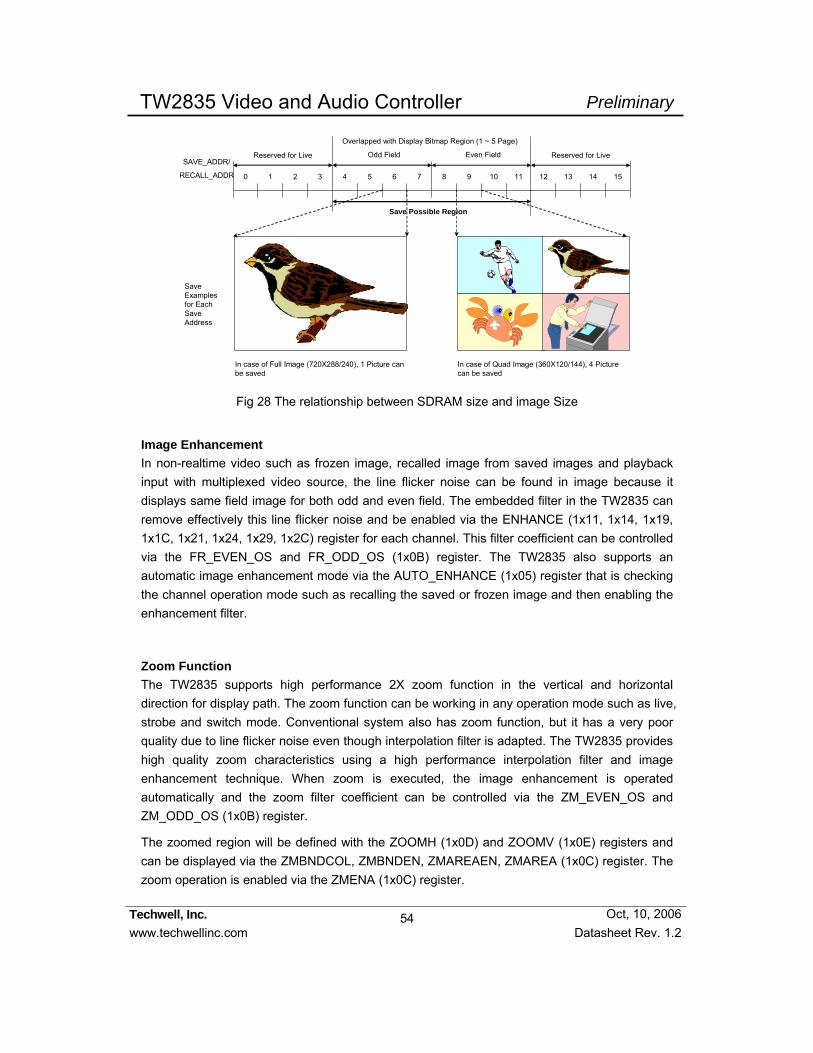
54
Techwell, Inc. www.techwellinc.com Datasheet Rev. 1.2
PreliminaryTW2835 Video and Audio Controller
Oct, 10, 2006
In case of Full Image (720X288/240), 1 Picture can be saved
In case of Quad Image (360X120/144), 4 Picture can be saved
Save Examples for Each Save Address
0
Reserved for Live
1 2 3 4 5 6 7 8 9 10 11 12 13 14 15
Reserved for Live
Save Possible Region
Overlapped with Display Bitmap Region (1 ~ 5 Page)
Odd Field Even FieldSAVE_ADDR/
RECALL_ADDR
Fig 28 The relationship between SDRAM size and image Size
Image Enhancement In non-realtime video such as frozen image, recalled image from saved images and playback input with multiplexed video source, the line flicker noise can be found in image because it displays same field image for both odd and even field. The embedded filter in the TW2835 can remove effectively this line flicker noise and be enabled via the ENHANCE (1x11, 1x14, 1x19, 1x1C, 1x21, 1x24, 1x29, 1x2C) register for each channel. This filter coefficient can be controlled via the FR_EVEN_OS and FR_ODD_OS (1x0B) register. The TW2835 also supports an automatic image enhancement mode via the AUTO_ENHANCE (1x05) register that is checking the channel operation mode such as recalling the saved or frozen image and then enabling the enhancement filter.
Zoom Function The TW2835 supports high performance 2X zoom function in the vertical and horizontal direction for display path. The zoom function can be working in any operation mode such as live, strobe and switch mode. Conventional system also has zoom function, but it has a very poor quality due to line flicker noise even though interpolation filter is adapted. The TW2835 provides high quality zoom characteristics using a high performance interpolation filter and image enhancement technique. When zoom is executed, the image enhancement is operated automatically and the zoom filter coefficient can be controlled via the ZM_EVEN_OS and ZM_ODD_OS (1x0B) register.
The zoomed region will be defined with the ZOOMH (1x0D) and ZOOMV (1x0E) registers and can be displayed via the ZMBNDCOL, ZMBNDEN, ZMAREAEN, ZMAREA (1x0C) register. The zoom operation is enabled via the ZMENA (1x0C) register.
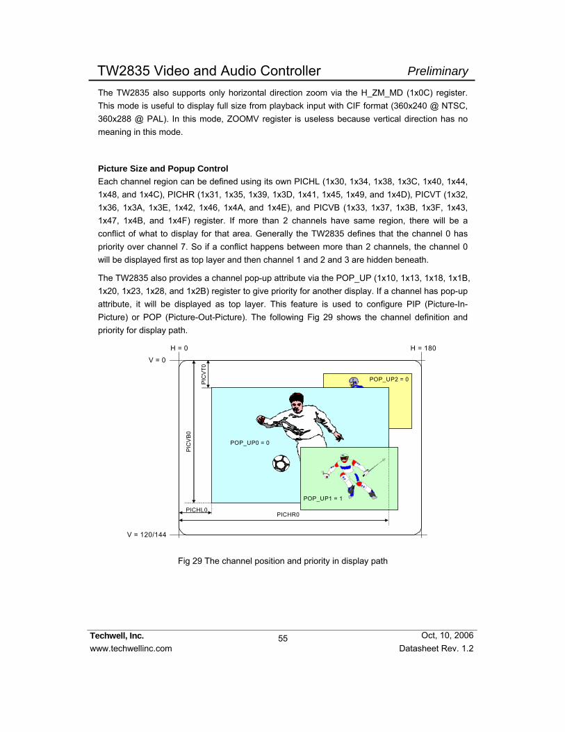
55
Techwell, Inc. www.techwellinc.com Datasheet Rev. 1.2
PreliminaryTW2835 Video and Audio Controller
Oct, 10, 2006
The TW2835 also supports only horizontal direction zoom via the H_ZM_MD (1x0C) register. This mode is useful to display full size from playback input with CIF format (360x240 @ NTSC, 360x288 @ PAL). In this mode, ZOOMV register is useless because vertical direction has no meaning in this mode.
Picture Size and Popup Control Each channel region can be defined using its own PICHL (1x30, 1x34, 1x38, 1x3C, 1x40, 1x44, 1x48, and 1x4C), PICHR (1x31, 1x35, 1x39, 1x3D, 1x41, 1x45, 1x49, and 1x4D), PICVT (1x32, 1x36, 1x3A, 1x3E, 1x42, 1x46, 1x4A, and 1x4E), and PICVB (1x33, 1x37, 1x3B, 1x3F, 1x43, 1x47, 1x4B, and 1x4F) register. If more than 2 channels have same region, there will be a conflict of what to display for that area. Generally the TW2835 defines that the channel 0 has priority over channel 7. So if a conflict happens between more than 2 channels, the channel 0 will be displayed first as top layer and then channel 1 and 2 and 3 are hidden beneath.
The TW2835 also provides a channel pop-up attribute via the POP_UP (1x10, 1x13, 1x18, 1x1B, 1x20, 1x23, 1x28, and 1x2B) register to give priority for another display. If a channel has pop-up attribute, it will be displayed as top layer. This feature is used to configure PIP (Picture-In-Picture) or POP (Picture-Out-Picture). The following Fig 29 shows the channel definition and priority for display path.
PIC
VT0
PIC
VB
0
PICHL0PICHR0
V = 0
H = 0
POP_UP0 = 0
POP_UP1 = 1
POP_UP2 = 0
H = 180
V = 120/144
Fig 29 The channel position and priority in display path
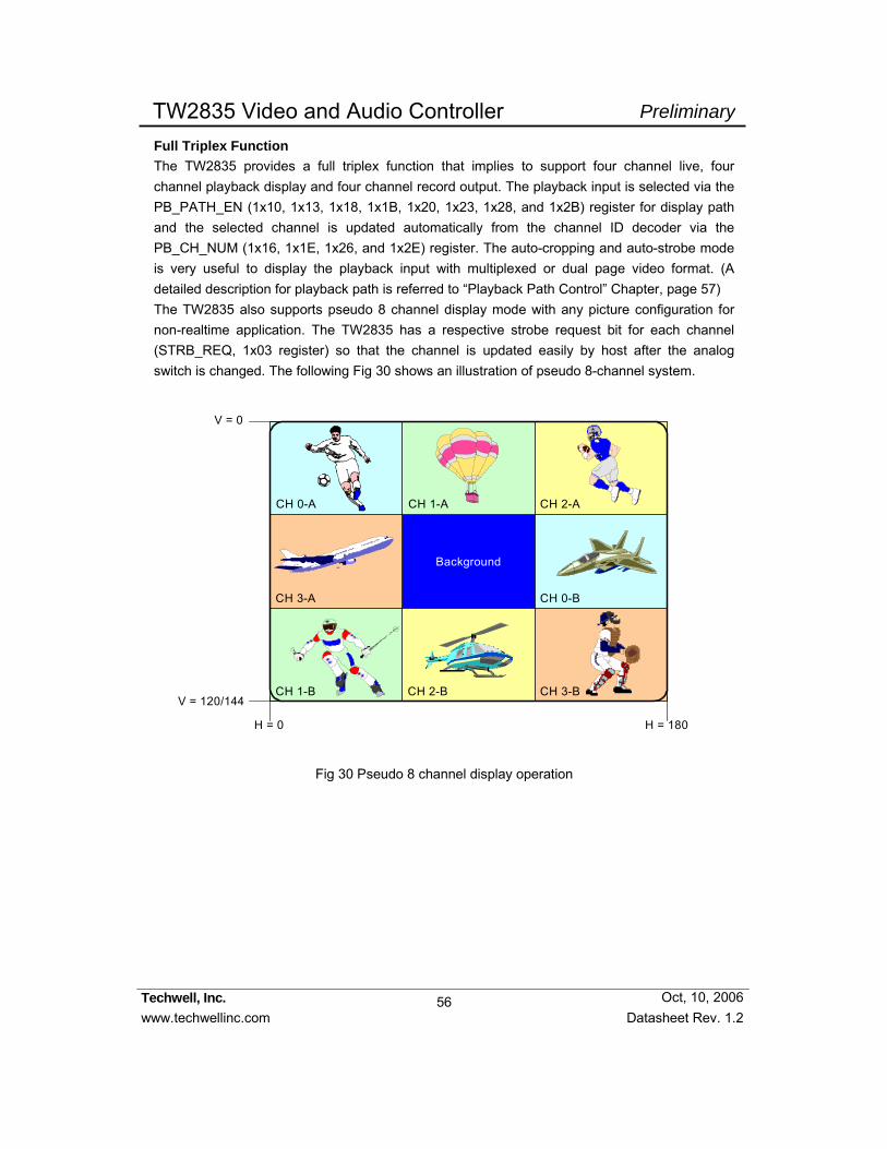
56
Techwell, Inc. www.techwellinc.com Datasheet Rev. 1.2
PreliminaryTW2835 Video and Audio Controller
Oct, 10, 2006
Full Triplex Function The TW2835 provides a full triplex function that implies to support four channel live, four channel playback display and four channel record output. The playback input is selected via the PB_PATH_EN (1x10, 1x13, 1x18, 1x1B, 1x20, 1x23, 1x28, and 1x2B) register for display path and the selected channel is updated automatically from the channel ID decoder via the PB_CH_NUM (1x16, 1x1E, 1x26, and 1x2E) register. The auto-cropping and auto-strobe mode is very useful to display the playback input with multiplexed or dual page video format. (A detailed description for playback path is referred to “Playback Path Control” Chapter, page 57) The TW2835 also supports pseudo 8 channel display mode with any picture configuration for non-realtime application. The TW2835 has a respective strobe request bit for each channel (STRB_REQ, 1x03 register) so that the channel is updated easily by host after the analog switch is changed. The following Fig 30 shows an illustration of pseudo 8-channel system.
Background
CH 0-A CH 1-A CH 2-A
CH 1-B CH 2-B CH 3-B
CH 3-A CH 0-B
V = 0
H = 0 H = 180
V = 120/144
Fig 30 Pseudo 8 channel display operation

57
Techwell, Inc. www.techwellinc.com Datasheet Rev. 1.2
PreliminaryTW2835 Video and Audio Controller
Oct, 10, 2006
Playback Path Control The TW2835 supports the playback function for variable record mode input such as normal record mode, frame record mode, DVR normal record mode, and DVR frame record mode. The TW2835 also provides auto cropping and auto strobe function for playback input through auto channel ID decoding. The auto strobe function implies that the selected channel is updated automatically from the playback input of the time-multiplexed full D1, CIF or Quad record format.
If the channel operation mode is live mode (FUNC_MODE = “0”), the playback input can be bypassed in display path, but the auto cropping function from the channel ID decoder is available to separate each channel from the multi-channel format such as QUAD (Auto cropping function is described in “Cropping Function” section, page 34). The displayed channel can be selected via the PB_CH_NUM (1x16, 1x1E, 1x26, and 1x2E) register.
If the channel operation mode is strobe mode (FUNC_MODE = “1”), the auto strobe function is used to update the channel automatically for the playback input of the time-multiplexed full D1, CIF or Quad record format through channel ID decoder. The auto strobe function is enabled by the PB_AUTO_EN (1x16) and PB_CH_NUM (1x16, 1x1E, 1x26, and 1x2E) register and can also be used for pseudo 8 channel display of playback input with the dual page mode or pseudo 8 channel MUX mode.
The TW2835 supports event strobe mode with event information in auto channel ID. It makes the channel updated whenever event information in auto channel ID is detected. The event strobe mode can be enabled via the EVENT_PB (1x16, 1x1E, 1x26, and 1x2E) register.
The TW2835 provides an anti-rolling function for the case of changing the picture configuration in playback application through the PB_STOP (1x16, 1x1E, 1x26, and 1x2E) register. If the PB_STOP is set to high in strobe operation mode (FUNC_MODE = “1”), the channel is not updated until the PB_STOP is set to low after picture configuration is changed.
To remove the image shaking from the playback input of frame switching mode, the TW2835 also supports frame to field conversion in auto strobe mode via the FLD_CONV (1x16, 1x1E, 1x26, and 1x2E) register. It makes the channel updated with only 1 field even though the playback input is made up of frame.

58
Techwell, Inc. www.techwellinc.com Datasheet Rev. 1.2
PreliminaryTW2835 Video and Audio Controller
Oct, 10, 2006
Normal Record Mode
The TW2835 provides various playback functions for normal record mode input. For playback input of live mode, the FUNC_MODE should be set to “0” and then it can be bypassed and displayed in live mode. For playback input of multiplexed record format, the FUNC_MODE should be set into “1” and then the auto strobe function is used for automatic display of the selected channel. . The following Fig 31 shows the examples of playback function for normal record mode using bypass, auto cropping, scaling, repositioning, and popup control.
CH0(Live)
CH1(Live)
CH2(Live)
CH3(Live)
CH0 CH1
CH2 CH3
1. Bypass (1Ch)
CH0
CH1 CH2
CH3
4. Crop + Reposition (4Ch)2. Bypass + Scaling (1Ch) 3. Bypass + Crop (1Ch)
CH3 CH1(Live)
CH2(Live)
CH3(Live)
CH1
CH2 CH3
CH1(Live)
CH2(Live)
CH3(Live)
CH0 CH1
CH2 CH3
5. Crop + Reposition + Scaling + Popup (5Ch)
CH0(Live)
CH1 CH2
CH3
Playback Input (QUAD) Display Path Output
CH0 CH1
CH2 CH3
6. Crop + Reposition + Scaling + Popup (8Ch)
CH0CH0
CH0
CH1 CH2
CH3
CH0(Live)
CH2(Live)
CH1(Live)CH3(Live)
7. Crop + Reposition + Scaling + Popup (8Ch)
CH0
CH1
CH2
CH3
CH1(Live)
CH0(Live)
CH3(Live)
CH2(Live)
8. Crop + Reposition + Scaling + Popup (8Ch)
Fig 31 The examples of the playback function for normal record mode
The following Fig 32 shows the various display examples for various playback input format using auto strobe function.
CH0(Live)
CH1(Live)
CH2(Live)
CH3(Live)
CH0(Live)
CH1(Live)
CH0 CH1
CH2 CH3
CH4 CH5
CH6 CH7
2. 16Ch Quad-MUX Crop + Strobe (1Ch)
CH0 CH1(Live)
CH2(Live)
CH3(Live)
Crop + Strobe (4Ch)
CH0
CH1 CH2
CH3
CH0 CH1
CH2 CH3
CH4 CH5
CH6 CH7
1. Dual Page Crop + Strobe (1Ch)
CH0 CH1(Live)
CH2(Live)
CH3(Live)
Crop + Strobe (4Ch)
CH0
CH1 CH2
CH3
Crop + Scale + Strobe (4Ch)
CH0
CH1 CH2 CH3
CH4
CH5 CH6 CH7
CH0
3. Switch mode
CH1
Crop + Scale + Strobe (4Ch)
CH0
CH1 CH2
CH3
Crop + Scale + Strobe (1Ch)
CH0
4. Pseudo-8Ch MUX
CH5
Crop + Scale + Strobe (4Ch)
CH0
CH1 CH2
CH3
CH0
Strobe (1Ch)
CH0
Strobe (1Ch) Crop + Strobe (1Ch)
CH2(Live)
CH3(Live)
CH0
Crop + Strobe (2Ch)
CH2(Live)
CH3(Live)
CH0 CH1
CH4
Scaling + Strobe (1Ch)
CH1(Live)
CH2(Live)
CH3(Live)
CH0 CH1
CH2 CH3
Scaling + Strobe (1Ch)
CH1(Live)
CH2(Live)
CH3(Live)
CH4 CH5
CH6 CH7
CH1 CH2 CH3
Crop + Strobe + scale (8Ch)
CH0
CH1 CH2 CH3
CH0
CH1 CH2
CH3
Scaling + Strobe (2Ch)
CH2(Live)
CH3(Live)
CH0 CH1
CH2 CH3
CH4 CH5
CH6 CH7CH0 CH1
CH2 CH3
Bypass (1Ch)
CH0 CH1
CH2 CH3
Bypass (1Ch)
Playback Input Display Path Output (Max 8 Ch Display in 1 Chip)
CH0 CH0
CH1 CH2 CH3
CH4
CH5 CH6 CH7
Crop + Strobe + scale (8Ch)
CH2(Live)
CH3(Live)
CH0
CH1 CH2 CH3
CH0
CH1 CH2 CH3
CH0
CH1 CH2 CH3
CH4
CH5 CH6 CH7
CH0
CH1 CH2 CH3
CH0
CH1 CH2 CH3
Crop + Scale + Strobe (4Ch)
CH0
CH1 CH2 CH3
Fig 32 The example of auto strobe function for normal record mode
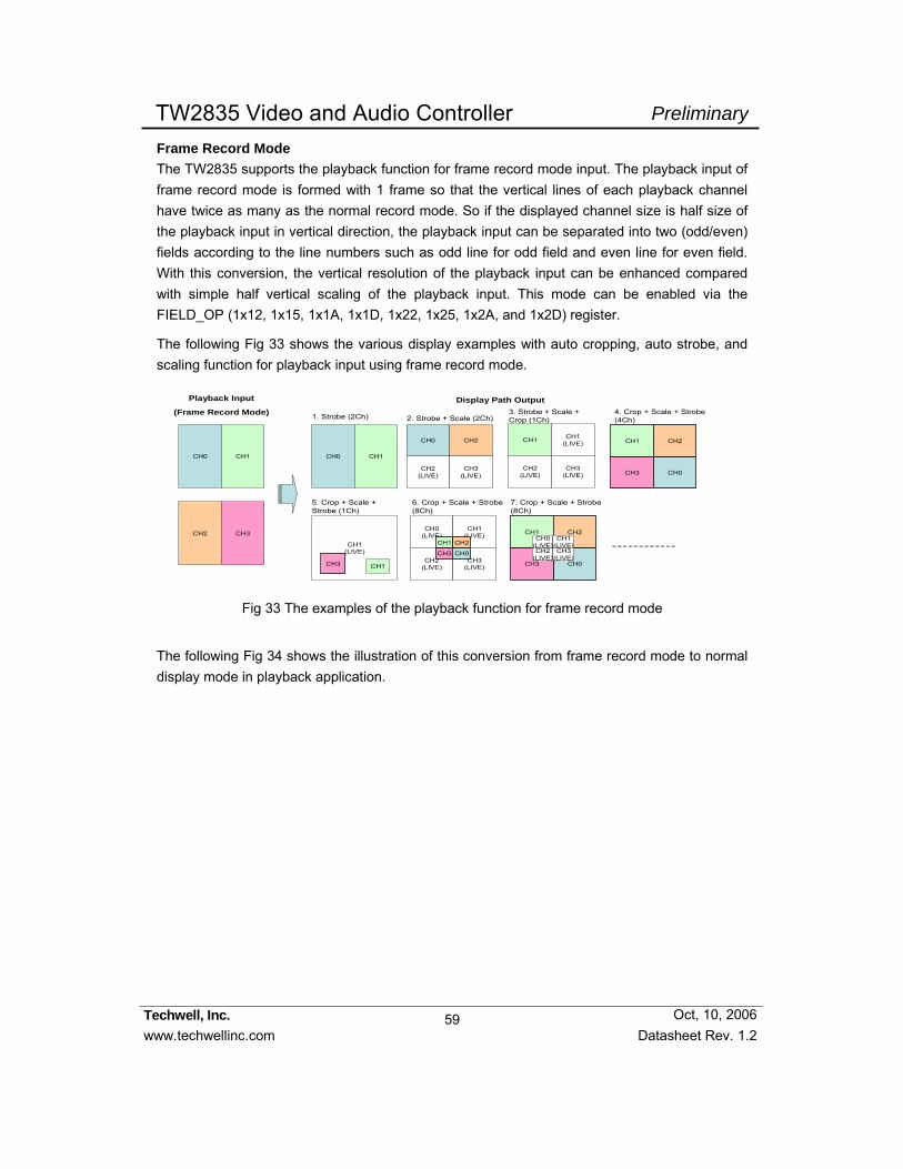
59
Techwell, Inc. www.techwellinc.com Datasheet Rev. 1.2
PreliminaryTW2835 Video and Audio Controller
Oct, 10, 2006
Frame Record Mode The TW2835 supports the playback function for frame record mode input. The playback input of frame record mode is formed with 1 frame so that the vertical lines of each playback channel have twice as many as the normal record mode. So if the displayed channel size is half size of the playback input in vertical direction, the playback input can be separated into two (odd/even) fields according to the line numbers such as odd line for odd field and even line for even field. With this conversion, the vertical resolution of the playback input can be enhanced compared with simple half vertical scaling of the playback input. This mode can be enabled via the FIELD_OP (1x12, 1x15, 1x1A, 1x1D, 1x22, 1x25, 1x2A, and 1x2D) register.
The following Fig 33 shows the various display examples with auto cropping, auto strobe, and scaling function for playback input using frame record mode.
CH0 CH1
CH2 CH3
4. Crop + Scale + Strobe (4Ch)
CH0
CH1 CH2
CH3
1. Strobe (2Ch)
Playback Input
(Frame Record Mode)Display Path Output
CH0 CH1
CH0 CH2
CH2(LIVE)
CH3(LIVE)
2. Strobe + Scale (2Ch)3. Strobe + Scale + Crop (1Ch)
CH1 CH1(LIVE)
CH2(LIVE)
CH3(LIVE)
CH1(LIVE)
CH1
5. Crop + Scale + Strobe (1Ch)
CH0(LIVE)
CH1(LIVE)
CH2(LIVE)
CH3(LIVE)
6. Crop + Scale + Strobe (8Ch)
CH0
CH1 CH2
CH3
7. Crop + Scale + Strobe (8Ch)
CH0
CH1 CH2
CH3
CH0(LIVE)
CH1(LIVE)
CH2(LIVE)
CH3(LIVE)
CH3
Fig 33 The examples of the playback function for frame record mode
The following Fig 34 shows the illustration of this conversion from frame record mode to normal display mode in playback application.

60
Techwell, Inc. www.techwellinc.com Datasheet Rev. 1.2
PreliminaryTW2835 Video and Audio Controller
Oct, 10, 2006
Normal Display Mode (Quad)
Input Video is Frame Quad (360 pixels X 240 Lines / Ch)Vertical is divided to 2Horizontal is divided to 2
Frame Record Mode (Frame-Quad)(Play back Input)
Output Video is divided to Odd/Even(360 pixels X 120 Lines / Ch * 2 Field) Odd Line Data go to Odd Field.Even Line Data go to Even Field.
Pixels Pixels
0
240/288
0 720360
Line
s
120/144
480/576
0
0 720360
Vertical Blanking (Even) Vertical Blanking (Even)
Vertical Blanking (Odd) Vertical Blanking (Odd)
CH 0
CH 2 CH 3
CH 1
CH0 (Odd Line)
CH0 (Even Line)
240/288
0
360/432
480/576
CH 0
CH 0
CH 3
CH 3
CH 3
CH 2 CH 1
CH 2 CH 1
Fig 34 The conversion from frame record mode to normal display mode
The TW2835 also supports only horizontal zoom mode via the H_ZM_MD (1x0C) register. This mode is useful to display the playback input of frame record mode to full size image. The following Fig 35 shows the illustration of this conversion in playback application.
Strobe Mode (2 Ch) +Enhance
Input Video is Frame Quad (360 pixels X 240 Lines / Ch)Vertical is divided to 2Horizontal is divided to 2
Frame Record Mode (Frame-Quad)(Play back Input)
Pixels
0
240/288
0 720360
Vertical Blanking (Even)
Vertical Blanking (Odd)
CH 0
CH 2 CH 3
CH 1
480/576
CH 1
Strobe Mode (2 Ch) +H Only Zoom + Enhance
Output Video is 1 Channel with Full Size (720 pixels X 480 Lines / Ch)
CH 2 CH 2
Output Video is 2 Channel with Half Size (360 pixels X 480 Lines / Ch)
360 720 7200 0
ZOOMH = 0
Fig 35 The conversion from frame record mode to full image
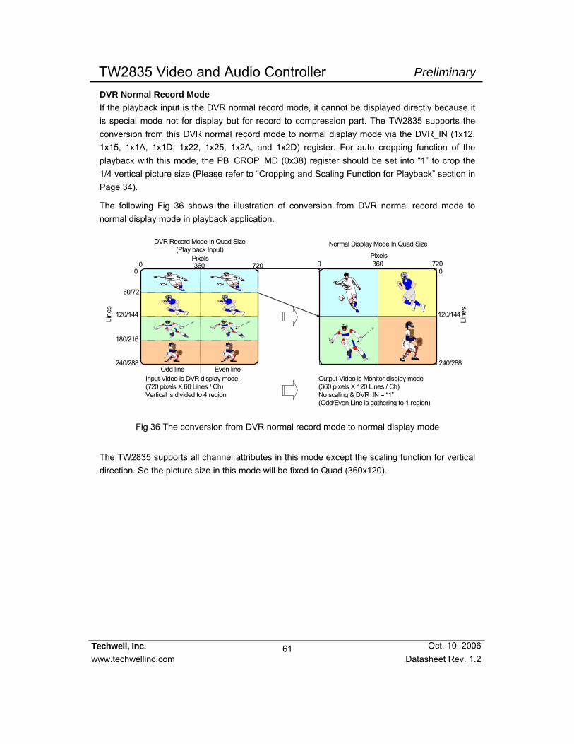
61
Techwell, Inc. www.techwellinc.com Datasheet Rev. 1.2
PreliminaryTW2835 Video and Audio Controller
Oct, 10, 2006
DVR Normal Record Mode If the playback input is the DVR normal record mode, it cannot be displayed directly because it is special mode not for display but for record to compression part. The TW2835 supports the conversion from this DVR normal record mode to normal display mode via the DVR_IN (1x12, 1x15, 1x1A, 1x1D, 1x22, 1x25, 1x2A, and 1x2D) register. For auto cropping function of the playback with this mode, the PB_CROP_MD (0x38) register should be set into “1” to crop the 1/4 vertical picture size (Please refer to “Cropping and Scaling Function for Playback” section in Page 34).
The following Fig 36 shows the illustration of conversion from DVR normal record mode to normal display mode in playback application.
0
240/288
120/144
Output Video is Monitor display mode(360 pixels X 120 Lines / Ch)No scaling & DVR_IN = “1”(Odd/Even Line is gathering to 1 region)
Normal Display Mode In Quad Size
0 720360Pixels
Line
s
DVR Record Mode In Quad Size(Play back Input)
Odd line Even lineInput Video is DVR display mode. (720 pixels X 60 Lines / Ch) Vertical is divided to 4 region
60/72
180/216
00 720360
Pixels
240/288
120/144
Line
s
Fig 36 The conversion from DVR normal record mode to normal display mode
The TW2835 supports all channel attributes in this mode except the scaling function for vertical direction. So the picture size in this mode will be fixed to Quad (360x120).

62
Techwell, Inc. www.techwellinc.com Datasheet Rev. 1.2
PreliminaryTW2835 Video and Audio Controller
Oct, 10, 2006
DVR Frame Record Mode The TW2835 also provides the conversion from DVR frame record mode to normal display mode using combination of frame record mode and DVR normal record mode via the DVR_IN and FIELD_OP (1x12, 1x15, 1x1A, 1x1D, 1x22, 1x25, 1x2A, and 1x2D) register. The following Fig 37 shows the illustration of conversion from DVR frame record mode to normal display mode in playback application.
Normal Display Mode (Quad)
Input Video is Frame Quad (720 pixels X 120 Lines / Ch)Vertical is divided to 4Horizontal is divided to 1
DVR Frame Record Mode (Frame-Quad)(Play back Input)
Output Video is divided to Odd/Even(360 pixels X 120 Lines / Ch * 2 Field) Left Half Line Data go to Odd Field.Right Half Line Data go to Even Field.
Pixels
120/144
240/288
0
0 720360Pixels
Vertical Blanking (Even)
Vertical Blanking (Odd)
Left Half Line
Right Half Line
240/288
0
120/144
CH 0
CH 0
CH 1
CH 2 CH 3
CH 1
CH 2 CH 3
120/144
480/576
0
0 720360
Vertical Blanking (Even)
Vertical Blanking (Odd)
240/288
360/432
Line
s
CH 0
CH 1
CH 2
CH 3
Fig 37 The conversion from DVR frame record mode to normal display mode
Like DVR normal record mode, all channel attributes can be supported, but the scaling function cannot be supported in this mode. So the channel size will be fixed to Quad size. To implement PIP or POP application with smaller size than Quad, only odd line data is used with channel size definition, scaling and enhancement function.
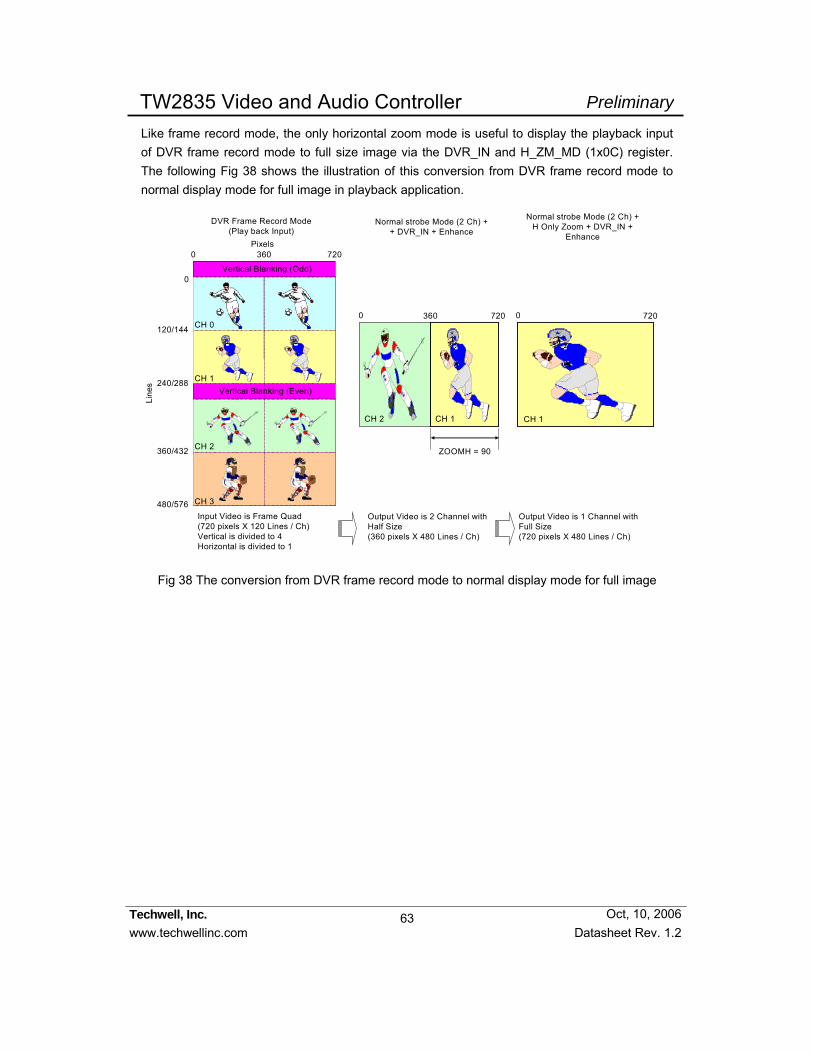
63
Techwell, Inc. www.techwellinc.com Datasheet Rev. 1.2
PreliminaryTW2835 Video and Audio Controller
Oct, 10, 2006
Like frame record mode, the only horizontal zoom mode is useful to display the playback input of DVR frame record mode to full size image via the DVR_IN and H_ZM_MD (1x0C) register. The following Fig 38 shows the illustration of this conversion from DVR frame record mode to normal display mode for full image in playback application.
Input Video is Frame Quad (720 pixels X 120 Lines / Ch)Vertical is divided to 4Horizontal is divided to 1
DVR Frame Record Mode(Play back Input)
Pixels
120/144
480/576
0
0 720360
Vertical Blanking (Even)
Vertical Blanking (Odd)
240/288
360/432
Line
s
CH 0
CH 1
CH 2
CH 3
Normal strobe Mode (2 Ch) ++ DVR_IN + Enhance
CH 1
Normal strobe Mode (2 Ch) +H Only Zoom + DVR_IN +
Enhance
Output Video is 1 Channel with Full Size (720 pixels X 480 Lines / Ch)
CH 2 CH 1
Output Video is 2 Channel with Half Size (360 pixels X 480 Lines / Ch)
360 720 7200 0
ZOOMH = 90
Fig 38 The conversion from DVR frame record mode to normal display mode for full image

64
Techwell, Inc. www.techwellinc.com Datasheet Rev. 1.2
PreliminaryTW2835 Video and Audio Controller
Oct, 10, 2006
Record Path Control The TW2835 supports 4 record modes such as normal record mode, frame record mode, DVR record mode and DVR frame record mode. The DVR record mode and DVR frame record mode generate continuous video stream for each channel and transfer it to compression part (M-JPEG or MPEG) so that they are very useful for DVR application. The frame record mode can be used to record each channel with full vertical resolution. Especially the TW2835 includes a noise reduction filter in record path so that it can reduce spot noise and then provide less compression file size.
The record mode is selected via the DIS_MODE and FRAME_OP (1x51) register. If the FRAME_OP is “0”, the DIS_MODE = “0” stands for normal record mode and the DIS_MODE = “1” represents DVR record mode. If the FRAME_OP is “1”, the DIS_MODE = “0” stands for frame record mode and the DIS_MODE = “1” represents DVR frame record mode.
The TW2835 supports high performance free scaler vertically and horizontally in display path, but has the size and position limitation such as Full / Quad / CIF in record path. The TW2835 also provides four channel real-time record mode with full D1 format using DLINKI and MPP1/2 pin.

65
Techwell, Inc. www.techwellinc.com Datasheet Rev. 1.2
PreliminaryTW2835 Video and Audio Controller
Oct, 10, 2006
Normal Record Mode Each channel position and size can be defined using its own PIC_SIZE (1x6C), and PIC_POS (1x6D) register. The channel size is defined via the PIC_SIZE register such as “0” for horizontal and vertical half size (QUAD), “1” for horizontal full size and vertical half size, “2” for horizontal half size and vertical full size, and “3” for horizontal and vertical full size. The channel position is defined via the PIC_POS register such as “0” for no horizontal and vertical offset, “1” for only horizontal half offset, “2” for only vertical half offset, and “3” for horizontal and vertical half offset. The channel size and location should be defined within the full picture size. (i.e. PIC_SIZE = “3” & PIC_POS = “2” is not allowed)
The horizontal full size of picture is controlled via the SIZE_MODE (1x51) register such as “0” for 720 pixels, “1” for 702 pixels, and “2” for 640 pixels. Likewise, the vertical full size is selected by the SYS5060 (1x00) register such as “0” for 240 lines and “1” for 288 lines.
If more than 2 channels have same region, there will be a conflict of what to display for that area. Generally the TW2835 defines that the channel 0 has priority over channel 3. So if a conflict happens between more than 2 channels, the channel 0 will be displayed first as top layer and then the channel 1, 2 and 3 are hidden beneath. The TW2835 also provides a channel pop-up attribute via the POP_UP (1x60, 1x63, 1x66, and 1x69) register to give priority for another display. If a channel has pop-up attribute, it will be displayed as top layer. The following Fig 39 shows the example of the channel position and size control in normal record mode.
Horizontal Direction (H)
PIC_SIZE = 0PIC_POS = 1
PIC_SIZE = 0PIC_POS = 3
PIC_SIZE = 0PIC_POS = 2Ve
rtica
l Dire
ctio
n (V
)
PIC_SIZE = 0PIC_POS = 0
CH 0 CH 1
CH 3CH 2
Fig 39 The channel position and size control in normal record mode

66
Techwell, Inc. www.techwellinc.com Datasheet Rev. 1.2
PreliminaryTW2835 Video and Audio Controller
Oct, 10, 2006
Frame Record Mode The frame record mode is similar to normal record mode except that the definition of picture size is extended to frame area and only one field data can be output in 1 frame. The odd or even field selection is controlled via the FRAME_FLD (1x51) register. Like normal record mode, each channel position and size are defined using its own PIC_SIZE (1x6C), and PIC_POS (1x6D) register. The channel size is defined via the PIC_SIZE register such as “0” for horizontal half size and vertical full size, “1” for horizontal and vertical full size, but “2” or “3” is not allowed. That is, the channel size for vertical direction supports only one field size. The channel position is defined via the PIC_POS register such as “0” for no horizontal and vertical offset, “1” for only horizontal half offset, “2” for only vertical 1 field offset, and “3” for horizontal half picture offset and vertical 1 field offset. The channel size and location should be defined within the full picture size. In frame record mode, the TW2835 also supports the full operation mode such as live, strobe or switch operation and provides a pop-up attribute via the POP_UP register. The Fig 40 shows the example of the channel position and size control in frame record mode.
F ra m e R e c o rd M o d e (F ra m e -Q u a d )(P IC _ S IZ E = 0 )
Out
put D
ata
of O
dd F
ield
Out
put D
ata
of E
ven
Fiel
d
V e r t ic a l B la n k in g
V e r t ic a l B la n k in g
N o rm a l R e c o r d M o d e (Q u a d )(P IC _ S IZ E = 0 )
0
Out
put D
ata
of O
dd F
ield
Out
put D
ata
of E
ven
Fiel
d
V e r t ic a l B la n k in g
V e r t ic a l B la n k in g
V id e o In p u t fo r E a c h C h a n n e lS c a le r a t io fo r H o r iz o n ta l : 1 /2S c a le r a t io fo r V e r t ic a l : 1 / 2
V id e o In p u t fo r E a c h C h a n n e lS c a le r a t io fo r H o r iz o n ta l : 1 /2S c a le r a t io fo r V e r t ic a l : 1
P IC _ P O S = 0
P IC _ P O S = 2 P IC _ P O S = 3
P IC _ P O S = 1
P IC _ P O S = 0 P IC _ P O S = 1
P IC _ P O S = 2 P IC _ P O S = 3
P IC _ P O S = 0
P IC _ P O S = 2 P IC _ P O S = 3
P IC _ P O S = 1
0
2 4 0 /2 8 8
4 8 0 /5 7 6
2 4 0 /2 8 8
4 8 0 /5 7 6
Fig 40 The channel position and size control in frame record mode
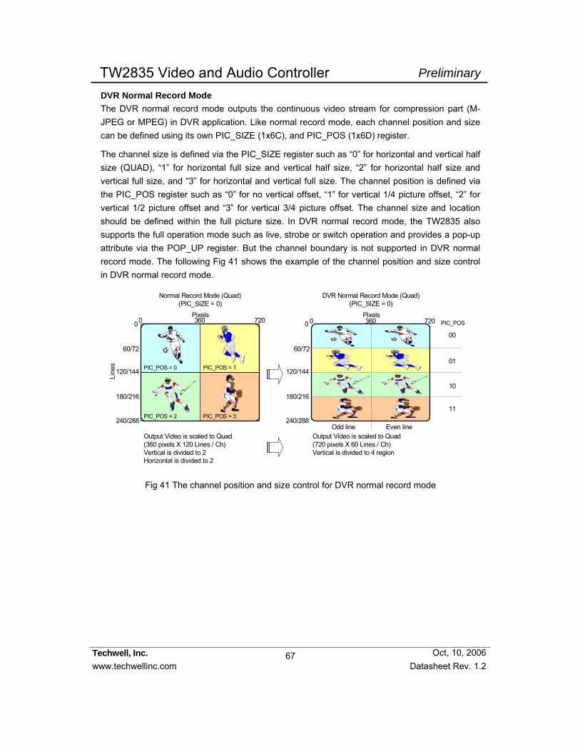
67
Techwell, Inc. www.techwellinc.com Datasheet Rev. 1.2
PreliminaryTW2835 Video and Audio Controller
Oct, 10, 2006
DVR Normal Record Mode The DVR normal record mode outputs the continuous video stream for compression part (M-JPEG or MPEG) in DVR application. Like normal record mode, each channel position and size can be defined using its own PIC_SIZE (1x6C), and PIC_POS (1x6D) register.
The channel size is defined via the PIC_SIZE register such as “0” for horizontal and vertical half size (QUAD), “1” for horizontal full size and vertical half size, “2” for horizontal half size and vertical full size, and “3” for horizontal and vertical full size. The channel position is defined via the PIC_POS register such as “0” for no vertical offset, “1” for vertical 1/4 picture offset, “2” for vertical 1/2 picture offset and “3” for vertical 3/4 picture offset. The channel size and location should be defined within the full picture size. In DVR normal record mode, the TW2835 also supports the full operation mode such as live, strobe or switch operation and provides a pop-up attribute via the POP_UP register. But the channel boundary is not supported in DVR normal record mode. The following Fig 41 shows the example of the channel position and size control in DVR normal record mode.
0
240/288
60/72
120/144
180/216
DVR Normal Record Mode (Quad)(PIC_SIZE = 0)
PIC_POS
00
01
10
11
Output Video is scaled to Quad (360 pixels X 120 Lines / Ch)Vertical is divided to 2Horizontal is divided to 2
Odd line Even line
Normal Record Mode (Quad)(PIC_SIZE = 0)
0 720360
Output Video is scaled to Quad (720 pixels X 60 Lines / Ch) Vertical is divided to 4 region
Pixels
Line
s
60/72
180/216
0 0 720360Pixels
PIC_POS = 0
PIC_POS = 2
PIC_POS = 1
PIC_POS = 3240/288
120/144
Fig 41 The channel position and size control for DVR normal record mode

68
Techwell, Inc. www.techwellinc.com Datasheet Rev. 1.2
PreliminaryTW2835 Video and Audio Controller
Oct, 10, 2006
DVR Frame Record Mode The DVR frame record mode is the combination of frame record mode and DVR normal record mode. The odd or even field selection is controlled via the FRAME_FLD (1x51) register like frame record mode. The TW2835 also supports the full operation mode such as live, strobe or switch operation, but the channel boundary is not supported in DVR frame record mode.
Like frame record mode, each channel position and size can be defined using its own PIC_SIZE (1x6C), and PIC_POS (1x6D) register. The channel size is defined via the PIC_SIZE register such as “0” for horizontal half size and vertical full size, “1” for horizontal and vertical full size, but “2” or “3” is not allowed. The channel position is defined via the PIC_POS register such as “0” for no horizontal and vertical offset, “1” for vertical half offset, “2” for vertical 1 field offset, and “3” for vertical 1 and half field offset. The channel size and location should be defined within the full picture size. The following Fig 42 shows the example of DVR frame record mode.
0
240/288
DVR Frame Record Mode (Frame-Quad)(PIC_SIZE = 0)
Output Video is scaled to Frame Quad (360 pixels X 240 Lines / Ch)Vertical is divided to 2Horizontal is divided to 2
Odd line Even line
Frame Record Mode (Frame-Quad)(PIC_SIZE = 0)
0 720360
Output Video is scaled to Frame Quad (720 pixels X 120 Lines / Ch) Vertical is divided to 4Horizontal is divided to 1
Pixels
Line
s
120/144
480/576
0
0 720360Pixels
Vertical Blanking (Even) Vertical Blanking (Even)
Vertical Blanking (Odd) Vertical Blanking (Odd)
PIC_POS = 0
PIC_POS = 2 PIC_POS = 3
PIC_POS = 1
PIC_POS = 0
PIC_POS = 1
PIC_POS = 2
PIC_POS = 3
240/288
360/432
480/576
Fig 42 The channel position and size control for DVR frame record mode

69
Techwell, Inc. www.techwellinc.com Datasheet Rev. 1.2
PreliminaryTW2835 Video and Audio Controller
Oct, 10, 2006
Noise Reduction The TW2835 includes a noise reduction filter in record path and the characteristic can be controlled via the TM_WIN_MD (1x53), MEDIAN_MD, TM_SLOP, and TM_THR (1x50) register. But this noise reduction filter is only available for normal record mode.
The TM_WIN_MD register defines window type to reduce spot noise as “0” for 3X3 matrix, “1” for cross matrix, “2” for multiplier matrix, and “3” for vertical bar matrix. The MEDIAN_MD defines the noise reduction filter mode as “0” for adaptive threshold median filter mode, “1” for normal median filter mode. For adaptive threshold median filter mode, the TW2835 has cross-correlation detector for noise detection. If cross-correlation value is over than TM_THR of noise threshold level, the noise reduction filter will be operated according to the graph defined by the TM_SLOP register.
The following Fig 43 shows the slope control for adaptive threshold median filter mode.
Y(i,j) = TM[x(i,j)] = (1- β) x(i,j) + β M(i,j)
β
TM_THR Cross-corelation
1
0
TM_SLOP = 0
TM_SLOP = 1
TM_SLOP = 2
TM_SLOP = 3
Fig 43 The slope control for adaptive threshold median filter mode
The TW2835 supports the noise reduction filter for each channel via the NR_EN (1x60, 1x63, 1x66, and 1x69) register. The TW2835 also supports auto noise reduction filter mode via the AUTO_NR_EN (1x55) register that is enabled when night is detected. Additionally the TW2835 has programmable black level of luminance component in record path to reduce the black spot noise via the LIM_656_Y (0xC1, and 0xC2) register.
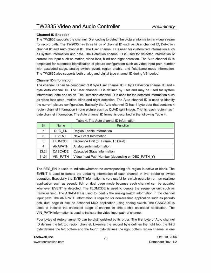
70
Techwell, Inc. www.techwellinc.com Datasheet Rev. 1.2
PreliminaryTW2835 Video and Audio Controller
Oct, 10, 2006
Channel ID Encoder The TW2835 supports the channel ID encoding to detect the picture information in video stream for record path. The TW2835 has three kinds of channel ID such as User channel ID, Detection channel ID and Auto channel ID. The User channel ID is used for customized information such as system information and date. The Detection channel ID is used for detected information of current live input such as motion, video loss, blind and night detection. The Auto channel ID is employed for automatic identification of picture configuration such as video input path number with cascaded stage, analog switch, event, region enable, and field/frame mode information. The TW2835 also supports both analog and digital type channel ID during VBI period.
Channel ID Information The channel ID can be composed of 8 byte User channel ID, 8 byte Detection channel ID and 4 byte Auto channel ID. The User channel ID is defined by user and may be used for system information, date and so on. The Detection channel ID is used for the detected information such as video loss state, motion, blind and night detection. The Auto channel ID is used to identify the current picture configuration. Basically the Auto channel ID has 4 byte data that contains 4 region channel information in one picture such as QUAD split image. That is, each region has 1 byte channel information. The Auto channel ID format is described in the following Table 4.
Table 4. The Auto channel ID information Bit Name Function
7 REG_EN Region Enable Information 6 EVENT New Event Information 5 FLDMODE Sequence Unit (0 : Frame, 1 : Field) 4 ANAPATH Analog switch information
[3:2] CASCADE Cascaded Stage Information [1:0] VIN_PATH Video Input Path Number (depending on DEC_PATH_Y)
The REG_EN is used to indicate whether the corresponding 1/4 region is active or blank. The EVENT is used to denote the updating information of each channel in live, strobe or switch operation. Especially the EVENT information is very useful for switch operation or non-realtime application such as pseudo 8ch or dual page mode because each channel can be updated whenever EVENT is detected. The FLDMODE is used to denote the sequence unit such as frame or field. The ANAPATH is used to identify the analog switch information in the channel input path. The ANAPATH information is required for non-realtime application such as pseudo 8ch, dual page or pseudo 8channel MUX application using analog switch. The CASCADE is used to indicate the cascaded stage of channel in chip-to-chip cascaded application. The VIN_PATH information is used to indicate the video input path of channel.
Four bytes of Auto channel ID can be distinguished by its order. The first byte of Auto channel ID defines the left top region channel. Likewise the second byte defines the right top, the third byte defines the left bottom and the fourth byte defines the right bottom region channel in one

71
Techwell, Inc. www.techwellinc.com Datasheet Rev. 1.2
PreliminaryTW2835 Video and Audio Controller
Oct, 10, 2006
picture. The following Fig 44 shows the example of Auto channel ID for various recording output formats.
CH0
CH3
CH2
CH1
CH0
CH1
CH2
CH3
CH0
CH0
CH3CH2
CH1CH0
CH3CH2
CH1 A0 = “1100_0000
A1 = “1100_0001
A2 = “1100_0010
A3 = “1100_0011
A0 = “1110_0001
A1 = “1110_0010
A2 = “1110_0001
A3 = “1110_0010
CH2CH1
Normal (QUAD Frame) Frame (Odd Field)
Frame (Even Field)
Auto Channel ID Auto Channel ID
Auto Channel ID
CH3CH0
A0 = “1110_0000
A1 = “1110_0011
A2 = “1110_0000
A3 = “1110_0011
CH0
Normal (Full Frame)
A0 = “1100_0000
A1 = “1100_0000
A2 = “1100_0000
A3 = “1100_0000
Auto Channel ID
CH0CH3
Full Field (Ch 0)Full Field (Ch 3)
A0 = “1110_0000
A1 = “1110_0000
A2 = “1110_0000
A3 = “1110_0000
Auto Channel IDAuto Channel ID
A0 = “1110_0011
A1 = “1110_0011
A2 = “1110_0011
A3 = “1110_0011
CH2
CH1 CH1
CH2
CH3
CH0 CH0
CH3
CH0
CH3
CH2
CH1
CH0
CH1
CH2
CH3
DVR Normal
A0 = “1100_0000
A1 = “1100_0001
A2 = “1100_0010
A3 = “1100_0011
Auto Channel ID
A0 = “1110_0001
A1 = “1110_0001
A2 = “1110_0010
A3 = “1110_0010
Auto Channel ID
Auto Channel ID
A0 = “1110_0000
A1 = “1110_0000
A2 = “1110_0011
A3 = “1110_0011
DVR Frame (Odd Field)
DVR Frame (Even Field)
Fig 44 The example of auto channel ID for various record output formats
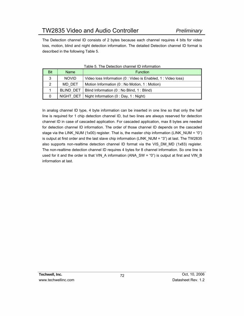
72
Techwell, Inc. www.techwellinc.com Datasheet Rev. 1.2
PreliminaryTW2835 Video and Audio Controller
Oct, 10, 2006
The Detection channel ID consists of 2 bytes because each channel requires 4 bits for video loss, motion, blind and night detection information. The detailed Detection channel ID format is described in the following Table 5.
Table 5. The Detection channel ID information Bit Name Function
3 NOVID Video loss Information (0 : Video is Enabled, 1 : Video loss) 2 MD_DET Motion Information (0 : No Motion, 1 : Motion) 1 BLIND_DET Blind Information (0 : No Blind, 1 : Blind) 0 NIGHT_DET Night Information (0 : Day, 1 : Night)
In analog channel ID type, 4 byte information can be inserted in one line so that only the half line is required for 1 chip detection channel ID, but two lines are always reserved for detection channel ID in case of cascaded application. For cascaded application, max 8 bytes are needed for detection channel ID information. The order of those channel ID depends on the cascaded stage via the LINK_NUM (1x00) register. That is, the master chip information (LINK_NUM = “0”) is output at first order and the last slave chip information (LINK_NUM = “3”) at last. The TW2835 also supports non-realtime detection channel ID format via the VIS_DM_MD (1x83) register. The non-realtime detection channel ID requires 4 bytes for 8 channel information. So one line is used for it and the order is that VIN_A information (ANA_SW = “0”) is output at first and VIN_B information at last.

73
Techwell, Inc. www.techwellinc.com Datasheet Rev. 1.2
PreliminaryTW2835 Video and Audio Controller
Oct, 10, 2006
Analog Type Channel ID in VBI The TW2835 supports the analog type channel ID during VBI period. The analog channel ID can include an Auto channel ID, Detection channel ID and User channel ID. Each channel ID can be enabled via the VIS_AUTO_EN, AUTO_RPT_EN, VIS_DET_EN, VIS_USER_EN (1x80) registers. The Auto channel ID requires one line basically, but can need one more line for repetition. Both Detection channel ID and User channel ID require two lines so that total six lines are used for analog type channel ID.
The vertical starting position of analog channel ID is controlled by the VIS_LINE_OS (1x83) register with 1 line unit and the horizontal starting position is defined via VIS_PIXEL_HOS(1x81) register with 2 pixel unit. The pixel width of each bit is controlled by the VIS_PIXEL_WIDTH (1x82) register and the magnitude of each bit is defined by the VIS_HIGH_VAL/VIS_LOW_VAL (1x84/1x85) register.
The analog channel ID consists of run-in clock, channel ID data, type and parity bit. The run-in clock insertion is enabled via the VIS_RIC_EN (1x80) register. The channel ID data can include 4 byte information and the channel ID type contains 3 bits that “0” is meant for Auto channel ID, “1” for repeated channel ID, “2” for Detection channel ID of master and first slave stage chip, “3” for Detection channel ID of second and third slave chip, “4” for User channel ID of VIS_MAN0~3, and “5” for User channel ID of VIS_MAN4~8. The parity is 1 bit width and used for even parity. The analog channel ID is located right after digital channel ID line. The following Fig 45 shows the illustration of analog channel ID.
Run-In ClockVIS_PIXEL_HOS
VBI_HW
Parity
* Channel ID Type of each line can be detected with Channel ID Type.Auto channel ID = 001 / 010 (Repeated channel ID)Detection Channel ID = 011 / 100User Channel ID = 101 / 110
Analog Channel ID Format
VIS_HIGH_VAL
Video Output
H
V
FVIS_LINE_OS + VIS_FLD_OS
A0 = 11000000 A1 = 11000001 A2 = 11000010 A2 = 11000010
Channel ID Type (*)
Digital Channel ID
User Channel ID
Detection Channel ID
Auto Channel ID
VIS_LOW_VAL
Fig 45 The illustration of analog channel ID

74
Techwell, Inc. www.techwellinc.com Datasheet Rev. 1.2
PreliminaryTW2835 Video and Audio Controller
Oct, 10, 2006
Digital Type Channel ID in VBI The TW2835 also provides the digital type channel ID during VBI period. It’s useful for DSP application because the channel ID can be inserted in just 1 line with special format. The digital channel ID is located before analog channel ID line. The digital channel ID can be enabled via the VIS_CODE_EN (1x80) register.
The digital channel ID is inserted in Y data in ITU-R BT.656 stream and composed of ID # and channel information. The ID # indicates the index of digital type channel ID including the Start code, Auto/Detection/User channel ID and End code. The ID # has 0 ~ 63 index and each channel information of 1 byte is divided into 2 bytes of 4 LSB that takes “50h” offset against ID # for discrimination. The Start code is located in ID# 0 ~ 1 and the Auto channel ID is situated in ID# 2 ~ 9. The Detection channel ID is located in ID # 10 ~ 25 and the User channel ID is situated in ID # 26 ~ 41. The End code occupies the others. The digital channel ID is repeated more than 5 times during horizontal active period. The following Fig 46 shows the illustration of the digital channel ID.
Repeated Again
Cb Y Cr Y
Horizontal Active Period (1440 Pixel)Digital Channel ID
SAV EAVP0
00h 00h 00h 5Fh 00h 01h 00h 50h 00h 02h 00h 5Ch 00h 03h 00h 50h
P1
FFh 00h 00h XYh
P1440
1st Start Code 2nd Start Code 1st Auto Channel ID 2nd Auto Channel ID
00h 3Eh 00h 50h
63th End Code
00h 3Fh 00h 50h
64th End Code
Full Ch ID Set = 256 Pixels
Digital Channel ID Format
~ 0101, U7_LSB~
~
0101, D7_LSB~ 0101, A3_LSB
63--25 ~
User Channel ID (8 Bytes)
0101, U0_MSB
26 41
Detection Channel ID (8 Bytes)
0101, D0_MSB
109~
Auto Channel ID (4 Bytes)
0101, A0_MSB
2
0101, 000050h5FhData
End CodeStart Codedescription
4210Id #
00h 00h
00h ID # 00h Data
SAV
P2 P3
Video Output
H
V
FVBI_LINE_OS + VBI_FLD_OS Digital Channel ID
Fig 46 The illustration of the digital channel ID in VBI period

75
Techwell, Inc. www.techwellinc.com Datasheet Rev. 1.2
PreliminaryTW2835 Video and Audio Controller
Oct, 10, 2006
Digital Type Channel ID in Channel Boundary The TW2835 also supports the extra type of digital channel ID in horizontal boundary of each channel. This information can be used for very easy memory management of each channel in DSP solution because this digital channel ID information includes not only the channel information but also line number of picture. The Auto channel ID format is described in the following Table 6.
Table 6 The digital channel ID information in active area Bit Name Function
[15:7] LINENUM Active Line number 6 FIELD Field Polarity Information 5 REG_EN Region Enable Information 4 ANAPATH Analog switch information
[3:2] CASCADE Cascade Stage Information [1:0] VIN_PATH Video Input Path Number (depending on DEC_PATH_Y)
This digital channel ID is enabled in the horizontal active area by setting “1” to the CH_START (1x55) register. The following Fig 47 shows the digital channel ID in channel boundary.
Cb Y Cr Y
Digital Data for Channel ID
SAV EAVP0
21h 01h 23h 01h
P1
FFh 00h 00h XYh
CH 1 Start Code
00h Linenum[7:0]
00h Data Linenum[8], ENC_FIELD, VALID, ANA_PATH, CASCADE(2 Bit), VIN_PATH(2Bit)
SAV
CH 1
Channel 1 Data
Cb Y Cr Y
22h 01h 23h 01h
CH 2 Start Code
CH 2
Cb Y Cr Y
00h 01h 23h 01h
No video Start Code
Channel 2 Data Blank Data
Horizontal Active Period
Line
#
0
23h
P2 P3 P0 P1 P2 P3 P0 P1 P2 P3
No
chan
nel A
rea
0 320 640 720
Pixel #Video Output when SIZE_MODE = 2
Fig 47 The digital channel ID format in channel boundary

76
Techwell, Inc. www.techwellinc.com Datasheet Rev. 1.2
PreliminaryTW2835 Video and Audio Controller
Oct, 10, 2006
Chip-to-Chip Cascade Operation The TW2835 supports chip-to-chip cascade connection up to 4 chips for 16-channel application and also provides the independent operation for display and record path. That is, the display path can be operated with cascade connection even though the record path is working in normal operation. Likewise, the cascade connection of record path is limited within 4 chips while the infinite cascade connection of display path can be supported for more than 16-channel application.
In cascade operation, the TW2835 transfers all information of slaver chips to master chip including video data, zoom factors, switching information and 2D box except overlay information such as single box, mouse pointer and bitmap information. Therefore, the master chip should be controlled for overlay and the lowest slaver chip should be controlled for the others such as video data, zoom control and switching queue.
Channel Priority Control When 2 channels are overlapped in chip-to-chip cascade operation for display path, there is a priority with the following order such as popup attributed channel of master device, popup attributed channel of slaver device, non-popup attributed channel of master device and non-popup attributed channel of slaver device. Using this popup attribute, the TW2835 can implement the channel overlay such as PIP, POP, and full D1 format channel switching in chip-to-chip cascade connection.
For QUAD multiplexing record output in chip-to-chip cascade application, the popup priority of the channel is controlled via the QUAD_MUX queue. The QUAD_MUX operation is enabled via the POS_CTL_EN (1x70) register and the operation mode should be set into strobe operation (FUNC_MODE = “1”). If the POS_CTL_EN is “0”, the channel position is defined via the PIC_POS (1x6D) register and the priority from top to bottom layer is controlled by the popup attribute like the display path. If the POS_CTL_EN is “1”, the channel position and priority is controlled by the pre-defined queue or interrupt.
The TW2835 supports the interrupt triggering via the POS_INTR (1x70), POS_CH (1x73, 1x74) register and also provides the internal or external triggering mode for the QUAD_MUX operation. The triggering mode is selected via the POS_TRIG_MODE (1x70) register such as “0” for external trigger mode and “1” for internal trigger mode.
The QUAD_MUX queue size can be defined by the POS_QUE_SIZE (1x71) register. To change the channel popup sequence in internal queue, the POS_QUE_WR (1x75) register should be set to “1” after defining the queue address with the POS_QUE_ADDR (1x75) register and the channel number with the POS_CH (1x73, 1x74) register. The POS_QUE_WR register will be cleared automatically after updating queue. The QUAD_MUX queue is shared with the normal switching queue so that the maximum queue size for QUAD_MUX is 32 (=128/4) depth.
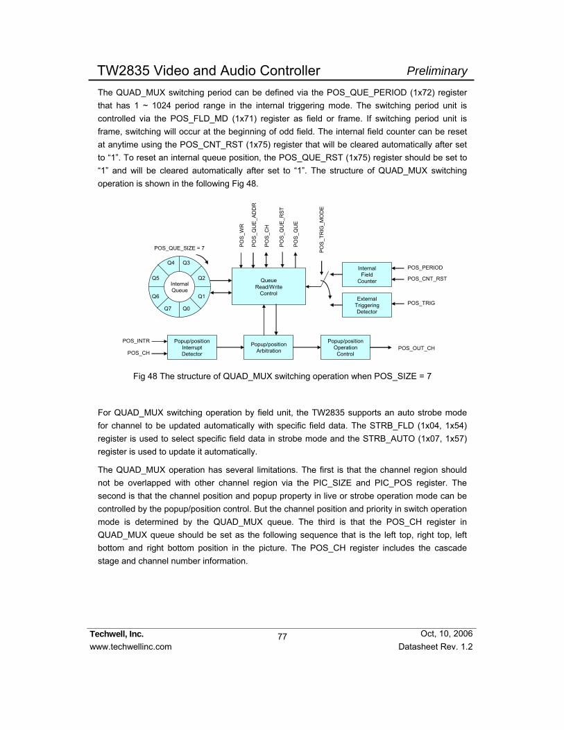
77
Techwell, Inc. www.techwellinc.com Datasheet Rev. 1.2
PreliminaryTW2835 Video and Audio Controller
Oct, 10, 2006
The QUAD_MUX switching period can be defined via the POS_QUE_PERIOD (1x72) register that has 1 ~ 1024 period range in the internal triggering mode. The switching period unit is controlled via the POS_FLD_MD (1x71) register as field or frame. If switching period unit is frame, switching will occur at the beginning of odd field. The internal field counter can be reset at anytime using the POS_CNT_RST (1x75) register that will be cleared automatically after set to “1”. To reset an internal queue position, the POS_QUE_RST (1x75) register should be set to “1” and will be cleared automatically after set to “1”. The structure of QUAD_MUX switching operation is shown in the following Fig 48.
InternalQueue
Q3
Q2
Q1
Q0Q7
Q6
Q5
Q4
QueueRead/Write
Control
POS_QUE_SIZE = 7
POS_PERIOD
Popup/positionArbitration
Popup/positionInterruptDetector
InternalField
Counter POS_CNT_RST
ExternalTriggeringDetector
POS_TRIG
POS
_TR
IG_M
OD
E
Popup/positionOperation
Control
POS_INTR
POS_CHPOS_OUT_CH
POS
_QU
E_AD
DR
PO
S_C
H
PO
S_Q
UE_
RST
POS_
QU
E
POS_
WR
Fig 48 The structure of QUAD_MUX switching operation when POS_SIZE = 7
For QUAD_MUX switching operation by field unit, the TW2835 supports an auto strobe mode for channel to be updated automatically with specific field data. The STRB_FLD (1x04, 1x54) register is used to select specific field data in strobe mode and the STRB_AUTO (1x07, 1x57) register is used to update it automatically.
The QUAD_MUX operation has several limitations. The first is that the channel region should not be overlapped with other channel region via the PIC_SIZE and PIC_POS register. The second is that the channel position and popup property in live or strobe operation mode can be controlled by the popup/position control. But the channel position and priority in switch operation mode is determined by the QUAD_MUX queue. The third is that the POS_CH register in QUAD_MUX queue should be set as the following sequence that is the left top, right top, left bottom and right bottom position in the picture. The POS_CH register includes the cascade stage and channel number information.

78
Techwell, Inc. www.techwellinc.com Datasheet Rev. 1.2
PreliminaryTW2835 Video and Audio Controller
Oct, 10, 2006
120 CIF/Sec Record Mode For chip-to-chip cascade connection, the DLINKI, VLINKI and HLINKI pin in master chip should be connected to VDOUTX, VSENC and HSENC pin in slaver chips. So the VDOUTX, VSENC and HSENC output pin is only available in master device when cascaded.
The TW2835 has several registers for cascade operation such as the LINK_EN, LINK_NUM, LINK_LAST (1x00) and SYNC_DEL (1x7E) register. For lowest slaver chip, both LINK_LAST_X and LINK_LAST_Y should be set to “1”. To receive the cascade data from slaver chip, either LINK_EN_X or LINK_EN_Y should be set to “1”. To transfer the cascade data properly among the chips, the LINK_NUM and SYNC_DEL should be set properly in accordance with its order. The information of switching channel can be taken from master chip via the channel ID in video stream output or by reading the MUX_OUT_CH (1x08, 1x6E) register. The information of switching channel can also be taken from the lowest slaver chip via the MPP1/2 pins. The following Fig 49 illustrates the cascade connection for 120 CIF/Sec record mode.
1514
1312
0~3Input
Master(LINK_NUM =0)(SYNC_DEL = 4)
(LINK_LAST_X=0,LINK_EN_X=1)
(LINK_LAST_Y=0,LINK_EN_Y=1)
Slave1(LINK_NUM=1)
(SYNC_DEL = 2)(LINK_LAST_X=0,
LINK_EN_X=1)(LINK_LAST_Y=0,
LINK_EN_Y=1)
Slave2(LINK_NUM=2)
(SYNC_DEL = 0)(LINK_LAST_X=0,
LINK_EN_X=1)(LINK_LAST_Y=0,
LINK_EN_Y=1)
Slave3(LINK_NUM=3)(SYNC_DEL=0)
(LINK_LAST_X=1,LINK_EN_X=1)
(LINK_LAST_Y=1,LINK_EN_Y=1)
Display (16ch Split)
4~7Input
8~11Input
12~15Input
VIN1VIN2VIN3
VIN0VDOUTX
VDOUTY
PBIN
VSENC
VDOUTY
VDOUTY
VSENC
VDOUTY
12
12 8 5 3
12 8
12 8 5
13
Record (16ch MUX)
8 8 13
5 13
time
switchswitch
switch
switch
switch
time
time
time
12 12 12 13
1551181232146131007914
X
X
X
155118121461310794
151214
13
151181214
13109
2
1
2
1
3
4
5
4 5
PBIN
PBIN
PBIN
VDOUTX
1110
98
76
54
1514
1312
1110
98
1110
98
1514
1312
1514
1312
1514
1312
1514
1312
1110
98
76
54
Record (Quad MUX)
32
10
76
54
1110
98
1514
1312
Pop_up
Pop_up
Pop_up
Pop_up
VDOUTX
VSENCVDOUTX
3
HLINKIVLINKI DLINKI
PB Input
VIN1VIN2VIN3
VIN0
VIN1VIN2VIN3
VIN0
VIN1VIN2VIN3
VIN0
5
HLINKIVLINKI DLINKI
HLINKIVLINKI DLINKI
HLINKIVLINKI DLINKI
Fig 49 The cascade connection for 120 CIF/sec record mode
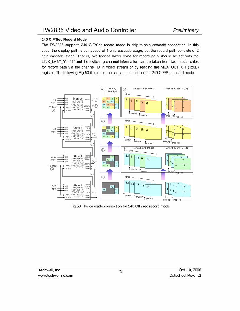
79
Techwell, Inc. www.techwellinc.com Datasheet Rev. 1.2
PreliminaryTW2835 Video and Audio Controller
Oct, 10, 2006
240 CIF/Sec Record Mode The TW2835 supports 240 CIF/Sec record mode in chip-to-chip cascade connection. In this case, the display path is composed of 4 chip cascade stage, but the record path consists of 2 chip cascade stage. That is, two lowest slaver chips for record path should be set with the LINK_LAST_Y = “1” and the switching channel information can be taken from two master chips for record path via the channel ID in video stream or by reading the MUX_OUT_CH (1x6E) register. The following Fig 50 illustrates the cascade connection for 240 CIF/Sec record mode.
76
54
0~3Input
Master(LINK_NUM =0)(SYNC_DEL = 4)
(LINK_LAST_X=0,LINK_EN_X=1)
(LINK_LAST_Y=0,LINK_EN_Y=1)
Slave1(LINK_NUM=1)
(SYNC_DEL = 2)(LINK_LAST_X=0,
LINK_EN_X=1)(LINK_LAST_Y=1,
LINK_EN_Y=1)
Slave2(LINK_NUM=2)
(SYNC_DEL = 0)(LINK_LAST_X=0,
LINK_EN_X=1)(LINK_LAST_Y=0,
LINK_EN_Y=1)
Slave3(LINK_NUM=3)
(SYNC_DEL = 0)(LINK_LAST_X=1,
LINK_EN_X=1)(LINK_LAST_Y=1,
LINK_EN_Y=1)
Display (16ch Split)
4~7Input
8~11Input
12~15Input
VIN1VIN2VIN3
VIN0VDOUTX
VDOUTY
PBIN
VSENC
VDOUTY
VDOUTY
VSENC
VDOUTY
12
4 2 5 3
12 8
4 4 5
6
Record (8ch MUX)
13 9 14
5 6
time
switchswitch
switch
switch
switch
time
time
time
12 13 13 14
1551181232146131007914
X
X
switch
155118121461310794
151214
13
151181214
13109
2
1
2
1
3
4
6
4 6
PBIN
PBIN
PBIN
HSENC
VDOUTX
76
54
76
54
1514
1312
1110
98
1514
1312
1514
1312
1514
1312
76
54
32
10
76
54
Record (Quad MUX)
32
10
76
54
1514
1312
Pop_up
Pop_up
Pop_up
VDOUTX
VSENC
HSENCVDOUTX
3
HLINKIVLINKI DLINKI
HSENC
PB Input
VIN1VIN2VIN3
VIN0
VIN1VIN2VIN3
VIN0
VIN1VIN2VIN3
VIN0
1514
1312
1110
98
switch
switch
switch
switch
5
5 Record (8ch MUX) Record (Quad MUX)
PB Input
6
5
Pop_up
Pop_up
Pop_up
Pop_up
Pop_up
HLINKIVLINKI DLINKI
HLINKIVLINKI DLINKI
HLINKIVLINKI DLINKI
Fig 50 The cascade connection for 240 CIF/sec record mode

80
Techwell, Inc. www.techwellinc.com Datasheet Rev. 1.2
PreliminaryTW2835 Video and Audio Controller
Oct, 10, 2006
480 CIF/Sec Record Mode The TW2835 also supports 480 CIF/Sec record mode in chip-to-chip cascade connection. In this case, the display path is composed of 4 chip cascade stage, but the record path has no cascade connection. Even though the record path has no cascade connection, the LINK_NUM should be set properly in accordance with its cascade order for correct channel number in channel ID and the LINK_EN_Y should be set to “0” or the LINK_LAST_Y should be set to “1”. The TW2835 transfers the slaver chip information to master chip such as zoom control and 2D box only for display path and the switching channel information for record path can be taken from each chip via the channel ID in video stream or by reading the MUX_OUT_CH (1x6E) register. The following Fig 51 illustrates the cascade connection for 480 CIF/Sec record mode.
Display (16ch Split)
15
0 1 2 3
8 9
5 7 4
10 11
6
time
time
time
time
12 13 14
1551181232146131007914
155118121461310794
151214
13
151181214
13109
32
10
76
54
1110
98
1415
1312
Record (4ch MUX or QUAD)
Record (4ch MUX or QUAD)
Record (4ch MUX or QUAD)
Record (4ch MUX or QUAD)
5
6
7
8
1
2
3
4
0~3 InputMaster
(LINK_NUM=0)(SYNC_DEL = 4)
(LINK_LAST_X=0,LINK_EN_X=1)
(LINK_LAST_Y=0,LINK_EN_Y=0)
Slave1(LINK_NUM=1)
(SYNC_DEL = 2)(LINK_LAST_X=0,
LINK_EN_X=1)(LINK_LAST_Y=0,
LINK_EN_Y=0)
Slave2(LINK_NUM=2)
(SYNC_DEL = 0)(LINK_LAST_X=0,
LINK_EN_X=1)(LINK_LAST_Y=0,
LINK_EN_Y=0)
Slave3(LINK_NUM=3)
(SYNC_DEL = 0)(LINK_LAST_X=1,
LINK_EN_X=1)(LINK_LAST_Y=1,
LINK_EN_Y=0)PB Input
4~7 Input
8~11 Input
12~15 Input
VIN0VIN1VIN2VIN3
VDOUTX
VDOUTY
HLINKI
VIN0VIN1VIN2VIN3
PBIN
VSENC
VDOUTY
3
4
8PBINVLINKI
VDOUTX
7
DLINKI
PB Input
VSENC
VDOUTY
VDOUTX
6
VSENC
VDOUTY
VDOUTX
5
2
PBIN
1
PBINPB Input
PB Input
8
7
6
5
VIN0VIN1VIN2VIN3
VIN0VIN1VIN2VIN3
HLINKIVLINKIDLINKI
HLINKIVLINKIDLINKI
HLINKIVLINKI
DLINKI
Fig 51 The cascade connection for 480 CIF/Sec record mode

81
Techwell, Inc. www.techwellinc.com Datasheet Rev. 1.2
PreliminaryTW2835 Video and Audio Controller
Oct, 10, 2006
Infinite Cascade Mode for Display Path In normal cascade connection, the master chip has LINK_NUM = “0” and the lowest slaver chip has LINK_NUM = “3”. The master chip can output both display and record path, but the slaver device can output only record path. To implement more than 16 channel application, the TW2835 also provides the infinity cascade connection for display path. That is, the video data and popup information can be transferred to next cascade chip even though the master chip is set with LINK_NUM = “0” and the slaver chip with LINK_NUM = “3” for display path. This mode can be enabled via the T_CASCADE_EN (1x7F) register.
The following Fig 52 illustrates the multiple cascade connection for display path. In this example, the display path in the last master chip can output 32 channel video and the record path can implement “480 CIF/sec” with lower 4 chips and “120 CIF/sec” with upper 4 chips.
M id d leM a s te r
(L IN K _ N U M = 0 )(T _ C A S C A D E _ E N = 1 )
(S Y N C _ D E L = 4 )(L IN K _ L A S T _ X = 0 ,
L IN K _ E N _ X = 1 )(L IN K _ L A S T _ Y = 0 ,
L IN K _ E N _ Y = 0 )
L o w e stS la ve 3
(L IN K _ N U M = 3 )(S Y N C _ D E L = 0 )
(L IN K _ L A S T _ X = 1 ,L IN K _ E N _ X = 1 )
(L IN K _ L A S T _ Y = 1 ,L IN K _ E N _ Y = 0 )
D isp la y (m u lt i-ch S p lit)
V id e oIn p u t
V id e oIn p u t
P B IN
V D O U T Y
V S E N C
V D O U T Y
3 4 B D
0 1
0
C a p tu re (1 6 c h M U X )
2 3 1
FEDCBA9
1 2 3 4 765
5
D FECBA98
8
1 3 6 7420
0
P B IN32
10
76
54
32
10
BA
98
C a p tu re (Q U A D M U X )
FE
DC
V D O U T X
V S E N CV D O U T XV IN 1
V IN 2V IN 3
V IN 0
V IN 1V IN 2V IN 3
V IN 0
1
C a p tu re (4 c h M U X ) C a p tu re (Q u a d )
4
6
FEDCBA9
5
D FEC
8
1 3 6 7420
FEDCBA9
5
8
1 3 6 7420H L IN K I
V L IN K I D L IN K I
H L IN K IV L IN K I D L IN K I
M id d leS la v e 1
(L IN K _ N U M = 1 )(S Y N C _ D E L = 2 )
(L IN K _ L A S T _ X = 0 ,L IN K _ E N _ X = 1 )
(L IN K _ L A S T _ Y = 0 ,L IN K _ E N _ Y = 0 )
V id e oIn p u t
P B IN
V S E N C
V D O U T Y
V D O U T XV IN 1V IN 2V IN 3
V IN 0
3H L IN K I
V L IN K I D L IN K I
H S E N C
M id d leS la v e 2
(L IN K _ N U M = 2 )(S Y N C _ D E L = 0 )
(L IN K _ L A S T _ X = 0 ,L IN K _ E N _ X = 1 )
(L IN K _ L A S T _ Y = 0 ,L IN K _ E N _ Y = 0 )
V id e oIn p u t
P B IN
V S E N C
V D O U T Y
V D O U T XV IN 1V IN 2V IN 3
V IN 0
2H L IN K I
V L IN K I D L IN K I
7 5 4 7 6 76
54
C a p tu re (4 c h M U X ) C a p tu re (Q u a d )
FEDCBA9
5
8
6 74
8 9 B A 8 8A
B9
C a p tu re (4 c h M U X ) C a p tu re (Q u a d )
FEDCBA98
FEDC
C D E F C FE
DC
C a p tu re (4 c h M U X ) C a p tu re (Q u a d )
FEDCBA9
5
D FECBA98
8
1 3 6 7420
FEDCBA9
4 765
5
D FECBA98
8
1 3 6 7420
M a s te rD e v ic e
(L IN K _ N U M = 0 )(S Y N C _ D E L = 6 )
(L IN K _ L A S T _ X = 0 ,L IN K _ E N _ X = 1 )
(L IN K _ L A S T _ Y = 0 ,L IN K _ E N _ Y = 1 )
M id d leS la ve 3
(L IN K _ N U M = 3 )(T _ C A S C A D E _ E N = 1 )
(S Y N C _ D E L = 0 )(L IN K _ L A S T _ X = 0 ,
L IN K _ E N _ X = 1 )(L IN K _ L A S T _ Y = 1 ,
L IN K _ E N _ Y = 1 )
V ide oIn p u t
V ide oIn p u t
P B IN
V D O U T Y
V S E N C
V D O U T Y
P B IN
V D O U T X
V D O U T XV IN 1V IN 2V IN 3
V IN 0
V IN 1V IN 2V IN 3
V IN 0
H L IN K IV L IN K I D L IN K I
H L IN K IV L IN K I D L IN K I
M id d leS la v e 1
(L IN K _ N U M = 1 )(S Y N C _ D E L = 4 )
(L IN K _ L A S T _ X = 0 ,L IN K _ E N _ X = 1 )
(L IN K _ L A S T _ Y = 0 ,L IN K _ E N _ Y = 1 )
V ide oIn p u t
P B IN
V S E N C
V D O U T Y
V D O U T XV IN 1V IN 2V IN 3
V IN 0
H L IN K IV L IN K I D L IN K I
M id d leS la v e 2
(L IN K _ N U M = 2 )(S Y N C _ D E L = 2 )
(L IN K _ L A S T _ X = 0 ,L IN K _ E N _ X = 1 )
(L IN K _ L A S T _ Y = 0 ,L IN K _ E N _ Y = 1 )
V ide oIn p u t
P B IN
V S E N C
V D O U T Y
V D O U T XV IN 1V IN 2V IN 3
V IN 0
H L IN K IV L IN K I D L IN K I
6
5
5
1
4
3
2
6
1
4
3
2
Fig 52 Infinite cascade mode for display path
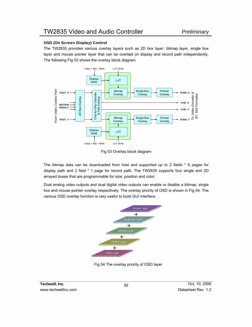
82
Techwell, Inc. www.techwellinc.com Datasheet Rev. 1.2
PreliminaryTW2835 Video and Audio Controller
Oct, 10, 2006
OSD (On Screen Display) Control The TW2835 provides various overlay layers such as 2D box layer, bitmap layer, single box layer and mouse pointer layer that can be overlaid on display and record path independently. The following Fig 53 shows the overlay block diagram.
2D B
ox O
verla
y
Single BoxOverlay
BitmapOverlay
PointerOverlay
LUTDisplayRAM
BitmapOverlay
PointerOverlay
LUTDisplayRAM
LUT Write
VOSD_Y
Index + Mix + Blink
LUT WriteIndex + Mix + Blink
VOSD_X
VVID_X
VVID_Y
VOUT_X
MOTIONRESULT
VOUT_Y
From
Vid
eo C
ontro
l Par
t
To V
ideo
Enc
oder
&BT
. 656
For
mat
ter
Chi
p-to
-Chi
p C
asca
de&
Pat
h O
verla
y
Single BoxOverlay
Fig 53 Overlay block diagram
The bitmap data can be downloaded from host and supported up to 2 fields * 6 pages for display path and 2 field * 1 page for record path. The TW2835 supports four single and 2D arrayed boxes that are programmable for size, position and color.
Dual analog video outputs and dual digital video outputs can enable or disable a bitmap, single box and mouse pointer overlay respectively. The overlay priority of OSD is shown in Fig 54. The various OSD overlay function is very useful to build GUI interface.
Bitmap Layer
Single box Layer
Pointer Layer
Video Layer
2D Box Layer
Fig 54 The overlay priority of OSD layer

83
Techwell, Inc. www.techwellinc.com Datasheet Rev. 1.2
PreliminaryTW2835 Video and Audio Controller
Oct, 10, 2006
2 Dimensional Arrayed Box The TW2835 supports four 2D arrayed boxes that have programmable cell size up to 16x16. The 2D arrayed box can be used to make table menu or display motion detection information via the 2DBOX_MODE (2x60, 2x68, 2x70, 2x78) register. The 2D arrayed box is displayed on each path by the 2DBOX_EN (2x60, 2x68, 2x70, and 2x78) register.
For each 2D arrayed box, the number of row and column cells is defined via the 2DBOX_HNUM and 2DBOX_VNUM (2x66, 2x6E, 2x76, and 2x7E) registers. The horizontal and vertical location of left top is controlled by the 2DBOX_HL (2x62, 2x6A, 2x72, and 2x7A) register and the 2DBOX_VT (2x64, 2x6C, 2x74, and 2x7C) registers. The horizontal and vertical size of each cell is defined by the 2DBOX_VW (2x65, 2x6D, 2x75, and 2x7D) registers and the 2DBOX_HW (2x63, 2x6B, 2x73, and 2x7B) registers. So the whole size of 2D arrayed box is same as the sum of cells in row and column.
The boundary of 2D arrayed box is enabled by the 2DBOX_BNDEN (2x61, 2x69, 2x71, and 2x79) register and its color is controlled via the 2DBOX_BNDCOL (2x5F) register which selects one of 4 colors such as 0% black, 25% gray, 50% gray and 75% white.
Especially the TW2835 provides the function to indicate cursor cell inside 2D arrayed box. The cursor cell is enabled by the 2DBOX_CUREN (2x60, 2x68, 2x70, and 2x78) register and the displayed location is defined by the 2DBOX_CURHP and 2DBOX_CURVP (2x67, 2x6F, 2x77, and 2x7F) registers. Its color is a reverse color of cell boundary. It is useful function to control motion mask region.
The plane of 2D arrayed box is separated into mask plane and detection plane. The mask plane represents the cell defined by MD_MASK (2x86 ~ 2x9D, 2xA6 ~ 2xBD, 2xC6 ~ 2xDD, 2xE6 ~ 2xFD) register. The detection plane represents the motion detected cell excluding the mask cells among whole cells. The mask plane of 2D arrayed box is enabled by the 2DBOX_MSKEN (2x60, 2x68, 2x70, 2x78) register and the detection plane is enabled by the 2DBOX_DETEN (2x60, 2x68, 2x70, 2x78) register. The color of mask plane is controlled by the MASK_COL (2x5B ~ 2x5E) register and the color of detection plane is defined by the DET_COL (2x5B ~ 2x5E) register which selects one out of 12 fixed colors or 4 user defined colors using the CLUT (2x13 ~ 2x1E) register. The mask plane of 2D arrayed box shows the mask information according to the MD_MASK registers automatically and the additional narrow boundary of each cell is provided to display motion detection via the 2DBOX_DETEN register and its color is a reverse cell boundary color. The plane can be mixed with video data by the 2DBOX_MIX (2x60, 2x68, 2x70, 2x78) register and the alpha blending level is controlled as 25%, 50%, and 75% via the ALPHA_2DBOX (2x1F) register. Even in the horizontal / vertical mirroring mode, the video data and motion detection result can be matched via the 2DBOX_HINV and 2DBOX_VINV (2x81, 2xA1, 2xC1, 2xE1) registers.
The TW2835 has 4 2D arrayed boxes so that 4 video channels can have its own 2D arrayed box for motion display mode. To overlay mask information and motion result on video data properly, the scaling ratio of video should be matched with 2D arrayed box size.

84
Techwell, Inc. www.techwellinc.com Datasheet Rev. 1.2
PreliminaryTW2835 Video and Audio Controller
Oct, 10, 2006
The following Fig 55 shows the 2D arrayed box of table mode and motion display mode.
Detection Plane (MD_MASK = 0) : Color by DET_COL
Boundary
2DBOX_HW
2DBOX_HL2D
BOX_
VT
2DBO
X_VW
2DB
OX_
VNU
M =
42DBOX_HNUM = 7
Cursor Cell 2DBOX_CUR_HP = 5 2DBOX_CUR_VP = 1
Mask Plane (MD_MASK = 1) : Color by MASK_COL Mask Plane
Boundary
Motion detected
Cell
No Motion Cell
2DBOX_HNUM = 15
2DBO
X_V
NU
M =
11
Detection Plane
Table mode Motion display mode in 2DBOX_DETEN = 0
Fig 55 The 2D arrayed box in table mode and motion display mode
In case those several 2D arrayed boxes have same region, there will be a conflict of what to display for that region. Generally the TW2835 defines that 2D arrayed box 0 has priority over other 2D arrayed box. So if a conflict happens between more than 2 2D arrayed boxes, 2D arrayed box 0 will be displayed first as top layer and 2D arrayed box 1, box 2, and box 3 are hidden beneath that are not supported for pop-up attribute like channel attribute.
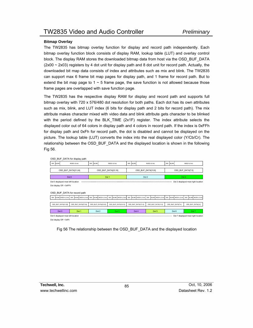
85
Techwell, Inc. www.techwellinc.com Datasheet Rev. 1.2
PreliminaryTW2835 Video and Audio Controller
Oct, 10, 2006
Bitmap Overlay The TW2835 has bitmap overlay function for display and record path independently. Each bitmap overlay function block consists of display RAM, lookup table (LUT) and overlay control block. The display RAM stores the downloaded bitmap data from host via the OSD_BUF_DATA (2x00 ~ 2x03) registers by 4 dot unit for display path and 8 dot unit for record path. Actually, the downloaded bit map data consists of index and attributes such as mix and blink. The TW2835 can support max 6 frame bit map pages for display path, and 1 frame for record path. But to extend the bit map page to 1 ~ 5 frame page, the save function is not allowed because those frame pages are overlapped with save function page.
The TW2835 has the respective display RAM for display and record path and supports full bitmap overlay with 720 x 576/480 dot resolution for both paths. Each dot has its own attributes such as mix, blink, and LUT index (6 bits for display path and 2 bits for record path). The mix attribute makes character mixed with video data and blink attribute gets character to be blinked with the period defined by the BLK_TIME (2x1F) register. The index attribute selects the displayed color out of 64 colors in display path and 4 colors in record path. If the index is 0xFFh for display path and 0xFh for record path, the dot is disabled and cannot be displayed on the picture. The lookup table (LUT) converts the index into the real displayed color (Y/Cb/Cr). The relationship between the OSD_BUF_DATA and the displayed location is shown in the following Fig 56.
OSD_BUF_DATA for display path
OSD_BUF_DATA for record path
MIX BLINK INDEX (6 bit)
MIX BLINK INDEX (2 bit) MIX BLINK INDEX (2 bit)
OSD_BUF_DATA[11:8] OSD_BUF_DATA[3:0]OSD_BUF_DATA[7:4]OSD_BUF_DATA[15:12]OSD_BUF_DATA[19:16]OSD_BUF_DATA[23:20]OSD_BUF_DATA[27:24]OSD_BUF_DATA[31:28]
OSD_BUF_DATA[7:0]OSD_BUF_DATA[15:8]OSD_BUF_DATA[23:16]OSD_BUF_DATA[31:24]
MIX BLINK INDEX (6 bit) MIX BLINK INDEX (6 bit) MIX BLINK INDEX (6 bit)
MIX BLINK INDEX (2 bit) MIX BLINK INDEX (2 bit) MIX BLINK INDEX (2 bit) MIX BLINK INDEX (2 bit) MIX BLINK INDEX (2 bit) MIX BLINK INDEX (2 bit)
Dot 5 Dot 7Dot 6Dot 4Dot 3Dot 2Dot 1Dot 0
Dot 3Dot 2Dot 1Dot 0
Dot 0 displayed most left location Dot 7 displayed most right location
Dot 0 displayed most left location Dot 3 displayed most right location
Dot display Off = 0xFFh
Dot display Off = 0xFh
Fig 56 The relationship between the OSD_BUF_DATA and the displayed location
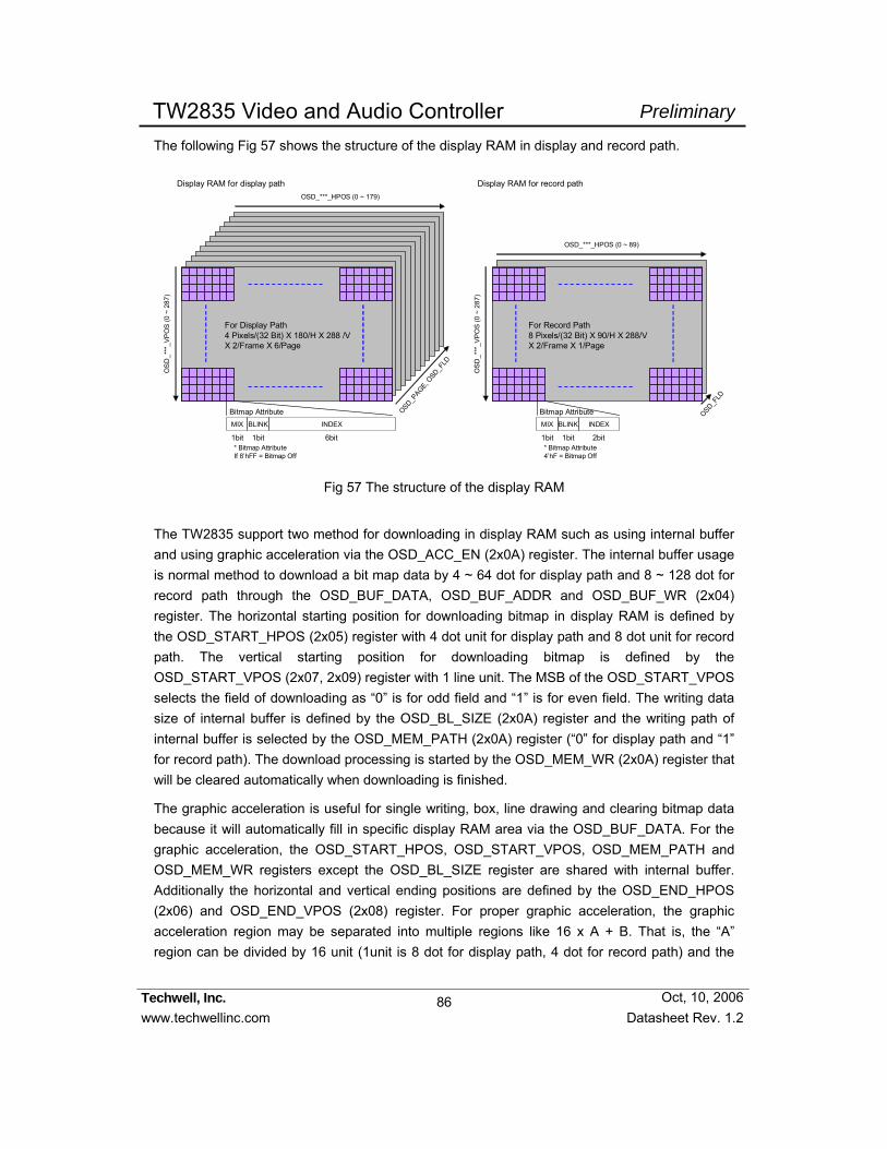
86
Techwell, Inc. www.techwellinc.com Datasheet Rev. 1.2
PreliminaryTW2835 Video and Audio Controller
Oct, 10, 2006
The following Fig 57 shows the structure of the display RAM in display and record path.
OSD_***_HPOS (0 ~ 179)
OS
D_*
**_V
PO
S (0
~ 2
87)
Bitmap AttributeMIX BLINK INDEX
1bit 1bit 6bit
For Display Path 4 Pixels/(32 Bit) X 180/H X 288 /V X 2/Frame X 6/Page
* Bitmap AttributeIf 8’hFF = Bitmap Off
Display RAM for display path
OSD_***_HPOS (0 ~ 89)
OS
D_*
**_V
PO
S (0
~ 2
87)
Bitmap AttributeMIX BLINK INDEX
1bit 1bit 2bit* Bitmap Attribute4’hF = Bitmap Off
For Record Path 8 Pixels/(32 Bit) X 90/H X 288/V X 2/Frame X 1/Page
OSD_PAGE, O
SD_FLD
Display RAM for record path
OSD_FLD
Fig 57 The structure of the display RAM
The TW2835 support two method for downloading in display RAM such as using internal buffer and using graphic acceleration via the OSD_ACC_EN (2x0A) register. The internal buffer usage is normal method to download a bit map data by 4 ~ 64 dot for display path and 8 ~ 128 dot for record path through the OSD_BUF_DATA, OSD_BUF_ADDR and OSD_BUF_WR (2x04) register. The horizontal starting position for downloading bitmap in display RAM is defined by the OSD_START_HPOS (2x05) register with 4 dot unit for display path and 8 dot unit for record path. The vertical starting position for downloading bitmap is defined by the OSD_START_VPOS (2x07, 2x09) register with 1 line unit. The MSB of the OSD_START_VPOS selects the field of downloading as “0” is for odd field and “1” is for even field. The writing data size of internal buffer is defined by the OSD_BL_SIZE (2x0A) register and the writing path of internal buffer is selected by the OSD_MEM_PATH (2x0A) register (“0” for display path and “1” for record path). The download processing is started by the OSD_MEM_WR (2x0A) register that will be cleared automatically when downloading is finished.
The graphic acceleration is useful for single writing, box, line drawing and clearing bitmap data because it will automatically fill in specific display RAM area via the OSD_BUF_DATA. For the graphic acceleration, the OSD_START_HPOS, OSD_START_VPOS, OSD_MEM_PATH and OSD_MEM_WR registers except the OSD_BL_SIZE register are shared with internal buffer. Additionally the horizontal and vertical ending positions are defined by the OSD_END_HPOS (2x06) and OSD_END_VPOS (2x08) register. For proper graphic acceleration, the graphic acceleration region may be separated into multiple regions like 16 x A + B. That is, the “A” region can be divided by 16 unit (1unit is 8 dot for display path, 4 dot for record path) and the
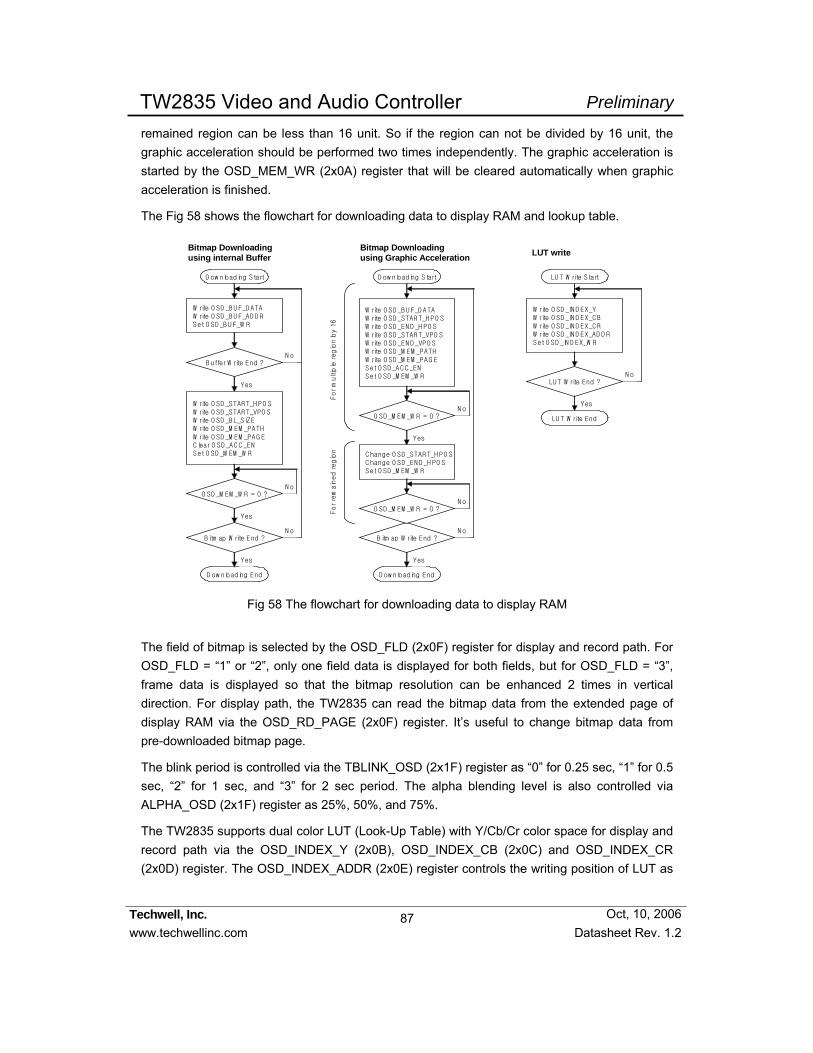
87
Techwell, Inc. www.techwellinc.com Datasheet Rev. 1.2
PreliminaryTW2835 Video and Audio Controller
Oct, 10, 2006
remained region can be less than 16 unit. So if the region can not be divided by 16 unit, the graphic acceleration should be performed two times independently. The graphic acceleration is started by the OSD_MEM_WR (2x0A) register that will be cleared automatically when graphic acceleration is finished.
The Fig 58 shows the flowchart for downloading data to display RAM and lookup table.
Bitmap Downloading using internal Buffer
D ow nloading Start
D ow nloading End
W rite O SD _B U F_D ATAW rite O SD _B U F_AD D RSet O SD _B U F_W R
B uffer W rite End ?N o
Yes
W rite O SD _STAR T_H PO SW rite O SD _STAR T_VPO SW rite O SD _B L_SIZEW rite O SD _M EM _PATHW rite O SD _M EM _PAG EC lear O SD _AC C _ENSet O SD _M EM _W R
O SD _M EM _W R = 0 ?
Yes
N o
Bitmap Downloading using Graphic Acceleration
D ow nloading Start
D ow nloading End
W rite O SD _B U F_D ATAW rite O SD _STAR T_H PO SW rite O SD _EN D _H PO SW rite O SD _STAR T_VPO SW rite O SD _EN D _VPO SW rite O SD _M EM _PATHW rite O SD _M EM _PAG ESet O SD _AC C _ENSet O SD _M EM _W R
O SD _M EM _W R = 0 ?
Yes
N o
B itm ap W rite End ?
Yes
N oB itm ap W rite End ?
Yes
N o
LUT write
LU T W rite Start
W rite O SD _IN D EX_YW rite O SD _IN D EX_C BW rite O SD _IN D EX_C RW rite O SD _IN D EX_AD D RSet O SD _IN D EX_W R
LU T W rite End ?N o
Yes
LU T W rite End
C hange O SD _STAR T_H PO SC hange O SD _EN D _H PO SSet O SD _M EM _W R
O SD _M EM _W R = 0 ?N o
For multiple region by 16
For remained region
Fig 58 The flowchart for downloading data to display RAM
The field of bitmap is selected by the OSD_FLD (2x0F) register for display and record path. For OSD_FLD = “1” or “2”, only one field data is displayed for both fields, but for OSD_FLD = “3”, frame data is displayed so that the bitmap resolution can be enhanced 2 times in vertical direction. For display path, the TW2835 can read the bitmap data from the extended page of display RAM via the OSD_RD_PAGE (2x0F) register. It’s useful to change bitmap data from pre-downloaded bitmap page.
The blink period is controlled via the TBLINK_OSD (2x1F) register as “0” for 0.25 sec, “1” for 0.5 sec, “2” for 1 sec, and “3” for 2 sec period. The alpha blending level is also controlled via ALPHA_OSD (2x1F) register as 25%, 50%, and 75%.
The TW2835 supports dual color LUT (Look-Up Table) with Y/Cb/Cr color space for display and record path via the OSD_INDEX_Y (2x0B), OSD_INDEX_CB (2x0C) and OSD_INDEX_CR (2x0D) register. The OSD_INDEX_ADDR (2x0E) register controls the writing position of LUT as

88
Techwell, Inc. www.techwellinc.com Datasheet Rev. 1.2
PreliminaryTW2835 Video and Audio Controller
Oct, 10, 2006
“0 ~ 63” is for LUT of display path and “64 ~ 67” for record path. The update processing of color LUT is started by the OSD_INDEX_WR (2x0E) register that will be cleared automatically when downloading is finished.
The TW2835 also provides bitmap overlay function between display and record path via the OSD_OVL_MD (2x38) register as “0” for no overlay, “1” for low priority overlay, “2” for high priority overlay, and “3” for only the other path overlay. The following Fig 59 shows the bitmap overlay function between display and record path.
(D isplay Path)
O SD _O VL_M D = 0 O SD _O VL_M D = 1 O SD _O VL_M D = 2 O SD _O VL_M D = 3
(Record Path)
O nly D D + R D + R O nly R
D isplay R AM
O nly R R + D R + D O nly D
O SD _O VL_M D = 0 O SD _O VL_M D = 1 O SD _O VL_M D = 2 O SD _O VL_M D = 3
Fig 59 The bitmap overlay function between display and record path
89
Techwell, Inc. www.techwellinc.com Datasheet Rev. 1.2
PreliminaryTW2835 Video and Audio Controller
Oct, 10, 2006
Single Box The TW2835 provides 4 single boxes that can be used for picture masking or box cursor. Each single box has programmable location and size parameters with the BOX_HL (2x22, 2x28, 2x2D, 2x34), BOX_HW (2x23, 2x29, 2x2E, 2x35), BOX_VT (2x24, 2x2A, 2x2F, 2x36) and BOX_VW (2x25, 2x2B, 2x30, 2x37) registers. The BOX_HL is the horizontal location of box with 2 pixel unit and the BOX_HW is the horizontal size of box with 2 pixel unit. The BOX_VT is the vertical location of box with 1 line unit and the BOX_VW is the vertical size of box with 1 line unit.
The BOX_PLNEN (2x20, 2x26, 2x2B, 2x32) register enables each plane color and its color is defined by the BOX_PLNCOL (2x21, 2x27, 2x2C, 2x33) register, which selects one out of 12 fixed colors or 4 user defined colors using the CLUT (2x13 ~ 2x1E) register. Each box plane can be mixed with video data via the BOX_PLNMIX (2x20, 2x26, 2x2B, 2x32) register and the alpha blending level is controlled via the ALPHA_BOX (2x1F) register.
The color of box boundary is enabled via the BOX_BNDEN (2x20, 2x26, 2x2B, 2x32) register and its color is defined by the BOX_BNDCOL (2x20, 2x26, 2x2B, 2x32) registers.
In case that several boxes have same region, there will be a conflict of what to display for that region. Generally the TW2835 defines that box 0 has priority over box 3. So if a conflict happens between more than 2 boxes, box 0 will be displayed first as top layer and box 1 to box 3 are hidden beneath that are not supported for pop-up attribute unlike channel display.
Mouse Pointer The TW2835 supports the mouse pointer that has attributes such as pointer enabling, pointer location, blink and sub-layer enabling. The mouse pointer can be overlaid on both display and record path independently.
The mouse pointer is located in the full screen according to the CUR_HP (2x11) register with 2 pixel step and CUR_VP (2x12) register with 1 line step. Two kinds of mouse pointer are provided through the CUR_TYPE (2x10) register. The CUR_SUB (2x10) register determines a pointer inside area to be filled with 100% white or to be transparent and the CUR_BLINK (2x10) register controls a blink function of mouse. Actually the CUR_ON (2x10) register enables or disables the mouse pointer for display and record path independently.
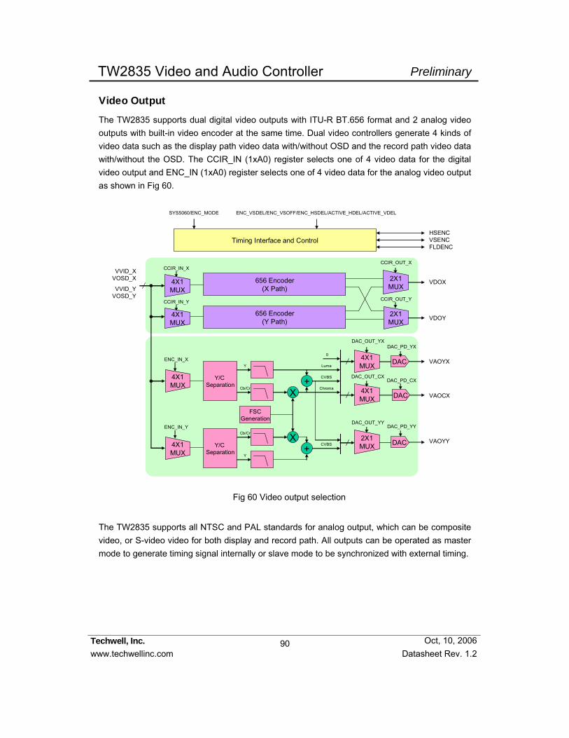
90
Techwell, Inc. www.techwellinc.com Datasheet Rev. 1.2
PreliminaryTW2835 Video and Audio Controller
Oct, 10, 2006
Video Output
The TW2835 supports dual digital video outputs with ITU-R BT.656 format and 2 analog video outputs with built-in video encoder at the same time. Dual video controllers generate 4 kinds of video data such as the display path video data with/without OSD and the record path video data with/without the OSD. The CCIR_IN (1xA0) register selects one of 4 video data for the digital video output and ENC_IN (1xA0) register selects one of 4 video data for the analog video output as shown in Fig 60.
Timing Interface and ControlHSENCVSENCFLDENC
SYS5060/ENC_MODE ENC_VSDEL/ENC_VSOFF/ENC_HSDEL/ACTIVE_HDEL/ACTIVE_VDEL
VVID_XVOSD_X
DAC_PD_YX
VVID_YVOSD_Y
VDOX
VDOY
CCIR_OUT_X
CVBS VAOYY
2X1MUX
2X1MUX
VAOYX
VAOCX
CCIR_IN_X
4X1MUX
ENC_IN_Y
4X1MUX
CCIR_IN_Y
4X1MUX
DAC_PD_CX
DAC_PD_YY
DAC
656 Encoder(X Path)
656 Encoder(Y Path)
ENC_IN_X
4X1MUX
CVBS
Luma
Chroma
Y/C Separation
Y/C Separation
+
+
FSCGeneration
X
X
DAC
DAC
DAC_PD_YX0
DAC_OUT_YX
Cb/Cr
Cb/Cr
Y
Y
DAC_OUT_CX
DAC_OUT_YY
CCIR_OUT_Y
4X1MUX
2X1MUX
4X1MUX
Fig 60 Video output selection
The TW2835 supports all NTSC and PAL standards for analog output, which can be composite video, or S-video video for both display and record path. All outputs can be operated as master mode to generate timing signal internally or slave mode to be synchronized with external timing.
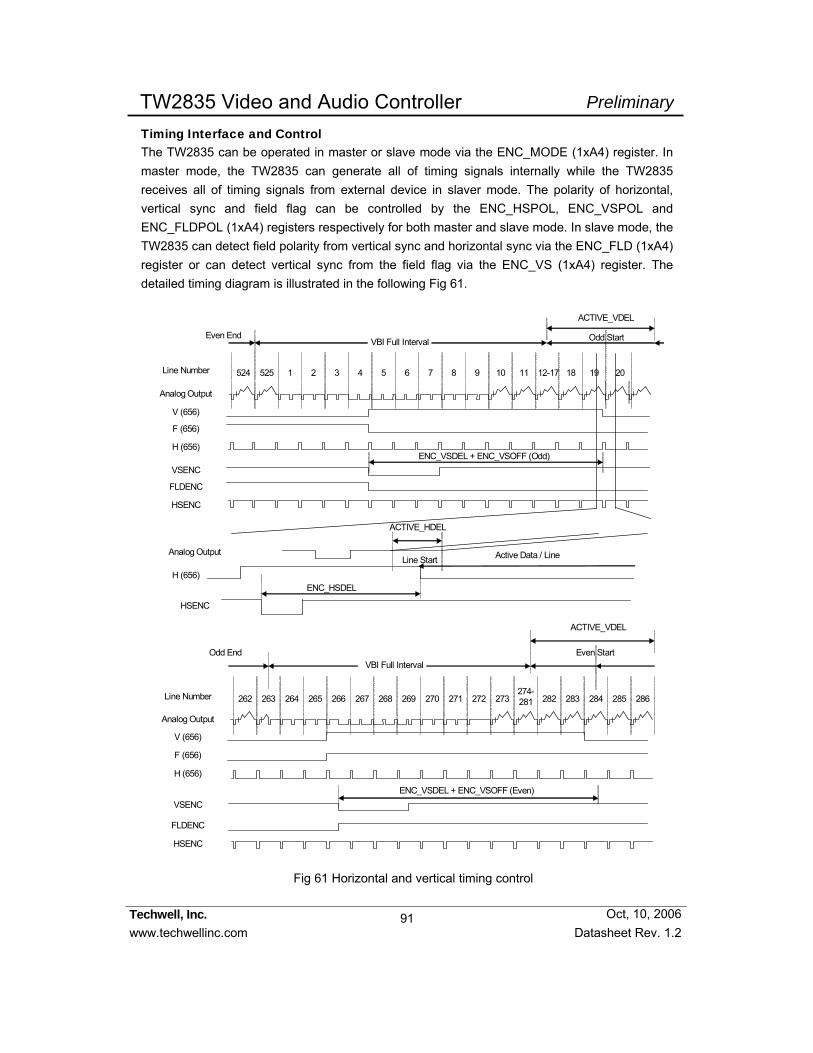
91
Techwell, Inc. www.techwellinc.com Datasheet Rev. 1.2
PreliminaryTW2835 Video and Audio Controller
Oct, 10, 2006
Timing Interface and Control The TW2835 can be operated in master or slave mode via the ENC_MODE (1xA4) register. In master mode, the TW2835 can generate all of timing signals internally while the TW2835 receives all of timing signals from external device in slaver mode. The polarity of horizontal, vertical sync and field flag can be controlled by the ENC_HSPOL, ENC_VSPOL and ENC_FLDPOL (1xA4) registers respectively for both master and slave mode. In slave mode, the TW2835 can detect field polarity from vertical sync and horizontal sync via the ENC_FLD (1xA4) register or can detect vertical sync from the field flag via the ENC_VS (1xA4) register. The detailed timing diagram is illustrated in the following Fig 61.
ACTIVE_VDEL
Analog Output
Line Number
HSENC
VSENC
FLDENC
Analog Output
Line Number
HSENC
VSENC
FLDENC
VBI Full Interval
VBI Full Interval
524 525 1 2 3 4 5 6 7 8 9 10 11 12-17 18 19 20
Odd StartEven End
Even StartOdd End
262 263 264 265 266 267 268 269 270 271 272 273274-281 282 283 284 285 286
ENC_VSDEL + ENC_VSOFF (Odd)
ENC_VSDEL + ENC_VSOFF (Even)
H (656)
V (656)
F (656)
H (656)
F (656)
V (656)
HSENC
ENC_HSDEL
Analog Output
ACTIVE_HDEL
ACTIVE_VDEL
H (656)
Active Data / LineLine Start
Fig 61 Horizontal and vertical timing control
92
Techwell, Inc. www.techwellinc.com Datasheet Rev. 1.2
PreliminaryTW2835 Video and Audio Controller
Oct, 10, 2006
The TW2835 provides or receives the timing signal through the HSENC, VSENC and FLDENC pins. To adjust the timing of those pins from video output, the TW2835 has the ENC_HSDEL (1xA6), ENC_VSDEL and ENC_VSOFF (1xA5) registers which control only the related signal timing regardless of analog and digital video output. Likewise, by controlling the ACTIVE_VDEL (1xA7) and ACTIVE_HDEL (1xA8) registers, only active video period can be shifted on horizontal and vertical direction independently. The shift of active video period produces the cropped video image because the timing signal is not changed even though active period is moved. So this feature is restricted to adjust video location in monitor for example.
To control the analog video timing differently from digital video output, the ACTIVE_MD (1xA8) register can be used. For ACTIVE_MD = “1”, both analog and digital output timing can be controlled together, but for ACTIVE_MD = “0”, the active delay of only analog video output can be controlled independently.
In cascade application, these timing related register should be controlled with same value for all cascade chips and be operated as only master mode because HSENC and VSENC pin is dedicated to cascade purpose. (Please refer to “Chip-to-Chip Cascade Operation” section on page 76)
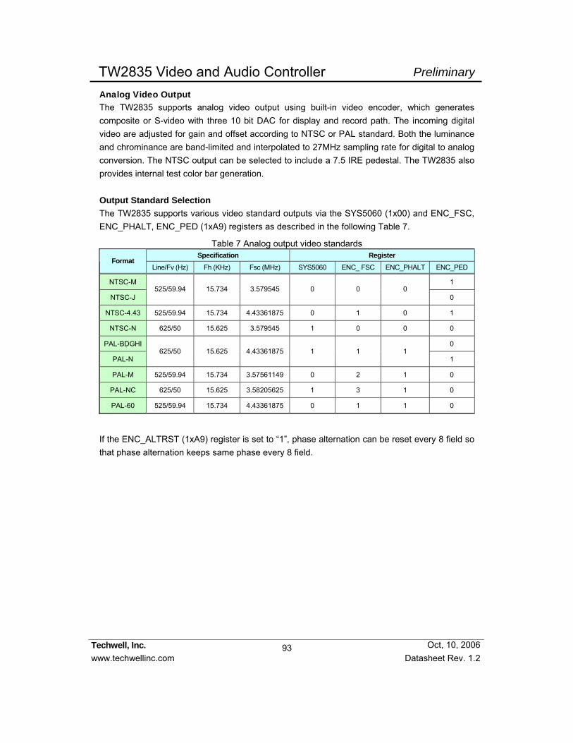
93
Techwell, Inc. www.techwellinc.com Datasheet Rev. 1.2
PreliminaryTW2835 Video and Audio Controller
Oct, 10, 2006
Analog Video Output The TW2835 supports analog video output using built-in video encoder, which generates composite or S-video with three 10 bit DAC for display and record path. The incoming digital video are adjusted for gain and offset according to NTSC or PAL standard. Both the luminance and chrominance are band-limited and interpolated to 27MHz sampling rate for digital to analog conversion. The NTSC output can be selected to include a 7.5 IRE pedestal. The TW2835 also provides internal test color bar generation. Output Standard Selection The TW2835 supports various video standard outputs via the SYS5060 (1x00) and ENC_FSC, ENC_PHALT, ENC_PED (1xA9) registers as described in the following Table 7.
Table 7 Analog output video standards Specification Register
Format Line/Fv (Hz) Fh (KHz) Fsc (MHz) SYS5060 ENC_ FSC ENC_PHALT ENC_PED
NTSC-M 1
NTSC-J 525/59.94 15.734 3.579545 0 0 0
0
NTSC-4.43 525/59.94 15.734 4.43361875 0 1 0 1
NTSC-N 625/50 15.625 3.579545 1 0 0 0
PAL-BDGHI 0
PAL-N 625/50 15.625 4.43361875 1 1 1
1
PAL-M 525/59.94 15.734 3.57561149 0 2 1 0
PAL-NC 625/50 15.625 3.58205625 1 3 1 0
PAL-60 525/59.94 15.734 4.43361875 0 1 1 0
If the ENC_ALTRST (1xA9) register is set to “1”, phase alternation can be reset every 8 field so that phase alternation keeps same phase every 8 field.

94
Techwell, Inc. www.techwellinc.com Datasheet Rev. 1.2
PreliminaryTW2835 Video and Audio Controller
Oct, 10, 2006
Luminance Filter The bandwidth of luminance signal can be selected via the YBW (1xAA) register as shown in the following Fig 62.
0 2 4 6 8 10 12
x 106
-45
-40
-35
-30
-25
-20
-15
-10
-5
0
Mag
nitu
de R
espo
nse
(dB
)
Frequency (Hertz)
Fig 62 Characteristics of luminance filter
Chrominance Filter The bandwidth of chrominance signal can be selected via the CBW (1xAA) register as shown in the following Fig 63.
0 0.5 1 1.5 2 2.5 3
x 106
-25
-20
-15
-10
-5
0
Mag
nitu
de R
espo
nse
(dB
)
Frequency (Hertz)
Fig 63 Characteristics of chrominance Filter
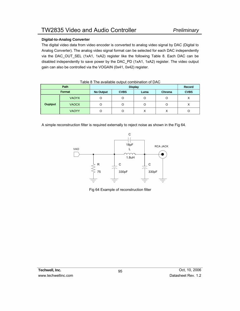
95
Techwell, Inc. www.techwellinc.com Datasheet Rev. 1.2
PreliminaryTW2835 Video and Audio Controller
Oct, 10, 2006
Digital-to-Analog Converter The digital video data from video encoder is converted to analog video signal by DAC (Digital to Analog Converter). The analog video signal format can be selected for each DAC independently via the DAC_OUT_SEL (1xA1, 1xA2) register like the following Table 8. Each DAC can be disabled independently to save power by the DAC_PD (1xA1, 1xA2) register. The video output gain can also be controlled via the VOGAIN (0x41, 0x42) register.
Table 8 The available output combination of DAC Path Display Record
Format No Output CVBS Luma Chroma CVBS
VAOYX O O O O X
VAOCX O O O O X Ouptput
VAOYY O O X X O
A simple reconstruction filter is required externally to reject noise as shown in the Fig 64.
VAORCA JACK
C
330pF
C
330pF
L
1.8uH
C
18pF
R
75
Fig 64 Example of reconstruction filter

96
Techwell, Inc. www.techwellinc.com Datasheet Rev. 1.2
PreliminaryTW2835 Video and Audio Controller
Oct, 10, 2006
Digital Video Output The digital output data of ITU-R BT.656 format is synchronized with CLKVDOX/Y pin which is 27MHz for single output or 54MHz for dual output. Each digital data of display and record path can be output through VDOX and VDOY pin respectively on single output mode. For the dual output mode, both display and record path output can come out through only one VDOX or VDOY pin. The active video level of the ITU-R BT.656 can be limited to 1 ~ 254 via the CCIR_LMT (1xA4) register. In case that channel ID is located in active video period, the CCIR_LMT should be set to low for proper digital channel ID operation.
The following Table 9 shows the ITU-R BT.656 SAV and EAV code sequence.
Table 9 ITU-R BT.656 SAV and EAV code sequence Line Condition FVH SAV/EAV Code Sequence
From To Field Vertical Horizontal F V H First Second Third Fourth
EAV 1 0xF1 523 (1*1) 3 EVEN Blank
SAV 1 1
0 0xEC
EAV 1 0xB6 4 19 ODD Blank
SAV 0 1
0 0xAB
EAV 1 0x9D 20 259
(263*1) ODD Active SAV
0 0 0 0x80
EAV 1 0xB6 260 (264*1) 265 ODD Blank
SAV 0 1
0 0xAB
EAV 1 0xF1 266 282 EVEN Blank
SAV 1 1
0 0xEC
EAV 1 0xDA
60H
z (5
25Li
nes)
283 522 (525*1) EVEN Active
SAV 1 0
0
0xFF 0x00 0x00
0xC7
EAV 1 0xB6 1 22 ODD Blank
SAV 0 1
0 0xAB
EAV 1 0x9D 23 310 ODD Active
SAV 0 0
0 0x80
EAV 1 0xB6 311 312 ODD Blank
SAV 0 1
0 0xAB
EAV 1 0xF1 313 335 EVEN Blank
SAV 1 1
0 0xEC
EAV 1 0xDA 336 623 EVEN Active
SAV 1 0
0 0xC7
EAV 1 0xF1
50H
z (6
25Li
nes)
624 625 EVEN Blank SAV
1 1 0
0xFF 0x00 0x00
0xEC
Note 1. The number of ( ) is ITU-R BT. 656 standard. The TW2835 also supports this standard by CCIR_STD register
(1xA8 Bit[6]).
The TW2835 also supports ITU-R BT.601 interface through the VDOX and VDOY pin.

97
Techwell, Inc. www.techwellinc.com Datasheet Rev. 1.2
PreliminaryTW2835 Video and Audio Controller
Oct, 10, 2006
Single Output Mode For the single output mode, each digital output data in display and record path can be output at 27MHz ITU-R BT 656 interface through VDOX and VDOY pin that are synchronized with CLKVDOX and CLKVDOY. The output data is selected by the CCIR_OUT (1xA3) register which selects the display path data for “0” and record path data for “1”. The timing diagram of single output mode for ITU-R BT.656 interface is shown in the following Fig 65.
CLKVDOX/Y
VDOX/Y[7:0] Cb0 Y0 Cr080h 10h 80h 10h FFh 00h 00h00h 00h XYFFh XY Y1
EAV code SAV code
Cb2 Y2 Cr2 Y3
Fig 65 Timing diagram of single output mode for 656 Interface
The TW2835 also supports 13.5MHz ITU-R BT 601 interface through VDOX and VDOY pin via the CCIR_601 (1xA3) register. The output data is selected via the CCIR_OUT register which chooses the display path data for “0” and record path data for “1”. The timing diagram of single output mode for ITU-R BT 601 interface is shown in the following Fig 66.
VDOX[7:0] FFh
EAV code SAV code
VDOY[7:0]
00h
00h XYh
80h
10h
80h
10h
FFh 00h
00h XYh
Cb0 Cr0
Y0 Y1
Cb2 Cr2
Y2 Y3
CLKVDOX/Y(13.5MHz)
Fig 66 Timing diagram of single output mode for 601 Interface
The video output is synchronized with CLKVDOX and CLKVDOY pins whose phase and frequency can be controlled by the ENC_CLK_FR_X, ENC_CLK_FR_Y, ENC_CLK_PH_X and ENC_CLK_PH_Y (1xAD) registers.
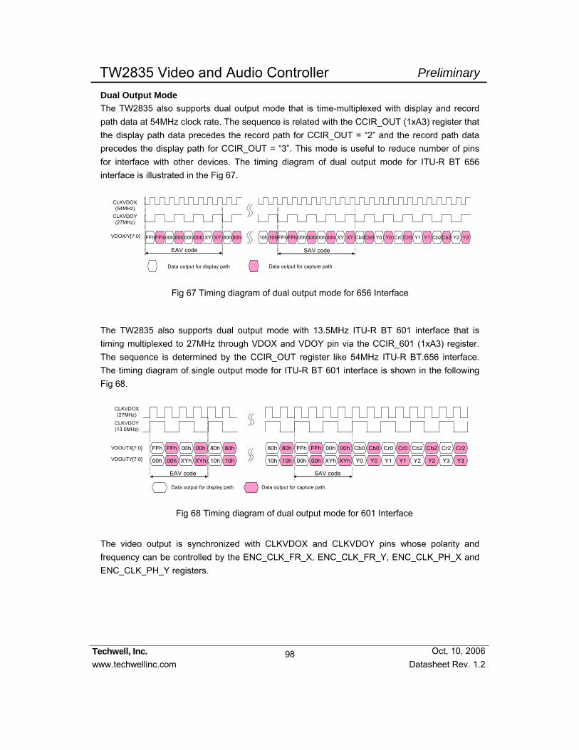
98
Techwell, Inc. www.techwellinc.com Datasheet Rev. 1.2
PreliminaryTW2835 Video and Audio Controller
Oct, 10, 2006
Dual Output Mode The TW2835 also supports dual output mode that is time-multiplexed with display and record path data at 54MHz clock rate. The sequence is related with the CCIR_OUT (1xA3) register that the display path data precedes the record path for CCIR_OUT = “2” and the record path data precedes the display path for CCIR_OUT = “3”. This mode is useful to reduce number of pins for interface with other devices. The timing diagram of dual output mode for ITU-R BT 656 interface is illustrated in the Fig 67.
CLKVDOX(54MHz)
VDOX/Y[7:0]
EAV code SAV code
FFhFFh 00h 00h 00h 00h XY XY 80h 80h 10h 10h FFhFFh 00h 00h 00h 00h XY XY Cb0Cb0 Y0 Y0 Cr0 Cr0 Y1 Y1 Cb2Cb2 Y2 Y2
CLKVDOY(27MHz)
Data output for display path Data output for capture path
Fig 67 Timing diagram of dual output mode for 656 Interface
The TW2835 also supports dual output mode with 13.5MHz ITU-R BT 601 interface that is timing multiplexed to 27MHz through VDOX and VDOY pin via the CCIR_601 (1xA3) register. The sequence is determined by the CCIR_OUT register like 54MHz ITU-R BT.656 interface. The timing diagram of single output mode for ITU-R BT 601 interface is shown in the following Fig 68.
CLKVDOX(27MHz)
VDOUTX[7:0] FFh
EAV code SAV code
VDOUTY[7:0]
FFh 00h 00h
00h 00h XYh XYh
80h 80h
10h 10h
80h 80h
10h 10h
FFh FFh 00h 00h
00h 00h XYh XYh
Cb0 Cb0 Cr0 Cr0
Y0 Y0 Y1 Y1
Cb2 Cb2 Cr2 Cr2
Y2 Y2 Y3 Y3
Data output for display path Data output for capture path
CLKVDOY(13.5MHz)
Fig 68 Timing diagram of dual output mode for 601 Interface
The video output is synchronized with CLKVDOX and CLKVDOY pins whose polarity and frequency can be controlled by the ENC_CLK_FR_X, ENC_CLK_FR_Y, ENC_CLK_PH_X and ENC_CLK_PH_Y registers.
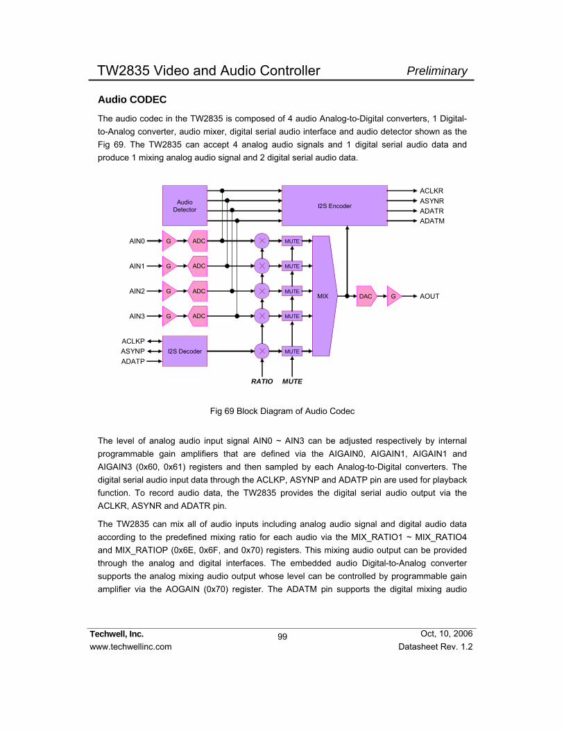
99
Techwell, Inc. www.techwellinc.com Datasheet Rev. 1.2
PreliminaryTW2835 Video and Audio Controller
Oct, 10, 2006
Audio CODEC
The audio codec in the TW2835 is composed of 4 audio Analog-to-Digital converters, 1 Digital-to-Analog converter, audio mixer, digital serial audio interface and audio detector shown as the Fig 69. The TW2835 can accept 4 analog audio signals and 1 digital serial audio data and produce 1 mixing analog audio signal and 2 digital serial audio data.
ADCAIN0 G
I2S Encoder
ACLKRASYNRADATRADATM
I2S DecoderACLKPASYNPADATP
AOUTDAC GMIX
MUTE
ADCAIN1 G MUTE
ADCAIN2 G MUTE
ADCAIN3 G MUTE
MUTE
RATIO MUTE
AudioDetector
Fig 69 Block Diagram of Audio Codec
The level of analog audio input signal AIN0 ~ AIN3 can be adjusted respectively by internal programmable gain amplifiers that are defined via the AIGAIN0, AIGAIN1, AIGAIN1 and AIGAIN3 (0x60, 0x61) registers and then sampled by each Analog-to-Digital converters. The digital serial audio input data through the ACLKP, ASYNP and ADATP pin are used for playback function. To record audio data, the TW2835 provides the digital serial audio output via the ACLKR, ASYNR and ADATR pin.
The TW2835 can mix all of audio inputs including analog audio signal and digital audio data according to the predefined mixing ratio for each audio via the MIX_RATIO1 ~ MIX_RATIO4 and MIX_RATIOP (0x6E, 0x6F, and 0x70) registers. This mixing audio output can be provided through the analog and digital interfaces. The embedded audio Digital-to-Analog converter supports the analog mixing audio output whose level can be controlled by programmable gain amplifier via the AOGAIN (0x70) register. The ADATM pin supports the digital mixing audio
100
Techwell, Inc. www.techwellinc.com Datasheet Rev. 1.2
PreliminaryTW2835 Video and Audio Controller
Oct, 10, 2006
output and its digital serial audio timings are provided through the ACLKR and ASYNR pins that are shared with the digital serial audio record timing pins.
Multi-Chip Operation The TW2835 can be operated with the cascaded connection up to 16 chips that accept 64 channel audio inputs. The Fig 70 shows the example of 16 channel audio connection using 4 chips.
Each stage chip can accept 4 analog audio signals so that four cascaded chips through the ADATP and ADATM pin will be 16 channels audio controller. The first stage chip provides 16ch digital serial audio data for record. Even though the first stage chip has only 1 digital serial audio data pin ADATR for record, the TW2835 can generate 16 channel data simultaneously using multi-channel method. Also, each stage chip can support 4 channel record outputs that are corresponding with analog audio inputs. This first stage chip can also output 16 channel mixing audio data by the digital serial audio data and analog audio signal. Each chip accepts the digital serial audio data for playback and converts it to analog signal through the Digital-to-Analog Converter.

101
Techwell, Inc. www.techwellinc.com Datasheet Rev. 1.2
PreliminaryTW2835 Video and Audio Controller
Oct, 10, 2006
TW2835First Stage
AIN1ACLKRASYNRADATRADATM
AIN2AIN3AIN4
ACLKPASYNPADATP
ALINKO
AOUT
Playback Input
TW2835Second Stage
AIN5ACLKRASYNRADATRADATM
AIN6AIN7AIN8
ACLKPASYNPADATP
ALINKO
AOUT
TW2835Third Stage
AIN9ACLKRASYNRADATRADATM
AIN10AIN11AIN12
ACLKPASYNPADATP
ALINKO
AOUT
TW2835Last Stage
AIN13ACLKRASYNRADATRADATM
AIN14AIN15AIN16
ACLKPASYNPADATP
ALINKO
AOUTAnalog Mix &Playback Output
Record Output(AIN1~AIN16)Mix Output
Record Output(AIN5~AIN16)
Record Output(AIN9~AIN16)
Record Output(AIN13~AIN16)
Analog Mix &Playback Output ALINKI
ALINKI
ALINKI
ALINKI
Analog Mix &Playback Output
Analog Mix &Playback Output
Playback Input
Playback Input
Playback Input
Fig 70 Connection for Multi-chip Operation
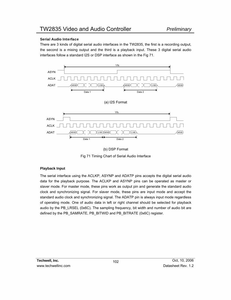
102
Techwell, Inc. www.techwellinc.com Datasheet Rev. 1.2
PreliminaryTW2835 Video and Audio Controller
Oct, 10, 2006
Serial Audio Interface There are 3 kinds of digital serial audio interfaces in the TW2835, the first is a recording output, the second is a mixing output and the third is a playback input. These 3 digital serial audio interfaces follow a standard I2S or DSP interface as shown in the Fig 71.
MSB LSB MSB LSB MSB
1/fs
ASYN
ACLK
ADAT
Data 1 Data 2
(a) I2S Format
MSB LSB MSB LSB MSB
1/fs
ASYN
ACLK
ADAT
Data 1 Data 2
(b) DSP Format
Fig 71 Timing Chart of Serial Audio Interface
Playback Input
The serial interface using the ACLKP, ASYNP and ADATP pins accepts the digital serial audio data for the playback purpose. The ACLKP and ASYNP pins can be operated as master or slaver mode. For master mode, these pins work as output pin and generate the standard audio clock and synchronizing signal. For slaver mode, these pins are input mode and accept the standard audio clock and synchronizing signal. The ADATP pin is always input mode regardless of operating mode. One of audio data in left or right channel should be selected for playback audio by the PB_LRSEL (0x6C). The sampling frequency, bit width and number of audio bit are defined by the PB_SAMRATE, PB_BITWID and PB_BITRATE (0x6C) register.

103
Techwell, Inc. www.techwellinc.com Datasheet Rev. 1.2
PreliminaryTW2835 Video and Audio Controller
Oct, 10, 2006
Record Output
To record audio data, the TW2835 provides the digital serial audio data through the ACLKR, ASYNR and ADATR pins. The RM_SAMRATE, RM_BITWID and RM_BITRATE(0x62) registers define the sampling frequency, bit width and number of audio bit. Even though the standard I2S and DSP format can have only 2 audio data on left and right channel, the TW2835 can provide an extended I2S and DSP format which can have 16 channel audio data through ADATR pin. The R_MULTCH (0x63) defines the number of audio data to be recorded by the ADATR pin. The Fig 72 shows the digital serial audio data organization for multi-channel audio.
0
1/fs
ASYNR
ACLKR
1 2 3 4 5 6 7 8 9 A B C D E F
0 1 2 3 8 9 A B
0 1 8 9
0 8
MSB LSB
8/16bit
ADATR
3
2
1
0
R_M
ULT
CH
(a) I2S Format
0
1/fs
ASYNR
ACLKR
1 2 3 4 5 6 7 8 9 A B C D E F
0
ADATR1 2 3 4 5 6 7
0 1 2 3
0 1
MSB LSB
8/16bit
3
2
1
0
R_M
ULT
CH
(b) DSP Format Fig 72 Timing Chart of Multi-channel Audio Record

104
Techwell, Inc. www.techwellinc.com Datasheet Rev. 1.2
PreliminaryTW2835 Video and Audio Controller
Oct, 10, 2006
The following Table 10 shows the sequence of audio data to be recorded for each mode of the R_MULTCH (0x63) register. The sequences of 0 ~ F do not mean actual audio channel number but represent sequence only. The actual audio channel should be assigned to sequence 0 ~ F by the R_SEQ_0 ~ R_SEQ_F (0x64 ~ 0x6B) register. When the ADATM pin is used for record via the R_ADATM (0x63) register, the audio sequence of ADATM is showed also in Table 10.
Table 10 Sequence of Multi-channel Audio Record I2S Format R_MULTCH Pin Left Channel Right Channel
ADATR 0 8 0
ADATM F 7 ADATR 0 1 8 9
1 ADATM F E 7 6 ADATR 0 1 2 3 8 9 A B
2 ADATM F E D C 7 6 5 4 ADATR 0 1 2 3 4 5 6 7 8 9 A B C D E F
3 ADATM F E D C B A 9 8 7 6 5 4 3 2 1 0
DSP Format R_MULTCH Pin Left/Right Channel
ADATR 0 1 0
ADATM F E ADATR 0 1 2 3
1 ADATM F E D C ADATR 0 1 2 3 4 5 6 7
2 ADATM F E D C B A 9 8 ADATR 0 1 2 3 4 5 6 7 8 9 A B C D E F
3 ADATM F E D C B A 9 8 7 6 5 4 3 2 1 0
Mix Output The digital serial audio data on the ADATM pin has 2 different audio data which are mixing audio and playback audio. The mixing digital serial audio data is the same as analog mixing output. The sampling frequency, bit width and number of audio for the ADATM pin are same as the ADATR pin because the ACLKR and ASYNR pins are shared with the ADATR and ADATM pins.
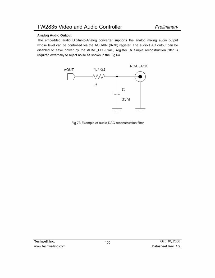
105
Techwell, Inc. www.techwellinc.com Datasheet Rev. 1.2
PreliminaryTW2835 Video and Audio Controller
Oct, 10, 2006
Analog Audio Output The embedded audio Digital-to-Analog converter supports the analog mixing audio output whose level can be controlled via the AOGAIN (0x70) register. The audio DAC output can be disabled to save power by the ADAC_PD (0x4C) register. A simple reconstruction filter is required externally to reject noise as shown in the Fig 64.
AOUTRCA JACK
C
33nF
R
4.7KΩ
Fig 73 Example of audio DAC reconstruction filter

106
Techwell, Inc. www.techwellinc.com Datasheet Rev. 1.2
PreliminaryTW2835 Video and Audio Controller
Oct, 10, 2006
Host Interface
The TW2835 provides serial and parallel interfaces that can be selected by HSPB pin. When HSPB is low, the parallel interface is selected, the serial interface for high. Some of the interface pins serve a dual purpose depending on the working mode. The pins HALE and HDAT [7] in parallel mode become SCLK and SDAT pins in serial mode and the pins HDAT [6:1] and HCSB0 in parallel mode become slave address in serial mode respectively. Each interface protocol is shown in the following figures. .
Table 11 Pin assignments for serial and parallel interface Pin Name Serial Mode Parallel Mode
HSPB HIGH LOW
HALE SCLK AEN
HRDB Not Used (VSSO) RENB
HWRB Not Used (VSSO) WENB
HCSB0 Slave Address[0] CSB0
HCSB1 Not Used (VSSO) CSB1
HDAT[0] Not Used (VSSO) PDATA[0]
HDAT[1] Slave Address[1] PDATA[1]
HDAT[2] Slave Address[2] PDATA[2]
HDAT[3] Slave Address[3] PDATA[3]
HDAT[4] Slave Address[4] PDATA[4]
HDAT[5] Slave Address[5] PDATA[5]
HDAT[6] Slave Address[6] PDATA[6]
HDAT[7] SDAT PDATA[7]

107
Techwell, Inc. www.techwellinc.com Datasheet Rev. 1.2
PreliminaryTW2835 Video and Audio Controller
Oct, 10, 2006
Serial Interface
HDAT [6:1] and HCSB0 pins define slave address in serial mode. Therefore, any slave address can be assigned for full flexibility. The Fig 74 shows an illustration of serial interface for the case of slave address (Read : “0x85”, Write : 0x84”).
SCLK
R201
4.7K
TW2835
U155
57
56
59
6061
62
636566676869
71
HSPB
HCSB1
HCSB0
HALE
HRDBHWRB
HDAT[7]
HDAT[6]HDAT[5]HDAT[4]HDAT[3]HDAT[2]HDAT[1]
HDAT[0]
3.3V/5V
R202
4.7K
R1
10K
R200
10K
3.3V/5V
Slave Address exampleRead : "10000101"Write : "10000100"
SDAT
3.3V/5V
Fig 74 The serial interface for the case of slave address. (Read : “0x85”, Write : “0x84”)
The TW2835 has total 3 pages for registers (1 page can contain 256 registers) so that the page index [1:0] is used for selecting page of registers. Page 0 is assigned for video decoder, Page 1 is for video controller / encoder and Page 2 is for OSD / motion detector / Box / Mouse pointer.
The detailed timing diagram is illustrated in the Fig 75 and Fig 76.
The TW2835 also supports automatic index increment so that it can read or write continuous multi-bytes without restart. Therefore, the host can read or write multiple bytes in sequential order without writing additional slave address, page index and index address. The data transfer rate on the bus is up to 400K bits/s.
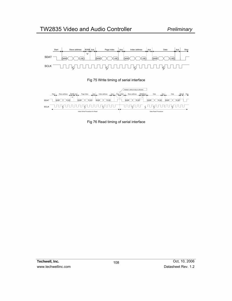
108
Techwell, Inc. www.techwellinc.com Datasheet Rev. 1.2
PreliminaryTW2835 Video and Audio Controller
Oct, 10, 2006
MSB LSB MSB LSB MSB LSB
Start Slave address R/WB Ack Page index Ack Data Ack Stop
SDAT
SCLK
MSB LSB
Index address Ack
“0”
Fig 75 Write timing of serial interface
SDAT
SCLK
MSB LSB MSB LSB
Start Slave address R/WB Ack Index address Ack
MSB LSB MSB LSB
Start Slave address R/WB Data NoAck Stop
“0” “1”
Stop
Restart without stop is allowed
Index Write Procedure for Read Data Read Procedure
MSB LSB
Page Index Ack AckAck
MSB LSB
Data
Fig 76 Read timing of serial interface
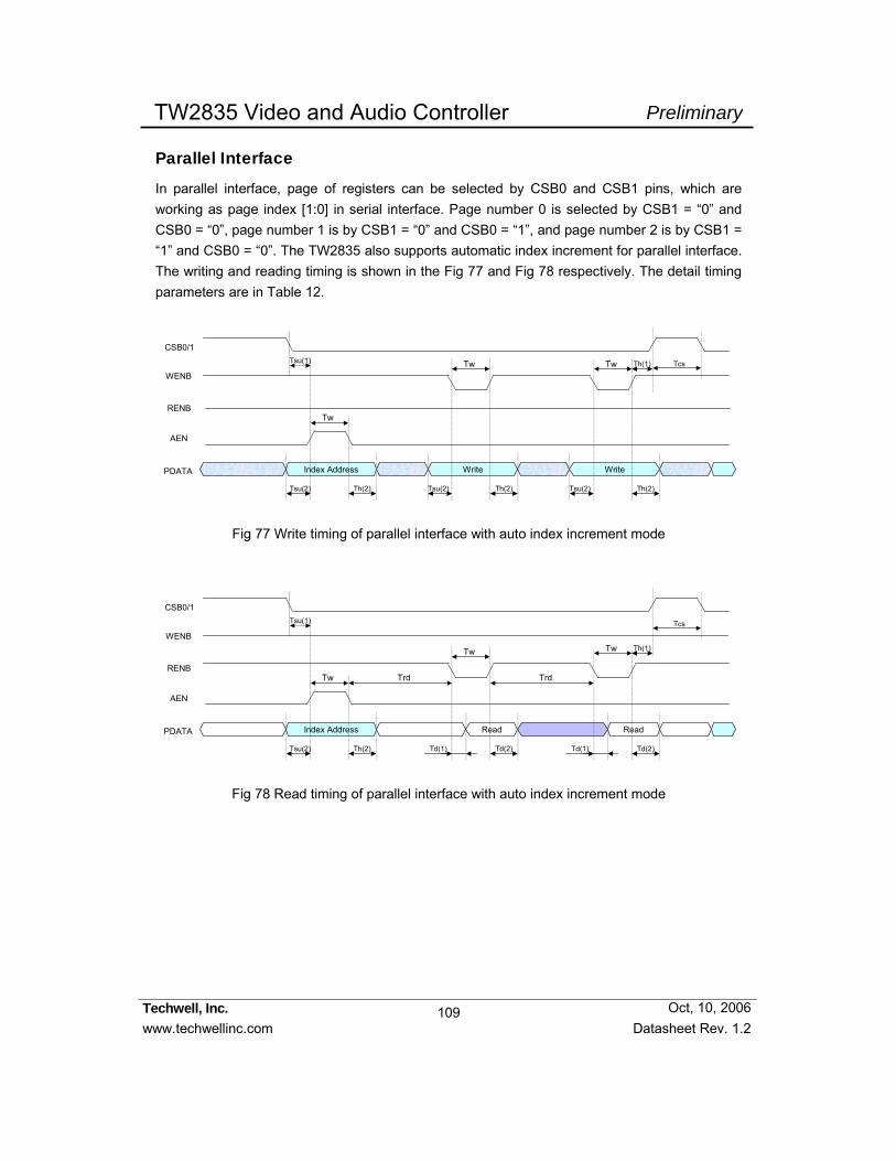
109
Techwell, Inc. www.techwellinc.com Datasheet Rev. 1.2
PreliminaryTW2835 Video and Audio Controller
Oct, 10, 2006
Parallel Interface
In parallel interface, page of registers can be selected by CSB0 and CSB1 pins, which are working as page index [1:0] in serial interface. Page number 0 is selected by CSB1 = “0” and CSB0 = “0”, page number 1 is by CSB1 = “0” and CSB0 = “1”, and page number 2 is by CSB1 = “1” and CSB0 = “0”. The TW2835 also supports automatic index increment for parallel interface. The writing and reading timing is shown in the Fig 77 and Fig 78 respectively. The detail timing parameters are in Table 12.
WriteIndex Address Write
CSB0/1
WENB
RENB
AEN
PDATA
Tsu(1) Tcs
Th(2)Tsu(2)
Tw
Tw
Tsu(2)
Tw Th(1)
Th(2) Tsu(2) Th(2)
Fig 77 Write timing of parallel interface with auto index increment mode
ReadIndex Address Read
CSB0/1
WENB
RENB
AEN
PDATA
Tsu(1) Tcs
Th(2)Tsu(2)
Tw
Tw
Td(1)
Tw Th(1)
Td(2)Td(2) Td(1)
Trd Trd
Fig 78 Read timing of parallel interface with auto index increment mode
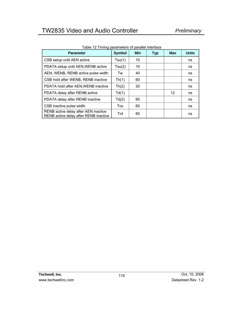
110
Techwell, Inc. www.techwellinc.com Datasheet Rev. 1.2
PreliminaryTW2835 Video and Audio Controller
Oct, 10, 2006
Table 12 Timing parameters of parallel interface Parameter Symbol Min Typ Max Units
CSB setup until AEN active Tsu(1) 10 ns
PDATA setup until AEN,WENB active Tsu(2) 10 ns
AEN, WENB, RENB active pulse width Tw 40 ns
CSB hold after WENB, RENB inactive Th(1) 60 ns
PDATA hold after AEN,WENB inactive Th(2) 20 ns
PDATA delay after RENB active Td(1) 12 ns
PDATA delay after RENB inactive Td(2) 60 ns
CSB inactive pulse width Tcs 60 ns RENB active delay after AEN inactive RENB active delay after RENB inactive Trd 60 ns

111
Techwell, Inc. www.techwellinc.com Datasheet Rev. 1.2
PreliminaryTW2835 Video and Audio Controller
Oct, 10, 2006
Interrupt Interface
The TW2835 provides the interrupt request function via an IRQ pin. Any video loss, motion, blind, and night detection will make IRQ pin high or low whose polarity can be controlled via the IRQ_POL (1x76) register. The host can distinguish what event makes interrupt request to IRQ pin by reading the status of IRQENA_NOVID (1x78), IRQENA_MD (1x79), IRQENA_BD (1x7A) and IRQENA_ND (1x7B) registers that have different function for reading and writing. For writing mode, setting “1” to those registers enables to detect the related event. For reading mode, the state of those registers has two kinds of information depending on the IRQENA_RD (1x76) register. For IRQENA_RD = “1”, the state of those registers indicates the written value on the writing mode. For IRQENA_RD = “0”, the state of those registers denotes the related event status. The interrupt request will be cleared automatically by reading those registers when the IRQENA_RD is “0”. The following Fig 79 is show an illustration of the interrupt sequence.
IRQ Pin output
IRQENA_NOVID (1x78)
IRQENA_BD (1x7A)
Clear by host read (HRDB)
00h 01h
VIN 0 video loss detect
00h
VIN 3 motion detectVIN 3 motion disappear
VIN 0 video detect
00h
VIN 3 blind detect
IRQENA_MD (1x79) 00h
08h
04h 00h
Register address 1x78h
01hRead Data
1x79h
04h
1x78h
00h
1x7Ah
08h
Event Also Cleared by read
Fig 79 the illustration of Interrupt Sequence
The TW2835 also provides the status of video loss, motion, blind and night detection for individual channel through the MPP0/1 pins with the control of the MPPSET (1xB0, 1xB1, 1xB3, 1xB5) register.

112
Techwell, Inc. www.techwellinc.com Datasheet Rev. 1.2
PreliminaryTW2835 Video and Audio Controller
Oct, 10, 2006
MPP Pin Interface
The TW2835 provides the multi-purpose pin through the DLINKI and MPP1/2 pin that is controlled via the MPP_MD, MPP_SET, MPP_DATA (1xB0 ~ 1xB5) register. But, DLINK pin is also used for cascaded interconnection in cascaded application. The following Table 13 shows the detailed mode with the control of the related register.
Table 13 MPP Pin Interface Mode MPP_MD MPP_SET I/O MPP_DATA Remark
0 In Input Data from Pin Default 1 Strobe_det_c 2 CHID_MUX[3:0] 3 CHID_MUX[7:4] 4 Mux_out_det[15:12]
Capture path
5 – 7 - Reserved 8 Strobe_det_d Display Path
9 – 13 - Reserved 14 1’b0, H, V, F BT. 656 Sync
0
15
Out
hsync, vsync, field, link Analog Encoder Sync 0 Out Write Data to Pin 1 1 In Input Data from Pin
GPP I/O Mode
0 Decoder H Sync 1 Decoder V Sync 2 Decoder Field Sync
Bit[3:0] : VIN3 ~ VIN0
3 Decoder Ch 0/1 [7:4] MSB for Ch 0/1 4 Decoder Ch 0/1 [3:0] LSB for Ch 0/1 5 Decoder Ch 2/3 [7:4] MSB for Ch 2/3 6 Decoder Ch 2/3 [3:0] LSB for Ch 2/3 7 - Reserved 8 Novid_det_m 9 Md_det_m 10 Bd_det_m 11 Nd_det_m
For VINA (ANA_SW = 0)
12 Novid_det_s 13 Md_det_s 14 Bd_det_s
2
15
Out
Nd_det_s
For VINB (ANA_SW = 1)
The TW2835 also supports four channel real-time record output using MPP1 and MPP2 pin. The video output is synchronized with CLKMPP1 and CLKMPP2 pins whose polarity and frequency can be controlled via the DEC_CLK_FR_X, DEC_CLK_FR_Y, DEC_CLK_PH_X and DEC_CLK_PH_Y registers.

PreliminaryTW2835 Video and Audio Controller
Techwell, Inc. www.techwellinc.com Datasheet Rev. 1.2
113Oct, 10, 2006
Control Register
Register Map
For Video Decoder Address
VIN0 VIN1 VIN2 VIN3 BIT7 BIT6 BIT5 BIT4 BIT3 BIT2 BIT1 BIT0
0x00 0x10 0x20 0x30 DET_FORMAT * DET_COLOR * LOCK_COLOR * LOCK_GAIN * LOCK_OFST * LOCK_HPLL * 0x01 0x11 0x21 0x31 IFMTMAN IFORMAT AGC PEDEST DET_NONSTD * DET_FLD60 * 0x02 0x12 0x22 0x32 HDELAY_XY [7:0] 0x03 0x13 0x23 0x33 HACTIVE_XY [7:0] 0x04 0x14 0x24 0x34 VDELAY_XY [7:0] 0x05 0x15 0x25 0x35 VACTIVE_XY [7:0] 0x06 0x16 0x26 0x36 0 0 VACTIVE_XY[8] VDELAY_XY[8] HACTIVE_XY [9:8] HDELAY_XY [9:8] 0x07 0x17 0x27 0x37 HUE 0x08 0x18 0x28 0x38 SAT 0x09 0x19 0x29 0x39 CONT 0x0A 0x1A 0x2A 0x3A BRT 0x0B 0x1B 0x2B 0x3B YBWI COMBMD YPEAK_MD YPEAK_GN 0x0C 0x1C 0x2C 0x3C 0 0 CKILL CTI_GN 0x0D 0x1D 0x2D 0x3D 0 0 0 0 ANA_SW SW_RESET WPEAK_MD 0x0E 0x1E 0x2E 0x3E 0 0 0 1 0 0 0 1
0x40 PB_SDEL WPEAK_REF WPEAK_RNG WPEAK_TIME 0x41 MPPCLK_OEB VOGAINCX 0 VOGAINYX 0x42 0 0 0 0 0 VOGAINYY 0x43 0 1 0 0 GNTIME OSTIME 0x44 SLICELVL HSWIDTH 0x45 FLDMODE VSMODE FLDPOL HSPOL VSPOL 1 0 0x46 IFCOMP CLPF ACCTIME APCTIME 0x47 0 1 C_CORE 0 CDEL 0x48 U_GAIN 0x49 V_GAIN 0x4A U_OFF 0x4B V_OFF 0x4C 0 0 ADAC_PD AADC_PD VADC_PD3 VADC_PD2 VADC_PD1 VADC_PD0 0x4D 0 0 0 0 NOVID_MD 1 1 0x4E 0 0 0 0 0 1 0 1 0x4F 0 0 0 0 0 0 0 0 0x50 0 0 0 0 0 0 0 0 0x51 1 0 0 0 0 0 0 0 0x52 0 0 0 0 0 1 1 0 0x53 0 0 0 0 0 0 0 0 0x54 0 0 0 0 0 0 0 0 0x55 FLD VAV 0x60 AIGAIN1 AIGAIN0

PreliminaryTW2835 Video and Audio Controller
Techwell, Inc. www.techwellinc.com Datasheet Rev. 1.2
114Oct, 10, 2006
For Video Decoder Address
VIN0 VIN1 VIN2 VIN3 BIT7 BIT6 BIT5 BIT4 BIT3 BIT2 BIT1 BIT0
0x61 AIGAIN3 AIGAIN2 0x62 M_PBSEL M_RLSWAP RM_BITRATE RM_DATMOD RM_SAMRATE RM_BITWID RM_SYNC 0x63 0 0 0 0 0 R_ADATM R_MULTCH 0x64 R_SEQ_1 R_SEQ_0 0x65 R_SEQ_3 R_SEQ_2 0x66 R_SEQ_5 R_SEQ_4 0x67 R_SEQ_7 R_SEQ_6 0x68 R_SEQ_9 R_SEQ_8 0x69 R_SEQ_B R_SEQ_A 0x6A R_SEQ_D R_SEQ_C 0x6B R_SEQ_F R_SEQ_E 0x6C 0 PB_MASTER PB_LRSEL PB_BITRATE PB_DATMOD PB_SAMRATE PB_BITWID PB_SYNC 0x6D 0 0 MIX_DERATIO MIX_MUTE 0x6E MIX_RATIO1 MIX_RATIO0 0x6F MIX_RATIO3 MIX_RATIO2 0x70 AOGAIN MIX_RATIOP 0x71 0 1 MIX_MODE MIX_OUTSEL 0x72 0 0 0 0 0 0 0 0 0x73 0 0 0 0 0 0 0 0 0x74 0 0 0 0 0 0 0 0
0x80 0x90 0xA0 0xB0 DEC_PATH_X 0 0 VSFLT_X HSFLT_X 0x81 0x91 0xA1 0xB1 VSCALE_X [15:8] 0x82 0x92 0xA2 0xB2 VSCALE_X [7:0] 0x83 0x93 0xA3 0xB3 HSCALE_X [15:8] 0x84 0x94 0xA4 0xB4 HSCALE_X [7:0] 0x85 0x95 0xA5 0xB5 0 0 0 0 VSFLT_PB HSFLT_PB 0x86 0x96 0xA6 0xB6 VSCALE_PB [15:8] 0x87 0x97 0xA7 0xB7 VSCALE_PB [7:0] 0x88 0x98 0xA8 0xB8 HSCALE_PB [15:8] 0x89 0x99 0xA9 0xB9 HSCALE_PB [7:0] 0x8A 0x9A 0xAA 0xBA 0 / 1 / 2 / 3 VSCALE_Y HSCALE_Y VSFLT_Y HSFLT_Y 0x8B 0x9B 0xAB 0xBB HDELAY_PB[7:0] 0x8C 0x9C 0xAC 0xBC HACTIVE_PB[7:0] 0x8D 0x9D 0xAD 0xBD VDELAY_PB[7:0] 0x8E 0x9E 0xAE 0xBE VACTIVE_PB[7:0] 0x8F 0x9F 0xAF 0xBF 0 0 VACTIVE_PB[8] VDELAY_PB[8] HACTIVE_PB[9:8] HDELAY_PB[9:8]
0xC0 0 PB_FLDPOL 0 0 MAN_PBCROP PB_CROP_MD PB_ACT_MD 0xC1 LIM_656_PB LIM_656_X LIM_656_Y1 LIM_656_Y0 0xC2 0 LIM_656_DEC LIM_656_Y3 LIM_656_Y2 0xC3 BGNDEN_PB BGNDCOL AUTOBGNDPB AUTOBGNDY AUTOBGNDX 0xC4 BGNDEN_Y BGNDEN_X 0xC5 PAL_DLY_Y PAL_DLY_X 0xC6 1 1 1 1 PAL_DLY_PB 0xC7 1 1 1 1 1 1 1 1

PreliminaryTW2835 Video and Audio Controller
Techwell, Inc. www.techwellinc.com Datasheet Rev. 1.2
115Oct, 10, 2006
For Video Decoder Address
VIN0 VIN1 VIN2 VIN3 BIT7 BIT6 BIT5 BIT4 BIT3 BIT2 BIT1 BIT0
0xC8 0 0 0 0 0 FLD_OFST_PB FLD_OFST_Y FLD_OFST_X 0xC9 0 0 1 1 1 1 0 0 0xCA 0 OUT_CHID 0 0 1 1 1 1 0xFE 0x28*
Notes 1. “*” stand for read only register 2. VIN0 ~ VIN3 stand for video input 0 ~ video input 3.
For Video Controller (Display path) Address
CH0 CH1 CH2 CH3 CH4 CH5 CH6 CH7 BIT7 BIT6 BIT5 BIT4 BIT3 BIT2 BIT1 BIT0
1x00 SYS_5060 OVERLAY LINK_LAST_X LINK_LAST_Y LINK_EN_X LINK_EN_Y LINK_NUM 1x01 0 0 0 TBLINK FRZ_FRAME DUAL_PAGE STRB_FLD 1x02 RECALL_FLD SAVE_FLD SAVE_HID SAVE_ADDR 1x03 SAVE_REQ 1x04 STRB_REQ 1x05 NOVID_MODE 0 0 0 AUTO_ENHACE INVALID_MODE 1x06 MUX_MODE 0 MUX_FLD 0 0 0 0 1x07 STRB_AUTO 0 0 INTR_REQX INTR_CH 1x08 MUX_OUT_CH0 MUX_OUT_CH1 1x09 MUX_OUT_CH2 MUX_OUT_CH3 1x0A CHID_MUX_OUT 1x0B ZM_EVEN_OS ZM_ODD_OS FR_EVEN_OS FR_ODD_OS 1x0C ZMENA H_ZM_MD ZMBNDCOL ZMBNDEN ZMAREAEN ZMAREA 1x0D ZOOMH 1x0E ZOOMV 1x0F FRZ_FLD BNDCOL BGDCOL BLKCOL
1x10 1x18 1x20 1x28 1x13 1x1B 1x23 1x2B CH_EN POP_UP FUNC_MODE ANA_PATH_SEL PB_PATH_EN Reserved 1x11 1x19 1x21 1x29 1x14 1x1C 1x24 1x2C RECALL_CH FRZ_CH H_MIRROR V_MIRROR ENHANCE BLANK BOUND BLINK 1x12 1x1A 1x22 1x2A 1x15 1x1D 1x25 1x2D 0 0 FIELD_OP DVR_IN RECALL_ADDR 1x16 1x1E 1x26 1x2E 1x16 1x1E 1x26 1x2E PB_AUTO_EN FLD_CONV PB_STOP EVENT_PB PB_CH_NUM 1x17 1x1F 1x27 1x2F 1x17 1x1F 1x27 1x2F 0 0 0 0 0 0 0 0 1x30 1x34 1x38 1x3C 1x40 1x44 1x48 1x4C PICHL 1x31 1x35 1x39 1x3D 1x41 1x45 1x49 1x4D PICHR 1x32 1x36 1x3A 1x3E 1x42 1x46 1x4A 1x4E PICVT 1x33 1x37 1x3B 1x3F 1x43 1x47 1x4B 1x4F PICVB Notes 1. “*” stand for read only register 2. CH0 ~ CH7 stand for channel 0 ~ channel 7.
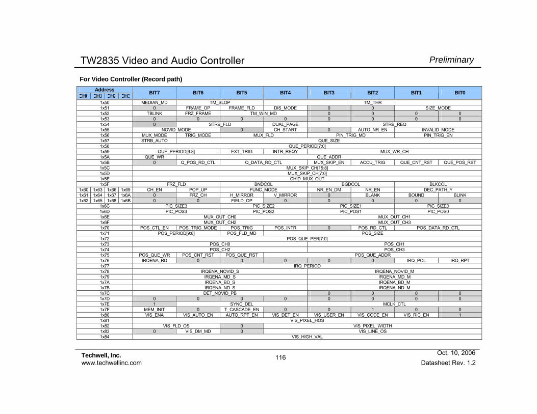
PreliminaryTW2835 Video and Audio Controller
Techwell, Inc. www.techwellinc.com Datasheet Rev. 1.2
116Oct, 10, 2006
For Video Controller (Record path) Address
CH0 CH1 CH2 CH3 BIT7 BIT6 BIT5 BIT4 BIT3 BIT2 BIT1 BIT0
1x50 MEDIAN_MD TM_SLOP TM_THR 1x51 0 FRAME_OP FRAME_FLD DIS_MODE 0 0 SIZE_MODE 1x52 TBLINK FRZ_FRAME TM_WIN_MD 0 0 0 0 1x53 0 0 0 0 0 0 0 0 1x54 0 STRB_FLD DUAL_PAGE STRB_REQ 1x55 NOVID_MODE 0 CH_START 0 AUTO_NR_EN INVALID_MODE 1x56 MUX_MODE TRIG_MODE MUX_FLD PIN_TRIG_MD PIN_TRIG_EN 1x57 STRB_AUTO QUE_SIZE 1x58 QUE_PERIOD[7:0] 1x59 QUE_PERIOD[9:8] EXT_TRIG INTR_REQY MUX_WR_CH 1x5A QUE_WR QUE_ADDR 1x5B 0 Q_POS_RD_CTL Q_DATA_RD_CTL MUX_SKIP_EN ACCU_TRIG QUE_CNT_RST QUE_POS_RST 1x5C MUX_SKIP_CH[15:8] 1x5D MUX_SKIP_CH[7:0] 1x5E CHID_MUX_OUT 1x5F FRZ_FLD BNDCOL BGDCOL BLKCOL
1x60 1x63 1x66 1x69 CH_EN POP_UP FUNC_MODE NR_EN_DM NR_EN DEC_PATH_Y 1x61 1x64 1x67 1x6A 0 FRZ_CH H_MIRROR V_MIRROR 0 BLANK BOUND BLINK 1x62 1x65 1x68 1x6B 0 0 FIELD_OP 0 0 0 0 0
1x6C PIC_SIZE3 PIC_SIZE2 PIC_SIZE1 PIC_SIZE0 1x6D PIC_POS3 PIC_POS2 PIC_POS1 PIC_POS0 1x6E MUX_OUT_CH0 MUX_OUT_CH1 1x6F MUX_OUT_CH2 MUX_OUT_CH3 1x70 POS_CTL_EN POS_TRIG_MODE POS_TRIG POS_INTR 0 POS_RD_CTL POS_DATA_RD_CTL 1x71 POS_PERIOD[9:8] POS_FLD_MD POS_SIZE 1x72 POS_QUE_PER[7:0] 1x73 POS_CH0 POS_CH1 1x74 POS_CH2 POS_CH3 1x75 POS_QUE_WR POS_CNT_RST POS_QUE_RST POS_QUE_ADDR 1x76 IRQENA_RD 0 0 0 0 0 IRQ_POL IRQ_RPT 1x77 IRQ_PERIOD 1x78 IRQENA_NOVID_S IRQENA_NOVID_M 1x79 IRQENA_MD_S IRQENA_MD_M 1x7A IRQENA_BD_S IRQENA_BD_M 1x7B IRQENA_ND_S IRQENA_ND_M 1x7C DET_NOVID_PB 0 0 0 0 1x7D 0 0 0 0 0 0 0 0 1x7E 1 SYNC_DEL MCLK_CTL 1x7F MEM_INIT 0 T_CASCADE_EN 0 0 1 0 0 1x80 VIS_ENA VIS_AUTO_EN AUTO_RPT_EN VIS_DET_EN VIS_USER_EN VIS_CODE_EN VIS_RIC_EN 1 1x81 VIS_PIXEL_HOS 1x82 VIS_FLD_OS 0 VIS_PIXEL_WIDTH 1x83 0 VIS_DM_MD 0 VIS_LINE_OS 1x84 VIS_HIGH_VAL
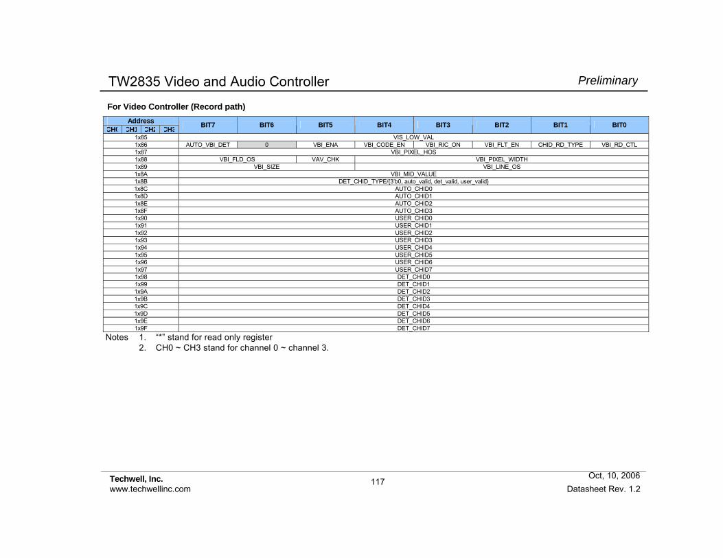
PreliminaryTW2835 Video and Audio Controller
Techwell, Inc. www.techwellinc.com Datasheet Rev. 1.2
117Oct, 10, 2006
For Video Controller (Record path) Address
CH0 CH1 CH2 CH3 BIT7 BIT6 BIT5 BIT4 BIT3 BIT2 BIT1 BIT0
1x85 VIS_LOW_VAL 1x86 AUTO_VBI_DET 0 VBI_ENA VBI_CODE_EN VBI_RIC_ON VBI_FLT_EN CHID_RD_TYPE VBI_RD_CTL 1x87 VBI_PIXEL_HOS 1x88 VBI_FLD_OS VAV_CHK VBI_PIXEL_WIDTH 1x89 VBI_SIZE VBI_LINE_OS 1x8A VBI_MID_VALUE 1x8B DET_CHID_TYPE/3’b0, auto_valid, det_valid, user_valid 1x8C AUTO_CHID0 1x8D AUTO_CHID1 1x8E AUTO_CHID2 1x8F AUTO_CHID3 1x90 USER_CHID0 1x91 USER_CHID1 1x92 USER_CHID2 1x93 USER_CHID3 1x94 USER_CHID4 1x95 USER_CHID5 1x96 USER_CHID6 1x97 USER_CHID7 1x98 DET_CHID0 1x99 DET_CHID1 1x9A DET_CHID2 1x9B DET_CHID3 1x9C DET_CHID4 1x9D DET_CHID5 1x9E DET_CHID6 1x9F DET_CHID7
Notes 1. “*” stand for read only register 2. CH0 ~ CH3 stand for channel 0 ~ channel 3.

PreliminaryTW2835 Video and Audio Controller
Techwell, Inc. www.techwellinc.com Datasheet Rev. 1.2
118Oct, 10, 2006
For Video Output
Address BIT7 BIT6 BIT5 BIT4 BIT3 BIT2 BIT1 BIT0
1xA0 ENC_IN_X ENC_IN_Y CCIR_IN_X CCIR_IN_Y 1xA1 DAC_PD_CX 0 DAC_OUT_YX DAC_PD_YX 0 DAC_OUT_CX 1xA2 1 DAC_OUT_YY DAC_PD_YY 0 0 0 1xA3 CCIR_601_X 0 CCIR_OUT_X CCIR601_Y 0 CCIR_OUT_Y 1xA4 ENC_MODE CCIR_LMT ENC_VS ENC_FLD CCIR_FLDPOL ENC_HSPOL ENC_VSPOL ENC_FLDPOL 1xA5 ENC_VSOFF ENC_VSDEL 1xA6 ENC_HSDEL[7:0] 1xA7 ENC_HSDEL[9:8] TST_FSC_FREE ACTIVE_VDEL 1xA8 ACTIVE_MD CCIR_STD ACTIVE_HDEL 1xA9 ENC_FSC 0 0 1 ENC_PHALT ENC_ALTRST ENC_PED 1xAA ENC_CBW_X ENC_YBW_X ENC_CBW_Y ENC_YBW_Y 1xAB 0 HOUT VOUT FOUT ENC_BAR_X ENC_CKILL_X ENC_BAR_Y ENC_CKILL_Y 1xAC ENC_CLK_FR_X ENC_CLK_PH_X ENC_CLK_CTL_X 1xAD ENC_CLK_FR_Y ENC_CLK_PH_Y ENC_CLK_CTL_Y 1xAE DEC_CLK_FR_X DEC_CLK_PH_X DEC_CLK_CTL_X 1xAF DEC_CLK_FR_Y DEC_CLK_PH_Y DEC_CLK_CTL_Y 1xB0 0 0 MPP_MD2 MPP_MD1 MPP_MD0 1xB1 MPP0_SET_MSB MPP0_SET_LSB 1xB2 MPP0_DATA_MSB MPP0_DATA_LSB 1xB3 MPP1_SET_MSB MPP1_SET_LSB 1xB4 MPP1_DATA_MSB MPP1_DATA_LSB 1xB5 MPP2_SET_MSB MPP2_SET_LSB 1xB6 MPP2_DATA_MSB MPP2_DATA_LSB 1xB7 MEM_INIT_DET 0 0 0 0 0 0 0 1xB8 0 1xB9 0 0 0 0 0 0 0 0 1xBA 0 0 0 0 0 0 0 0 1xBB 0 0 0 0 0 0 0 0 1xBC 0 0 0 0 0 0 0 0 1xBD 0 0 0 0 1xBE 0 0 0 0 1xBF 0 0 0 0
Notes 1. “*” stand for read only register
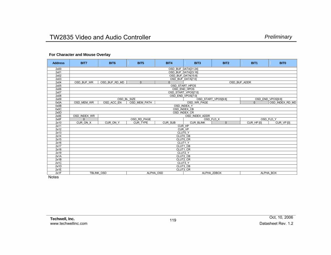
PreliminaryTW2835 Video and Audio Controller
Techwell, Inc. www.techwellinc.com Datasheet Rev. 1.2
119Oct, 10, 2006
For Character and Mouse Overlay
Address BIT7 BIT6 BIT5 BIT4 BIT3 BIT2 BIT1 BIT0
2x00 OSD_BUF_DATA[31:24] 2x01 OSD_BUF_DATA[23:16] 2x02 OSD_BUF_DATA[15:8] 2x03 OSD_BUF_DATA[7:0] 2x04 OSD_BUF_WR OSD_BUF_RD_MD 0 0 OSD_BUF_ADDR 2x05 OSD_START_HPOS 2x06 OSD_END_HPOS 2x07 OSD_START_VPOS[7:0] 2x08 OSD_END_VPOS[7:0] 2x09 OSD_BL_SIZE OSD_START_VPOS[9:8] OSD_END_VPOS[9:8] 0x0A OSD_MEM_WR OSD_ACC_EN OSD_MEM_PATH OSD_WR_PAGE 0 OSD_INDEX_RD_MD0x0B OSD_INDEX_Y 0x0C OSD_INDEX_CB 2x0D OSD_INDEX_CR 2x0E OSD_INDEX_WR OSD_INDEX_ADDR 2x0F 0 OSD_RD_PAGE OSD_FLD_X OSD_FLD_Y 2x10 CUR_ON_X CUR_ON_Y CUR_TYPE CUR_SUB CUR_BLINK 0 CUR_HP [0] CUR_VP [0] 2x11 CUR_HP 2x12 CUR_VP 2x13 CLUT0_Y 2x14 CLUT0_CB 2x15 CLUT0_CR 2x16 CLUT1_Y 2x17 CLUT1_CB 2x18 CLUT1_CR 2x19 CLUT2_Y 2x1A CLUT2_CB 2x1B CLUT2_CR 2x1C CLUT3_Y 2x1D CLUT3_CB 2x1E CLUT3_CR 2x1F TBLINK_OSD ALPHA_OSD ALPHA_2DBOX ALPHA_BOX
Notes
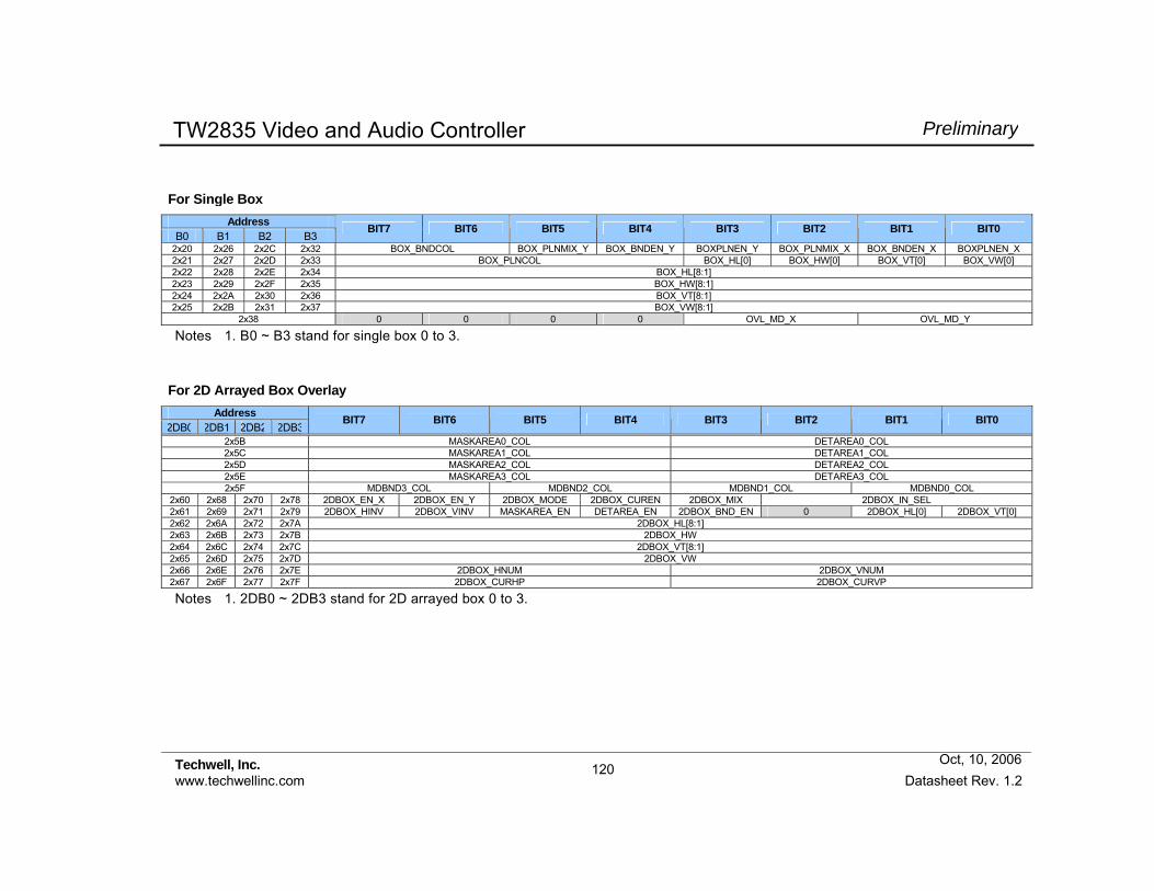
PreliminaryTW2835 Video and Audio Controller
Techwell, Inc. www.techwellinc.com Datasheet Rev. 1.2
120Oct, 10, 2006
For Single Box Address
B0 B1 B2 B3 BIT7 BIT6 BIT5 BIT4 BIT3 BIT2 BIT1 BIT0
2x20 2x26 2x2C 2x32 BOX_BNDCOL BOX_PLNMIX_Y BOX_BNDEN_Y BOXPLNEN_Y BOX_PLNMIX_X BOX_BNDEN_X BOXPLNEN_X 2x21 2x27 2x2D 2x33 BOX_PLNCOL BOX_HL[0] BOX_HW[0] BOX_VT[0] BOX_VW[0] 2x22 2x28 2x2E 2x34 BOX_HL[8:1] 2x23 2x29 2x2F 2x35 BOX_HW[8:1] 2x24 2x2A 2x30 2x36 BOX_VT[8:1] 2x25 2x2B 2x31 2x37 BOX_VW[8:1]
2x38 0 0 0 0 OVL_MD_X OVL_MD_Y
Notes 1. B0 ~ B3 stand for single box 0 to 3.
For 2D Arrayed Box Overlay Address
2DB0 2DB1 2DB2 2DB3 BIT7 BIT6 BIT5 BIT4 BIT3 BIT2 BIT1 BIT0
2x5B MASKAREA0_COL DETAREA0_COL 2x5C MASKAREA1_COL DETAREA1_COL 2x5D MASKAREA2_COL DETAREA2_COL 2x5E MASKAREA3_COL DETAREA3_COL 2x5F MDBND3_COL MDBND2_COL MDBND1_COL MDBND0_COL
2x60 2x68 2x70 2x78 2DBOX_EN_X 2DBOX_EN_Y 2DBOX_MODE 2DBOX_CUREN 2DBOX_MIX 2DBOX_IN_SEL 2x61 2x69 2x71 2x79 2DBOX_HINV 2DBOX_VINV MASKAREA_EN DETAREA_EN 2DBOX_BND_EN 0 2DBOX_HL[0] 2DBOX_VT[0] 2x62 2x6A 2x72 2x7A 2DBOX_HL[8:1] 2x63 2x6B 2x73 2x7B 2DBOX_HW 2x64 2x6C 2x74 2x7C 2DBOX_VT[8:1] 2x65 2x6D 2x75 2x7D 2DBOX_VW 2x66 2x6E 2x76 2x7E 2DBOX_HNUM 2DBOX_VNUM 2x67 2x6F 2x77 2x7F 2DBOX_CURHP 2DBOX_CURVP
Notes 1. 2DB0 ~ 2DB3 stand for 2D arrayed box 0 to 3.
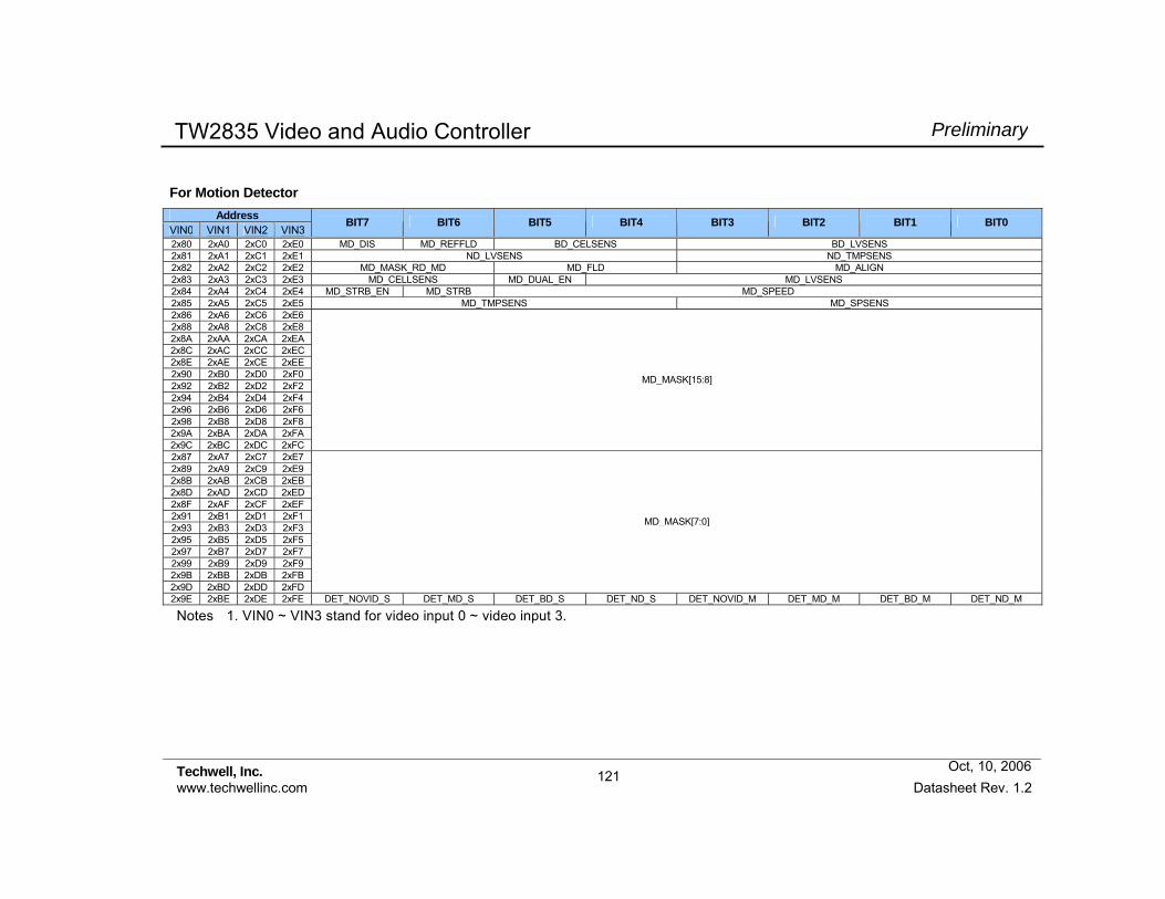
PreliminaryTW2835 Video and Audio Controller
Techwell, Inc. www.techwellinc.com Datasheet Rev. 1.2
121Oct, 10, 2006
For Motion Detector Address
VIN0 VIN1 VIN2 VIN3 BIT7 BIT6 BIT5 BIT4 BIT3 BIT2 BIT1 BIT0
2x80 2xA0 2xC0 2xE0 MD_DIS MD_REFFLD BD_CELSENS BD_LVSENS 2x81 2xA1 2xC1 2xE1 ND_LVSENS ND_TMPSENS 2x82 2xA2 2xC2 2xE2 MD_MASK_RD_MD MD_FLD MD_ALIGN 2x83 2xA3 2xC3 2xE3 MD_CELLSENS MD_DUAL_EN MD_LVSENS 2x84 2xA4 2xC4 2xE4 MD_STRB_EN MD_STRB MD_SPEED 2x85 2xA5 2xC5 2xE5 MD_TMPSENS MD_SPSENS 2x86 2xA6 2xC6 2xE6 2x88 2xA8 2xC8 2xE8 2x8A 2xAA 2xCA 2xEA 2x8C 2xAC 2xCC 2xEC 2x8E 2xAE 2xCE 2xEE 2x90 2xB0 2xD0 2xF0 2x92 2xB2 2xD2 2xF2 2x94 2xB4 2xD4 2xF4 2x96 2xB6 2xD6 2xF6 2x98 2xB8 2xD8 2xF8 2x9A 2xBA 2xDA 2xFA 2x9C 2xBC 2xDC 2xFC
MD_MASK[15:8]
2x87 2xA7 2xC7 2xE7 2x89 2xA9 2xC9 2xE9 2x8B 2xAB 2xCB 2xEB 2x8D 2xAD 2xCD 2xED 2x8F 2xAF 2xCF 2xEF 2x91 2xB1 2xD1 2xF1 2x93 2xB3 2xD3 2xF3 2x95 2xB5 2xD5 2xF5 2x97 2xB7 2xD7 2xF7 2x99 2xB9 2xD9 2xF9 2x9B 2xBB 2xDB 2xFB 2x9D 2xBD 2xDD 2xFD
MD_MASK[7:0]
2x9E 2xBE 2xDE 2xFE DET_NOVID_S DET_MD_S DET_BD_S DET_ND_S DET_NOVID_M DET_MD_M DET_BD_M DET_ND_M
Notes 1. VIN0 ~ VIN3 stand for video input 0 ~ video input 3.

122
PreliminaryTW2835 Video and Audio Controller
Techwell, Inc. www.techwellinc.com Datasheet Rev. 1.2
Oct, 10, 2006
Recommended Value For Video Decoder
Address NTSC PAL VIN0 VIN1 VIN2 VIN3 1 CH 4 CH 9 CH 16 CH 1 CH 4 CH 9 CH 16 CH 0x00 0x10 0x20 0x30 8’h00 8’h00 0x01 0x11 0x21 0x31 C8 88 0x02 0x12 0x22 0x32 20 20 0x03 0x13 0x23 0x33 D0 D0 0x04 0x14 0x24 0x34 06 05 0x05 0x15 0x25 0x35 F0 20 0x06 0x16 0x26 0x36 08 28 0x07 0x17 0x27 0x37 80 80 0x08 0x18 0x28 0x38 80 80 0x09 0x19 0x29 0x39 80 80 0x0A 0x1A 0x2A 0x3A 80 80 0x0B 0x1B 0x2B 0x3B 02 82 0x0C 0x1C 0x2C 0x3C 06 06 0x0D 0x1D 0x2D 0x3D 00 00 0x0E 0x1E 0x2E 0x3E 11 11
0x40 00 00 0x41 77 77 0x42 07 07 0x43 45 45 0x44 A0 A0 0x45 D0 D0 0x46 2F 2F 0x47 64 64 0x48 80 80 0x49 80 80 0x4A 82 82 0x4B 82 82 0x4C 00 00 0x4D 0F 0F 0x4E 05 05 0x4F 00 00 0x50 00 00 0x51 80 80 0x52 06 06 0x53 00 00 0x54 00 00 0x55 00 00 0x60 88 88 0x61 88 88 0x62 00 00 0x63 00 00 0x64 10 10 0x65 32 32 0x66 54 54 0x67 76 76 0x68 98 98

123
PreliminaryTW2835 Video and Audio Controller
Techwell, Inc. www.techwellinc.com Datasheet Rev. 1.2
Oct, 10, 2006
Address NTSC PAL VIN0 VIN1 VIN2 VIN3 1 CH 4 CH 9 CH 16 CH 1 CH 4 CH 9 CH 16 CH
0x69 BA BA 0x6A DC DC 0x6B FE FE 0x6C 00 00 0x6D 00 00 0x6E 88 88 0x6F 88 88 0x70 88 88 0x71 54 54 0x72 00 00 0x73 00 00 0x74 00 00
0x80 0x90 0xA0 0xB0 00/40/ 80/C0
01/41/ 81/C1
06/46/ 86/C6
0B/4B/ 8B/CB
00/40/ 80/C0
01/41/ 81/C1
06/46/ 86/C6
0B/4B/ 8B/CB
0x81 0x91 0xA1 0xB1 FF 7F 55 3F FF 7F 55 3F 0x82 0x92 0xA2 0xB2 FF FF 55 FF FF FF 55 FF 0x83 0x93 0xA3 0xB3 FF 7F 55 3F FF 7F 55 3F 0x84 0x94 0xA4 0xB4 FF FF 55 FF FF FF 55 FF 0x85 0x95 0xA5 0xB5 00 01 06 0B 00 01 06 0B 0x86 0x96 0xA6 0xB6 FF 7F 55 3F FF 7F 55 3F 0x87 0x97 0xA7 0xB7 FF FF 55 FF FF FF 55 FF 0x88 0x98 0xA8 0xB8 FF 7F 55 3F FF 7F 55 3F 0x89 0x99 0xA9 0xB9 FF FF 55 FF FF FF 55 FF
0x8A 0x9A 0xAA 0xBA 00/40/ 80/C0
31/71/ B1/F1 - - 00/40/
80/C0 31/71/ B1/F1 - -
0x8B 0x9B 0xAB 0xBB 00 00 0x8C 0x9C 0xAC 0xBC D0 D0 0x8D 0x9D 0xAD 0xBD 00 00 0x8E 0x9E 0xAE 0xBE F0 20 0x8F 0x9F 0xAF 0xBF 08 28
0xC0 00 00 0xC1 00 00 0xC2 00 00 0xC3 07 07 0xC4 00 00 0xC5 00 FF 00 00 00 0xC6 F0 F0 0xC7 FF FF 0xC8 00 00 0xC9 3C 3C 0xCA 0F 0F 0xFE 28 28
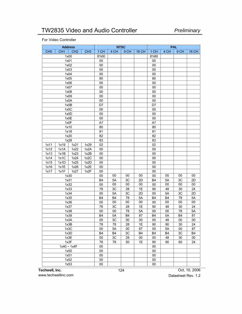
124
PreliminaryTW2835 Video and Audio Controller
Techwell, Inc. www.techwellinc.com Datasheet Rev. 1.2
Oct, 10, 2006
For Video Controller
Address NTSC PAL CH0 CH1 CH2 CH3 1 CH 4 CH 9 CH 16 CH 1 CH 4 CH 9 CH 16 CH
1x00 8’h00 8’h80 1x01 00 00 1x02 00 00 1x03 00 00 1x04 00 00 1x05 80 80 1x06 00 00 1x07 00 00 1x08 00 00 1x09 00 00 1x0A 00 00 1x0B D7 D7 1x0C 00 00 1x0D 00 00 1x0E 00 00 1x0F A7 A7 1x10 80 80 1x18 81 81 1x20 82 82 1x28 83 83
1x11 1x19 1x21 1x29 02 02 1x12 1x1A 1x22 1x2A 00 00 1x13 1x1B 1x23 1x2B 00 00 1x14 1x1C 1x24 1x2C 00 00 1x15 1x1D 1x25 1x2D 00 00 1x16 1x1E 1x26 1x2E 00 00 1x17 1x1F 1x27 1x2F 00 00
1x30 00 00 00 00 00 00 00 00 1x31 B4 5A 3C 2D B4 5A 3C 2D 1x32 00 00 00 00 00 00 00 00 1x33 78 3C 28 1E 90 48 30 24 1x34 00 5A 3C 2D 00 5A 3C 2D 1x35 B4 B4 78 5A B4 B4 78 5A 1x36 00 00 00 00 00 00 00 00 1x37 78 3C 28 1E 90 48 30 24 1x38 00 00 78 5A 00 00 78 5A 1x39 B4 5A B4 87 B4 5A B4 87 1x3A 00 3C 00 00 00 48 00 00 1x3B 78 78 28 1E 90 90 30 24 1x3C 00 5A 00 87 00 5A 00 87 1x3D B4 B4 3C B4 B4 B4 3C B4 1x3E 00 3C 28 00 00 48 30 00 1x3F 78 78 50 1E 90 90 60 24
1x40 ~ 1x4F 00 00 1x50 00 00 1x51 00 00 1x52 00 00 1x53 00 00

125
PreliminaryTW2835 Video and Audio Controller
Techwell, Inc. www.techwellinc.com Datasheet Rev. 1.2
Oct, 10, 2006
Address NTSC PAL CH0 CH1 CH2 CH3 1 CH 4 CH 9 CH 16 CH 1 CH 4 CH 9 CH 16 CH
1x54 00 00 1x55 80 80 1x56 00 00 1x57 00 00 1x58 00 00 1x59 00 00 1x5A 00 00 1x5B 00 00 1x5C 00 00 1x5D 00 00 1x5E 00 00 1x5F A7 A7 1x60 80 - - 80 - - 1x63 81 - - 81 - - 1x66 82 - - 82 - - 1x69 83 - - 83 - -
1x61 1x64 1x67 1x6A 02 - - - 1x62 1x65 1x68 1x6B 00 - - -
1x6C 00 FF - - 00 FF - - 1x6D 00 E4 - - 00 E4 - - 1x6E 00 00 1x6F 00 00 1x70 00 00 1x71 00 00 1x72 00 00 1x73 00 00 1x74 00 00 1x75 00 00 1x76 00 00 1x77 00 00 1x78 00 00 1x79 00 00 1x7A 00 00 1x7B 00 00 1x7C 00 00 1x7D 00 00 1x7E 88 88 1x7F 84 84 1x80 FF FF 1x81 00 00 1x82 51 51 1x83 07 07 1x84 EB EB 1x85 10 10 1x86 A8 A8 1x87 00 00 1x88 51 51 1x89 E7 E7 1x8A 80 80

126
PreliminaryTW2835 Video and Audio Controller
Techwell, Inc. www.techwellinc.com Datasheet Rev. 1.2
Oct, 10, 2006
Address NTSC PAL CH0 CH1 CH2 CH3 1 CH 4 CH 9 CH 16 CH 1 CH 4 CH 9 CH 16 CH
1x8B 00 00 1x8C 00 00 1x8D 00 00 1x8E 00 00 1x8F 00 00
1x90 ~ 1x9F 00 00 1xA0 77 77 1xA1 23 23 1xA2 D0 D0 1xA3 01 01 1xA4 C0 C0 1xA5 10 10 1xA6 00 00 1xA7 0D 0D 1xA8 20 20 1xA9 09 4C 1xAA AA AA 1xAB 00 00 1xAC 00 00 1xAD 00 00 1xAE 00 00 1xAF 00 00
1xB0 ~ 1xBF 00 00 Notes 1. Blanks have the same value of 1 CH. 2. All values are Hexa format.
For Motion Detector
Address VIN0 VIN1 VIN2 VIN3
NTSC PAL
2x80 2xA0 2xC0 2xE0 8’h17 8’h17 2x81 2xA1 2xC1 2xE1 88 88 2x82 2xA2 2xC2 2xE2 08 08 2x83 2xA3 2xC3 2xE3 6A 6A 2x84 2xA4 2xC4 2xE4 07 07 2x85 2xA5 2xC5 2xE5 24 24
Notes 1. All values are Hexa format.
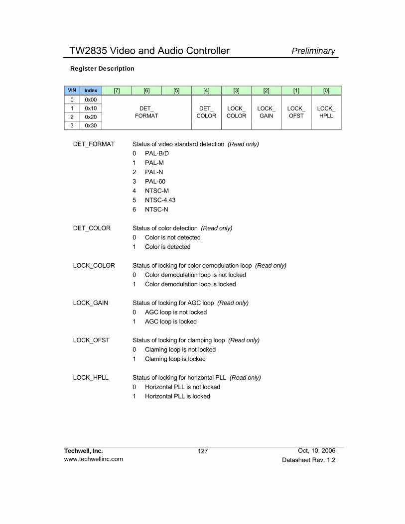
127
PreliminaryTW2835 Video and Audio Controller
Techwell, Inc. www.techwellinc.com Datasheet Rev. 1.2
Oct, 10, 2006
Register Description
VIN Index [7] [6] [5] [4] [3] [2] [1] [0] 0 0x00 1 0x10 2 0x20 3 0x30
DET_ FORMAT
DET_ COLOR
LOCK_ COLOR
LOCK_ GAIN
LOCK_ OFST
LOCK_ HPLL
DET_FORMAT Status of video standard detection (Read only) 0 PAL-B/D 1 PAL-M 2 PAL-N 3 PAL-60 4 NTSC-M 5 NTSC-4.43 6 NTSC-N DET_COLOR Status of color detection (Read only) 0 Color is not detected 1 Color is detected LOCK_COLOR Status of locking for color demodulation loop (Read only) 0 Color demodulation loop is not locked 1 Color demodulation loop is locked LOCK_GAIN Status of locking for AGC loop (Read only) 0 AGC loop is not locked 1 AGC loop is locked LOCK_OFST Status of locking for clamping loop (Read only) 0 Claming loop is not locked 1 Claming loop is locked LOCK_HPLL Status of locking for horizontal PLL (Read only) 0 Horizontal PLL is not locked 1 Horizontal PLL is locked
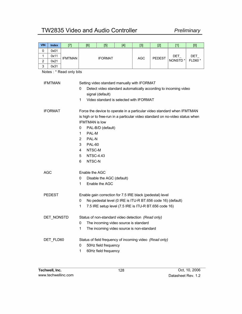
128
PreliminaryTW2835 Video and Audio Controller
Techwell, Inc. www.techwellinc.com Datasheet Rev. 1.2
Oct, 10, 2006
VIN Index [7] [6] [5] [4] [3] [2] [1] [0] 0 0x01 1 0x11 2 0x21 3 0x31
IFMTMAN IFORMAT AGC PEDEST DET_ NONSTD *
DET_ FLD60 *
Notes : * Read only bits IFMTMAN Setting video standard manually with IFORMAT 0 Detect video standard automatically according to incoming video signal (default) 1 Video standard is selected with IFORMAT IFORMAT Force the device to operate in a particular video standard when IFMTMAN is high or to free-run in a particular video standard on no-video status when IFMTMAN is low 0 PAL-B/D (default) 1 PAL-M 2 PAL-N 3 PAL-60 4 NTSC-M 5 NTSC-4.43 6 NTSC-N AGC Enable the AGC 0 Disable the AGC (default) 1 Enable the AGC PEDEST Enable gain correction for 7.5 IRE black (pedestal) level 0 No pedestal level (0 IRE is ITU-R BT.656 code 16) (default) 1 7.5 IRE setup level (7.5 IRE is ITU-R BT.656 code 16) DET_NONSTD Status of non-standard video detection (Read only) 0 The incoming video source is standard 1 The incoming video source is non-standard DET_FLD60 Status of field frequency of incoming video (Read only) 0 50Hz field frequency 1 60Hz field frequency

129
PreliminaryTW2835 Video and Audio Controller
Techwell, Inc. www.techwellinc.com Datasheet Rev. 1.2
Oct, 10, 2006
VIN Index [7] [6] [5] [4] [3] [2] [1] [0] 0 0x06 1 0x16 2 0x26 3 0x36
0 0 VACTIVE_XY[8]
VDELAY_XY[8] HACITIVE_XY[9:8] HDELAY_XY[9:8]
0 0x02 1 0x12 2 0x22 3 0x32
HDELAY_XY[7:0]
HDELAY_XY This 10bit register defines the starting location of horizontal active pixel for
display / record path. A unit is 1 pixel. The default value is decimal 32.
VIN Index [7] [6] [5] [4] [3] [2] [1] [0] 0 0x06 1 0x16 2 0x26 3 0x36
0 0 VACTIVE_XY[8]
VDELAY_XY[8]
HACITIVE_XY[9:8] HDELAY_XY[9:8]
0 0x03 1 0x13 2 0x23 3 0x33
HACTIVE_XY[7:0]
HACTIVE_XY This 10bit register defines the number of horizontal active pixel for display /
record path. A unit is 1 pixel. The default value is decimal 720.

130
PreliminaryTW2835 Video and Audio Controller
Techwell, Inc. www.techwellinc.com Datasheet Rev. 1.2
Oct, 10, 2006
VIN Index [7] [6] [5] [4] [3] [2] [1] [0] 0 0x06 1 0x16 2 0x26 3 0x36
0 0 VACTIVE_XY[8]
VDELAY_XY[8] HACITIVE_XY[9:8] HDELAY_XY[9:8]
0 0x04 1 0x14 2 0x24 3 0x34
VDELAY_XY[7:0]
VDELAY_XY This 9bit register defines the starting location of vertical active for display /
record path. A unit is 1 line. The default value is decimal 6.
VIN Index [7] [6] [5] [4] [3] [2] [1] [0] 0 0x06 1 0x16 2 0x26 3 0x36
0 0 VACTIVE_XY[8]
VDELAY_XY[8]
HACITIVE_XY[9:8] HDELAY_XY[9:8]
0 0x05 1 0x15 2 0x25 3 0x35
VACTIVE_XY[7:0]
VACTIVE_XY This 9bit register defines the number of vertical active lines for display /
record path. A unit is 1 line. The default value is decimal 240.
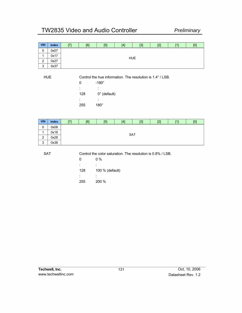
131
PreliminaryTW2835 Video and Audio Controller
Techwell, Inc. www.techwellinc.com Datasheet Rev. 1.2
Oct, 10, 2006
VIN Index [7] [6] [5] [4] [3] [2] [1] [0] 0 0x07 1 0x17 2 0x27 3 0x37
HUE
HUE Control the hue information. The resolution is 1.4° / LSB. 0 -180° : : 128 0° (default) : : 255 180°
VIN Index [7] [6] [5] [4] [3] [2] [1] [0] 0 0x08 1 0x18 2 0x28 3 0x38
SAT
SAT Control the color saturation. The resolution is 0.8% / LSB. 0 0 % : : 128 100 % (default) : : 255 200 %
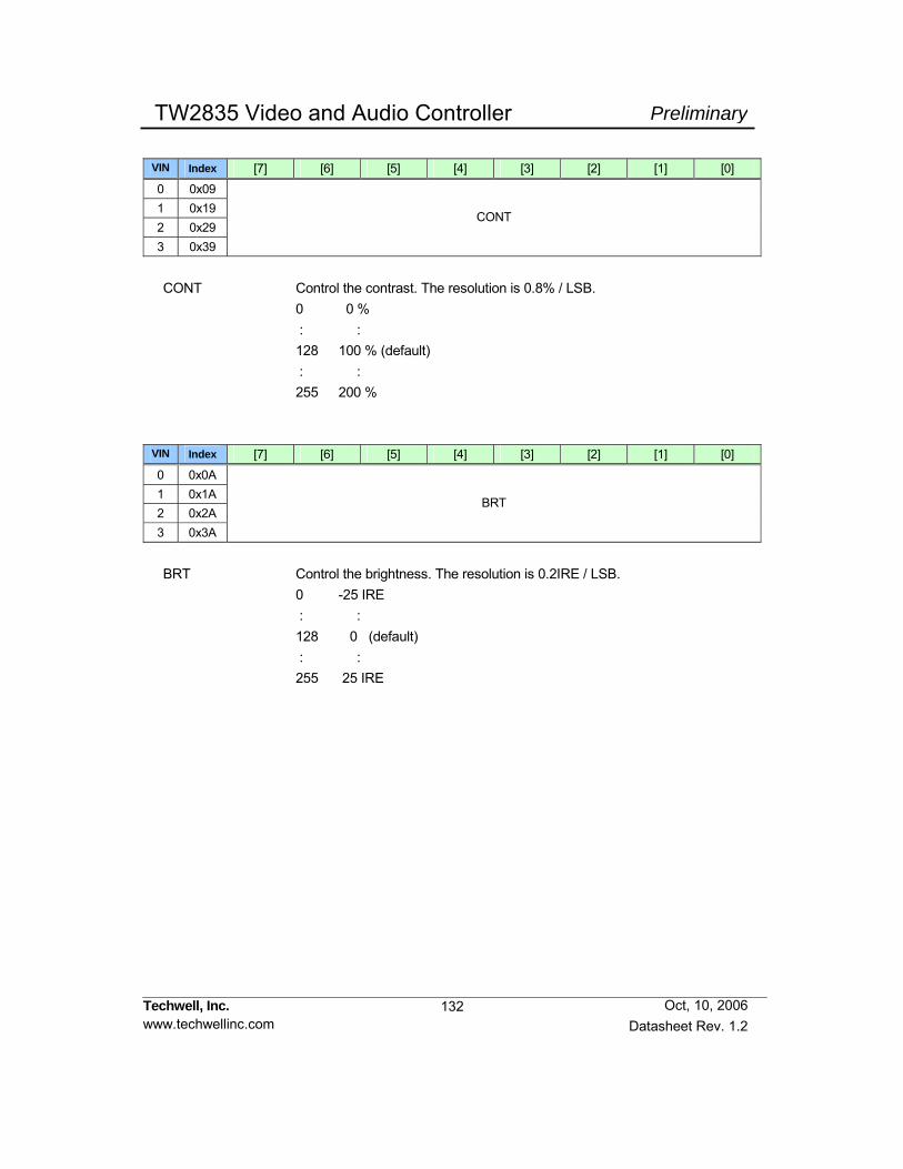
132
PreliminaryTW2835 Video and Audio Controller
Techwell, Inc. www.techwellinc.com Datasheet Rev. 1.2
Oct, 10, 2006
VIN Index [7] [6] [5] [4] [3] [2] [1] [0] 0 0x09 1 0x19 2 0x29 3 0x39
CONT
CONT Control the contrast. The resolution is 0.8% / LSB. 0 0 % : : 128 100 % (default) : : 255 200 %
VIN Index [7] [6] [5] [4] [3] [2] [1] [0] 0 0x0A 1 0x1A 2 0x2A 3 0x3A
BRT
BRT Control the brightness. The resolution is 0.2IRE / LSB. 0 -25 IRE : : 128 0 (default) : : 255 25 IRE

133
PreliminaryTW2835 Video and Audio Controller
Techwell, Inc. www.techwellinc.com Datasheet Rev. 1.2
Oct, 10, 2006
VIN Index [7] [6] [5] [4] [3] [2] [1] [0] 0 0x0B 1 0x1B 2 0x2B 3 0x3B
YBWI COMBMD YPEAK_ MD YPEAK_GN
YBWI Select the luminance trap filter mode 0 Narrow bandwidth trap filter mode (default) 1 Wide bandwidth trap filter mode COMBMD Select the adaptive comb filter mode 0,1 Adaptive comb filter mode (default) 2 Force trap filter mode 3 Not supported YPEAK_MD Select the luminance peaking frequency band 0 4~5 MHz frequency band (default) 1 2~4 MHz frequency band YPEAK_GN Control the luminance peaking gain 0 No peaking (default) 1 12.5 % 2 25 % 3 37.5 % 4 50 % 5 62.5 % 6 75 % 7 87.5 % 8 100 % 9 112.5 % 10 125 % 11 137.5 % 12 150 % 13 162.5 % 14 175 % 15 187.5 %

134
PreliminaryTW2835 Video and Audio Controller
Techwell, Inc. www.techwellinc.com Datasheet Rev. 1.2
Oct, 10, 2006
VIN Index [7] [6] [5] [4] [3] [2] [1] [0] 0 0x0C 1 0x1C 2 0x2C 3 0x3C
0 0 CKILL CTI_GN
CKIL Control the color killing mode 0,1 Auto detection mode (default) 2 Color is always alive 3 Color is always killed CTI_GN Control the CTI gain 0 No CTI 1 12.5 % 2 25 % 3 37.5 % 4 50 % 5 62.5 % 6 75 % (default) 7 87.5 % 8 100 % 9 112.5 % 10 125 % 11 137.5 % 12 150 % 13 162.5 % 14 175 % 15 187.5 %
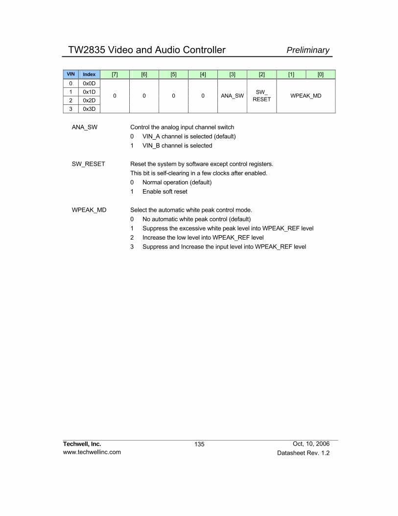
135
PreliminaryTW2835 Video and Audio Controller
Techwell, Inc. www.techwellinc.com Datasheet Rev. 1.2
Oct, 10, 2006
VIN Index [7] [6] [5] [4] [3] [2] [1] [0] 0 0x0D 1 0x1D 2 0x2D 3 0x3D
0 0 0 0 ANA_SW SW_ RESET WPEAK_MD
ANA_SW Control the analog input channel switch 0 VIN_A channel is selected (default) 1 VIN_B channel is selected SW_RESET Reset the system by software except control registers. This bit is self-clearing in a few clocks after enabled. 0 Normal operation (default) 1 Enable soft reset WPEAK_MD Select the automatic white peak control mode. 0 No automatic white peak control (default) 1 Suppress the excessive white peak level into WPEAK_REF level 2 Increase the low level into WPEAK_REF level 3 Suppress and Increase the input level into WPEAK_REF level
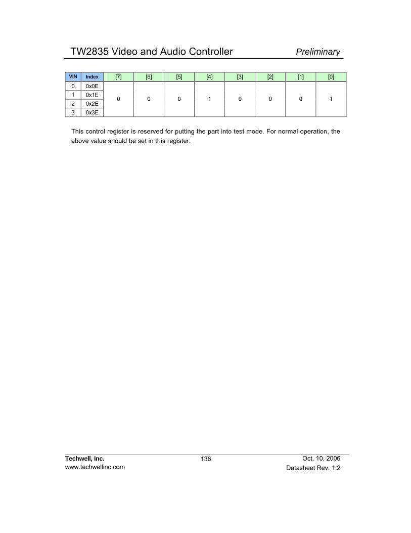
136
PreliminaryTW2835 Video and Audio Controller
Techwell, Inc. www.techwellinc.com Datasheet Rev. 1.2
Oct, 10, 2006
VIN Index [7] [6] [5] [4] [3] [2] [1] [0] 0 0x0E 1 0x1E 2 0x2E 3 0x3E
0 0 0 1 0 0 0 1
This control register is reserved for putting the part into test mode. For normal operation, the above value should be set in this register.
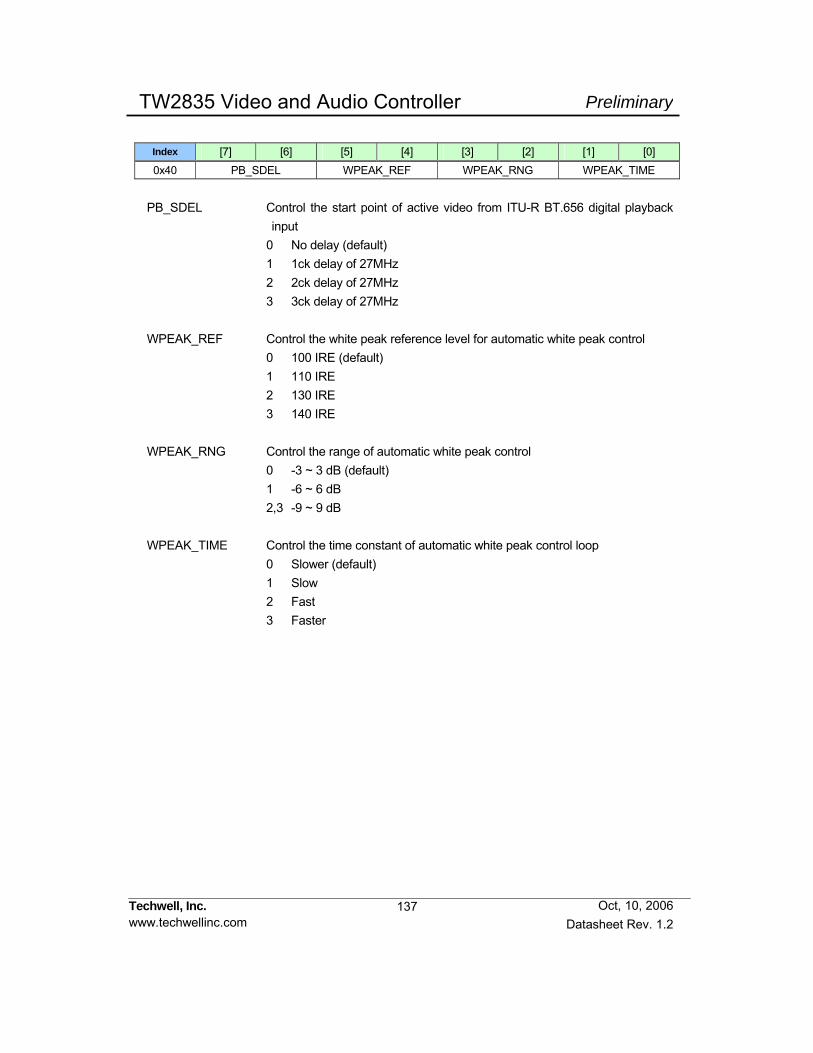
137
PreliminaryTW2835 Video and Audio Controller
Techwell, Inc. www.techwellinc.com Datasheet Rev. 1.2
Oct, 10, 2006
Index [7] [6] [5] [4] [3] [2] [1] [0] 0x40 PB_SDEL WPEAK_REF WPEAK_RNG WPEAK_TIME
PB_SDEL Control the start point of active video from ITU-R BT.656 digital playback
input 0 No delay (default) 1 1ck delay of 27MHz 2 2ck delay of 27MHz 3 3ck delay of 27MHz WPEAK_REF Control the white peak reference level for automatic white peak control 0 100 IRE (default) 1 110 IRE 2 130 IRE 3 140 IRE WPEAK_RNG Control the range of automatic white peak control 0 -3 ~ 3 dB (default) 1 -6 ~ 6 dB 2,3 -9 ~ 9 dB WPEAK_TIME Control the time constant of automatic white peak control loop 0 Slower (default) 1 Slow 2 Fast 3 Faster
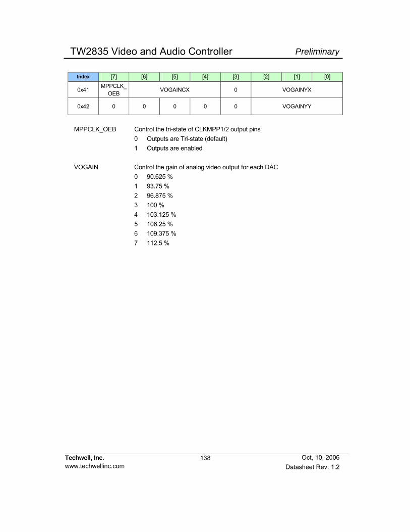
138
PreliminaryTW2835 Video and Audio Controller
Techwell, Inc. www.techwellinc.com Datasheet Rev. 1.2
Oct, 10, 2006
Index [7] [6] [5] [4] [3] [2] [1] [0]
0x41 MPPCLK_
OEB VOGAINCX 0 VOGAINYX
0x42 0 0 0 0 0 VOGAINYY
MPPCLK_OEB Control the tri-state of CLKMPP1/2 output pins 0 Outputs are Tri-state (default) 1 Outputs are enabled VOGAIN Control the gain of analog video output for each DAC 0 90.625 % 1 93.75 % 2 96.875 % 3 100 % 4 103.125 % 5 106.25 % 6 109.375 % 7 112.5 %
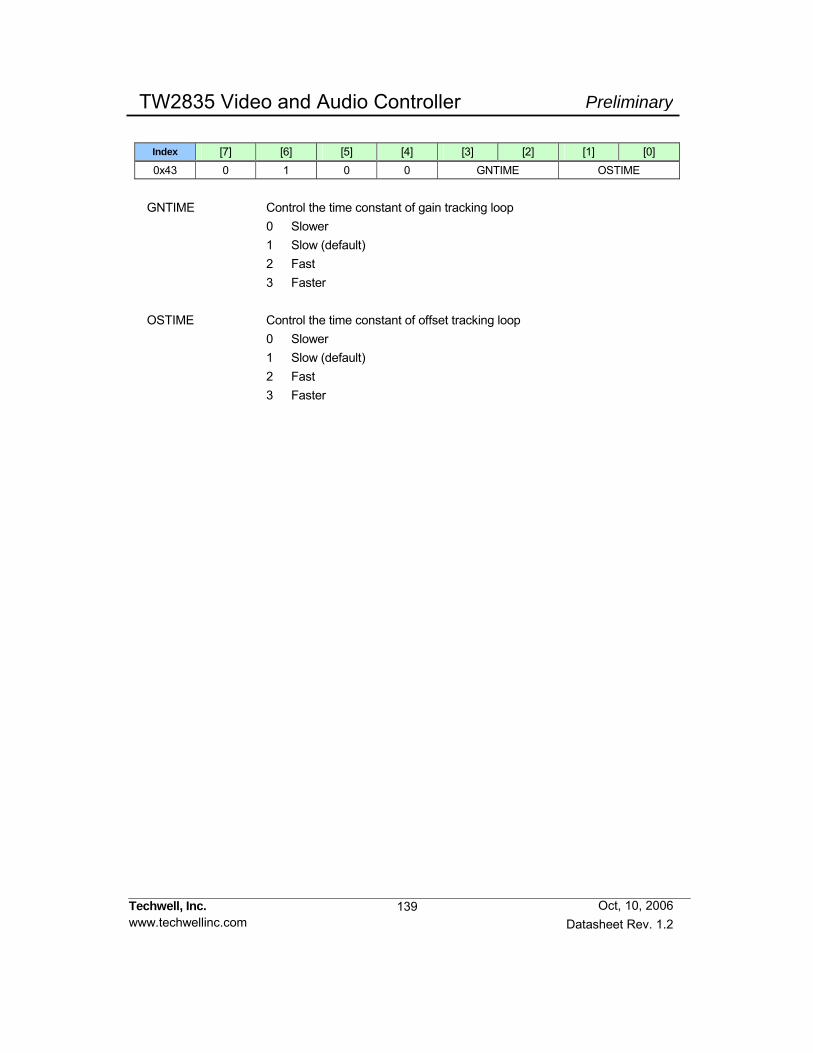
139
PreliminaryTW2835 Video and Audio Controller
Techwell, Inc. www.techwellinc.com Datasheet Rev. 1.2
Oct, 10, 2006
Index [7] [6] [5] [4] [3] [2] [1] [0] 0x43 0 1 0 0 GNTIME OSTIME
GNTIME Control the time constant of gain tracking loop 0 Slower 1 Slow (default) 2 Fast 3 Faster OSTIME Control the time constant of offset tracking loop 0 Slower 1 Slow (default) 2 Fast 3 Faster
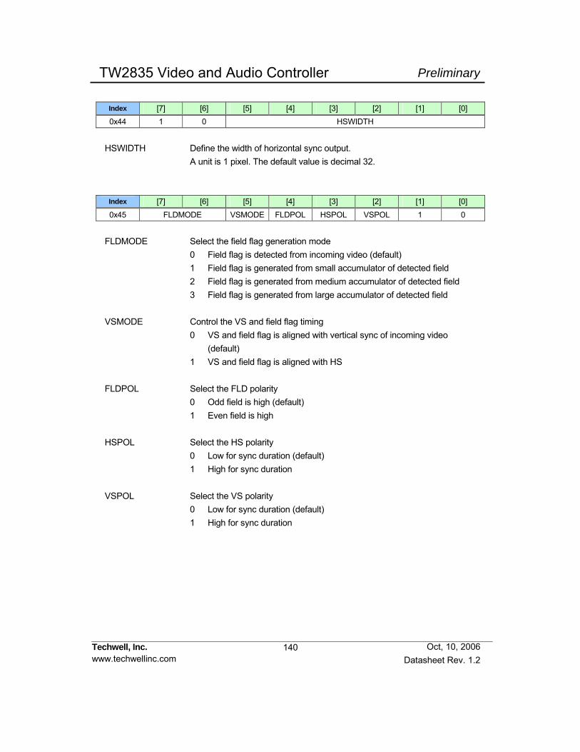
140
PreliminaryTW2835 Video and Audio Controller
Techwell, Inc. www.techwellinc.com Datasheet Rev. 1.2
Oct, 10, 2006
Index [7] [6] [5] [4] [3] [2] [1] [0] 0x44 1 0 HSWIDTH
HSWIDTH Define the width of horizontal sync output. A unit is 1 pixel. The default value is decimal 32.
Index [7] [6] [5] [4] [3] [2] [1] [0] 0x45 FLDMODE VSMODE FLDPOL HSPOL VSPOL 1 0
FLDMODE Select the field flag generation mode 0 Field flag is detected from incoming video (default) 1 Field flag is generated from small accumulator of detected field 2 Field flag is generated from medium accumulator of detected field 3 Field flag is generated from large accumulator of detected field VSMODE Control the VS and field flag timing 0 VS and field flag is aligned with vertical sync of incoming video (default) 1 VS and field flag is aligned with HS FLDPOL Select the FLD polarity 0 Odd field is high (default) 1 Even field is high HSPOL Select the HS polarity 0 Low for sync duration (default) 1 High for sync duration VSPOL Select the VS polarity 0 Low for sync duration (default) 1 High for sync duration
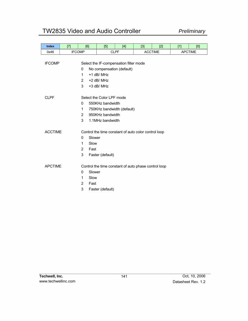
141
PreliminaryTW2835 Video and Audio Controller
Techwell, Inc. www.techwellinc.com Datasheet Rev. 1.2
Oct, 10, 2006
Index [7] [6] [5] [4] [3] [2] [1] [0] 0x46 IFCOMP CLPF ACCTIME APCTIME
IFCOMP Select the IF-compensation filter mode 0 No compensation (default) 1 +1 dB/ MHz 2 +2 dB/ MHz 3 +3 dB/ MHz CLPF Select the Color LPF mode 0 550KHz bandwidth 1 750KHz bandwidth (default) 2 950KHz bandwidth 3 1.1MHz bandwidth ACCTIME Control the time constant of auto color control loop 0 Slower 1 Slow 2 Fast 3 Faster (default) APCTIME Control the time constant of auto phase control loop 0 Slower 1 Slow 2 Fast 3 Faster (default)
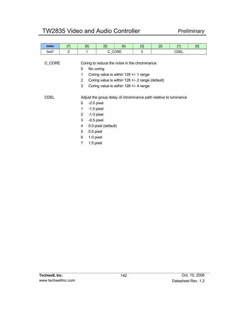
142
PreliminaryTW2835 Video and Audio Controller
Techwell, Inc. www.techwellinc.com Datasheet Rev. 1.2
Oct, 10, 2006
Index [7] [6] [5] [4] [3] [2] [1] [0] 0x47 0 1 C_CORE 0 CDEL
C_CORE Coring to reduce the noise in the chrominance 0 No coring 1 Coring value is within 128 +/- 1 range 2 Coring value is within 128 +/- 2 range (default) 3 Coring value is within 128 +/- 4 range CDEL Adjust the group delay of chrominance path relative to luminance 0 -2.0 pixel 1 -1.5 pixel 2 -1.0 pixel 3 -0.5 pixel 4 0.0 pixel (default) 5 0.5 pixel 6 1.0 pixel 7 1.5 pixel
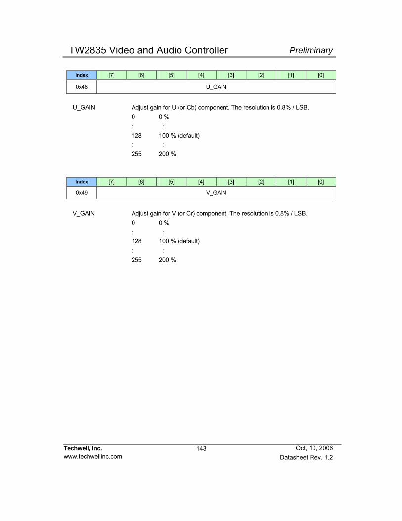
143
PreliminaryTW2835 Video and Audio Controller
Techwell, Inc. www.techwellinc.com Datasheet Rev. 1.2
Oct, 10, 2006
Index [7] [6] [5] [4] [3] [2] [1] [0]
0x48 U_GAIN
U_GAIN Adjust gain for U (or Cb) component. The resolution is 0.8% / LSB. 0 0 % : : 128 100 % (default) : : 255 200 %
Index [7] [6] [5] [4] [3] [2] [1] [0]
0x49 V_GAIN
V_GAIN Adjust gain for V (or Cr) component. The resolution is 0.8% / LSB. 0 0 % : : 128 100 % (default) : : 255 200 %
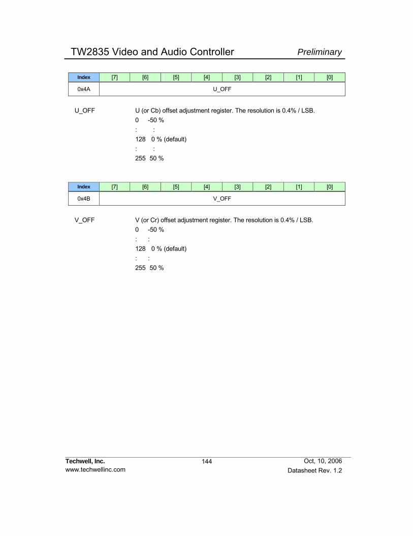
144
PreliminaryTW2835 Video and Audio Controller
Techwell, Inc. www.techwellinc.com Datasheet Rev. 1.2
Oct, 10, 2006
Index [7] [6] [5] [4] [3] [2] [1] [0]
0x4A U_OFF
U_OFF U (or Cb) offset adjustment register. The resolution is 0.4% / LSB. 0 -50 % : : 128 0 % (default) : : 255 50 % Index [7] [6] [5] [4] [3] [2] [1] [0]
0x4B V_OFF
V_OFF V (or Cr) offset adjustment register. The resolution is 0.4% / LSB. 0 -50 % : : 128 0 % (default) : : 255 50 %

145
PreliminaryTW2835 Video and Audio Controller
Techwell, Inc. www.techwellinc.com Datasheet Rev. 1.2
Oct, 10, 2006
Index [7] [6] [5] [4] [3] [2] [1] [0]
0x4C 0 0 ADAC_
PD AADC_
PD VADC_PD
ADAC_PD Power down the audio DAC. 0 Normal operation (default) 1 Power down AADC_PD Power down the audio ADC. 0 Normal operation (default) 1 Power down VADC_PD Power down the video ADC. VADC_PD[3:0] stands for CH3 to CH0. 0 Normal operation (default) 1 Power down
Index [7] [6] [5] [4] [3] [2] [1] [0] 0x4D 0 0 0 0 NOVID_MD 1 1
NOVID_MD Select the No-video flag generation mode 0 Faster 1 Fast 2 Slow 3 Slower (default)

146
PreliminaryTW2835 Video and Audio Controller
Techwell, Inc. www.techwellinc.com Datasheet Rev. 1.2
Oct, 10, 2006
Index [7] [6] [5] [4] [3] [2] [1] [0] 0x4E 0 0 0 0 0 1 0 1 0x4F 0 0 0 0 0 0 0 0 0x50 0 0 0 0 0 0 0 0 0x51 1 0 0 0 0 0 0 0 0x52 0 0 0 0 0 1 1 0 0x53 0 0 0 0 0 0 0 0 0x54 0 0 0 0 0 0 0 0
This control register is reserved for putting the part into test mode. For normal operation, the above value should be set in this register.
Index [7] [6] [5] [4] [3] [2] [1] [0] 0x55 FLD VAV
FLD Status of the field flag for corresponding channel (Read only) FLD[3:0] stands for VIN3 to VIN0. 0 Odd field when FLDPOL (0x46) = 1 1 Even field when FLDPOL (0x46) = 1 VAV Status of the vertical active video signal for corresponding channel (Read only). VAV[3:0] stands for VIN3 to VIN0. 0 Vertical blanking time 1 Vertical active time
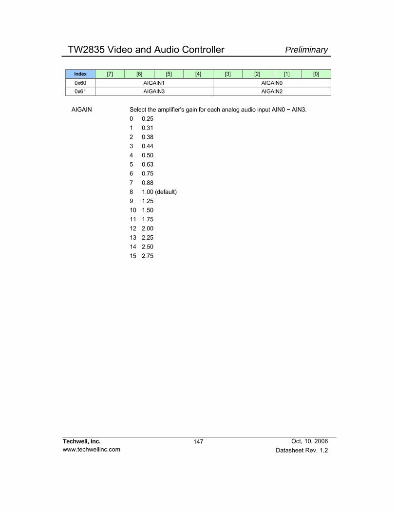
147
PreliminaryTW2835 Video and Audio Controller
Techwell, Inc. www.techwellinc.com Datasheet Rev. 1.2
Oct, 10, 2006
Index [7] [6] [5] [4] [3] [2] [1] [0] 0x60 AIGAIN1 AIGAIN0 0x61 AIGAIN3 AIGAIN2
AIGAIN Select the amplifier’s gain for each analog audio input AIN0 ~ AIN3. 0 0.25 1 0.31 2 0.38 3 0.44 4 0.50 5 0.63 6 0.75 7 0.88 8 1.00 (default) 9 1.25 10 1.50 11 1.75 12 2.00 13 2.25 14 2.50 15 2.75
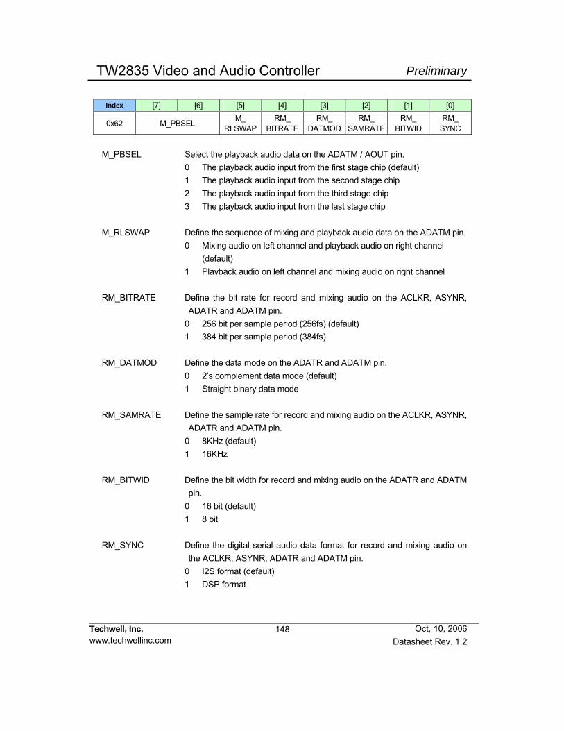
148
PreliminaryTW2835 Video and Audio Controller
Techwell, Inc. www.techwellinc.com Datasheet Rev. 1.2
Oct, 10, 2006
Index [7] [6] [5] [4] [3] [2] [1] [0]
0x62 M_PBSEL M_
RLSWAP RM_
BITRATE RM_
DATMODRM_
SAMRATERM_
BITWID RM_
SYNC
M_PBSEL Select the playback audio data on the ADATM / AOUT pin. 0 The playback audio input from the first stage chip (default) 1 The playback audio input from the second stage chip 2 The playback audio input from the third stage chip 3 The playback audio input from the last stage chip M_RLSWAP Define the sequence of mixing and playback audio data on the ADATM pin. 0 Mixing audio on left channel and playback audio on right channel (default) 1 Playback audio on left channel and mixing audio on right channel RM_BITRATE Define the bit rate for record and mixing audio on the ACLKR, ASYNR,
ADATR and ADATM pin. 0 256 bit per sample period (256fs) (default) 1 384 bit per sample period (384fs) RM_DATMOD Define the data mode on the ADATR and ADATM pin. 0 2’s complement data mode (default) 1 Straight binary data mode RM_SAMRATE Define the sample rate for record and mixing audio on the ACLKR, ASYNR,
ADATR and ADATM pin. 0 8KHz (default) 1 16KHz RM_BITWID Define the bit width for record and mixing audio on the ADATR and ADATM
pin. 0 16 bit (default) 1 8 bit RM_SYNC Define the digital serial audio data format for record and mixing audio on
the ACLKR, ASYNR, ADATR and ADATM pin. 0 I2S format (default) 1 DSP format

149
PreliminaryTW2835 Video and Audio Controller
Techwell, Inc. www.techwellinc.com Datasheet Rev. 1.2
Oct, 10, 2006
Index [7] [6] [5] [4] [3] [2] [1] [0] 0x63 0 0 0 0 0 R_ADATM R_MULTCH
R_ADATM Select the output mode for the ADATM pin. 0 Digital serial data of mixing audio (default) 1 Digital serial data of record audio R_MULTCH Define the number of audio for record on the ADATR pin. 0 2 audios (default) 1 4 audios 2 8 audios 3 16 audios
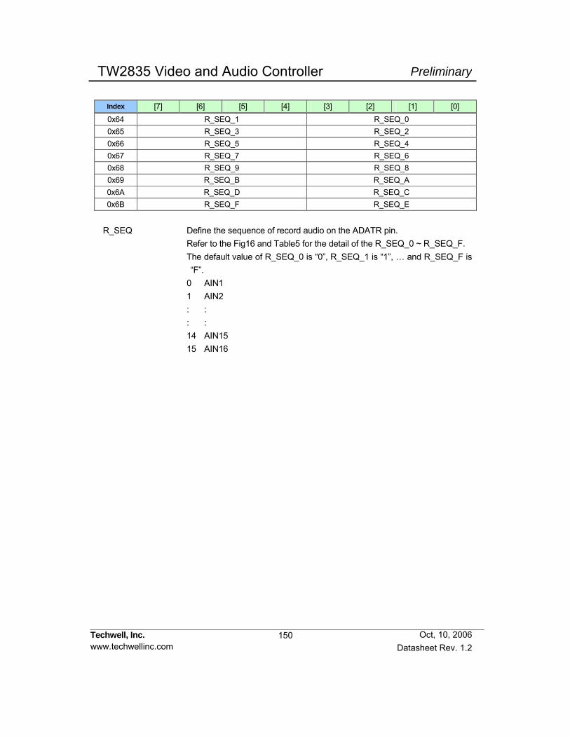
150
PreliminaryTW2835 Video and Audio Controller
Techwell, Inc. www.techwellinc.com Datasheet Rev. 1.2
Oct, 10, 2006
Index [7] [6] [5] [4] [3] [2] [1] [0] 0x64 R_SEQ_1 R_SEQ_0 0x65 R_SEQ_3 R_SEQ_2 0x66 R_SEQ_5 R_SEQ_4 0x67 R_SEQ_7 R_SEQ_6 0x68 R_SEQ_9 R_SEQ_8 0x69 R_SEQ_B R_SEQ_A 0x6A R_SEQ_D R_SEQ_C 0x6B R_SEQ_F R_SEQ_E
R_SEQ Define the sequence of record audio on the ADATR pin. Refer to the Fig16 and Table5 for the detail of the R_SEQ_0 ~ R_SEQ_F. The default value of R_SEQ_0 is “0”, R_SEQ_1 is “1”, … and R_SEQ_F is
“F”. 0 AIN1 1 AIN2 : : : : 14 AIN15 15 AIN16

151
PreliminaryTW2835 Video and Audio Controller
Techwell, Inc. www.techwellinc.com Datasheet Rev. 1.2
Oct, 10, 2006
Index [7] [6] [5] [4] [3] [2] [1] [0]
0x6C 0 PB_
MASTER PB_
LRSEL PB_
BITRATE PB_
DATMODPB_
SAMRATEPB_
BITWID PB_
SYNC
PB_MASTER Define the operation mode of the ACLKP and ASYNP pin for playback. 0 Slaver mode (ACLKP and ASYNP is input mode) (default) 1 Master mode (ACLKP and ASYNP is output mode) PB_LRSEL Select the channel for playback. 0 Left channel audio is used for playback input. (default) 1 Right channel audio is used for playback input. PB_BITRATE Define the bit rate for playback audio on the ACLKP, ASYNP and ADATP
pin. 0 256 bit per sample period (256fs) (default) 1 384 bit per sample period (384fs) PB_DATMOD Define the data mode on the ADATP pin. 0 2’s complement data mode (default) 1 Straight binary data mode PB_SAMRATE Define the sample rate for playback audio on the ACLKP, ASYNP and
ADATP pin. 0 8KHz (default) 1 16KHz PB_BITWID Define the bit width for playback audio on the ADATP pin. 0 16 bit (default) 1 8 bit PB_SYNC Define the digital serial audio data format for playback audio on the ACLKP,
ASYNP and ADATP pin. 0 I2S format (default) 1 DSP format
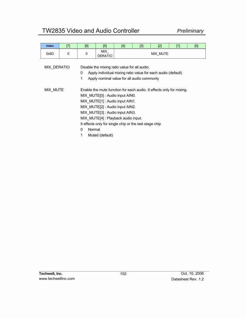
152
PreliminaryTW2835 Video and Audio Controller
Techwell, Inc. www.techwellinc.com Datasheet Rev. 1.2
Oct, 10, 2006
Index [7] [6] [5] [4] [3] [2] [1] [0]
0x6D 0 0 MIX_
DERATIO MIX_MUTE
MIX_DERATIO Disable the mixing ratio value for all audio. 0 Apply individual mixing ratio value for each audio (default) 1 Apply nominal value for all audio commonly MIX_MUTE Enable the mute function for each audio. It effects only for mixing. MIX_MUTE[0] : Audio input AIN0. MIX_MUTE[1] : Audio input AIN1. MIX_MUTE[2] : Audio input AIN2. MIX_MUTE[3] : Audio input AIN3. MIX_MUTE[4] : Playback audio input. It effects only for single chip or the last stage chip 0 Normal 1 Muted (default)
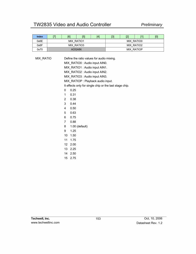
153
PreliminaryTW2835 Video and Audio Controller
Techwell, Inc. www.techwellinc.com Datasheet Rev. 1.2
Oct, 10, 2006
Index [7] [6] [5] [4] [3] [2] [1] [0] 0x6E MIX_RATIO1 MIX_RATIO0 0x6F MIX_RATIO3 MIX_RATIO2 0x70 AOGAIN MIX_RATIOP
MIX_RATIO Define the ratio values for audio mixing. MIX_RATIO0 : Audio input AIN0. MIX_RATIO1 : Audio input AIN1. MIX_RATIO2 : Audio input AIN2. MIX_RATIO3 : Audio input AIN3. MIX_RATIOP : Playback audio input. It effects only for single chip or the last stage chip. 0 0.25 1 0.31 2 0.38 3 0.44 4 0.50 5 0.63 6 0.75 7 0.88 8 1.00 (default) 9 1.25 10 1.50 11 1.75 12 2.00 13 2.25 14 2.50 15 2.75

154
PreliminaryTW2835 Video and Audio Controller
Techwell, Inc. www.techwellinc.com Datasheet Rev. 1.2
Oct, 10, 2006
Index [7] [6] [5] [4] [3] [2] [1] [0] 0x70 AOGAIN MIX_RATIOP
AOGAIN Define the amplifier gain for analog audio output. 0 0.25 1 0.31 2 0.38 3 0.44 4 0.50 5 0.63 6 0.75 7 0.88 8 1.00 (default) 9 1.25 10 1.50 11 1.75 12 2.00 13 2.25 14 2.50 15 2.75

155
PreliminaryTW2835 Video and Audio Controller
Techwell, Inc. www.techwellinc.com Datasheet Rev. 1.2
Oct, 10, 2006
Index [7] [6] [5] [4] [3] [2] [1] [0] 0x71 0 1 MIX_MODE MIX_OUTSEL
MIX_MODE Control the mixing mode for audio mixing. 0 Average mode (default) 1 Just summation mode MIX_OUTSEL Define the final audio output for analog and digital mixing out. 0 Select record audio of channel 0 1 Select record audio of channel 1 2 Select record audio of channel 2 3 Select record audio of channel 3 4 Select record audio of channel 4 5 Select record audio of channel 5 6 Select record audio of channel 6 7 Select record audio of channel 7 8 Select record audio of channel 8 9 Select record audio of channel 9 10 Select record audio of channel 10 11 Select record audio of channel 11 12 Select record audio of channel 12 13 Select record audio of channel 13 14 Select record audio of channel 14 15 Select record audio of channel 15 16 Select playback audio of the first stage chip 17 Select playback audio of the second stage chip 18 Select playback audio of the third stage chip 19 Select playback audio of the last stage chip 20 Select mixed audio (default)
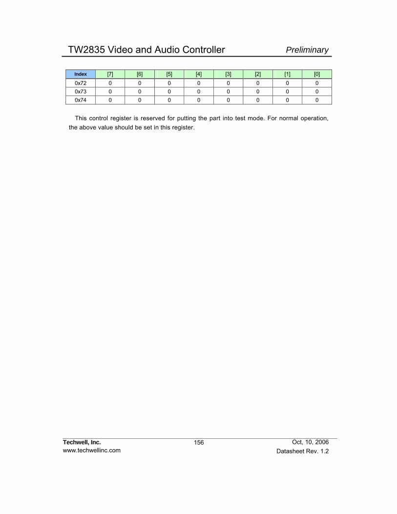
156
PreliminaryTW2835 Video and Audio Controller
Techwell, Inc. www.techwellinc.com Datasheet Rev. 1.2
Oct, 10, 2006
Index [7] [6] [5] [4] [3] [2] [1] [0] 0x72 0 0 0 0 0 0 0 0 0x73 0 0 0 0 0 0 0 0 0x74 0 0 0 0 0 0 0 0
This control register is reserved for putting the part into test mode. For normal operation,
the above value should be set in this register.
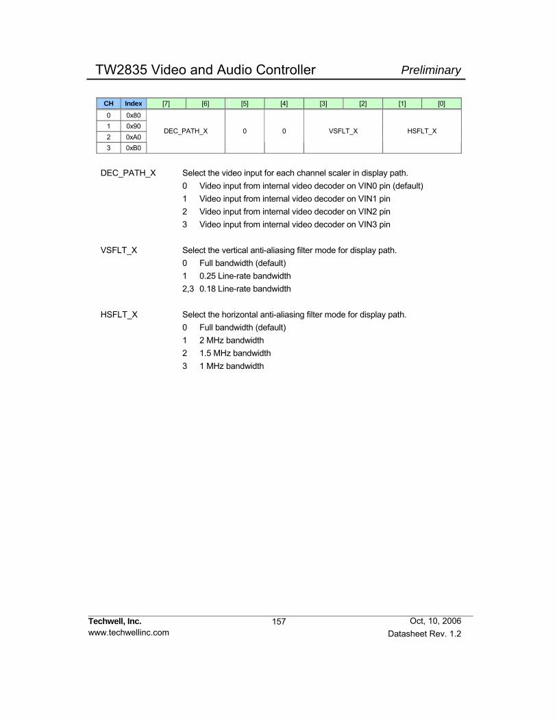
157
PreliminaryTW2835 Video and Audio Controller
Techwell, Inc. www.techwellinc.com Datasheet Rev. 1.2
Oct, 10, 2006
CH Index [7] [6] [5] [4] [3] [2] [1] [0]
0 0x80 1 0x90 2 0xA0 3 0xB0
DEC_PATH_X 0 0 VSFLT_X HSFLT_X
DEC_PATH_X Select the video input for each channel scaler in display path. 0 Video input from internal video decoder on VIN0 pin (default) 1 Video input from internal video decoder on VIN1 pin 2 Video input from internal video decoder on VIN2 pin 3 Video input from internal video decoder on VIN3 pin VSFLT_X Select the vertical anti-aliasing filter mode for display path. 0 Full bandwidth (default) 1 0.25 Line-rate bandwidth 2,3 0.18 Line-rate bandwidth HSFLT_X Select the horizontal anti-aliasing filter mode for display path. 0 Full bandwidth (default) 1 2 MHz bandwidth 2 1.5 MHz bandwidth 3 1 MHz bandwidth

158
PreliminaryTW2835 Video and Audio Controller
Techwell, Inc. www.techwellinc.com Datasheet Rev. 1.2
Oct, 10, 2006
Path CH Index [7] [6] [5] [4] [3] [2] [1] [0]
0 0x81 1 0x91 2 0xA1 3 0xB1
VSCALE_X[15:8]
0 0x82 1 0x92 2 0xA2
X
3 0xB2
VSCALE_X[7:0]
0 0x86 1 0x96 2 0xA6 3 0xB6
VSCALE_PB[15:8]
0 0x87 1 0x97 2 0xA7
PB
3 0xB7
VSCALE_PB[7:0]
VSCALE The 16 bit register defines a vertical scaling ratio. The actual vertical scaling
ratio is VSCALE/(2^16 – 1). The default value is 0xFFFF. Path CH Index [7] [6] [5] [4] [3] [2] [1] [0]
0 0x83 1 0x93 2 0xA3 3 0xB3
HSCALE_X[15:8]
0 0x84 1 0x94 2 0xA4
X
3 0xB4
HSCALE_X[7:0]
0 0x88 1 0x98 2 0xA8 3 0xB8
HSCALE_PB[15:8]
0 0x89 1 0x99 2 0xA9
PB
3 0xB9
HSCALE_PB[7:0]
HSCALE The 16 bit register defines a horizontal scaling ratio. The actual horizontal
scaling ratio is HSCALE/(2^16 – 1). The default value is 0xFFFF.

159
PreliminaryTW2835 Video and Audio Controller
Techwell, Inc. www.techwellinc.com Datasheet Rev. 1.2
Oct, 10, 2006
CH Index [7] [6] [5] [4] [3] [2] [1] [0]
0 0x85 1 0x95 2 0xA5 3 0xB5
0 0 0 0 VSFLT_PB HSFLT_PB
VSFLT_PB Select the vertical anti-aliasing filter mode for PB path. 0 Full bandwidth (default) 1 0.25 Line-rate bandwidth 2,3 0.18 Line-rate bandwidth HSFLT_PB Select the horizontal anti-aliasing filter mode for PB path. 0 Full bandwidth (default) 1 2 MHz bandwidth 2 1.5 MHz bandwidth 3 1 MHz bandwidth
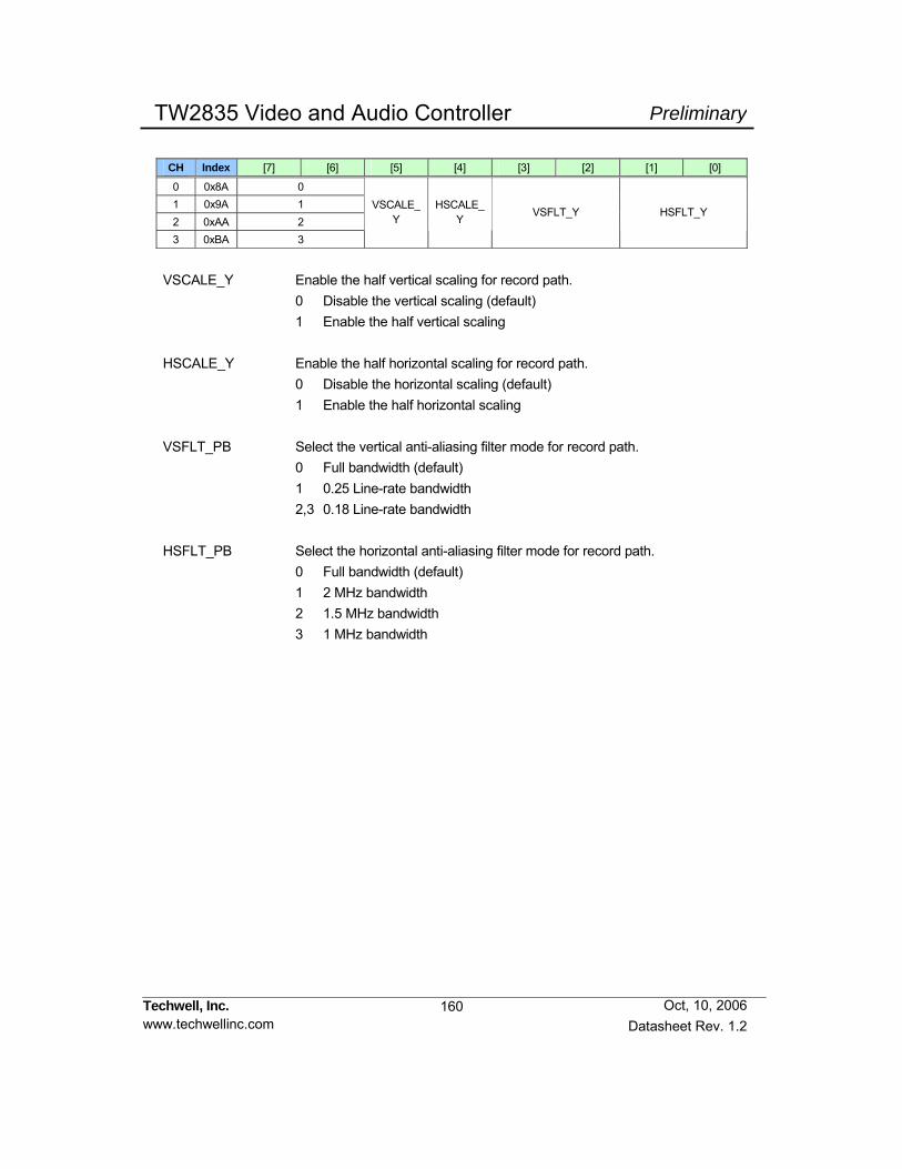
160
PreliminaryTW2835 Video and Audio Controller
Techwell, Inc. www.techwellinc.com Datasheet Rev. 1.2
Oct, 10, 2006
CH Index [7] [6] [5] [4] [3] [2] [1] [0]
0 0x8A 0 1 0x9A 1 2 0xAA 2 3 0xBA 3
VSCALE_ Y
HSCALE_ Y VSFLT_Y HSFLT_Y
VSCALE_Y Enable the half vertical scaling for record path. 0 Disable the vertical scaling (default) 1 Enable the half vertical scaling HSCALE_Y Enable the half horizontal scaling for record path. 0 Disable the horizontal scaling (default) 1 Enable the half horizontal scaling VSFLT_PB Select the vertical anti-aliasing filter mode for record path. 0 Full bandwidth (default) 1 0.25 Line-rate bandwidth 2,3 0.18 Line-rate bandwidth HSFLT_PB Select the horizontal anti-aliasing filter mode for record path. 0 Full bandwidth (default) 1 2 MHz bandwidth 2 1.5 MHz bandwidth 3 1 MHz bandwidth
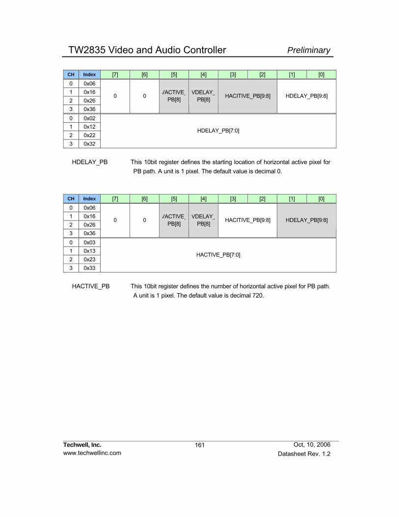
161
PreliminaryTW2835 Video and Audio Controller
Techwell, Inc. www.techwellinc.com Datasheet Rev. 1.2
Oct, 10, 2006
CH Index [7] [6] [5] [4] [3] [2] [1] [0] 0 0x06 1 0x16 2 0x26 3 0x36
0 0 VACTIVE_PB[8]
VDELAY_PB[8] HACITIVE_PB[9:8] HDELAY_PB[9:8]
0 0x02 1 0x12 2 0x22 3 0x32
HDELAY_PB[7:0]
HDELAY_PB This 10bit register defines the starting location of horizontal active pixel for
PB path. A unit is 1 pixel. The default value is decimal 0.
CH Index [7] [6] [5] [4] [3] [2] [1] [0] 0 0x06 1 0x16 2 0x26 3 0x36
0 0 VACTIVE_PB[8]
VDELAY_PB[8]
HACITIVE_PB[9:8] HDELAY_PB[9:8]
0 0x03 1 0x13 2 0x23 3 0x33
HACTIVE_PB[7:0]
HACTIVE_PB This 10bit register defines the number of horizontal active pixel for PB path.
A unit is 1 pixel. The default value is decimal 720.
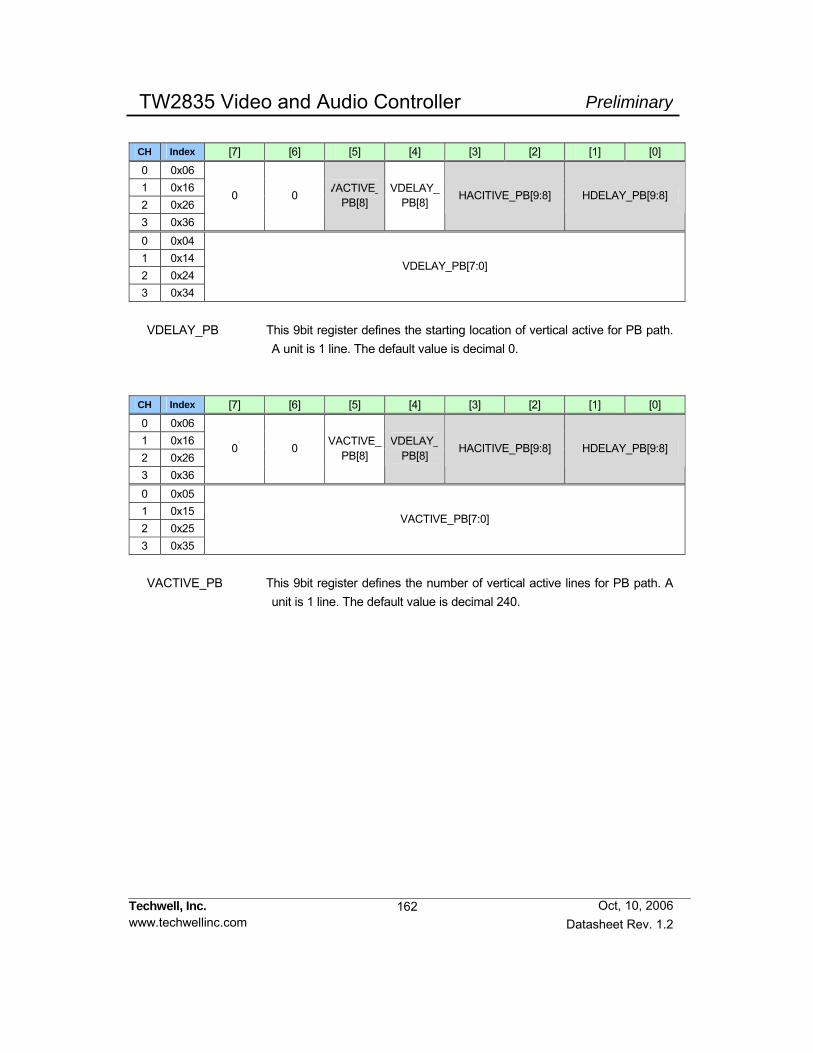
162
PreliminaryTW2835 Video and Audio Controller
Techwell, Inc. www.techwellinc.com Datasheet Rev. 1.2
Oct, 10, 2006
CH Index [7] [6] [5] [4] [3] [2] [1] [0] 0 0x06 1 0x16 2 0x26 3 0x36
0 0 VACTIVE_PB[8]
VDELAY_PB[8] HACITIVE_PB[9:8] HDELAY_PB[9:8]
0 0x04 1 0x14 2 0x24 3 0x34
VDELAY_PB[7:0]
VDELAY_PB This 9bit register defines the starting location of vertical active for PB path.
A unit is 1 line. The default value is decimal 0.
CH Index [7] [6] [5] [4] [3] [2] [1] [0] 0 0x06 1 0x16 2 0x26 3 0x36
0 0 VACTIVE_PB[8]
VDELAY_PB[8]
HACITIVE_PB[9:8] HDELAY_PB[9:8]
0 0x05 1 0x15 2 0x25 3 0x35
VACTIVE_PB[7:0]
VACTIVE_PB This 9bit register defines the number of vertical active lines for PB path. A
unit is 1 line. The default value is decimal 240.
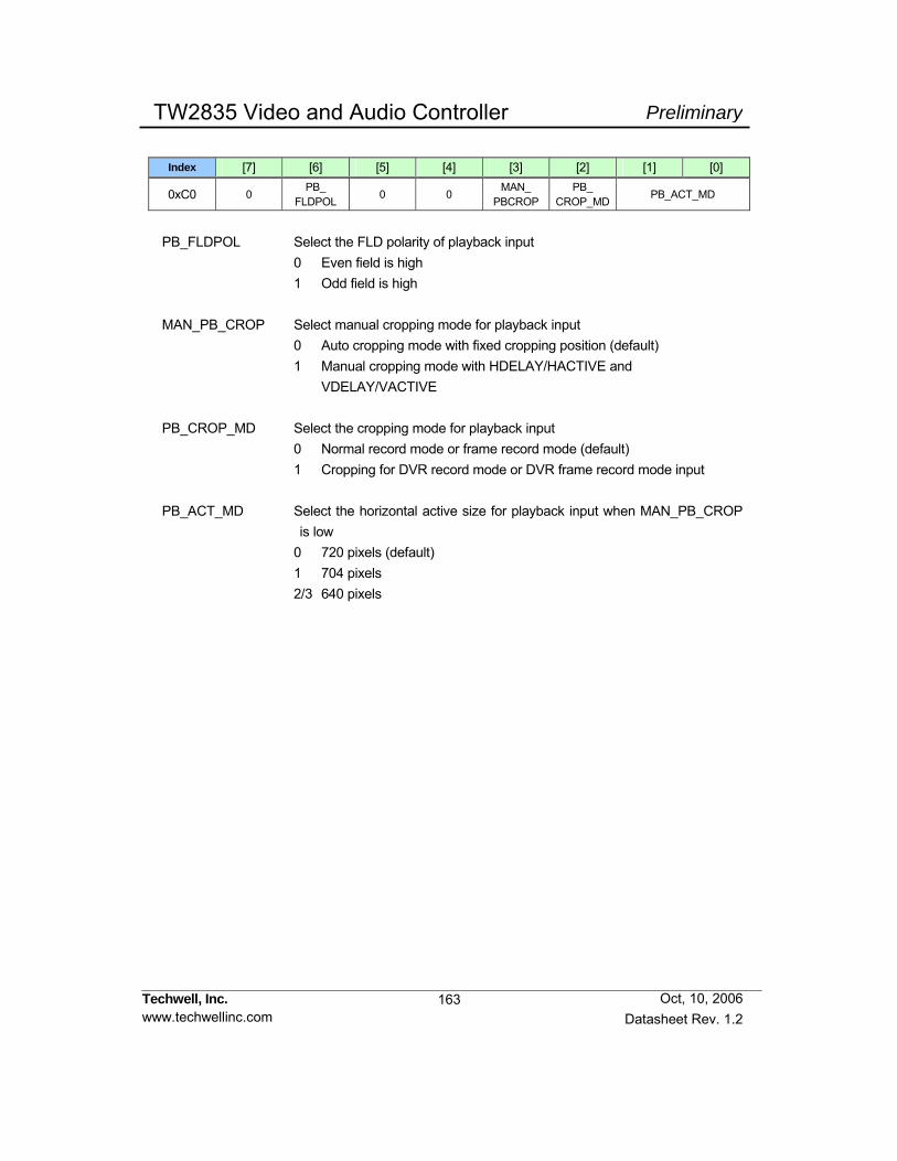
163
PreliminaryTW2835 Video and Audio Controller
Techwell, Inc. www.techwellinc.com Datasheet Rev. 1.2
Oct, 10, 2006
Index [7] [6] [5] [4] [3] [2] [1] [0]
0xC0 0 PB_
FLDPOL 0 0
MAN_ PBCROP
PB_ CROP_MD
PB_ACT_MD
PB_FLDPOL Select the FLD polarity of playback input 0 Even field is high 1 Odd field is high MAN_PB_CROP Select manual cropping mode for playback input 0 Auto cropping mode with fixed cropping position (default) 1 Manual cropping mode with HDELAY/HACTIVE and VDELAY/VACTIVE
PB_CROP_MD Select the cropping mode for playback input 0 Normal record mode or frame record mode (default) 1 Cropping for DVR record mode or DVR frame record mode input
PB_ACT_MD Select the horizontal active size for playback input when MAN_PB_CROP is low
0 720 pixels (default) 1 704 pixels 2/3 640 pixels
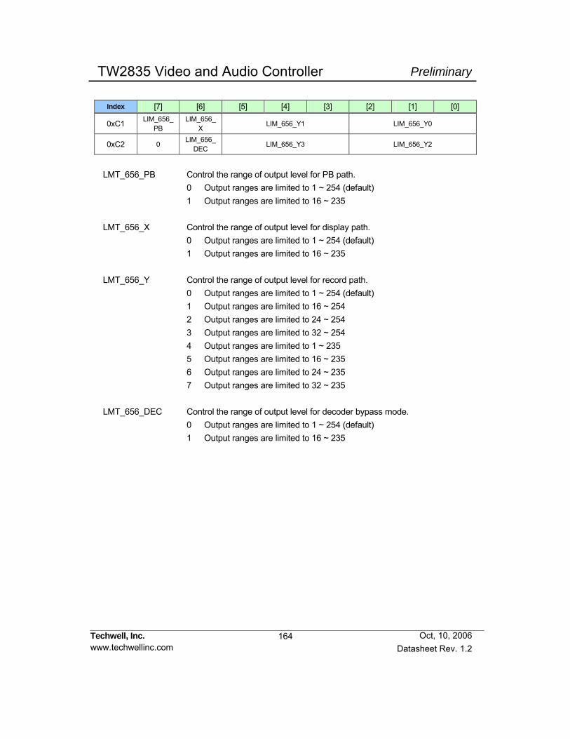
164
PreliminaryTW2835 Video and Audio Controller
Techwell, Inc. www.techwellinc.com Datasheet Rev. 1.2
Oct, 10, 2006
Index [7] [6] [5] [4] [3] [2] [1] [0]
0xC1 LIM_656_ PB
LIM_656_ X
LIM_656_Y1 LIM_656_Y0
0xC2 0 LIM_656_
DEC LIM_656_Y3 LIM_656_Y2
LMT_656_PB Control the range of output level for PB path. 0 Output ranges are limited to 1 ~ 254 (default) 1 Output ranges are limited to 16 ~ 235 LMT_656_X Control the range of output level for display path. 0 Output ranges are limited to 1 ~ 254 (default) 1 Output ranges are limited to 16 ~ 235 LMT_656_Y Control the range of output level for record path. 0 Output ranges are limited to 1 ~ 254 (default) 1 Output ranges are limited to 16 ~ 254 2 Output ranges are limited to 24 ~ 254 3 Output ranges are limited to 32 ~ 254 4 Output ranges are limited to 1 ~ 235 5 Output ranges are limited to 16 ~ 235 6 Output ranges are limited to 24 ~ 235 7 Output ranges are limited to 32 ~ 235 LMT_656_DEC Control the range of output level for decoder bypass mode. 0 Output ranges are limited to 1 ~ 254 (default) 1 Output ranges are limited to 16 ~ 235

165
PreliminaryTW2835 Video and Audio Controller
Techwell, Inc. www.techwellinc.com Datasheet Rev. 1.2
Oct, 10, 2006
Index [7] [6] [5] [4] [3] [2] [1] [0]
0xC3 BGNDEN_PB BGNDCOL AUTO
BGNDPB AUTO
BGNDY AUTO
BGNDX
0xC4 BGNDEN_Y BGNDEN_X
BGNDEN Enable the background color for each channel. BGNDEN[3:0] stands for CH3 to CH0. 0 Background color is disabled (default) 1 Background color is enabled
BLKCOL Select the background color when BGNDEN = “1”. 0 Blue color (default) 1 Black color AUTO_BGND Select the decoder background mode. 0 Manual background mode (default) 1 Automatic background mode when No-video is detected.
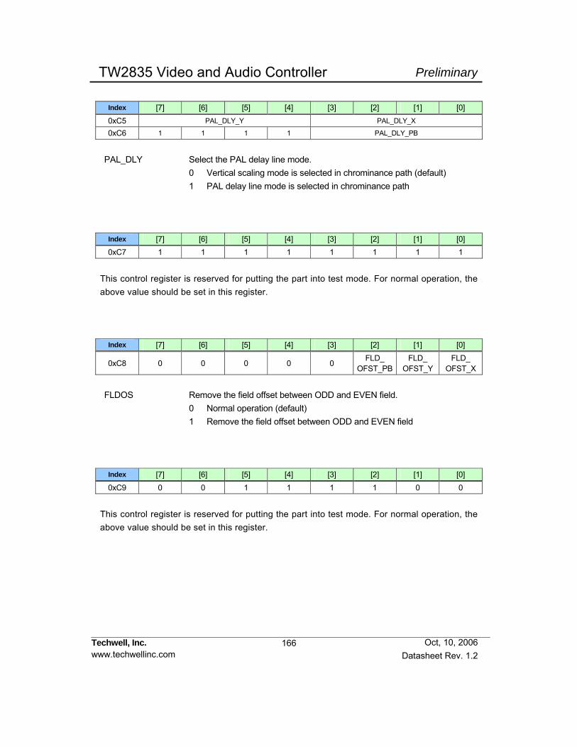
166
PreliminaryTW2835 Video and Audio Controller
Techwell, Inc. www.techwellinc.com Datasheet Rev. 1.2
Oct, 10, 2006
Index [7] [6] [5] [4] [3] [2] [1] [0] 0xC5 PAL_DLY_Y PAL_DLY_X
0xC6 1 1 1 1 PAL_DLY_PB
PAL_DLY Select the PAL delay line mode. 0 Vertical scaling mode is selected in chrominance path (default) 1 PAL delay line mode is selected in chrominance path
Index [7] [6] [5] [4] [3] [2] [1] [0] 0xC7 1 1 1 1 1 1 1 1
This control register is reserved for putting the part into test mode. For normal operation, the above value should be set in this register.
Index [7] [6] [5] [4] [3] [2] [1] [0]
0xC8 0 0 0 0 0 FLD_ OFST_PB
FLD_ OFST_Y
FLD_ OFST_X
FLDOS Remove the field offset between ODD and EVEN field. 0 Normal operation (default) 1 Remove the field offset between ODD and EVEN field
Index [7] [6] [5] [4] [3] [2] [1] [0] 0xC9 0 0 1 1 1 1 0 0
This control register is reserved for putting the part into test mode. For normal operation, the above value should be set in this register.
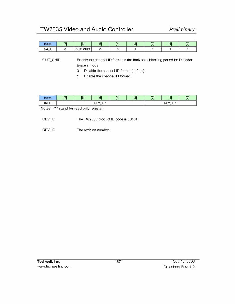
167
PreliminaryTW2835 Video and Audio Controller
Techwell, Inc. www.techwellinc.com Datasheet Rev. 1.2
Oct, 10, 2006
Index [7] [6] [5] [4] [3] [2] [1] [0] 0xCA 0 OUT_CHID 0 0 1 1 1 1
OUT_CHID Enable the channel ID format in the horizontal blanking period for Decoder Bypass mode 0 Disable the channel ID format (default) 1 Enable the channel ID format
Index [7] [6] [5] [4] [3] [2] [1] [0] 0xFE DEV_ID * REV_ID *
Notes “*” stand for read only register DEV_ID The TW2835 product ID code is 00101. REV_ID The revision number.

168
PreliminaryTW2835 Video and Audio Controller
Techwell, Inc. www.techwellinc.com Datasheet Rev. 1.2
Oct, 10, 2006
Index [7] [6] [5] [4] [3] [2] [1] [0]
1x00 SYS_5060 OVERLAY LINK _LAST_X
LINK _LAST_Y LINK_EN_X LINK_EN_Y LINK_NUM
SYS_5060 Select the standard format for video controller. 0 60Hz, 525 line format (default) 1 50Hz, 625 line format OVERLAY Control the overlay between display and record path. 0 Disable the overlay (default) 1 Enable the overlay LINK_LAST Define the lowest slaver chip in chip-to-chip cascade operation. 0 Master or middle slaver chip (default) 1 The lowest slaver chip LINK_EN Control the chip-to-chip cascade operation for display and record path. 0 Disable the cascade operation (default) 1 Enable the cascade operation LINK_NUM Define the stage number of chip-to-chip cascade connection. 0 Master chip (default) 1 1st slaver chip 2 2nd slaver chip 3 3rd slaver chip
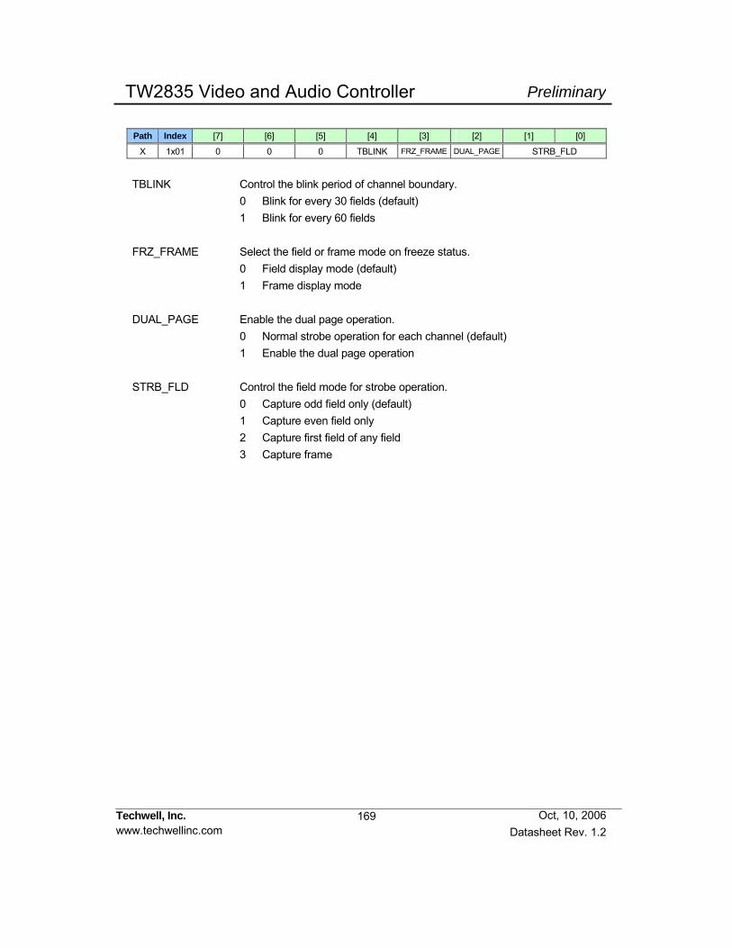
169
PreliminaryTW2835 Video and Audio Controller
Techwell, Inc. www.techwellinc.com Datasheet Rev. 1.2
Oct, 10, 2006
Path Index [7] [6] [5] [4] [3] [2] [1] [0]
X 1x01 0 0 0 TBLINK FRZ_FRAME DUAL_PAGE STRB_FLD
TBLINK Control the blink period of channel boundary. 0 Blink for every 30 fields (default) 1 Blink for every 60 fields FRZ_FRAME Select the field or frame mode on freeze status. 0 Field display mode (default) 1 Frame display mode DUAL_PAGE Enable the dual page operation. 0 Normal strobe operation for each channel (default) 1 Enable the dual page operation STRB_FLD Control the field mode for strobe operation. 0 Capture odd field only (default) 1 Capture even field only 2 Capture first field of any field 3 Capture frame
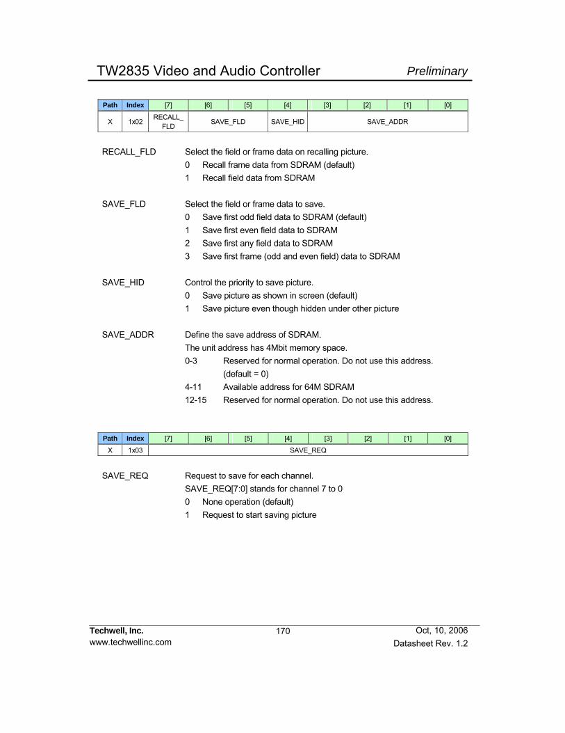
170
PreliminaryTW2835 Video and Audio Controller
Techwell, Inc. www.techwellinc.com Datasheet Rev. 1.2
Oct, 10, 2006
Path Index [7] [6] [5] [4] [3] [2] [1] [0]
X 1x02 RECALL_ FLD
SAVE_FLD SAVE_HID SAVE_ADDR
RECALL_FLD Select the field or frame data on recalling picture. 0 Recall frame data from SDRAM (default) 1 Recall field data from SDRAM SAVE_FLD Select the field or frame data to save. 0 Save first odd field data to SDRAM (default) 1 Save first even field data to SDRAM 2 Save first any field data to SDRAM 3 Save first frame (odd and even field) data to SDRAM SAVE_HID Control the priority to save picture. 0 Save picture as shown in screen (default) 1 Save picture even though hidden under other picture SAVE_ADDR Define the save address of SDRAM. The unit address has 4Mbit memory space. 0-3 Reserved for normal operation. Do not use this address. (default = 0) 4-11 Available address for 64M SDRAM 12-15 Reserved for normal operation. Do not use this address.
Path Index [7] [6] [5] [4] [3] [2] [1] [0]
X 1x03 SAVE_REQ
SAVE_REQ Request to save for each channel. SAVE_REQ[7:0] stands for channel 7 to 0 0 None operation (default) 1 Request to start saving picture

171
PreliminaryTW2835 Video and Audio Controller
Techwell, Inc. www.techwellinc.com Datasheet Rev. 1.2
Oct, 10, 2006
Path Index [7] [6] [5] [4] [3] [2] [1] [0]
X 1x04 STRB_REQ
STRB_REQ Request strobe operation. STRB_REQ[7:0] stands for channel 7 to 0 0 None operation (default) 1 Request to start strobe operation Path Index [7] [6] [5] [4] [3] [2] [1] [0]
X 1x05 NOVID_MODE 0 0 0 AUTO_ ENHANCE
INVALID_MODE
NOVID_MODE Select the indication method for no-video channel 0 Bypass (default) 1 Capture last image 2 Blanked with blank color 3 Capture last image and blink channel boundary AUTO_ENHANCE Enable auto enhancement mode in field display mode 0 Manual enhancement mode in field display mode (default) 1 Auto enhancement mode in field display mode INVALID_MODE Select the indication mode for no channel area In horizontal and vertical active region 0 Background layer with background color (default) 1 Y = 0, Cb/Cr = 128 2 Y/Cb/Cr = 0 3 Y/Cb/Cr = 0
In horizontal and vertical blanking region 0 Y = 16, Cb/Cr = 128 (default) 1 Background layer with background color 2 Y = 0, Cb = 0, F, V, 0, Cascade, linenum[8:7], Cr = 0, linenum[6:0] 3 Y/Cb/Cr = 0
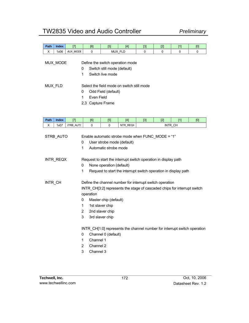
172
PreliminaryTW2835 Video and Audio Controller
Techwell, Inc. www.techwellinc.com Datasheet Rev. 1.2
Oct, 10, 2006
Path Index [7] [6] [5] [4] [3] [2] [1] [0]
X 1x06 MUX_MODE 0 MUX_FLD 0 0 0 0
MUX_MODE Define the switch operation mode 0 Switch still mode (default) 1 Switch live mode MUX_FLD Select the field mode on switch still mode 0 Odd Field (default) 1 Even Field 2,3 Capture Frame Path Index [7] [6] [5] [4] [3] [2] [1] [0]
X 1x07 STRB_AUTO 0 0 INTR_REQX INTR_CH
STRB_AUTO Enable automatic strobe mode when FUNC_MODE = “1” 0 User strobe mode (default) 1 Automatic strobe mode INTR_REQX Request to start the interrupt switch operation in display path 0 None operation (default) 1 Request to start the interrupt switch operation in display path INTR_CH Define the channel number for interrupt switch operation INTR_CH[3:2] represents the stage of cascaded chips for interrupt switch operation 0 Master chip (default) 1 1st slaver chip 2 2nd slaver chip 3 3rd slaver chip INTR_CH[1:0] represents the channel number for interrupt switch operation 0 Channel 0 (default) 1 Channel 1 2 Channel 2 3 Channel 3
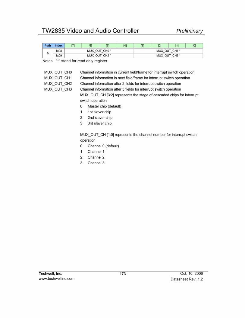
173
PreliminaryTW2835 Video and Audio Controller
Techwell, Inc. www.techwellinc.com Datasheet Rev. 1.2
Oct, 10, 2006
Path Index [7] [6] [5] [4] [3] [2] [1] [0]
1x08 MUX_OUT_CH0 * MUX_OUT_CH1 * X
1x09 MUX_OUT_CH2 * MUX_OUT_CH3 *
Notes “*” stand for read only register
MUX_OUT_CH0 Channel information in current field/frame for interrupt switch operation MUX_OUT_CH1 Channel information in next field/frame for interrupt switch operation MUX_OUT_CH2 Channel information after 2 fields for interrupt switch operation MUX_OUT_CH3 Channel information after 3 fields for interrupt switch operation MUX_OUT_CH [3:2] represents the stage of cascaded chips for interrupt switch operation 0 Master chip (default) 1 1st slaver chip 2 2nd slaver chip 3 3rd slaver chip MUX_OUT_CH [1:0] represents the channel number for interrupt switch operation 0 Channel 0 (default) 1 Channel 1 2 Channel 2 3 Channel 3

174
PreliminaryTW2835 Video and Audio Controller
Techwell, Inc. www.techwellinc.com Datasheet Rev. 1.2
Oct, 10, 2006
Path Index [7] [6] [5] [4] [3] [2] [1] [0]
X 1x0A CHID_MUX_OUT *
Notes “*” stand for read only register CHID_MUX_OUT Channel ID of current field/frame in interrupt switch operation CHID_MUX_OUT [7] represents the channel ID latch enabling pulse 0->1 Rising edge for channel ID Update 1->0 Falling edge after 16 clock * 18.5 ns from rising edge CHID_MUX_OUT [6] represents the updated picture in interrupt switch operation 0 No Updated 1 Updated by new switching CHID_MUX_OUT [5] represents the field mode in interrupt switch operation 0 Frame Mode 1 Field Mode CHID_MUX_OUT [4] represents the analog switch path 0 Analog switch 0 path 1 Analog switch 1 path CHID_MUX_OUT [3:2] represents the stage of cascaded chips for interrupt switch operation 0 Master chip 1 1st slaver chip 2 2nd slaver chip 3 3rd slaver chip CHID_MUX_OUT [1:0] represents the channel number for interrupt switch operation 0 Channel 0 1 Channel 1 2 Channel 2 3 Channel 3
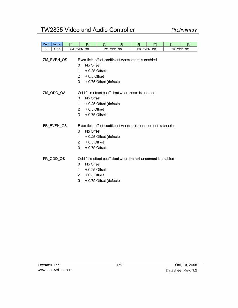
175
PreliminaryTW2835 Video and Audio Controller
Techwell, Inc. www.techwellinc.com Datasheet Rev. 1.2
Oct, 10, 2006
Path Index [7] [6] [5] [4] [3] [2] [1] [0]
X 1x0B ZM_EVEN_OS ZM_ODD_OS FR_EVEN_OS FR_ODD_OS
ZM_EVEN_OS Even field offset coefficient when zoom is enabled 0 No Offset 1 + 0.25 Offset 2 + 0.5 Offset 3 + 0.75 Offset (default)
ZM_ODD_OS Odd field offset coefficient when zoom is enabled 0 No Offset 1 + 0.25 Offset (default) 2 + 0.5 Offset 3 + 0.75 Offset
FR_EVEN_OS Even field offset coefficient when the enhancement is enabled 0 No Offset 1 + 0.25 Offset (default) 2 + 0.5 Offset 3 + 0.75 Offset
FR_ODD_OS Odd field offset coefficient when the enhancement is enabled 0 No Offset 1 + 0.25 Offset 2 + 0.5 Offset 3 + 0.75 Offset (default)

176
PreliminaryTW2835 Video and Audio Controller
Techwell, Inc. www.techwellinc.com Datasheet Rev. 1.2
Oct, 10, 2006
Path Index [7] [6] [5] [4] [3] [2] [1] [0]
X 1x0C ZMENA H_ZM_MD ZMBNDCOL ZMBNDEN ZMAREAEN ZMAREA
ZMENA Enable the zoom function. 0 Disable the zoom function (default) 1 Enable the zoom function H_ZM_MD Select the zoom mode for only horizontal direction 0 2x zoom for both horizontal and vertical direction (default) 1 2x zoom for horizontal direction ZMBNDCOL Define the boundary color for zoomed area 0 0% Black (default) 1 25% Gray 2 75% Gray 3 100% White ZMBNDEN Enable the boundary for zoomed area. 0 Disable the boundary for zoomed area (default) 1 Enable the boundary for zoomed area ZMAREAEN Enable the mark for zoomed area 0 Disable the mark for zoom area (default) 1 Enable the mark for zoom area ZMAREA Control the effect for zoomed area. 0 10 IRE bright up for inside of zoomed area (default) 1 20 IRE bright up for inside of zoomed area 2 10 IRE bright up for outside of zoomed area 3 20 IRE bright up for outside of zoomed area

177
PreliminaryTW2835 Video and Audio Controller
Techwell, Inc. www.techwellinc.com Datasheet Rev. 1.2
Oct, 10, 2006
Path Index [7] [6] [5] [4] [3] [2] [1] [0]
X 1x0D ZOOMH
ZOOMH Define the horizontal left point of zoomed area. 4 pixels/step. 0 Left end value (default) : : 180 Right end value
Path Index [7] [6] [5] [4] [3] [2] [1] [0]
X 1x0E ZOOMV
ZOOMV Define the vertical top point of zoom area. 2 lines/step. 0 Top end value (default) : : 120 Bottom end value for 60Hz, 525 lines system : : 144 Bottom end value for 50Hz, 625 lines system

178
PreliminaryTW2835 Video and Audio Controller
Techwell, Inc. www.techwellinc.com Datasheet Rev. 1.2
Oct, 10, 2006
Path Index [7] [6] [5] [4] [3] [2] [1] [0]
X 1x0F FRZ_FLD BNDCOL BGDCOL BLKCOL
FRZ_FLD Select the image for freeze function or for last image capture on video loss. 0 Last image (default) 1 Last image of 1 field before 2 Last image of 2 fields before 3 Last image of 3 fields before BNDCOL Define the channel boundary color. 0 0% Black 1 25% Gray 2 75% Gray 3 100% White (default) Channel boundary color is changed according to this value when boundary
is blinking. 0 100% White 1 100% White 2 0% Black 3 0% Black (default) BGDCOL Define the background color. 0 0% Black 1 40% Gray (default) 2 75% Gray 3 100% Amplitude 100% Saturation Blue BLKCOL Define the color of the blanked channel. 0 0% Black 1 40% Gray 2 75% Gray 3 100% Amplitude 100% Saturation Blue (default)
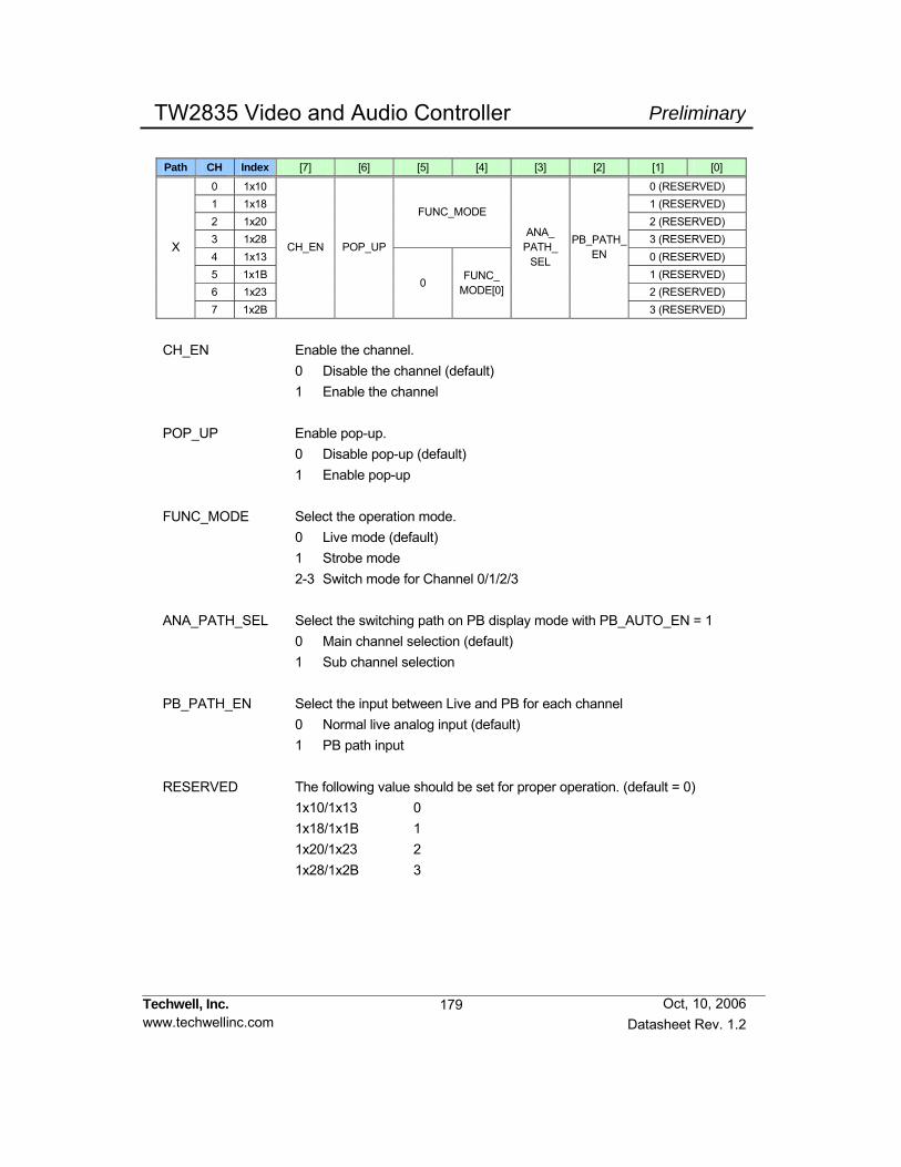
179
PreliminaryTW2835 Video and Audio Controller
Techwell, Inc. www.techwellinc.com Datasheet Rev. 1.2
Oct, 10, 2006
Path CH Index [7] [6] [5] [4] [3] [2] [1] [0]
0 1x10 0 (RESERVED) 1 1x18 1 (RESERVED) 2 1x20 2 (RESERVED) 3 1x28
FUNC_MODE
3 (RESERVED) 4 1x13 0 (RESERVED) 5 1x1B 1 (RESERVED) 6 1x23 2 (RESERVED)
X
7 1x2B
CH_EN POP_UP
0 FUNC_
MODE[0]
ANA_ PATH_
SEL
PB_PATH_EN
3 (RESERVED)
CH_EN Enable the channel. 0 Disable the channel (default) 1 Enable the channel POP_UP Enable pop-up. 0 Disable pop-up (default) 1 Enable pop-up FUNC_MODE Select the operation mode. 0 Live mode (default) 1 Strobe mode 2-3 Switch mode for Channel 0/1/2/3 ANA_PATH_SEL Select the switching path on PB display mode with PB_AUTO_EN = 1 0 Main channel selection (default) 1 Sub channel selection PB_PATH_EN Select the input between Live and PB for each channel 0 Normal live analog input (default) 1 PB path input RESERVED The following value should be set for proper operation. (default = 0) 1x10/1x13 0 1x18/1x1B 1 1x20/1x23 2 1x28/1x2B 3

180
PreliminaryTW2835 Video and Audio Controller
Techwell, Inc. www.techwellinc.com Datasheet Rev. 1.2
Oct, 10, 2006
Path CH Index [7] [6] [5] [4] [3] [2] [1] [0]
0 1x11 1 1x19 2 1x21 3 1x29 4 1x14 5 1x1C 6 1x24
X
7 1x2C
RECALL_ EN FREEZE H_MIRRORV_MIRROR ENHANCE BLANK BOUND BLINK
RECALL_EN Enable the recall function of main channel. 0 Disable the recall function (default) 1 Enable the recall function FREEZE Enable the freeze function of main channel. 0 Normal operation (default) 1 Enable the freeze function H_MIRROR Enable the horizontal mirroring function of main channel. 0 Normal operation (default) 1 Enable the horizontal mirroring function V_MIRROR Enable the vertical mirroring function of main channel. 0 Normal operation (default) 1 Enable the vertical mirroring function ENHANCE Enable the image enhancement function of main channel. 0 Normal operation (default) 1 Enable the image enhancement function BLANK Enable the blank of main channel. 0 Disable the blank (default) 1 Enable the blank BOUND Enable the channel boundary of main channel. 0 Disable the channel boundary (default) 1 Enable the channel boundary BLINK Enable the boundary blink of main channel when boundary is enabled. 0 Disable the boundary blink (default) 1 Enable the boundary blink

181
PreliminaryTW2835 Video and Audio Controller
Techwell, Inc. www.techwellinc.com Datasheet Rev. 1.2
Oct, 10, 2006
Path CH Index [7] [6] [5] [4] [3] [2] [1] [0]
0 1x12 1 1x1A 2 1x22 3 1x2A 4 1x15 5 1x1D 6 1x25
X
7 1x2D
0 0 FLD_OP DVR_IN RECALL_ADDR
FLD_OP Enable Field to Frame conversion mode. 0 Normal operation (default) 1 Enable Field to Frame conversion mode DVR_IN Enable DVR to normal conversion mode. 0 Normal operation (default) 1 DVR to normal conversion mode RECALL_ADDR Define the recall address for main channel. (default = 0) 0-3 Reserved address. Do not use this value 4-15 Available address for 64M SDRAM
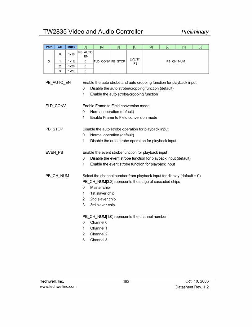
182
PreliminaryTW2835 Video and Audio Controller
Techwell, Inc. www.techwellinc.com Datasheet Rev. 1.2
Oct, 10, 2006
Path CH Index [7] [6] [5] [4] [3] [2] [1] [0]
0 1x16 PB_AUTO _EN
1 1x1E 0 2 1x26 0
X
3 1x2E 0
FLD_CONV PB_STOP EVENT _PB
PB_CH_NUM
PB_AUTO_EN Enable the auto strobe and auto cropping function for playback input 0 Disable the auto strobe/cropping function (default) 1 Enable the auto strobe/cropping function FLD_CONV Enable Frame to Field conversion mode 0 Normal operation (default) 1 Enable Frame to Field conversion mode PB_STOP Disable the auto strobe operation for playback input 0 Normal operation (default) 1 Disable the auto strobe operation for playback input EVEN_PB Enable the event strobe function for playback input 0 Disable the event strobe function for playback input (default) 1 Enable the event strobe function for playback input PB_CH_NUM Select the channel number from playback input for display (default = 0) PB_CH_NUM[3:2] represents the stage of cascaded chips 0 Master chip 1 1st slaver chip 2 2nd slaver chip 3 3rd slaver chip PB_CH_NUM[1:0] represents the channel number 0 Channel 0 1 Channel 1 2 Channel 2 3 Channel 3
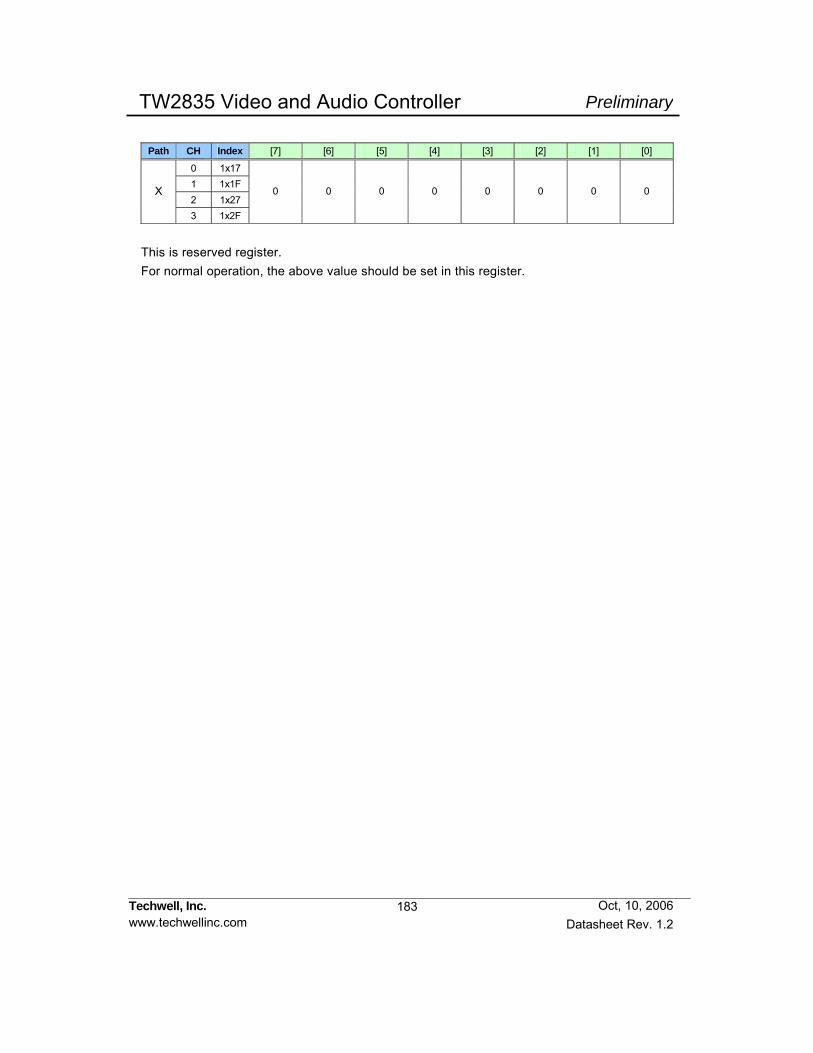
183
PreliminaryTW2835 Video and Audio Controller
Techwell, Inc. www.techwellinc.com Datasheet Rev. 1.2
Oct, 10, 2006
Path CH Index [7] [6] [5] [4] [3] [2] [1] [0]
0 1x17 1 1x1F 2 1x27
X
3 1x2F
0 0 0 0 0 0 0 0
This is reserved register. For normal operation, the above value should be set in this register.

184
PreliminaryTW2835 Video and Audio Controller
Techwell, Inc. www.techwellinc.com Datasheet Rev. 1.2
Oct, 10, 2006
Path CH Index [7] [6] [5] [4] [3] [2] [1] [0]
0 1x30 1 1x34 2 1x38 3 1x3C 4 1x40 5 1x44 6 1x48
X
7 1x4C
PICHL
PICHL Define the horizontal left position of channel 0 Left end (default) : : 180 Right end Path CH Index [7] [6] [5] [4] [3] [2] [1] [0]
0 1x31 1 1x35 2 1x39 3 1x3D 4 1x41 5 1x45 6 1x49
X
7 1x4D
PICHR
PICHR Define the horizontal right position of channel region 0 Left end (default) : : 180 Right end
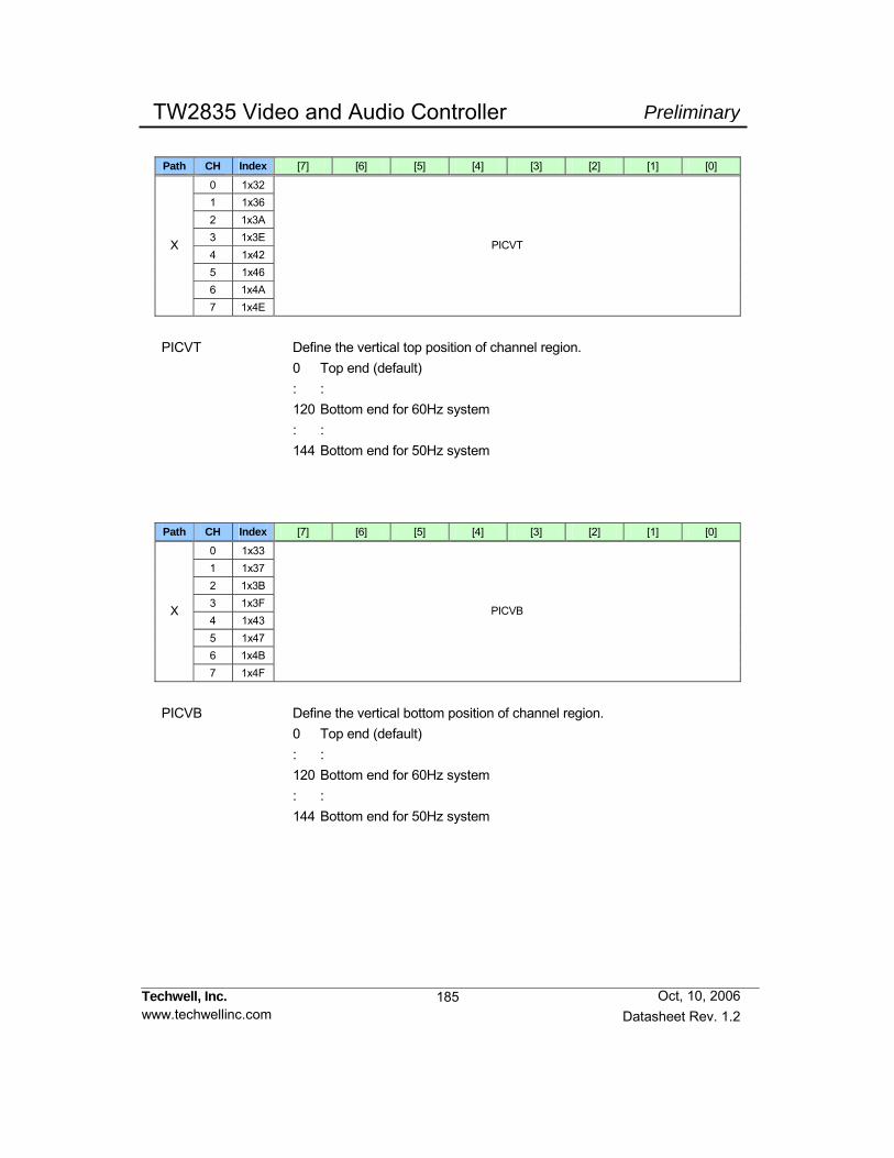
185
PreliminaryTW2835 Video and Audio Controller
Techwell, Inc. www.techwellinc.com Datasheet Rev. 1.2
Oct, 10, 2006
Path CH Index [7] [6] [5] [4] [3] [2] [1] [0]
0 1x32 1 1x36 2 1x3A 3 1x3E 4 1x42 5 1x46 6 1x4A
X
7 1x4E
PICVT
PICVT Define the vertical top position of channel region. 0 Top end (default) : : 120 Bottom end for 60Hz system : : 144 Bottom end for 50Hz system Path CH Index [7] [6] [5] [4] [3] [2] [1] [0]
0 1x33 1 1x37 2 1x3B 3 1x3F 4 1x43 5 1x47 6 1x4B
X
7 1x4F
PICVB
PICVB Define the vertical bottom position of channel region. 0 Top end (default) : : 120 Bottom end for 60Hz system : : 144 Bottom end for 50Hz system
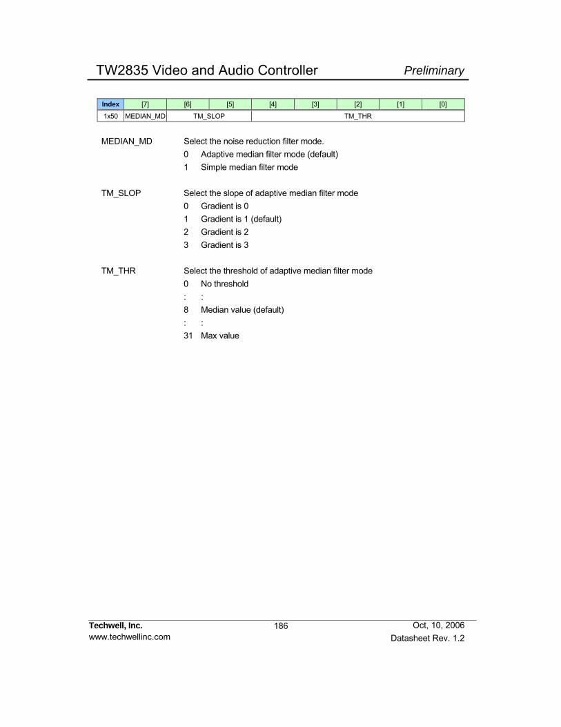
186
PreliminaryTW2835 Video and Audio Controller
Techwell, Inc. www.techwellinc.com Datasheet Rev. 1.2
Oct, 10, 2006
Index [7] [6] [5] [4] [3] [2] [1] [0]
1x50 MEDIAN_MD TM_SLOP TM_THR
MEDIAN_MD Select the noise reduction filter mode. 0 Adaptive median filter mode (default) 1 Simple median filter mode TM_SLOP Select the slope of adaptive median filter mode 0 Gradient is 0 1 Gradient is 1 (default) 2 Gradient is 2 3 Gradient is 3 TM_THR Select the threshold of adaptive median filter mode 0 No threshold : : 8 Median value (default) : : 31 Max value
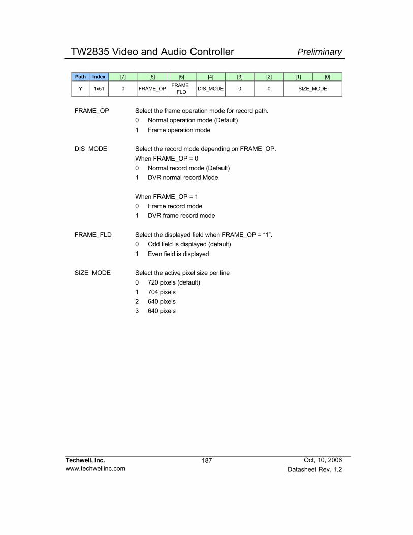
187
PreliminaryTW2835 Video and Audio Controller
Techwell, Inc. www.techwellinc.com Datasheet Rev. 1.2
Oct, 10, 2006
Path Index [7] [6] [5] [4] [3] [2] [1] [0]
Y 1x51 0 FRAME_OP FRAME_ FLD
DIS_MODE 0 0 SIZE_MODE
FRAME_OP Select the frame operation mode for record path. 0 Normal operation mode (Default) 1 Frame operation mode DIS_MODE Select the record mode depending on FRAME_OP. When FRAME_OP = 0 0 Normal record mode (Default) 1 DVR normal record Mode When FRAME_OP = 1 0 Frame record mode 1 DVR frame record mode FRAME_FLD Select the displayed field when FRAME_OP = “1”. 0 Odd field is displayed (default) 1 Even field is displayed SIZE_MODE Select the active pixel size per line 0 720 pixels (default) 1 704 pixels 2 640 pixels 3 640 pixels
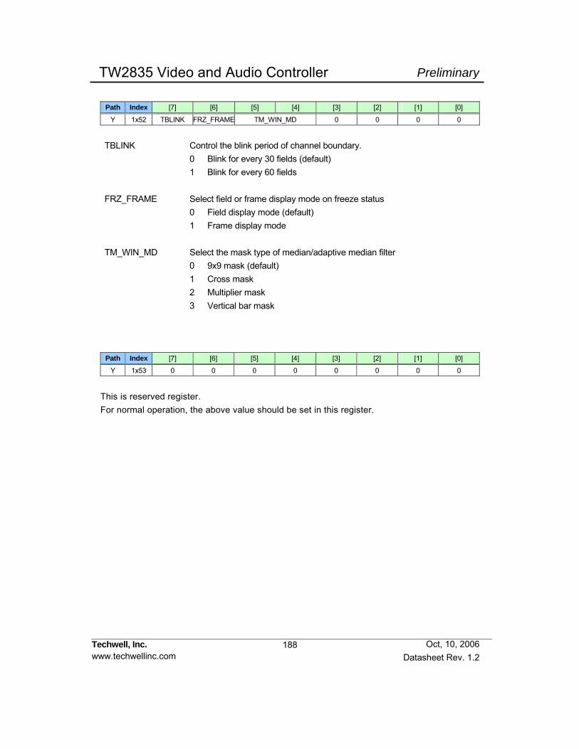
188
PreliminaryTW2835 Video and Audio Controller
Techwell, Inc. www.techwellinc.com Datasheet Rev. 1.2
Oct, 10, 2006
Path Index [7] [6] [5] [4] [3] [2] [1] [0]
Y 1x52 TBLINK FRZ_FRAME TM_WIN_MD 0 0 0 0
TBLINK Control the blink period of channel boundary. 0 Blink for every 30 fields (default) 1 Blink for every 60 fields
FRZ_FRAME Select field or frame display mode on freeze status 0 Field display mode (default) 1 Frame display mode TM_WIN_MD Select the mask type of median/adaptive median filter 0 9x9 mask (default) 1 Cross mask 2 Multiplier mask 3 Vertical bar mask
Path Index [7] [6] [5] [4] [3] [2] [1] [0]
Y 1x53 0 0 0 0 0 0 0 0
This is reserved register. For normal operation, the above value should be set in this register.

189
PreliminaryTW2835 Video and Audio Controller
Techwell, Inc. www.techwellinc.com Datasheet Rev. 1.2
Oct, 10, 2006
Path Index [7] [6] [5] [4] [3] [2] [1] [0]
Y 1x54 0 STRB_FLD DUAL_PAGE STRB_REQ
STRB_FLD Control the field mode for strobe operation. 0 Capture odd field only (default) 1 Capture even field only 2 Capture first field of any field 3 Capture frame DUAL_PAGE Enable dual page operation. 0 Normal strobe operation for each channel (default) 1 Enable the dual page operation STRB_REQ Request the strobe operation. STRB_REQ[3:0] represents the channel 3 to 0 0 None operation (default) 1 Request to start strobe operation

190
PreliminaryTW2835 Video and Audio Controller
Techwell, Inc. www.techwellinc.com Datasheet Rev. 1.2
Oct, 10, 2006
Path Index [7] [6] [5] [4] [3] [2] [1] [0]
Y 1x55 NOVID_MODE 0 CH_START 0 AUTO_NR_EN
INVALID_MODE
NOVID_MODE Select the indication method for no video detected channel 0 Bypass (default) 1 Capture last image 2 Blanked with blank color 3 Capture last image and blink channel boundary CH_START Enable the digital channel ID in horizontal boundary of channel 0 Disable the digital channel ID in horizontal boundary (default) 1 Enable the digital channel ID in horizontal boundary AUTO_NR_EN Enable the noise reduction filter automatically when night is detected 0 Disable auto noise reduction filter operation (default) 1 Enable auto noise reduction filter operation INVALID_MODE Select the indication mode for no channel area In horizontal and vertical active region 0 Background layer with background color (default) 1 Y = 0, Cb/Cr = 128 2 Y/Cb/Cr = 0 3 Y/Cb/Cr = 0
In horizontal and vertical blanking region 0 Y = 16, Cb/Cr = 128 (default) 1 Background layer with background color 2 Y = 0, Cb = 0, F, V, 0, Cascade, linenum[8:7], Cr = 0, linenum[6:0] 3 Y/Cb/Cr = 0
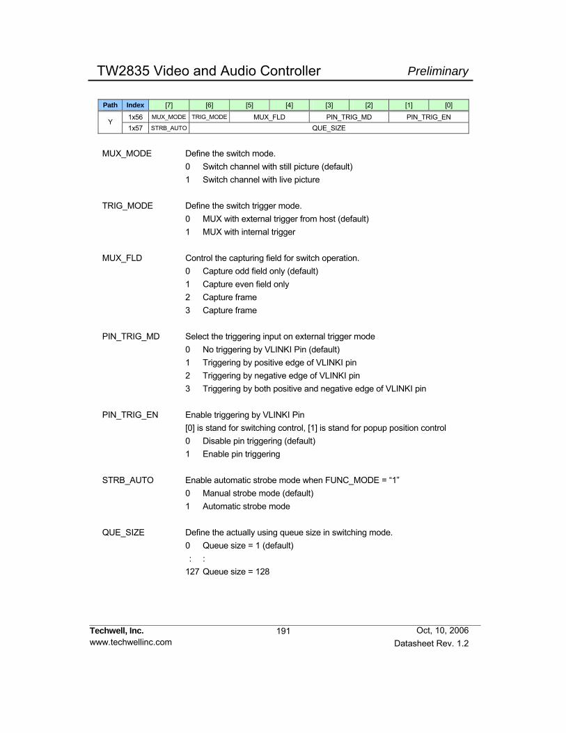
191
PreliminaryTW2835 Video and Audio Controller
Techwell, Inc. www.techwellinc.com Datasheet Rev. 1.2
Oct, 10, 2006
Path Index [7] [6] [5] [4] [3] [2] [1] [0]
1x56 MUX_MODE TRIG_MODE MUX_FLD PIN_TRIG_MD PIN_TRIG_EN Y
1x57 STRB_AUTO QUE_SIZE
MUX_MODE Define the switch mode. 0 Switch channel with still picture (default) 1 Switch channel with live picture TRIG_MODE Define the switch trigger mode. 0 MUX with external trigger from host (default) 1 MUX with internal trigger MUX_FLD Control the capturing field for switch operation. 0 Capture odd field only (default) 1 Capture even field only 2 Capture frame 3 Capture frame PIN_TRIG_MD Select the triggering input on external trigger mode 0 No triggering by VLINKI Pin (default) 1 Triggering by positive edge of VLINKI pin 2 Triggering by negative edge of VLINKI pin 3 Triggering by both positive and negative edge of VLINKI pin PIN_TRIG_EN Enable triggering by VLINKI Pin [0] is stand for switching control, [1] is stand for popup position control 0 Disable pin triggering (default) 1 Enable pin triggering STRB_AUTO Enable automatic strobe mode when FUNC_MODE = “1” 0 Manual strobe mode (default) 1 Automatic strobe mode
QUE_SIZE Define the actually using queue size in switching mode. 0 Queue size = 1 (default) : : 127 Queue size = 128

192
PreliminaryTW2835 Video and Audio Controller
Techwell, Inc. www.techwellinc.com Datasheet Rev. 1.2
Oct, 10, 2006
Path Index [7] [6] [5] [4] [3] [2] [1] [0]
1x58 QUE_PERIOD [7:0] Y
1x59 QUE_PERIOD [9:8] EXT_TRIG INTR_REQ MUX_WR_CH
QUE_PERIOD Control the trigger period for internal trigger mode. 0 Trigger period = 1 field (default) : : 1023 Trigger period = 1024 fields EXT_TRIG Make trigger when TRIG_MODE = “0” (external trigger mode). 0 None operation (default) 1 Request to start MUX with external trigger mode INTR_REQ Request to start the switch operation by interrupt 0 None operation (default) 1 Request to start the switch operation by interrupt MUX_WR_CH Define the channel number to be written in internal MUX queue or in
interrupt trigger. MUX_WR_CH[3:2] stands for stage of cascaded chips 0 Master chip (default) 1 1st slaver chip 2 2nd slaver chip 3 3rd slaver chip MUX_WR_CH[1:0] stands for channel number 0 Channel 0 (default) 1 Channel 1 2 Channel 2 3 Channel 3
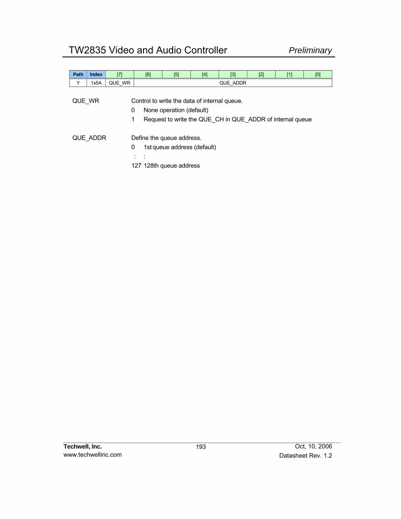
193
PreliminaryTW2835 Video and Audio Controller
Techwell, Inc. www.techwellinc.com Datasheet Rev. 1.2
Oct, 10, 2006
Path Index [7] [6] [5] [4] [3] [2] [1] [0]
Y 1x5A QUE_WR QUE_ADDR
QUE_WR Control to write the data of internal queue. 0 None operation (default) 1 Request to write the QUE_CH in QUE_ADDR of internal queue QUE_ADDR Define the queue address. 0 1st queue address (default) : : 127 128th queue address
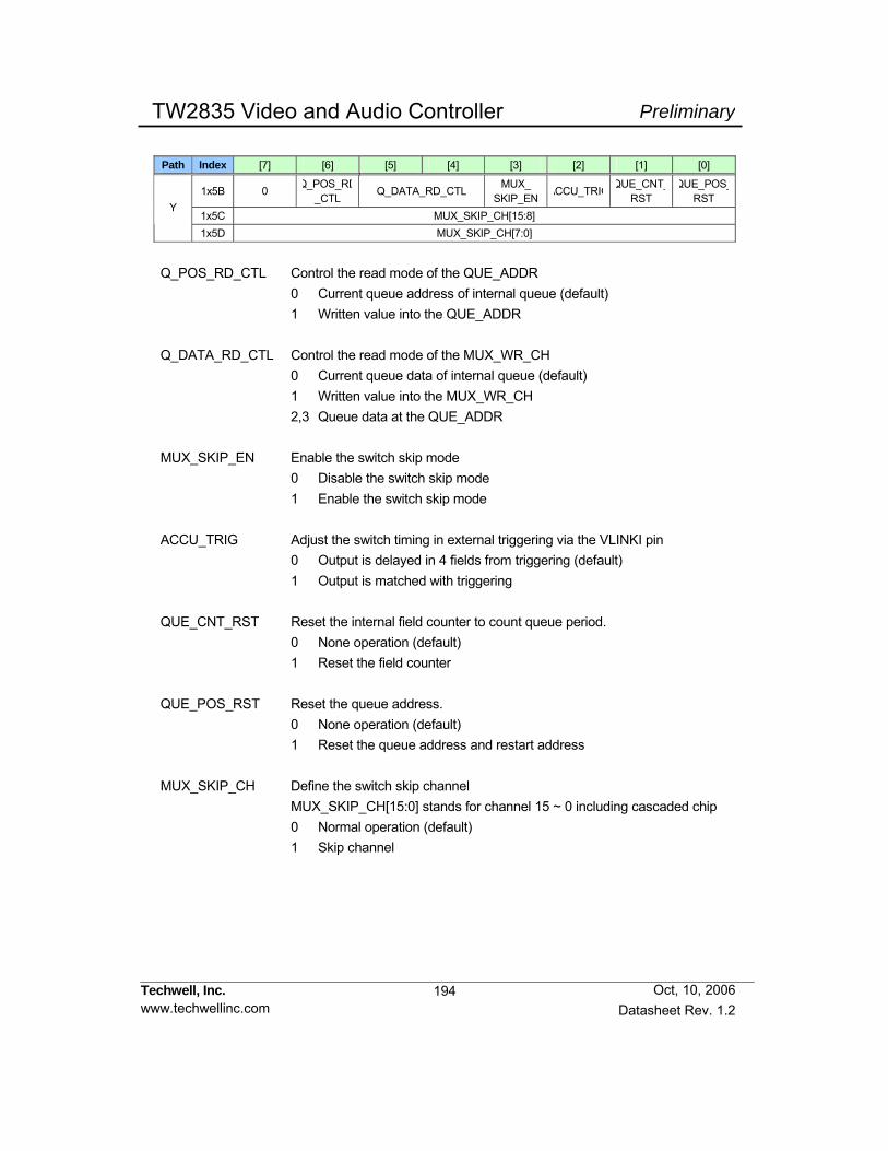
194
PreliminaryTW2835 Video and Audio Controller
Techwell, Inc. www.techwellinc.com Datasheet Rev. 1.2
Oct, 10, 2006
Path Index [7] [6] [5] [4] [3] [2] [1] [0]
1x5B 0 Q_POS_RD _CTL
Q_DATA_RD_CTL MUX_ SKIP_EN
ACCU_TRIG QUE_CNT_ RST
QUE_POS_RST
1x5C MUX_SKIP_CH[15:8] Y
1x5D MUX_SKIP_CH[7:0]
Q_POS_RD_CTL Control the read mode of the QUE_ADDR 0 Current queue address of internal queue (default) 1 Written value into the QUE_ADDR Q_DATA_RD_CTL Control the read mode of the MUX_WR_CH 0 Current queue data of internal queue (default) 1 Written value into the MUX_WR_CH 2,3 Queue data at the QUE_ADDR MUX_SKIP_EN Enable the switch skip mode 0 Disable the switch skip mode 1 Enable the switch skip mode ACCU_TRIG Adjust the switch timing in external triggering via the VLINKI pin 0 Output is delayed in 4 fields from triggering (default) 1 Output is matched with triggering QUE_CNT_RST Reset the internal field counter to count queue period. 0 None operation (default) 1 Reset the field counter QUE_POS_RST Reset the queue address. 0 None operation (default) 1 Reset the queue address and restart address MUX_SKIP_CH Define the switch skip channel MUX_SKIP_CH[15:0] stands for channel 15 ~ 0 including cascaded chip 0 Normal operation (default) 1 Skip channel
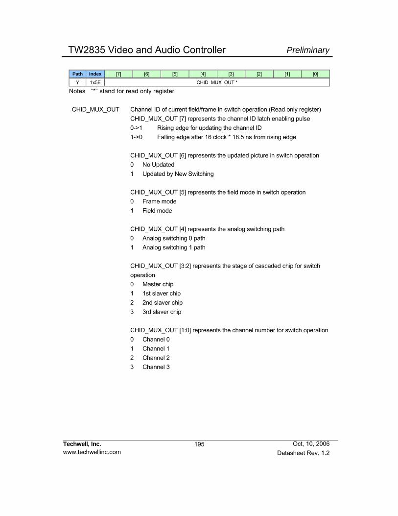
195
PreliminaryTW2835 Video and Audio Controller
Techwell, Inc. www.techwellinc.com Datasheet Rev. 1.2
Oct, 10, 2006
Path Index [7] [6] [5] [4] [3] [2] [1] [0]
Y 1x5E CHID_MUX_OUT *
Notes “*” stand for read only register CHID_MUX_OUT Channel ID of current field/frame in switch operation (Read only register) CHID_MUX_OUT [7] represents the channel ID latch enabling pulse 0->1 Rising edge for updating the channel ID 1->0 Falling edge after 16 clock * 18.5 ns from rising edge CHID_MUX_OUT [6] represents the updated picture in switch operation 0 No Updated 1 Updated by New Switching CHID_MUX_OUT [5] represents the field mode in switch operation 0 Frame mode 1 Field mode CHID_MUX_OUT [4] represents the analog switching path 0 Analog switching 0 path 1 Analog switching 1 path CHID_MUX_OUT [3:2] represents the stage of cascaded chip for switch operation 0 Master chip 1 1st slaver chip 2 2nd slaver chip 3 3rd slaver chip CHID_MUX_OUT [1:0] represents the channel number for switch operation 0 Channel 0 1 Channel 1 2 Channel 2 3 Channel 3

196
PreliminaryTW2835 Video and Audio Controller
Techwell, Inc. www.techwellinc.com Datasheet Rev. 1.2
Oct, 10, 2006
Path Index [7] [6] [5] [4] [3] [2] [1] [0]
Y 1x5F FRZ_FLD BNDCOL BGDCOL BLKCOL
FRZ_FLD Select the image for freeze function or for last capturing mode on video loss. 0 Last image (default) 1 Last image of 1 field before 2 Last image of 2 fields before 3 Last image of 3 fields before BNDCOL Define the boundary color of channel. 0 0% Black 1 25% Gray 2 75% Gray 3 100% White (default) Channel boundary color is changed according to this value when boundary
is blinking. 0 100% White 1 100% White 2 0% Black 3 0% Black (default) BGDCOL Define the background color. 0 0% Black 1 40% Gray (default) 2 75% Gray 3 100% Amplitude 100% Saturation Blue BLKCOL Define the color of the blanked channel. 0 0% Black 1 40% Gray 2 75% Gray 3 100% Amplitude 100% Saturation Blue (default)

197
PreliminaryTW2835 Video and Audio Controller
Techwell, Inc. www.techwellinc.com Datasheet Rev. 1.2
Oct, 10, 2006
Path CH Index [7] [6] [5] [4] [3] [2] [1] [0]
0 1x60 1 1x63 2 1x66
Y
3 1x69
CH_EN POP_UP FUNC_MODE NR_EN_DM NR_EN DEC_PATH_Y
CH_EN Enable the channel. 0 Disable the channel (default) 1 Enable the channel POP_UP Enable the pop-up attribute. 0 Disable the pop-up attribute (default) 1 Enable the pop-up attribute FUNC_MODE Select the operation mode. 0 Live mode (default) 1 Strobe mode 2-3 Switch mode NR_EN Enable the noise reduction filter in main path with ANA_SW = 0 NR_EN_DM Enable the noise reduction filter in sub path with ANA_SW = 1 0 Disable the noise reduction filter (defaut) 1 Enable the noise reduction filter DEC_PATH_Y Select the video input for each channel. 0 Video input from internal video decoder on VIN0 pins (default) 1 Video input from internal video decoder on VIN1 pins 2 Video input from internal video decoder on VIN2 pins 3 Video input from internal video decoder on VIN3 pins
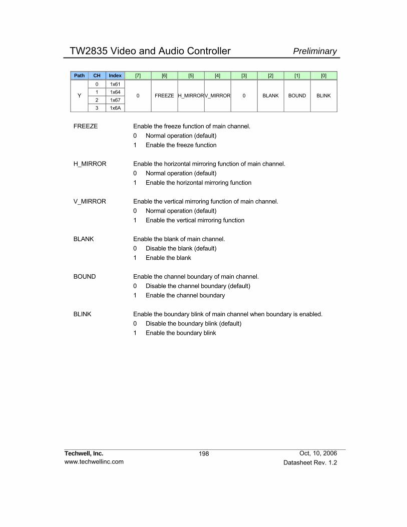
198
PreliminaryTW2835 Video and Audio Controller
Techwell, Inc. www.techwellinc.com Datasheet Rev. 1.2
Oct, 10, 2006
Path CH Index [7] [6] [5] [4] [3] [2] [1] [0]
0 1x61 1 1x64 2 1x67
Y
3 1x6A
0 FREEZE H_MIRRORV_MIRROR 0 BLANK BOUND BLINK
FREEZE Enable the freeze function of main channel. 0 Normal operation (default) 1 Enable the freeze function H_MIRROR Enable the horizontal mirroring function of main channel. 0 Normal operation (default) 1 Enable the horizontal mirroring function V_MIRROR Enable the vertical mirroring function of main channel. 0 Normal operation (default) 1 Enable the vertical mirroring function BLANK Enable the blank of main channel. 0 Disable the blank (default) 1 Enable the blank BOUND Enable the channel boundary of main channel. 0 Disable the channel boundary (default) 1 Enable the channel boundary BLINK Enable the boundary blink of main channel when boundary is enabled. 0 Disable the boundary blink (default) 1 Enable the boundary blink
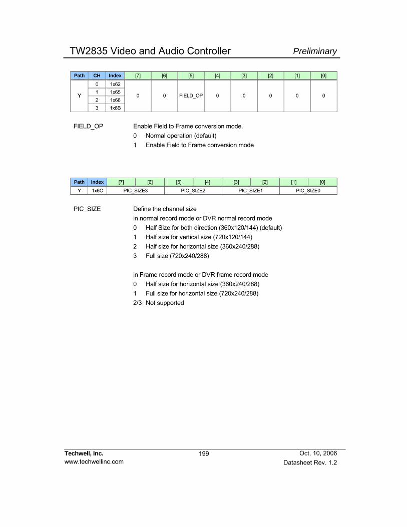
199
PreliminaryTW2835 Video and Audio Controller
Techwell, Inc. www.techwellinc.com Datasheet Rev. 1.2
Oct, 10, 2006
Path CH Index [7] [6] [5] [4] [3] [2] [1] [0]
0 1x62 1 1x65 2 1x68
Y
3 1x6B
0 0 FIELD_OP 0 0 0 0 0
FIELD_OP Enable Field to Frame conversion mode. 0 Normal operation (default) 1 Enable Field to Frame conversion mode Path Index [7] [6] [5] [4] [3] [2] [1] [0]
Y 1x6C PIC_SIZE3 PIC_SIZE2 PIC_SIZE1 PIC_SIZE0
PIC_SIZE Define the channel size in normal record mode or DVR normal record mode 0 Half Size for both direction (360x120/144) (default) 1 Half size for vertical size (720x120/144) 2 Half size for horizontal size (360x240/288) 3 Full size (720x240/288) in Frame record mode or DVR frame record mode 0 Half size for horizontal size (360x240/288) 1 Full size for horizontal size (720x240/288) 2/3 Not supported

200
PreliminaryTW2835 Video and Audio Controller
Techwell, Inc. www.techwellinc.com Datasheet Rev. 1.2
Oct, 10, 2006
Path Index [7] [6] [5] [4] [3] [2] [1] [0]
Y 1x6D PIC_POS3 PIC_POS2 PIC_POS1 PIC_POS0
PIC_POS Define the channel start position in Normal record mode 0 No offset for both horizontal and vertical direction (default) 1 Half offset for horizontal and no offset for vertical direction 2 No offset for horizontal and half offset for vertical direction 3 Half offset for horizontal and half offset for vertical direction in Frame record mode 0 No offset for both horizontal and vertical direction 1 Half offset for horizontal and no offset for vertical direction 2 No offset for horizontal and field offset for vertical direction 3 Half offset for horizontal and field offset for vertical direction in DVR normal record mode 0 No offset for both horizontal and vertical direction 1 Quarter offset for vertical direction 2 Half offset for vertical direction 3 Three Quarter offset for vertical direction in DVR Frame record mode 0 No offset for both horizontal and vertical direction 1 Half offset for vertical direction 2 Field offset for vertical direction 3 Field and half offset for vertical direction

201
PreliminaryTW2835 Video and Audio Controller
Techwell, Inc. www.techwellinc.com Datasheet Rev. 1.2
Oct, 10, 2006
Path Index [7] [6] [5] [4] [3] [2] [1] [0]
1x6E MUX_OUT_CH0 * MUX_OUT_CH1 * Y
1x6F MUX_OUT_CH2 * MUX_OUT_CH3 *
Notes “*” stand for read only register
MUX_OUT_CH0 Channel Information in current field/frame for switch operation MUX_OUT_CH1 Channel Information in next field/frame for switch operation MUX_OUT_CH2 Channel Information after 2 fields for switch operation MUX_OUT_CH3 Channel Information after 3 fields for switch operation MUX_OUT_CH [3:2] represents the stage of cascaded chips 0 Master chip (default) 1 1st slaver chip 2 2nd slaver chip 3 3rd slaver chip MUX_OUT_CH [1:0] represents the channel number 0 Channel 0 (default) 1 Channel 1 2 Channel 2 3 Channel 3

202
PreliminaryTW2835 Video and Audio Controller
Techwell, Inc. www.techwellinc.com Datasheet Rev. 1.2
Oct, 10, 2006
Path Index [7] [6] [5] [4] [3] [2] [1] [0]
Y 1x70 POS_CTL _EN
POS_TRIG _MODE
POS_TRIG POS_INTR 0 POS_RD _CTL
POS_DATA_RD_CTL
POS_CTL_EN Enable the position/popup control 0 Disable the position/popup control (default) 1 Enable the position/popup control POS_TRIG_MODE Select the position/popup trigger mode 0 External trigger mode (default) 1 Internal trigger mode POS_TRIG Request the external trigger on external trigger mode 0 None Operation (default) 1 Request to start position/popup control in external trigger mode POS_INTR Request to start position/popup control with interrupt 0 None Operation (default) 1 Request to start position/popup control with interrupt POS_RD_CTL Control the read mode for the POS_QUE_ADDR 0 Current queue address for internal position/popup queue (default) 1 Written value into the POS_QUE_ADDR POS_DATA_RD_CTL Control the read mode for the POS_CH 0 Current queue data for internal queue position (default) 1 Written POS_CH value 2 Queue data of the POS_QUE_ADDR 3 Queue data of the POS_QUE_ADDR

203
PreliminaryTW2835 Video and Audio Controller
Techwell, Inc. www.techwellinc.com Datasheet Rev. 1.2
Oct, 10, 2006
Path Index [7] [6] [5] [4] [3] [2] [1] [0]
1x71 POS_QUE_PER[9:8] POS_FLD_ MD POS_QUE_SIZE
1x72 POS_QUE_PER [7:0] 1x73 POS_CH0 POS_CH1
Y
1x74 POS_CH2 POS_CH3
POS_QUE_SIZE Control the position/popup queue size 0 Queue size = 1 (default) : : 31 Queue size = 32 POS_FLD_MD Select the position/popup queue period unit 0 Frame (default) 1 Field POS_QUE_PER Control the trigger period for internal trigger mode. 0 Trigger period = 1 field or frame (default) : : 1023 Trigger period = 1024 fields or frames
POS_CH Define the channel for each region POS_CH0 stands for no offset region of both H/V POS_CH1 stands for half offset of H POS_CH2 stands for half offset of V POS_CH3 stands for half offset of both H/V POS_CH [3:2] stands for the stage of cascaded chips 0 Master chip (default) 1 1st slaver chip 2 2nd slaver chip 3 3rd slaver chip POS_CH [1:0] stands for the channel number 0 Channel 0 (default) 1 Channel 1 2 Channel 2 3 Channel 3
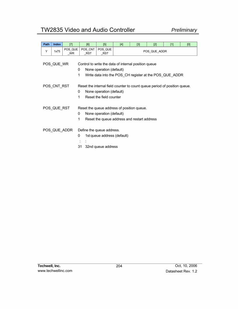
204
PreliminaryTW2835 Video and Audio Controller
Techwell, Inc. www.techwellinc.com Datasheet Rev. 1.2
Oct, 10, 2006
Path Index [7] [6] [5] [4] [3] [2] [1] [0]
Y 1x75 POS_QUE _WR
POS_CNT _RST
POS_QUE_RST
POS_QUE_ADDR
POS_QUE_WR Control to write the data of internal position queue 0 None operation (default) 1 Write data into the POS_CH register at the POS_QUE_ADDR POS_CNT_RST Reset the internal field counter to count queue period of position queue. 0 None operation (default) 1 Reset the field counter POS_QUE_RST Reset the queue address of position queue. 0 None operation (default) 1 Reset the queue address and restart address POS_QUE_ADDR Define the queue address. 0 1st queue address (default) : : 31 32nd queue address

205
PreliminaryTW2835 Video and Audio Controller
Techwell, Inc. www.techwellinc.com Datasheet Rev. 1.2
Oct, 10, 2006
Index [7] [6] [5] [4] [3] [2] [1] [0]
1x76 IRQENA_RD 0 0 0 0 0 IRQ_POL IRQ_RPT 1x77 IRQ_PERIOD
IRQENA_RD Select the read mode for IRQENA_XX registers 0 Read the Status/Event information (default) IRQ event will be cleared after host reads IRQENA_XX registers. 1 Read the written data IRQ event is not cleared even if host reads IRQENA_XX registers. IRQ_POL Select the IRQ polarity. 0 Active high (default) 1 Active low IRQ_RPT Select the IRQ mode. 0 IRQ pin maintains the state “1” until the interrupt request is cleared (default) 1 Interrupt request is repeated with 5msec period via IRQ pin when the interrupt is not cleared in long time. IRQ_PERIOD Control the interrupt generation period (The unit is field). 0 Immediate generation of interrupt when any Interrupt happens : : 255 Interrupt generation by the duration of the IRQ_PERIOD Index [7] [6] [5] [4] [3] [2] [1] [0]
1x78 IRQENA_NOVID
IRQENA_NOVID Enable the interrupt for video loss detection. IRQENA_NOVID[3:0] stand for VIN3 to VIN0 with ANMA_SW = 0 IRQENA_NOVID[7:4] stand for VIN3 to VIN0 with ANMA_SW = 1 0 Video-loss interrupt is disabled (default) 1 Video-loss interrupt is enabled The read information is determined by the IRQENA_RD (1x76). When the
IRQ_ENA_RD = “0”, the information is like the following and the interrupt will be cleared when the register is read by host.
0 Video is alive (default) 1 Video loss is detected
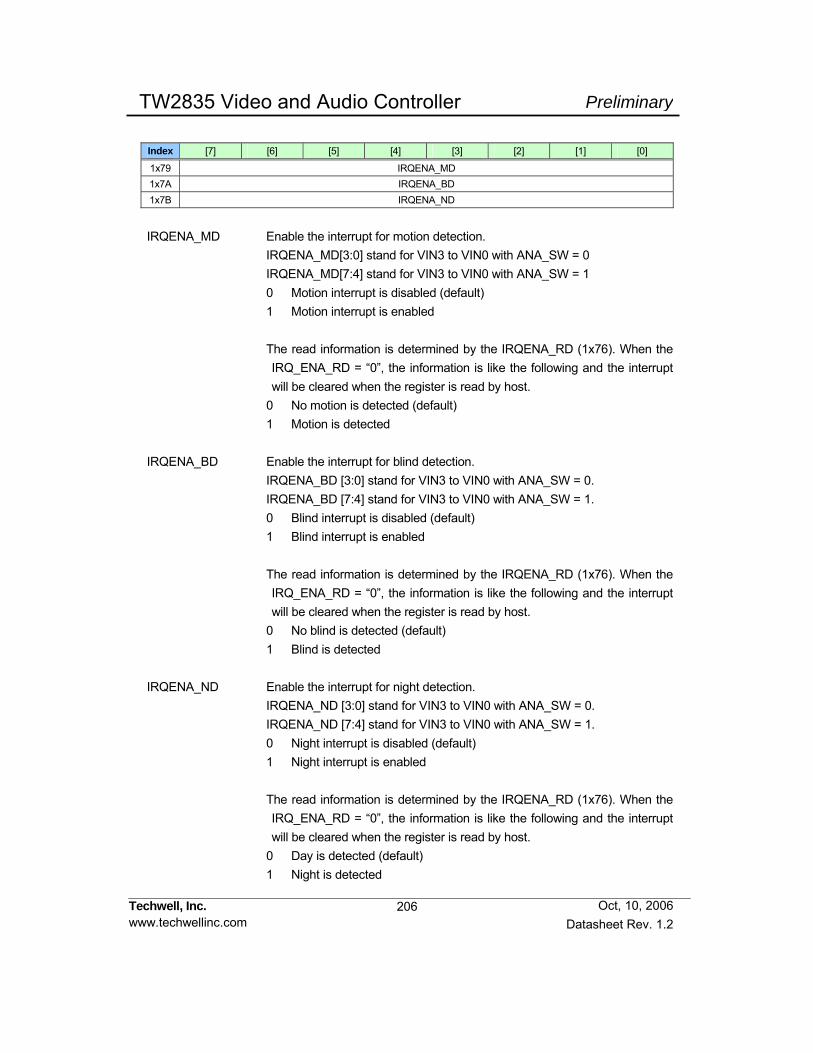
206
PreliminaryTW2835 Video and Audio Controller
Techwell, Inc. www.techwellinc.com Datasheet Rev. 1.2
Oct, 10, 2006
Index [7] [6] [5] [4] [3] [2] [1] [0]
1x79 IRQENA_MD 1x7A IRQENA_BD 1x7B IRQENA_ND
IRQENA_MD Enable the interrupt for motion detection. IRQENA_MD[3:0] stand for VIN3 to VIN0 with ANA_SW = 0 IRQENA_MD[7:4] stand for VIN3 to VIN0 with ANA_SW = 1 0 Motion interrupt is disabled (default) 1 Motion interrupt is enabled The read information is determined by the IRQENA_RD (1x76). When the
IRQ_ENA_RD = “0”, the information is like the following and the interrupt will be cleared when the register is read by host.
0 No motion is detected (default) 1 Motion is detected IRQENA_BD Enable the interrupt for blind detection. IRQENA_BD [3:0] stand for VIN3 to VIN0 with ANA_SW = 0. IRQENA_BD [7:4] stand for VIN3 to VIN0 with ANA_SW = 1. 0 Blind interrupt is disabled (default) 1 Blind interrupt is enabled
The read information is determined by the IRQENA_RD (1x76). When the IRQ_ENA_RD = “0”, the information is like the following and the interrupt will be cleared when the register is read by host.
0 No blind is detected (default) 1 Blind is detected
IRQENA_ND Enable the interrupt for night detection. IRQENA_ND [3:0] stand for VIN3 to VIN0 with ANA_SW = 0. IRQENA_ND [7:4] stand for VIN3 to VIN0 with ANA_SW = 1. 0 Night interrupt is disabled (default) 1 Night interrupt is enabled
The read information is determined by the IRQENA_RD (1x76). When the IRQ_ENA_RD = “0”, the information is like the following and the interrupt will be cleared when the register is read by host.
0 Day is detected (default) 1 Night is detected

207
PreliminaryTW2835 Video and Audio Controller
Techwell, Inc. www.techwellinc.com Datasheet Rev. 1.2
Oct, 10, 2006
Index [7] [6] [5] [4] [3] [2] [1] [0]
1x7C PB_NOVID_DET* 0 0 0 0
Notes “*” stand for read only register PB_NOVID_DET Status for playback input 0 Playback input is alive 1 Video-loss is detected for playback input
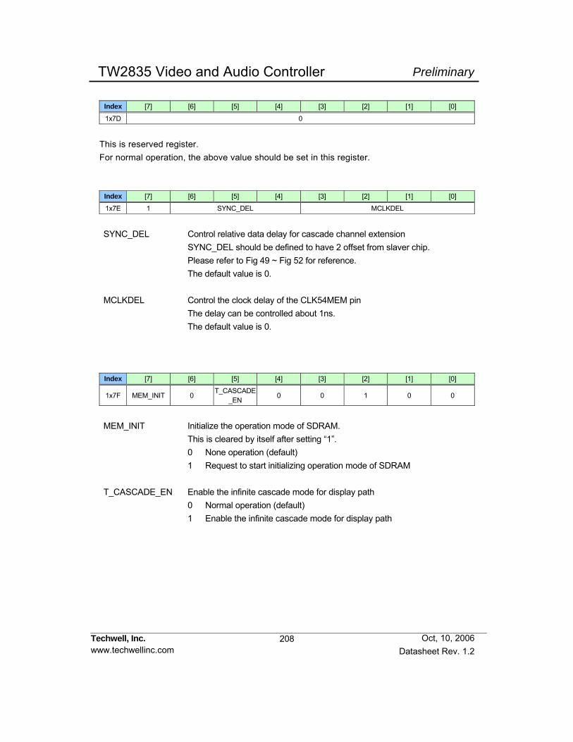
208
PreliminaryTW2835 Video and Audio Controller
Techwell, Inc. www.techwellinc.com Datasheet Rev. 1.2
Oct, 10, 2006
Index [7] [6] [5] [4] [3] [2] [1] [0]
1x7D 0
This is reserved register. For normal operation, the above value should be set in this register. Index [7] [6] [5] [4] [3] [2] [1] [0]
1x7E 1 SYNC_DEL MCLKDEL
SYNC_DEL Control relative data delay for cascade channel extension SYNC_DEL should be defined to have 2 offset from slaver chip. Please refer to Fig 49 ~ Fig 52 for reference. The default value is 0. MCLKDEL Control the clock delay of the CLK54MEM pin The delay can be controlled about 1ns. The default value is 0. Index [7] [6] [5] [4] [3] [2] [1] [0]
1x7F MEM_INIT 0 T_CASCADE
_EN 0 0 1 0 0
MEM_INIT Initialize the operation mode of SDRAM. This is cleared by itself after setting “1”. 0 None operation (default) 1 Request to start initializing operation mode of SDRAM T_CASCADE_EN Enable the infinite cascade mode for display path 0 Normal operation (default) 1 Enable the infinite cascade mode for display path

209
PreliminaryTW2835 Video and Audio Controller
Techwell, Inc. www.techwellinc.com Datasheet Rev. 1.2
Oct, 10, 2006
Index [7] [6] [5] [4] [3] [2] [1] [0]
1x80 VIS_ENA VIS_AUTO_ EN
AUTO_RPT_EN
VIS_DET_EN VIS_USER_EN
VIS_CODE_EN
VIS_RIC_ EN
1
1x81 VIS_PIXEL_HOS
VIS_ENA Enable the Analog channel ID during vertical blanking interval 0 Disable the Analog channel ID (default) 1 Enable the Analog channel ID VIS_AUTO_EN Enable the Auto channel ID In Analog channel ID 0 Disable the Auto channel ID (default) 1 Enable the Auto channel ID AUTO_RPT_EN Enable the Auto channel ID repetition mode in Analog channel ID 0 Disable the Auto channel ID repetition mode (default) 1 Enable the Auto channel ID repetition mode VIS_DET_EN Enable the Detection channel ID in Analog channel ID 0 Disable the Detection channel ID (default) 1 Enable the Detection channel ID VIS_USER_EN Enable the User channel ID in Analog channel ID 0 Disable the User channel ID (default) 1 Enable the User channel ID VIS_CODE_EN Enable the Digital channel ID 0 Disable the Digital channel ID (default) 1 Enable the Digital channel ID VIS_RIC_EN Enable the run-in clock of Analog channel ID during VBI 0 Disable the run-in clock (default) 1 Enable the run-in clock VIS_PIXEL_HOS Define the horizontal starting offset for Analog channel ID 0 No offset (default) : :
Table 1 255 pixel Offset

210
PreliminaryTW2835 Video and Audio Controller
Techwell, Inc. www.techwellinc.com Datasheet Rev. 1.2
Oct, 10, 2006
Index [7] [6] [5] [4] [3] [2] [1] [0]
1x82 VIS_FLD_OS 0 VIS_PIXEL_WIDTH 1x83 0 VIS_DM_MD 0 VIS_LINE_OS 1x84 VIS_HIGH_VAL 1x85 VIS_LOW_VAL
VIS_FLD_OS Control the vertical starting offset of each field for Analog channel ID 0 Odd : 1 Line, Even : 0 Line (default) 1 Odd : 1 Line, Even : 1 Line 2 Odd : 1 Line, Even : 2 Line 3 Odd : 1 Line, Even : 3 Line VIS_DM_MD Select the non-realtime mode for Detection channel ID 0 Normal mode (default) 1 Non-realtime Mode VIS_PIXEL_WIDTH Control the pixel width of each bit for Analog channel ID 0 1 pixel : : 31 32 pixels (default) VBI_LINE_OS Control the vertical starting offset from field transition for Analog channel ID 0 No offset : : 8 7 lines (default) : :
Table 1 31 lines VIS_HIGH_VAL Magnitude value for bit “1” of Analog channel ID (default = 235) VIS_LOW_VAL Magnitude value for bit “0” of Analog channel ID (default = 16)
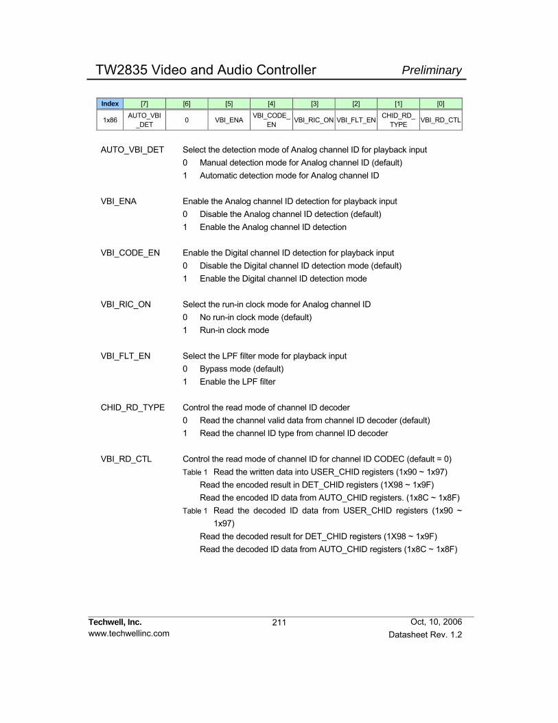
211
PreliminaryTW2835 Video and Audio Controller
Techwell, Inc. www.techwellinc.com Datasheet Rev. 1.2
Oct, 10, 2006
Index [7] [6] [5] [4] [3] [2] [1] [0]
1x86 AUTO_VBI _DET
0 VBI_ENA VBI_CODE_EN
VBI_RIC_ON VBI_FLT_EN CHID_RD_ TYPE
VBI_RD_CTL
AUTO_VBI_DET Select the detection mode of Analog channel ID for playback input 0 Manual detection mode for Analog channel ID (default) 1 Automatic detection mode for Analog channel ID VBI_ENA Enable the Analog channel ID detection for playback input 0 Disable the Analog channel ID detection (default) 1 Enable the Analog channel ID detection VBI_CODE_EN Enable the Digital channel ID detection for playback input 0 Disable the Digital channel ID detection mode (default) 1 Enable the Digital channel ID detection mode VBI_RIC_ON Select the run-in clock mode for Analog channel ID 0 No run-in clock mode (default) 1 Run-in clock mode VBI_FLT_EN Select the LPF filter mode for playback input 0 Bypass mode (default) 1 Enable the LPF filter CHID_RD_TYPE Control the read mode of channel ID decoder 0 Read the channel valid data from channel ID decoder (default) 1 Read the channel ID type from channel ID decoder VBI_RD_CTL Control the read mode of channel ID for channel ID CODEC (default = 0)
Table 1 Read the written data into USER_CHID registers (1x90 ~ 1x97) Read the encoded result in DET_CHID registers (1X98 ~ 1x9F) Read the encoded ID data from AUTO_CHID registers. (1x8C ~ 1x8F)
Table 1 Read the decoded ID data from USER_CHID registers (1x90 ~ 1x97)
Read the decoded result for DET_CHID registers (1X98 ~ 1x9F) Read the decoded ID data from AUTO_CHID registers (1x8C ~ 1x8F)
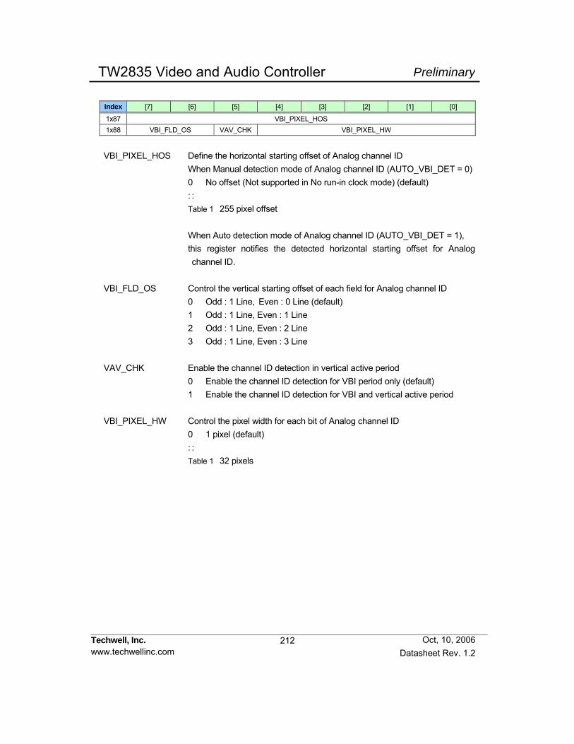
212
PreliminaryTW2835 Video and Audio Controller
Techwell, Inc. www.techwellinc.com Datasheet Rev. 1.2
Oct, 10, 2006
Index [7] [6] [5] [4] [3] [2] [1] [0]
1x87 VBI_PIXEL_HOS 1x88 VBI_FLD_OS VAV_CHK VBI_PIXEL_HW
VBI_PIXEL_HOS Define the horizontal starting offset of Analog channel ID When Manual detection mode of Analog channel ID (AUTO_VBI_DET = 0) 0 No offset (Not supported in No run-in clock mode) (default) : :
Table 1 255 pixel offset When Auto detection mode of Analog channel ID (AUTO_VBI_DET = 1), this register notifies the detected horizontal starting offset for Analog
channel ID. VBI_FLD_OS Control the vertical starting offset of each field for Analog channel ID 0 Odd : 1 Line, Even : 0 Line (default) 1 Odd : 1 Line, Even : 1 Line 2 Odd : 1 Line, Even : 2 Line 3 Odd : 1 Line, Even : 3 Line VAV_CHK Enable the channel ID detection in vertical active period 0 Enable the channel ID detection for VBI period only (default) 1 Enable the channel ID detection for VBI and vertical active period VBI_PIXEL_HW Control the pixel width for each bit of Analog channel ID 0 1 pixel (default) : :
Table 1 32 pixels

213
PreliminaryTW2835 Video and Audio Controller
Techwell, Inc. www.techwellinc.com Datasheet Rev. 1.2
Oct, 10, 2006
Index [7] [6] [5] [4] [3] [2] [1] [0]
1x89 VBI_LINE_WIDTH VBI_LINE_OS 1x8A VBI_MID_VAL 1x8B CHID_TYPE/CHID_VALID *
Notes “*” stand for read only register VBI_LINE_WIDTH Control the line width for Analog channel ID When Manual detection mode of Analog channel ID (AUTO_VBI_DET = 0) 0 1 line : :
Table 1 8 lines (default) When Auto detection mode of Analog channel ID (AUTO_VBI_DET = 1), this register notifies the detected line width for Analog channel ID. VBI_LINE_OS Control the vertical starting offset from field transition for Analog channel ID 0 No offset : : 8 7 lines (default) : :
Table 1 31 lines VBI_MID_VAL Define the threshold level to detect bit “0” or bit “1” from Analog channel ID (default = 128) CHID_VALID Status for validity of detected channel ID when CHID_RD_TYPE = 0 CHID_VALID[4] stands for Auto Channel ID CHID_VALID[3] stands for Detection Channel ID 0 CHID_VALID[2] stands for Detection Channel ID 1 CHID_VALID[1] stands for User Channel ID 0 CHID_VALID[0] stands for User Channel ID 1 0 Not Valid 1 Valid CHID_TYPE Indication of the detected channel ID type when CHID_RD_TYPE = 1 CHID_TYPE[5:0] stands for line number for Analog channel ID 0 Auto channel ID 1 User/Detection channel ID
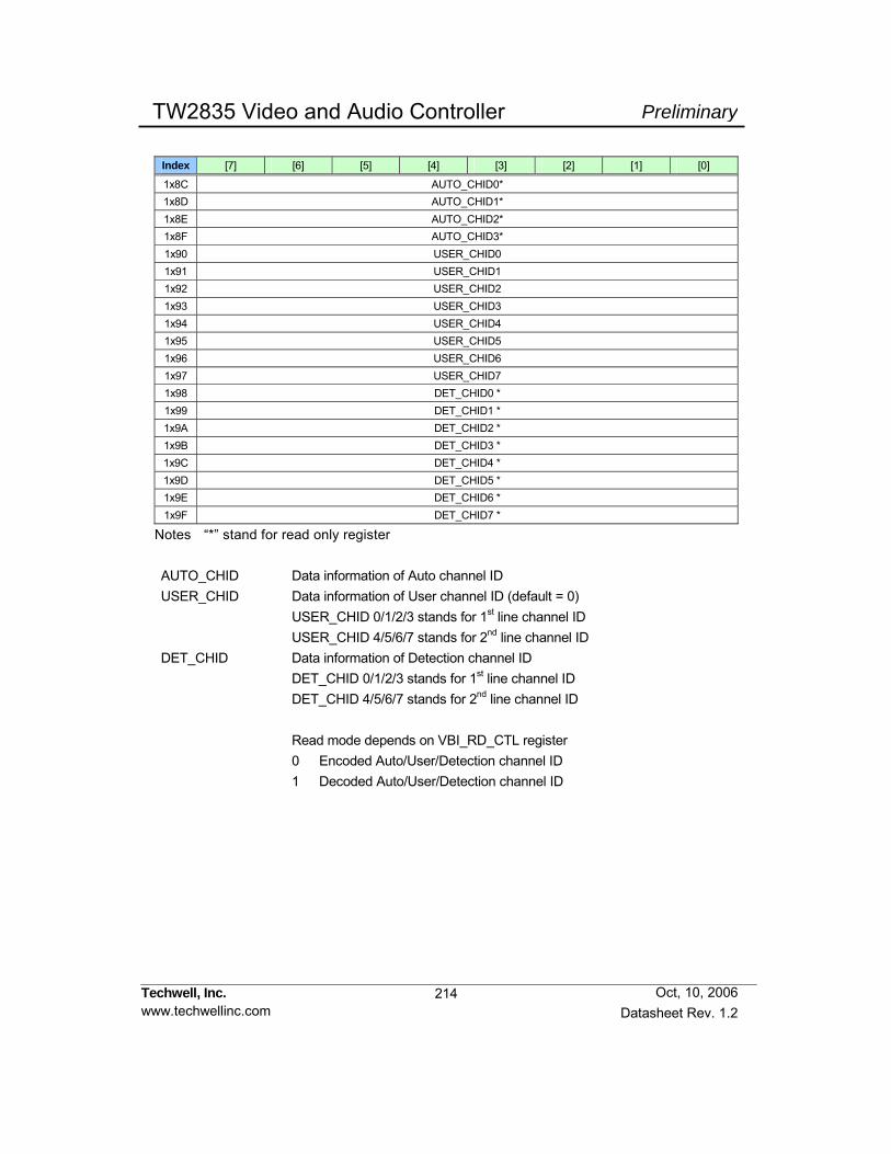
214
PreliminaryTW2835 Video and Audio Controller
Techwell, Inc. www.techwellinc.com Datasheet Rev. 1.2
Oct, 10, 2006
Index [7] [6] [5] [4] [3] [2] [1] [0]
1x8C AUTO_CHID0* 1x8D AUTO_CHID1* 1x8E AUTO_CHID2* 1x8F AUTO_CHID3* 1x90 USER_CHID0 1x91 USER_CHID1 1x92 USER_CHID2 1x93 USER_CHID3 1x94 USER_CHID4 1x95 USER_CHID5 1x96 USER_CHID6 1x97 USER_CHID7 1x98 DET_CHID0 * 1x99 DET_CHID1 * 1x9A DET_CHID2 * 1x9B DET_CHID3 * 1x9C DET_CHID4 * 1x9D DET_CHID5 * 1x9E DET_CHID6 * 1x9F DET_CHID7 *
Notes “*” stand for read only register AUTO_CHID Data information of Auto channel ID USER_CHID Data information of User channel ID (default = 0) USER_CHID 0/1/2/3 stands for 1st line channel ID USER_CHID 4/5/6/7 stands for 2nd line channel ID DET_CHID Data information of Detection channel ID DET_CHID 0/1/2/3 stands for 1st line channel ID DET_CHID 4/5/6/7 stands for 2nd line channel ID Read mode depends on VBI_RD_CTL register 0 Encoded Auto/User/Detection channel ID 1 Decoded Auto/User/Detection channel ID

215
PreliminaryTW2835 Video and Audio Controller
Techwell, Inc. www.techwellinc.com Datasheet Rev. 1.2
Oct, 10, 2006
Index [7] [6] [5] [4] [3] [2] [1] [0]
1xA0 ENC_IN_X ENC_IN_Y CCIR_IN_X CCIR_IN_Y
ENC_IN Select the video data for analog output of video encoder. 0 Video data of display path without OSD and mouse overlay (default) 1 Video data of display path with OSD and mouse overlay 2 Video data of record path without OSD and mouse overlay 3 Video data of record path with OSD and mouse overlay CCIR_IN Select the video data for ITU-R BT 656 digital output. 0 Video data of display path without OSD and mouse overlay (default) 1 Video data of display path with OSD and mouse overlay 2 Video data of record path without OSD and mouse overlay 3 Video data of record path with OSD and mouse overlay Index [7] [6] [5] [4] [3] [2] [1] [0]
1xA1 DAC_PD_CX 0 DAC_OUT_YX DAC_PD_YX 0 DAC_OUT_CX
DAC_PD_YX Enable the power down of VAOYX DAC. DAC_PD_CX Enable the power down of VAOCX DAC. 0 Normal operation (default) 1 Enable power down of DAC DAC_OUT_YX Define the analog video format for VAOYX DAC. DAC_OUT_CX Define the analog video format for VAOCX DAC. 0 No Output (default) 1 CVBS for display path 2 Luminance for display path 3 Chrominance for display path

216
PreliminaryTW2835 Video and Audio Controller
Techwell, Inc. www.techwellinc.com Datasheet Rev. 1.2
Oct, 10, 2006
Index [7] [6] [5] [4] [3] [2] [1] [0]
1xA2 1 DAC_OUT_YY DAC_PD_YY 0 0 0
DAC_PD_YY Enable the power down of VAOYY DAC. 0 Normal operation (default) 1 Enable power down of DAC DAC_OUT_YY Define the analog video format for VAOYY DAC. 0 No Output (default) 1 CVBS for display path 2 Not supported 3 Not supported 4 Not supported 5 CVBS for record path 6 Not supported 7 Not supported
Path Display Record Format No Output CVBS Luma Chroma CVBS
VAOYX O O O O X
VAOCX O O O O X Ouptput
VAOYY O O X X O
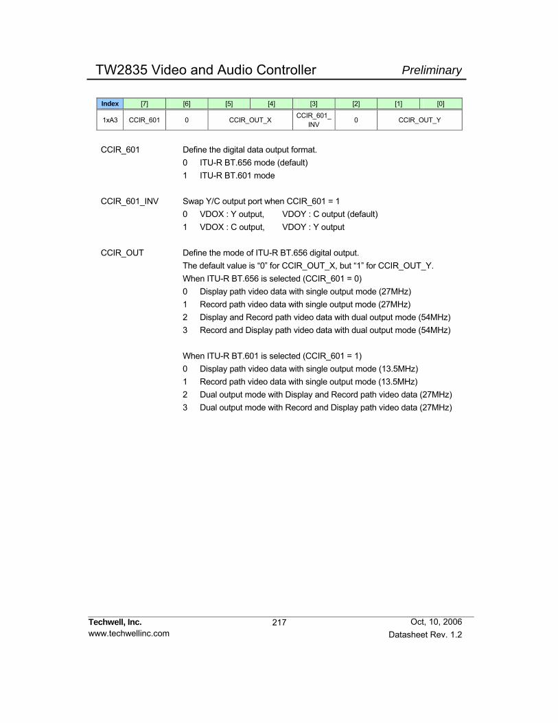
217
PreliminaryTW2835 Video and Audio Controller
Techwell, Inc. www.techwellinc.com Datasheet Rev. 1.2
Oct, 10, 2006
Index [7] [6] [5] [4] [3] [2] [1] [0]
1xA3 CCIR_601 0 CCIR_OUT_X CCIR_601_ INV
0 CCIR_OUT_Y
CCIR_601 Define the digital data output format. 0 ITU-R BT.656 mode (default) 1 ITU-R BT.601 mode
CCIR_601_INV Swap Y/C output port when CCIR_601 = 1 0 VDOX : Y output, VDOY : C output (default) 1 VDOX : C output, VDOY : Y output CCIR_OUT Define the mode of ITU-R BT.656 digital output. The default value is “0” for CCIR_OUT_X, but “1” for CCIR_OUT_Y. When ITU-R BT.656 is selected (CCIR_601 = 0) 0 Display path video data with single output mode (27MHz) 1 Record path video data with single output mode (27MHz) 2 Display and Record path video data with dual output mode (54MHz) 3 Record and Display path video data with dual output mode (54MHz)
When ITU-R BT.601 is selected (CCIR_601 = 1) 0 Display path video data with single output mode (13.5MHz) 1 Record path video data with single output mode (13.5MHz) 2 Dual output mode with Display and Record path video data (27MHz) 3 Dual output mode with Record and Display path video data (27MHz)
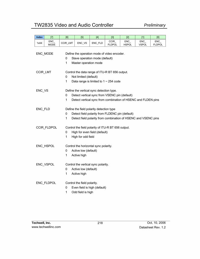
218
PreliminaryTW2835 Video and Audio Controller
Techwell, Inc. www.techwellinc.com Datasheet Rev. 1.2
Oct, 10, 2006
Index [7] [6] [5] [4] [3] [2] [1] [0]
1xA4 ENC_ MODE
CCIR_LMT ENC_VS ENC_FLD CCIR_ FLDPOL
ENC_ HSPOL
ENC_ VSPOL
ENC_ FLDPOL
ENC_MODE Define the operation mode of video encoder. 0 Slave operation mode (default) 1 Master operation mode CCIR_LMT Control the data range of ITU-R BT 656 output. 0 Not limited (default) 1 Data range is limited to 1 ~ 254 code ENC_VS Define the vertical sync detection type. 0 Detect vertical sync from VSENC pin (default) 1 Detect vertical sync from combination of HSENC and FLDEN pins ENC_FLD Define the field polarity detection type 0 Detect field polarity from FLDENC pin (default) 1 Detect field polarity from combination of HSENC and VSENC pins CCIR_FLDPOL Control the field polarity of ITU-R BT 656 output. 0 High for even field (default) 1 High for odd field ENC_HSPOL Control the horizontal sync polarity. 0 Active low (default) 1 Active high ENC_VSPOL Control the vertical sync polarity. 0 Active low (default) 1 Active high ENC_FLDPOL Control the field polarity. 0 Even field is high (default) 1 Odd field is high
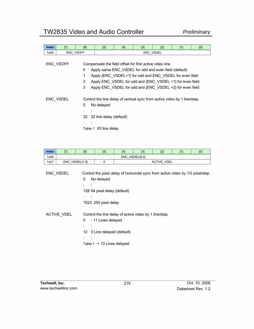
219
PreliminaryTW2835 Video and Audio Controller
Techwell, Inc. www.techwellinc.com Datasheet Rev. 1.2
Oct, 10, 2006
Index [7] [6] [5] [4] [3] [2] [1] [0]
1xA5 ENC_VSOFF ENC_VSDEL
ENC_VSOFF Compensate the field offset for first active video line. 0 Apply same ENC_VSDEL for odd and even field (default) 1 Apply ENC_VSDEL+1 for odd and ENC_VSDEL for even field 2 Apply ENC_VSDEL for odd and ENC_VSDEL +1 for even field 3 Apply ENC_VSDEL for odd and ENC_VSDEL +2 for even field ENC_VSDEL Control the line delay of vertical sync from active video by 1 line/step. 0 No delayed : : 32 32 line delay (default) : :
Table 1 63 line delay Index [7] [6] [5] [4] [3] [2] [1] [0]
1xA6 ENC_HSDEL[9:2] 1xA7 ENC_HSDEL[1:0] 0 ACTIVE_VDEL
ENC_HSDEL Control the pixel delay of horizontal sync from active video by 1/2 pixel/step. 0 No delayed : : 128 64 pixel delay (default) : : 1023 255 pixel delay ACTIVE_VDEL Control the line delay of active video by 1 line/step. 0 - 11 Lines delayed : : 12 0 Line delayed (default) : :
Table 1 + 13 Lines delayed
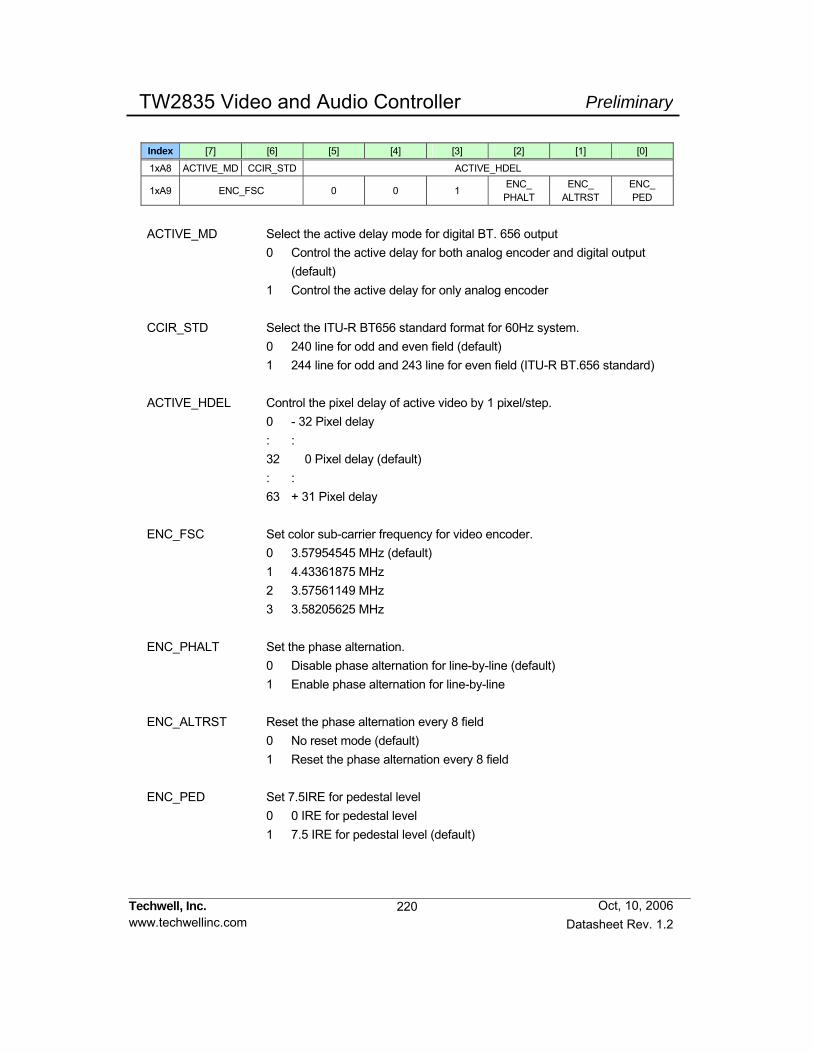
220
PreliminaryTW2835 Video and Audio Controller
Techwell, Inc. www.techwellinc.com Datasheet Rev. 1.2
Oct, 10, 2006
Index [7] [6] [5] [4] [3] [2] [1] [0]
1xA8 ACTIVE_MD CCIR_STD ACTIVE_HDEL
1xA9 ENC_FSC 0 0 1 ENC_ PHALT
ENC_ ALTRST
ENC_ PED
ACTIVE_MD Select the active delay mode for digital BT. 656 output 0 Control the active delay for both analog encoder and digital output (default) 1 Control the active delay for only analog encoder CCIR_STD Select the ITU-R BT656 standard format for 60Hz system. 0 240 line for odd and even field (default) 1 244 line for odd and 243 line for even field (ITU-R BT.656 standard)
ACTIVE_HDEL Control the pixel delay of active video by 1 pixel/step. 0 - 32 Pixel delay : : 32 0 Pixel delay (default) : : 63 + 31 Pixel delay ENC_FSC Set color sub-carrier frequency for video encoder. 0 3.57954545 MHz (default) 1 4.43361875 MHz 2 3.57561149 MHz 3 3.58205625 MHz ENC_PHALT Set the phase alternation. 0 Disable phase alternation for line-by-line (default) 1 Enable phase alternation for line-by-line ENC_ALTRST Reset the phase alternation every 8 field 0 No reset mode (default) 1 Reset the phase alternation every 8 field ENC_PED Set 7.5IRE for pedestal level 0 0 IRE for pedestal level 1 7.5 IRE for pedestal level (default)

221
PreliminaryTW2835 Video and Audio Controller
Techwell, Inc. www.techwellinc.com Datasheet Rev. 1.2
Oct, 10, 2006
Index [7] [6] [5] [4] [3] [2] [1] [0]
1xAA ENC_CBW_X ENC_YBW_X ENC_CBW_Y ENC_YBW_Y
ENC_CBW Control the chrominance bandwidth of video encoder. 0 0.8 MHz 1 1.15 MHz 2 1.35 MHz (default) 3 1.35 MHz ENC_YBW Control the luminance bandwidth of video encoder. 0 Narrow bandwidth 1 Narrower bandwidth 2 Wide bandwidth (default) 3 Middle band width
Index [7] [6] [5] [4] [3] [2] [1] [0]
1xAB 0 HOUT* VOUT* FOUT* ENC_
BAR_X ENC_
CKILL_X ENC_
BAR_Y ENC_
CKILL_Y
Notes “*” stand for read only register
HOUT Status of horizontal sync for encoder timing VOUT Status of vertical sync for encoder timing FOUT Status of field polarity for encoder timing ENC_BAR Enable the test pattern output. 0 Normal operation (default) 1 Internal color bar with 100% amplitude 100 % saturation ENC_CKILL Enable the color killing function 0 Normal operation (default) 1 Color is killed
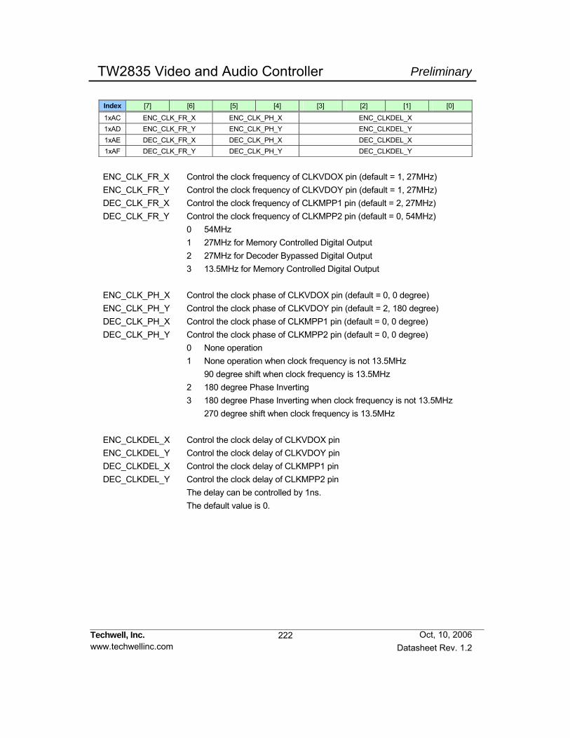
222
PreliminaryTW2835 Video and Audio Controller
Techwell, Inc. www.techwellinc.com Datasheet Rev. 1.2
Oct, 10, 2006
Index [7] [6] [5] [4] [3] [2] [1] [0]
1xAC ENC_CLK_FR_X ENC_CLK_PH_X ENC_CLKDEL_X 1xAD ENC_CLK_FR_Y ENC_CLK_PH_Y ENC_CLKDEL_Y 1xAE DEC_CLK_FR_X DEC_CLK_PH_X DEC_CLKDEL_X 1xAF DEC_CLK_FR_Y DEC_CLK_PH_Y DEC_CLKDEL_Y
ENC_CLK_FR_X Control the clock frequency of CLKVDOX pin (default = 1, 27MHz) ENC_CLK_FR_Y Control the clock frequency of CLKVDOY pin (default = 1, 27MHz) DEC_CLK_FR_X Control the clock frequency of CLKMPP1 pin (default = 2, 27MHz) DEC_CLK_FR_Y Control the clock frequency of CLKMPP2 pin (default = 0, 54MHz) 0 54MHz 1 27MHz for Memory Controlled Digital Output 2 27MHz for Decoder Bypassed Digital Output 3 13.5MHz for Memory Controlled Digital Output ENC_CLK_PH_X Control the clock phase of CLKVDOX pin (default = 0, 0 degree) ENC_CLK_PH_Y Control the clock phase of CLKVDOY pin (default = 2, 180 degree) DEC_CLK_PH_X Control the clock phase of CLKMPP1 pin (default = 0, 0 degree) DEC_CLK_PH_Y Control the clock phase of CLKMPP2 pin (default = 0, 0 degree) 0 None operation 1 None operation when clock frequency is not 13.5MHz 90 degree shift when clock frequency is 13.5MHz 2 180 degree Phase Inverting 3 180 degree Phase Inverting when clock frequency is not 13.5MHz 270 degree shift when clock frequency is 13.5MHz ENC_CLKDEL_X Control the clock delay of CLKVDOX pin ENC_CLKDEL_Y Control the clock delay of CLKVDOY pin DEC_CLKDEL_X Control the clock delay of CLKMPP1 pin DEC_CLKDEL_Y Control the clock delay of CLKMPP2 pin The delay can be controlled by 1ns. The default value is 0.

223
PreliminaryTW2835 Video and Audio Controller
Techwell, Inc. www.techwellinc.com Datasheet Rev. 1.2
Oct, 10, 2006
Index [7] [6] [5] [4] [3] [2] [1] [0]
1xB0 0 0 MPPOUT2 MPPOUT1 MPPOUT0 1xB1 MPPSET0_MSB MPPSET0_LSB 1xB2 MPPDATA0_MSB MPPDATA0_ LSB 1xB3 MPPSET1_MSB MPPSET1_ LSB 1xB4 MPPDATA1_MSB MPPDATA1_ LSB 1xB5 MPPSET2_ MSB MPPSET2_ LSB 1xB6 MPPDATA2_ MSB MPPDATA2_ LSB
MPPOUT2 Select the MPP2 pin function (default= 0) MPPOUT1 Select the MPP1 pin function (default= 0) MPPOUT0 Select the DLINKI pin function (default= 0) In cascaded mode, DLINKI pin is reserved for cascaded operation 0 Multi purpose output mode 1 (default) 1 GPPIO mode 2 Multi purpose output mode 2 MPPSET_MSB Select the function for MPP [7:4] pins in Multi purpose output Mod 1 Select I/O for each bit for MPP [7:4] pins in GPPIO Mode Select the function for MPP [7:4] pins in Multi purpose output Mod 2 (default= 0) MPPSET_LSB Select the function for MPP [3:0] pins in Multi purpose output Mod 1 Select I/O for each bit for MPP [3:0] pins in GPPIO Mode Select the function for MPP [3:0] pins in Multi purpose output Mod 2 (default= 0) The detailed description for each mode is shown in following table MPPDATA_MSB In writing mode, the data is for MPP [7:4] in GPPIO mode In reading mode, the data stands for MPP [7:4] pin status (default= 0) MPPDATA_LSB In writing mode, the data is for MPP [3:0] in GPPIO mode In reading mode, the data stands for MPP [3:0] pin status (default= 0)
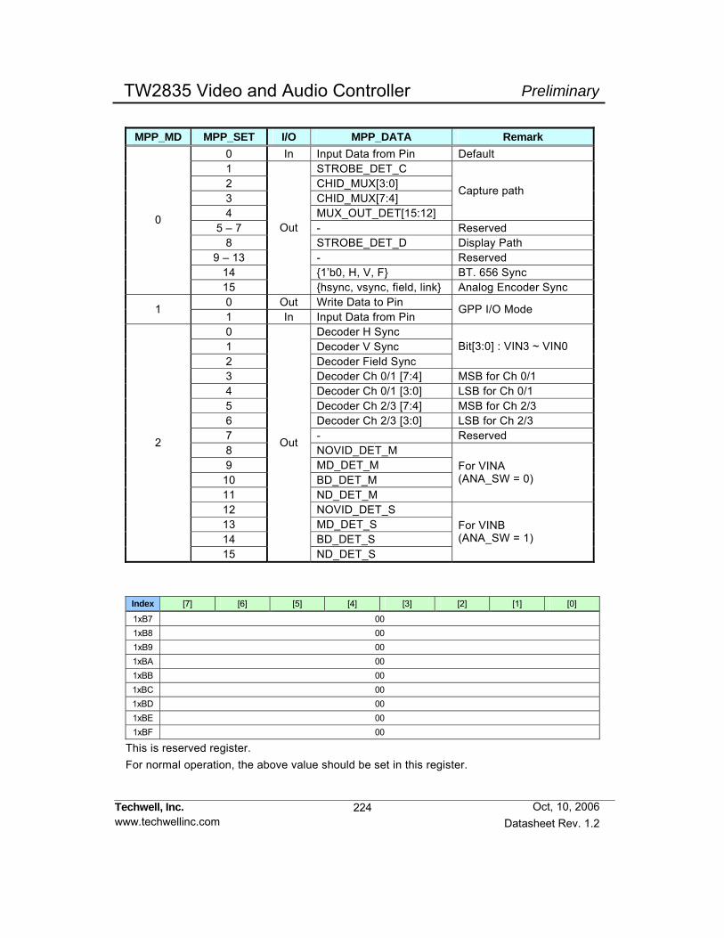
224
PreliminaryTW2835 Video and Audio Controller
Techwell, Inc. www.techwellinc.com Datasheet Rev. 1.2
Oct, 10, 2006
MPP_MD MPP_SET I/O MPP_DATA Remark
0 In Input Data from Pin Default 1 STROBE_DET_C 2 CHID_MUX[3:0] 3 CHID_MUX[7:4] 4 MUX_OUT_DET[15:12]
Capture path
5 – 7 - Reserved 8 STROBE_DET_D Display Path
9 – 13 - Reserved 14 1’b0, H, V, F BT. 656 Sync
0
15
Out
hsync, vsync, field, link Analog Encoder Sync 0 Out Write Data to Pin 1 1 In Input Data from Pin
GPP I/O Mode
0 Decoder H Sync 1 Decoder V Sync 2 Decoder Field Sync
Bit[3:0] : VIN3 ~ VIN0
3 Decoder Ch 0/1 [7:4] MSB for Ch 0/1 4 Decoder Ch 0/1 [3:0] LSB for Ch 0/1 5 Decoder Ch 2/3 [7:4] MSB for Ch 2/3 6 Decoder Ch 2/3 [3:0] LSB for Ch 2/3 7 - Reserved 8 NOVID_DET_M 9 MD_DET_M
10 BD_DET_M 11 ND_DET_M
For VINA (ANA_SW = 0)
12 NOVID_DET_S 13 MD_DET_S 14 BD_DET_S
2
15
Out
ND_DET_S
For VINB (ANA_SW = 1)
Index [7] [6] [5] [4] [3] [2] [1] [0]
1xB7 00 1xB8 00 1xB9 00 1xBA 00 1xBB 00 1xBC 00 1xBD 00 1xBE 00 1xBF 00
This is reserved register. For normal operation, the above value should be set in this register.

225
PreliminaryTW2835 Video and Audio Controller
Techwell, Inc. www.techwellinc.com Datasheet Rev. 1.2
Oct, 10, 2006
Index [7] [6] [5] [4] [3] [2] [1] [0]
2x00 OSD_BUF_DATA[31:24] 2x01 OSD_BUF_DATA[23:16] 2x02 OSD_BUF_DATA[15:8] 2x03 OSD_BUF_DATA[7:0]
2x04 OSD_BUF_ WR
OSD_BUF_ RD
0 OSD_BUF_ADDR
OSD_BUF_DATA Define the writing data of OSD buffer (Internal Buffer Size = 32Bit x 16) in
normal single writing mode Define the OSD acceleration data in acceleration downloading mode (default = 0) [31:24] is left top font from 4 OSD dot in display path [31:28] is left top font from 8 OSD dot in capture path Read mode depends on OSD_BUF_RD 0 Read the buffer data with OSD_BUF_ADDR (default) 1 Read the OSD acceleration downloading data OSD_BUF_WR Request to write the OSD internal buffer This bit is cleared automatically after downloading is finished 0 Disable the writing or Writing is finished (default) 1 Enable the writing OSD_BUF_ADDR Select the OSD internal buffer address to read/write 0 0 internal buffer address (default) : :
Table 1 15 internal buffer address
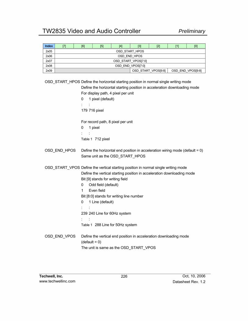
226
PreliminaryTW2835 Video and Audio Controller
Techwell, Inc. www.techwellinc.com Datasheet Rev. 1.2
Oct, 10, 2006
Index [7] [6] [5] [4] [3] [2] [1] [0]
2x05 OSD_START_HPOS 2x06 OSD_END_HPOS 2x07 OSD_START_VPOS[7:0] 2x08 OSD_END_VPOS[7:0] 2x09 OSD_START_VPOS[9:8] OSD_END_VPOS[9:8]
OSD_START_HPOS Define the horizontal starting position in normal single writing mode Define the horizontal starting position in acceleration downloading mode For display path, 4 pixel per unit 0 1 pixel (default) : : 179 716 pixel For record path, 8 pixel per unit 0 1 pixel : :
Table 1 712 pixel OSD_END_HPOS Define the horizontal end position in acceleration wiring mode (default = 0) Same unit as the OSD_START_HPOS OSD_START_VPOS Define the vertical starting position in normal single writing mode Define the vertical starting position in acceleration downloading mode Bit [9] stands for writing field 0 Odd field (default) 1 Even field Bit [8:0] stands for writing line number 0 1 Line (default) : : 239 240 Line for 60Hz system : :
Table 1 288 Line for 50Hz system OSD_END_VPOS Define the vertical end position in acceleration downloading mode (default = 0) The unit is same as the OSD_START_VPOS

227
PreliminaryTW2835 Video and Audio Controller
Techwell, Inc. www.techwellinc.com Datasheet Rev. 1.2
Oct, 10, 2006
Index [7] [6] [5] [4] [3] [2] [1] [0]
2x09 BUF_WR_SIZE
2x0A OSD_MEM_
WR OSD_ACC_
EN OSD_MEM_
PATH OSD_PAGE_D 0
INDEX_RD_MD
BUF_WR_SIZE Define the buffer downloading size in normal single writing mode 0 32 Bit X 1 (default) : :
Table 1 32 Bit X 16 OSD_MEM_WR Enable to write the OSD into memory. This bit is cleared automatically after downloading is finished 0 Disable the writing or Writing is finished (default) 1 Enable the writing OSD_ACC_EN Select the OSD writing mode 0 Normal single writing mode using internal buffer (default) 1 Acceleration downloading mode OSD_MEM_PATH Select the OSD writing Path 0 Display path (default) 1 Record path OSD_WR_PAGE Select OSD writing page for display path 0 Page = 0 (default) : :
Table 1 Page = 5 6/7 Not allowed
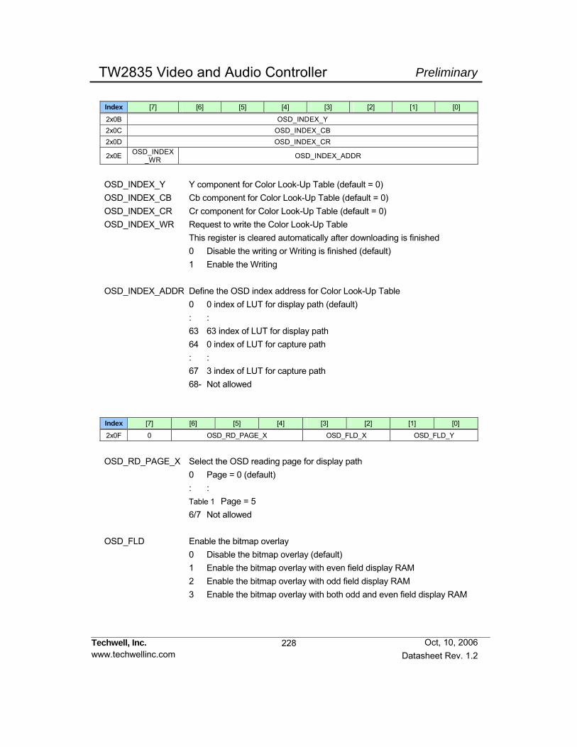
228
PreliminaryTW2835 Video and Audio Controller
Techwell, Inc. www.techwellinc.com Datasheet Rev. 1.2
Oct, 10, 2006
Index [7] [6] [5] [4] [3] [2] [1] [0]
2x0B OSD_INDEX_Y 2x0C OSD_INDEX_CB 2x0D OSD_INDEX_CR
2x0E OSD_INDEX _WR OSD_INDEX_ADDR
OSD_INDEX_Y Y component for Color Look-Up Table (default = 0) OSD_INDEX_CB Cb component for Color Look-Up Table (default = 0) OSD_INDEX_CR Cr component for Color Look-Up Table (default = 0) OSD_INDEX_WR Request to write the Color Look-Up Table This register is cleared automatically after downloading is finished 0 Disable the writing or Writing is finished (default) 1 Enable the Writing OSD_INDEX_ADDR Define the OSD index address for Color Look-Up Table 0 0 index of LUT for display path (default) : : 63 63 index of LUT for display path 64 0 index of LUT for capture path : : 67 3 index of LUT for capture path 68- Not allowed Index [7] [6] [5] [4] [3] [2] [1] [0]
2x0F 0 OSD_RD_PAGE_X OSD_FLD_X OSD_FLD_Y
OSD_RD_PAGE_X Select the OSD reading page for display path 0 Page = 0 (default) : :
Table 1 Page = 5 6/7 Not allowed OSD_FLD Enable the bitmap overlay 0 Disable the bitmap overlay (default) 1 Enable the bitmap overlay with even field display RAM 2 Enable the bitmap overlay with odd field display RAM 3 Enable the bitmap overlay with both odd and even field display RAM
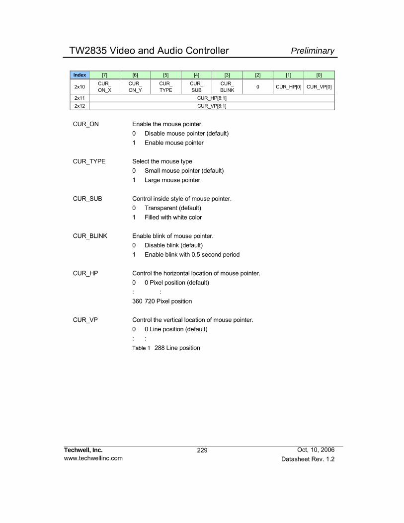
229
PreliminaryTW2835 Video and Audio Controller
Techwell, Inc. www.techwellinc.com Datasheet Rev. 1.2
Oct, 10, 2006
Index [7] [6] [5] [4] [3] [2] [1] [0]
2x10 CUR_ ON_X
CUR_ ON_Y
CUR_ TYPE
CUR_ SUB
CUR_ BLINK
0 CUR_HP[0] CUR_VP[0]
2x11 CUR_HP[8:1] 2x12 CUR_VP[8:1]
CUR_ON Enable the mouse pointer. 0 Disable mouse pointer (default) 1 Enable mouse pointer CUR_TYPE Select the mouse type 0 Small mouse pointer (default) 1 Large mouse pointer CUR_SUB Control inside style of mouse pointer. 0 Transparent (default) 1 Filled with white color CUR_BLINK Enable blink of mouse pointer. 0 Disable blink (default) 1 Enable blink with 0.5 second period CUR_HP Control the horizontal location of mouse pointer. 0 0 Pixel position (default) : : 360 720 Pixel position CUR_VP Control the vertical location of mouse pointer. 0 0 Line position (default) : :
Table 1 288 Line position

230
PreliminaryTW2835 Video and Audio Controller
Techwell, Inc. www.techwellinc.com Datasheet Rev. 1.2
Oct, 10, 2006
Index [7] [6] [5] [4] [3] [2] [1] [0]
2x13 CLUT0_Y 2x14 CLUT0_CB 2x15 CLUT0_CR 2x16 CLUT1_Y 2x17 CLUT1_CB 2x18 CLUT1_CR 2x19 CLUT2_Y 2x1A CLUT2_CB 2x1B CLUT2_CR 2x1C CLUT3_Y 2x1D CLUT3_CB 2x1E CLUT3_CR
CLUT0_Y Y component for user defined color 0 (default : 0) CLUT0_CB Cb component for user defined color 0 (default : 0) CLUT0_CR Cr component for user defined color 0 (default : 0) CLUT1_Y Y component for user defined color 1 (default : 0) CLUT1_CB Cb component for user defined color 1 (default : 0) CLUT1_CR Cr component for user defined color 1 (default : 0) CLUT2_Y Y component for user defined color 2 (default : 0) CLUT2_CB Cb component for user defined color 2 (default : 0) CLUT2_CR Cr component for user defined color 2 (default : 0) CLUT3_Y Y component for user defined color 3 (default : 0) CLUT3_CB Cb component for user defined color 3 (default : 0) CLUT3_CR Cr component for user defined color 3 (default : 0)
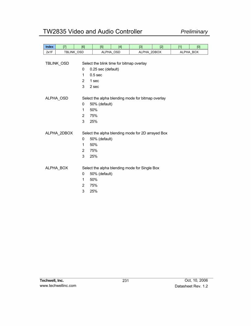
231
PreliminaryTW2835 Video and Audio Controller
Techwell, Inc. www.techwellinc.com Datasheet Rev. 1.2
Oct, 10, 2006
Index [7] [6] [5] [4] [3] [2] [1] [0]
2x1F TBLINK_OSD ALPHA_OSD ALPHA_2DBOX ALPHA_BOX
TBLINK_OSD Select the blink time for bitmap overlay 0 0.25 sec (default) 1 0.5 sec 2 1 sec 3 2 sec ALPHA_OSD Select the alpha blending mode for bitmap overlay 0 50% (default) 1 50% 2 75% 3 25% ALPHA_2DBOX Select the alpha blending mode for 2D arrayed Box 0 50% (default) 1 50% 2 75% 3 25% ALPHA_BOX Select the alpha blending mode for Single Box 0 50% (default) 1 50% 2 75% 3 25%

232
PreliminaryTW2835 Video and Audio Controller
Techwell, Inc. www.techwellinc.com Datasheet Rev. 1.2
Oct, 10, 2006
Box Index [7] [6] [5] [4] [3] [2] [1] [0]
B0 2x20 B1 2x26 B2 2x2B B3 2x32
BOX_BND_COL BOX_
PLNMIX_YBOX_
BNDEN_YBOX_
PLNEN_Y BOX_
PLNMIX_XBOX_
BNDEN_X BOX_
PLNEN_X
BOX_BND_COL Define the box boundary color for each box 0 0% White (Default) 1 25% White 2 50% White 3 75% White BOX_PLNMIX_Y Enable the alpha blending for box plane area in record path 0 No alpha blending (Default) 1 Enable alpha blending BOX_BNDEN_Y Enable the box boundary in record path 0 Disable (Default) 1 Enable BOX_PLNEN_Y Enable the box plane area in record path 0 Disable (Default) 1 Enable BOX_PLNMIX_X Enable the alpha blending of box plane area in display path 0 No alpha blending (Default) 1 Enable alpha blending BOX_BNDEN_X Enable the box boundary in display path 0 Disable (Default) 1 Enable BOX_PLNEN_X Enable the box plane area in display path 0 Disable (Default) 1 Enable

233
PreliminaryTW2835 Video and Audio Controller
Techwell, Inc. www.techwellinc.com Datasheet Rev. 1.2
Oct, 10, 2006
Box Index [7] [6] [5] [4] [3] [2] [1] [0]
B0 2x21 B1 2x27 B2 2x2C B3 2x33
BOX_PLNCOL
BOX_PLNCOL Define the box plane color for each box 0 White (75% Amplitude 100% Saturation) (default) 1 Yellow (75% Amplitude 100% Saturation) 2 Cyan (75 % Amplitude 100 Saturation) 3 Green (75% Amplitude 100% Saturation) 4 Magenta (75% Amplitude 100% Saturation) 5 Red (75% Amplitude 100% Saturation) 6 Blue (75% Amplitude 100% Saturation) 7 0% Black 8 100% White 9 50% Gray 10 25% Gray 11 Blue (75% Amplitude 75% Saturation) 12 Defined by CLUT0 13 Defined by CLUT1 14 Defined by CLUT2 15 Defined by CLUT3
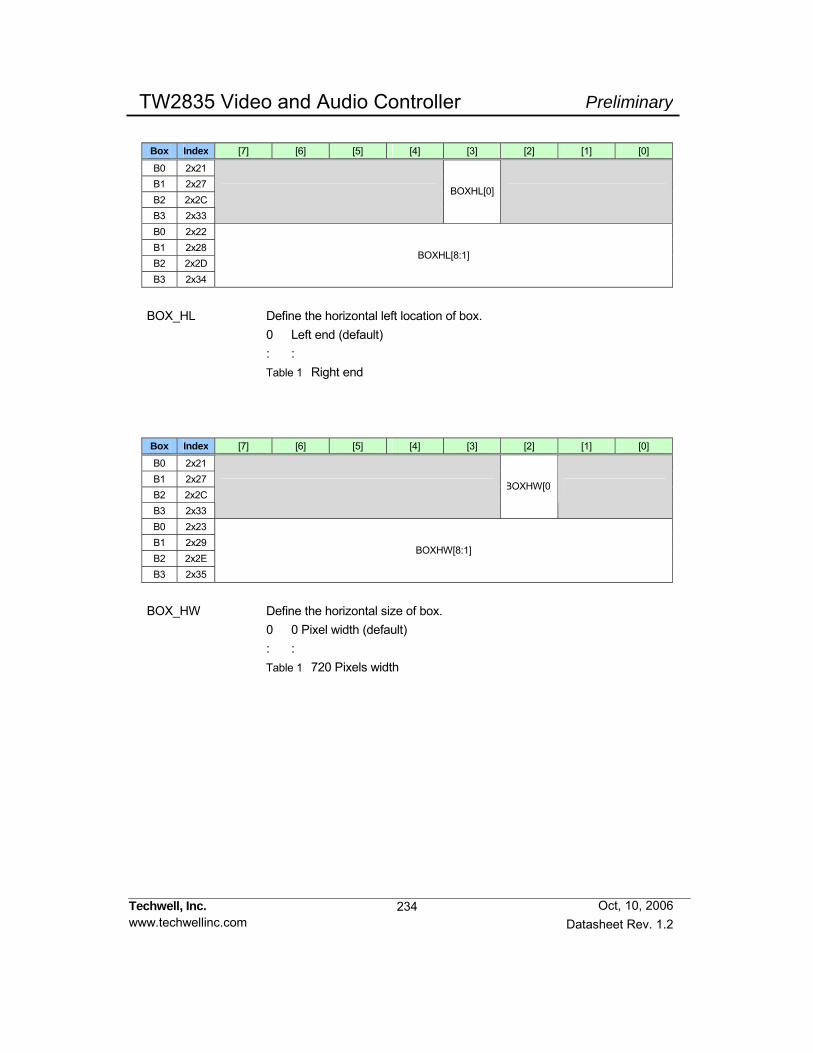
234
PreliminaryTW2835 Video and Audio Controller
Techwell, Inc. www.techwellinc.com Datasheet Rev. 1.2
Oct, 10, 2006
Box Index [7] [6] [5] [4] [3] [2] [1] [0]
B0 2x21 B1 2x27 B2 2x2C B3 2x33
BOXHL[0]
B0 2x22 B1 2x28 B2 2x2D B3 2x34
BOXHL[8:1]
BOX_HL Define the horizontal left location of box. 0 Left end (default) : :
Table 1 Right end Box Index [7] [6] [5] [4] [3] [2] [1] [0]
B0 2x21 B1 2x27 B2 2x2C B3 2x33
BOXHW[0]
B0 2x23 B1 2x29 B2 2x2E B3 2x35
BOXHW[8:1]
BOX_HW Define the horizontal size of box. 0 0 Pixel width (default) : :
Table 1 720 Pixels width

235
PreliminaryTW2835 Video and Audio Controller
Techwell, Inc. www.techwellinc.com Datasheet Rev. 1.2
Oct, 10, 2006
Box Index [7] [6] [5] [4] [3] [2] [1] [0]
B0 2x21 B1 2x27 B2 2x2C B3 2x33
BOXVT[0]
B0 2x24 B1 2x2A B2 2x2F B3 2x36
BOXVT[8:1]
BOX_VT Define the vertical top location of box. 0 Vertical top (default) : :
Table 1 Vertical bottom Box Index [7] [6] [5] [4] [3] [2] [1] [0]
B0 2x21 B1 2x27 B2 2x2C B3 2x33
BOXVW[0]
B0 2x25 B1 2x2B B2 2x30 B3 2x37
BOXVW[8:1]
BOX_VW Define the vertical size of box. 0 0 Lines height (default) : :
Table 1 288 Lines height
Index [7] [6] [5] [4] [3] [2] [1] [0]
2x38 0 0 OSD_OVL_MD_D OSD_OVL_MD_C
OSD_OVL_MD Control the OSD overlay mode for each path 0 No overlay (default) 1 Enable overlay with high priority 2 Enable overlay with low priority 3 Enable overlay with no priority

236
PreliminaryTW2835 Video and Audio Controller
Techwell, Inc. www.techwellinc.com Datasheet Rev. 1.2
Oct, 10, 2006
2DBox Index [7] [6] [5] [4] [3] [2] [1] [0]
2DB0 2x5B 2DB1 2x5C 2DB2 2x5D 2DB3 2x5E
MDAREA_COL DETAREA_COL
2x5F MDBND3_COL MDBND2_COL MDBND1_COL MDBND0_COL
MDAREA_COL Define the color of Mask plane in 2D arrayed box. (default = 0) DETAREA_COL Define the color of Detection plane in 2D arrayed box. (default = 0) 0 White (75% Amplitude 100% Saturation) 1 Yellow (75% Amplitude 100% Saturation) 2 Cyan (75 % Amplitude 100 Saturation) 3 Green (75% Amplitude 100% Saturation) 4 Magenta (75% Amplitude 100% Saturation) 5 Red (75% Amplitude 100% Saturation) 6 Blue (75% Amplitude 100% Saturation) 7 0% Black 8 100% White 9 50% Gray 10 25% Gray 11 Blue (75% Amplitude 75% Saturation) 12 Defined by CLUT0 13 Defined by CLUT1 14 Defined by CLUT2 15 Defined by CLUT3 MDBND_COL Define the color of 2D arrayed box boundary 0 0 % Black (default) 1 25% Gray 2 50% Gray 3 75% White Define the displayed color for cursor cell and motion-detected region 0,1 75% White (default) 2,3 0% Black

237
PreliminaryTW2835 Video and Audio Controller
Techwell, Inc. www.techwellinc.com Datasheet Rev. 1.2
Oct, 10, 2006
2Dbox Index [7] [6] [5] [4] [3] [2] [1] [0]
2DB0 2x60 2DB1 2x68 2DB2 2x70 2DB3 2x78
2DBOX _EN_X
2DBOX _EN_Y
2DBOX _MODE
2DBOX_ CUREN
2DBOX _MIX 2DBOX_IN_SEL
2DBOX_EN Enable the 2Dbox 0 Disable the 2D box (default) 1 Enable the 2D box 2DBOX_MODE Define the operation mode of 2D arrayed box. 0 Table mode (default) 1 Motion display mode 2DBOX_CUREN Enable the cursor cell inside 2D arrayed box. 0 Disable the cursor cell (default) 1 Enable the cursor cell 2DBOX_MIX Enable the alpha blending for 2D arrayed box plane with video data. 0 Disable the alpha blending (default) 1 Enable the alpha blending with ALPHA_2DBOX setting (2x03) 2DBOX_IN_SEL Select the input for Mask / Detection data of 2D Box. 0 Mask and Detection Data for VIN 0 and ANA_SW = 0 (default) 1 Mask and Detection Data for VIN1 and ANA_SW = 0 2 Mask and Detection Data for VIN 2 and ANA_SW = 0 3 Mask and Detection Data for VIN 3 and ANA_SW = 0 4 Mask and Detection Data for VIN 0 and ANA_SW = 1 5 Mask and Detection Data for VIN1 and ANA_SW = 1 6 Mask and Detection Data for VIN 2 and ANA_SW = 1 7 Mask and Detection Data for VIN 3 and ANA_SW = 1
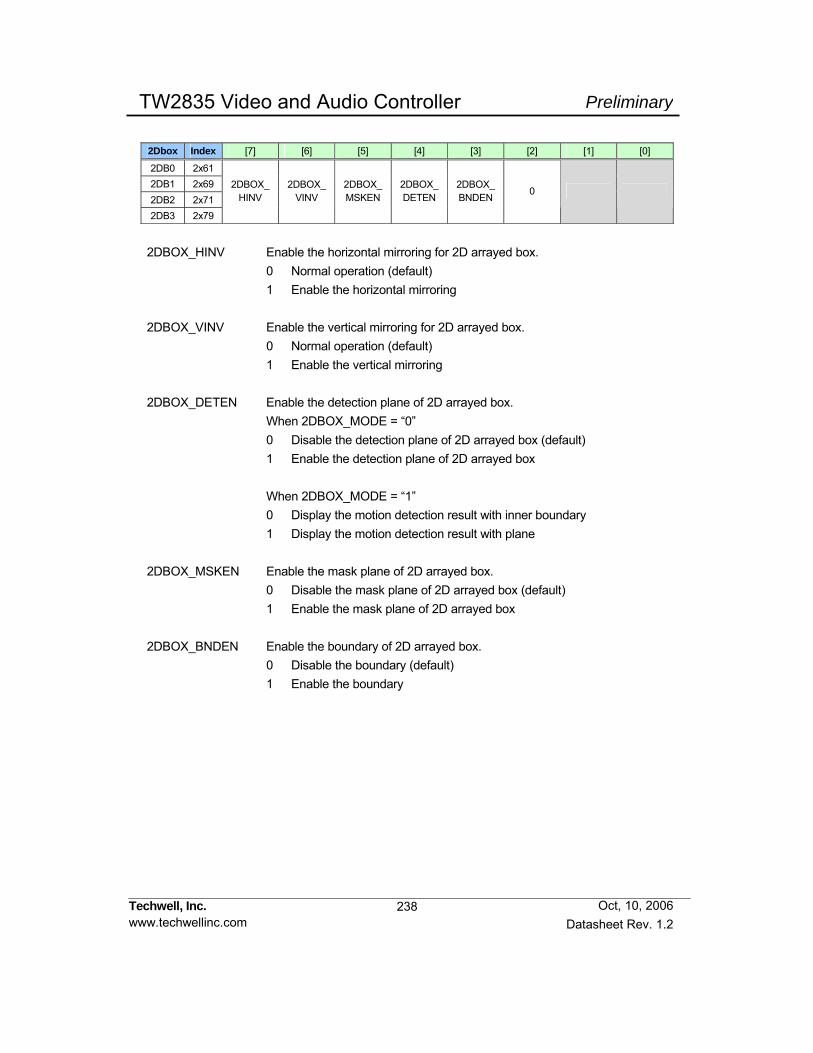
238
PreliminaryTW2835 Video and Audio Controller
Techwell, Inc. www.techwellinc.com Datasheet Rev. 1.2
Oct, 10, 2006
2Dbox Index [7] [6] [5] [4] [3] [2] [1] [0]
2DB0 2x61 2DB1 2x69 2DB2 2x71 2DB3 2x79
2DBOX_ HINV
2DBOX_ VINV
2DBOX_ MSKEN
2DBOX_ DETEN
2DBOX_ BNDEN 0
2DBOX_HINV Enable the horizontal mirroring for 2D arrayed box. 0 Normal operation (default) 1 Enable the horizontal mirroring 2DBOX_VINV Enable the vertical mirroring for 2D arrayed box. 0 Normal operation (default) 1 Enable the vertical mirroring 2DBOX_DETEN Enable the detection plane of 2D arrayed box. When 2DBOX_MODE = “0” 0 Disable the detection plane of 2D arrayed box (default) 1 Enable the detection plane of 2D arrayed box When 2DBOX_MODE = “1” 0 Display the motion detection result with inner boundary 1 Display the motion detection result with plane 2DBOX_MSKEN Enable the mask plane of 2D arrayed box. 0 Disable the mask plane of 2D arrayed box (default) 1 Enable the mask plane of 2D arrayed box 2DBOX_BNDEN Enable the boundary of 2D arrayed box. 0 Disable the boundary (default) 1 Enable the boundary

239
PreliminaryTW2835 Video and Audio Controller
Techwell, Inc. www.techwellinc.com Datasheet Rev. 1.2
Oct, 10, 2006
2Dbox Index [7] [6] [5] [4] [3] [2] [1] [0]
2DB0 2x61 2DB1 2x69 2DB2 2x71 2DB3 2x79
2DBOX_
HL[0]
2DB0 2x62 2DB1 2x6A 2DB2 2x72 2DB3 2x7A
2DBOX_HL[8:1]
2DBOX_HL Define the horizontal left location of 2D arrayed box. 0 Horizontal left end (default) : :
Table 1 Horizontal right end 2Dbox Index [7] [6] [5] [4] [3] [2] [1] [0]
2DB0 2x63 2DB1 2x6B 2DB2 2x73 2DB3 2x7B
2DBOX_HW
2DBOX_HW Define the horizontal size of 2D arrayed box. 0 0 Pixel width (default) : :
Table 1 510 Pixels width
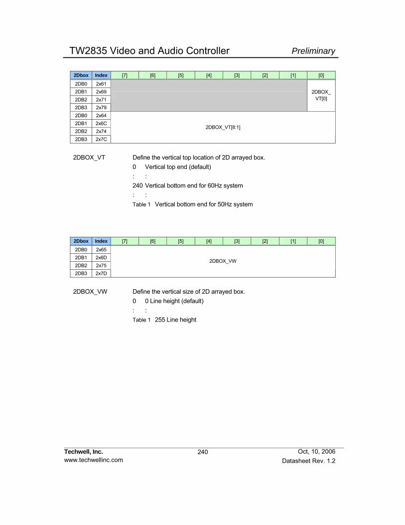
240
PreliminaryTW2835 Video and Audio Controller
Techwell, Inc. www.techwellinc.com Datasheet Rev. 1.2
Oct, 10, 2006
2Dbox Index [7] [6] [5] [4] [3] [2] [1] [0]
2DB0 2x61 2DB1 2x69 2DB2 2x71 2DB3 2x79
2DBOX_
VT[0]
2DB0 2x64 2DB1 2x6C 2DB2 2x74 2DB3 2x7C
2DBOX_VT[8:1]
2DBOX_VT Define the vertical top location of 2D arrayed box. 0 Vertical top end (default) : : 240 Vertical bottom end for 60Hz system : :
Table 1 Vertical bottom end for 50Hz system 2Dbox Index [7] [6] [5] [4] [3] [2] [1] [0]
2DB0 2x65 2DB1 2x6D 2DB2 2x75 2DB3 2x7D
2DBOX_VW
2DBOX_VW Define the vertical size of 2D arrayed box. 0 0 Line height (default) : :
Table 1 255 Line height

241
PreliminaryTW2835 Video and Audio Controller
Techwell, Inc. www.techwellinc.com Datasheet Rev. 1.2
Oct, 10, 2006
2Dbox Index [7] [6] [5] [4] [3] [2] [1] [0]
2DB0 2x66 2DB1 2x6E 2DB2 2x76 2DB3 2x7E
2DBOX_HNUM 2DBOX_VNUM
2DBOX_VNUM Define the row number of 2D arrayed box. For motion display mode, 11 is recommended. 0 1 Row : : 11 12 Row (default) : :
Table 1 16 Rows 2DBOX_HNUM Define the column number of 2D arrayed box. For motion display mode, 15 is recommended. 0 1 Column : :
Table 1 16 Columns (default) 2Dbox Index [7] [6] [5] [4] [3] [2] [1] [0]
2DB0 2x67 2DB1 2x6F 2DB2 2x77 2DB3 2x7F
2DBOX_CURHP 2DBOX_CURVP
2DBOX_CURHP Define the horizontal location of cursor cell within 2DBOX_HNUM. 0 1st Column (default) : :
Table 1 16th Column 2DBOX_CURVP Define the vertical location of cursor cell within 2DBOX_VNUM. 0 1st Row (default) : :
Table 1 16th Row

242
PreliminaryTW2835 Video and Audio Controller
Techwell, Inc. www.techwellinc.com Datasheet Rev. 1.2
Oct, 10, 2006
VIN Index [7] [6] [5] [4] [3] [2] [1] [0]
0 2x80 1 2xA0 2 2xC0 3 2xE0
MD_DIS MD
_REFFLD BD_CELSENS BD_LVSENS
0 2x81 1 2xA1 2 2xC1 3 2xE1
ND_LVSENS ND_TMPSENS
MD_DIS Disable the motion and blind detection. 0 Enable motion and blind detection (default) 1 Disable motion and blind detection MD_REFFLD Control the updating time of reference field for motion detection. 0 Update reference field every field (default) 1 Update reference field according to MD_SPEED BD_CELSENS Define the threshold of cell for blind detection. 0 Low threshold (More sensitive) (default) : : 3 High threshold (Less sensitive) BD_LVSENS Define the threshold of level for blind detection. 0 Low threshold (More sensitive) (default) : : 15 High threshold (Less sensitive) ND_LVSENS Define the threshold of level for night detection. 0 Low threshold (More sensitive) (default) : : 3 High threshold (Less sensitive) ND_TMPSENS Define the threshold of temporal sensitivity for night detection. 0 Low threshold (More sensitive) (default) : :
Table 1 High threshold (Less sensitive)
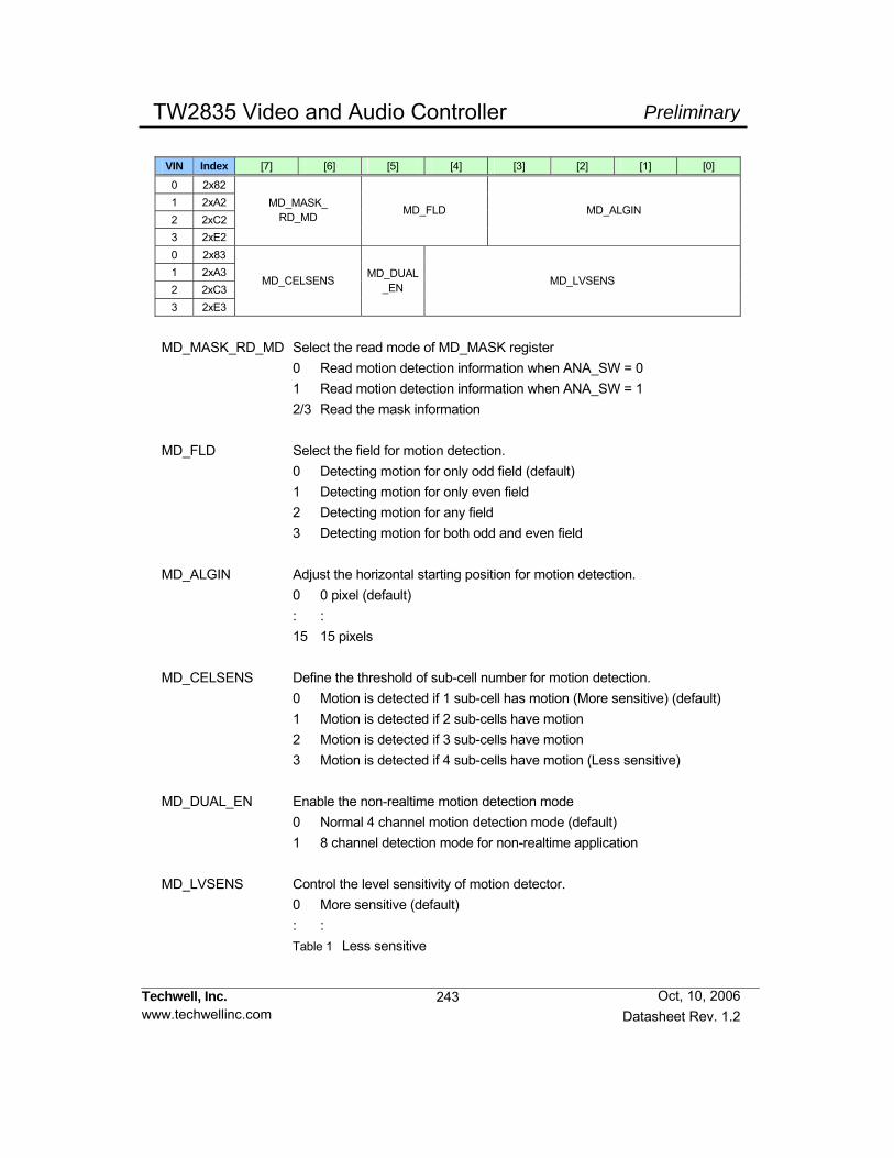
243
PreliminaryTW2835 Video and Audio Controller
Techwell, Inc. www.techwellinc.com Datasheet Rev. 1.2
Oct, 10, 2006
VIN Index [7] [6] [5] [4] [3] [2] [1] [0]
0 2x82 1 2xA2 2 2xC2 3 2xE2
MD_MASK_ RD_MD MD_FLD MD_ALGIN
0 2x83 1 2xA3 2 2xC3 3 2xE3
MD_CELSENS MD_DUAL
_EN MD_LVSENS
MD_MASK_RD_MD Select the read mode of MD_MASK register 0 Read motion detection information when ANA_SW = 0 1 Read motion detection information when ANA_SW = 1 2/3 Read the mask information MD_FLD Select the field for motion detection. 0 Detecting motion for only odd field (default) 1 Detecting motion for only even field 2 Detecting motion for any field 3 Detecting motion for both odd and even field MD_ALGIN Adjust the horizontal starting position for motion detection. 0 0 pixel (default) : : 15 15 pixels MD_CELSENS Define the threshold of sub-cell number for motion detection. 0 Motion is detected if 1 sub-cell has motion (More sensitive) (default) 1 Motion is detected if 2 sub-cells have motion 2 Motion is detected if 3 sub-cells have motion 3 Motion is detected if 4 sub-cells have motion (Less sensitive) MD_DUAL_EN Enable the non-realtime motion detection mode 0 Normal 4 channel motion detection mode (default) 1 8 channel detection mode for non-realtime application MD_LVSENS Control the level sensitivity of motion detector. 0 More sensitive (default) : :
Table 1 Less sensitive

244
PreliminaryTW2835 Video and Audio Controller
Techwell, Inc. www.techwellinc.com Datasheet Rev. 1.2
Oct, 10, 2006
VIN Index [7] [6] [5] [4] [3] [2] [1] [0]
0 2x84 1 2xA4 2 2xC4 3 2xE4
MD_ STRB_EN MD_STRB MD_SPEED
0 2x85 1 2xA5 2 2xC5 3 2xE5
MD_TMPSENS MD_SPSENS
MD_STRB_EN Select the trigger mode of motion detection 0 Automatic trigger mode of motion detection (default) 1 Manual trigger mode for motion detection MD_STRB Request to start motion detection on manual trigger mode 0 None Operation (default) 1 Request to start motion detection MD_SPEED Control the velocity of motion detector. Large value is suitable for slow motion detection. In MD_DUAL_EN = 1, MD_SPEED should be limited to 0 ~ 31. 0 1 field intervals (default) 1 2 field intervals : : 61 62 field intervals 62 63 field intervals 63 Not supported MD_TMPSENS Control the temporal sensitivity of motion detector. 0 More Sensitive (default) : : 15 Less Sensitive MD_SPSENS Control the spatial sensitivity of motion detector. 0 More Sensitive (default) : :
Table 1 Less Sensitive

245
PreliminaryTW2835 Video and Audio Controller
Techwell, Inc. www.techwellinc.com Datasheet Rev. 1.2
Oct, 10, 2006
Index Motion Detection Mask Control for VIN
Row VIN0 VIN1 VIN2 VIN3 [7] [6] [5] [4] [3] [2] [1] [0]
1 2x86 2xA6 2xC6 2xE6 2 2x88 2xA8 2xC8 2xE8 3 2x8A 2xAA 2xCA 2xEA 4 2x8C 2xAC 2xCC 2xEC 5 2x8E 2xAE 2xCE 2xEE 6 2x90 2xB0 2xD0 2xF0 7 2x92 2xB2 2xD2 2xF2 8 2x94 2xB4 2xD4 2xF4 9 2x96 2xB6 2xD6 2xF6 10 2x98 2xB8 2xD8 2xF8 11 2x9A 2xBA 2xDA 2xFA 12 2x9C 2xBC 2xDC 2xFC
MD_MASK[15:8]
1 2x87 2xA7 2xC7 2xE7 2 2x89 2xA9 2xC9 2xE9 3 2x8B 2xAB 2xCB 2xEB 4 2x8D 2xAD 2xCD 2xED 5 2x8F 2xAF 2xCF 2xEF 6 2x91 2xB1 2xD1 2xF1 7 2x93 2xB3 2xD3 2xF3 8 2x95 2xB5 2xD5 2xF5 9 2x97 2xB7 2xD7 2xF7 10 2x99 2xB9 2xD9 2xF9 11 2x9B 2xBB 2xDB 2xFB 12 2x9D 2xBD 2xDD 2xFD
MD_MASK[7:0]
MD_MASK Define the motion Mask/Detection cell for VIN MD_MASK[15] is right end and MD_MASK[0] is left end of column. In writing mode 0 Non-masking cell for motion detection (default) 1 Masking cell for motion detection In reading mode when MASK_MODE = “0” 0 Motion is not detected for cell 1 Motion is detected for cell In reading mode when MASK_MODE = “1” 0 Non-masked cell 1 Masked cell
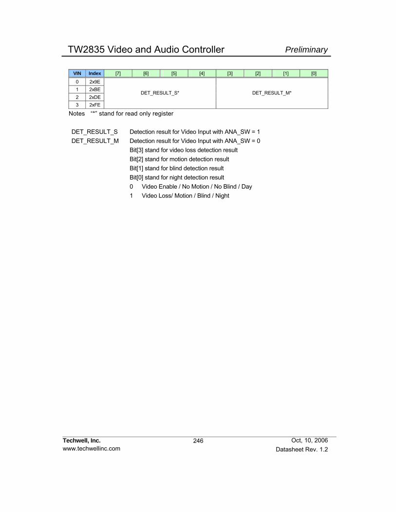
246
PreliminaryTW2835 Video and Audio Controller
Techwell, Inc. www.techwellinc.com Datasheet Rev. 1.2
Oct, 10, 2006
VIN Index [7] [6] [5] [4] [3] [2] [1] [0]
0 2x9E 1 2xBE 2 2xDE 3 2xFE
DET_RESULT_S* DET_RESULT_M*
Notes “*” stand for read only register DET_RESULT_S Detection result for Video Input with ANA_SW = 1 DET_RESULT_M Detection result for Video Input with ANA_SW = 0 Bit[3] stand for video loss detection result Bit[2] stand for motion detection result Bit[1] stand for blind detection result Bit[0] stand for night detection result 0 Video Enable / No Motion / No Blind / Day 1 Video Loss/ Motion / Blind / Night

247
PreliminaryTW2835 Video and Audio Controller
Techwell, Inc. www.techwellinc.com Datasheet Rev. 1.2
Oct, 10, 2006
Parametric Information
DC Electrical Parameters
Table 14 Absolute Maximum Ratings Parameter Symbol Min Typ Max Units
VDDADC (measured to VSSADC) VDDADCM -0.5 2.3 V VDDDAC (measured to VSSDAC) VDDDACM -0.5 2.3 V VDDI (measured to VSSI) VDDIM -0.5 2.3 V VDDO (measured to VSSO) VDDOM -0.5 4.5 V Voltage on Any Digital Data Pin (See the note below) - -0.5 4.5 V
Analog Input Voltage for ADC -0.5 2.0 V Storage Temperature TS -65 150 °C
Junction Temperature TJ 0 125 °C
Vapor Phase Soldering (15 Seconds) TVSOL 220 °C
NOTE: Long-term exposure to absolute maximum ratings may affect device reliability, and permanent damage may occur if operate exceeding the rating. The device should be operated under recommended operating condition.
Table 15 Recommended Operating Conditions Parameter Symbol Min Typ Max Units
VDDADC (measured to VSSADC) VDDADC 1.62 1.8 1.98 V VDDDAC (measured to VSSDAC) VDDDAC 1.62 1.8 1.98 V VDDI (measured to VSSI) VDDI 1.62 1.8 1.98 V VDDO (measured to VSSO) VDDO 3.0 3.3 3.6 V Analog VIN Amplitude Range (AC coupling required) VINR 0 0.5 1.0 V
Analog AIN Amplitude Range (AC coupling required) AINR 0 0.5 1.0 V
Ambient Operating Temperature TA -40 70 °C
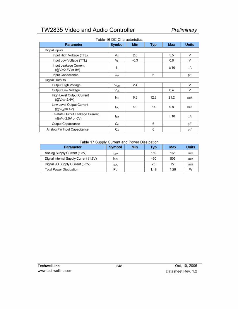
248
PreliminaryTW2835 Video and Audio Controller
Techwell, Inc. www.techwellinc.com Datasheet Rev. 1.2
Oct, 10, 2006
Table 16 DC Characteristics Parameter Symbol Min Typ Max Units
Digital Inputs Input High Voltage (TTL) VIH 2.0 5.5 V Input Low Voltage (TTL) VIL -0.3 0.8 V Input Leakage Current
(@VI=2.5V or 0V) IL ±10 µA
Input Capacitance CIN 6 pF Digital Outputs
Output High Voltage VOH 2.4 V
Output Low Voltage VOL 0.4 V
High Level Output Current (@VOH=2.4V) IOH 6.3 12.8 21.2 mA
Low Level Output Current (@VOL=0.4V) IOL 4.9 7.4 9.8 mA
Tri-state Output Leakage Current (@VO=2.5V or 0V)
IOZ ±10 µA
Output Capacitance CO 6 pF
Analog Pin Input Capacitance CA 6 pF
Table 17 Supply Current and Power Dissipation Parameter Symbol Min Typ Max Units
Analog Supply Current (1.8V) IDDA 150 165 mA
Digital Internal Supply Current (1.8V) IDDI 460 505 mA
Digital I/O Supply Current (3.3V) IDDO 25 27 mA Total Power Dissipation Pd 1.18 1.29 W

249
PreliminaryTW2835 Video and Audio Controller
Techwell, Inc. www.techwellinc.com Datasheet Rev. 1.2
Oct, 10, 2006
AC Electrical Parameters
Table 18 Clock Timing Parameters Parameter Symbol Min Typ Max Units
Delay from CLK54I to CLKVDO 1 4.7 12.5 ns Hold from CLKVDO (27MHz) to Data 2a 17 ns Delay from CLKVDO (27MHz) to Data 2b 21 ns Hold from CLK54I to Data 3a 8 ns Delay from CLK54I to Data 3b 12 ns Setup from PBIN to PBCLK 4a 5 ns Hold from PBCLK to PBIN 4b 5 ns Note : Cload = 25pF.
C LK54I
C LKVD O(27M H z)
Data Output
Data Output
3a3b
2b2a
1
C LKVD O(54M H z)
1
(A) 27MHz Output Mode
(B) 54MHz Output Mode
(C ) PBCLK Input T iming
PBCLK
PB_IN
4a 4b
C LK54I
Fig 80 Clock Timing Diagram
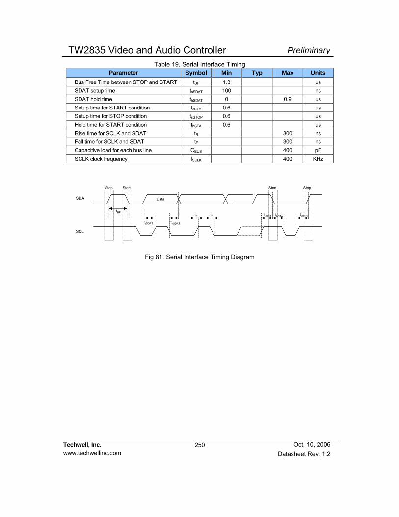
250
PreliminaryTW2835 Video and Audio Controller
Techwell, Inc. www.techwellinc.com Datasheet Rev. 1.2
Oct, 10, 2006
Table 19. Serial Interface Timing Parameter Symbol Min Typ Max Units
Bus Free Time between STOP and START tBF 1.3 us SDAT setup time tsSDAT 100 ns SDAT hold time thSDAT 0 0.9 us Setup time for START condition tsSTA 0.6 us Setup time for STOP condition tsSTOP 0.6 us Hold time for START condition thSTA 0.6 us Rise time for SCLK and SDAT tR 300 ns Fall time for SCLK and SDAT tF 300 ns Capacitive load for each bus line CBUS 400 pF SCLK clock frequency fSCLK 400 KHz
Stop Start
Data
StopStart
SDA
SCL
tBFthSTA tsSTOtsSTA
tsSDAT
tR tF
thSDAT
Fig 81. Serial Interface Timing Diagram

251
PreliminaryTW2835 Video and Audio Controller
Techwell, Inc. www.techwellinc.com Datasheet Rev. 1.2
Oct, 10, 2006
Table 20 Parallel Interface Timing Parameter Parameter Symbol Min Typ Max Units
CSB setup until AEN active Tsu(1) 10 ns
PDATA setup until AEN,WENB active Tsu(2) 10 ns
AEN, WENB, RENB active pulse width Tw 40 ns
CSB hold after WENB, RENB inactive Th(1) 60 ns
PDATA hold after AEN,WENB inactive Th(2) 20 ns
PDATA delay after RENB active Td(1) 12 ns
PDATA delay after RENB inactive Td(2) 60 ns
CSB inactive pulse width Tcs 60 ns RENB active delay after AEN inactive RENB active delay after RENB inactive Trd 60 ns
WriteIndex Address Write
CSB
WENB
RENB
AEN
PDATA
Tsu(1) Tcs
Th(2)Tsu(2)
Tw
Tw
Tsu(2)
Tw Th(1)
Th(2) Tsu(2) Th(2)
Fig 82 Write timing of parallel interface with auto index increment mode
ReadIndex Address Read
CSB
WENB
RENB
AEN
PDATA
Tsu(1) Tcs
Th(2)Tsu(2)
Tw
Tw
Td(1)
Tw Th(1)
Td(2)Td(2) Td(1)
Trd Trd
Fig 83 Read timing of parallel interface with auto index increment mode

252
PreliminaryTW2835 Video and Audio Controller
Techwell, Inc. www.techwellinc.com Datasheet Rev. 1.2
Oct, 10, 2006
Table 21.Analog Performance Parameter Parameter Symbol Min Typ Max Units
ADC characteristics Differential gain DGA 3 % Differential phase DpA 2 deg Channel Cross-talk αctA -50 dB
DAC characteristic Differential gain DGD 3 % Differential phase DpD 2 deg Channel Cross-talk αctA -50 dB
Table 22.Decoder Performance Parameter Parameter Symbol Min Typ Max Units
Horizontal PLL permissible static deviation ∆fH ±6 % Color Sub-carrier PLL lock in range ∆fSC ±800 Hz Video level tracking range AGC -6 18 dB Color level tracking range ACC -6 30 dB Oscillator Input
Nominal frequency fOSC 54 MHz Permissible frequency deviation ∆fOSC/fOSC ±100 ppm Duty cycle dtOSC 60 %
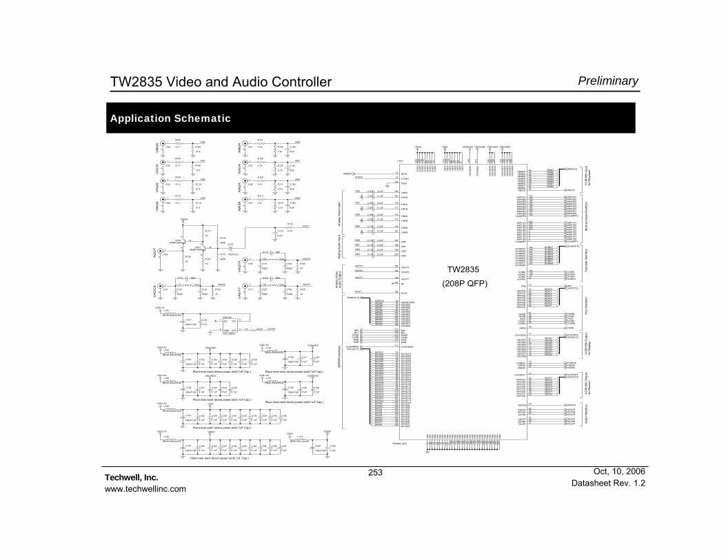
253
PreliminaryTW2835 Video and Audio Controller
Techwell, Inc. www.techwellinc.com Datasheet Rev. 1.2
Oct, 10, 2006
Application Schematic
VIN3
ADDR4
C142
0.1uF
ADDR2
VDOY6
+ C157
100uF/16V
R110
37.4
DATA15
C152
0.1uF
C113 2.2uF
MPP2[3]
AIN2
VAOCX
R100
37.4
Q100MMBT3904S
B
CE
R120
1KL100 1.8uH
Hos
t Int
erfa
ceADDR[10:0]
VDOY1
R121
1K
VA
OY
Y
PBIN2
VA
OY
X
HWRB
VDOY[7:0]
DLINKI2DLINKI1
C146
0.1uF
C107 0.1uF
VIN
0AA
OU
T
VDDI
VDOX4
VLINKI
DATA4
PBIN0
L106
BEAD 600ohm/2A
C121 18pF
DATA0
DATA11
C132
0.1uF
C101
15nF
J107
1
2
VDDI
RESETn
MPP2[0]
FLDENC
VDOY0
R12533
Cas
cade
Inte
rface
ASYNR
VDDAADC
DATA17
DATA28
C104 0.1uF
CLKVDOX
C109 0.1uF
HALE
DATA1
DATA9
C160
0.1uF
VDDVADC
PBIN5
L103
BEAD 600ohm/2A
R116
4.7K
HRDB
CLKVDOY
AOUT
+ C158
100uF/16V
C138
0.1uF
VDDO
DATA2
DLINKI5
C125
330pF
R119
200K
ADDR10
VDOY3
C151
0.1uF
Place near each device power pin(0.1uF Cap.)
ADDR0
VAOYX
DLINKI3
Place near each device power pin(0.1uF Cap.)
VDDO
VDD5A
DATA7
J100
1
2
C156
0.1uF
L102 1.8uH
MPP2[4]
C145
0.1uF
MPP2[2]
ACLKP
AOUT
CLK54I
DATA3
J110
1
2
L107
BEAD 600ohm/2A
VDD5A
VIN1
C114 2.2uF
C110 2.2uF MPP1[6]
J104
1
2
J109
1
2
WEBDQM
VAOCX
VDOY7
C141
0.1uF
VSENC
HDAT5
R112
37.4
C150
0.1uF
R114
37.4
Aud
io In
terfa
ce
C133
0.1uF
C148
0.1uF
IRQ
DATA10
C112
8.2nF
HDAT7
HLINKI
ADDR7
C119
330pF
AIN
1A
CLKMPP2
+ C147
100uF/16V
CLK54MEM
PBIN[7:0]
ADDR9
VDOX3
C102
15nF
VIN
1A
VDD3.3V
VDDADAC
VIN0
DATA29
CC
IR 6
56 In
put
for P
layb
ack
MPP2[5]
C111 0.1uF
+ C130
100uF/16V
VDD1.8V
HDAT[7:0]
ASYNP
DATA13
CASB
DATA31
ADDR3
MPP2[7]
DATA27
VDOX7
R108
37.4
DATA14
MPP1[5]
+ C127
100uF/16V
PBCLK
VDOY2
C164
0.1uF
C124
330pF
+ C129
100uF/16V
R101
4.7K
Place near each device power pin(0.1uF Cap.)
VDD1.8V
ADATM
DATA26
C161
0.1uF
R103
4.7k
R109
4.7k
R122
75
Ana
log
Vid
eo In
put
RASB
R106
37.4
C103 2.2uF
Place near each device power pin(0.1uF Cap.)
VIN2
VIN1
HDAT3
C123
330pF
AIN
0A
ADDR5
C137
0.1uF
J102
12
R102
37.4
Place near each device power pin(0.1uF Cap.)
DATA18
DLINKI4
VDOX6
C168
0.1uF
HDAT0
L104
BEAD 600ohm/2A
C159
0.1uF
SD
RA
M In
terfa
ce
MPP1[0]
VIN0
VAOYX
AIN1
OSC100
OSC 54MHz
1
4 5
8NC
GND OUT
VCC
BA1
MPP2[1]
R115
4.7k
J103
1
2
C143
0.1uF
L109
BEAD 600ohm/2A
VDDADAC
HCSB1
ADATP
DATA12
HDAT2
R124
75
MPP1[4]
ADDR8
DATA19
+
C115
10uF/6.3V
L110
BEAD 600 ohm/2A
DATA30
HDAT1
AIN
2A
VDD3.3V
VDD5
AIN3
VDOX5
C163
0.1uF
C149
0.1uF
C117 18pFDLINKI6
VDDVDAC
MPP1[2]
ACLKR
R111
4.7k
C108 2.2uF
C136
0.1uF
MPP1[7]
DATA5
ADDR1
PBIN4
VDOX0
DATA22
PBIN3
C166
0.1uF
C167
0.1uF
C106
15nF
VDD1.8V
ALINKI
CLK54I
DLINKI0
Q101MMBT3904S
B
CE
J106
1
2
+ C139
100uF/16V
C105 2.2uF
Mul
ti-pu
rpos
e In
terfa
ce
C144
0.1uF
DATA6
C100
15nF
DATA24
AIN1
VAOYY
ALINKO
VDOY4
J101
1
2
VIN
2A
VDDAADC
VIN3
AIN
3A
Place near each device power pin(0.1uF Cap.)
HSPB
DLINKI7
R123
75
C116 2.2uF
C131
0.1uF
ADDR6
DATA16
PBIN6
VIN
3A
VDOY5
HCSB0
C126
330pF
VDOX[7:0]
VA
OC
X
HSENC
C162
0.1uF
C135
0.1uF
R118
400K
L108
BEAD 600ohm/2A
MPP2[6]
DLINKI[7:0]
AIN0
C154
0.1uF
R117
2K
C128
0.1uF
L105
BEAD 600ohm/2A
AIN2
C118 2.2uF
+ C140
100uF/16V
Ana
log
Aud
io In
put
BA0
VIN2
J111
1
2
MPP1[3]
DATA20
CLKMPP1
ADATR
DATA8
DATA21
VDOX1
R105
4.7K
C122 18pF
R104
37.4
CC
IR 6
56 O
utpu
tfo
r Rec
ord
DATA[31:0]
MPP1[1]
DATA23
VDOX2
C165
0.1uF
C134
0.1uF
TW2835
(208P QFP)
U100
TW2835_QFP
208
157
139
110
93 64 47 18 151
133
116
99 58 41 24 6 193
201
190
187
185
182
175
173
172
165
1 12 29 35 52 53 70 75 81 87 104
105
122
128
145
156
162
163
168
169
174
178
179
183
188
192
195
196
202
203
434445464849505154
152153154155158159160161150
20420520620723457
149148147146144143142141
14013813722
72
7169686766656362
6160595756
55
17
89101113141516
192021
32
3334363738394042
23
252627
283031
73
74
164
166
167
170
171
176
177
180
181
197
198
199
200
184
186
189
191
194
95969798
100101102103106107108
111109113114115117
112
76777879808283848586888990919294
118119120121123124125126127129130131132134135136
VD
DO
VD
DO
VD
DO
VD
DO
VD
DO
VD
DO
VD
DO
VD
DO
VD
DI
VD
DI
VD
DI
VD
DI
VD
DI
VD
DI
VD
DI
VD
DI
VD
DA
DA
C
VD
DA
AD
C
VD
DV
DA
CV
DD
VD
AC
VD
DV
DA
C
VD
DV
AD
CV
DD
VA
DC
VD
DV
AD
CV
DD
VA
DC
VD
DV
AD
C
VS
SV
SS
VS
SV
SS
VS
SV
SS
VS
SV
SS
VS
SV
SS
VS
SV
SS
VS
SV
SS
VS
SV
SS
VS
SV
SS
VS
SV
SS
VS
SV
SS
VS
SV
SS
VS
SV
SS
VS
SV
SS
VS
SV
SS
PBIN[7]PBIN[6]PBIN[5]PBIN[4]PBIN[3]PBIN[2]PBIN[1]PBIN[0]PBCLK
MPP2[7]MPP2[6]MPP2[5]MPP2[4]MPP2[3]MPP2[2]MPP2[1]MPP2[0]
CLKMPP2
MPP1[7]MPP1[6]MPP1[5]MPP1[4]MPP1[3]MPP1[2]MPP1[1]MPP1[0]
CLKMPP1
DLINKI[7]DLINKI[6]DLINKI[5]DLINKI[4]DLINKI[3]DLINKI[2]DLINKI[1]DLINKI[0]
VLINKIHLINKIALINKI
ALINKO
IRQ
HDAT[0]HDAT[1]HDAT[2]HDAT[3]HDAT[4]HDAT[5]HDAT[6]HDAT[7]
HWRBHRDBHALE
HCSB1HCSB0
HSPB
CLKVDOX
VDOX[7]VDOX[6]VDOX[5]VDOX[4]VDOX[3]VDOX[2]VDOX[1]VDOX[0]
FLDENCVSENCHSENC
CLKVDOY
VDOY[7]VDOY[6]VDOY[5]VDOY[4]VDOY[3]VDOY[2]VDOY[1]VDOY[0]
ADATM
ADATRASYNRACLKR
ADATPASYNPACLKP
RSTB
CLK54I
TEST
VIN0A
VIN0B
VIN1A
VIN1B
VIN2A
VIN2B
VIN3A
VIN3B
AIN0
AIN1
AIN2
AIN3
VAOYX
VAOCX
VAOYY
NC
AOUT
ADDR[10]/APADDR[9]ADDR[8]ADDR[7]ADDR[6]ADDR[5]ADDR[4]ADDR[3]ADDR[2]ADDR[1]ADDR[0]
BA0BA1RASBCASBWEBDQM
CLK54MEM
DATA[31]DATA[30]DATA[29]DATA[28]DATA[27]DATA[26]DATA[25]DATA[24]DATA[23]DATA[22]DATA[21]DATA[20]DATA[19]DATA[18]DATA[17]DATA[16]DATA[15]DATA[14]DATA[13]DATA[12]DATA[11]DATA[10]DATA[9]DATA[8]DATA[7]DATA[6]DATA[5]DATA[4]DATA[3]DATA[2]DATA[1]DATA[0]
C155
0.1uF
DATA25
PBIN7
C153
0.1uF
VDD1.8V
R113
4.7k
VDDVDAC
HDAT6
VDD1.8V
HDAT4
AIN0
J105
1
2
CC
IR 6
56 O
utpu
tfo
r Dis
play
AIN3J108
1
2
VDDVADC
VAOYY
R107
4.7k
C120
330pF
Ana
log
Vid
eoA
udio
Out
put
PBIN1
L101 1.8uH

254
PreliminaryTW2835 Video and Audio Controller
Techwell, Inc. www.techwellinc.com Datasheet Rev. 1.2
Oct, 10, 2006
Package Dimension
208 QFP
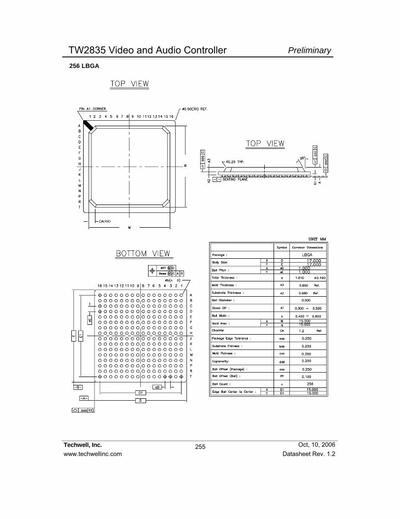
255
PreliminaryTW2835 Video and Audio Controller
Techwell, Inc. www.techwellinc.com Datasheet Rev. 1.2
Oct, 10, 2006
256 LBGA

256
PreliminaryTW2835 Video and Audio Controller
Techwell, Inc. www.techwellinc.com Datasheet Rev. 1.2
Oct, 10, 2006
Revision History
Table 23 Datasheet Revision History
Revision Date Description Product Code
1.0 Jul. 05. 2006 Preliminary Datasheet Release BAPA1
1.1 Jul. 10.2006
Update the Errata 1) Update the Fig 49 ~ Fig 52 for SYNC_DEL value (P. 78 ~ P. 81) Update the register description for SYNC_DEL (P. 208) 2) Update the register description for VIS_CODE_EN (P.209) 3) Update the register description for 2DBOX_HL (P.239)
BAPA1
1.2 Oct. 10. 2006
Update the Errata 1) Update the description of noise reduction (P. 69) 2) Update the Fig 52 (P. 81) 3) Correct the register address mismatch (P.83, P.87, P.88) 4) Update the register description for NR_EN (P. 116) 5) Update the register description for MIX_OUTSEL (P.155) 6) Remove the register description for ENHANCE (P. 198) 7) Update the recommended schematic for Audio LPF filter (P.253)
BAPA1