4-1 FINAL for Tom Dillinger
39
<Insert Picture Here> Challenges for FinFET Extraction Tom Dillinger IEEE Electronic Design Process Symposium, 4/19/2013
-
Upload
ashishj1083 -
Category
Documents
-
view
31 -
download
1
Transcript of 4-1 FINAL for Tom Dillinger

<Insert Picture Here>
Challenges for FinFET Extraction Tom Dillinger IEEE Electronic Design Process Symposium, 4/19/2013

2
Outline
1) FinFET transistor overview
• cross-sections • electrical behavior • dummy gates for process uniformity
2) Parasitic FinFET elements • gate input capacitance • gate input equivalent resistance • source/drain “spreading” resistance
3) Challenges for the FinFET extracted parasitic model 4) Summary

3
FinFET transistor overview

4
What is a FinFET?
Fins can be made on SOI material, or on bulk silicon.
Lots of technical research on 3D FET channel topologies... The most promising option is to create a vertical silicon “fin” for the device channel.
“Benchmarking SOI and bulk FinFET alternatives for PLANAR CMOS scaling succession”, Solid-State Electronics, Volume 54, Issue 9, Sept. 2010, p. 855-860.

5
Intel's FinFET technology on IvyBridge
Recent transmission electronic microscopy photos of Intel's Ivy Bridge (bulk) FinFET's illustrate a more “rounded” profile. This profile is easier to fabricate – yet, it also has a strong impact on the transistor (and extraction) characteristics.
http://www.chipworks.com/blog/technologyblog/2012/04/intel%E2%80%99s-22-nm-tri-gate-transistors-exposed/

6
What is a FinFET? “Sidewall Image Transfer”
A silicon “fin” is made through highly anisotropic etching of a silicon layer, typically defined by a spacer deposited over a sacrificial patterned layer:
(SOI cross-section shown above. The spacer process is referred to as “Sidewall Image Transfer”, or SIT.)
Wade Xiong, “FinFET’s and Other Multi-Gate Transistors”, J.P. Colinge (Ed.), Springer, 2008.

7
What is a FinFET? Process variation
Sources of variation in the fin geometry include: • Fin height (higher variation in bulkSi) • Fin thickness • Fin corner rounding profile • Fin sidewall roughness • Gate line edge roughness (LER) • Gate CD length variation over multiple, parallel fins
Baravelli, et al, “Impact of Line Edge Roughness and Random Dopant Fluctuation on FinFET Matching Performance”, IEEE Transactions on Nanotechnology, v.7(3), May 2008.
NOTE: There are additional sources of process variation that define the device threshold voltage, in addition to the fin geometry.

8
What is a FinFET? “tri-gate” or “dual-gate” device
Two fabrication options – a “dual-gate” or a “tri-gate” FinFET. Dual-gate FinFET • A “hard mask” dielectric is retained on top of the fin. • The electric field from the gate to the fin on the top is drastically reduced.
Lin, et al, "Channel Doping Impact on FinFET's for 22nm", VLSI Symposium 2012

9
What is a FinFET? “tri-gate” or “dual-gate” device
Tri-gate FinFET • The tri-gate adds the top fin surface to active device channel. • The tri-gate will exhibit some “soft” Vt channel inversion at the corners.
Id vs. radius of curvature of fin corner, from: Doyle, et al., “Tri-Gate Fully Depleted CMOS Transistors”, VLSI Technology Symposium, 2003.

10
What is a FinFET? a “fully-depleted (volume) channel”
• The finFET channel is typically “fully depleted” by the gate voltage in the off state → little body effect (Vt dependency upon substrate bias).

11
What is a FinFET? reducing Rs and Rd through SEG
• Additional processing steps are taken to reduce the resistance of the source/drain regions (Rs, Rd).
• Selective Epitaxial Growth adds silicon volume, after the FinFET gate is formed – a “raised” source/drain.
• gate spacer defines SEG volume • reduces Rs_total and Rd_total: (Roverlap + Rext + Rspreading) • different SEG for nFET's & pFET's (SiGe for pFET's for mobility enh.) • higher Cgs and Cgd
Wade Xiong, “FinFET’s and Other Multi-Gate Transistors”, J.P. Colinge (Ed.), Springer, 2008.

12
What is a FinFET? reducing Rs and Rd through SEG
• Selective Epitaxial Growth (SEG) results in source/drain regions that are dependent upon the starting sidewall crystal surface orientation.
poly gate: green fins: pink source/drain extensions: purple M0 local interconnect: blue
Kelin Kuhn, “22nm Device Architecture and Performance Elements”, IEDM 2008.

13 © 2012 Oracle Corporation – Proprietary and Confidential
What is a FinFET? Rs/Rd, from fin to raised epi
Source/drain current density in SEG fin cross-section
with top silicide, (100) and (110) surface examples. From: Kawasaki, et al, IEDM 2009, p. 289-292.

14
BSIM-CMG models
• There is a specific BSIM compact model for multi-gate FET's released by the UC-Berkeley modeling team: http://www-device.eecs.berkeley.edu/bsim/ http://www.eecs.berkeley.edu/Research/Projects/Data/101953.html [1] D. D. Lu, C.-H. Lin, S. Yao, W. Xiong, F. Bauer, C. R. Cleavelin, A. M. Niknejad and C. Hu, " Design of FinFET SRAM Cells using a Statistical Compact Model," Simulation of Semiconductor Processes and Devices (SISPAD), pp. 127-130, Sept. 2009.
• Other researchers are also proposing FinFET compact models.
• The Compact Model Council is an industry-wide collaboration, to “standardize” simulation models. • The CMC recently standardized on the BSIM-CMG model, so that SPICE simulation tool developers could develop model support.

15
BSIM-CMG models – Ids device current
• The BSIM-CMG device current and model utilizes the multiplicative factor “NFIN_total”, the product of the ((# of fins per finger) * (# of fingers)):
(The expectation is that local fin variations would be “averaged” into a single instance of the device model.)

16
BSIM-CMG models – Rs and Rd
• The BSIM-CMG source/drain resistance model offers multiple options:
• simple “sheet resistance” method (sheet rho * # of squares)
• a complex “spreading resistance” model through the raised S/D epi
17
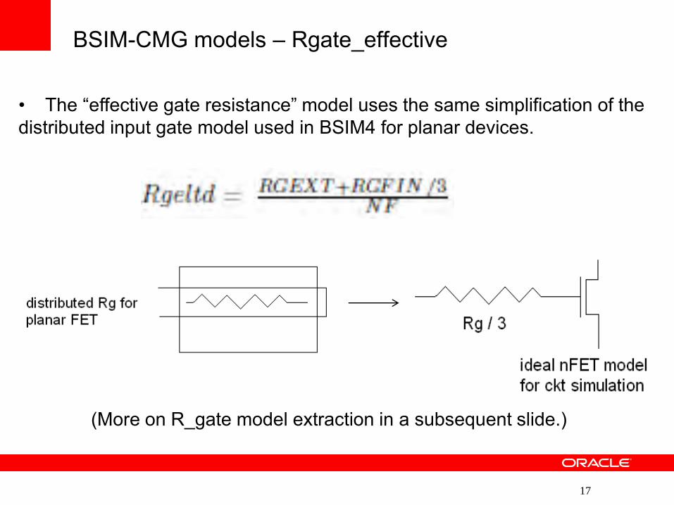
BSIM-CMG models – Rgate_effective
• The “effective gate resistance” model uses the same simplification of the distributed input gate model used in BSIM4 for planar devices.
(More on R_gate model extraction in a subsequent slide.)

18
BSIM-CMG models – Layout Dependent Effects
• The BSIM-CMG models do not currently include “Layout Dependent Effect” parameters (not to the extent present in BSIM4):
Example: LOD effect: dependent upon the distance from gate channel to active edge derived from crystal stress from STI and stress liners

19
Dummy devices for process uniformity
• The ends of the fins include a “dummy” gate, which is also part of the parasitic FinFET model:
http://chipdesignmag.com/sld/blog/2011/05/26/

20
Dummy devices for process uniformity
• The ends of the fins include a “dummy” gate, which is also part of the parasitic FinFET model (cross-sectional view):
http://www.chip-architect.com/news/2012_04_19_Ivy_Bridges_GPU_2-25_times_Sandys.html

21
Parallel FinFET devices for drive current
“Intel will use up to six fins, traversed by a single gate, in circuits requiring high drive current.” http://semiimd.com/blog/2011/05/16/intel-tri-gate-advantages-“worth-the-effort”

22
Parasitic FinFET elements

23
Parasitic FinFET extraction – Cgs, Cgd, and Cgx
• In addition to the intrinsic device capacitances, there are external parasitic capacitances – Cgs and Cgd (both sidewall and top), and Cgx • These capacitances are distributed between (parallel) fins, a topology not present in planar structures.
FinFET gate-to-S/D sidewall cap.

24 © 2012 Oracle Corporation – Proprietary and Confidential
Parasitic FinFET extraction – Cgs, Cgd (sidewall)
Cgs/Cgd – another sidewall view

25 © 2012 Oracle Corporation – Proprietary and Confidential
Parasitic FinFET extraction – Cgs, Cgd (top)
Cgs/Cgd, top of fin 20nm had raised S/D, as well, but not faceted fins

26
Parasitic FinFET extraction – Cgx
• The gate-to-substrate capacitance, Cgx, differs from a planar structure, with additional Cgx between parallel fins.

27
Parasitic FinFET extraction – Rgate_equivalent
• There is also the question of what model is needed for the equivalent gate input resistance, Rgate.

28
Parasitic FinFET extraction – ITF
ITF format to support FinFET's MULTIGATE fin1 { FIN_SPACING = <space of fin> FIN_WIDTH = <width of fin> FIN_LENGTH = <length of fin> FIN_THICKNESS = <thickness of fin> GATE_OXIDE_TOP_T=<gate oxide top thickness> GATE_OXIDE_SIDE_T=<gate oxide side thickness> (optional) GATE_OXIDE_ER=<gate oxide permittivity> GATE_POLY_TOP_T=<poly top thickness> GATE_POLY_SIDE_T=<poly side thickness> (optional) CHANNEL_ER = <CHANNEL ER> GATE_DIFFUSION_LAYER_PAIR {(PGATE PDIFF)(NGATE NDIFF)} }
Note that this enhanced ITF format assumes an ideal rectangular fin profile.

29
Parasitic FinFET extraction – S/D coupling to dummy gate
• There is also a local parasitic capacitance from FinFET S/D to the dummy gate.
NOTE: Local metal “M0” on S/D not shown, but that also contributes significantly to the capacitive coupling geometry. .

30
Challenges for the parasitic FinFET model

31
Parasitic reduction
• To annotate the extracted model, it is necessary to “reduce” the parasitic elements to the corresponding device netlist.
• Individual FinFET extracted capacitances (Cgs, Cgd, Cgx, Csx, Cdx), resistances (Rs and Rd), and “Rgate” need to be suitably reduced to annotate to the netlist model derived from schematics.

32
FinFET Extraction with variation sensitivity
• Recent enhancements to parasitic extraction SPEF format include support for process variation:
IEEE Std 1481-2009 http://ieeexplore.ieee.org/stamp/stamp.jsp?tp=&arnumber=5430852
• To date, there hasn’t been substantial development to represent
the SPEF *VARIATION_PARAMETERS for FinFET extraction.

33
Summary

34
Summary
• FinFET topologies are substantially different than planar. • The actual profile of the fin may be quite different from the
“ideal” rectangular cross-section. (Approximations for parasitic extraction will be required.)
• The BSIM-CMG model currently represents some, but not all, of the device characteristics (compared to BSIM4):
• Layout Dependent Effects • Rgate_equivalent

35
Summary
• It is crucial to review the parasitic reduction methodology with your EDA vendor, for suitable accuracy and dataset size:
• Needs to support general netlist annotation methodology • reduction of distributed RC parasitics across parallel fins and
fingers required • Needs to support calculation of Rgate, with suitable accuracy
• correlates to the number of parallel fins used • Needs to reflect dummy FinFET gate parasitics
• The utilization of *VARIATION_PARAMETERS for FinFET extraction is still to be explored.

36
BACKUP SLIDES

37
What is a FinFET? “volume” device current
For narrow fins, volume inversion will occur. Carrier mobility is higher, due to less surface scattering. Improvements of 20% in device current due to “volume” carriers have been reported, compared to two separate surface channel currents.

38
What is a FinFET? “quantum density of free carrier states”
For very narrow fins, the improvements in device current due to improved mobility and volume inversion is mitigated by the “quantum” density of free carrier states. A “correction” in the device current models is typically applied for narrow fins, due to the quantum DoS.
39
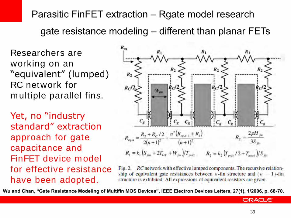
Parasitic FinFET extraction – Rgate model research
Researchers are working on an “equivalent” (lumped) RC network for multiple parallel fins.
Yet, no “industry standard” extraction approach for gate capacitance and FinFET device model for effective resistance have been adopted.
gate resistance modeling – different than planar FETs
Wu and Chan, “Gate Resistance Modeling of Multifin MOS Devices”, IEEE Electron Devices Letters, 27(1), 1/2006, p. 68-70.