38328 CH04 Meyer - Computer Science€¦ · · 2012-07-31The other box has only 1 or 0 in it....
16
Objectives ■ Experiment with digital logic circuits using a simple logic gate simulator. References Software needed: 1) A web browser (Internet Explorer or Netscape) 2) Applet from the lab website: a) LogicGates applet Textbook reference: Chapter 4, pp. 96–112. Logic Circuits 4 Laboratory Laboratory
Transcript of 38328 CH04 Meyer - Computer Science€¦ · · 2012-07-31The other box has only 1 or 0 in it....

Objectives■ Experiment with digital logic circuits using a simple logic gate simulator.
ReferencesSoftware needed:
1) A web browser (Internet Explorer or Netscape)
2) Applet from the lab website:
a) LogicGates applet
Textbook reference: Chapter 4, pp. 96–112.
Logic Circuits 4LaboratoryLaboratory
38328_CH04_Meyer.qxd 11/8/05 2:52 PM Page 51

BackgroundEverything you need to learn is explained in Chapter 4, “Gates and Circuits.”
ActivityDigital logic circuits are the bedrock of computer design. CPU chips such as the IntelPentium or AMD Athlon are silicon wafers in which millions of circuits are embedded.Everything your computer does depends upon them.
In this lab, we will learn how to use the “LogicGates” applet to draw and testdigital logic circuits. Chip manufacturers, such as Intel and AMD, use sophisticated(and extremely expensive) software to help them design and test their chips. But thebasic idea is the same.
First, start the “LogicGates” applet. You can load a number of examples by pullingdown the example choice pull-down menu. Load Example 1 “simple,” as shown here:
Each logic gate has a distinctive shape (see pp. 96–100). The wire coming out ofthe gate shows its current value. Gates are oriented so that their inputs come in fromthe left side and their outputs go out from the right side. This cannot be changed norcan the gates be rotated in this applet.
Two special boxes exist for input and output. The switch box has a lever in italong with 1 or 0. To flip the lever and change the value, click on the number right inthe center. The other box has only 1 or 0 in it. This is the output box that accepts awire from a gate and displays its value.
To propagate new values through the circuit, click on the Run button. It changesto say Stop so that when you click on it again, the simulator stops running. When thecircuit is running, you can click on the switches and watch values change throughoutthe circuit.
52 | Laboratory 4
38328_CH04_Meyer.qxd 11/8/05 2:52 PM Page 52

To practice using the simulator, we’ll build the logic circuit shown on p. 105 of thetextbook. First, if your simple example circuit is still running, press the Stop button.Now, clear the screen by clicking on the Clear button. To build the circuit, you’ll needthree switches, two AND gates, one OR gate, and one output box. To create them, clickon the New button, pull down the gate menu and select the gate or other item youwant. Then click once where you want the switch, gate, or output box to sit. You canreposition gates, switches, and outputs by dragging them to a new location.
Notice that when you are adding gates, the New button changes to say *New. Most ofthe buttons in this applet work like this: they show they are still active by displaying anasterisk in front of the label on the button. Because the button stays active, you can clickon different gates without having to re-click the New button over and over.
Click on the New button again to stop adding components. The asterisk will goaway.
Let’s also attach labels to the boxes to mimic the circuit diagram on p. 105.However, in the Logic Gate simulator, labels attach to boxes, not wires as they do inthe textbook.
First click on the Label button, which allows us to label gates and switches. Thenclick on the top switch. A textfield opens up right above the switch. Type “A” into itand press Return.
Here’s what you should see:
Logic Circuits | 53
38328_CH04_Meyer.qxd 11/8/05 2:52 PM Page 53

Label the middle switch as B and the bottom switch as C. Also label the output X.If you want to be complete, label the top AND gate as D and the bottom AND gate asE. When done labeling, click on the Label button so that the asterisk doesn’t appear.
Now it’s time to connect the gates, so click on the Connect button. Click once onswitch “A.” A red line flashes into view, anchored in the center of the switch andfollowing the mouse pointer around the screen. Click on the top AND gate. Repeat thisprocess and connect all the boxes so they match the screenshot below. If you make amistake, click on the Disconnect button, then click on a gate. All lines between thatgate and all other components will be removed.
A gate’s output may have any number of wires coming out of it so that it connectsto more than one other gate. Merely select the same gate as the left end of a wire morethan once.
Automatic elbows break lines up into horizontal and vertical segments. To see aversion that uses diagonal lines, click on the Stepped button. However, in most circuitfabrication technologies, all wires must lie on a grid so diagonal wires are eitherimpossible or expensive. To see the elbowed lines again, click on the bottom button,which has changed from Stepped to Diagonal.
Sometimes the elbows make it hard to see overlapped wires, and that plagues thiscircuit. So move the bottom AND gate a little to the left until the wires show moreclearly.
Here’s the final picture:
Now run the circuit by clicking the Run button. Click on the switches to changetheir values. Record the results in a truth table and see if the circuit gives you the sameresults as shown on p. 106 of your textbook. They had better agree! (They will, don’tworry.)
Imagine what a terrible thing it would be if a major chip manufacturer’ssimulation software didn’t give the right values and they sent a chip into productionwith flaws in it. Well, actually, don’t bother imagining: It’s already happened! In theearly 1990s, Intel recalled their new Pentium processor when scientists and engineers
54 | Laboratory 4
38328_CH04_Meyer.qxd 11/8/05 2:52 PM Page 54

pointed out that in certain calculations the chip gave the wrong answer! Analysts haveestimated that this bug in the chip’s division algorithm cost the company about $500million. (Too bad they weren’t using our simulator to check their circuit design!)
Our simulator provides you with six types of gates: AND, OR, NOT, NAND, NOR,and XOR. All of these are defined in Chapter 4 of the textbook. Another type of “gate”available in our circuit simulation is the Truth table, which allows you to avoidbuilding really complicated circuits with lots of gates. Instead, you fill in the truthtable values and the simulator treats it as a gate. A truth table “gate” can have two,three, or more inputs.
Let’s build a circuit using truth tables. Clear the screen and add three new switchesand one output.
The trickiest part is putting the right size truth table into the circuit. To do this,make sure the New button is activated (has an asterisk next to *New.) Then pull downon the gates menu and bring Truthtable into view. In the yellow message box, LogicGates will ask you how many inputs your truth table should have. The default is 2, butsince we have 3 switches, replace the 2 with 3. Then click once in the middle of thearea to create the truth table. Click off the New button and connect these gates asshown below:
Important note! Make sure that when you connect the switches, you connect thetop one first, then the middle one, and finally the bottom one. This is necessarybecause the order of the incoming wires determines which value is associated withwhich column in the truth table. The first wire connected will correspond to the firstcolumn in the table, the second wire will correspond to the second column, and so on.If you connect them in a different order, the wires going into the truth table will notcorrespond to the columns of your truth table.
New truth tables list all the input values in canonical order, but since the output isshown as always 0, we need to edit the truth table so it implements our desired output.To edit a truth table, click once on it (after making sure that all the buttons on the leftare off, i.e., do not have asterisks in front of their names). This makes the truth table
Logic Circuits | 55
38328_CH04_Meyer.qxd 11/8/05 2:52 PM Page 55
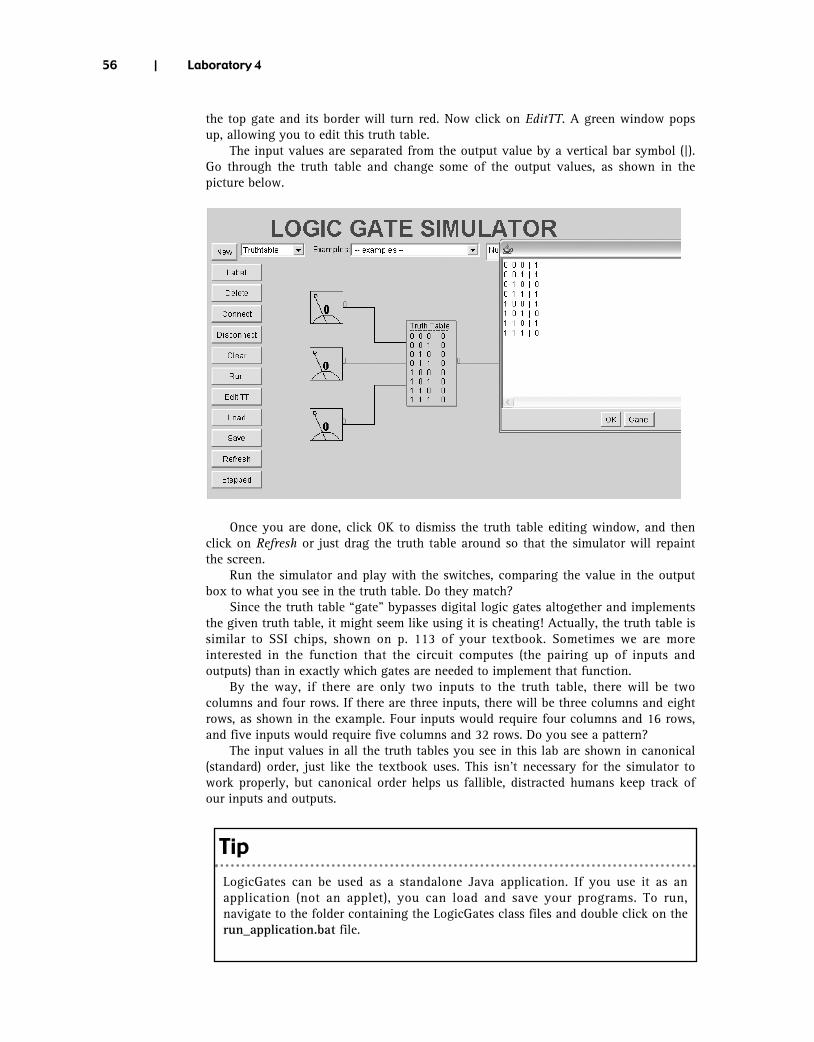
the top gate and its border will turn red. Now click on EditTT. A green window popsup, allowing you to edit this truth table.
The input values are separated from the output value by a vertical bar symbol (|).Go through the truth table and change some of the output values, as shown in thepicture below.
Once you are done, click OK to dismiss the truth table editing window, and thenclick on Refresh or just drag the truth table around so that the simulator will repaintthe screen.
Run the simulator and play with the switches, comparing the value in the outputbox to what you see in the truth table. Do they match?
Since the truth table “gate” bypasses digital logic gates altogether and implementsthe given truth table, it might seem like using it is cheating! Actually, the truth table issimilar to SSI chips, shown on p. 113 of your textbook. Sometimes we are moreinterested in the function that the circuit computes (the pairing up of inputs andoutputs) than in exactly which gates are needed to implement that function.
By the way, if there are only two inputs to the truth table, there will be twocolumns and four rows. If there are three inputs, there will be three columns and eightrows, as shown in the example. Four inputs would require four columns and 16 rows,and five inputs would require five columns and 32 rows. Do you see a pattern?
The input values in all the truth tables you see in this lab are shown in canonical(standard) order, just like the textbook uses. This isn’t necessary for the simulator towork properly, but canonical order helps us fallible, distracted humans keep track ofour inputs and outputs.
56 | Laboratory 4
TipLogicGates can be used as a standalone Java application. If you use it as anapplication (not an applet), you can load and save your programs. To run,navigate to the folder containing the LogicGates class files and double click on therun_application.bat file.
38328_CH04_Meyer.qxd 11/8/05 2:52 PM Page 56

Exercise 1
Logic Circuits | 57
Name __________________________________________ Date _______________________
Section _________________________________________
1) Start the “LogicGates” applet.
2) Add two switches, one XOR and one output, and connect them.
3) Press the Run button and try out all four combinations of inputs for the switches, recording theresults in a truth table. Take screenshots for each combination.
38328_CH04_Meyer.qxd 11/8/05 2:52 PM Page 57

Exercise 2
58 | Laboratory 2
Name __________________________________________ Date _______________________
Section _________________________________________
1) Start the “LogicGates” applet.
2) Create the same circuit as previously, but this time insert a NOT box between XOR and the output.
3) Press the Run button and try out all four values by changing the switch values. You do not have totake screenshots, but again record the results in a truth table so you can see the values.
4) What does this circuit do? Study your truth table to determine its function. (Hint: It yields a trueresult only when inputs A and B share a particular relationship. What is that relationship?)
38328_CH04_Meyer.qxd 11/8/05 2:52 PM Page 58

Exercise 3
Logic Circuits | 59
Name __________________________________________ Date _______________________
Section _________________________________________
1) Start the “LogicGates” applet.
2) Build a new circuit that will be a larger version of the one you created in Exercise 2. There will befour switches. Assign them the labels A1, A0, B1, and B0. (Note: A1 is a way of specifying A1when you can’t really have a subscript.)
3) The circuit will have two XORs, two NOTs, an output, and a mystery box, arranged as shownbelow:
4) The purpose of this circuit is to compare two 2-bit binary numbers to see if they are the samenumber. For example, suppose A (that is, the two-digit number comprised of A1A0) is 10 and B (thetwo-digit number B1B0) is 10, then the output box will display 1. If A is 10 but B is 11, the outputbox will show 0, which is Boolean-ese for “false.”
5) Connect the XOR boxes to the proper input switches. (Just think about how you compare twonumbers for equality. What digits do you compare?)
6) The “mystery gate” is either AND or OR. You can either experiment until you get the right answer,or, better for your brain (and more impressive to your teacher) you can reason out which it shouldbe.
7) Take a screenshot showing your circuit getting the correct result.
38328_CH04_Meyer.qxd 11/8/05 2:52 PM Page 59

Exercise 4
60 | Laboratory 2
Name __________________________________________ Date _______________________
Section _________________________________________
1) Start the “LogicGates” applet.
2) Build a circuit with three switches, two truth tables, and two outputs. Example 4 from the pull-down examples sets up some of this. Choose example 4 and add to it.
3) Set up one of the truth table boxes to implement the Sum column on p. 110 of your textbook, andthe other to implement the Carry-out column.
4) Take a screenshot of your program after you run it on one of the combinations of the three inputs.
38328_CH04_Meyer.qxd 11/8/05 2:52 PM Page 60
Exercise 5
Logic Circuits | 61
Name __________________________________________ Date _______________________
Section _________________________________________
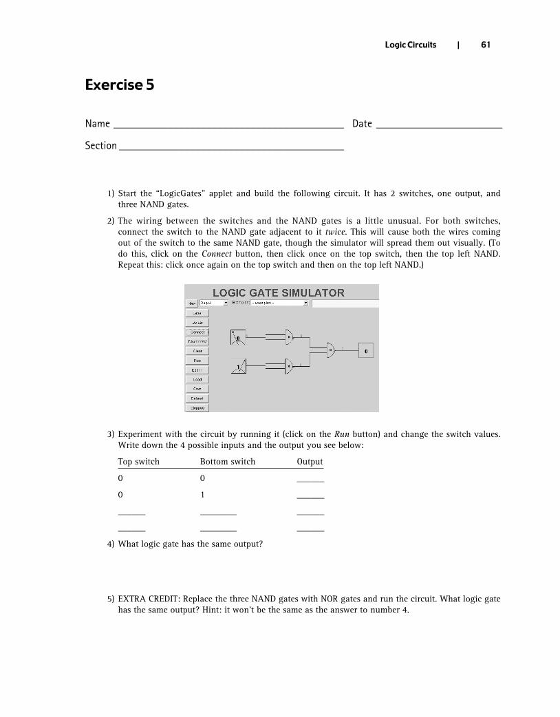
1) Start the “LogicGates” applet and build the following circuit. It has 2 switches, one output, andthree NAND gates.
2) The wiring between the switches and the NAND gates is a little unusual. For both switches,connect the switch to the NAND gate adjacent to it twice. This will cause both the wires comingout of the switch to the same NAND gate, though the simulator will spread them out visually. (Todo this, click on the Connect button, then click once on the top switch, then the top left NAND.Repeat this: click once again on the top switch and then on the top left NAND.)
3) Experiment with the circuit by running it (click on the Run button) and change the switch values.Write down the 4 possible inputs and the output you see below:
Top switch Bottom switch Output
0 0 ______
0 1 ______
______ ________ ______
______ ________ ______
4) What logic gate has the same output?
5) EXTRA CREDIT: Replace the three NAND gates with NOR gates and run the circuit. What logic gatehas the same output? Hint: it won’t be the same as the answer to number 4.
38328_CH04_Meyer.qxd 11/8/05 2:52 PM Page 61

Exercise 6
62 | Laboratory 2
Name __________________________________________ Date _______________________
Section _________________________________________
A lot of students just do not believe DeMorgan’s Law (p. 107 of your textbook) so let’s see if theLogicGates simulator can prove it.
1) Start the “LogicGates” applet.
2) Add 2 switches and arrange them vertically on the left side of the panel. The top one we’ll call Aand the bottom one will be B.
3) We will implement both (AB)’ and (A’ OR B’) in the same circuit. Add two outputs. One output willhave the value of (AB)’ and the other will have the value of (A’ OR B’). If the output boxes read thesame for all inputs, then we know that (AB)’ = (A’ OR B’).
4) Since (AB)’ is just the NAND gate, add one NAND gate and connect both A and B to it. Thenconnect the NAND gate to the top output.
5) For the (A’ OR B’) part, we’ll need two NOT gates, connected to A and B. The output of these NOTgates goes into an OR gate, which then goes into the bottom output.
6) Run through all four combinations of binary values of A and B, writing down the two outputs. Arethey the same? Is DeMorgan’s Law true?
A B Top Output Bottom Output
0 0 ______ ______
0 1 ______ ______
______ ________ ______ ______
______ ________ ______ ______
38328_CH04_Meyer.qxd 11/8/05 2:52 PM Page 62

Exercise 7
Logic Circuits | 63
Name __________________________________________ Date _______________________
Section _________________________________________
In this exercise we will create a simple multiplexer. Pages 110-111 of your textbook describe how amultiplexer selects which input signal will be copied to the output, based on a set of control lines. Ifwe have 8 incoming signals, we need three select control lines, as shown in the book. Four incomingsignals need only 2 select control lines, whereas 2 incoming signals would require only 1. (If you had16 incoming signals, how many select control lines would you need?)
1) Start the “LogicGates” applet. In this circuit, we will create a multiplexor with two inputs and onecontrol wire.
2) Put three switches in the panel and one output. Label one of the switches S0 and the other two D0and D1. The S0 switch should be at the left edge and the D0 at the top, similar to the placement onp. 111. You’ll need an output at the right edge, as shown below.
3) The tricky part is deciding what the logic gates inside the three mystery boxes should be. All threequestion mark gates are either AND or OR. You could experiment until you get it right, but let’sapply a little brainpower.
The value in D0, whether it is a 0 or a 1, should be copied to the output box when the selectcontrol wire has 0 in it. Similarly, the value of D1 must be copied to the output box when S0 hasthe value 1 in it. This is why S0 is called a select control input, because it selects which of the twoDs gets copied.
Our task is to figure out which value of S0 will permit D0 through. However, let’s tackle the easiercase of figuring out which value of S1 will permit D1 through, and then we’ll work backward fromthere.
When S0 is 1, we want D1. If we AND S1 and D1, then the output will be whatever D1 is, whetherit is 0 or 1. But if S0 is 0, then we want D0 and not D1. So our AND gate will ignore D1’s valueand always give us 0.
By reversing our logic, we see that when S0 is 0 we want D0, so what operation do we apply tothem? We can’t quite use the same one as above (AND) because S0 being 0 would always give us0. That is why we have to stick a NOT gate in there. Then S0’ becomes 1 and if we AND that withD0, we get whatever D0’s value is. (Remember that is either 0 or 1. The whole point is to copy D0’svalue through, not force it to be 0 or 1.)
38328_CH04_Meyer.qxd 11/8/05 2:52 PM Page 63

64 | Laboratory 4
Now we have two cases and two sets of gates: when S0 is 0, select D0’s value. WhenS0 is 1, select D1’s value. But we want just one output, not two!
What gate would take 2 or more wires, and “combine” their logic values? You won’tget the answer directly here, so think hard about it. If both inputs are 0, the outputshould be 0. When either input is 1, the output should be 1. Hmmm. . . .
4) Real multiplexors often select between 8, 16, 32, or even more inputs. As your bookshows, the binary number represented by the values on S2S1S0 permit one of eight datavalues to flow through to the final F output. Although our logic gate simulator is alittle too primitive to permit large diagrams, you might try building one with 4 datainputs and two select control wires. You just might be able to squeeze it all in.
38328_CH04_Meyer.qxd 11/8/05 2:52 PM Page 64

Deeper InvestigationThe “LogicGates” applet can create some very complicated circuits. Its main limitationis due to the finite amount of space available—if you have very many gates, you’lleventually run out of room. However, judicious use of the truth table box can cutdown on screen clutter.
Example 5 of the sample circuits in the applet is a model of the S-R latch shownon p. 106 of your textbook. It is called memory latch. Try running it. When it starts,the output boxes will cycle between 0 and 1. To stop that, click on one of the switchesso that it reads 1. Now the circuit is stable. Experiment with it by setting one of theinputs to 1, then changing it back to 0, and watch the outputs change.
S-R latches are 1-bit memories built out of logic gates. Real computer chips usesomething like them in the main CPU for registers and other small, high-speed storage.Because the S-R latch has some serious timing problems, variants of it such as theclocked D-latch are used instead, as are even more complicated circuits called flip-flops.
S-R latches are circuits that have a peculiar characteristic about their wiring. Canyou tell what it is? If not, pretend that the top switch pours a blue-colored liquidthrough the wires and the bottom switch pours a red-colored liquid. Trace the liquidswith colored pens. What do you notice? What would you call this characteristic of S-Rlatch circuits? Your teacher might be able to give you a hint.
Because of this characteristic, circuits like the S-R latch are called sequentialcircuits. The output of sequential circuits depends not just on the current inputs, butalso on the previous values on all the wires. They give a different sequence of resultsover time. Straight-through circuits like the one on p. 105 of your textbook are calledcombinational circuits because their outputs depend only on the combination of theirinput values.
Try to find out more about logic circuits. Look in some hardware books for anexample of a flip-flop circuit. Try tracing its workings.
Logic Circuits | 65
38328_CH04_Meyer.qxd 11/8/05 2:52 PM Page 65

Intentional Blank 6638328_CH04_Meyer.qxd 11/8/05 2:52 PM Page 66


![REVISIÓN DE DISTINTAS IMPLEMENTACIONES PARA …eprints.rclis.org/32783/1/8651589-38328-5-PB.pdf · Campinas, SP v.16 n.2 p. 273-292 mayo/ago. 2018 [274] RESUMEN: Este trabajo relata](https://static.fdocuments.us/doc/165x107/5e36282b0b277609677dc2e8/revisin-de-distintas-implementaciones-para-campinas-sp-v16-n2-p-273-292-mayoago.jpg)