3.3V Powered, 15KV ESD protected, - Digi-Key Sheets/ST Microelectronics PDFS... · 3.3V Powered,...
22
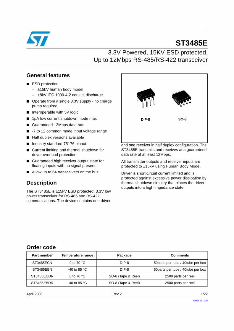
April 2006 Rev 2 1/22 22 ST3485E 3.3V Powered, 15KV ESD protected, Up to 12Mbps RS-485/RS-422 transceiver General features ■ ESD protection – ±15kV human body model – ±8kV IEC 1000-4-2 contact discharge ■ Operate from a single 3.3V supply - no charge pump required ■ Interoperable with 5V logic ■ 1μA low current shutdown mode max ■ Guaranteed 12Mbps data rate ■ -7 to 12 common mode input voltage range ■ Half duplex versions available ■ Industry standard 75176 pinout ■ Current limiting and thermal shutdown for driver overload protection ■ Guaranteed high receiver output state for floating inputs with no signal present ■ Allow up to 64 transceivers on the bus Description The ST3485E is ±15kV ESD protected, 3.3V low power transceiver for RS-485 and RS-422 communications. The device contains one driver and one receiver in half duplex configuration. The ST3485E transmits and receives at a guaranteed data rate of at least 12Mbps. All transmitter outputs and receiver inputs are protected to ±15kV using Human Body Model. Driver is short-circuit current limited and is protected against excessive power dissipation by thermal shutdown circuitry that places the driver outputs into a high-impedance state. DIP-8 SO-8 www.st.com Order code Part number Temperature range Package Comments ST3485ECN 0 to 70 °C DIP-8 50parts per tube / 40tube per box ST3485EBN -40 to 85 °C DIP-8 50parts per tube / 40tube per box ST3485ECDR 0 to 70 °C SO-8 (Tape & Reel) 2500 parts per reel ST3485EBDR -40 to 85 °C SO-8 (Tape & Reel) 2500 parts per reel
-
Upload
hoangkhanh -
Category
Documents
-
view
218 -
download
0
Transcript of 3.3V Powered, 15KV ESD protected, - Digi-Key Sheets/ST Microelectronics PDFS... · 3.3V Powered,...
April 2006 Rev 2 1/22
22
ST3485E 3.3V Powered, 15KV ESD protected,
Up to 12Mbps RS-485/RS-422 transceiver
General features ESD protection
– ±15kV human body model– ±8kV IEC 1000-4-2 contact discharge
Operate from a single 3.3V supply - no charge pump required
Interoperable with 5V logic
1µA low current shutdown mode max
Guaranteed 12Mbps data rate
-7 to 12 common mode input voltage range
Half duplex versions available
Industry standard 75176 pinout
Current limiting and thermal shutdown for driver overload protection
Guaranteed high receiver output state for floating inputs with no signal present
Allow up to 64 transceivers on the bus
DescriptionThe ST3485E is ±15kV ESD protected, 3.3V low power transceiver for RS-485 and RS-422 communications. The device contains one driver
and one receiver in half duplex configuration. The ST3485E transmits and receives at a guaranteed data rate of at least 12Mbps.
All transmitter outputs and receiver inputs are protected to ±15kV using Human Body Model.
Driver is short-circuit current limited and is protected against excessive power dissipation by thermal shutdown circuitry that places the driver outputs into a high-impedance state.
DIP-8 SO-8
www.st.com
Order codePart number Temperature range Package Comments
ST3485ECN 0 to 70 °C DIP-8 50parts per tube / 40tube per box
ST3485EBN -40 to 85 °C DIP-8 50parts per tube / 40tube per box
ST3485ECDR 0 to 70 °C SO-8 (Tape & Reel) 2500 parts per reel
ST3485EBDR -40 to 85 °C SO-8 (Tape & Reel) 2500 parts per reel

Contents ST3485E
2/22
Contents
1 Pin configuration . . . . . . . . . . . . . . . . . . . . . . . . . . . . . . . . . . . . . . . . . . . . 3
2 Truth tables . . . . . . . . . . . . . . . . . . . . . . . . . . . . . . . . . . . . . . . . . . . . . . . . 4
3 Maximum ratings . . . . . . . . . . . . . . . . . . . . . . . . . . . . . . . . . . . . . . . . . . . . 5
4 Electrical characteristics . . . . . . . . . . . . . . . . . . . . . . . . . . . . . . . . . . . . . 6
5 Test circuits and typical characteristics . . . . . . . . . . . . . . . . . . . . . . . . . 9
6 Package mechanical data . . . . . . . . . . . . . . . . . . . . . . . . . . . . . . . . . . . . 17
7 Revision history . . . . . . . . . . . . . . . . . . . . . . . . . . . . . . . . . . . . . . . . . . . 21

ST3485E Pin configuration
3/22
1 Pin configuration
Figure 1. Pin connections
Table 1. Pin description
Pin n° Symbol Name and function
1 RO Receiver output. If A>B by 200mV, RO will be high; if A<B by 200mV, RO will be low
2 REReceiver output enable. RO is enabled when RE is low; RO is high impedance when RE is high. If RE is high and DE is low, the device will enter a low power shutdown mode.
3 DE
Driver output enable. The driver outputs are enabled by bringing DE high. They are high impedance when DE is low. If RE is high DE is low, the device will enter a low-power shutdown mode. If the driver outputs are enabled, the part functions as line driver, while they are high impedance, it functions as line receivers if RE is low.
4 DIDriver input. A low on DI forces output A low and output B high. Similarly, a high on DI forces output A high and output B low
5 GND Ground
6 A Non-inverting receiver input and non-inverting driver output
7 B Inverting receiver input and inverting driver output
8 VCC Supply voltage: VCC= 3V to 3.6V

Truth tables ST3485E
4/22
2 Truth tables
Note: X= Don’t care; Z=High impedance
Note: X= Don’t care; Z=High impedance
Table 2. Truth table (driver)
Inputs OutputsMode
RE DE DI B A
X H H L H Normal
X H L H L Normal
L L X Z Z Normal
H L X Z Z Shutdown
Table 3. Truth table (receiver)
INPUTS OUTPUTMODE
RE DE A-B RO
L L ≥ 0.2V H Normal
L L ≤ -0.2V L Normal
L L Inputs Open H Normal
H L X Z Shutdown

ST3485E Maximum ratings
5/22
3 Maximum ratings
Note: Absolute Maximum Ratings are those values beyond which damage to the device may occur. Functional operation under these condition is not implied.
Table 4. Absolute maximum ratings
Symbol Parameter Value Unit
VCC Supply voltage 7 V
VI Control input voltage (RE, DE) -0.3 to 7 V
VDI Driver input voltage (DI) -0.3 to 7 V
VDO Driver output voltage (A, B) ± 14 V
VRI Receiver input voltage (A, B) ± 14 V
VRO Receiver output voltage (RO) -0.3 to (VCC + 0.3) V
Table 5. ESD Performance: transmitter outputs, receiver inputs
Symbol Parameter Test conditions Min. Typ. Max. Unit
ESD ESD Protection voltage Human body model ± 15 KV
ESD ESD Protection voltage IEC-1000-4-2 Contact discharge ± 8 KV

Electrical characteristics ST3485E
6/22
4 Electrical characteristics
Table 6. Electrical characteristics VCC = 3V to 3.6V, TA = -40 to 85°C, unless otherwise specified. Typical values are referred to TA = 25°C)
Symbol Parameter Test conditions Min. Typ. Max. Unit
ISUPPLY VCC Power supply current No Load, DI=0V or VCC
DE=VCC,RE=0V or VCC
1.3 2.2 mA
DE=0V, RE=0V
1.2 1.9 mA
ISHDN Shutdown supply current DE=0V, RE=VCC, DI=0V or VCC 0.002 1 µA
Table 7. Logic input electrical characteristics VCC = 3V to 3.6V, TA = -40 to 85°C, unless otherwise specified. Typical values are referred to TA = 25°C)
Symbol Parameter Test Conditions Min. Typ. Max. Unit
VIL Input logic threshold low DE, DI, RE 1.3 0.8 V
VIH Input logic threshold high DE, DI, RE 2 V
IIN1 Logic input current DE, DI, RE ± 2.0 µA
IIN2 Input current (A, B) DE=0V, VCC= 0 or 3.6VVIN=12V 1 mA
VIN=-7V -0.8 mA
Table 8. Transmitter electrical characteristics VCC = 3V to 3.6V, TA = -40 to 85°C, unless otherwise specified. Typical values are referred to Ta = 25°C)
Symbol Parameter Test conditions Min. Typ. Max. Unit
VOD Differential drive output
RL= 100Ω (RS-422) (Figure 1.) 2 V
RL= 54Ω (RS-485) (Figure 1.) 1.5 V
RL= 60Ω (RS-485) (Figure 2.) 1.5 V
∆VOD
Change in magnitude of driver differential output voltage for complementary output states (Note: 1)
RL= 54Ω or 100Ω (Figure 1.) 0.2 V
VOCDriver common mode output voltage
RL= 54Ω or 100Ω (Figure 1.) 3 V
∆VOC
Change in magnitude of driver common mode output voltage (Note: 1)
RL= 54Ω or 100Ω (Figure 1.) 0.2 V
IOSDDriver short circuit output current
± 250 mA

ST3485E Electrical characteristics
7/22
Table 9. Receiver electrical characteristics VCC = 3V to 3.6V, TA = -40 to 85°C, unless otherwise specified. Typical values are referred to Ta = 25°C)
Symbol Parameter Test Conditions Min. Typ. Max. Unit
VTHReceiver differential threshold voltage
VCM = -7V to 12V, DE = 0 -0.2 0.2 V
∆VTH Receiver input hysteresis VCM = 0V 70 V
VOHReceiver output high voltage
IOUT = -4mA, VID = 200mV(Figure 8. and Figure 9.)
2 V
VOLReceiver output low voltage
IOUT = 4mA, VID = -200mV, (Figure 3.) 0.4 V
IOZR3-State (high impedance) output current at receiver
VCC = 3.6VVO = 0V to VCC ± 1 µA
RRIN Receiver input resistance VCM = -7V to 12V 24 KΩ
IOSRReceiver short-circuit current
VRO = 0V to VCC 7 60 mA
Table 10. Driver switching characteristics VCC = 3V to 3.6V, TA = -40 to 85°C, unless otherwise specified. Typical values are referred to Ta = 25°C)
Symbol Parameter Test Conditions Min. Typ. Max. Unit
DR Maximum data rate 12 15 Mbps
tDD Differential output delayRL= 60Ω, CL = 15pF, (Figure 4. and Figure 5.)
18 30 ns
tTDDifferential output transition time
RL= 60Ω, CL = 15pF, (Figure 4. and Figure 5.)
12 20 ns
tPLHtPHL
Propagation delay RL= 27Ω, CL = 15pF, (Figure 8. and Figure 9.)
18 30 ns
tPDS|tPLH - tPHL| Propagation delay skew (Note 2)
RL= 27Ω, CL = 15pF, (Figure 8. and Figure 9.)
2 5 ns
tPZL Output enable time RL= 110Ω, (Figure 10. and Figure 11.) 19 35 ns
tPZH Output enable time RL= 110Ω, (Figure 6. and Figure 7.) 30 50 ns
tPHZ Output disable time RL= 110Ω, (Figure 6. and Figure 7.) 19 35 ns
tPLZ Output disable time RL= 110Ω, (Figure 10. and Figure 11.) 30 50 ns
tSKEWDifferential output delay skew
1 3 ns
tZH(SHDN)Driver enable from shutdown to output high
30 50 ns
tZL(SHDN)Driver enable from shutdown to output low
19 35 ns

Electrical characteristics ST3485E
8/22
Note: 1 ∆VOD and ∆VOC are the changes in VOD and VOC, respectively, when the DI input changes state.
2 Measured on |tPLH(A)-tPHL(A)| and |tPLH(B)-tPHL(B)|
3 The transceivers are put into shutdown by bring RE high and DE low. If the input are in state for less than 80ns, the part are guaranteed not to enter shutdown. If the inputs are in this state for at least 300ns, the parts are guaranteed to have entered shutdown.
Table 11. Receiver switching characteristics VCC = 3V to 3.6V, TA = -40 to 85°C, unless otherwise specified. Typical values are referred to Ta = 25°C)
Symbol Parameter Test Conditions Min. Typ. Max. Unit
tPLHtPHL
Propagation delayVID =0V to 3V, CL1 = 15pF(Figure 12. and Figure 13.)
30 50 ns
tRPDS|tPLH - tPHL| Propagation delay skew
VID =0V to 3V, CL1 = 15pF(Figure 12. and Figure 13.)
1 3 ns
tPZL Output enable time CRL = 15pF, (Figure 14. and Figure 18.) 10 20 ns
tPZH Output enable time CRL = 15pF, (Figure 14. and Figure 18.) 10 20 ns
tPHZ Output disable time CRL = 15pF, (Figure 14. and Figure 18.) 10 20 ns
tPLZ Output disable time CRL = 15pF, (Figure 14. and Figure 18.) 10 20 ns
tZH(SHDN)Receiver enable from shutdown to output high
CRL = 15pF, (Figure 14. and Figure 18.) 10 20 ns
tZL(SHDN)Receiver enable from shutdown to output low
CRL = 15pF, (Figure 14. and Figure 18.) 20 40 µs

ST3485E Test circuits and typical characteristics
9/22
5 Test circuits and typical characteristics
Figure 2. Driver and VOC test load
Figure 3. Driver VOD with varying common mode voltage test load
Figure 4. Receiver VOH and VOL test circuit
Test circuits and typical characteristics ST3485E
10/22
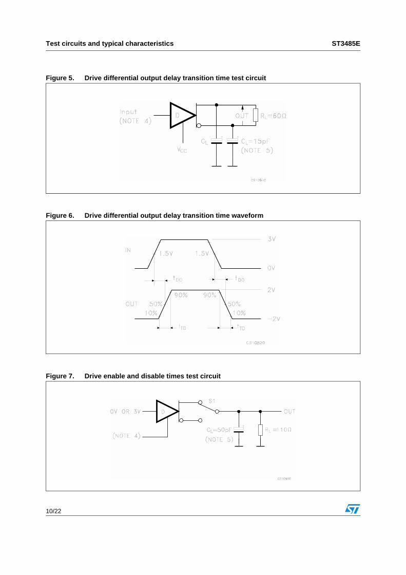
Figure 5. Drive differential output delay transition time test circuit
Figure 6. Drive differential output delay transition time waveform
Figure 7. Drive enable and disable times test circuit

ST3485E Test circuits and typical characteristics
11/22
Figure 8. Drive enable and disable times waveforms
Figure 9. Drive propagation time test circuit
Figure 10. Drive propagation time waveform
Test circuits and typical characteristics ST3485E
12/22
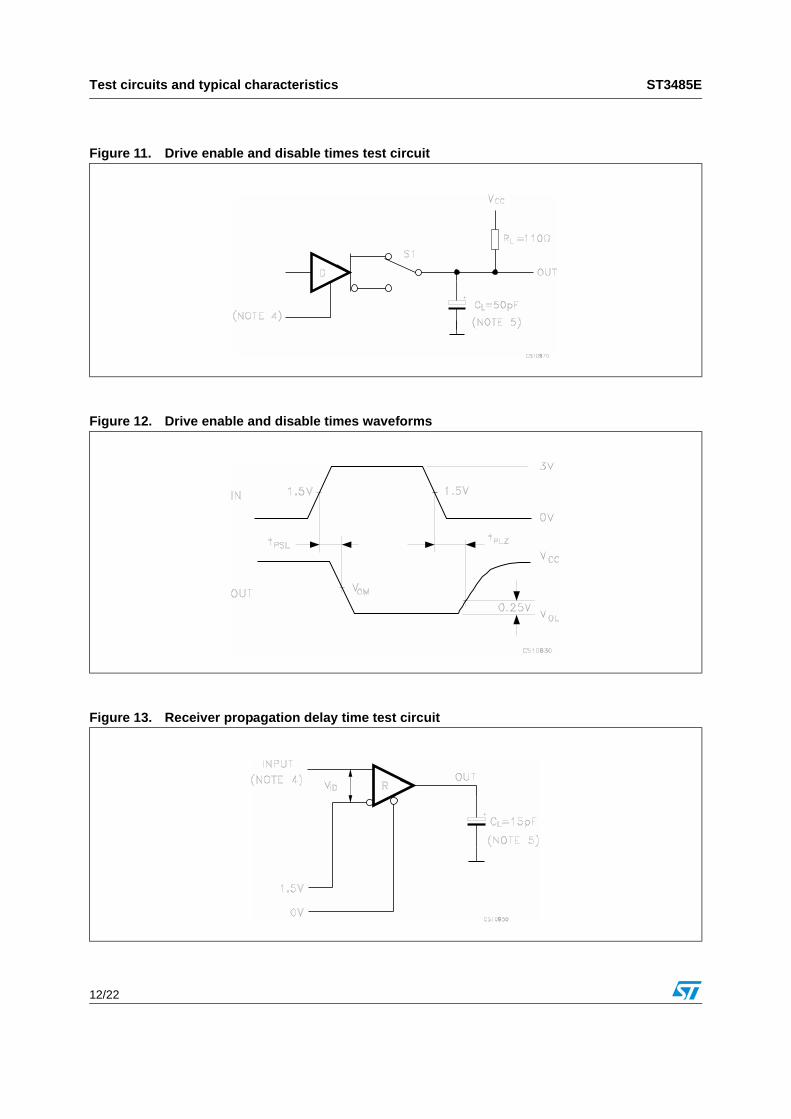
Figure 11. Drive enable and disable times test circuit
Figure 12. Drive enable and disable times waveforms
Figure 13. Receiver propagation delay time test circuit
ST3485E Test circuits and typical characteristics
13/22
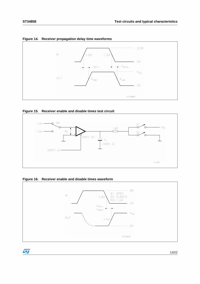
Figure 14. Receiver propagation delay time waveforms
Figure 15. Receiver enable and disable times test circuit
Figure 16. Receiver enable and disable times waveform

Test circuits and typical characteristics ST3485E
14/22
Figure 17. Receiver enable and disable times waveform
Figure 18. Receiver enable and disable times waveform
Figure 19. Receiver enable and disable times waveform

ST3485E Test circuits and typical characteristics
15/22
Figure 20. Receiver output current vs output
low voltage Figure 21. Receiver output current vs output
high voltage
Figure 22. Low level driver output capability Figure 23. High level driver output capability
Figure 24. Receiver input characteristics Figure 25. Driver short circuit current
Test circuits and typical characteristics ST3485E
16/22
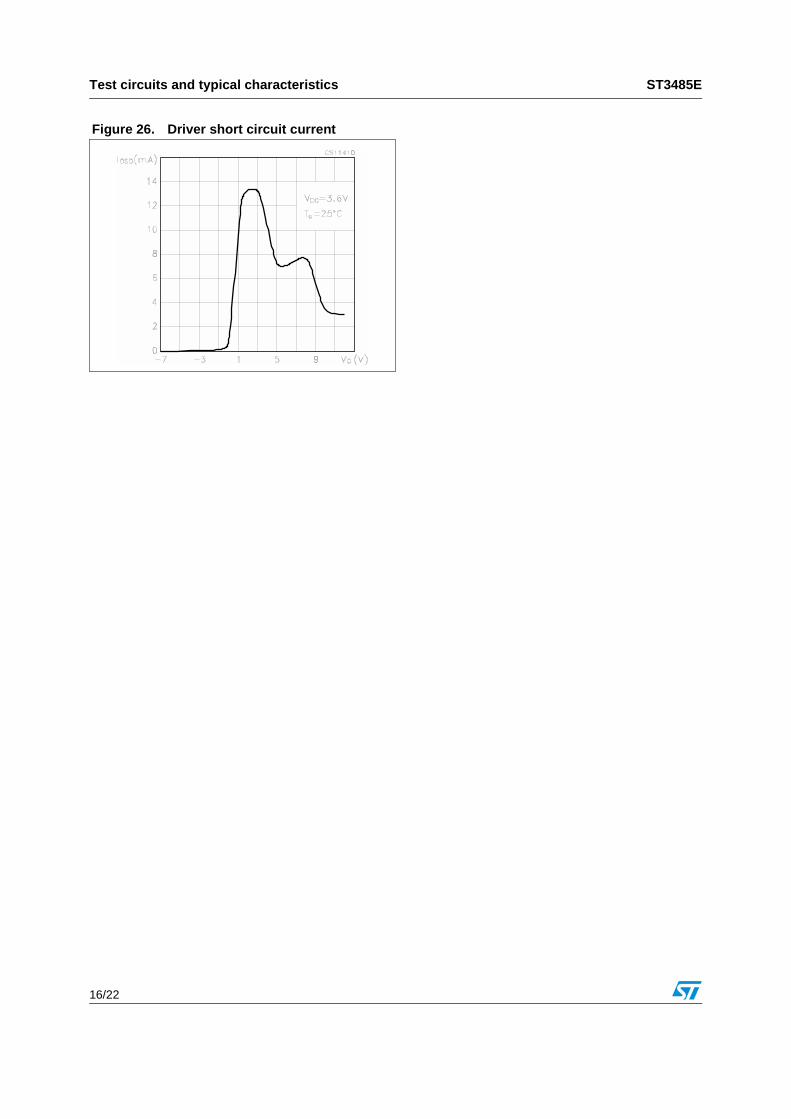
Figure 26. Driver short circuit current

ST3485E Package mechanical data
17/22
6 Package mechanical data
In order to meet environmental requirements, ST offers these devices in ECOPACK® packages. These packages have a Lead-free second level interconnect. The category of second level interconnect is marked on the package and on the inner box label, in compliance with JEDEC Standard JESD97. The maximum ratings related to soldering conditions are also marked on the inner box label. ECOPACK is an ST trademark. ECOPACK specifications are available at: www.st.com

Package mechanical data ST3485E
18/22
DIM.mm. inch
MIN. TYP MAX. MIN. TYP. MAX.
A 3.3 0.130
a1 0.7 0.028
B 1.39 1.65 0.055 0.065
B1 0.91 1.04 0.036 0.041
b 0.5 0.020
b1 0.38 0.5 0.015 0.020
D 9.8 0.386
E 8.8 0.346
e 2.54 0.100
e3 7.62 0.300
e4 7.62 0.300
F 7.1 0.280
I 4.8 0.189
L 3.3 0.130
Z 0.44 1.6 0.017 0.063
Plastic DIP-8 MECHANICAL DATA
P001F
ST3485E Package mechanical data
19/22
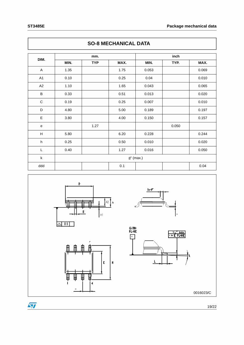
DIM.mm. inch
MIN. TYP MAX. MIN. TYP. MAX.
A 1.35 1.75 0.053 0.069
A1 0.10 0.25 0.04 0.010
A2 1.10 1.65 0.043 0.065
B 0.33 0.51 0.013 0.020
C 0.19 0.25 0.007 0.010
D 4.80 5.00 0.189 0.197
E 3.80 4.00 0.150 0.157
e 1.27 0.050
H 5.80 6.20 0.228 0.244
h 0.25 0.50 0.010 0.020
L 0.40 1.27 0.016 0.050
k ° (max.)
ddd 0.1 0.04
SO-8 MECHANICAL DATA
0016023/C
8

Package mechanical data ST3485E
20/22
DIM.mm. inch
MIN. TYP MAX. MIN. TYP. MAX.
A 330 12.992
C 12.8 13.2 0.504 0.519
D 20.2 0.795
N 60 2.362
T 22.4 0.882
Ao 8.1 8.5 0.319 0.335
Bo 5.5 5.9 0.216 0.232
Ko 2.1 2.3 0.082 0.090
Po 3.9 4.1 0.153 0.161
P 7.9 8.1 0.311 0.319
Tape & Reel SO-8 MECHANICAL DATA
ST3485E Revision history
21/22
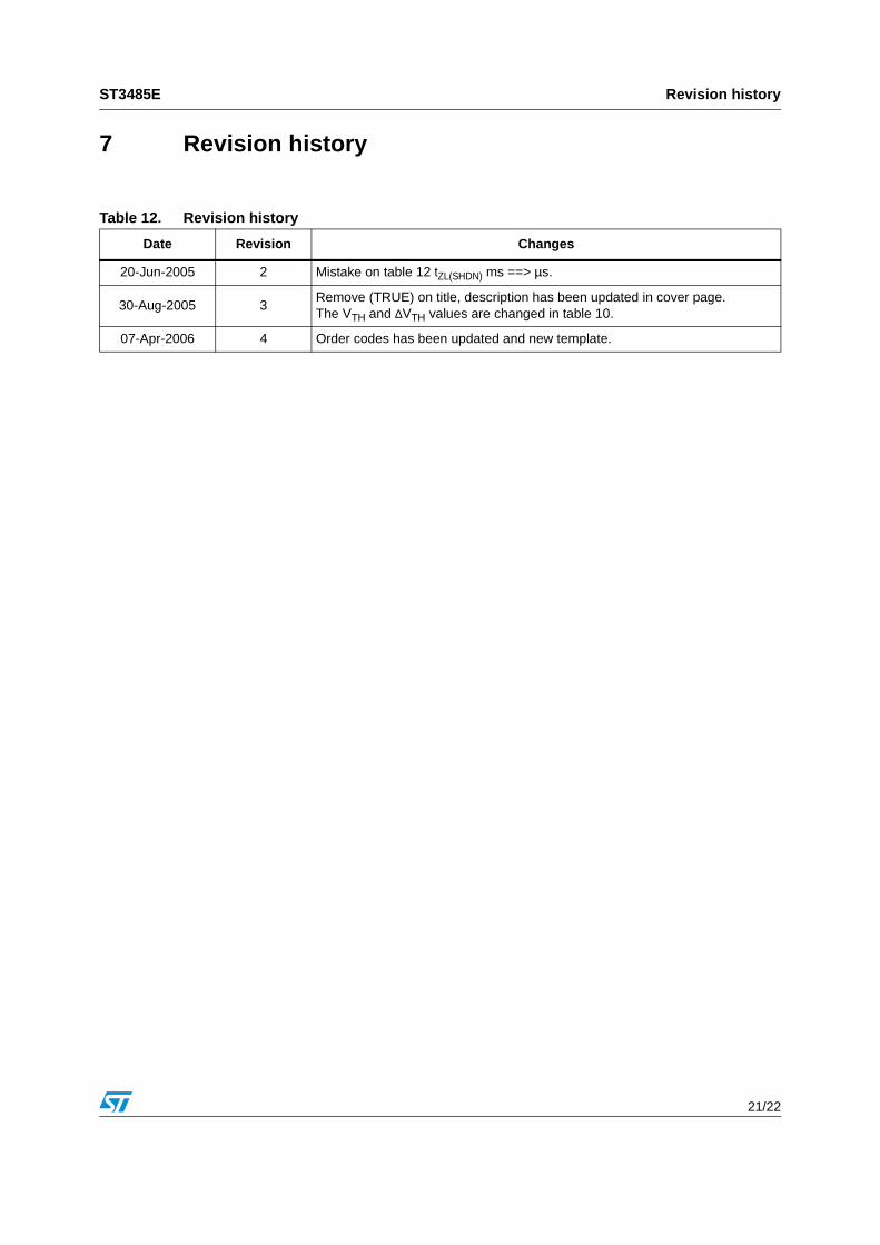
7 Revision history
Table 12. Revision history
Date Revision Changes
20-Jun-2005 2 Mistake on table 12 tZL(SHDN) ms ==> µs.
30-Aug-2005 3Remove (TRUE) on title, description has been updated in cover page.The VTH and ∆VTH values are changed in table 10.
07-Apr-2006 4 Order codes has been updated and new template.

ST3485E
22/22
Please Read Carefully:
Information in this document is provided solely in connection with ST products. STMicroelectronics NV and its subsidiaries (“ST”) reserve theright to make changes, corrections, modifications or improvements, to this document, and the products and services described herein at anytime, without notice.
All ST products are sold pursuant to ST’s terms and conditions of sale.
Purchasers are solely responsible for the choice, selection and use of the ST products and services described herein, and ST assumes noliability whatsoever relating to the choice, selection or use of the ST products and services described herein.
No license, express or implied, by estoppel or otherwise, to any intellectual property rights is granted under this document. If any part of thisdocument refers to any third party products or services it shall not be deemed a license grant by ST for the use of such third party productsor services, or any intellectual property contained therein or considered as a warranty covering the use in any manner whatsoever of suchthird party products or services or any intellectual property contained therein.
UNLESS OTHERWISE SET FORTH IN ST’S TERMS AND CONDITIONS OF SALE ST DISCLAIMS ANY EXPRESS OR IMPLIEDWARRANTY WITH RESPECT TO THE USE AND/OR SALE OF ST PRODUCTS INCLUDING WITHOUT LIMITATION IMPLIEDWARRANTIES OF MERCHANTABILITY, FITNESS FOR A PARTICULAR PURPOSE (AND THEIR EQUIVALENTS UNDER THE LAWSOF ANY JURISDICTION), OR INFRINGEMENT OF ANY PATENT, COPYRIGHT OR OTHER INTELLECTUAL PROPERTY RIGHT.
UNLESS EXPRESSLY APPROVED IN WRITING BY AN AUTHORIZE REPRESENTATIVE OF ST, ST PRODUCTS ARE NOT DESIGNED,AUTHORIZED OR WARRANTED FOR USE IN MILITARY, AIR CRAFT, SPACE, LIFE SAVING, OR LIFE SUSTAINING APPLICATIONS,NOR IN PRODUCTS OR SYSTEMS, WHERE FAILURE OR MALFUNCTION MAY RESULT IN PERSONAL INJURY, DEATH, ORSEVERE PROPERTY OR ENVIRONMENTAL DAMAGE.
Resale of ST products with provisions different from the statements and/or technical features set forth in this document shall immediately voidany warranty granted by ST for the ST product or service described herein and shall not create or extend in any manner whatsoever, anyliability of ST.
ST and the ST logo are trademarks or registered trademarks of ST in various countries.
Information in this document supersedes and replaces all information previously supplied.
The ST logo is a registered trademark of STMicroelectronics. All other names are the property of their respective owners.
© 2006 STMicroelectronics - All rights reserved
STMicroelectronics group of companies
Australia - Belgium - Brazil - Canada - China - Czech Republic - Finland - France - Germany - Hong Kong - India - Israel - Italy - Japan - Malaysia - Malta - Morocco - Singapore - Spain - Sweden - Switzerland - United Kingdom - United States of America
www.st.com