3.3 VOLT TIME SLOT INTERCHANGE DIGITAL SWITCH 1,024 x …
20
1 2005 Integrated Device Technology, Inc. All rights reserved. Product specifications subject to change without notice. DSC-5714/4 © JANUARY 2005 3.3 VOLT TIME SLOT INTERCHANGE DIGITAL SWITCH 1,024 x 1,024 IDT72V70210 IDT and the IDT logo are trademarks of Integrated Device Technology, Inc. The ST-BUS ® is a trademari of Mitel Corp. FUNCTIONAL BLOCK DIAGRAM FEATURES: • 32 serial input and output streams • 1,024 x 1,024 channel non-blocking switching at 2.048 Mb/s • Per-channel Variable Delay Mode for low-latency applications • Per-channel Constant Delay Mode for frame integrity applications • Automatic identification of ST-BUS ® and GCI serial streams • Automatic frame offset delay measurement • Per-stream frame delay offset programming • Per-channel high impedance output control • Per-channel processor mode to allow microprocessor writes to TX streams • Direct microprocessor access to all internal memories • Memory block programming for quick set-up • IEEE-1149.1 (JTAG) Test Port • Internal Loopback for testing •· Available in 144-pin Ball Grid Array (BGA) and 144-pin Thin Quad Flatpack (TQFP) packages • Operating Temperature Range -40°C to +85°C • 3.3V I/O with 5V tolerant inputs and TTL compatible outputs DESCRIPTION: The IDT72V70210 has a non-blocking switch capacity of 1,024 x 1,024 channels at 2.048 Mb/s. With 32 inputs and 32 outputs, programmable per stream control, and a variety of operating modes the IDT72V70210 is designed for the TDM time slot interchange function in either voice or data applications. Some of the main features of the IDT72V70210 are low power 3.3 Volt operation, automatic ST-BUS ® /GCI sensing, memory block programming, simple microprocessor interface, one cycle direct internal memory accesses, JTAG Test Access Port (TAP) and per stream programmable input offset delay, variable or constant throughput modes, internal loopback, output enable, and Processor Mode. Output MUX Receive Serial Data Streams RX0 RX1 RX2 RX3 RX4 RX5 RX6 RX7 ODE F0i Vcc CS DS R/W A0-A11 GND DTA D0-D15 5714 drw01 RX8 RX9 RX10 RX11 RX12 RX13 RX14 RX15 Loopback Test Port Data Memory Internal Registers Microprocessor Interface Timing Unit TX0 TX1 TX2 TX3 TX4 TX5 TX6 TX7 TX8 TX9 TX10 TX11 TX12 TX13 TX14 TX15 CLK FE IC TDI TMS TCK TDO TRST RESET RX16 RX17 RX18 RX19 RX20 RX21 RX22 RX23 RX24 RX25 RX26 RX27 RX28 RX29 RX30 RX31 TX16 TX17 TX18 TX19 TX20 TX21 TX22 TX23 TX24 TX25 TX26 TX27 TX28 TX29 TX30 TX31 Connection Memory Transmit Serial Data Streams
Transcript of 3.3 VOLT TIME SLOT INTERCHANGE DIGITAL SWITCH 1,024 x …
1 2005 Integrated Device Technology, Inc. All rights reserved. Product specifications subject to change without notice. DSC-5714/4©
JANUARY 2005
3.3 VOLT TIME SLOT INTERCHANGEDIGITAL SWITCH1,024 x 1,024
IDT72V70210
IDT and the IDT logo are trademarks of Integrated Device Technology, Inc. The ST-BUS® is a trademari of Mitel Corp.
FUNCTIONAL BLOCK DIAGRAM
FEATURES:••••• 32 serial input and output streams••••• 1,024 x 1,024 channel non-blocking switching at 2.048 Mb/s••••• Per-channel Variable Delay Mode for low-latency applications••••• Per-channel Constant Delay Mode for frame integrity applications••••• Automatic identification of ST-BUS® and GCI serial streams••••• Automatic frame offset delay measurement••••• Per-stream frame delay offset programming••••• Per-channel high impedance output control••••• Per-channel processor mode to allow microprocessor writes to
TX streams••••• Direct microprocessor access to all internal memories••••• Memory block programming for quick set-up••••• IEEE-1149.1 (JTAG) Test Port••••• Internal Loopback for testing•••••· Available in 144-pin Ball Grid Array (BGA) and 144-pin Thin Quad
Flatpack (TQFP) packages••••• Operating Temperature Range -40°°°°°C to +85°°°°°C••••• 3.3V I/O with 5V tolerant inputs and TTL compatible outputs
DESCRIPTION:The IDT72V70210 has a non-blocking switch capacity of 1,024 x 1,024
channels at 2.048 Mb/s. With 32 inputs and 32 outputs, programmable perstream control, and a variety of operating modes the IDT72V70210 is designedfor the TDM time slot interchange function in either voice or data applications.
Some of the main features of the IDT72V70210 are low power 3.3 Voltoperation, automatic ST-BUS®/GCI sensing, memory block programming,simple microprocessor interface, one cycle direct internal memory accesses,JTAG Test Access Port (TAP) and per stream programmable input offset delay,variable or constant throughput modes, internal loopback, output enable, andProcessor Mode.
Output MUX
ReceiveSerial Data Streams
RX0RX1RX2RX3RX4RX5RX6RX7
ODE
F0i
Vcc
CSDS R/W A0-A11
GND
DTA D0-D15
5714 drw01
RX8RX9
RX10RX11RX12RX13RX14RX15
Loopback
Test Port
Data Memory
InternalRegisters
Microprocessor InterfaceTiming Unit
TX0TX1TX2TX3TX4TX5TX6TX7TX8TX9TX10TX11TX12TX13TX14TX15
CLK FE IC
TDITMS TCKTDO TRSTRESET
RX16RX17RX18RX19RX20RX21RX22RX23RX24RX25RX26RX27RX28RX29RX30RX31
TX16TX17TX18TX19TX20TX21TX22TX23TX24TX25TX26TX27TX28TX29TX30TX31
Connection Memory
TransmitSerial Data Streams
rdvorak
Rectangle
rdvorak
Typewritten Text
Thin Quad Flatpack (TQFP)
rdvorak
Typewritten Text
rdvorak
Typewritten Text
rdvorak
Rectangle

2
COMMERCIAL TEMPERATURE RANGEIDT72V70210 3.3V TIME SLOT INTERCHANGEDIGITAL SWITCH 1,024 x 1,024
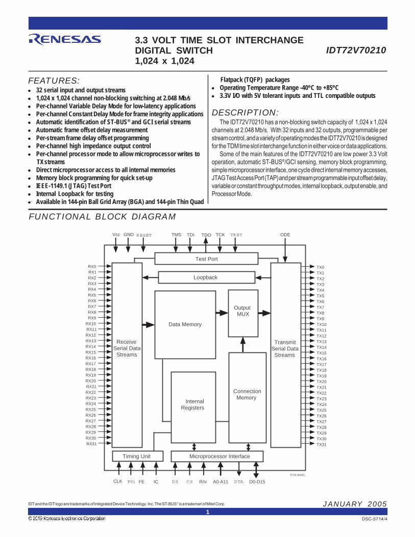
PIN CONFIGURATIONS
RX0 RX1 RX3 RX6 TX1 TX4 TX7 RX10 RX12 RX15 TX10 TX11
CLK ODE RX2 RX5 TX0 TX3 TX6 RX9 RX13
RX14 TX9 TX12
F0i FE RESET RX4 RX7 TX2 TX5 RX8 RX11 TX8 TX13 TX14
TMS IC TDI GND VCC VCC VCC VCC VCC TX15 RX16 RX17
TD0 TCK TRST VCC RX19 RX20 RX21
DS CS R/W VCC RX22 RX23 RX18
A0 A1 A2 VCC TX16 TX17 TX18
A3 A4 A5 VCC TX19 TX20 TX21
A6 A7 A8 D15 TX22 RX24 TX23
A9 A10 DTA D9 D6 D3 D0 TX29 TX26 RX27 RX25 RX26
A11 D12 D11 D7 D4 D1 TX30 TX27 TX24 RX28 RX29
D14 D13 D10 D8 D5 D2 TX31 TX28 TX25 RX31 RX30
A1 BALL PAD CORNER
A
B
C
D
E
F
G
H
J
K
L
M
1 2 3 4 5 6 7 8 9 10 11 125714 drw 02
GND GND GND GND VCC
GND GND GND GND VCC
VCC
GND
GND GND GND VCC
VCC VCC VCC VCC GND
GND
GND GND GND
IC
IC
BGA: 1mm pitch, 13mm x 13mm (BC144-1, order code: BC)TOP VIEW
NOTE:1. All I/O pins are 5V tolerant except for TMS, TDI and TRST.
3
COMMERCIAL TEMPERATURE RANGEIDT72V70210 3.3V TIME SLOT INTERCHANGEDIGITAL SWITCH 1,024 x 1,024
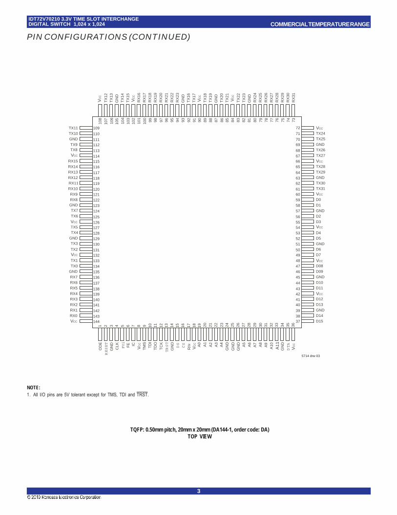
TX11TX10GNDTX9TX8VCC
RX15RX14RX13RX12RX11RX10RX9RX8GNDTX7TX6
TX5TX4
GNDTX3
TX2
TX1TX0
GNDRX7RX6RX5RX4RX3RX2RX1RX0
RX
31R
X30
RX
29R
X28
RX
27R
X26
RX
25R
X24
GN
DT
X23
TX
22
TX
21T
X20
GN
DT
X19
TX
18
TX
17T
X16
GN
DR
X23
RX
22R
X21
RX
20R
X19
RX
18R
X17
RX
16
TX
15T
X14
GN
DT
X13
TX
12
VCC
TX24TX25GNDTX26TX27
TX28TX29GNDTX30TX31
D0D1GNDD2D3
D4D5GNDD6D7
VCC
D08D09GNDD10D11
VCC
D12D13GNDD14D15
DTA
GN
DA
11A
10A9
A8
A7
A6
A5
A4
A3
A2
A1
A0
GN
D
R/WCS
DS
GN
DTRST
TC
K
TD
OT
DI
TM
SV
CCICFE
F0i
CLK
GN
DRESET
OD
E
GN
D
GN
D
5714 drw 03
1 2 3 4 5 6 7 8 9 10 11 12 13 14 15 16 17 18 19 20 21 22 23 24 25 26 27 28 29 30 31 32 33 34 35 36
108
107
106
105
104
103
102
101
100
99 98 97 96 95 94 93 92 91 90 89 88 87 86 85 84 83 82 81 80 79 78 77 76 75 74 73
109
110
111112
113114115116
117118119
120121122123124
125126127128129130
131132133134135136
137
138139140141
142143144
72
71
7069
68676665
646362
6160595857
565554535251
504948474645
44
43424140
393837
VCC
VCC
VCC
VC
C
VC
C
VCC
VCC
VCC
VC
C
VC
C
VC
C
VC
C
TQFP: 0.50mm pitch, 20mm x 20mm (DA144-1, order code: DA)TOP VIEW
NOTE:1. All I/O pins are 5V tolerant except for TMS, TDI and TRST.
PIN CONFIGURATIONS (CONTINUED)

4
COMMERCIAL TEMPERATURE RANGEIDT72V70210 3.3V TIME SLOT INTERCHANGEDIGITAL SWITCH 1,024 x 1,024
PIN DESCRIPTIONSYMBOL NAME I/O DESCRIPTION
GND Ground. Ground Rail.
VCC VCC +3.3 Volt Power Supply.
TX0-31 TX Output 0 to 31 O Serial data output stream. These streams have a data rate of 2.048 Mb/s.(Three-state Outputs)
RX0-31 RX Input 0 to 31 I Serial data input stream. These streams have a data rate of 2.048 Mb/s.
F0i Frame Pulse I This input accepts and automatically identifies frame synchronization signals formatted according toST-BUS® and GCI specifications.
FE Frame Evaluation I This pin is the frame measurement input.
CLK Clock I Serial clock for shifting data in/out on the serial streams (RX/TX 0-31). This input accepts a 4.096 MHz clock.
TMS Test Mode Select I JTAG signal that controls the state transitions of the TAP controller. This pin is pulled HIGH by an internalpull-up when not driven.
TDI Test Serial Data In I JTAG serial test instructions and data are shifted in on this pin. This pin is pulled HIGH by an internal pull-upwhen not driven.
TDO Test Serial Data Out O JTAG serial data is output on this pin on the falling edge of TCK. This pin is held in high-impedance state whenJTAG scan is not enabled.
TCK Test Clock I Provides the clock to the JTAG test logic.
TRST Test Reset I Asynchronously initializes the JTAG TAP controller by putting it in the Test-Logic-reset state. This pin is pulledby an internal pull-up when not driven. This pin should be pulsed LOW on power-up, or held LOW, to ensurethat the IDT72V70210 is in the normal functional mode.
RESET Device Reset I This input (active LOW) puts the IDT72V70210 in its reset state that clears the device internal counters,(Schmitt Trigger Input) registers and brings TX0-31 and microport data outputs to a high-impedance state. The time constant for a
power up reset circuit must be a minimum of five times the rise time of the power supply. In normal operation,the RESET pin must be held LOW for a minimum of 100ns to reset the device.
DS Data Strobe I This active LOW input works in conjunction with CS to enable the read and write operations.
R/W Read/Write I This input controls the direction of the data bus lines during a microprocessor access.
CS Chip Select I Active LOW input used by a microprocessor to activate the microprocessor port of IDT72V70210.
A0-11 Address Bus 0 to 11 I These pins allow direct access to Connection Memory, Data Memory and internal control registers.
D0-15 Data Bus 0-15 I/O These pins are the data bits of the microprocessor port.
DTA Data Transfer O This active LOW signal indicates that a data bus transfer is complete. When the bus cycle ends, this pin drivesAcknowledgment HIGH and then goes high-impedance, allowing for faster bus cycles with a weaker pull-up resistor. A pull-up
resistor is required to hold a HIGH level when the pin is in high-impedance.
ODE Output Drive Enable I This is the output enable control for the TX0-31 serial outputs. When ODE input is LOW and the OSB bit ofthe CR register is LOW, TX0-31 are in a high-impedance state. If this input is HIGH, the TX0-31 outputdrivers are enabled. However, each channel may still be put into a high-impedance state by using the perchannel control bit in the connection memory.
IC Internal Connection I This pin tied to Ground for normal/JTAG operations
5
COMMERCIAL TEMPERATURE RANGEIDT72V70210 3.3V TIME SLOT INTERCHANGEDIGITAL SWITCH 1,024 x 1,024
DESCRIPTION (CONTINUED):The IDT72V70210 is capable of switching up to 1,024 x 1,024 channels
without blocking. Designed to switch 64 Kbit/s PCM or N x 64 Kbit/s data, thedevice maintains frame integrity in data applications and minimizes throughputdelay for voice applications on a per channel basis.
The 32 serial input streams (RX) of the IDT72V70210 can be run 2.048 Mb/sallowing 32 channels per 125μs frame. The data rates on the output streams(TX) are identical to those on the input stream.
With two main operating modes, Processor Mode and Connection Mode,the IDT72V70210 can easily switch data from incoming serial streams (DataMemory) or from the controlling microprocessor (Connection Memory). Ascontrol and status information is critical in data transmission, the Processor Modeis especially useful when there are multiple devices sharing the input and outputstreams.
With data coming from multiple sources and through different paths, dataentering the device is often delayed. To handle this problem, the IDT72V70210has a frame evaluation feature to allow individual streams to be offset from theframe pulse in half clock-cycle intervals up to +4.5 clock cycles.
The IDT72V70210 also provides a JTAG test access port, an internalloopback feature, memory block programming, a simple microprocessorinterface and automatic ST-BUS®/GCI sensing to shorten setup time, aid indebugging and ease use of the device without sacrificing capabilities.
FUNCTIONAL DESCRIPTIONDATA AND CONNECTION MEMORY
All data that comes in through the RX inputs go through a serial-to-parallel conversion before being stored into internal Data Memory. The 8 KHzframe pulse (F0i) is used to mark the 125μs frame boundaries and to sequentiallyaddress the input channels in Data Memory.
Data output on the TX streams may come from either the Serial Input Streams,RX0-31, (Data Memory) or from the microprocessor (Connection Memory). Inthe case that RX input data is to be output, the addresses in connection memoryare used to specify a stream and channel of the input. The connection memoryis setup in such a way that each location corresponds to an output channel foreach particular stream. In that way, more than one channel can output the samedata.
In Processor Mode, the microprocessor writes data to the connectionmemory locations corresponding to the stream and channel that is to beoutput. The lower half (8 least significant bits) of the connection memoryis output every frame until the microprocessor changes the data or modeof the channel. By using this Processor Mode capability, the microproces-sor can access input and output time-slots on a per channel basis.
The four most significant bits of the connection memory are used to controlper channel functions of the out put streams. Specifically, there are bits forProcessor or Connection mode, Constant or Variable delay, enables ordisables of output drivers, and controls for the Loopback function.
If the per channel OE is set to zero, only that particular channel (8-bits) willbe in the high-impedance state. If however, the ODE input pin is low or the OutputStandby Bit (OSB) in the Control Register is low, all of the outputs will be in ahigh-impedance state even if a particular channel in connection memory hasenabled the output for that channel. In other words, the ODE pin and OSB controlbit are master output enables for the device (Table 3).
SERIAL DATA INTERFACE TIMINGThe master clock frequency must always be twice the data rate. For a serial
data rates of 2.048 Mb/s, the master clock (CLK) must be at 4.096 MHz. Theinput and output stream data rates will always be identical.
The IDT72V70210 provides two different interface timing modes, ST-BUS®
or GCI. The IDT72V70210 automatically detects the presence of an input framepulse and identifies it as either ST-BUS® or GCI. In ST-BUS® format, everysecond falling edge of the master clock marks a bit boundary and the data isclocked in on the rising edge of CLK, three quarters of the way into the bit cell.In GCI format, every second rising edge of the master clock marks the bitboundary and data is clocked in on the falling edge of CLK at three quarters ofthe way into the bit cell.
INPUT FRAME OFFSET SELECTIONInput frame offset selection allows the channel alignment of individual
input streams to be offset with respect to the output stream channelalignment (i.e. F0i). Although all input data comes in at the same speed, delayscan be caused by variable path serial backplanes and variable path lengthswhich may be implemented in large centralized and distributed switchingsystems. Because data is often delayed this feature is useful in compensatingfor the skew between clocks.
Each input stream can have its own delay offset value by programming theframe input offset registers (FOR, Table 8). The maximum allowable skew is +4master clock (CLK) periods forward with a resolution of 1/2 clock period. Theoutput frame offset cannot be offset or adjusted.
SERIAL INPUT FRAME ALIGNMENT EVALUATIONThe IDT72V70210 provides the frame evaluation (FE) input to deter-
mine different data input delays with respect to the frame pulse F0i.A measurement cycle is started by setting the start frame evaluation (SFE)
bit low for at least one frame. When the SFE bit in the Control Register is changedfrom low to high, the evaluation starts. Two frames later, the complete frameevaluation (CFE) bit of the frame alignment register (FAR) changes from lowto high to signal that a valid offset measurement is ready to be read from bits 0to 11 of the FAR register. The SFE bit must be set to zero before a newmeasurement cycle is started.
In ST-BUS® mode, the falling edge of the frame measurement signal (FE)is evaluated against the falling edge of the ST-BUS® frame pulse. In GCI mode,the rising edge of FE is evaluated against the rising edge of the GCI frame pulse.See Table 7 and Figure 1 for the description of the frame alignment register.
MEMORY BLOCK PROGRAMMINGThe IDT72V70210 provides users with the capability of initializing the entire
connection memory block in two frames. To set bits 12 to 15 of every connectionmemory location, first program the desired pattern in bits 5 to 8 of the ControlRegister.
The block programming mode is enabled by setting the memory blockprogram (MBP) bit of the control register high. When the block programmingenable (BPE) bit of the Control Register is set to high, the block programmingdata will be loaded into the bits 12 to 15 of every connection memory location.The other connection memory bits (bit 0 to bit 11) are loaded with zeros. Whenthe memory block programming is complete, the device resets the BPE bit to zero.
LOOPBACK CONTROLThe loopback control (LPBK) bit of each connection memory location allows
the TX output data to be looped backed internally to the RX input for diagnosticpurposes.
If the LPBK bit is high, the associated TX output channel data is internallylooped back to the RX input channel (i.e., data from TXn channel m routes tothe RXn channel m internally); if the LPBK bit is low, the loopback feature is

6
COMMERCIAL TEMPERATURE RANGEIDT72V70210 3.3V TIME SLOT INTERCHANGEDIGITAL SWITCH 1,024 x 1,024
disabled. For proper per-channel loopback operation, the contents of framedelay offset registers must be set to zero.
DELAY THROUGH THE IDT72V70210The switching of information from the input serial streams to the output
serial streams results in a throughput delay. The device can be pro-grammed to perform time-slot interchange functions with different through-put delay capabilities on a per-channel basis. For voice applications,variable throughput delay is best as it ensure minimum delay between inputand output data. In wideband data applications, constant throughput delayis best as the frame integrity of the information is maintained through theswitch.
The delay through the device varies according to the type of throughputdelay selected in the V/C bit of the connection memory.
VARIABLE DELAY MODE (V/C BIT = 0)In this mode, the delay is dependent only on the combination of source
and destination channels and is independent of input and output streams.The minimum delay achievable in the IDT72V70210 is three time-slots. Ifthe input channel data is switched to the same output channel (channel n,frame p), it will be output in the following frame (channel n, frame p+1). Thesame is true if the input channel n is switched to output channel n+1 or n+2.If the input channel n is switched to output channel n+3, n+4,..., the newoutput data will appear in the same frame. Table 2 shows the possibledelays for the IDT72V70210 in the variable delay mode.
CONSTANT DELAY MODE (V/C BIT = 1)In this mode, frame integrity is maintained in all switching configurations by
making use of a multiple data memory buffer. Input channel data is written intothe data memory buffers during frame n will be read out during frame n+2. Inthe IDT72V70210, the minimum throughput delay achievable in the constantdelay mode will be one frame. For example, when input time-slot 31 is switchedto output time-slot 0. The maximum delay of 94 time-slots of delay occurs whentime-slot 0 in a frame is switched to time-slot 31 in the frame.
MICROPROCESSOR INTERFACEThe IDT72V70210’s microprocessor interface looks like a standard RAM
interface to improve integration into a system. With a 12-bit address bus anda 16-bit data bus, read and writes are mapped directly into Data and Connectionmemories and require only one cycle to access. By allowing the internalmemories to be randomly accessed in one cycle, the controlling microprocessorhas more time to manage other peripheral devices and can more easily andquickly gather information and setup the switch paths.
Table 4 shows the mapping of the addresses into internal memory blocksand Table 5 shows the Control Register information.
MEMORY MAPPINGThe address bus on the microprocessor interface selects the internal
registers and memories of the IDT72V70210.
The two most significant bits of the address select between the registers, DataMemory, and Connection Memory. If A11 and A10 are HIGH, A9-A0 are usedto address the Data Memory. If A11 is HIGH and A10 is LOW, A9-A0 are usedto address Connection Memory. If A11 is LOW and A10 is HIGH A9-A0 areused to select the Control Register, Frame Alignment Register, and Frame OffsetRegisters. See Table 4 for mappings.
As explained in the Serial Data Interface Timing and Switching Configura-tions sections, after system power-up, the Control Register should be pro-grammed immediately to establish the desired switching configuration.
The data in the Control Register consists of the Memory Block Programmingbit (MBP), the Block Programming Data (BPE) bits, the Begin Block Program-ming Enable (BPE), the Output Stand By, Start Frame Evaluation, and Data RateSelect bits. As explained in the Memory Block Programming section, the BPEbegins the programming if the MBP bit is enabled. This allows the entireconnection memory block to be programmed with the Block Programming Databits. If the ODE pin is low, the OSB bit enables (if high) or disables (if low) allTX output drivers. If the ODE pin is high, the contents of the OSB bit is ignoredand all TX output drivers are enabled.
CONNECTION MEMORY CONTROLIf the ODE pin or the OSB bit is high, the OE bit of each connection memory
location controls the output drivers-enables (if high) or disables (if low). SeeTable 3 for detail.
The Processor Channel (PC) bit of the Connection Memory selects betweenProcessor Mode and Connection Mode. If high, the contents of the ConnectionMemory are output on the TX streams. If low, the Stream Address Bit (SAB)and the Channel Address Bit (CAB) of the Connection Memory defines thesource information (stream and channel) of the time-slot that will be switched tothe output from Data Memory.
Also in the Connection Memory is the V/C (Variable/Constant Delay) bit.Each Connection Memory location allows the per-channel selection betweenvariable and constant throughput delay modes.
If the LPBK bit is high, the associated TX output channel data is internallylooped back to the RX input channel (i.e., RXn channel m data comes from theTXn channel m). If the LPBK bit is low, the loopback feature is disabled. Forproper per-channel loopback operation, the contents of the frame delay offsetregisters must be set to zero.
INITIALIZATION OF THE IDT72V70210After power up, the state of the connection memory is unknown. As such,
the outputs should be put in high impedance by holding the ODE low. While theODE is low, the microprocessor can initialize the device, program the activepaths, and disable unused outputs by programming the OE bit in connectionmemory. Once the device is configured, the ODE pin (or OSB bit dependingon initialization) can be switched.
7
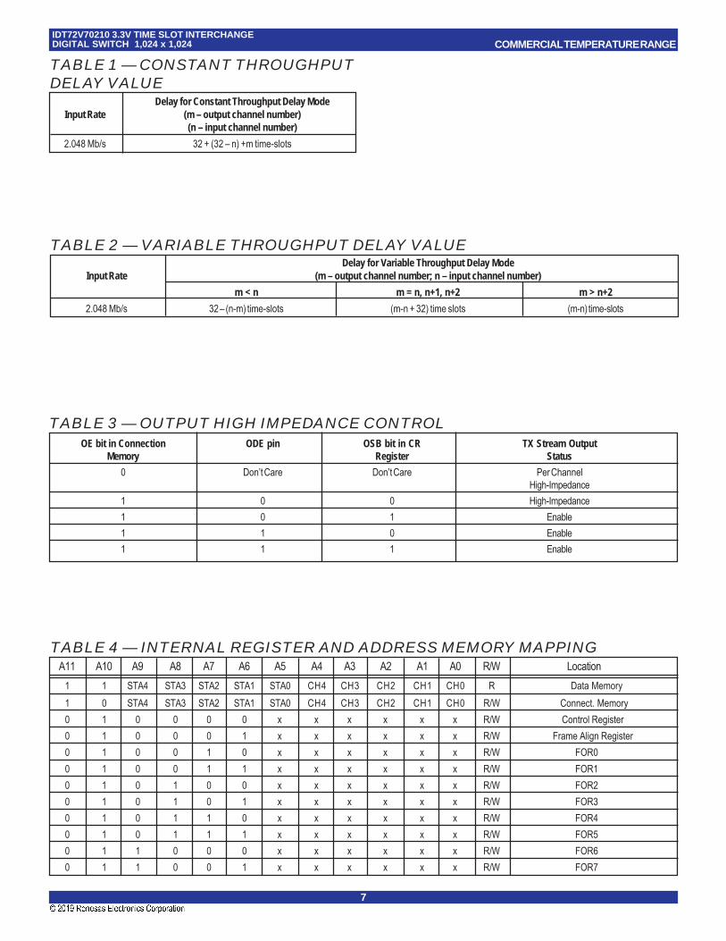
COMMERCIAL TEMPERATURE RANGEIDT72V70210 3.3V TIME SLOT INTERCHANGEDIGITAL SWITCH 1,024 x 1,024
TABLE 1 — CONSTANT THROUGHPUTDELAY VALUE
Delay for Constant Throughput Delay ModeInput Rate (m – output channel number)
(n – input channel number)2.048 Mb/s 32 + (32 – n) +m time-slots
TABLE 2 — VARIABLE THROUGHPUT DELAY VALUEDelay for Variable Throughput Delay Mode
Input Rate (m – output channel number; n – input channel number)m < n m = n, n+1, n+2 m > n+2
2.048 Mb/s 32 – (n-m) time-slots (m-n + 32) time slots (m-n) time-slots
OE bit in Connection ODE pin OSB bit in CR TX Stream OutputMemory Register Status
0 Don’t Care Don’t Care Per ChannelHigh-Impedance
1 0 0 High-Impedance1 0 1 Enable1 1 0 Enable1 1 1 Enable
TABLE 3 — OUTPUT HIGH IMPEDANCE CONTROL
TABLE 4 — INTERNAL REGISTER AND ADDRESS MEMORY MAPPINGA11 A10 A9 A8 A7 A6 A5 A4 A3 A2 A1 A0 R/W Location
1 1 STA4 STA3 STA2 STA1 STA0 CH4 CH3 CH2 CH1 CH0 R Data Memory1 0 STA4 STA3 STA2 STA1 STA0 CH4 CH3 CH2 CH1 CH0 R/W Connect. Memory0 1 0 0 0 0 x x x x x x R/W Control Register0 1 0 0 0 1 x x x x x x R/W Frame Align Register0 1 0 0 1 0 x x x x x x R/W FOR00 1 0 0 1 1 x x x x x x R/W FOR10 1 0 1 0 0 x x x x x x R/W FOR20 1 0 1 0 1 x x x x x x R/W FOR30 1 0 1 1 0 x x x x x x R/W FOR40 1 0 1 1 1 x x x x x x R/W FOR50 1 1 0 0 0 x x x x x x R/W FOR60 1 1 0 0 1 x x x x x x R/W FOR7

8
COMMERCIAL TEMPERATURE RANGEIDT72V70210 3.3V TIME SLOT INTERCHANGEDIGITAL SWITCH 1,024 x 1,024
Reset Value: 0000H.
Bit Name Description15-10 Unused Must be zero for normal operation.
9 MBP When 1, the connection memory block programming feature is ready for the programming of Connection Memory high bits,(Memory Block Program) bit 11 to bit 15. When 0, this feature is disabled.
8-5 BPD4-0 These bits carry the value to be loaded into the connection memory block whenever the memory block programming feature(Block Programming Data) is activated. After the MBP bit in the control register is set to 1 and the BPE bit is set to 1, the contents of the bits BPD3-0 are
loaded into bit 15 and 12 of the connection memory. Bit 11 to bit 0 of the connection memory are set to 0.4 BPE A zero to one transition of this bit enables the memory block programming function. The BPE and BPD4-0 bits in the CR
(Begin Block register have to be defined in the same write operation. Once the BPE bit is set HIGH, the device requires two frames to Programming Enable) complete the block programming. After the programming function has finished, the BPE bit returns to zero to indicate the
operation is completed. When the BPE = 1, the BPE or MBP can be set to 0 to abort to ensure proper operation. WhenBPE = 1, the other bit in the CR register must not be changed for two frames to ensure proper operation.
3 OSB When ODE = 0 and OSB = 0, the output drivers of TX0 to TX31 are in high impedance mode. When ODE = 0 and OSB = 1,(Output Stand By) the output driver of TX0 to TX31 function normally. When ODE = 1, TX0 to TX31 output drivers function normally.
2 SFE A zero to one transition in this bit starts the frame evaluation procedure. When the CFE bit in the FAR register changes from(Start Frame Evaluation) zero to one, the evaluation procedure stops. To start another fame evaluation cycle, set this bit to zero for at least one frame.
1-0 Unused Must be zero for normal operation.
15 14 13 12 11 10 9 8 7 6 5 4 3 2 1 0
0 0 0 0 0 0 MBP BPD3 BPD2 BPD1 BPD0 BPE OSB SFE 0 0
TABLE 5 — CONTROL REGISTER (CR) BITS
TABLE 6 — CONNECTION MEMORY BITS
Bit Name Description15 LPBK When 1, the RX n channel m data comes from the TX n channel m. For proper per channel loopback operations, set the delay
(Per Channel Loopback) offset register bits OFn[2:0] to zero for the streams which are in the loopback mode.14 V/C (Variable/Constant This bit is used to select between the variable (LOW) and constant delay (HIGH) mode on a per-channel basis.
Throughput Delay)13 PC When 1, the contents of the connection memory are output on the corresponding output channel and stream. Only the lower
(Processor Channel) byte (bit 7 – bit 0) will be output to the TX output pins. When 0, the contents of the connection memory are the data memoryaddress of the switched input channel and stream.
12 OE This bit enables the TX output drivers on a per-channel basis. When 1, the output driver functions normally. When 0, the output(Output Enable) driver is in a high-impedance state.
11-7 SAB4-0 (Source Stream The binary value is the number of the data stream for the source of the connection.Address Bits)
6-5 Unused Must be zero for normal operation.4-0 CAB4-0 (Source Channel The binary value is the number of the channel for the source of the connection.
Address Bits)
15 14 13 12 11 10 9 8 7 6 5 4 3 2 1 0
LPBK V/C PC OE SAB4 SAB3 SAB2 SAB1 SAB0 0 0 CAB4 CAB3 CAB2 CAB1 CAB0

9
COMMERCIAL TEMPERATURE RANGEIDT72V70210 3.3V TIME SLOT INTERCHANGEDIGITAL SWITCH 1,024 x 1,024
0 1 2 3 4 5 6 7 8 9 10 11 12 13 14 15 16
ST-BUS® Frame
CLK
Offset Value
FE Input
0 1 2 3 4 5 6 7 8 9 10 11 12 13 14 15
GCI Frame
CLK
Offset Value
FE Input
(FD[10:0] = 06H)(FD11 = 0, sample at CLK LOW phase)
(FD[10:0] = 09H)(FD11 = 1, sample at CLK HIGH phase)
5714 drw 04
Figure 1. Example for Frame Alignment Measurement
Bit Name Description15-13 Unused Must be zero for normal operation
12 CFE (Complete When CFE = 1, the frame evaluation is completed and bits FD10 to FD0 bits contains a valid frame alignment offset. This bit is reset toFrame Evaluation) zero, when SFE bit in the CR register is changed from 1 to 0.
11 FD11 The falling edge of FE (or rising edge for GCI mode) is sampled during the CLK-high phase (FD11 = 1) or during the CLK-low phase(Frame Delay Bit 11) (FD11 = 0). This bit allows the measurement resolution to ½ CLK cycle.
10-0 FD10-0 The binary value expressed in these bits refers to the measured input offset value. These bits are rest to zero when the SFE bit of the(Frame Delay Bits) CR register changes from 1 to 0. (FD10 – MSB, FD0 – LSB)
Reset Value: 0000H.
15 14 13 12 11 10 9 8 7 6 5 4 3 2 1 0
0 0 0 CFE FD11 FD10 FD9 FD8 FD7 FD6 FD5 FD4 FD3 FD2 FD1 FD0
TABLE 7 — FRAME ALIGNMENT REGISTER (FAR) BITS

10
COMMERCIAL TEMPERATURE RANGEIDT72V70210 3.3V TIME SLOT INTERCHANGEDIGITAL SWITCH 1,024 x 1,024
TABLE 8 — FRAME INPUT OFFSET REGISTER (FOR) BITS
Reset Value: 0000H for all FOR registers.
15 14 13 12 11 10 9 8 7 6 5 4 3 2 1 0
OF32 OF31 OF30 DLE3 OF22 OF21 OF20 DLE2 OF12 OF11 OF10 DLE1 OF02 OF01 OF00 DLE0
FOR0 Register15 14 13 12 11 10 9 8 7 6 5 4 3 2 1 0
OF72 OF71 OF70 DLE7 OF62 OF61 OF60 DLE6 OF52 OF51 OF50 DLE5 OF42 OF41 OF40 DLE4
FOR1 Register15 14 13 12 11 10 9 8 7 6 5 4 3 2 1 0
OF112 OF111 OF110 DLE11 OF102 OF101 OF100 DLE10 OF92 OF91 OF90 DLE9 OF82 OF81 OF80 DLE8
FOR2 Register15 14 13 12 11 10 9 8 7 6 5 4 3 2 1 0
OF312 OF311 OF310 DLE31 OF142 OF141 OF140 DLE14 OF132 OF131 OF130 DLE13 OF122 OF121 OF120 DLE12
FOR3 Register15 14 13 12 11 10 9 8 7 6 5 4 3 2 1 0
OF192 OF191 OF190 DLE19 OF182 OF181 OF180 DLE18 OF172 OF171 OF170 DLE17 OD162 OD161 OF160 DLE16
FOR4 Register15 14 13 12 11 10 9 8 7 6 5 4 3 2 1 0
OF232 OF231 OF230 DLE23 OF222 OF221 OF220 DLE22 OF212 OF211 OF210 DLE21 OF202 OF201 OF200 DLE20
FOR5 Register15 14 13 12 11 10 9 8 7 6 5 4 3 2 1 0
OF272 OF271 OF270 DLE27 OF262 OF261 OF260 DLE26 OF252 OF251 OF250 DLE25 OF242 OF241 OF240 DLE24
FOR6 Register15 14 13 12 11 10 9 8 7 6 5 4 3 2 1 0
OF312 OF311 OF310 DLE31 OF302 OF301 OF300 DLE30 OF292 OF291 OF290 DLE29 OF282 OF281 OF280 DLE28
FOR7 Register
Name(1) DescriptionOFn2, OFn1, OFn0 These three bits define how long the serial interface receiver takes to recognize and store bit 0 from the RX input pin: i.e., to start a new frame.(Offset Bits 2, 1 & 0) The input frame offset can be selected to +4.5 clock periods from the point where the external frame pulse input signal is applied to the F0i
input of the device. See Figure 1.DLEn ST-BUS® mode: DLEn = 0, if clock rising edge is at the ¾ point of the bit cell.
(Data Latch Edge) DLEn = 1, if when clock falling edge is at the ¾ of the bit cell.GCI mode: DLEn = 0, if clock falling edge is at the ¾ point of the bit cell.
DLEn = 1, if when clock rising edge is at the ¾ of the bit cell.NOTE:1. n denotes an input stream number from 0 to 31.

11
COMMERCIAL TEMPERATURE RANGEIDT72V70210 3.3V TIME SLOT INTERCHANGEDIGITAL SWITCH 1,024 x 1,024
ST-BUS® F0i
RX Stream
5714 drw 05
Bit 7
Bit 7
CLK
Bit 7
Bit 7
denotes the 3/4 point of the bit cell
offset = 0, DLE = 0
offset = 1, DLE = 0
offset = 0, DLE = 1
offset = 1, DLE = 1
GCI F0i
Bit 0
Bit 0
CLK
Bit 0
Bit 0
denotes the 3/4 point of the bit cell
offset = 0, DLE = 0
offset = 1, DLE = 0
offset = 0, DLE = 1
offset = 1, DLE = 1
RX Stream
RX Stream
RX Stream
RX Stream
RX Stream
RX Stream
RX Stream
Measurement Result from CorrespondingInput Stream Frame Delay Bits Offset Bits
OffsetFD11 FD2 FD1 FD0 OFn2 OFn1 OFn0 DLEn
No clock period shift (Default) 1 0 0 0 0 0 0 0+ 0.5 clock period shift 0 0 0 0 0 0 0 1+ 1.0 clock period shift 1 0 0 1 0 0 1 0+ 1.5 clock period shift 0 0 0 1 0 0 1 1+ 2.0 clock period shift 1 0 1 0 0 1 0 0+ 2.5 clock period shift 0 0 1 0 0 1 0 1+ 3.0 clock period shift 1 0 1 1 0 1 1 0+ 3.5 clock period shift 0 0 1 1 0 1 1 1+ 4.0 clock period shift 1 1 0 0 1 0 0 0+ 4.5 clock period shift 0 1 0 0 1 0 0 1
TABLE 9 — OFFSET BITS (OFn2, OFn1, OFn0, DLEn) & FRAME DELAY BITS(FD11, FD2-0)
Figure 2. Examples for Input Offset Delay Timing

12
COMMERCIAL TEMPERATURE RANGEIDT72V70210 3.3V TIME SLOT INTERCHANGEDIGITAL SWITCH 1,024 x 1,024
JTAG SUPPORTThe IDT72V70210 JTAG interface conforms to the Boundary-Scan stan-
dard IEEE-1149.1. This standard specifies a design-for-testability techniquecalled Boundary-Scan test (BST). The operation of the boundary-scan circuitryis controlled by an external test access port (TAP) Controller.
TEST ACCESS PORT (TAP)The Test Access Port (TAP) provides access to the test functions of the
IDT72V70210. It consists of three input pins and one output pin.•Test Clock Input (TCK)TCK provides the clock for the test logic. The TCK does not interfere
with any on-chip clock and thus remain independent. The TCK permitsshifting of test data into or out of the Boundary-Scan register cellsconcurrently with the operation of the device and without interfering with theon-chip logic.
•Test Mode Select Input (TMS)The logic signals received at the TMS input are interpreted by the TAP
Controller to control the test operations. The TMS signals are sampled at therising edge of the TCK pulse. This pin is internally pulled to VCC when it is notdriven from an external source.
•Test Data Input (TDI)Serial input data applied to this port is fed either into the instruction
register or into a test data register, depending on the sequence previouslyapplied to the TMS input. Both registers are described in a subsequentsection. The received input data is sampled at the rising edge of TCK pulses.This pin is internally pulled to Vcc when it is not driven from an external source.
•Test Data Output (TDO)Depending on the sequence previously applied to the TMS input, the
contents of either the instruction register or data register are serially shifted out
towards the TDO. The data out of the TDO is clocked on the falling edge of theTCK pulses. When no data is shifted through the boundary scan cells, the TDOdriver is set to a high impedance state.
•Test Reset (TRST)Reset the JTAG scan structure. This pin is internally pulled to VCC.
INSTRUCTION REGISTERIn accordance with the IEEE-1149.1 standard, the IDT72V70210 uses
public instructions. The IDT72V70210 JTAG Interface contains a two-bitinstruction register. Instructions are serially loaded into the instruction registerfrom the TDI when the TAP Controller is in its shifted-IR state. Subsequently,the instructions are decoded to achieve two basic functions: to select the test dataregister that may operate while the instruction is current, and to define the serialtest data register path, which is used to shift data between TDI and TDO duringdata register scanning.
TEST DATA REGISTERAs specified in IEEE-1149.1, the IDT72V70210 JTAG Interface contains
two test data registers:•The Boundary-Scan registerThe Boundary-Scan register consists of a series of Boundary-Scan cells
arranged to form a scan path around the boundary of the IDT72V70210 corelogic.
•The Bypass RegisterThe Bypass register is a single stage shift register that provides a one-bit
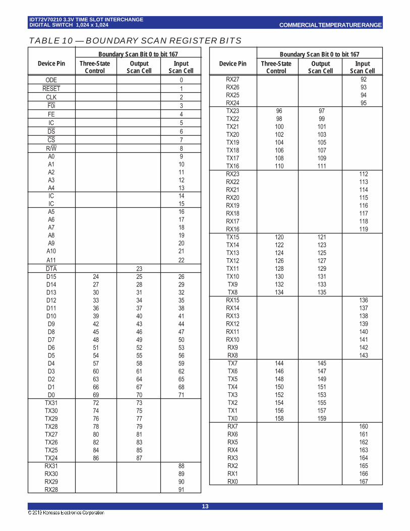
path from TDI to its TDO. The IDT72V70210 boundary scan register bits areshown in Table 10. Bit 0 is the first bit clocked out. All three-state enable bits areactive high.
13
COMMERCIAL TEMPERATURE RANGEIDT72V70210 3.3V TIME SLOT INTERCHANGEDIGITAL SWITCH 1,024 x 1,024
TABLE 10 — BOUNDARY SCAN REGISTER BITS
Boundary Scan Bit 0 to bit 167Device Pin Three-State Output Input
Control Scan Cell Scan CellRX27 92RX26 93RX25 94RX24 95TX23 96 97TX22 98 99TX21 100 101TX20 102 103TX19 104 105TX18 106 107TX17 108 109TX16 110 111RX23 112RX22 113RX21 114RX20 115RX19 116RX18 117RX17 118RX16 119TX15 120 121TX14 122 123TX13 124 125TX12 126 127TX11 128 129TX10 130 131TX9 132 133TX8 134 135
RX15 136RX14 137RX13 138RX12 139RX11 140RX10 141RX9 142RX8 143TX7 144 145TX6 146 147TX5 148 149TX4 150 151TX3 152 153TX2 154 155TX1 156 157TX0 158 159RX7 160RX6 161RX5 162RX4 163RX3 164RX2 165RX1 166RX0 167
Boundary Scan Bit 0 to bit 167Device Pin Three-State Output Input
Control Scan Cell Scan CellODE 0
RESET 1CLK 2F0i 3FE 4IC 5DS 6CS 7
R/W 8A0 9A1 10A2 11A3 12A4 13IC 14IC 15A5 16A6 17A7 18A8 19A9 20
A10 21A11 22DTA 23D15 24 25 26D14 27 28 29D13 30 31 32D12 33 34 35D11 36 37 38D10 39 40 41D9 42 43 44D8 45 46 47D7 48 49 50D6 51 52 53D5 54 55 56D4 57 58 59D3 60 61 62D2 63 64 65D1 66 67 68D0 69 70 71
TX31 72 73TX30 74 75TX29 76 77TX28 78 79TX27 80 81TX26 82 83TX25 84 85TX24 86 87RX31 88RX30 89RX29 90RX28 91

14
COMMERCIAL TEMPERATURE RANGEIDT72V70210 3.3V TIME SLOT INTERCHANGEDIGITAL SWITCH 1,024 x 1,024
Symbol Parameter Min. Typ. Max. UnitsICC (2) Supply Current @ 2 Mb/s - 15 20 mAIIL(3,4) Input Leakage (input pins) - - 50 μAIOZ(3,4) High-impedance Leakage - - 50 μAVOH(5) Output HIGH Voltage 2.4 - - VVOL(6) Output LOW Voltage - - 0.4 V
Symbol Rating Level UnitVTT TTL Threshold 1.5 VVHM TTL Rise/Fall Threshold Voltage HIGH 2.0 VVLM TTL Rise/Fall Threshold Voltage LOW 0.8 V
DC ELECTRICAL CHARACTERISTICS
AC ELECTRICAL CHARACTERISTICS - TIMING PARAMETERMEASUREMENT VOLTAGE LEVELS
NOTES:1. Voltages are with respect to ground (GND) unless otherwise stated.2. Outputs unloaded.3. 0 ≤ V ≤ VCC.4. Maximum leakage on pins (output or I/O pins in high-impedance state) is over an applied voltage (V).5. IOH = 10 mA.6. IOL = 10 mA.
Test Point
OutputPin
CLGND
S1
RL
VCC
GND
5714 drw06
S2
S1 is open circuit except when testing outputlevels or high impedance states.
S2 is switched to VCC or GND when testingoutput levels or high impedance states.
Figure 3. Output Load
Symbol Parameter Min. Max. UnitVCC Supply Voltage 3.0 3.6 VVi Voltage on Digital Inputs GND -0.3 5.3 VIO Current at Digital Outputs -50 50 mATS Storage Temperature -55 +125 °CPD Package Power Dissapation ⎯ 2 W
NOTE:1. Exceeding these values may cause permanent damage. Functional operation underthese conditions is not implied.
ABSOLUTE MAXIMUM RATINGS(1) RECOMMENDED OPERATINGCONDITIONS(1)
NOTE:1.Voltages are with respect to Ground unless otherwise stated.
Symbol Parameter Min. Typ. Max. UnitVCC Positive Supply 3.0 3.3 3.6 VVIH Input HIGH Voltage 2.0 ⎯ 5.3 VVIL Input LOW Voltage ⎯ ⎯ 0.8 VTOP Operating Temperature -40 25 +85 °C
Commercial
15
COMMERCIAL TEMPERATURE RANGEIDT72V70210 3.3V TIME SLOT INTERCHANGEDIGITAL SWITCH 1,024 x 1,024
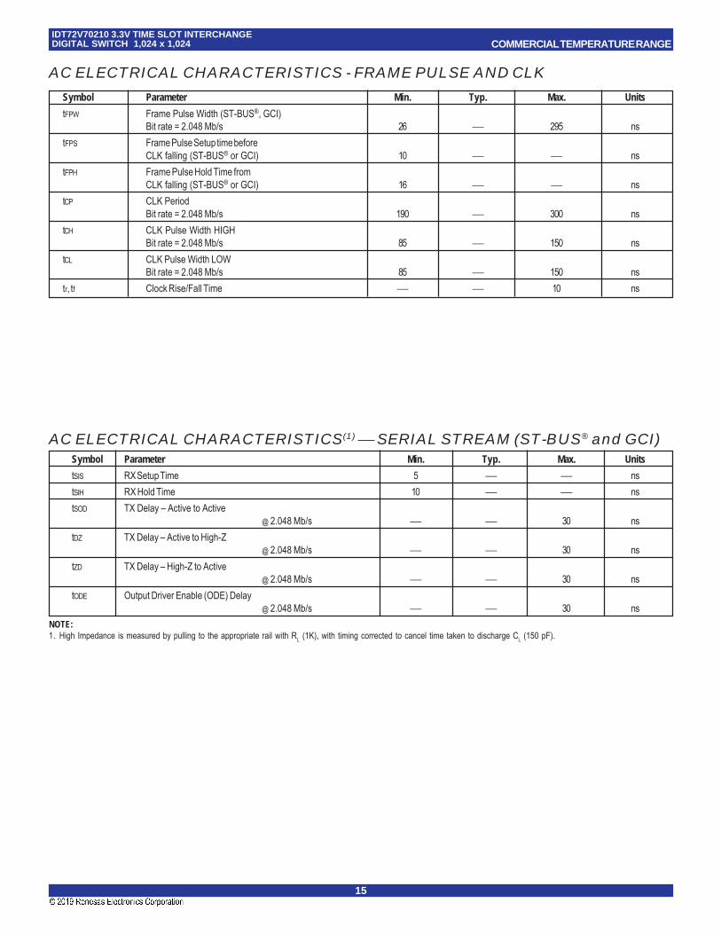
Symbol Parameter Min. Typ. Max. UnitstSIS RX Setup Time 5 ⎯ ⎯ nstSIH RX Hold Time 10 ⎯ ⎯ nstSOD TX Delay – Active to Active
@ 2.048 Mb/s ⎯ ⎯ 30 nstDZ TX Delay – Active to High-Z
@ 2.048 Mb/s ⎯ ⎯ 30 nstZD TX Delay – High-Z to Active
@ 2.048 Mb/s ⎯ ⎯ 30 nstODE Output Driver Enable (ODE) Delay
@ 2.048 Mb/s ⎯ ⎯ 30 ns
AC ELECTRICAL CHARACTERISTICS - FRAME PULSE AND CLK
Symbol Parameter Min. Typ. Max. UnitstFPW Frame Pulse Width (ST-BUS®, GCI)
Bit rate = 2.048 Mb/s 26 ⎯ 295 nstFPS Frame Pulse Setup time before
CLK falling (ST-BUS® or GCI) 10 ⎯ ⎯ nstFPH Frame Pulse Hold Time from
CLK falling (ST-BUS® or GCI) 16 ⎯ ⎯ nstCP CLK Period
Bit rate = 2.048 Mb/s 190 ⎯ 300 nstCH CLK Pulse Width HIGH
Bit rate = 2.048 Mb/s 85 ⎯ 150 nstCL CLK Pulse Width LOW
Bit rate = 2.048 Mb/s 85 ⎯ 150 nstr, tf Clock Rise/Fall Time ⎯ ⎯ 10 ns
AC ELECTRICAL CHARACTERISTICS(1) ⎯ SERIAL STREAM (ST-BUS® and GCI)
NOTE:1. High Impedance is measured by pulling to the appropriate rail with RL (1K), with timing corrected to cancel time taken to discharge CL (150 pF).

16
COMMERCIAL TEMPERATURE RANGEIDT72V70210 3.3V TIME SLOT INTERCHANGEDIGITAL SWITCH 1,024 x 1,024
tFPW
tFPHtFPS
F0i
CLK
TX
RX
tCP
5714 drw 07
Bit 6, Channel 0Bit 7, Channel 0Bit 0, Last Ch(1) Bit 5, Channel 0
Bit 6, Channel 0Bit 7, Channel 0 Bit 5, Channel 0
tCH tCL tr tf
tSIS tSIH
tSOD
Bit 0, Last Ch(1)
Figure 4. ST-BUS® Timing
F0i
CLK
TX
RX
5714 drw 08
Bit 1, Channel 0Bit 0, Channel 0 Bit 2, Channel 0
Bit 1, Channel 0Bit 0, Channel 0 Bit 2, Channel 0Bit 7, Last Ch(1)
Bit 7, Last Ch(1)
tFPHtFPS
tCP
tCH tCL tr tf
tSIS tSIH
tFPW
tSOD
Figure 5. GCI Timing
tDZ
CLK(ST-BUS® mode)
TX
TX VALID DATA
HiZ VALID DATA
HiZ
tZD
CLK(GCI mode)
5714 drw 09
ODE
TX
tODE
VALID DATAHIZ HIZ
5714 drw10
tODE
Figure 6. Serial Output and External Control Figure 7. Output Driver Enable (ODE)
NOTE:1. @ 2.048 Mb/s bit rate, last channel = ch 31,
NOTE:1. @ 2.048 Mb/s, last channel = ch 31,
17
COMMERCIAL TEMPERATURE RANGEIDT72V70210 3.3V TIME SLOT INTERCHANGEDIGITAL SWITCH 1,024 x 1,024
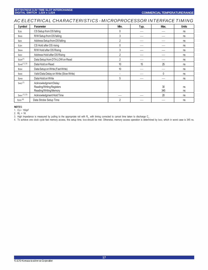
AC ELECTRICAL CHARACTERISTICS - MICROPROCESSOR INTERFACE TIMING
NOTES:1. CL= 150pF2. RL = 1K3. High Impedance is measured by pulling to the appropriate rail with RL, with timing corrected to cancel time taken to discharge CL.4. To achieve one clock cycle fast memory access, this setup time, tDSS should be met. Otherwise, memory access operation is determined by tAKD, which in worst case is 345 ns.
Symbol Parameter Min. Typ. Max. UnitstCSS CS Setup from DS falling 0 ⎯ ⎯ nstRWS R/W Setup from DS falling 3 ⎯ ⎯ nstADS Address Setup from DS falling 2 ⎯ ⎯ nstCSH CS Hold after DS rising 0 ⎯ ⎯ nstRWH R/W Hold after DS Rising 3 ⎯ ⎯ nstADH Address Hold after DS Rising 2 ⎯ ⎯ nstDDR(1) Data Setup from DTA LOW on Read 2 ⎯ ⎯ nstDHR(1,2,3) Data Hold on Read 10 15 25 nstDSW Data Setup on Write (Fast Write) 10 ⎯ ⎯ nstSWD Valid Data Delay on Write (Slow Write) - ⎯ 0 nstDHW Data Hold on Write 5 ⎯ ⎯ nstAKD (1) Acknowledgment Delay:
Reading/Writing Registers 30 nsReading/Writing Memory 345 ns
tAKH (1,2,3) Acknowledgment Hold Time ⎯ ⎯ 20 ns tDSS (4) Data Strobe Setup Time 2 ⎯ ⎯ ns

18
COMMERCIAL TEMPERATURE RANGEIDT72V70210 3.3V TIME SLOT INTERCHANGEDIGITAL SWITCH 1,024 x 1,024
DS
5714 drw 11
VALID WRITE DATA
D0-D15READ
CS
DTA
VALID READ DATA
VALID ADDRESS
tAKH
D0-D15WRITE
R/W
A0-A11
CLK GCI
CLK ST-BUS®
tDDR
tAKD
tSWD
tADS
tDSW tDHW
tDHR
tADH
tRWHtRWS
tDSS
tCSH
tCSS
Figure 8. Motorola Non-Mulitplexed Bus Timing
19
CORPORATE HEADQUARTERS for SALES: for Tech Support:2975 Stender Way 800-345-7015 or 408-727-6116 408-330-1552Santa Clara, CA 95054 fax: 408-492-8649 email: [email protected]
www.idt.com
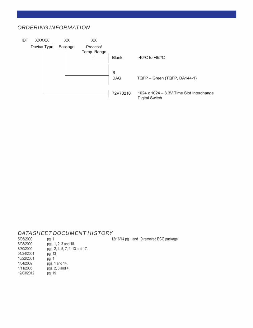
ORDERING INFORMATION
DATASHEET DOCUMENT HISTORY5/05/2000 pg. 1 12/16/14 pg 1 and 19 removed BCG package6/08/2000 pgs. 1, 2, 3 and 18.8/30/2000 pgs. 2, 4, 5, 7, 9, 13 and 17.01/24/2001 pg. 1310/22/2001 pg. 11/04/2002 pgs. 1 and 14.1/11/2005 pgs. 2, 3 and 4.12/03/2012 pg. 19
IDT XXXXX XX XXDevice Type Package
DAG TQFP – Green (TQFP, DA144-1)
1024 x 1024 – 3.3V Time Slot Interchange Digital Switch
-40ºC to +85ºC
72V70210
Process/Temp. Range
Blank
B
rdvorak
Rectangle

Corporate HeadquartersTOYOSU FORESIA, 3-2-24 Toyosu,Koto-ku, Tokyo 135-0061, Japanwww.renesas.com
Contact InformationFor further information on a product, technology, the most up-to-date version of a document, or your nearest sales office, please visit:www.renesas.com/contact/
TrademarksRenesas and the Renesas logo are trademarks of Renesas Electronics Corporation. All trademarks and registered trademarks are the property of their respective owners.
IMPORTANT NOTICE AND DISCLAIMER
RENESAS ELECTRONICS CORPORATION AND ITS SUBSIDIARIES (“RENESAS”) PROVIDES TECHNICAL SPECIFICATIONS AND RELIABILITY DATA (INCLUDING DATASHEETS), DESIGN RESOURCES (INCLUDING REFERENCE DESIGNS), APPLICATION OR OTHER DESIGN ADVICE, WEB TOOLS, SAFETY INFORMATION, AND OTHER RESOURCES “AS IS” AND WITH ALL FAULTS, AND DISCLAIMS ALL WARRANTIES, EXPRESS OR IMPLIED, INCLUDING, WITHOUT LIMITATION, ANY IMPLIED WARRANTIES OF MERCHANTABILITY, FITNESS FOR A PARTICULAR PURPOSE, OR NON-INFRINGEMENT OF THIRD PARTY INTELLECTUAL PROPERTY RIGHTS.
These resources are intended for developers skilled in the art designing with Renesas products. You are solely responsible for (1) selecting the appropriate products for your application, (2) designing, validating, and testing your application, and (3) ensuring your application meets applicable standards, and any other safety, security, or other requirements. These resources are subject to change without notice. Renesas grants you permission to use these resources only for development of an application that uses Renesas products. Other reproduction or use of these resources is strictly prohibited. No license is granted to any other Renesas intellectual property or to any third party intellectual property. Renesas disclaims responsibility for, and you will fully indemnify Renesas and its representatives against, any claims, damages, costs, losses, or liabilities arising out of your use of these resources. Renesas' products are provided only subject to Renesas' Terms and Conditions of Sale or other applicable terms agreed to in writing. No use of any Renesas resources expands or otherwise alters any applicable warranties or warranty disclaimers for these products.
(Rev.1.0 Mar 2020)
© 2020 Renesas Electronics Corporation. All rights reserved.