3.3 V powered, 15 kV ESD protected, up to 12 Mbps RS-485/RS … · October 2017 DocID9102 Rev 11...
24
October 2017 DocID9102 Rev 11 1/24 This is information on a product in full production. www.st.com ST3485EB, ST3485EC, ST3485EI, ST3485EIY 3.3 V powered, 15 kV ESD protected, up to 12 Mbps RS-485/ RS-422 transceiver Datasheet - production data Features ESD protection ±15 kV IEC 61000-4-2 air discharge ±8 kV IEC 61000-4-2 contact discharge Operate from a single 3.3 V supply - no charge pump required Interoperable with 5 V logic 1 μA low current shutdown mode max. Guaranteed 12 Mbps data rate -7 to 12 V common mode input voltage range Half duplex versions available Industry standard 75176 pinout Current limiting and thermal shutdown for driver overload protection Guaranteed high receiver output state for floating inputs with no signal present Allow up to 64 transceivers on the bus Available in SO8 package Automotive grade (ST3485EIY) Description The ST3485EB/EC/EI/EIY device is ±15 kV ESD protected, 3.3 V low power transceiver for RS- 485 and RS-422 communications. The device contains one driver and one receiver in half duplex configuration. The ST3485E device transmits and receives at a guaranteed data rate of at least 12 Mbps. All transmitter outputs and receiver inputs are protected to ±15 kV IEC 61000-4-2 air discharge. The driver is short-circuit current limited and is protected against excessive power dissipation by thermal shutdown circuitry that places the driver outputs into a high impedance state. Table 1: Device summary Order code Temp. range Package Packing ST3485ECDR 0 to 70 °C SO8 (tape and reel) 2500 parts per reel ST3485EBDR -40 to 85 °C ST3485EIDT -40 to 125 °C ST3485EIYDT
-
Upload
doannguyet -
Category
Documents
-
view
213 -
download
0
Transcript of 3.3 V powered, 15 kV ESD protected, up to 12 Mbps RS-485/RS … · October 2017 DocID9102 Rev 11...

October 2017 DocID9102 Rev 11 1/24
This is information on a product in full production. www.st.com
ST3485EB, ST3485EC, ST3485EI, ST3485EIY
3.3 V powered, 15 kV ESD protected, up to 12 Mbps RS-485/ RS-422 transceiver
Datasheet - production data
Features ESD protection
±15 kV IEC 61000-4-2 air discharge
±8 kV IEC 61000-4-2 contact discharge
Operate from a single 3.3 V supply - no charge pump required
Interoperable with 5 V logic
1 µA low current shutdown mode max.
Guaranteed 12 Mbps data rate
-7 to 12 V common mode input voltage range
Half duplex versions available
Industry standard 75176 pinout
Current limiting and thermal shutdown for driver overload protection
Guaranteed high receiver output state for floating inputs with no signal present
Allow up to 64 transceivers on the bus
Available in SO8 package
Automotive grade (ST3485EIY)
Description The ST3485EB/EC/EI/EIY device is ±15 kV ESD protected, 3.3 V low power transceiver for RS-485 and RS-422 communications. The device contains one driver and one receiver in half duplex configuration.
The ST3485E device transmits and receives at a guaranteed data rate of at least 12 Mbps.
All transmitter outputs and receiver inputs are protected to ±15 kV IEC 61000-4-2 air discharge.
The driver is short-circuit current limited and is protected against excessive power dissipation by thermal shutdown circuitry that places the driver outputs into a high impedance state.
Table 1: Device summary
Order code Temp. range Package Packing
ST3485ECDR 0 to 70 °C
SO8 (tape and reel) 2500 parts per reel ST3485EBDR -40 to 85 °C
ST3485EIDT -40 to 125 °C
ST3485EIYDT

Contents ST3485EB, ST3485EC, ST3485EI, ST3485EIY
2/24 DocID9102 Rev 11
Contents
1 Pin configuration ............................................................................. 3
2 Truth tables ...................................................................................... 4
3 Maximum ratings ............................................................................. 5
4 Electrical characteristics ................................................................ 6
5 Test circuits and typical characteristics ...................................... 10
6 Package information ..................................................................... 19
6.1 SO8 package information ................................................................ 19
6.2 SO8 tape and reel information ........................................................ 20
7 Ordering information ..................................................................... 21
8 Revision history ............................................................................ 22

ST3485EB, ST3485EC, ST3485EI, ST3485EIY Pin configuration
DocID9102 Rev 11 3/24
1 Pin configuration Figure 1: Pin connections
Table 2: Pin description
Pin n° Symbol Name and function
1 RO Receiver output. If A > B by 200 mV, RO will be high; if A < B by 200
mV, RO will be low.
2 RE
Receiver output enable. RO is enabled when RE is low; RO is high
impedance when RE is high. If RE is high and DE is low, the
device will enter a low power shutdown mode.
3 DE
Driver output enable. The driver outputs are enabled by bringing DE
high. They are high impedance when DE is low. If RE is high DE is
low, the device will enter a low-power shutdown mode. If the driver
outputs are enabled, the part functions as line driver, while they are
high impedance, it functions as line receivers if RE is low.
4 DI Driver input. A low on DI forces output A low and output B high.
Similarly, a high on DI forces output A high and output B low.
5 GND Ground.
6 A Non-inverting receiver input and non-inverting driver output.
7 B Inverting receiver input and inverting driver output.
8 VCC Supply voltage: VCC = 3 V to 3.6 V.
RO
RE
DE
DI
VCC
GND
B
A
1
2
3
4
8
7
6
5

Truth tables ST3485EB, ST3485EC, ST3485EI, ST3485EIY
4/24 DocID9102 Rev 11
2 Truth tables Table 3: Truth table (driver)
Inputs Outputs
Mode RE DE DI B A
X H H L H
Normal L H L
L L X Z Z
H Shutdown
Note: X = “don’t care”; Z = high impedance
Table 4: Truth table (receiver)
Inputs Output
Mode RE DE A-B RO
L L
≥ 0.2 V H
Normal ≤ -0.2 V L
Inputs open H
H X Z Shutdown
Note: X = “don’t care”; Z = high impedance

ST3485EB, ST3485EC, ST3485EI, ST3485EIY Maximum ratings
DocID9102 Rev 11 5/24
3 Maximum ratings
Absolute maximum ratings are those values beyond which damage to the device may occur. Functional operation under these condition is not implied.
Table 5: Absolute maximum ratings
Symbol Parameter Value Unit
VCC Supply voltage 7
V
VI Control input voltage ( RE , DE) -0.3 to 7
VDI Driver input voltage (DI) -0.3 to 7
VDO Driver output voltage (A, B) ±14
VRI Receiver input voltage (A, B) ±14
VRO Receiver output voltage (RO) -0.3 to (VCC + 0.3)
ESD
HBM: human body model for the line inputs
(A and B) (1) 12
kV
HBM: human body model for the logic
inputs (DI, DE, RE ) (1) 4
HBM: human body model for all other pins (1)
2
CDM: charged device model (2) 1.5
Notes:
(1)Human body model: 100 pF discharged through a 1.5 kΩ resistor between two pins of the device, done for all couples of pin combinations with other pins floating. (2)Charged device model: all pins plus package are charged together to the specified voltage and then discharged directly to ground.

Electrical characteristics ST3485EB, ST3485EC, ST3485EI, ST3485EIY
6/24 DocID9102 Rev 11
4 Electrical characteristics Table 6: Electrical characteristics (VCC = 3 V to 3.6 V, TA = 0 to 70 °C for ST3485ECDR, TA = -
40 to 85 °C for ST3485EBDR, TA = -40 to 125 °C for ST3485EIDT and ST3485EIYDT, unless otherwise specified. Typical values are referred to TA = 25 °C)
Symbol Parameter Test conditions Min. Typ. Max. Unit
ISUPPLY VCC power supply current No load, DI = 0 V or VCC
DE = VCC,
RE = 0 V
or VCC
—
1.3 2.2
mA
DE = 0 V,
RE = 0 V 1.2 1.9
ISHDN Shutdown supply current DE = 0 V, RE = VCC, DI = 0 V or VCC 0.002 1 µA
Table 7: Logic input electrical characteristics (VCC = 3 V to 3.6 V, TA = 0 to 70 °C for ST3485ECDR, TA = -40 to 85 °C for ST3485EBDR, TA = -40 to 125 °C for ST3485EIDT and
ST3485EIYDT, unless otherwise specified. Typical values are referred to TA = 25 °C)
Symbol Parameter Test conditions Min. Typ. Max. Unit
VIL Input logic threshold low DE, DI, RE
1.3 0.8
V
VIH Input logic threshold high DE, DI, RE 2
IIN1 Logic input current DE, DI, RE
±2.0 µA
IIN2 Input current (A, B) DE = 0 V, VCC= 0 or 3.6 V VIN = 12 V
1
mA VIN = -7 V
-0.8

ST3485EB, ST3485EC, ST3485EI, ST3485EIY Electrical characteristics
DocID9102 Rev 11 7/24
Table 8: Transmitter electrical characteristics (VCC = 3 V to 3.6 V, TA = 0 to 70 °C for ST3485ECDR, TA = -40 to 85 °C for ST3485EBDR, TA = -40 to 125 °C for ST3485EIDT and
ST3485EIYDT, unless otherwise specified. Typical values are referred to TA = 25 °C)
Symbol Parameter Test conditions Min. Typ. Max. Unit
VOD Differential drive output
RL= 100 Ω (RS-422) (Figure 2) 2
—
V
RL= 54 Ω (RS-485) (Figure 2) 1.5
RL= 60 Ω (RS-485) (Figure 3) 1.5
∆VOD
Change in magnitude of
driver differential output
voltage for
complementary output
states (1)
RL= 54 Ω or 100 Ω (Figure 2)
0.2
VOC Driver common mode
output voltage RL= 54 Ω or 100 Ω (Figure 2)
3
∆VOC
Change in magnitude of
driver common mode
output voltage(1)
RL= 54 Ω or 100 Ω (Figure 2)
0.2
IOSD Driver short-circuit output
current ±250 mA
Notes:
(1)∆VOD and ∆VOC are the changes in VOD and VOC, respectively, when the DI input changes state.
Table 9: Receiver electrical characteristics (VCC = 3 V to 3.6 V, TA = 0 to 70 °C for ST3485ECDR, TA = -40 to 85 °C for ST3485EBDR, TA = -40 to 125 °C for ST3485EIDT and
ST3485EIYDT, unless otherwise specified. Typical values are referred to TA = 25 °C)
Symbol Parameter Test conditions Min. Typ. Max. Unit
VTH Receiver differential
threshold voltage VCM = -7 V to 12 V, DE = 0 -0.2
0.2 V
∆VTH Receiver input hysteresis VCM = 0 V
70
mV
VOH Receiver output high
voltage IOUT = -4 mA, VID = 200 mV (Figure 4) 2
V
VOL Receiver output low
voltage IOUT = 4 mA, VID = -200 mV (Figure 4)
0.4
IOZR 3-state (high impedance)
output current at receiver VCC = 3.6 V, VO = 0 V to VCC
±1 µA
RRIN Receiver input resistance VCM = -7 V to 12 V 24
kΩ
IOSR Receiver short-circuit
current VRO = 0 V to VCC 7
60 mA

Electrical characteristics ST3485EB, ST3485EC, ST3485EI, ST3485EIY
8/24 DocID9102 Rev 11
Table 10: Driver switching characteristics (VCC = 3 V to 3.6 V, TA = 0 to 70 °C for ST3485ECDR, TA = -40 to 85 °C for ST3485EBDR, TA = -40 to 125 °C for ST3485EIDT and
ST3485EIYDT, unless otherwise specified. Typical values are referred to TA = 25 °C)
Symbol Parameter Test conditions Min. Typ. Max. Unit
DR Maximum data rate
12 15
Mbps
tDD Differential output delay RL= 60 Ω, CL = 15 pF (Figure 5 and
Figure 6) 18 30
ns
tTD Differential output
transition time
RL= 60 Ω, CL = 15 pF (Figure 5 and
Figure 6) 12 20
tPLH tPHL Propagation delay RL= 27 Ω, CL = 15 pF (Figure 9 and
Figure 10) 18 30
tPDS
|tPLH - tPHL| driver
propagation delay skew (1)
RL= 27 Ω, CL = 15 pF (Figure 9 and
Figure 10) 2 5
tPZL Output enable time RL= 110 Ω (Figure 11 and Figure 12)
19 35
tPZH Output enable time RL= 110 Ω (Figure 7 and Figure 8)
30 50
tPHZ Output disable time RL= 110 Ω (Figure 7 and Figure 8)
19 35
tPLZ Output disable time RL= 110 Ω (Figure 11 and Figure 12)
30 50
tSKEW Differential output delay
skew 1 3
tPSH Driver enable from
shutdown to output high RL = 110 Ω (Figure 7 and Figure 8)
30 50
tPSL Driver enable from
shutdown to output low RL = 110 Ω (Figure 11 and Figure 12)
19 35
Notes:
(1)Measured on |tPLH(A)-tPHL(A)| and |tPLH(B)-tPHL(B)|.
ST3485EB, ST3485EC, ST3485EI, ST3485EIY Electrical characteristics
DocID9102 Rev 11 9/24
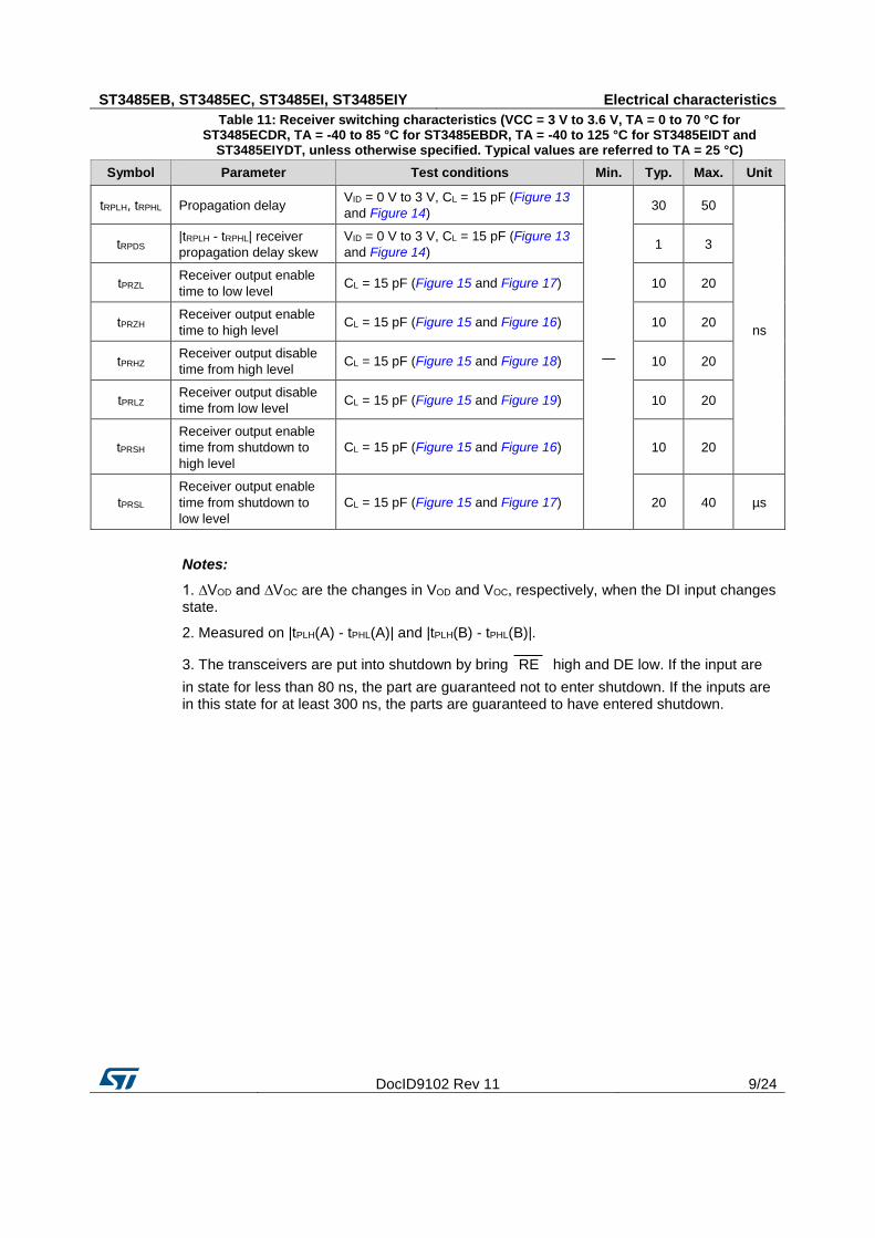
Table 11: Receiver switching characteristics (VCC = 3 V to 3.6 V, TA = 0 to 70 °C for ST3485ECDR, TA = -40 to 85 °C for ST3485EBDR, TA = -40 to 125 °C for ST3485EIDT and
ST3485EIYDT, unless otherwise specified. Typical values are referred to TA = 25 °C)
Symbol Parameter Test conditions Min. Typ. Max. Unit
tRPLH, tRPHL Propagation delay VID = 0 V to 3 V, CL = 15 pF (Figure 13
and Figure 14)
—
30 50
ns
tRPDS |tRPLH - tRPHL| receiver
propagation delay skew
VID = 0 V to 3 V, CL = 15 pF (Figure 13
and Figure 14) 1 3
tPRZL Receiver output enable
time to low level CL = 15 pF (Figure 15 and Figure 17) 10 20
tPRZH Receiver output enable
time to high level CL = 15 pF (Figure 15 and Figure 16) 10 20
tPRHZ Receiver output disable
time from high level CL = 15 pF (Figure 15 and Figure 18) 10 20
tPRLZ Receiver output disable
time from low level CL = 15 pF (Figure 15 and Figure 19) 10 20
tPRSH
Receiver output enable
time from shutdown to
high level
CL = 15 pF (Figure 15 and Figure 16) 10 20
tPRSL
Receiver output enable
time from shutdown to
low level
CL = 15 pF (Figure 15 and Figure 17) 20 40 µs
Notes:
1. ∆VOD and ∆VOC are the changes in VOD and VOC, respectively, when the DI input changes state.
2. Measured on |tPLH(A) - tPHL(A)| and |tPLH(B) - tPHL(B)|.
3. The transceivers are put into shutdown by bring RE high and DE low. If the input are
in state for less than 80 ns, the part are guaranteed not to enter shutdown. If the inputs are in this state for at least 300 ns, the parts are guaranteed to have entered shutdown.

Test circuits and typical characteristics ST3485EB, ST3485EC, ST3485EI, ST3485EIY
10/24 DocID9102 Rev 11
5 Test circuits and typical characteristics
Figure 2: Driver and VOC test load
Figure 3: Driver VOD with varying common mode voltage test load
Figure 4: Receiver VOH and VOL test circuit
D
VCC
VOD
VOC
RL
2
RL
2
375 Ω
375 Ω
RLVOD
VCC
DVCM = -7 to 12 V
VID
0 V
R
VOL IOL (+) VOH IOL (-)

ST3485EB, ST3485EC, ST3485EI, ST3485EIY Test circuits and typical characteristics
DocID9102 Rev 11 11/24
Figure 5: Drive differential output delay transition time test circuit
1. The input pulse is supplied by a generator with the following characteristics: PRR = 250 kHz, 50 % duty cycle, tr ≤ 6.0 ns, ZO = 50 Ω.
2. CL includes probe and stray capacitance
Figure 6: Drive differential output delay transition time waveform
Figure 7: Drive enable and disable times test circuit (pull-down configuration)
1. The input pulse is supplied by a generator with the following characteristics: PRR = 250 kHz, 50 % duty cycle, tr ≤ 6.0 ns.
2. CL includes probe and stray capacitance
IN(1)
D
VCC
CL
RL = 60 Ω
CL = 15 pF(2)
OUT
IN
OUT
1.5 V
tDOtDD
3 V
0 V
2 V
-2 V
50 %
10 %
90 %
t TD
1.5 V
t TD
50 %
10 %
90 %
0 V or 3 V
IN(1)
D
S1
CL = 50 pF(2)
RL = 110 Ω
OUT

Test circuits and typical characteristics ST3485EB, ST3485EC, ST3485EI, ST3485EIY
12/24 DocID9102 Rev 11
Figure 8: Drive enable and disable times waveforms (pull-down configuration)
1. tPZH is valid if the driver is initially disabled ( RE is high), tPSH is valid if the driver is
initially in shutdown mode (RE is low).
Figure 9: Drive propagation time test circuit
1. The input pulse is supplied by a generator with the following characteristics: PRR = 250 kHz, 50 % duty cycle, tr ≤ 6.0 ns.
2. CL includes probe and stray capacitance
IN
OUT
tPZH or tPSH(1)
1.5 V 1.5 V
VOM
tPHZ
3 V
0 V
VOH0.25 V
0 V
IN(1)
VCC
D
S1
VOM = (VOH = VOL)/2 = 1.5 V
RL = 27 Ω
OUT
CL = 15 pF(2)

ST3485EB, ST3485EC, ST3485EI, ST3485EIY Test circuits and typical characteristics
DocID9102 Rev 11 13/24
Figure 10: Drive propagation time waveform
Figure 11: Drive enable and disable times test circuit (pull-up configuration)
1. The input pulse is supplied by a generator with the following characteristics: PRR = 250 kHz, 50 % duty cycle, tr ≤ 6.0 ns.
2. CL includes probe and stray capacitance
IN
OUT A
OUT B
1.5 V 1.5 V
3 V
0 V
t PHLt PLH
VOM VOM
t PHL t PLH
VOM VOM
VOH
VOL
VOH
VOL
VCC
RL = 110 Ω
OUT
CL = 50 pF(2)
S1
D0 V or 3 V
IN(1)

Test circuits and typical characteristics ST3485EB, ST3485EC, ST3485EI, ST3485EIY
14/24 DocID9102 Rev 11
Figure 12: Drive enable and disable times waveforms (pull-up configuration)
1. tPZL is valid if the driver is initially disabled ( RE is high), tPSL is valid if the driver is
initially in shutdown mode (RE is low).
Figure 13: Receiver propagation delay time test circuit
1. The input pulse is supplied by a generator with the following characteristics: PRR = 250 kHz, 50 % duty cycle, tr ≤ 6.0 ns.
2. CL includes probe and stray capacitance
IN
OUT
tPZL or tPSL(1)
VOM
1.5 V 1.5 V
t PLZ
0.25 V
3 V
0 V
VCC
VOL
IN(1)
VID ROUT
CL = 1.5 pF(2)
1.5 V
0 V

ST3485EB, ST3485EC, ST3485EI, ST3485EIY Test circuits and typical characteristics
DocID9102 Rev 11 15/24
Figure 14: Receiver propagation delay time waveforms
Figure 15: Receiver enable and disable times test circuit
1. The input pulse is supplied by a generator with the following characteristics: PRR = 250 kHz, 50 % duty cycle, tr ≤ 6.0 ns.
2. CL includes probe and stray capacitance
IN
OUT
1.5 V 1.5 V
t RPLH t RPHL
VOM
VOM = VCC/2
VOM
3.0 V
0 V
VCC
0 V
1.5 V
-1.5 V
IN(1)
S3
VID R
OUT
CL(2)
1 kΩ
S1
S2
VCC

Test circuits and typical characteristics ST3485EB, ST3485EC, ST3485EI, ST3485EIY
16/24 DocID9102 Rev 11
Figure 16: Receiver enable and disable times waveform (test 1)
Figure 17: Receiver enable and disable times waveform (test 2)
Figure 18: Receiver enable and disable times waveform (test 3)
IN
OUT
1.5 V
t PRZHt PRSH
1.5 V
S1 open
S2 closed
S3 = 1.5 V
3 V
0 V
VOH
0 V
IN
OUT
1.5 V
S1 closed
S2 open
S3 = -1.5 V
t PRZLt PRSL
1.5 V
3 V
0 V
VCC
VOL
IN
OUT
1.5 V
t PRHZ
VOH - 0.25 V
S1 open
S2 closedS3 = 1.5 V
3 V
0 V
VOH
0 V

ST3485EB, ST3485EC, ST3485EI, ST3485EIY Test circuits and typical characteristics
DocID9102 Rev 11 17/24
Figure 19: Receiver enable and disable times waveform (test 4)
Figure 20: Receiver output current vs. output low
voltage
Figure 21: Receiver output current vs. output high
voltage
Figure 22: Low level driver output capability
Figure 23: High level driver output capability
IN
OUT
1.5 V
t PRLZ
0.25 V
S1 closed
S2 open
S3 = -1.5 V
3 V
0 V
VCC
VOL

Test circuits and typical characteristics ST3485EB, ST3485EC, ST3485EI, ST3485EIY
18/24 DocID9102 Rev 11
Figure 24: Receiver input characteristics
Figure 25: Driver short-circuit current (test 1)
Figure 26: Driver short-circuit current (test 2)

ST3485EB, ST3485EC, ST3485EI, ST3485EIY Package information
DocID9102 Rev 11 19/24
6 Package information
In order to meet environmental requirements, ST offers these devices in different grades of ECOPACK® packages, depending on their level of environmental compliance. ECOPACK® specifications, grade definitions and product status are available at: www.st.com. ECOPACK® is an ST trademark.
6.1 SO8 package information
Figure 27: SO8 package outline
Table 12: SO8 mechanical data
Ref.
Dimensions
Millimeters Inches
Min. Typ. Max. Min. Typ. Max
A
1.75
0.069
A1 0.10
0.25 0.004
0.010
A2 1.25
0.049
b 0.28
0.48 0.011
0.019
c 0.17
0.23 0.007
0.010
D 4.80 4.90 5.00 0.189 0.193 0.197
E 5.80 6.00 6.20 0.228 0.236 0.244
E1 3.80 3.90 4.00 0.150 0.154 0.157
e
1.27
0.050
h 0.25
0.50 0.010
0.020
L 0.40
1.27 0.016
0.050
L1
1.04
0.040
k 0°
8° 0°
8°
ccc
0.10
0.004

Package information ST3485EB, ST3485EC, ST3485EI, ST3485EIY
20/24 DocID9102 Rev 11
6.2 SO8 tape and reel information
Figure 28: SO8 tape and reel outline
1. Drawing not to scale
Table 13: SO8 tape and reel mechanical data
Symbol
Dimensions
mm Inches
Min. Typ. Max. Min. Typ. Max.
A
—
330
—
12.992
C 12.8 13.2 0.504 0.519
D 20.2
0.795
N 60
2.362
T
22.4
0.882
Ao 8.1 8.5 0.319 0.335
Bo 5.5 5.9 0.216 0.232
Ko 2.1 2.3 0.082 0.090
Po 3.9 4.1 0.153 0.161
P 7.9 8.1 0.311 0.319

ST3485EB, ST3485EC, ST3485EI, ST3485EIY Ordering information
DocID9102 Rev 11 21/24
7 Ordering information Table 14: Order codes
Order code Temperature range Package Packaging Marking
ST3485ECDR 0 to 70 °C
SO8 Tape and reel
3485EC
ST3485EBDR -40 to 85 °C 3485EB
ST3485EIDT -40 to 125 °C 3485EI
ST3485EIYDT(1) -40 to 125 °C (automotive grade) 3485EIY
Notes:
(1)Qualification and characterization according to AEC Q100 and Q003 or equivalent, advanced screening according to AEC Q001 and Q 002 or equivalent.

Revision history ST3485EB, ST3485EC, ST3485EI, ST3485EIY
22/24 DocID9102 Rev 11
8 Revision history Table 15: Document revision history
Date Revision Changes
20-Jun-2005 2 Mistake on table 12 tZL(SHDN) ms ==> µs.
30-Aug-2005 3 Remove (TRUE) on title, description has been updated in cover page. The
VTH and DVTH values are changed in table 10.
07-Apr-2006 4 Order codes updated.
12-Nov-2007 5 Added Table 1.
18-Dec-2013 6
Updated Features (added SO-8 package, replaced human body model by
±15 kV IEC 61000-4-2 air discharge and IEC 1000-4-2 by IEC 61000-4-2).
Updated Description (renamed device to ST3485EB/EC, replaced human
body model by ±15 kV IEC 61000-4-2 air discharge).
Removed ST3485ECN device from Table 1.
Updated title of Table 6, cross-references, replaced human body model
(HBM) by ±15 kV IEC 61000-4-2 air discharge and IEC 1000-4-2 by IEC
61000-4-2.
Added notes below Table 9.
Updated Table 10 to Table 12 (updated data, cross-references).
Updated Figure 5 to Figure 16 (updated data, added notes below figures and
highlighted some parts of Figure 6 and Figure 12).
Removed DIP-8 package from Section 6: "Package information" and whole
document. Reformatted Section 6: "Package information" (added Figure 27,
Figure 28, Table 13 and Table 14, reversed order of figures and table).
Minor corrections throughout document.
12-Jun-2015 7
Added part number ST3485EIY
Added order code ST3485EIYDT and pointed out in Features it is automotive grade.
Table 7 and Table 9 through to Table 12: replaced TA = -40 to 85 °C with TA = 0 to 70 °C (ST3485ECDR), TA = -40 to 85 °C (ST3485EBDR), and TA = -40 to 125 °C (ST3485EIYDT).
Updated titles of figures 7, 8, 11, 12, 16, 17, 18, 19, 25, and 26
15-Mar-2016 8
Table 5: added ESD information
Removed "Table 6: ESD performance: transmitter outputs, receiver inputs (A, B)".
Added Section 7: "Ordering information"
02-Aug-2016 9
Added new part number ST3485EI
Table 1: "Device summary": added information for new part number ST3485EI.
Removed "Note" icons throughout datasheet
Section 4: "Electrical characteristics": updated TA information
Section 5: "Test circuits and typical characteristics": removed overline bar concerning "RE is low" in note 1 of figures 8 and 12.
Table 14: "Order codes": added ST3485EIDT and updated footnote 1 (ST3485EIYDT now qualified).
25-Aug-2016 10 Table 14: "Order codes": updated order codes ST3485EBDR and ST3485ECDR.

ST3485EB, ST3485EC, ST3485EI, ST3485EIY Revision history
DocID9102 Rev 11 23/24
Date Revision Changes
26-Oct-2017 11
Updated Figure 20: "Receiver output current vs. output low voltage", Figure 21: "Receiver output current vs. output high voltage", Figure 24: "Receiver input characteristics" and Figure 26: "Driver short-circuit current (test 2)".

ST3485EB, ST3485EC, ST3485EI, ST3485EIY
24/24 DocID9102 Rev 11
IMPORTANT NOTICE – PLEASE READ CAREFULLY
STMicroelectronics NV and its subsidiaries (“ST”) reserve the right to make changes, corrections, enhancements, modifications , and improvements to ST products and/or to this document at any time without notice. Purchasers should obtain the latest relevant information on ST products before placing orders. ST products are sold pursuant to ST’s terms and conditions of sale in place at the time of order acknowledgement.
Purchasers are solely responsible for the choice, selection, and use of ST products and ST assumes no liability for application assistance or the design of Purchasers’ products.
No license, express or implied, to any intellectual property right is granted by ST herein.
Resale of ST products with provisions different from the information set forth herein shall void any warranty granted by ST for such product.
ST and the ST logo are trademarks of ST. All other product or service names are the property of their respective owners.
Information in this document supersedes and replaces information previously supplied in any prior versions of this document.
© 2017 STMicroelectronics – All rights reserved