32-Bit - Infineon Technologies
238
Microcontrollers Data Sheet V 1.0, 2017-03 TC233 / TC234 / TC237 32-Bit Single-Chip Microcontroller AC-Step 32-Bit Single-Chip Microcontroller 32-Bit Microcontroller
Transcript of 32-Bit - Infineon Technologies

Microcontrol lers
Data Sheet
V 1.0, 2017-03
TC233 / TC234 / TC23732-Bit Single-Chip MicrocontrollerAC-Step
32-Bi t Single-Chip Microcontrol ler
32-Bi tMicrocontroller

Edition 2017-03Published byInfineon Technologies AG81726 Munich, Germany© 2017 Infineon Technologies AGAll Rights Reserved.
Legal DisclaimerThe information given in this document shall in no event be regarded as a guarantee of conditions orcharacteristics. With respect to any examples or hints given herein, any typical values stated herein and/or anyinformation regarding the application of the device, Infineon Technologies hereby disclaims any and all warrantiesand liabilities of any kind, including without limitation, warranties of non-infringement of intellectual property rightsof any third party.
InformationFor further information on technology, delivery terms and conditions and prices, please contact the nearestInfineon Technologies Office (www.infineon.com)
WarningsDue to technical requirements, components may contain dangerous substances. For information on the types inquestion, please contact the nearest Infineon Technologies Office.Infineon Technologies components may be used in life-support devices or systems only with the express writtenapproval of Infineon Technologies, if a failure of such components can reasonably be expected to cause the failureof that life-support device or system or to affect the safety or effectiveness of that device or system. Life supportdevices or systems are intended to be implanted in the human body or to support and/or maintain and sustainand/or protect human life. If they fail, it is reasonable to assume that the health of the user or other persons maybe endangered.

TC233 / TC234 / TC237
Data Sheet 3 V 1.0 2017-03
Revision HistoryPage or Item Subjects (major changes since previous revision)V 1.0, 2017-03
The history is documented in the last chapter

TC233 / TC234 / TC237
Data Sheet 4 V 1.0 2017-03
Trademarks of Infineon Technologies AGAURIX™, C166™, CanPAK™, CIPOS™, CIPURSE™, EconoPACK™, CoolMOS™, CoolSET™,CORECONTROL™, CROSSAVE™, DAVE™, DI-POL™, EasyPIM™, EconoBRIDGE™, EconoDUAL™,EconoPIM™, EconoPACK™, EiceDRIVER™, eupec™, FCOS™, HITFET™, HybridPACK™, I²RF™,ISOFACE™, IsoPACK™, MIPAQ™, ModSTACK™, my-d™, NovalithIC™, OptiMOS™, ORIGA™,POWERCODE™; PRIMARION™, PrimePACK™, PrimeSTACK™, PRO-SIL™, PROFET™, RASIC™,ReverSave™, SatRIC™, SIEGET™, SINDRION™, SIPMOS™, SmartLEWIS™, SOLID FLASH™, TEMPFET™,thinQ!™, TRENCHSTOP™, TriCore™.
Other TrademarksAdvance Design System™ (ADS) of Agilent Technologies, AMBA™, ARM™, MULTI-ICE™, KEIL™,PRIMECELL™, REALVIEW™, THUMB™, µVision™ of ARM Limited, UK. AUTOSAR™ is licensed by AUTOSARdevelopment partnership. Bluetooth™ of Bluetooth SIG Inc. CAT-iq™ of DECT Forum. COLOSSUS™,FirstGPS™ of Trimble Navigation Ltd. EMV™ of EMVCo, LLC (Visa Holdings Inc.). EPCOS™ of Epcos AG.FLEXGO™ of Microsoft Corporation. FlexRay™ is licensed by FlexRay Consortium. HYPERTERMINAL™ ofHilgraeve Incorporated. IEC™ of Commission Electrotechnique Internationale. IrDA™ of Infrared DataAssociation Corporation. ISO™ of INTERNATIONAL ORGANIZATION FOR STANDARDIZATION. MATLAB™ ofMathWorks, Inc. MAXIM™ of Maxim Integrated Products, Inc. MICROTEC™, NUCLEUS™ of Mentor GraphicsCorporation. MIPI™ of MIPI Alliance, Inc. MIPS™ of MIPS Technologies, Inc., USA. muRata™ of MURATAMANUFACTURING CO., MICROWAVE OFFICE™ (MWO) of Applied Wave Research Inc., OmniVision™ ofOmniVision Technologies, Inc. Openwave™ Openwave Systems Inc. RED HAT™ Red Hat, Inc. RFMD™ RFMicro Devices, Inc. SIRIUS™ of Sirius Satellite Radio Inc. SOLARIS™ of Sun Microsystems, Inc. SPANSION™of Spansion LLC Ltd. Symbian™ of Symbian Software Limited. TAIYO YUDEN™ of Taiyo Yuden Co.TEAKLITE™ of CEVA, Inc. TEKTRONIX™ of Tektronix Inc. TOKO™ of TOKO KABUSHIKI KAISHA TA. UNIX™of X/Open Company Limited. VERILOG™, PALLADIUM™ of Cadence Design Systems, Inc. VLYNQ™ of TexasInstruments Incorporated. VXWORKS™, WIND RIVER™ of WIND RIVER SYSTEMS, INC. ZETEX™ of DiodesZetex Limited.Last Trademarks Update 2011-11-11

TC233 / TC234 / TC237
Data Sheet TOC-1 V 1.0, 2017-03
1 Summary of Features . . . . . . . . . . . . . . . . . . . . . . . . . . . . . . . . . . . . . . . . . . . . . . . . . . . . . . . . . . . . . 1
2 Package and Pinning Definitions . . . . . . . . . . . . . . . . . . . . . . . . . . . . . . . . . . . . . . . . . . . . . . . . . . . 52.1 PG-LFBGA-292-6 Package Variant Pin Configuration of TC237x . . . . . . . . . . . . . . . . . . . . . . . . . . . . 52.1.1 Port Functions and Pinning Tables . . . . . . . . . . . . . . . . . . . . . . . . . . . . . . . . . . . . . . . . . . . . . . . . . . 62.1.1.1 How to Read the Following Port Function Tables . . . . . . . . . . . . . . . . . . . . . . . . . . . . . . . . . . . . . 62.1.1.2 Tables . . . . . . . . . . . . . . . . . . . . . . . . . . . . . . . . . . . . . . . . . . . . . . . . . . . . . . . . . . . . . . . . . . . . . . 72.1.2 Pull-Up/Pull-Down Reset Behavior of the Pins . . . . . . . . . . . . . . . . . . . . . . . . . . . . . . . . . . . . . . . . 692.2 PG-TQFP-144-27 Package Variant Pin Configuration of TC23x-ADAS . . . . . . . . . . . . . . . . . . . . . . . 702.2.1 Port Functions and Pinning Tables . . . . . . . . . . . . . . . . . . . . . . . . . . . . . . . . . . . . . . . . . . . . . . . . . 712.2.1.1 How to Read the Following Port Function Tables . . . . . . . . . . . . . . . . . . . . . . . . . . . . . . . . . . . . 712.2.1.2 Tables . . . . . . . . . . . . . . . . . . . . . . . . . . . . . . . . . . . . . . . . . . . . . . . . . . . . . . . . . . . . . . . . . . . . . 712.2.2 Pull-Up/Pull-Down Reset Behavior of the Pins . . . . . . . . . . . . . . . . . . . . . . . . . . . . . . . . . . . . . . . 1322.3 PG-TQFP-100-23 Package Variant Pin Configuration of TC233x . . . . . . . . . . . . . . . . . . . . . . . . . . 1322.3.1 Port Functions and Pinning Tables . . . . . . . . . . . . . . . . . . . . . . . . . . . . . . . . . . . . . . . . . . . . . . . . 1342.3.1.1 How to Read the Following Port Function Tables . . . . . . . . . . . . . . . . . . . . . . . . . . . . . . . . . . . 1342.3.1.2 Tables . . . . . . . . . . . . . . . . . . . . . . . . . . . . . . . . . . . . . . . . . . . . . . . . . . . . . . . . . . . . . . . . . . . . 1352.3.2 Pull-Up/Pull-Down Reset Behavior of the Pins . . . . . . . . . . . . . . . . . . . . . . . . . . . . . . . . . . . . . . . 172
3 Electrical Specification . . . . . . . . . . . . . . . . . . . . . . . . . . . . . . . . . . . . . . . . . . . . . . . . . . . . . . . . . 1733.1 Parameter Interpretation . . . . . . . . . . . . . . . . . . . . . . . . . . . . . . . . . . . . . . . . . . . . . . . . . . . . . . . . . . 1733.2 Absolute Maximum Ratings . . . . . . . . . . . . . . . . . . . . . . . . . . . . . . . . . . . . . . . . . . . . . . . . . . . . . . . 1743.3 Pin Reliability in Overload . . . . . . . . . . . . . . . . . . . . . . . . . . . . . . . . . . . . . . . . . . . . . . . . . . . . . . . . . 1753.4 Operating Conditions . . . . . . . . . . . . . . . . . . . . . . . . . . . . . . . . . . . . . . . . . . . . . . . . . . . . . . . . . . . . 1773.5 3.3 V Pads . . . . . . . . . . . . . . . . . . . . . . . . . . . . . . . . . . . . . . . . . . . . . . . . . . . . . . . . . . . . . . . . . . . . 1793.6 VADC Parameters . . . . . . . . . . . . . . . . . . . . . . . . . . . . . . . . . . . . . . . . . . . . . . . . . . . . . . . . . . . . . . 1833.7 MHz Oscillator . . . . . . . . . . . . . . . . . . . . . . . . . . . . . . . . . . . . . . . . . . . . . . . . . . . . . . . . . . . . . . . . . 1883.8 Back-up Clock . . . . . . . . . . . . . . . . . . . . . . . . . . . . . . . . . . . . . . . . . . . . . . . . . . . . . . . . . . . . . . . . . . 1893.9 Temperature Sensor . . . . . . . . . . . . . . . . . . . . . . . . . . . . . . . . . . . . . . . . . . . . . . . . . . . . . . . . . . . . . 1903.10 Power Supply Current . . . . . . . . . . . . . . . . . . . . . . . . . . . . . . . . . . . . . . . . . . . . . . . . . . . . . . . . . . . . 1913.10.1 Calculating the 1.3 V Current Consumption . . . . . . . . . . . . . . . . . . . . . . . . . . . . . . . . . . . . . . . . . 1933.11 Power-up and Power-down . . . . . . . . . . . . . . . . . . . . . . . . . . . . . . . . . . . . . . . . . . . . . . . . . . . . . . . 1953.11.1 Single Supply mode . . . . . . . . . . . . . . . . . . . . . . . . . . . . . . . . . . . . . . . . . . . . . . . . . . . . . . . . . . . 1963.11.2 External Supply mode . . . . . . . . . . . . . . . . . . . . . . . . . . . . . . . . . . . . . . . . . . . . . . . . . . . . . . . . . . 1983.12 Reset Timing . . . . . . . . . . . . . . . . . . . . . . . . . . . . . . . . . . . . . . . . . . . . . . . . . . . . . . . . . . . . . . . . . . . 1993.13 EVR . . . . . . . . . . . . . . . . . . . . . . . . . . . . . . . . . . . . . . . . . . . . . . . . . . . . . . . . . . . . . . . . . . . . . . . . . 2013.14 Phase Locked Loop (PLL) . . . . . . . . . . . . . . . . . . . . . . . . . . . . . . . . . . . . . . . . . . . . . . . . . . . . . . . . 2043.15 ERAY Phase Locked Loop (ERAY_PLL) . . . . . . . . . . . . . . . . . . . . . . . . . . . . . . . . . . . . . . . . . . . . . 2053.16 AC Specifications . . . . . . . . . . . . . . . . . . . . . . . . . . . . . . . . . . . . . . . . . . . . . . . . . . . . . . . . . . . . . . . 2063.17 JTAG Parameters . . . . . . . . . . . . . . . . . . . . . . . . . . . . . . . . . . . . . . . . . . . . . . . . . . . . . . . . . . . . . . . 2073.18 DAP Parameters . . . . . . . . . . . . . . . . . . . . . . . . . . . . . . . . . . . . . . . . . . . . . . . . . . . . . . . . . . . . . . . . 2093.19 ASCLIN SPI Master Timing . . . . . . . . . . . . . . . . . . . . . . . . . . . . . . . . . . . . . . . . . . . . . . . . . . . . . . . 2113.20 QSPI Timings, Master and Slave Mode . . . . . . . . . . . . . . . . . . . . . . . . . . . . . . . . . . . . . . . . . . . . . . 2133.21 Ethernet Interface (ETH) Characteristics . . . . . . . . . . . . . . . . . . . . . . . . . . . . . . . . . . . . . . . . . . . . . 2173.21.1 ETH Measurement Reference Points . . . . . . . . . . . . . . . . . . . . . . . . . . . . . . . . . . . . . . . . . . . . . . 2173.21.2 ETH Management Signal Parameters (ETH_MDC, ETH_MDIO) . . . . . . . . . . . . . . . . . . . . . . . . . 2183.21.3 ETH MII Parameters . . . . . . . . . . . . . . . . . . . . . . . . . . . . . . . . . . . . . . . . . . . . . . . . . . . . . . . . . . . 2193.21.4 ETH RMII Parameters . . . . . . . . . . . . . . . . . . . . . . . . . . . . . . . . . . . . . . . . . . . . . . . . . . . . . . . . . . 2203.22 E-Ray Parameters . . . . . . . . . . . . . . . . . . . . . . . . . . . . . . . . . . . . . . . . . . . . . . . . . . . . . . . . . . . . . . 2213.23 Flash Parameters . . . . . . . . . . . . . . . . . . . . . . . . . . . . . . . . . . . . . . . . . . . . . . . . . . . . . . . . . . . . . . . 223
Table of Contents

TC233 / TC234 / TC237
Data Sheet 2 V 1.0 2017-03
3.24 Package Outline . . . . . . . . . . . . . . . . . . . . . . . . . . . . . . . . . . . . . . . . . . . . . . . . . . . . . . . . . . . . . . . . 2263.24.1 Package Parameters . . . . . . . . . . . . . . . . . . . . . . . . . . . . . . . . . . . . . . . . . . . . . . . . . . . . . . . . . . . 2283.25 Quality Declarations . . . . . . . . . . . . . . . . . . . . . . . . . . . . . . . . . . . . . . . . . . . . . . . . . . . . . . . . . . . . . 230
4 History . . . . . . . . . . . . . . . . . . . . . . . . . . . . . . . . . . . . . . . . . . . . . . . . . . . . . . . . . . . . . . . . . . . . . . . 2314.1 Changes from Version TC23x_DS_v1.1 to Version TC23xAC_DS_v1.0 . . . . . . . . . . . . . . . . . . . . . 231

TC233 / TC234 / TC237
Summary of Features
Data Sheet 1-1 V 1.0 2017-03
1 Summary of FeaturesThe TC23x product family has the following features:• High Performance Microcontroller with one CPU core• Power Efficient scalar TriCore CPU (TC1.6E), having the following features:
– Binary code compatibility with TC1.6P– up to 200 MHz operation at full temperature range– up to 184 Kbyte Data Scratch-Pad RAM (DSPR) – up to 8 Kbyte Instruction Scratch-Pad RAM (PSPR) – 8 Kbyte Instruction Cache (ICACHE)– 4 line read buffer (DRB)
• Lockstepped shadow core for TC1.6E • Multiple on-chip memories
– All embedded NVM and SRAM are ECC protected– up to 2 Mbyte Program Flash Memory (PFLASH) – up to 128 Kbyte Data Flash Memory (DFLASH) usable for EEPROM emulation– 32 Kbyte Memory (LMU)– 512 Kbyte Memory (EMEM)– BootROM (BROM)
• 16-Channel DMA Controller with safe data transfer• Sophisticated interrupt system (ECC protected)• High performance on-chip bus structure
– 64-bit Cross Bar Interconnect (SRI) giving fast parallel access between bus masters, CPUs and memories– 32-bit System Peripheral Bus (SPB) for on-chip peripheral and functional units– One bus bridge (SFI Bridge)
• Optional Hardware Security Module (HSM) on some variants (See below)• Safety Management Unit (SMU) handling safety monitor alarms• Memory Test Unit with ECC, Memory Initialization and MBIST functions (MTU)• Hardware I/O Monitor (IOM) for checking of digital I/O• Versatile On-chip Peripheral Units
– Two Asynchronous/Synchronous Serial Channels (ASCLIN) with hardware LIN support (V1.3, V2.0, V2.1 and J2602) up to 50 MBaud
– Four Queued SPI Interface Channels (QSPI) with master and slave capability up to 50 Mbit/s– Two MultiCAN+ Module with 3CAN nodes each and 128 free assignable message objects for high
efficiency data handling via FIFO buffering and gateway data transfer – 4 Single Edge Nibble Transmission (SENT) channels for connection to sensors– One FlexRayTM module with 2 channels (E-Ray) supporting V2.1– One Generic Timer Module (GTM) providing a powerful set of digital signal filtering and timer functionality
to realize autonomous and complex Input/Output management– One Capture / Compare 6 module (Two kernels CCU60 and CCU61)– One General Purpose 12 Timer Unit (GPT120)– IEEE802.3 Ethernet MAC with RMII and MII interfaces (ETH)
• Versatile Successive Approximation ADC (VADC)

TC233 / TC234 / TC237
Summary of Features
Data Sheet 1-2 V 1.0 2017-03
– Cluster of 4 independent ADC kernels– Input voltage range from 0 V to 5.5V (ADC supply)
• Digital programmable I/O ports • On-chip debug support for OCDS Level 1 (CPUs, DMA, On Chip Buses)• Four/five wire JTAG (IEEE 1149.1) or DAP (Device Access Port) interface• Power Management System and on-chip regulators• Clock Generation Unit with System PLL and Flexray PLL• Embedded Voltage Regulator

TC233 / TC234 / TC237
Summary of Features
Data Sheet 1-3 V 1.0 2017-03
Ordering Information The ordering code for Infineon microcontrollers provides an exact reference to the required product. This ordering code identifies: • The derivative itself, i.e. its function set, the temperature range, and the supply voltage • The package and the type of delivery. For the available ordering codes for the TC233 / TC234 / TC237 please refer to the "AURIX™ TC2x Data Sheet Addendum", which summarizes all available variants.
Table 1-1 Overview of TC23x FunctionsFeatureCPU Core Type TC1.6E
E Cores / Checker Cores 1 / 1
Max. Freq. 200 MHz
FPU yes
Program Flash Size 2 Mbyte
Data Flash Size 128 Kbyte
Cache Instruction 8 Kbyte
Data 4 line read buffer
SRAM Size TC1.6E(DSPR/PSPR)
184 Kbyte / 8 Kbyte 1)
Size EMEM 0 Kbyte
Size LMU 0 Kbyte
DMA Channels 16
ADC Channels 12+12
Converter 2
GTM TIM 1
TOM 2
DTM 2
CMU / ICM 1 / 1
TBU 1
Timer GPT12 1
CCU6 1
STM Modules 1
FlexRay Modules 1
Channels 2
CAN Modules 2
Nodes per Module 3
Message Objects 128
CAN FD yes
QSPI Channels 4

TC233 / TC234 / TC237
Summary of Features
Data Sheet 1-4 V 1.0 2017-03
ASCLIN Interfaces 2
SENT Channels 4
Ethernet Channels 0
ASIL Level up to ASIL-D
Safety support SMU 1
IOM 1
FFT 0
HSIC Channels 2
Security HSM 1
Embedded Voltage Regulator DCDC from 3.3 V to 1.3 V Yes
Embedded Voltage Regulator LDO from 3.3 V to 1.3 V Yes
Low Power Feature Standby RAM Yes
Packages Type PG-TQFP-100-23 / PG-TQFP-144-27 / PG-LFBGA-292-6
I/O Type 3.3 V CMOS (5V input supported on ADC pins)
Tambient Range −40 … +125°C / +150°C
1) To ensure the processor cores are provided with a constant stream of instructions the Instruction Fetch Units will speculatively fetch instructions from the up to 64 bytes ahead of the current PC.If the current PC is within 64 bytes of the top of an instruction memory the Instruction Fetch Unit may attempt to speculatively fetch instruction from beyond the physical range. This may then lead to error conditions and alarms being triggered by the bus and memory systems.It is therefore recommended that the upper 64 bytes of any memory be unused for instruction storage.
Table 1-1 Overview of TC23x Functions (cont’d)
Feature

TC233 / TC234 / TC237
Package and Pinning DefinitionsPG-LFBGA-292-6 Package Variant Pin
Data Sheet 2-5 V 1.0 2017-03
2 Package and Pinning DefinitionsThis chapter gives a pinning of the different packages of the TC233 / TC234 / TC237.
2.1 PG-LFBGA-292-6 Package Variant Pin Configuration of TC237xFigure 2-1 is showing the TC237x pinout for the package variant: PG-LFBGA-292-6.
Figure 2-1 TC237x Pinout for the package variant PG-LFBGA-292-6.
P15.0
P15.1
P15.2
P15.3
P15.4
P15.5
P15.6
P15.7 P15.8
P14.0/Boo tloader
P14.1/Boo tloader
P14.2
P14.3P14.4
P14.5
P14.6
P14.7
P14.8
P13.0
P13.1
P13.2
P13.3 P11.2
P11.3
P11.6
P11.9
P11.8
P11.10
P11.11
P11.12 P10.1
P10.2P10.3
P10.5
P10.6
P02.0
P02.1 P02.2
P02.3 P02.4
P02.5 P02.6
P02.7 P02.8
P00.0P00.1
P00.2P00.3
P00.4P00.5P00.6
P00.7P00.8 P00.9
P00.12
P34.0P34.1
P34.2
P34.3
P33.0
P33.1
P33.2
P33.3
P33.4
P33.5
P33.6
P33.7
P33.8
P33.9
P33.10
P33.11
P33.12
P23.1
P22.0 P22.1
P22.2 P22.3
P22.4
P21.2
P21.3
P21.4
P21.5
P21.6/TDI
P21.7/TDO/DAP2P20.0
P20.2/TESTMODE
P20.3
P20.6P20.7P20.8
P20.9P20.10P20.11
P20.12P20.13
P20.14
VDD
VDD
VDD
VDD
VDD
VDD
VDD
VDD
VDDP3
VDDP3
VDDP3
VDDP3
VDDP3
VDDP3
VDDP3
VDDP3
VDDP3
VDDP3
VS SMVDDMVCAP0VCAP1VS S
VS S
VS S
VS S
VS S
VS S
VS S
VS S
VS S
VS S
VS S
VS S
VDDVDDP3
NC
NC
NC
NC
NC
NC
NC
NC
NC
NC
NC
NC
NC
NC
NC
NC
NC
NC
NC
NC
NC
NC
NC
NC
NC
NC
NC
NC
NC
NC
NC
NC
NC
NC
NC
NC
NC
NC
NC
NC
NC
NC
NC
NC
NC
NC
NC
NC
NC
NC
NC
NC
NC
NC
NC
NC
NC
NC
NC
NC
NC
NC
NC
NC
NC
NC
NC
NC
NC
NC
NC
NC
NC
NC
NC
NCNC
NC
NC
NC
NC
NC
NC
VAGND VAREF
XTAL1 XTAL2
TMS/DAP1
TRST
TCK/DAP0
ESR1PORST
ESR0
AN23/P41.11
AN22/P41.10
AN21/P41.9
AN20/P41.8
AN19/P41.7
AN18/P41.6
AN17/P41.5
AN16/P41.4
AN15/P41.3
AN14/P41.2
AN13/P41.1
AN12/P41.0
AN11/P40.11
AN10/P40.10
AN9/P40.9
AN8/P40.8
AN7/P40.7
AN6/P40.6
AN5/P40.5
AN4/P40.4
AN3/P40.3
AN2/P40.2
AN1/P40.1
AN0/P40.0
VCAP0VCAP1
VS S
VS S
VS S
VS S
VS S
VS S
VS S
VS S
VS S
VS S
VS S
VS S
VS S
VS S
VS S
VS S
VS S
VS S
VS S
VS S
VS S
VS S
VS S
VS S
VS S
VS S
VS S
VS S
VS S
VS S
VS S
VS S
VS S
VS S
VS S
VS S
VS S
VS S
VS S
VS S
VS S
VS S
VS S
Y Y
W W
V V
U U
T T
R R
P P
N N
M M
L L
K K
J J
H H
G G
F F
E E
D D
C C
B B
A A
20
20
19
19
18
18
17
17
16
16
15
15
14
14
13
13
12
12
11
11
10
10
9
9
8
8
7
7
6
6
5
5
4
4
3
3
2
2
1
1
TC23x ‐ (top view)

TC233 / TC234 / TC237
Package and Pinning DefinitionsPG-LFBGA-292-6 Package Variant Pin
Data Sheet 2-6 V 1.0 2017-03
2.1.1 Port Functions and Pinning Tables
2.1.1.1 How to Read the Following Port Function TablesSome hints for interpreting the following tables.
Column “Ctrl.”:I = Input (for GPIO port Lines with IOCR bit field Selection PCx = 0XXXB)AI = Analog inputO = OutputO0 = Output with IOCR bit field selection PCx = 1X000BO1 = Output with IOCR bit field selection PCx = 1X001B (ALT1)O2 = Output with IOCR bit field selection PCx = 1X010B (ALT2)O3 = Output with IOCR bit field selection PCx = 1X011B (ALT3)O4 = Output with IOCR bit field selection PCx = 1X100B (ALT4)O5 = Output with IOCR bit field selection PCx = 1X101B (ALT5)O6 = Output with IOCR bit field selection PCx = 1X110B (ALT6)O7 = Output with IOCR bit field selection PCx = 1X111B (ALT7)
To each input several functions can be connected. The peripherals’ configuration defines if this input is used.The port module (see corresponding chapter) decides which of the 8 output signals O0 to O7 drives the pad.Some Ox rows list more than one function, e.g. several GTM_TOUT outputs and IOM reference inputs. The GTMmodule (see corresponding chapter) has its own sub-multiplexer structure that defines which of the GTM sub-unitsdrives this signal. Additionally the IOM modules “listens” on these output signals (see IOM chapter).Some pin symbol names were changed in this AURIX device compared to other AURIX devices to improve namingsystematics. The previously used symbol name is documented in the “Function” column with the text “(aka …)”1).
Column “Type”:IN = Input onlyA1 = Pad class A1 (3.3V)A1+ = Pad class A1+ (3.3V)S = ADC with digital input. Pad class D for analog input “AI”, pad class S for digital input “I”.
Table 2-1 Example Port TableBall Symbol Ctrl. Buffer
TypeFunction
G10 Pxx.y I A1 / HighZ / VDDP3
General-purpose inputTIMm_n GTM_TINTOMa_b O1 GTM_TOUTTOMc_d GTM_TOUTIOM_REFv_w IOM reference inputASCLINz_RTS O2 ASCLIN0 output (aka ARTSz)
1) “aka” as abbreviation for “also known as”.

TC233 / TC234 / TC237
Package and Pinning DefinitionsPG-LFBGA-292-6 Package Variant Pin
Data Sheet 2-7 V 1.0 2017-03
PU = with pull-up device connected during reset (PORST = 0)PD = with pull-down device connected during reset (PORST = 0)High-Z = High-Z during reset (PORST = 0)
2.1.1.2 TablesPort function and pinning tables.
Table 2-2 Port 00 FunctionsBall Symbol Ctrl. Buffer
TypeFunction
G1 P00.0 I A1 / HighZ / VDDP3
General-purpose inputTIM0_0 GTM_TINCCU61_CTRAPA CCU61 inputCCU60_T12HRE CCU60 inputP00.0 O0 General-purpose outputTOM0_8 O1 GTM_TOUTTOM1_0 GTM_TOUTTOM0_4 GTM_TOUT (= DTM1_OUT4)TOM1_4 GTM_TOUT (= DTM5_OUT4)IOM_REF0_9 IOM reference inputASCLIN0_SCLK O2 ASCLIN0 output (aka: ASCLK0)ASCLIN0_TX O3 ASCLIN0 output (aka: ATX0)IOM_MON2_12 IOM monitor inputIOM_REF2_12 IOM reference input— O4 ReservedCAN1_TXD O5 CAN node 1 output (aka: TXDCAN1)IOM_MON2_6 IOM monitor inputIOM_REF2_6 IOM reference input— O6 ReservedCCU60_COUT63 O7 CCU60 outputIOM_MON1_6 IOM monitor inputIOM_REF1_0 IOM reference input
TC233 / TC234 / TC237
Package and Pinning DefinitionsPG-LFBGA-292-6 Package Variant Pin
Data Sheet 2-8 V 1.0 2017-03
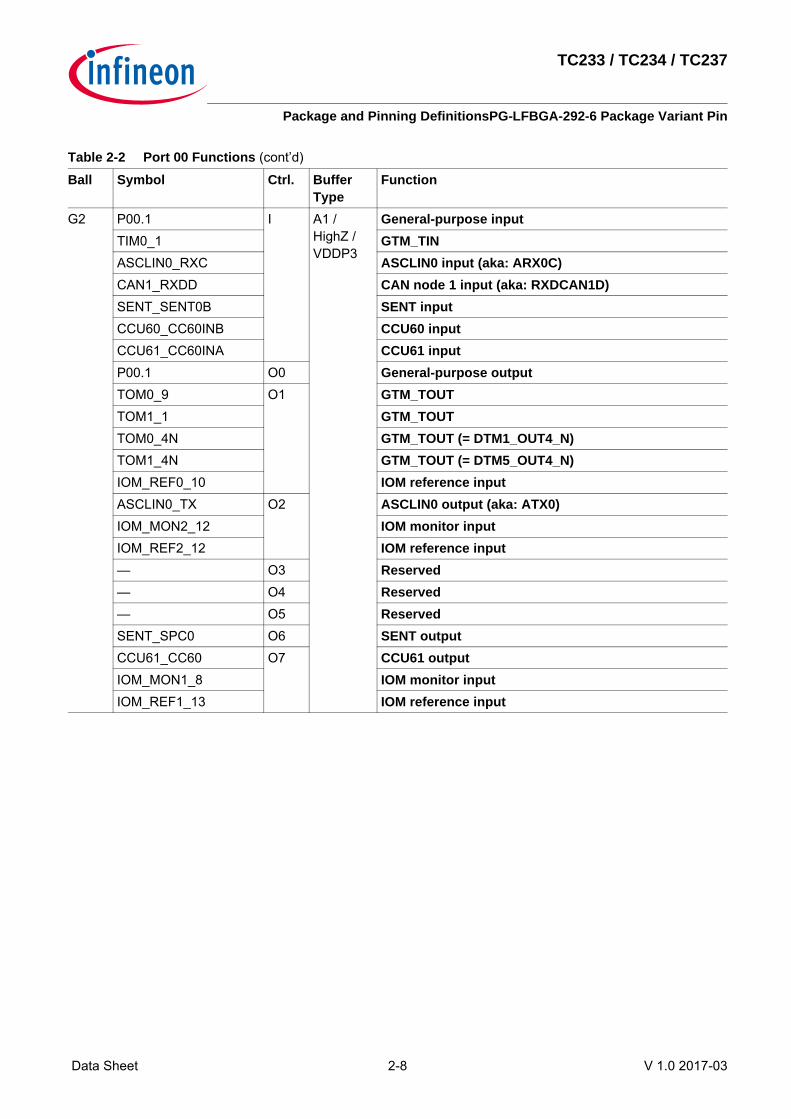
G2 P00.1 I A1 / HighZ / VDDP3
General-purpose inputTIM0_1 GTM_TINASCLIN0_RXC ASCLIN0 input (aka: ARX0C)CAN1_RXDD CAN node 1 input (aka: RXDCAN1D)SENT_SENT0B SENT inputCCU60_CC60INB CCU60 inputCCU61_CC60INA CCU61 inputP00.1 O0 General-purpose outputTOM0_9 O1 GTM_TOUTTOM1_1 GTM_TOUTTOM0_4N GTM_TOUT (= DTM1_OUT4_N)TOM1_4N GTM_TOUT (= DTM5_OUT4_N)IOM_REF0_10 IOM reference inputASCLIN0_TX O2 ASCLIN0 output (aka: ATX0)IOM_MON2_12 IOM monitor inputIOM_REF2_12 IOM reference input— O3 Reserved— O4 Reserved— O5 ReservedSENT_SPC0 O6 SENT outputCCU61_CC60 O7 CCU61 outputIOM_MON1_8 IOM monitor inputIOM_REF1_13 IOM reference input
Table 2-2 Port 00 Functions (cont’d)
Ball Symbol Ctrl. Buffer Type
Function

TC233 / TC234 / TC237
Package and Pinning DefinitionsPG-LFBGA-292-6 Package Variant Pin
Data Sheet 2-9 V 1.0 2017-03
H1 P00.2 I A1 / HighZ / VDDP3
General-purpose inputTIM0_1 GTM_TINSENT_SENT1B SENT inputP00.2 O0 General-purpose outputTOM0_9 O1 GTM_TOUTTOM1_1 GTM_TOUTTOM0_5 GTM_TOUT (= DTM1_OUT5)TOM1_5 GTM_TOUT (= DTM5_OUT5)IOM_REF0_11 IOM reference inputASCLIN0_SCLK O2 ASCLIN0 output (aka: ASCLK0)— O3 Reserved— O4 ReservedCAN12_TXD O5 CAN1 node 2 output (aka: TXDCAN12)— O6 ReservedCCU61_COUT60 O7 CCU61 outputIOM_MON1_11 IOM monitor inputIOM_REF1_10 IOM reference input
H2 P00.3 I A1 / HighZ / VDDP3
General-purpose inputSENT_SENT2B SENT inputCCU60_CC61INB CCU60 inputCCU61_CC61INA CCU61 inputCAN11_RXDA CAN1 node 1 input (aka: RXDCAN11A)CAN12_RXDA CAN1 node 2 input (aka: RXDCAN12A)P00.3 O0 General-purpose outputTOM0_10 O1 GTM_TOUTTOM1_2 GTM_TOUTTOM0_5N GTM_TOUT (= DTM1_OUT5_N)TOM1_5N GTM_TOUT (= DTM5_OUT5_N)IOM_REF0_12 IOM reference input— O2 Reserved— O3 Reserved— O4 Reserved— O5 ReservedSENT_SPC2 O6 SENT outputCCU61_CC61 O7 CCU61 outputIOM_MON1_9 IOM monitor inputIOM_REF1_12 IOM reference input
Table 2-2 Port 00 Functions (cont’d)
Ball Symbol Ctrl. Buffer Type
Function

TC233 / TC234 / TC237
Package and Pinning DefinitionsPG-LFBGA-292-6 Package Variant Pin
Data Sheet 2-10 V 1.0 2017-03
J1 P00.4 I A1 / HighZ / VDDP3
General-purpose inputSCU_REQ7 SCU inputSENT_SENT3B SENT inputP00.4 O0 General-purpose outputTOM0_11 O1 GTM_TOUTTOM1_3 GTM_TOUTTOM0_6 GTM_TOUT (= DTM1_OUT6)TOM1_6 GTM_TOUT (= DTM5_OUT6)IOM_REF0_13 IOM reference input— O2 ReservedCAN10_TXD O3 CAN1 node 0 output (aka: TXDCAN10)— O4 ReservedVADC_G1BFL0 O5 VADC outputSENT_SPC3 O6 SENT outputCCU61_COUT61 O7 CCU61 outputIOM_MON1_12 IOM monitor inputIOM_REF1_9 IOM reference input
J2 P00.5 I A1 / HighZ / VDDP3
General-purpose inputCCU60_CC62INB CCU60 inputCCU61_CC62INA CCU61 inputCAN10_RXDG CAN1 node 0 input (aka: RXDCAN10G)P00.5 O0 General-purpose outputTOM0_12 O1 GTM_TOUTTOM1_4 GTM_TOUT (= DTM5_OUT4)TOM0_6N GTM_TOUT (= DTM1_OUT6_N)TOM1_6N GTM_TOUT (= DTM5_OUT6_N)IOM_REF0_14 IOM reference input— O2 Reserved— O3 Reserved— O4 ReservedVADC_G1BFL1 O5 VADC output— O6 ReservedCCU61_CC62 O7 CCU61 outputIOM_MON1_10 IOM monitor inputIOM_REF1_11 IOM reference input
Table 2-2 Port 00 Functions (cont’d)
Ball Symbol Ctrl. Buffer Type
Function

TC233 / TC234 / TC237
Package and Pinning DefinitionsPG-LFBGA-292-6 Package Variant Pin
Data Sheet 2-11 V 1.0 2017-03
J4 P00.6 I A1 / HighZ / VDDP3
General-purpose inputCAN11_RXDG CAN1 node 1 input (aka: RXDCAN11G)P00.6 O0 General-purpose outputTOM0_13 O1 GTM_TOUTTOM1_5 GTM_TOUT (= DTM5_OUT5)TOM0_7 GTM_TOUT (= DTM1_OUT7)TOM1_7 GTM_TOUT (= DTM5_OUT7)IOM_REF0_15 IOM reference input— O2 ReservedVADC_G1BFL2 O3 VADC output— O4 ReservedVADC_EMUX10 O5 VADC output— O6 ReservedCCU61_COUT62 O7 CCU61 outputIOM_MON1_13 IOM monitor inputIOM_REF1_8 IOM reference input
K1 P00.7 I A1 / HighZ / VDDP3
General-purpose inputCCU61_CC60INC CCU61 inputCCU61_CCPOS0A CCU61 inputCCU60_T12HRB CCU60 inputGPT120_T2INA GPT120 inputP00.7 O0 General-purpose outputTOM0_14 O1 GTM_TOUTTOM1_6 GTM_TOUT (= DTM5_OUT6)TOM0_7N GTM_TOUT (= DTM1_OUT7_N)TOM1_7N GTM_TOUT (= DTM5_OUT7_N)CAN11_TXD O2 CAN1 node 1 output (aka: TXDCAN11)VADC_G1BFL3 O3 VADC output— O4 ReservedVADC_EMUX11 O5 VADC output— O6 ReservedCCU61_CC60 O7 CCU61 outputIOM_MON1_8 IOM monitor inputIOM_REF1_13 IOM reference input
Table 2-2 Port 00 Functions (cont’d)
Ball Symbol Ctrl. Buffer Type
Function

TC233 / TC234 / TC237
Package and Pinning DefinitionsPG-LFBGA-292-6 Package Variant Pin
Data Sheet 2-12 V 1.0 2017-03
K4 P00.8 I A1 / HighZ / VDDP3
General-purpose inputCCU61_CC61INC CCU61 inputCCU61_CCPOS1A CCU61 inputCCU60_T13HRB CCU60 inputGPT120_T2EUDA GPT120 inputCAN12_RXDG CAN1 node 2 input (aka: RXDCAN12G)P00.8 O0 General-purpose outputTOM0_15 O1 GTM_TOUTTOM1_7 GTM_TOUT (= DTM5_OUT7)QSPI3_SLSO6 O2 QSPI3 output (aka: SLSO36)— O3 Reserved— O4 ReservedVADC_EMUX12 O5 VADC output— O6 ReservedCCU61_CC61 O7 CCU61 outputIOM_MON1_9 IOM monitor inputIOM_REF1_12 IOM reference input
K2 P00.9 I A1 / HighZ / VDDP3
General-purpose inputTIM0_0 GTM_TINCCU61_CC62INC CCU61 inputCCU61_CCPOS2A CCU61 inputCCU60_T13HRC CCU60 inputCCU60_T12HRC CCU60 inputGPT120_T4EUDA GPT120 inputP00.9 O0 General-purpose outputTOM0_0 O1 GTM_TOUTTOM1_0 GTM_TOUTQSPI3_SLSO7 O2 QSPI3 output (aka: SLSO37)ASCLIN0_RTS O3 ASCLIN0 output (aka: ARTS0)— O4 ReservedCAN12_TXD O5 CAN1 node 2 output (aka: TXDCAN12)— O6 ReservedCCU61_CC62 O7 CCU61 outputIOM_MON1_10 IOM monitor inputIOM_REF1_11 IOM reference input
Table 2-2 Port 00 Functions (cont’d)
Ball Symbol Ctrl. Buffer Type
Function

TC233 / TC234 / TC237
Package and Pinning DefinitionsPG-LFBGA-292-6 Package Variant Pin
Data Sheet 2-13 V 1.0 2017-03
L2 P00.12 I A1 / HighZ / VDDP3
General-purpose inputTIM0_3 GTM_TINASCLIN0_CTSA ASCLIN0 input (aka: ACTS0A)P00.12 O0 General-purpose outputTOM0_3 O1 GTM_TOUTTOM1_3 GTM_TOUT— O2 Reserved— O3 Reserved— O4 Reserved— O5 Reserved— O6 ReservedCCU61_COUT63 O7 CCU61 outputIOM_MON1_7 IOM monitor inputIOM_REF1_7 IOM reference input
Table 2-2 Port 00 Functions (cont’d)
Ball Symbol Ctrl. Buffer Type
Function

TC233 / TC234 / TC237
Package and Pinning DefinitionsPG-LFBGA-292-6 Package Variant Pin
Data Sheet 2-14 V 1.0 2017-03
Table 2-3 Port 02 FunctionsBall Symbol Ctrl. Buffer
TypeFunction
B1 P02.0 I A1+ / HighZ / VDDP3
General-purpose inputTIM0_0 GTM_TINSCU_REQ6 SCU inputCCU60_CC60INA CCU60 inputCCU61_CC60INB CCU61 inputP02.0 O0 General-purpose outputTOM0_8 O1 GTM_TOUTTOM1_8 GTM_TOUTTOM0_4 GTM_TOUT (= DTM1_OUT4)TOM1_4 GTM_TOUT (= DTM5_OUT4)IOM_REF0_0 IOM reference input— O2 ReservedQSPI3_SLSO1 O3 QSPI3 output (aka: SLSO31)— O4 ReservedCAN0_TXD O5 CAN node 0 output (aka: TXDCAN0)IOM_MON2_5 IOM monitor inputIOM_REF2_5 IOM reference inputERAY0_TXDA O6 ERAY0 outputCCU60_CC60 O7 CCU60 outputIOM_MON1_2 IOM monitor inputIOM_REF1_6 IOM reference input
TC233 / TC234 / TC237
Package and Pinning DefinitionsPG-LFBGA-292-6 Package Variant Pin
Data Sheet 2-15 V 1.0 2017-03
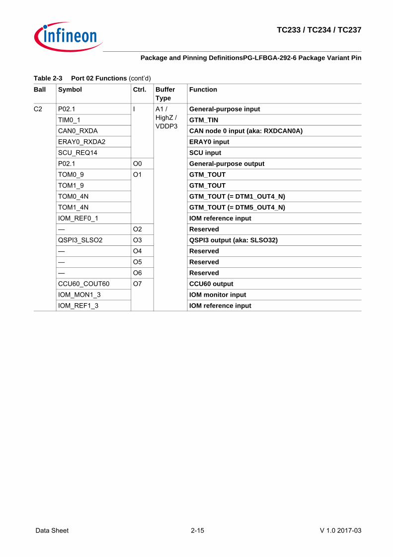
C2 P02.1 I A1 / HighZ / VDDP3
General-purpose inputTIM0_1 GTM_TINCAN0_RXDA CAN node 0 input (aka: RXDCAN0A)ERAY0_RXDA2 ERAY0 inputSCU_REQ14 SCU inputP02.1 O0 General-purpose outputTOM0_9 O1 GTM_TOUTTOM1_9 GTM_TOUTTOM0_4N GTM_TOUT (= DTM1_OUT4_N)TOM1_4N GTM_TOUT (= DTM5_OUT4_N)IOM_REF0_1 IOM reference input— O2 ReservedQSPI3_SLSO2 O3 QSPI3 output (aka: SLSO32)— O4 Reserved— O5 Reserved— O6 ReservedCCU60_COUT60 O7 CCU60 outputIOM_MON1_3 IOM monitor inputIOM_REF1_3 IOM reference input
Table 2-3 Port 02 Functions (cont’d)
Ball Symbol Ctrl. Buffer Type
Function

TC233 / TC234 / TC237
Package and Pinning DefinitionsPG-LFBGA-292-6 Package Variant Pin
Data Sheet 2-16 V 1.0 2017-03
C1 P02.2 I A1+ / HighZ / VDDP3
General-purpose inputTIM0_2 GTM_TINCCU60_CC61INA CCU60 inputCCU61_CC61INB CCU61 inputP02.2 O0 General-purpose outputTOM0_10 O1 GTM_TOUTTOM1_10 GTM_TOUTTOM0_5 GTM_TOUT (= DTM1_OUT5)TOM1_5 GTM_TOUT (= DTM5_OUT5)IOM_REF0_2 IOM reference inputASCLIN1_TX O2 ASCLIN1 output (aka: ATX1)IOM_MON2_13 IOM monitor inputIOM_REF2_13 IOM reference inputQSPI3_SLSO3 O3 QSPI3 output (aka: SLSO33)— O4 ReservedCAN2_TXD O5 CAN node 2 output (aka: TXDCAN2)IOM_MON2_7 IOM monitor inputIOM_REF2_7 IOM reference inputERAY0_TXDB O6 ERAY0 outputCCU60_CC61 O7 CCU60 outputIOM_MON1_1 IOM monitor inputIOM_REF1_5 IOM reference input
Table 2-3 Port 02 Functions (cont’d)
Ball Symbol Ctrl. Buffer Type
Function
TC233 / TC234 / TC237
Package and Pinning DefinitionsPG-LFBGA-292-6 Package Variant Pin
Data Sheet 2-17 V 1.0 2017-03
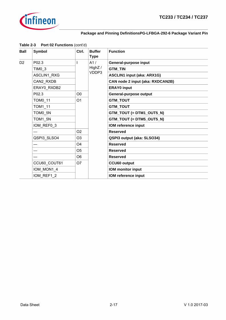
D2 P02.3 I A1 / HighZ / VDDP3
General-purpose inputTIM0_3 GTM_TINASCLIN1_RXG ASCLIN1 input (aka: ARX1G)CAN2_RXDB CAN node 2 input (aka: RXDCAN2B)ERAY0_RXDB2 ERAY0 inputP02.3 O0 General-purpose outputTOM0_11 O1 GTM_TOUTTOM1_11 GTM_TOUTTOM0_5N GTM_TOUT (= DTM1_OUT5_N)TOM1_5N GTM_TOUT (= DTM5_OUT5_N)IOM_REF0_3 IOM reference input— O2 ReservedQSPI3_SLSO4 O3 QSPI3 output (aka: SLSO34)— O4 Reserved— O5 Reserved— O6 ReservedCCU60_COUT61 O7 CCU60 outputIOM_MON1_4 IOM monitor inputIOM_REF1_2 IOM reference input
Table 2-3 Port 02 Functions (cont’d)
Ball Symbol Ctrl. Buffer Type
Function

TC233 / TC234 / TC237
Package and Pinning DefinitionsPG-LFBGA-292-6 Package Variant Pin
Data Sheet 2-18 V 1.0 2017-03
D1 P02.4 I A1+ / HighZ / VDDP3
General-purpose inputTIM0_4 GTM_TINQSPI3_SLSIA QSPI3 input (aka: SLSI3A)CAN0_RXDD CAN node 0 input (aka: RXDCAN0D)CCU60_CC62INA CCU60 inputCCU61_CC62INB CCU61 inputP02.4 O0 General-purpose outputTOM0_12 O1 GTM_TOUTTOM1_12 GTM_TOUTTOM0_6 GTM_TOUT (= DTM1_OUT6)TOM1_6 GTM_TOUT (= DTM5_OUT6)IOM_REF0_4 IOM reference input— O2 ReservedQSPI3_SLSO0 O3 QSPI3 output (aka: SLSO30)— O4 ReservedCAN10_TXD O5 CAN1 node 0 output (aka: TXDCAN10)ERAY0_TXENA O6 ERAY0 outputCCU60_CC62 O7 CCU60 outputIOM_MON1_0 IOM monitor inputIOM_REF1_4 IOM reference input
Table 2-3 Port 02 Functions (cont’d)
Ball Symbol Ctrl. Buffer Type
Function

TC233 / TC234 / TC237
Package and Pinning DefinitionsPG-LFBGA-292-6 Package Variant Pin
Data Sheet 2-19 V 1.0 2017-03
E2 P02.5 I A1+ / HighZ / VDDP3
General-purpose inputTIM0_5 GTM_TINQSPI3_MRSTA QSPI3 input (aka: MRST3A)SENT_SENT3C SENT inputP02.5 O0 General-purpose outputTOM0_13 O1 GTM_TOUTTOM1_13 GTM_TOUTTOM0_6N GTM_TOUT (= DTM1_OUT6_N)TOM1_6N GTM_TOUT (= DTM5_OUT6_N)IOM_REF0_5 IOM reference inputCAN0_TXD O2 CAN node 0 output (aka: TXDCAN0)IOM_MON2_5 IOM monitor inputIOM_REF2_5 IOM reference inputQSPI3_MRST O3 QSPI3 output (aka: MRST3)IOM_MON2_3 IOM monitor inputIOM_REF2_3 IOM reference input— O4 ReservedCAN11_TXD O5 CAN1 node 1 output (aka: TXDCAN11)ERAY0_TXENB O6 ERAY0 outputCCU60_COUT62 O7 CCU60 outputIOM_MON1_5 IOM monitor inputIOM_REF1_1 IOM reference input
Table 2-3 Port 02 Functions (cont’d)
Ball Symbol Ctrl. Buffer Type
Function

TC233 / TC234 / TC237
Package and Pinning DefinitionsPG-LFBGA-292-6 Package Variant Pin
Data Sheet 2-20 V 1.0 2017-03
E1 P02.6 I A1 / HighZ / VDDP3
General-purpose inputTIM0_6 GTM_TINQSPI3_MTSRA QSPI3 input (aka: MTSR3A)SENT_SENT2C SENT inputCCU60_CC60INC CCU60 inputCCU60_CCPOS0A CCU60 inputCCU61_T12HRB CCU61 inputGPT120_T3INA GPT120 inputCAN10_RXDF CAN1 node 0 input (aka: RXDCAN10F)P02.6 O0 General-purpose outputTOM0_14 O1 GTM_TOUTTOM1_14 GTM_TOUTTOM0_7 GTM_TOUT (= DTM1_OUT7)TOM1_7 GTM_TOUT (= DTM5_OUT7)IOM_REF0_6 IOM reference input— O2 ReservedQSPI3_MTSR O3 QSPI3 output (aka: MTSR3)— O4 ReservedVADC_EMUX00 O5 VADC output— O6 ReservedCCU60_CC60 O7 CCU60 outputIOM_MON1_2 IOM monitor inputIOM_REF1_6 IOM reference input
Table 2-3 Port 02 Functions (cont’d)
Ball Symbol Ctrl. Buffer Type
Function

TC233 / TC234 / TC237
Package and Pinning DefinitionsPG-LFBGA-292-6 Package Variant Pin
Data Sheet 2-21 V 1.0 2017-03
F2 P02.7 I A1 / HighZ / VDDP3
General-purpose inputTIM0_7 GTM_TINQSPI3_SCLKA QSPI3 input (aka: SCLK3A)SENT_SENT1C SENT inputCCU60_CC61INC CCU60 inputCCU60_CCPOS1A CCU60 inputCCU61_T13HRB CCU61 inputGPT120_T3EUDA GPT120 inputCAN11_RXDF CAN1 node 1 input (aka: RXDCAN11F)PMU_FDEST PMU inputP02.7 O0 General-purpose outputTOM0_15 O1 GTM_TOUTTOM1_15 GTM_TOUTTOM0_7N GTM_TOUT (= DTM1_OUT7_N)TOM1_7N GTM_TOUT (= DTM5_OUT7_N)IOM_REF0_7 IOM reference input— O2 ReservedQSPI3_SCLK O3 QSPI3 output (aka: SCLK3)— O4 ReservedVADC_EMUX01 O5 VADC outputSENT_SPC1 O6 SENT outputCCU60_CC61 O7 CCU60 outputIOM_MON1_1 IOM monitor inputIOM_REF1_5 IOM reference input
Table 2-3 Port 02 Functions (cont’d)
Ball Symbol Ctrl. Buffer Type
Function

TC233 / TC234 / TC237
Package and Pinning DefinitionsPG-LFBGA-292-6 Package Variant Pin
Data Sheet 2-22 V 1.0 2017-03
F1 P02.8 I A1 / HighZ / VDDP3
General-purpose inputTIM0_0 GTM_TINSENT_SENT0C SENT inputCCU60_CC62INC CCU60 inputCCU60_CCPOS2A CCU60 inputCCU61_T12HRC CCU61 inputCCU61_T13HRC CCU61 inputGPT120_T4INA GPT120 inputP02.8 O0 General-purpose outputTOM0_8 O1 GTM_TOUTTOM1_0 GTM_TOUTTOM0_4N GTM_TOUT (= DTM1_OUT4_N)TOM1_4N GTM_TOUT (= DTM5_OUT4_N)IOM_REF0_8 IOM reference inputQSPI3_SLSO5 O2 QSPI3 output (aka: SLSO35)— O3 Reserved— O4 ReservedVADC_EMUX02 O5 VADC output— O6 ReservedCCU60_CC62 O7 CCU60 outputIOM_MON1_0 IOM monitor inputIOM_REF1_4 IOM reference input
Table 2-3 Port 02 Functions (cont’d)
Ball Symbol Ctrl. Buffer Type
Function

TC233 / TC234 / TC237
Package and Pinning DefinitionsPG-LFBGA-292-6 Package Variant Pin
Data Sheet 2-23 V 1.0 2017-03
Table 2-4 Port 10 FunctionsBall Symbol Ctrl. Buffer
TypeFunction
B7 P10.1 I A1 / HighZ / VDDP3
General-purpose inputTIM0_1 GTM_TINQSPI1_MRSTA QSPI1 input (aka: MRST1A)GPT120_T5EUDB GPT120 inputP10.1 O0 General-purpose outputTOM0_1 O1 GTM_TOUTTOM1_9 GTM_TOUTQSPI1_MTSR O2 QSPI1 output (aka: MTSR1)QSPI1_MRST O3 QSPI1 output (aka: MRST1)IOM_MON2_1 IOM monitor inputIOM_REF2_1 IOM reference input— O4 Reserved— O5 Reserved— O6 Reserved— O7 Reserved
A5 P10.2 I A1 / HighZ / VDDP3
General-purpose inputTIM0_2 GTM_TINQSPI1_SCLKA QSPI1 input (aka: SCLK1A)CAN2_RXDE CAN node 2 input (aka: RXDCAN2E)SCU_REQ2 SCU inputGPT120_T6INB GPT120 inputP10.2 O0 General-purpose outputTOM0_2 O1 GTM_TOUTTOM1_10 GTM_TOUTIOM_MON2_9 IOM monitor input— O2 ReservedQSPI1_SCLK O3 QSPI1 output (aka: SCLK1)— O4 Reserved— O5 Reserved— O6 Reserved— O7 Reserved

TC233 / TC234 / TC237
Package and Pinning DefinitionsPG-LFBGA-292-6 Package Variant Pin
Data Sheet 2-24 V 1.0 2017-03
A6 P10.3 I A1 / HighZ / VDDP3
General-purpose inputTIM0_3 GTM_TINQSPI1_MTSRA QSPI1 input (aka: MTSR1A)SCU_REQ3 SCU inputGPT120_T5INB GPT120 inputP10.3 O0 General-purpose outputTOM0_3 O1 GTM_TOUTTOM1_11 GTM_TOUTIOM_MON2_10 IOM monitor input— O2 ReservedQSPI1_MTSR O3 QSPI1 output (aka: MTSR1)— O4 Reserved— O5 ReservedCAN2_TXD O6 CAN node 2 output (aka: TXDCAN2)IOM_MON2_7 IOM monitor inputIOM_REF2_7 IOM reference input— O7 Reserved
B5 P10.5 I A1 / HighZ / VDDP3
General-purpose inputTIM0_2 GTM_TINSCU_HWCFG4 SCU inputCAN10_RXDA CAN1 node 0 input (aka: RXDCAN10A)P10.5 O0 General-purpose outputTOM0_2 O1 GTM_TOUTTOM1_10 GTM_TOUTIOM_REF2_9 IOM reference input— O2 ReservedQSPI3_SLSO8 O3 QSPI3 output (aka: SLSO38)QSPI1_SLSO9 O4 QSPI1 output (aka: SLSO19)GPT120_T6OUT O5 GPT120 output— O6 Reserved— O7 Reserved
Table 2-4 Port 10 Functions (cont’d)
Ball Symbol Ctrl. Buffer Type
Function

TC233 / TC234 / TC237
Package and Pinning DefinitionsPG-LFBGA-292-6 Package Variant Pin
Data Sheet 2-25 V 1.0 2017-03
A4 P10.6 I A1 / HighZ / VDDP3
General-purpose inputTIM0_3 GTM_TINQSPI3_MTSRB QSPI3 input (aka: MTSR3B)SCU_HWCFG5 SCU inputP10.6 O0 General-purpose outputTOM0_3 O1 GTM_TOUTTOM1_11 GTM_TOUTIOM_REF2_10 IOM reference input— O2 ReservedQSPI3_MTSR O3 QSPI3 output (aka: MTSR3)GPT120_T3OUT O4 GPT120 outputCAN10_TXD O5 CAN1 node 0 output (aka: TXDCAN10)QSPI1_MRST O6 QSPI1 output (aka: MRST1)IOM_MON2_1 IOM monitor inputIOM_REF2_1 IOM reference input— O7 Reserved
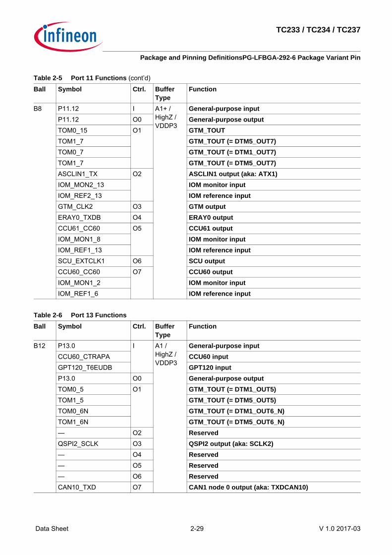
Table 2-5 Port 11 FunctionsBall Symbol Ctrl. Buffer
TypeFunction
A10 P11.2 I A1+ / HighZ / VDDP3
General-purpose inputP11.2 O0 General-purpose outputTOM0_8 O1 GTM_TOUTTOM1_1 GTM_TOUTTOM0_4N GTM_TOUT (= DTM1_OUT4_N)TOM1_4N GTM_TOUT (= DTM5_OUT4_N)— O2 ReservedQSPI0_SLSO5 O3 QSPI0 output (aka: SLSO05)QSPI1_SLSO5 O4 QSPI1 output (aka: SLSO15)CCU61_COUT63 O5 CCU61 outputIOM_MON1_7 IOM monitor inputIOM_REF1_7 IOM reference input— O6 ReservedCCU60_COUT63 O7 CCU60 outputIOM_MON1_6 IOM monitor inputIOM_REF1_0 IOM reference input
Table 2-4 Port 10 Functions (cont’d)
Ball Symbol Ctrl. Buffer Type
Function

TC233 / TC234 / TC237
Package and Pinning DefinitionsPG-LFBGA-292-6 Package Variant Pin
Data Sheet 2-26 V 1.0 2017-03
B10 P11.3 I A1+ / HighZ / VDDP3
General-purpose inputQSPI1_MRSTB QSPI1 input (aka: MRST1B)P11.3 O0 General-purpose outputTOM0_10 O1 GTM_TOUTTOM1_2 GTM_TOUTTOM0_5 GTM_TOUT (= DTM1_OUT5)TOM1_5 GTM_TOUT (= DTM5_OUT5)— O2 ReservedQSPI1_MRST O3 QSPI1 output (aka: MRST1)IOM_MON2_1 IOM monitor inputIOM_REF2_1 IOM reference inputERAY0_TXDA O4 ERAY0 outputCCU61_COUT62 O5 CCU61 outputIOM_MON1_13 IOM monitor inputIOM_REF1_8 IOM reference input— O6 ReservedCCU60_COUT62 O7 CCU60 outputIOM_MON1_5 IOM monitor inputIOM_REF1_1 IOM reference input
D9 P11.6 I A1+ / HighZ / VDDP3
General-purpose inputQSPI1_SCLKB QSPI1 input (aka: SCLK1B)P11.6 O0 General-purpose outputTOM0_11 O1 GTM_TOUTTOM1_3 GTM_TOUTTOM0_5N GTM_TOUT (= DTM1_OUT5_N)TOM1_5N GTM_TOUT (= DTM5_OUT5_N)ERAY0_TXENB O2 ERAY0 outputQSPI1_SCLK O3 QSPI1 output (aka: SCLK1)ERAY0_TXENA O4 ERAY0 outputCCU61_COUT61 O5 CCU61 outputIOM_MON1_12 IOM monitor inputIOM_REF1_9 IOM reference input— O6 ReservedCCU60_COUT61 O7 CCU60 outputIOM_MON1_4 IOM monitor inputIOM_REF1_2 IOM reference input
Table 2-5 Port 11 Functions (cont’d)
Ball Symbol Ctrl. Buffer Type
Function

TC233 / TC234 / TC237
Package and Pinning DefinitionsPG-LFBGA-292-6 Package Variant Pin
Data Sheet 2-27 V 1.0 2017-03
E7 P11.8 I A1 / HighZ / VDDP3
General-purpose inputQSPI1_MTSRC QSPI1 input (aka: MTSR1C)P11.8 O0 General-purpose outputTOM0_4 O1 GTM_TOUT (= DTM1_OUT4)TOM1_4 GTM_TOUT (= DTM5_OUT4)— O2 ReservedQSPI1_SLSO10 O3 QSPI1 output (aka: SLSO110)QSPI1_MTSR O4 QSPI1 output (aka: MTSR1)— O5 Reserved— O6 Reserved— O7 Reserved
A9 P11.9 I A1+ / HighZ / VDDP3
General-purpose inputQSPI1_MTSRB QSPI1 input (aka: MTSR1B)ERAY0_RXDA1 ERAY0 inputP11.9 O0 General-purpose outputTOM0_12 O1 GTM_TOUTTOM1_4 GTM_TOUT (= DTM5_OUT4)TOM0_6 GTM_TOUT (= DTM1_OUT6)TOM1_6 GTM_TOUT (= DTM5_OUT6)— O2 ReservedQSPI1_MTSR O3 QSPI1 output (aka: MTSR1)— O4 ReservedCCU61_COUT60 O5 CCU61 outputIOM_MON1_11 IOM monitor inputIOM_REF1_10 IOM reference input— O6 ReservedCCU60_COUT60 O7 CCU60 outputIOM_MON1_3 IOM monitor inputIOM_REF1_3 IOM reference input
Table 2-5 Port 11 Functions (cont’d)
Ball Symbol Ctrl. Buffer Type
Function

TC233 / TC234 / TC237
Package and Pinning DefinitionsPG-LFBGA-292-6 Package Variant Pin
Data Sheet 2-28 V 1.0 2017-03
B9 P11.10 I A1+ / HighZ / VDDP3
General-purpose inputASCLIN1_RXE ASCLIN1 input (aka: ARX1E)ERAY0_RXDB1 ERAY0 inputSCU_REQ12 SCU inputCAN12_RXDD CAN1 node 2 input (aka: RXDCAN12D)P11.10 O0 General-purpose outputTOM0_13 O1 GTM_TOUTTOM1_5 GTM_TOUT (= DTM5_OUT5)TOM0_6N GTM_TOUT (= DTM1_OUT6_N)TOM1_6N GTM_TOUT (= DTM5_OUT6_N)— O2 ReservedQSPI0_SLSO3 O3 QSPI0 output (aka: SLSO03)QSPI1_SLSO3 O4 QSPI1 output (aka: SLSO13)CCU61_CC62 O5 CCU61 outputIOM_MON1_10 IOM monitor inputIOM_REF1_11 IOM reference input— O6 ReservedCCU60_CC62 O7 CCU60 outputIOM_MON1_0 IOM monitor inputIOM_REF1_4 IOM reference input
A8 P11.11 I A1+ / HighZ / VDDP3
General-purpose inputP11.11 O0 General-purpose outputTOM0_14 O1 GTM_TOUTTOM1_6 GTM_TOUT (= DTM5_OUT6)TOM0_7N GTM_TOUT (= DTM1_OUT7_N)TOM1_7N GTM_TOUT (= DTM5_OUT7_N)— O2 ReservedQSPI0_SLSO4 O3 QSPI0 output (aka: SLSO04)QSPI1_SLSO4 O4 QSPI1 output (aka: SLSO14)CCU61_CC61 O5 CCU61 outputIOM_MON1_9 IOM monitor inputIOM_REF1_12 IOM reference inputERAY0_TXENB O6 ERAY0 outputCCU60_CC61 O7 CCU60 outputIOM_MON1_1 IOM monitor inputIOM_REF1_5 IOM reference input
Table 2-5 Port 11 Functions (cont’d)
Ball Symbol Ctrl. Buffer Type
Function
TC233 / TC234 / TC237
Package and Pinning DefinitionsPG-LFBGA-292-6 Package Variant Pin
Data Sheet 2-29 V 1.0 2017-03
B8 P11.12 I A1+ / HighZ / VDDP3
General-purpose inputP11.12 O0 General-purpose outputTOM0_15 O1 GTM_TOUTTOM1_7 GTM_TOUT (= DTM5_OUT7)TOM0_7 GTM_TOUT (= DTM1_OUT7)TOM1_7 GTM_TOUT (= DTM5_OUT7)ASCLIN1_TX O2 ASCLIN1 output (aka: ATX1)IOM_MON2_13 IOM monitor inputIOM_REF2_13 IOM reference inputGTM_CLK2 O3 GTM outputERAY0_TXDB O4 ERAY0 outputCCU61_CC60 O5 CCU61 outputIOM_MON1_8 IOM monitor inputIOM_REF1_13 IOM reference inputSCU_EXTCLK1 O6 SCU outputCCU60_CC60 O7 CCU60 outputIOM_MON1_2 IOM monitor inputIOM_REF1_6 IOM reference input
Table 2-6 Port 13 FunctionsBall Symbol Ctrl. Buffer
TypeFunction
B12 P13.0 I A1 / HighZ / VDDP3
General-purpose inputCCU60_CTRAPA CCU60 inputGPT120_T6EUDB GPT120 inputP13.0 O0 General-purpose outputTOM0_5 O1 GTM_TOUT (= DTM1_OUT5)TOM1_5 GTM_TOUT (= DTM5_OUT5)TOM0_6N GTM_TOUT (= DTM1_OUT6_N)TOM1_6N GTM_TOUT (= DTM5_OUT6_N)— O2 ReservedQSPI2_SCLK O3 QSPI2 output (aka: SCLK2)— O4 Reserved— O5 Reserved— O6 ReservedCAN10_TXD O7 CAN1 node 0 output (aka: TXDCAN10)
Table 2-5 Port 11 Functions (cont’d)
Ball Symbol Ctrl. Buffer Type
Function

TC233 / TC234 / TC237
Package and Pinning DefinitionsPG-LFBGA-292-6 Package Variant Pin
Data Sheet 2-30 V 1.0 2017-03
A12 P13.1 I A1 / HighZ / VDDP3
General-purpose inputCCU60_CCPOS0C CCU60 inputGPT120_T3INB GPT120 inputCAN10_RXDB CAN1 node 0 input (aka: RXDCAN10B)P13.1 O0 General-purpose outputTOM0_6 O1 GTM_TOUT (= DTM1_OUT6)TOM1_6 GTM_TOUT (= DTM5_OUT6)TOM0_7 GTM_TOUT (= DTM1_OUT7)TOM1_7 GTM_TOUT (= DTM5_OUT7)— O2 Reserved— O3 Reserved— O4 Reserved— O5 Reserved— O6 Reserved— O7 Reserved
B11 P13.2 I A1 / HighZ / VDDP3
General-purpose inputCCU60_CCPOS1C CCU60 inputGPT120_T3EUDB GPT120 inputGPT120_CAPINA GPT120 inputP13.2 O0 General-purpose outputTOM0_7 O1 GTM_TOUT (= DTM1_OUT7)TOM1_7 GTM_TOUT (= DTM5_OUT7)TOM0_7N GTM_TOUT (= DTM1_OUT7_N)TOM1_7N GTM_TOUT (= DTM5_OUT7_N)CAN11_TXD O2 CAN1 node 1 output (aka: TXDCAN11)— O3 Reserved— O4 Reserved— O5 Reserved— O6 Reserved— O7 Reserved
Table 2-6 Port 13 Functions (cont’d)
Ball Symbol Ctrl. Buffer Type
Function

TC233 / TC234 / TC237
Package and Pinning DefinitionsPG-LFBGA-292-6 Package Variant Pin
Data Sheet 2-31 V 1.0 2017-03
A11 P13.3 I A1 / HighZ / VDDP3
General-purpose inputCCU60_CCPOS2C CCU60 inputGPT120_T4INB GPT120 inputCAN11_RXDB CAN1 node 1 input (aka: RXDCAN11B)P13.3 O0 General-purpose outputTOM0_8 O1 GTM_TOUTTOM1_0 GTM_TOUTTOM0_4 GTM_TOUT (= DTM1_OUT4)TOM1_4 GTM_TOUT (= DTM5_OUT4)— O2 ReservedQSPI2_MTSR O3 QSPI2 output (aka: MTSR2)— O4 Reserved— O5 Reserved— O6 Reserved— O7 Reserved
Table 2-7 Port 14 FunctionsBall Symbol Ctrl. Buffer
TypeFunction
B16 P14.0 I A1+ / HighZ / VDDP3
General-purpose inputTIM0_3 GTM_TINP14.0 O0 General-purpose outputTOM0_3 O1 GTM_TOUTTOM1_3 GTM_TOUTTOM0_6 GTM_TOUT (= DTM1_OUT6)TOM1_6 GTM_TOUT (= DTM5_OUT6)ASCLIN0_TX O2 ASCLIN0 output (aka: ATX0)IOM_MON2_12 IOM monitor inputIOM_REF2_12 IOM reference inputERAY0_TXDA O3 ERAY0 outputERAY0_TXDB O4 ERAY0 outputCAN1_TXD O5 CAN node 1 output (aka: TXDCAN1)IOM_MON2_6 IOM monitor inputIOM_REF2_6 IOM reference inputASCLIN0_SCLK O6 ASCLIN0 output (aka: ASCLK0)CCU60_COUT62 O7 CCU60 outputIOM_MON1_5 IOM monitor inputIOM_REF1_1 IOM reference input
Table 2-6 Port 13 Functions (cont’d)
Ball Symbol Ctrl. Buffer Type
Function

TC233 / TC234 / TC237
Package and Pinning DefinitionsPG-LFBGA-292-6 Package Variant Pin
Data Sheet 2-32 V 1.0 2017-03
A15 P14.1 I A1+ / HighZ / VDDP3
General-purpose inputTIM0_4 GTM_TINASCLIN0_RXA ASCLIN0 input (aka: ARX0A)CAN1_RXDB CAN node 1 input (aka: RXDCAN1B)ERAY0_RXDA3 ERAY0 inputSCU_REQ15 SCU inputERAY0_RXDB3 ERAY0 inputSCU_EVRWUPA AI SCU inputP14.1 O0 General-purpose outputTOM0_4 O1 GTM_TOUT (= DTM1_OUT4)TOM1_4 GTM_TOUT (= DTM5_OUT4)TOM0_7 GTM_TOUT (= DTM1_OUT7)TOM1_7 GTM_TOUT (= DTM5_OUT7)IOM_REF1_14 IOM reference inputASCLIN0_TX O2 ASCLIN0 output (aka: ATX0)IOM_MON2_12 IOM monitor inputIOM_REF2_12 IOM reference input— O3 Reserved— O4 Reserved— O5 Reserved— O6 ReservedCCU60_COUT63 O7 CCU60 outputIOM_MON1_6 IOM monitor inputIOM_REF1_0 IOM reference input
Table 2-7 Port 14 Functions (cont’d)
Ball Symbol Ctrl. Buffer Type
Function

TC233 / TC234 / TC237
Package and Pinning DefinitionsPG-LFBGA-292-6 Package Variant Pin
Data Sheet 2-33 V 1.0 2017-03
E13 P14.2 I A1 / PU / VDDP3
General-purpose inputTIM0_5 GTM_TINSCU_HWCFG2_EVR13 SCU inputP14.2 O0 General-purpose outputTOM0_5 O1 GTM_TOUT (= DTM1_OUT5)TOM1_5 GTM_TOUT (= DTM5_OUT5)TOM0_6N GTM_TOUT (= DTM1_OUT6_N)TOM1_6N GTM_TOUT (= DTM5_OUT6_N)IOM_REF1_15 IOM reference input— O2 ReservedQSPI2_SLSO1 O3 QSPI2 output (aka: SLSO21)— O4 Reserved— O5 Reserved— O6 Reserved— O7 Reserved
B14 P14.3 I A1 / PU / VDDP3
General-purpose inputTIM0_6 GTM_TINSCU_REQ10 SCU inputSCU_HWCFG3_BMI SCU inputP14.3 O0 General-purpose outputTOM0_6 O1 GTM_TOUT (= DTM1_OUT6)TOM1_6 GTM_TOUT (= DTM5_OUT6)IOM_REF2_4 IOM reference input— O2 ReservedQSPI2_SLSO3 O3 QSPI2 output (aka: SLSO23)ASCLIN1_SLSO O4 ASCLIN1 output (aka: ASLSO1)— O5 Reserved— O6 Reserved— O7 Reserved
Table 2-7 Port 14 Functions (cont’d)
Ball Symbol Ctrl. Buffer Type
Function

TC233 / TC234 / TC237
Package and Pinning DefinitionsPG-LFBGA-292-6 Package Variant Pin
Data Sheet 2-34 V 1.0 2017-03
B15 P14.4 I A1+ / HighZ / VDDP3
General-purpose inputTIM0_7 GTM_TINP14.4 O0 General-purpose outputTOM0_7 O1 GTM_TOUT (= DTM1_OUT7)TOM1_7 GTM_TOUT (= DTM5_OUT7)TOM0_7N GTM_TOUT (= DTM1_OUT7_N)TOM1_7N GTM_TOUT (= DTM5_OUT7_N)IOM_REF2_8 IOM reference input— O2 Reserved— O3 Reserved— O4 Reserved— O5 Reserved— O6 Reserved— O7 Reserved
A14 P14.5 I A1+ / HighZ / VDDP3
General-purpose inputTIM0_0 GTM_TINP14.5 O0 General-purpose outputTOM0_0 O1 GTM_TOUTTOM1_0 GTM_TOUTIOM_REF2_11 IOM reference input— O2 Reserved— O3 Reserved— O4 Reserved— O5 ReservedERAY0_TXDB O6 ERAY0 output— O7 Reserved
Table 2-7 Port 14 Functions (cont’d)
Ball Symbol Ctrl. Buffer Type
Function
TC233 / TC234 / TC237
Package and Pinning DefinitionsPG-LFBGA-292-6 Package Variant Pin
Data Sheet 2-35 V 1.0 2017-03
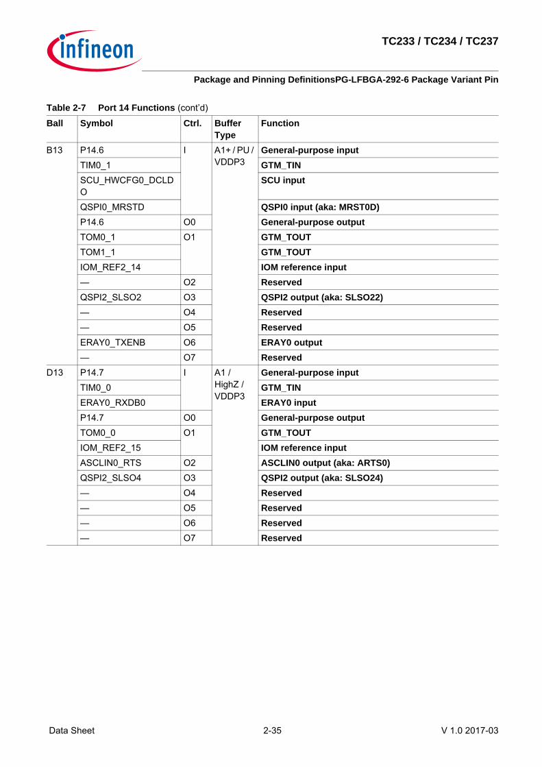
B13 P14.6 I A1+ / PU / VDDP3
General-purpose inputTIM0_1 GTM_TINSCU_HWCFG0_DCLDO
SCU input
QSPI0_MRSTD QSPI0 input (aka: MRST0D)P14.6 O0 General-purpose outputTOM0_1 O1 GTM_TOUTTOM1_1 GTM_TOUTIOM_REF2_14 IOM reference input— O2 ReservedQSPI2_SLSO2 O3 QSPI2 output (aka: SLSO22)— O4 Reserved— O5 ReservedERAY0_TXENB O6 ERAY0 output— O7 Reserved
D13 P14.7 I A1 / HighZ / VDDP3
General-purpose inputTIM0_0 GTM_TINERAY0_RXDB0 ERAY0 inputP14.7 O0 General-purpose outputTOM0_0 O1 GTM_TOUTIOM_REF2_15 IOM reference inputASCLIN0_RTS O2 ASCLIN0 output (aka: ARTS0)QSPI2_SLSO4 O3 QSPI2 output (aka: SLSO24)— O4 Reserved— O5 Reserved— O6 Reserved— O7 Reserved
Table 2-7 Port 14 Functions (cont’d)
Ball Symbol Ctrl. Buffer Type
Function

TC233 / TC234 / TC237
Package and Pinning DefinitionsPG-LFBGA-292-6 Package Variant Pin
Data Sheet 2-36 V 1.0 2017-03
A13 P14.8 I A1 / HighZ / VDDP3
General-purpose inputASCLIN1_RXD ASCLIN1 input (aka: ARX1D)CAN2_RXDD CAN node 2 input (aka: RXDCAN2D)ERAY0_RXDA0 ERAY0 inputP14.8 O0 General-purpose outputTOM0_2 O1 GTM_TOUT— O2 Reserved— O3 Reserved— O4 Reserved— O5 Reserved— O6 Reserved— O7 Reserved
Table 2-8 Port 15 FunctionsBall Symbol Ctrl. Buffer
TypeFunction
B20 P15.0 I A1 / HighZ / VDDP3
General-purpose inputP15.0 O0 General-purpose outputTOM1_3 O1 GTM_TOUTTOM0_11 GTM_TOUTTOM0_7N GTM_TOUT (= DTM1_OUT7_N)TOM1_7N GTM_TOUT (= DTM5_OUT7_N)ASCLIN1_TX O2 ASCLIN1 output (aka: ATX1)IOM_MON2_13 IOM monitor inputIOM_REF2_13 IOM reference inputQSPI0_SLSO13 O3 QSPI0 output (aka: SLSO013)— O4 ReservedCAN2_TXD O5 CAN node 2 output (aka: TXDCAN2)IOM_MON2_7 IOM monitor inputIOM_REF2_7 IOM reference inputASCLIN1_SCLK O6 ASCLIN1 output (aka: ASCLK1)— O7 Reserved
Table 2-7 Port 14 Functions (cont’d)
Ball Symbol Ctrl. Buffer Type
Function
TC233 / TC234 / TC237
Package and Pinning DefinitionsPG-LFBGA-292-6 Package Variant Pin
Data Sheet 2-37 V 1.0 2017-03
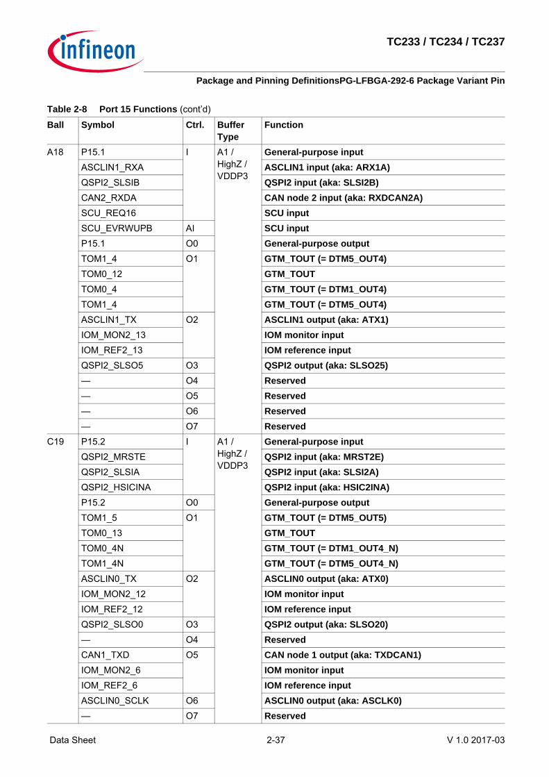
A18 P15.1 I A1 / HighZ / VDDP3
General-purpose inputASCLIN1_RXA ASCLIN1 input (aka: ARX1A)QSPI2_SLSIB QSPI2 input (aka: SLSI2B)CAN2_RXDA CAN node 2 input (aka: RXDCAN2A)SCU_REQ16 SCU inputSCU_EVRWUPB AI SCU inputP15.1 O0 General-purpose outputTOM1_4 O1 GTM_TOUT (= DTM5_OUT4)TOM0_12 GTM_TOUTTOM0_4 GTM_TOUT (= DTM1_OUT4)TOM1_4 GTM_TOUT (= DTM5_OUT4)ASCLIN1_TX O2 ASCLIN1 output (aka: ATX1)IOM_MON2_13 IOM monitor inputIOM_REF2_13 IOM reference inputQSPI2_SLSO5 O3 QSPI2 output (aka: SLSO25)— O4 Reserved— O5 Reserved— O6 Reserved— O7 Reserved
C19 P15.2 I A1 / HighZ / VDDP3
General-purpose inputQSPI2_MRSTE QSPI2 input (aka: MRST2E)QSPI2_SLSIA QSPI2 input (aka: SLSI2A)QSPI2_HSICINA QSPI2 input (aka: HSIC2INA)P15.2 O0 General-purpose outputTOM1_5 O1 GTM_TOUT (= DTM5_OUT5)TOM0_13 GTM_TOUTTOM0_4N GTM_TOUT (= DTM1_OUT4_N)TOM1_4N GTM_TOUT (= DTM5_OUT4_N)ASCLIN0_TX O2 ASCLIN0 output (aka: ATX0)IOM_MON2_12 IOM monitor inputIOM_REF2_12 IOM reference inputQSPI2_SLSO0 O3 QSPI2 output (aka: SLSO20)— O4 ReservedCAN1_TXD O5 CAN node 1 output (aka: TXDCAN1)IOM_MON2_6 IOM monitor inputIOM_REF2_6 IOM reference inputASCLIN0_SCLK O6 ASCLIN0 output (aka: ASCLK0)— O7 Reserved
Table 2-8 Port 15 Functions (cont’d)
Ball Symbol Ctrl. Buffer Type
Function

TC233 / TC234 / TC237
Package and Pinning DefinitionsPG-LFBGA-292-6 Package Variant Pin
Data Sheet 2-38 V 1.0 2017-03
B17 P15.3 I A1 / HighZ / VDDP3
General-purpose inputASCLIN0_RXB ASCLIN0 input (aka: ARX0B)QSPI2_SCLKA QSPI2 input (aka: SCLK2A)QSPI2_HSICINB QSPI2 input (aka: HSIC2INB)CAN1_RXDA CAN node 1 input (aka: RXDCAN1A)P15.3 O0 General-purpose outputTOM1_6 O1 GTM_TOUT (= DTM5_OUT6)TOM0_14 GTM_TOUTTOM0_5 GTM_TOUT (= DTM1_OUT5)TOM1_5 GTM_TOUT (= DTM5_OUT5)ASCLIN0_TX O2 ASCLIN0 output (aka: ATX0)IOM_MON2_12 IOM monitor inputIOM_REF2_12 IOM reference inputQSPI2_SCLK O3 QSPI2 output (aka: SCLK2)— O4 Reserved— O5 Reserved— O6 Reserved— O7 Reserved
A17 P15.4 I A1 / HighZ / VDDP3
General-purpose inputQSPI2_MRSTA QSPI2 input (aka: MRST2A)SCU_REQ0 SCU inputP15.4 O0 General-purpose outputTOM1_7 O1 GTM_TOUT (= DTM5_OUT7)TOM0_15 GTM_TOUTASCLIN1_TX O2 ASCLIN1 output (aka: ATX1)IOM_MON2_13 IOM monitor inputIOM_REF2_13 IOM reference inputQSPI2_MRST O3 QSPI2 output (aka: MRST2)IOM_MON2_2 IOM monitor inputIOM_REF2_2 IOM reference input— O4 Reserved— O5 Reserved— O6 ReservedCCU60_CC62 O7 CCU60 outputIOM_MON1_0 IOM monitor inputIOM_REF1_4 IOM reference input
Table 2-8 Port 15 Functions (cont’d)
Ball Symbol Ctrl. Buffer Type
Function
TC233 / TC234 / TC237
Package and Pinning DefinitionsPG-LFBGA-292-6 Package Variant Pin
Data Sheet 2-39 V 1.0 2017-03
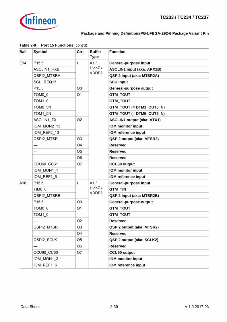
E14 P15.5 I A1 / HighZ / VDDP3
General-purpose inputASCLIN1_RXB ASCLIN1 input (aka: ARX1B)QSPI2_MTSRA QSPI2 input (aka: MTSR2A)SCU_REQ13 SCU inputP15.5 O0 General-purpose outputTOM0_0 O1 GTM_TOUTTOM1_0 GTM_TOUTTOM0_5N GTM_TOUT (= DTM1_OUT5_N)TOM1_5N GTM_TOUT (= DTM5_OUT5_N)ASCLIN1_TX O2 ASCLIN1 output (aka: ATX1)IOM_MON2_13 IOM monitor inputIOM_REF2_13 IOM reference inputQSPI2_MTSR O3 QSPI2 output (aka: MTSR2)— O4 Reserved— O5 Reserved— O6 ReservedCCU60_CC61 O7 CCU60 outputIOM_MON1_1 IOM monitor inputIOM_REF1_5 IOM reference input
A16 P15.6 I A1 / HighZ / VDDP3
General-purpose inputTIM0_0 GTM_TINQSPI2_MTSRB QSPI2 input (aka: MTSR2B)P15.6 O0 General-purpose outputTOM0_0 O1 GTM_TOUTTOM1_0 GTM_TOUT— O2 ReservedQSPI2_MTSR O3 QSPI2 output (aka: MTSR2)— O4 ReservedQSPI2_SCLK O5 QSPI2 output (aka: SCLK2)— O6 ReservedCCU60_CC60 O7 CCU60 outputIOM_MON1_2 IOM monitor inputIOM_REF1_6 IOM reference input
Table 2-8 Port 15 Functions (cont’d)
Ball Symbol Ctrl. Buffer Type
Function

TC233 / TC234 / TC237
Package and Pinning DefinitionsPG-LFBGA-292-6 Package Variant Pin
Data Sheet 2-40 V 1.0 2017-03
D15 P15.7 I A1 / HighZ / VDDP3
General-purpose inputTIM0_1 GTM_TINQSPI2_MRSTB QSPI2 input (aka: MRST2B)P15.7 O0 General-purpose outputTOM0_1 O1 GTM_TOUTTOM1_1 GTM_TOUT— O2 ReservedQSPI2_MRST O3 QSPI2 output (aka: MRST2)IOM_MON2_2 IOM monitor inputIOM_REF2_2 IOM reference input— O4 Reserved— O5 Reserved— O6 ReservedCCU60_COUT60 O7 CCU60 outputIOM_MON1_3 IOM monitor inputIOM_REF1_3 IOM reference input
D14 P15.8 I A1 / HighZ / VDDP3
General-purpose inputTIM0_2 GTM_TINQSPI2_SCLKB QSPI2 input (aka: SCLK2B)SCU_REQ1 SCU inputP15.8 O0 General-purpose outputTOM0_2 O1 GTM_TOUTTOM1_2 GTM_TOUT— O2 ReservedQSPI2_SCLK O3 QSPI2 output (aka: SCLK2)— O4 Reserved— O5 Reserved— O6 ReservedCCU60_COUT61 O7 CCU60 outputIOM_MON1_4 IOM monitor inputIOM_REF1_2 IOM reference input
Table 2-8 Port 15 Functions (cont’d)
Ball Symbol Ctrl. Buffer Type
Function

TC233 / TC234 / TC237
Package and Pinning DefinitionsPG-LFBGA-292-6 Package Variant Pin
Data Sheet 2-41 V 1.0 2017-03
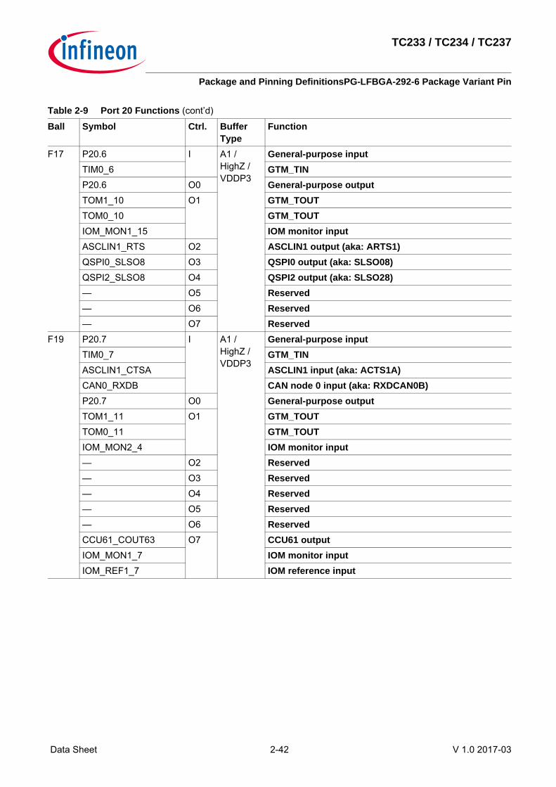
Table 2-9 Port 20 FunctionsBall Symbol Ctrl. Buffer
TypeFunction
H20 P20.0 I A1 / HighZ / VDDP3
General-purpose inputTIM0_6 GTM_TINSCU_REQ9 SCU inputOCDS_TGI0 OCDS inputGPT120_T6EUDA GPT120 inputCAN11_RXDC CAN1 node 1 input (aka: RXDCAN11C)CAN12_RXDC CAN1 node 2 input (aka: RXDCAN12C)P20.0 O0 General-purpose outputTOM0_6 O1 GTM_TOUT (= DTM1_OUT6)TOM1_6 GTM_TOUT (= DTM5_OUT6)— O2 Reserved— O3 Reserved— O4 Reserved— O5 Reserved— O6 Reserved— O7 ReservedOCDS_TGO0 O OCDS
H19 P20.2 I Input Only / PU / VDDP3
General-purpose inputTESTMODE Factory Test Mode Enable
G20 P20.3 I A1 / HighZ / VDDP3
General-purpose inputTIM0_4 GTM_TINGPT120_T6INA GPT120 inputP20.3 O0 General-purpose outputTOM1_12 O1 GTM_TOUTTOM0_4 GTM_TOUT (= DTM1_OUT4)IOM_MON1_14 IOM monitor input— O2 ReservedQSPI0_SLSO9 O3 QSPI0 output (aka: SLSO09)QSPI2_SLSO9 O4 QSPI2 output (aka: SLSO29)CAN12_TXD O5 CAN1 node 2 output (aka: TXDCAN12)— O6 Reserved— O7 Reserved
TC233 / TC234 / TC237
Package and Pinning DefinitionsPG-LFBGA-292-6 Package Variant Pin
Data Sheet 2-42 V 1.0 2017-03
F17 P20.6 I A1 / HighZ / VDDP3
General-purpose inputTIM0_6 GTM_TINP20.6 O0 General-purpose outputTOM1_10 O1 GTM_TOUTTOM0_10 GTM_TOUTIOM_MON1_15 IOM monitor inputASCLIN1_RTS O2 ASCLIN1 output (aka: ARTS1)QSPI0_SLSO8 O3 QSPI0 output (aka: SLSO08)QSPI2_SLSO8 O4 QSPI2 output (aka: SLSO28)— O5 Reserved— O6 Reserved— O7 Reserved
F19 P20.7 I A1 / HighZ / VDDP3
General-purpose inputTIM0_7 GTM_TINASCLIN1_CTSA ASCLIN1 input (aka: ACTS1A)CAN0_RXDB CAN node 0 input (aka: RXDCAN0B)P20.7 O0 General-purpose outputTOM1_11 O1 GTM_TOUTTOM0_11 GTM_TOUTIOM_MON2_4 IOM monitor input— O2 Reserved— O3 Reserved— O4 Reserved— O5 Reserved— O6 ReservedCCU61_COUT63 O7 CCU61 outputIOM_MON1_7 IOM monitor inputIOM_REF1_7 IOM reference input
Table 2-9 Port 20 Functions (cont’d)
Ball Symbol Ctrl. Buffer Type
Function

TC233 / TC234 / TC237
Package and Pinning DefinitionsPG-LFBGA-292-6 Package Variant Pin
Data Sheet 2-43 V 1.0 2017-03
F20 P20.8 I A1 / HighZ / VDDP3
General-purpose inputTIM0_7 GTM_TINP20.8 O0 General-purpose outputTOM1_7 O1 GTM_TOUT (= DTM5_OUT7)TOM0_7 GTM_TOUT (= DTM1_OUT7)TOM0_4 GTM_TOUT (= DTM1_OUT4)TOM1_4 GTM_TOUT (= DTM5_OUT4)IOM_MON2_8 IOM monitor inputASCLIN1_SLSO O2 ASCLIN1 output (aka: ASLSO1)QSPI0_SLSO0 O3 QSPI0 output (aka: SLSO00)QSPI1_SLSO0 O4 QSPI1 output (aka: SLSO10)CAN0_TXD O5 CAN node 0 output (aka: TXDCAN0)IOM_MON2_5 IOM monitor inputIOM_REF2_5 IOM reference inputSCU_WDT0LCK O6 SCU outputCCU61_CC60 O7 CCU61 outputIOM_MON1_8 IOM monitor inputIOM_REF1_13 IOM reference input
E17 P20.9 I A1 / HighZ / VDDP3
General-purpose inputASCLIN1_RXC ASCLIN1 input (aka: ARX1C)QSPI0_SLSIB QSPI0 input (aka: SLSI0B)SCU_REQ11 SCU inputCAN12_RXDE CAN1 node 2 input (aka: RXDCAN12E)P20.9 O0 General-purpose outputTOM1_13 O1 GTM_TOUTTOM0_13 GTM_TOUTTOM0_4N GTM_TOUT (= DTM1_OUT4_N)TOM1_4N GTM_TOUT (= DTM5_OUT4_N)IOM_MON2_11 IOM monitor input— O2 ReservedQSPI0_SLSO1 O3 QSPI0 output (aka: SLSO01)QSPI1_SLSO1 O4 QSPI1 output (aka: SLSO11)— O5 ReservedSCU_WDTSLCK O6 SCU outputCCU61_CC61 O7 CCU61 outputIOM_MON1_9 IOM monitor inputIOM_REF1_12 IOM reference input
Table 2-9 Port 20 Functions (cont’d)
Ball Symbol Ctrl. Buffer Type
Function

TC233 / TC234 / TC237
Package and Pinning DefinitionsPG-LFBGA-292-6 Package Variant Pin
Data Sheet 2-44 V 1.0 2017-03
E19 P20.10 I A1 / HighZ / VDDP3
General-purpose inputP20.10 O0 General-purpose outputTOM1_14 O1 GTM_TOUTTOM0_14 GTM_TOUTTOM0_5 GTM_TOUT (= DTM1_OUT5)TOM1_5 GTM_TOUT (= DTM5_OUT5)IOM_MON2_14 IOM monitor inputASCLIN1_TX O2 ASCLIN1 output (aka: ATX1)IOM_MON2_13 IOM monitor inputIOM_REF2_13 IOM reference inputQSPI0_SLSO6 O3 QSPI0 output (aka: SLSO06)QSPI2_SLSO7 O4 QSPI2 output (aka: SLSO27)CAN12_TXD O5 CAN1 node 2 output (aka: TXDCAN12)ASCLIN1_SCLK O6 ASCLIN1 output (aka: ASCLK1)CCU61_CC62 O7 CCU61 outputIOM_MON1_10 IOM monitor inputIOM_REF1_11 IOM reference input
E20 P20.11 I A1+ / HighZ / VDDP3
General-purpose inputQSPI0_SCLKA QSPI0 input (aka: SCLK0A)P20.11 O0 General-purpose outputTOM1_15 O1 GTM_TOUTTOM0_15 GTM_TOUTTOM0_5N GTM_TOUT (= DTM1_OUT5_N)TOM1_5N GTM_TOUT (= DTM5_OUT5_N)IOM_MON2_15 IOM monitor input— O2 ReservedQSPI0_SCLK O3 QSPI0 output (aka: SCLK0)— O4 ReservedCAN11_TXD O5 CAN1 node 1 output (aka: TXDCAN11)— O6 ReservedCCU61_COUT60 O7 CCU61 outputIOM_MON1_11 IOM monitor inputIOM_REF1_10 IOM reference input
Table 2-9 Port 20 Functions (cont’d)
Ball Symbol Ctrl. Buffer Type
Function

TC233 / TC234 / TC237
Package and Pinning DefinitionsPG-LFBGA-292-6 Package Variant Pin
Data Sheet 2-45 V 1.0 2017-03
D19 P20.12 I A1 / HighZ / VDDP3
General-purpose inputQSPI0_MRSTA QSPI0 input (aka: MRST0A)CAN11_RXDH CAN1 node 1 input (aka: RXDCAN11H)IOM_PIN13 IOM pad inputP20.12 O0 General-purpose outputTOM1_0 O1 GTM_TOUTTOM0_8 GTM_TOUTTOM0_6 GTM_TOUT (= DTM1_OUT6)TOM1_6 GTM_TOUT (= DTM5_OUT6)IOM_MON0_13 IOM monitor input— O2 ReservedQSPI0_MRST O3 QSPI0 output (aka: MRST0)IOM_MON2_0 IOM monitor inputIOM_REF2_0 IOM reference inputQSPI0_MTSR O4 QSPI0 output (aka: MTSR0)— O5 Reserved— O6 ReservedCCU61_COUT61 O7 CCU61 outputIOM_MON1_12 IOM monitor inputIOM_REF1_9 IOM reference input
D20 P20.13 I A1+ / HighZ / VDDP3
General-purpose inputQSPI0_SLSIA QSPI0 input (aka: SLSI0A)CAN12_RXDH CAN1 node 2 input (aka: RXDCAN12H)IOM_PIN14 IOM pad inputP20.13 O0 General-purpose outputTOM1_1 O1 GTM_TOUTTOM0_9 GTM_TOUTTOM0_6N GTM_TOUT (= DTM1_OUT6_N)TOM1_6N GTM_TOUT (= DTM5_OUT6_N)IOM_MON0_14 IOM monitor input— O2 ReservedQSPI0_SLSO2 O3 QSPI0 output (aka: SLSO02)QSPI1_SLSO2 O4 QSPI1 output (aka: SLSO12)QSPI0_SCLK O5 QSPI0 output (aka: SCLK0)— O6 ReservedCCU61_COUT62 O7 CCU61 outputIOM_MON1_13 IOM monitor inputIOM_REF1_8 IOM reference input
Table 2-9 Port 20 Functions (cont’d)
Ball Symbol Ctrl. Buffer Type
Function

TC233 / TC234 / TC237
Package and Pinning DefinitionsPG-LFBGA-292-6 Package Variant Pin
Data Sheet 2-46 V 1.0 2017-03
C20 P20.14 I A1+ / HighZ / VDDP3
General-purpose inputQSPI0_MTSRA QSPI0 input (aka: MTSR0A)IOM_PIN15 IOM pad inputP20.14 O0 General-purpose outputTOM1_2 O1 GTM_TOUTTOM0_10 GTM_TOUTTOM0_7 GTM_TOUT (= DTM1_OUT7)TOM1_7 GTM_TOUT (= DTM5_OUT7)IOM_MON0_15 IOM monitor input— O2 ReservedQSPI0_MTSR O3 QSPI0 output (aka: MTSR0)— O4 ReservedCAN12_TXD O5 CAN1 node 2 output (aka: TXDCAN12)— O6 Reserved— O7 Reserved
Table 2-10 Port 21 FunctionsBall Symbol Ctrl. Buffer
TypeFunction
K19 P21.2 I A1 / HighZ / VDDP3
General-purpose inputTIM0_0 GTM_TINSCU_EMGSTOPB SCU inputP21.2 O0 General-purpose outputTOM0_0 O1 GTM_TOUTTOM1_0 GTM_TOUTTOM0_4 GTM_TOUT (= DTM1_OUT4)TOM1_4 GTM_TOUT (= DTM5_OUT4)— O2 Reserved— O3 Reserved— O4 Reserved— O5 Reserved— O6 Reserved— O7 Reserved
Table 2-9 Port 20 Functions (cont’d)
Ball Symbol Ctrl. Buffer Type
Function

TC233 / TC234 / TC237
Package and Pinning DefinitionsPG-LFBGA-292-6 Package Variant Pin
Data Sheet 2-47 V 1.0 2017-03
J19 P21.3 I A1 / HighZ / VDDP3
General-purpose inputTIM0_1 GTM_TINP21.3 O0 General-purpose outputTOM0_1 O1 GTM_TOUTTOM1_1 GTM_TOUTTOM0_4N GTM_TOUT (= DTM1_OUT4_N)TOM1_4N GTM_TOUT (= DTM5_OUT4_N)— O2 Reserved— O3 Reserved— O4 Reserved— O5 Reserved— O6 Reserved— O7 Reserved
K20 P21.4 I A1 / HighZ / VDDP3
General-purpose inputTIM0_2 GTM_TINP21.4 O0 General-purpose outputTOM0_2 O1 GTM_TOUTTOM1_2 GTM_TOUTTOM0_5 GTM_TOUT (= DTM1_OUT5)TOM1_5 GTM_TOUT (= DTM5_OUT5)— O2 Reserved— O3 Reserved— O4 Reserved— O5 Reserved— O6 Reserved— O7 Reserved
Table 2-10 Port 21 Functions (cont’d)
Ball Symbol Ctrl. Buffer Type
Function

TC233 / TC234 / TC237
Package and Pinning DefinitionsPG-LFBGA-292-6 Package Variant Pin
Data Sheet 2-48 V 1.0 2017-03
J20 P21.5 I A1 / HighZ / VDDP3
General-purpose inputTIM0_3 GTM_TINP21.5 O0 General-purpose outputTOM0_3 O1 GTM_TOUTTOM1_3 GTM_TOUTTOM0_5N GTM_TOUT (= DTM1_OUT5_N)TOM1_5N GTM_TOUT (= DTM5_OUT5_N)— O2 Reserved— O3 Reserved— O4 Reserved— O5 Reserved— O6 Reserved— O7 Reserved
H17 P21.6 I A1 / PU / VDDP3
General-purpose inputTIM0_4 GTM_TINTDI OCDS inputOCDS_TGI2 OCDS inputGPT120_T5EUDA GPT120 inputP21.6 O0 General-purpose outputTOM0_4 O1 GTM_TOUT (= DTM1_OUT4)TOM1_4 GTM_TOUT (= DTM5_OUT4)— O2 Reserved— O3 Reserved— O4 Reserved— O5 Reserved— O6 ReservedGPT120_T3OUT O7 GPT120 outputOCDS_TGO2 O OCDS
Table 2-10 Port 21 Functions (cont’d)
Ball Symbol Ctrl. Buffer Type
Function

TC233 / TC234 / TC237
Package and Pinning DefinitionsPG-LFBGA-292-6 Package Variant Pin
Data Sheet 2-49 V 1.0 2017-03
H16 P21.7 I A1+ / PU / VDDP3
General-purpose inputTIM0_5 GTM_TINOCDS_DAP2 OCDS inputOCDS_TGI3 OCDS inputGPT120_T5INA GPT120 inputP21.7 O0 General-purpose outputTOM0_5 O1 GTM_TOUT (= DTM1_OUT5)TOM1_5 GTM_TOUT (= DTM5_OUT5)— O2 Reserved— O3 Reserved— O4 Reserved— O5 Reserved— O6 ReservedGPT120_T6OUT O7 GPT120 outputOCDS_TGO3 O OCDSOCDS_DAP2 O OCDS OutputTDO O JTAG Output
Table 2-11 Port 22 FunctionsBall Symbol Ctrl. Buffer
TypeFunction
P20 P22.0 I A1 / HighZ / VDDP3
General-purpose inputTIM0_1 GTM_TINQSPI3_MTSRE QSPI3 input (aka: MTSR3E)P22.0 O0 General-purpose outputTOM0_9 O1 GTM_TOUTTOM1_1 GTM_TOUT— O2 ReservedQSPI3_MTSR O3 QSPI3 output (aka: MTSR3)— O4 Reserved— O5 Reserved— O6 Reserved— O7 Reserved
Table 2-10 Port 21 Functions (cont’d)
Ball Symbol Ctrl. Buffer Type
Function

TC233 / TC234 / TC237
Package and Pinning DefinitionsPG-LFBGA-292-6 Package Variant Pin
Data Sheet 2-50 V 1.0 2017-03
P19 P22.1 I A1 / HighZ / VDDP3
General-purpose inputTIM0_0 GTM_TINQSPI3_MRSTE QSPI3 input (aka: MRST3E)P22.1 O0 General-purpose outputTOM0_8 O1 GTM_TOUTTOM1_0 GTM_TOUTTOM0_6 GTM_TOUT (= DTM1_OUT6)TOM1_6 GTM_TOUT (= DTM5_OUT6)— O2 ReservedQSPI3_MRST O3 QSPI3 output (aka: MRST3)IOM_MON2_3 IOM monitor inputIOM_REF2_3 IOM reference input— O4 Reserved— O5 Reserved— O6 Reserved— O7 Reserved
R20 P22.2 I A1 / HighZ / VDDP3
General-purpose inputTIM0_3 GTM_TINQSPI3_SLSID QSPI3 input (aka: SLSI3D)P22.2 O0 General-purpose outputTOM0_11 O1 GTM_TOUTTOM1_3 GTM_TOUTTOM0_6N GTM_TOUT (= DTM1_OUT6_N)TOM1_6N GTM_TOUT (= DTM5_OUT6_N)— O2 ReservedQSPI3_SLSO12 O3 QSPI3 output (aka: SLSO312)— O4 Reserved— O5 Reserved— O6 Reserved— O7 Reserved
Table 2-11 Port 22 Functions (cont’d)
Ball Symbol Ctrl. Buffer Type
Function

TC233 / TC234 / TC237
Package and Pinning DefinitionsPG-LFBGA-292-6 Package Variant Pin
Data Sheet 2-51 V 1.0 2017-03
R19 P22.3 I A1 / HighZ / VDDP3
General-purpose inputTIM0_4 GTM_TINQSPI3_SCLKE QSPI3 input (aka: SCLK3E)P22.3 O0 General-purpose outputTOM0_12 O1 GTM_TOUTTOM1_4 GTM_TOUT (= DTM5_OUT4)TOM0_7 GTM_TOUT (= DTM1_OUT7)TOM1_7 GTM_TOUT (= DTM5_OUT7)— O2 ReservedQSPI3_SCLK O3 QSPI3 output (aka: SCLK3)— O4 Reserved— O5 Reserved— O6 Reserved— O7 Reserved
P16 P22.4 I A1 / HighZ / VDDP3
General-purpose inputP22.4 O0 General-purpose outputTOM0_7N O1 GTM_TOUT (= DTM1_OUT7_N)TOM1_7N GTM_TOUT (= DTM5_OUT7_N)— O2 Reserved— O3 ReservedQSPI0_SLSO12 O4 QSPI0 output (aka: SLSO012)— O5 Reserved— O6 Reserved— O7 Reserved
Table 2-11 Port 22 Functions (cont’d)
Ball Symbol Ctrl. Buffer Type
Function

TC233 / TC234 / TC237
Package and Pinning DefinitionsPG-LFBGA-292-6 Package Variant Pin
Data Sheet 2-52 V 1.0 2017-03
Table 2-12 Port 23 FunctionsBall Symbol Ctrl. Buffer
TypeFunction
U19 P23.1 I A1+ / HighZ / VDDP3
General-purpose inputTIM0_6 GTM_TINP23.1 O0 General-purpose outputTOM0_6 O1 GTM_TOUT (= DTM1_OUT6)TOM0_15 GTM_TOUTASCLIN1_RTS O2 ASCLIN1 output (aka: ARTS1)QSPI3_SLSO13 O3 QSPI3 output (aka: SLSO313)GTM_CLK0 O4 GTM outputSCU_EXTCLK1 O5 SCU outputSCU_EXTCLK0 O6 SCU output— O7 Reserved
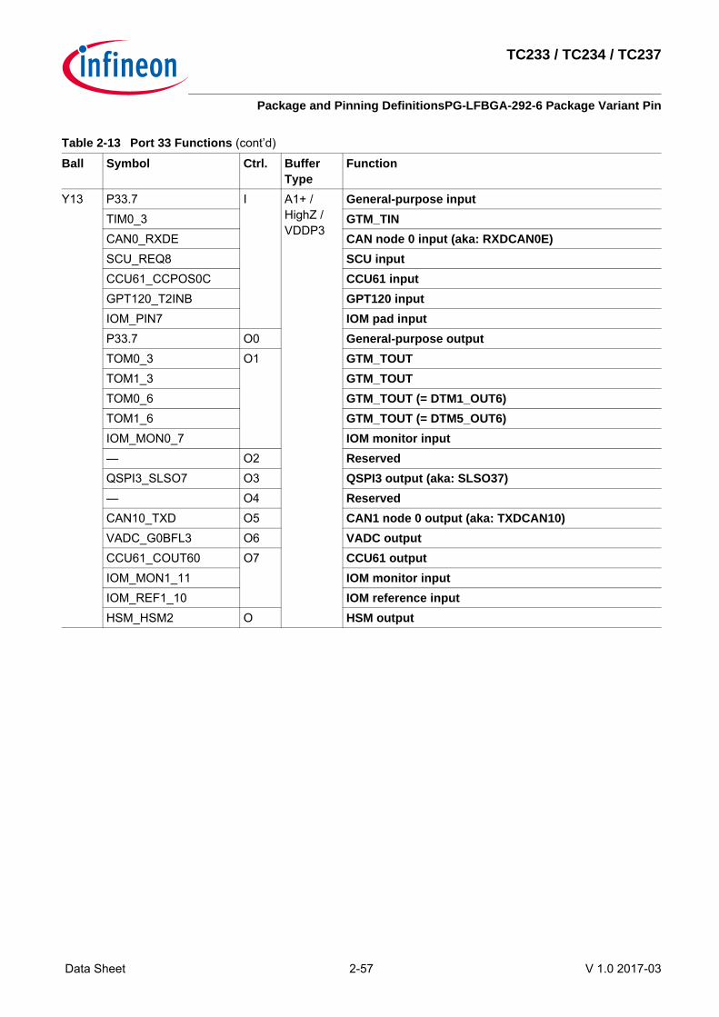
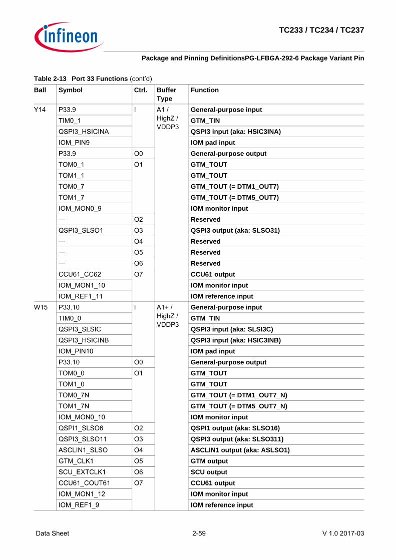
Table 2-13 Port 33 FunctionsBall Symbol Ctrl. Buffer
TypeFunction
W10 P33.0 I A1 / HighZ / VDDP3
General-purpose inputTIM0_4 GTM_TINIOM_PIN0 IOM pad inputP33.0 O0 General-purpose outputTOM0_4 O1 GTM_TOUT (= DTM1_OUT4)TOM1_4 GTM_TOUT (= DTM5_OUT4)IOM_MON0_0 IOM monitor input— O2 Reserved— O3 Reserved— O4 Reserved— O5 ReservedVADC_G1BFL0 O6 VADC output— O7 Reserved

TC233 / TC234 / TC237
Package and Pinning DefinitionsPG-LFBGA-292-6 Package Variant Pin
Data Sheet 2-53 V 1.0 2017-03
Y10 P33.1 I A1 / HighZ / VDDP3
General-purpose inputTIM0_5 GTM_TINIOM_PIN1 IOM pad inputP33.1 O0 General-purpose outputTOM0_5 O1 GTM_TOUT (= DTM1_OUT5)TOM1_5 GTM_TOUT (= DTM5_OUT5)IOM_MON0_1 IOM monitor input— O2 Reserved— O3 Reserved— O4 ReservedVADC_EMUX02 O5 VADC outputVADC_G1BFL1 O6 VADC output— O7 Reserved
W11 P33.2 I A1 / HighZ / VDDP3
General-purpose inputTIM0_6 GTM_TINIOM_PIN2 IOM pad inputP33.2 O0 General-purpose outputTOM0_6 O1 GTM_TOUT (= DTM1_OUT6)TOM1_6 GTM_TOUT (= DTM5_OUT6)IOM_MON0_2 IOM monitor input— O2 Reserved— O3 Reserved— O4 ReservedVADC_EMUX01 O5 VADC outputVADC_G1BFL2 O6 VADC outputCCU61_COUT63 O7 CCU61 outputIOM_MON1_7 IOM monitor inputIOM_REF1_7 IOM reference input
Table 2-13 Port 33 Functions (cont’d)
Ball Symbol Ctrl. Buffer Type
Function

TC233 / TC234 / TC237
Package and Pinning DefinitionsPG-LFBGA-292-6 Package Variant Pin
Data Sheet 2-54 V 1.0 2017-03
Y11 P33.3 I A1 / HighZ / VDDP3
General-purpose inputTIM0_7 GTM_TINIOM_PIN3 IOM pad inputP33.3 O0 General-purpose outputTOM0_7 O1 GTM_TOUT (= DTM1_OUT7)TOM1_7 GTM_TOUT (= DTM5_OUT7)IOM_MON0_3 IOM monitor input— O2 Reserved— O3 Reserved— O4 ReservedVADC_EMUX00 O5 VADC outputVADC_G1BFL3 O6 VADC outputCCU61_CC60 O7 CCU61 outputIOM_MON1_8 IOM monitor inputIOM_REF1_13 IOM reference input
W12 P33.4 I A1 / HighZ / VDDP3
General-purpose inputTIM0_0 GTM_TINCCU61_CTRAPC CCU61 inputIOM_PIN4 IOM pad inputP33.4 O0 General-purpose outputTOM0_0 O1 GTM_TOUTTOM1_0 GTM_TOUTIOM_MON0_4 IOM monitor input— O2 Reserved— O3 Reserved— O4 ReservedVADC_EMUX12 O5 VADC outputVADC_G0BFL0 O6 VADC output— O7 Reserved
Table 2-13 Port 33 Functions (cont’d)
Ball Symbol Ctrl. Buffer Type
Function

TC233 / TC234 / TC237
Package and Pinning DefinitionsPG-LFBGA-292-6 Package Variant Pin
Data Sheet 2-55 V 1.0 2017-03
Y12 P33.5 I A1 / HighZ / VDDP3
General-purpose inputTIM0_1 GTM_TINCCU61_CCPOS2C CCU61 inputGPT120_T4EUDB GPT120 inputIOM_PIN5 IOM pad inputP33.5 O0 General-purpose outputTOM0_1 O1 GTM_TOUTTOM1_1 GTM_TOUTTOM0_5 GTM_TOUT (= DTM1_OUT5)TOM1_5 GTM_TOUT (= DTM5_OUT5)IOM_MON0_5 IOM monitor inputQSPI0_SLSO7 O2 QSPI0 output (aka: SLSO07)QSPI1_SLSO7 O3 QSPI1 output (aka: SLSO17)— O4 ReservedVADC_EMUX11 O5 VADC outputVADC_G0BFL1 O6 VADC outputCCU61_CC60 O7 CCU61 outputIOM_MON1_8 IOM monitor inputIOM_REF1_13 IOM reference input
Table 2-13 Port 33 Functions (cont’d)
Ball Symbol Ctrl. Buffer Type
Function

TC233 / TC234 / TC237
Package and Pinning DefinitionsPG-LFBGA-292-6 Package Variant Pin
Data Sheet 2-56 V 1.0 2017-03
W13 P33.6 I A1 / HighZ / VDDP3
General-purpose inputTIM0_2 GTM_TINASCLIN1_RXF ASCLIN1 input (aka: ARX1F)CCU61_CCPOS1C CCU61 inputGPT120_T2EUDB GPT120 inputCAN10_RXDH CAN1 node 0 input (aka: RXDCAN10H)IOM_PIN6 IOM pad inputP33.6 O0 General-purpose outputTOM0_2 O1 GTM_TOUTTOM1_2 GTM_TOUTTOM0_5N GTM_TOUT (= DTM1_OUT5_N)TOM1_5N GTM_TOUT (= DTM5_OUT5_N)IOM_MON0_6 IOM monitor input— O2 Reserved— O3 ReservedASCLIN1_TX O4 ASCLIN1 output (aka: ATX1)IOM_MON2_13 IOM monitor inputIOM_REF2_13 IOM reference inputVADC_EMUX10 O5 VADC outputVADC_G0BFL2 O6 VADC outputCCU61_CC61 O7 CCU61 outputIOM_MON1_9 IOM monitor inputIOM_REF1_12 IOM reference inputHSM_HSM1 O HSM output
Table 2-13 Port 33 Functions (cont’d)
Ball Symbol Ctrl. Buffer Type
Function
TC233 / TC234 / TC237
Package and Pinning DefinitionsPG-LFBGA-292-6 Package Variant Pin
Data Sheet 2-57 V 1.0 2017-03
Y13 P33.7 I A1+ / HighZ / VDDP3
General-purpose inputTIM0_3 GTM_TINCAN0_RXDE CAN node 0 input (aka: RXDCAN0E)SCU_REQ8 SCU inputCCU61_CCPOS0C CCU61 inputGPT120_T2INB GPT120 inputIOM_PIN7 IOM pad inputP33.7 O0 General-purpose outputTOM0_3 O1 GTM_TOUTTOM1_3 GTM_TOUTTOM0_6 GTM_TOUT (= DTM1_OUT6)TOM1_6 GTM_TOUT (= DTM5_OUT6)IOM_MON0_7 IOM monitor input— O2 ReservedQSPI3_SLSO7 O3 QSPI3 output (aka: SLSO37)— O4 ReservedCAN10_TXD O5 CAN1 node 0 output (aka: TXDCAN10)VADC_G0BFL3 O6 VADC outputCCU61_COUT60 O7 CCU61 outputIOM_MON1_11 IOM monitor inputIOM_REF1_10 IOM reference inputHSM_HSM2 O HSM output
Table 2-13 Port 33 Functions (cont’d)
Ball Symbol Ctrl. Buffer Type
Function

TC233 / TC234 / TC237
Package and Pinning DefinitionsPG-LFBGA-292-6 Package Variant Pin
Data Sheet 2-58 V 1.0 2017-03
W14 P33.8 I A1+ / HighZ / VDDP3
General-purpose inputTIM0_4 GTM_TINSCU_EMGSTOPA SCU inputIOM_PIN8 IOM pad inputP33.8 O0 General-purpose outputTOM0_4 O1 GTM_TOUT (= DTM1_OUT4)TOM1_4 GTM_TOUT (= DTM5_OUT4)TOM0_6N GTM_TOUT (= DTM1_OUT6_N)TOM1_6N GTM_TOUT (= DTM5_OUT6_N)IOM_MON0_8 IOM monitor input— O2 ReservedQSPI3_SLSO2 O3 QSPI3 output (aka: SLSO32)— O4 ReservedCAN0_TXD O5 CAN node 0 output (aka: TXDCAN0)IOM_MON2_5 IOM monitor inputIOM_REF2_5 IOM reference input— O6 ReservedCCU61_COUT62 O7 CCU61 outputIOM_MON1_13 IOM monitor inputIOM_REF1_8 IOM reference inputSMU_FSP O SMU
Table 2-13 Port 33 Functions (cont’d)
Ball Symbol Ctrl. Buffer Type
Function
TC233 / TC234 / TC237
Package and Pinning DefinitionsPG-LFBGA-292-6 Package Variant Pin
Data Sheet 2-59 V 1.0 2017-03
Y14 P33.9 I A1 / HighZ / VDDP3
General-purpose inputTIM0_1 GTM_TINQSPI3_HSICINA QSPI3 input (aka: HSIC3INA)IOM_PIN9 IOM pad inputP33.9 O0 General-purpose outputTOM0_1 O1 GTM_TOUTTOM1_1 GTM_TOUTTOM0_7 GTM_TOUT (= DTM1_OUT7)TOM1_7 GTM_TOUT (= DTM5_OUT7)IOM_MON0_9 IOM monitor input— O2 ReservedQSPI3_SLSO1 O3 QSPI3 output (aka: SLSO31)— O4 Reserved— O5 Reserved— O6 ReservedCCU61_CC62 O7 CCU61 outputIOM_MON1_10 IOM monitor inputIOM_REF1_11 IOM reference input
W15 P33.10 I A1+ / HighZ / VDDP3
General-purpose inputTIM0_0 GTM_TINQSPI3_SLSIC QSPI3 input (aka: SLSI3C)QSPI3_HSICINB QSPI3 input (aka: HSIC3INB)IOM_PIN10 IOM pad inputP33.10 O0 General-purpose outputTOM0_0 O1 GTM_TOUTTOM1_0 GTM_TOUTTOM0_7N GTM_TOUT (= DTM1_OUT7_N)TOM1_7N GTM_TOUT (= DTM5_OUT7_N)IOM_MON0_10 IOM monitor inputQSPI1_SLSO6 O2 QSPI1 output (aka: SLSO16)QSPI3_SLSO11 O3 QSPI3 output (aka: SLSO311)ASCLIN1_SLSO O4 ASCLIN1 output (aka: ASLSO1)GTM_CLK1 O5 GTM outputSCU_EXTCLK1 O6 SCU outputCCU61_COUT61 O7 CCU61 outputIOM_MON1_12 IOM monitor inputIOM_REF1_9 IOM reference input
Table 2-13 Port 33 Functions (cont’d)
Ball Symbol Ctrl. Buffer Type
Function

TC233 / TC234 / TC237
Package and Pinning DefinitionsPG-LFBGA-292-6 Package Variant Pin
Data Sheet 2-60 V 1.0 2017-03
Y15 P33.11 I A1 / HighZ / VDDP3
General-purpose inputTIM0_2 GTM_TINQSPI3_SCLKD QSPI3 input (aka: SCLK3D)SCU_REQ17 SCU inputIOM_PIN11 IOM pad inputP33.11 O0 General-purpose outputTOM0_2 O1 GTM_TOUTTOM1_2 GTM_TOUTIOM_MON0_11 IOM monitor inputASCLIN1_SCLK O2 ASCLIN1 output (aka: ASCLK1)QSPI3_SCLK O3 QSPI3 output (aka: SCLK3)— O4 Reserved— O5 ReservedSMPS_DCDCSYNC O6 SCU outputCCU61_CC61 O7 CCU61 outputIOM_MON1_9 IOM monitor inputIOM_REF1_12 IOM reference inputSMPS_DCDCSYNC O SCU output
W16 P33.12 I A1 / HighZ / VDDP3
General-purpose inputTIM0_0 GTM_TINQSPI3_MTSRD QSPI3 input (aka: MTSR3D)IOM_PIN12 IOM pad inputP33.12 O0 General-purpose outputTOM1_12 O1 GTM_TOUTTOM0_12 GTM_TOUTIOM_MON0_12 IOM monitor inputASCLIN1_TX O2 ASCLIN1 output (aka: ATX1)IOM_MON2_13 IOM monitor inputIOM_REF2_13 IOM reference inputQSPI3_MTSR O3 QSPI3 output (aka: MTSR3)ASCLIN1_SCLK O4 ASCLIN1 output (aka: ASCLK1)— O5 Reserved— O6 ReservedCCU61_COUT60 O7 CCU61 outputIOM_MON1_11 IOM monitor inputIOM_REF1_10 IOM reference input
Table 2-13 Port 33 Functions (cont’d)
Ball Symbol Ctrl. Buffer Type
Function
TC233 / TC234 / TC237
Package and Pinning DefinitionsPG-LFBGA-292-6 Package Variant Pin
Data Sheet 2-61 V 1.0 2017-03
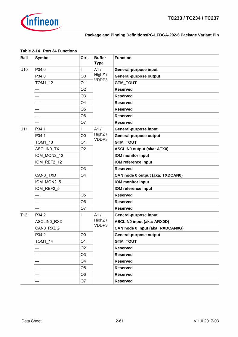
Table 2-14 Port 34 FunctionsBall Symbol Ctrl. Buffer
TypeFunction
U10 P34.0 I A1 / HighZ / VDDP3
General-purpose inputP34.0 O0 General-purpose outputTOM1_12 O1 GTM_TOUT— O2 Reserved— O3 Reserved— O4 Reserved— O5 Reserved— O6 Reserved— O7 Reserved
U11 P34.1 I A1 / HighZ / VDDP3
General-purpose inputP34.1 O0 General-purpose outputTOM1_13 O1 GTM_TOUTASCLIN0_TX O2 ASCLIN0 output (aka: ATX0)IOM_MON2_12 IOM monitor inputIOM_REF2_12 IOM reference input— O3 ReservedCAN0_TXD O4 CAN node 0 output (aka: TXDCAN0)IOM_MON2_5 IOM monitor inputIOM_REF2_5 IOM reference input— O5 Reserved— O6 Reserved— O7 Reserved
T12 P34.2 I A1 / HighZ / VDDP3
General-purpose inputASCLIN0_RXD ASCLIN0 input (aka: ARX0D)CAN0_RXDG CAN node 0 input (aka: RXDCAN0G)P34.2 O0 General-purpose outputTOM1_14 O1 GTM_TOUT— O2 Reserved— O3 Reserved— O4 Reserved— O5 Reserved— O6 Reserved— O7 Reserved

TC233 / TC234 / TC237
Package and Pinning DefinitionsPG-LFBGA-292-6 Package Variant Pin
Data Sheet 2-62 V 1.0 2017-03
U12 P34.3 I A1 / HighZ / VDDP3
General-purpose inputASCLIN1_CTSB ASCLIN1 input (aka: ACTS1B)P34.3 O0 General-purpose outputTOM1_15 O1 GTM_TOUT— O2 Reserved— O3 ReservedQSPI2_SLSO10 O4 QSPI2 output (aka: SLSO210)— O5 Reserved— O6 Reserved— O7 Reserved
Table 2-15 Port 40 FunctionsBall Symbol Ctrl. Buffer
TypeFunction
W9 P40.0 I S / VDDM General-purpose inputVADCG0_0 AI VADC input channel 0 of group 0
Y9 P40.1 I S / VDDM General-purpose inputVADCG0_1 AI VADC input channel 1 of group 0
(with multiplexer diagnostics)W8 P40.2 I S / VDDM General-purpose input
VADCG0_2 AI VADC input channel 2 of group 0(with multiplexer diagnostics)
Y8 P40.3 I S / VDDM General-purpose inputVADCG0_3 AI VADC input channel 3 of group 0
W7 P40.4 I S / VDDM General-purpose inputVADCG0_4 AI VADC input channel 4 of group 0
W6 P40.5 I S / VDDM General-purpose inputVADCG0_5 AI VADC input channel 5 of group 0
W5 P40.6 I S / VDDM General-purpose inputVADCG0_6 AI VADC input channel 6 of group 0
W4 P40.7 I S / VDDM General-purpose inputVADCG0_7 AI VADC input channel 7 of group 0
(with pull down diagnostics)W3 P40.8 I S / VDDM General-purpose input
VADCG0_8 AI VADC input channel 8 of group 0Y3 P40.9 I S / VDDM General-purpose input
VADCG0_9 AI VADC input channel 9 of group 0(with multiplexer diagnostics)
Table 2-14 Port 34 Functions (cont’d)
Ball Symbol Ctrl. Buffer Type
Function

TC233 / TC234 / TC237
Package and Pinning DefinitionsPG-LFBGA-292-6 Package Variant Pin
Data Sheet 2-63 V 1.0 2017-03
Y2 P40.10 I S / VDDM General-purpose inputVADCG0_10 AI VADC input channel 10 of group 0
(with multiplexer diagnostics)W1 P40.11 I S / VDDM General-purpose input
SENT_SENT0A SENT inputCCU60_CCPOS0D CCU60 inputVADCG0_11 AI VADC input channel 11 of group 0
Table 2-16 Port 41 FunctionsBall Symbol Ctrl. Buffer
TypeFunction
V2 P41.0 I S / VDDM General-purpose inputSENT_SENT1A SENT inputCCU60_CCPOS1B CCU60 inputVADCG1_0 AI VADC input channel 0 of group 1
V1 P41.1 I S / VDDM General-purpose inputVADCG1_1 AI VADC input channel 1 of group 1
(with multiplexer diagnostics)U2 P41.2 I S / VDDM General-purpose input
SENT_SENT2A SENT inputCCU61_CCPOS1B CCU61 inputVADCG1_2 AI VADC input channel 2 of group 1
(with multiplexer diagnostics)U1 P41.3 I S / VDDM General-purpose input
SENT_SENT3A SENT inputCCU61_CCPOS1D CCU61 inputVADCG1_3 AI VADC input channel 3 of group 1
(with pull down diagnostics)R1 P41.4 I S / VDDM General-purpose input
VADCG1_4 AI VADC input channel 4 of group 1R2 P41.5 I S / VDDM General-purpose input
VADCG1_5 AI VADC input channel 5 of group 1P2 P41.6 I S / VDDM General-purpose input
VADCG1_6 AI VADC input channel 6 of group 1P1 P41.7 I S / VDDM General-purpose input
VADCG1_7 AI VADC input channel 7 of group 1N1 P41.8 I S / VDDM General-purpose input
VADCG1_8 AI VADC input channel 8 of group 1
Table 2-15 Port 40 Functions (cont’d)
Ball Symbol Ctrl. Buffer Type
Function

TC233 / TC234 / TC237
Package and Pinning DefinitionsPG-LFBGA-292-6 Package Variant Pin
Data Sheet 2-64 V 1.0 2017-03
N2 P41.9 I S / VDDM General-purpose inputVADCG1_9 AI VADC input channel 9 of group 1
(with multiplexer diagnostics)M1 P41.10 I S / VDDM General-purpose input
VADCG1_10 AI VADC input channel 10 of group 1(with multiplexer diagnostics)
M2 P41.11 I S / VDDM General-purpose inputVADCG1_11 AI VADC input channel 11 of group 1
Table 2-17 System I/OBall Symbol Ctrl. Buffer
TypeFunction
M20 XTAL1 I VDDP3 Main Oscillator/PLL/Clock Generator InputM19 XTAL2 O VDDP3 Main Oscillator/PLL/Clock Generator OutputK16 TMS/DAP1 I A1+ / PD /
VDDP3Debug Interface
DAP1 I/O Device Access Port LIne 1L19 TRST I Input Only
/ PD / VDDP3
JTAG Module Reset/Enable Input
J16 TCK/DAP0 I Input Only / PD / VDDP3
OCDS inputDAP0 I Device Access Port LIne 0
G16 ESR1 I/O A1+ / PU / VDDP3
SCU inputEVRWUP I EVR Wakeup Pin
G17 PORST I Input Only / PD / VDDP3
Power On ResetAdditional strong PD in case of power fail.
F16 ESR0 I/O A1+ / OD / VDDP3
SCU input/outputEVRWUP I EVR Wakeup Pin
Table 2-18 SupplyBall Symbol Ctrl. Buffer
TypeFunction
Y7 VAGND I — Negative Analog Reference Voltage 0Y6 VAREF I — Positive Analog Reference Voltage 0
Table 2-16 Port 41 Functions (cont’d)
Ball Symbol Ctrl. Buffer Type
Function

TC233 / TC234 / TC237
Package and Pinning DefinitionsPG-LFBGA-292-6 Package Variant Pin
Data Sheet 2-65 V 1.0 2017-03
H7, G8, P8, N7, P13, N14, H14, G13
VDD I — Digital Core Power Supply (1.3V)
A2, B3, W20, V19, T11, A19, B18, D16, E15, D5
VDDP3 I — Digital I/O Power Supply (3.3V)
Y4 VSSM I — Analog Ground for VDDMY5 VDDM I — ADC Power Supply (5.0V)M14, L14, J14, M13, L13, K13, J13
VSS I — Digital Core Ground (0V)
P12, N12, L12, K12, H12, G12
VSS I — Digital Core Ground (0V)
P11, N11, M11, L11, K11, J11, H11, G11
VSS I — Digital Core Ground (0V)
Table 2-18 Supply (cont’d)
Ball Symbol Ctrl. Buffer Type
Function

TC233 / TC234 / TC237
Package and Pinning DefinitionsPG-LFBGA-292-6 Package Variant Pin
Data Sheet 2-66 V 1.0 2017-03
P10, N10, M10, L10, K10, J10, H10, G10
VSS I — Digital Core Ground (0V)
P9, N9, L9, K9, H9, G9
VSS I — Digital Core Ground (0V)
M8, L8, K8, J8, M7, L7, K7, J7
VSS I — Digital Core Ground (0V)
Y20, W19, U17, T16, A20, B19, D17, E16, B2, D4, E5
VSS I — Digital Core Ground (0V)
L20 VSS I — Digital Core Ground (0V)N19 VDD I — Digital Core Power Supply (1.3V)
This pin supplies also the main XTAL Oscillator/PLL (1.3V). A higher decoupling capacitor is therefore recommended to the VSS pin for better noise immunity.
N20 VDDP3 I — Digital I/O Power Supply (3.3V)This pin supplies also the main XTAL Oscillator/PLL (3.3V). A higher decoupling capacitor is therefore recommended to the VSS pin for better noise immunity.
Table 2-18 Supply (cont’d)
Ball Symbol Ctrl. Buffer Type
Function

TC233 / TC234 / TC237
Package and Pinning DefinitionsPG-LFBGA-292-6 Package Variant Pin
Data Sheet 2-67 V 1.0 2017-03
A1, L1, T1, Y1, T2, W2, A3, B4, E4, F4, G4, H4, L4, M4, N4, P4, R4, T4, U4, F5, G5, H5, J5, K5, L5, M5, N5, P5, R5, T5, U5
NC I — Not connectedThese pins are reserved for future extensions and shall not be connected externally.
Table 2-18 Supply (cont’d)
Ball Symbol Ctrl. Buffer Type
Function

TC233 / TC234 / TC237
Package and Pinning DefinitionsPG-LFBGA-292-6 Package Variant Pin
Data Sheet 2-68 V 1.0 2017-03
B6, D6, E6, T6, U6, A7, D7, T7, U7, D8, E8, T8, U8, E9, T9, U9, D10, E10, T10, D11, E11, D12, E12, T13, U13, K14, T14, U14
NC I — Not connectedThese pins are reserved for future extensions and shall not be connected externally.
Table 2-18 Supply (cont’d)
Ball Symbol Ctrl. Buffer Type
Function

TC233 / TC234 / TC237
Package and Pinning DefinitionsPG-LFBGA-292-6 Package Variant Pin
Data Sheet 2-69 V 1.0 2017-03
2.1.2 Pull-Up/Pull-Down Reset Behavior of the Pins
T15, U15, L16, M16, N16, R16, U16, Y16, J17, K17, L17, M17, N17, P17, R17, T17, W17, W18, G19, T19, Y19, T20, U20, V20
NC I — Not connectedThese pins are reserved for future extensions and shall not be connected externally.
Table 2-19 List of Pull-Up/Pull-Down Reset Behavior of the PinsPins PORST = 0 PORST = 1all GPIOs High-ZTDI, TESTMODE Pull-upPORST1)
1) Pull-down with IPORST relevant is always activated when a primary supply monitor detects a violation.
Pull-down with IPORST relevant Pull-down with IPDLI relevantTRST, TCK, TMS Pull-downESR0 The open-drain driver is used to
drive low.2)
2) Valid additionally after deactivation of PORST until the internal reset phase has finished. See the SCU chapter for details.
Pull-up3)
3) See the SCU_IOCR register description.
ESR1 Pull-up3)
P14.2, P14.3, P14.6 Pull-upP21.7 / TDO Pull-up High-Z/Pull-up4)
4) Depends on JTAG/DAP selection with TRST.
Table 2-18 Supply (cont’d)
Ball Symbol Ctrl. Buffer Type
Function

TC233 / TC234 / TC237
Package and Pinning DefinitionsPG-TQFP-144-27 Package Variant Pin
Data Sheet 2-70 V 1.0 2017-03
2.2 PG-TQFP-144-27 Package Variant Pin Configuration of TC23x-ADASFigure 2-1 is showing the TC23x pinout for the package variant: PG-TQFP-144-27.
Figure 2-2 TC23x-ADAS Pinout for the package variant PG-TQFP-144-27.
109
P15.0
110
P15.1
111
P15.2
112
P15.3
113
P15.4
114
P15.5
115
P15.6
116
P15.7
117
P15.8
118
P14.0/Bootloader
119
P14.1/Bootloader
120
P14.2
121
P14.3
122
P14.4
123
P14.5
124
P14.6
125
P14.7
127
P14.8
128
P13.0
129
P13.1
130
P13.2
131
P13.3
132
P11.2
133
P11.3
134
P11.6
135
P11.9
136
P11.8
137
P11.10
138
P11.11
139
P11.12
140
P10.1
141
P10.2
142
P10.3
143
P10.5
144
P10.6
1P02.02P02.13P02.24P02.35P02.46P02.57P02.68P02.79P02.8
11P00.012P00.113P00.214P00.315P00.416P00.517P00.618P00.719P00.820P00.921P00.12
52P34.0
53P34.1
54P34.2
55P34.3
56P33.0
57P33.1
58P33.2
59P33.3
60P33.4
61P33.5
62P33.6
63P33.7
64P33.8
65P33.9
66P33.10
67P33.11
68P33.12
73 P23.174 P22.075 P22.176 P22.277 P22.378 P22.4
84 P21.285 P21.386 P21.487 P21.588 P21.6/TDI
90 P21.7/TDO/DAP2
93 P20.094 P20.2/TESTMODE95 P20.3
100 P20.6101 P20.7102 P20.8103 P20.9104 P20.10105 P20.11106 P20.12107 P20.13108 P20.14
71VC
AP0
72VC
AP1
126
VDDP3
69V
DDP3
70V D
D
79 VDD
83 VDDP3
44V D
DM
23VDDP3
10VDD/VDDS B
22VDD
99 VDD
43V S
SM
80 VS S
41V A
GND
42V A
REF
81 XTAL182 XTAL2
89 TMS/DAP1
91 TRST92 TCK/DAP0
96 ESR197 PORST98 ESR0
24AN23/P41.1125AN22/P41.1026AN21/P41.927AN20/P41.828AN19/P41.729AN18/P41.630AN17/P41.531AN16/P41.432AN15/P41.333AN14/P41.234AN13/P41.135AN12/P41.036AN11/P40.11
37AN
10/P40.10
38AN
9/P40.9
39AN
8/P40.8
40AN
7/P40.7
45AN
6/P40.6
46AN
5/P40.5
47AN
4/P40.4
48AN
3/P40.3
49AN
2/P40.2
50AN
1/P40.1
51AN
0/P40.0
TC23x‐ADAS(Top View)

TC233 / TC234 / TC237
Package and Pinning DefinitionsPG-TQFP-144-27 Package Variant Pin
Data Sheet 2-71 V 1.0 2017-03
2.2.1 Port Functions and Pinning Tables
2.2.1.1 How to Read the Following Port Function TablesSome hints for interpreting the following tables.
Column “Ctrl.”:I = Input (for GPIO port Lines with IOCR bit field Selection PCx = 0XXXB)AI = Analog inputO = OutputO0 = Output with IOCR bit field selection PCx = 1X000BO1 = Output with IOCR bit field selection PCx = 1X001B (ALT1)O2 = Output with IOCR bit field selection PCx = 1X010B (ALT2)O3 = Output with IOCR bit field selection PCx = 1X011B (ALT3)O4 = Output with IOCR bit field selection PCx = 1X100B (ALT4)O5 = Output with IOCR bit field selection PCx = 1X101B (ALT5)O6 = Output with IOCR bit field selection PCx = 1X110B (ALT6)O7 = Output with IOCR bit field selection PCx = 1X111B (ALT7)
To each input several functions can be connected. The peripherals’ configuration defines if this input is used.The port module (see corresponding chapter) decides which of the 8 output signals O0 to O7 drives the pad.Some Ox rows list more than one function, e.g. several GTM_TOUT and IOM reference inputs. The GTM module(see corresponding chapter) has its own sub-multiplexer structure that defines which of the GTM sub-units drivesthis signal. Additionally the IOM modules “listens” on these output signals (see IOM chapter).
Column “Type”:IN = Input onlyA1 = Pad class A1 (3.3V)A1+ = Pad class A1+ (3.3V)S = ADC with digital input. Pad class D for analog input “AI”, pad class S for digital input “I”.
PU = with pull-up device connected during reset (PORST = 0)PD = with pull-down device connected during reset (PORST = 0)High-Z = High-Z during reset (PORST = 0)Vx = Supply (the Exposed Pad is also considered as VSS and shall be connected to ground)
2.2.1.2 TablesPort function and pinning tables.
Table 2-20 Example Port TablePin Symbol Ctrl. Buffer
TypeFunction
10 Pxx.y I A1 / HighZ / VDDP3
General-purpose inputTIMm_n GTM_TINTOMa_b O1 GTM_TOUTTOMc_d GTM_TOUTIOM_REFv_w IOM reference input

TC233 / TC234 / TC237
Package and Pinning DefinitionsPG-TQFP-144-27 Package Variant Pin
Data Sheet 2-72 V 1.0 2017-03
Table 2-21 Port 00 FunctionsPin Symbol Ctrl. Buffer
TypeFunction
11 P00.0 I A1 / HighZ / VDDP3
General-purpose inputTIM0_0 GTM_TINCCU61_CTRAPA CCU61 inputCCU60_T12HRE CCU60 inputETH0_MDIOA Ethernet inputP00.0 O0 General-purpose outputTOM0_8 O1 GTM_TOUTTOM1_0 GTM_TOUTTOM0_4 GTM_TOUT (= DTM1_OUT4)TOM1_4 GTM_TOUT (= DTM5_OUT4)IOM_REF0_9 IOM reference inputASCLIN0_SCLK O2 ASCLIN0 output (aka: ASCLK0)ASCLIN0_TX O3 ASCLIN0 output (aka: ATX0)IOM_MON2_12 IOM monitor inputIOM_REF2_12 IOM reference input— O4 ReservedCAN1_TXD O5 CAN node 1 output (aka: TXDCAN1)IOM_MON2_6 IOM monitor inputIOM_REF2_6 IOM reference input— O6 ReservedCCU60_COUT63 O7 CCU60 outputIOM_MON1_6 IOM monitor inputIOM_REF1_0 IOM reference inputETH0_MDIO O Ethernet output

TC233 / TC234 / TC237
Package and Pinning DefinitionsPG-TQFP-144-27 Package Variant Pin
Data Sheet 2-73 V 1.0 2017-03
12 P00.1 I A1 / HighZ / VDDP3
General-purpose inputTIM0_1 GTM_TINASCLIN0_RXC ASCLIN0 input (aka: ARX0C)CAN1_RXDD CAN node 1 input (aka: RXDCAN1D)SENT_SENT0B SENT inputCCU60_CC60INB CCU60 inputCCU61_CC60INA CCU61 inputP00.1 O0 General-purpose outputTOM0_9 O1 GTM_TOUTTOM1_1 GTM_TOUTTOM0_4N GTM_TOUT (= DTM1_OUT4_N)TOM1_4N GTM_TOUT (= DTM5_OUT4_N)IOM_REF0_10 IOM reference inputASCLIN0_TX O2 ASCLIN0 output (aka: ATX0)IOM_MON2_12 IOM monitor inputIOM_REF2_12 IOM reference input— O3 Reserved— O4 Reserved— O5 ReservedSENT_SPC0 O6 SENT outputCCU61_CC60 O7 CCU61 outputIOM_MON1_8 IOM monitor inputIOM_REF1_13 IOM reference input
Table 2-21 Port 00 Functions (cont’d)
Pin Symbol Ctrl. Buffer Type
Function

TC233 / TC234 / TC237
Package and Pinning DefinitionsPG-TQFP-144-27 Package Variant Pin
Data Sheet 2-74 V 1.0 2017-03
13 P00.2 I A1 / HighZ / VDDP3
General-purpose inputTIM0_1 GTM_TINSENT_SENT1B SENT inputP00.2 O0 General-purpose outputTOM0_9 O1 GTM_TOUTTOM1_1 GTM_TOUTTOM0_5 GTM_TOUT (= DTM1_OUT5)TOM1_5 GTM_TOUT (= DTM5_OUT5)IOM_REF0_11 IOM reference inputASCLIN0_SCLK O2 ASCLIN0 output (aka: ASCLK0)— O3 Reserved— O4 ReservedCAN12_TXD O5 CAN1 node 2 output (aka: TXDCAN12)— O6 ReservedCCU61_COUT60 O7 CCU61 outputIOM_MON1_11 IOM monitor inputIOM_REF1_10 IOM reference input
14 P00.3 I A1 / HighZ / VDDP3
General-purpose inputSENT_SENT2B SENT inputCCU60_CC61INB CCU60 inputCCU61_CC61INA CCU61 inputCAN11_RXDA CAN1 node 1 input (aka: RXDCAN11A)CAN12_RXDA CAN1 node 2 input (aka: RXDCAN12A)P00.3 O0 General-purpose outputTOM0_10 O1 GTM_TOUTTOM1_2 GTM_TOUTTOM0_5N GTM_TOUT (= DTM1_OUT5_N)TOM1_5N GTM_TOUT (= DTM5_OUT5_N)IOM_REF0_12 IOM reference input— O2 Reserved— O3 Reserved— O4 Reserved— O5 ReservedSENT_SPC2 O6 SENT outputCCU61_CC61 O7 CCU61 outputIOM_MON1_9 IOM monitor inputIOM_REF1_12 IOM reference input
Table 2-21 Port 00 Functions (cont’d)
Pin Symbol Ctrl. Buffer Type
Function

TC233 / TC234 / TC237
Package and Pinning DefinitionsPG-TQFP-144-27 Package Variant Pin
Data Sheet 2-75 V 1.0 2017-03
15 P00.4 I A1 / HighZ / VDDP3
General-purpose inputSCU_REQ7 SCU inputSENT_SENT3B SENT inputP00.4 O0 General-purpose outputTOM0_11 O1 GTM_TOUTTOM1_3 GTM_TOUTTOM0_6 GTM_TOUT (= DTM1_OUT6)TOM1_6 GTM_TOUT (= DTM5_OUT6)IOM_REF0_13 IOM reference input— O2 ReservedCAN10_TXD O3 CAN1 node 0 output (aka: TXDCAN10)— O4 ReservedVADC_G1BFL0 O5 VADC outputSENT_SPC3 O6 SENT outputCCU61_COUT61 O7 CCU61 outputIOM_MON1_12 IOM monitor inputIOM_REF1_9 IOM reference input
16 P00.5 I A1 / HighZ / VDDP3
General-purpose inputCCU60_CC62INB CCU60 inputCCU61_CC62INA CCU61 inputCAN10_RXDG CAN1 node 0 input (aka: RXDCAN10G)P00.5 O0 General-purpose outputTOM0_12 O1 GTM_TOUTTOM1_4 GTM_TOUT (= DTM5_OUT4)TOM0_6N GTM_TOUT (= DTM1_OUT6_N)TOM1_6N GTM_TOUT (= DTM5_OUT6_N)IOM_REF0_14 IOM reference input— O2 Reserved— O3 Reserved— O4 ReservedVADC_G1BFL1 O5 VADC output— O6 ReservedCCU61_CC62 O7 CCU61 outputIOM_MON1_10 IOM monitor inputIOM_REF1_11 IOM reference input
Table 2-21 Port 00 Functions (cont’d)
Pin Symbol Ctrl. Buffer Type
Function

TC233 / TC234 / TC237
Package and Pinning DefinitionsPG-TQFP-144-27 Package Variant Pin
Data Sheet 2-76 V 1.0 2017-03
17 P00.6 I A1 / HighZ / VDDP3
General-purpose inputCAN11_RXDG CAN1 node 1 input (aka: RXDCAN11G)P00.6 O0 General-purpose outputTOM0_13 O1 GTM_TOUTTOM1_5 GTM_TOUT (= DTM5_OUT5)TOM0_7 GTM_TOUT (= DTM1_OUT7)TOM1_7 GTM_TOUT (= DTM5_OUT7)IOM_REF0_15 IOM reference input— O2 ReservedVADC_G1BFL2 O3 VADC output— O4 ReservedVADC_EMUX10 O5 VADC output— O6 ReservedCCU61_COUT62 O7 CCU61 outputIOM_MON1_13 IOM monitor inputIOM_REF1_8 IOM reference input
18 P00.7 I A1 / HighZ / VDDP3
General-purpose inputCCU61_CC60INC CCU61 inputCCU61_CCPOS0A CCU61 inputCCU60_T12HRB CCU60 inputGPT120_T2INA GPT120 inputP00.7 O0 General-purpose outputTOM0_14 O1 GTM_TOUTTOM1_6 GTM_TOUT (= DTM5_OUT6)TOM0_7N GTM_TOUT (= DTM1_OUT7_N)TOM1_7N GTM_TOUT (= DTM5_OUT7_N)CAN11_TXD O2 CAN1 node 1 output (aka: TXDCAN11)VADC_G1BFL3 O3 VADC output— O4 ReservedVADC_EMUX11 O5 VADC output— O6 ReservedCCU61_CC60 O7 CCU61 outputIOM_MON1_8 IOM monitor inputIOM_REF1_13 IOM reference input
Table 2-21 Port 00 Functions (cont’d)
Pin Symbol Ctrl. Buffer Type
Function

TC233 / TC234 / TC237
Package and Pinning DefinitionsPG-TQFP-144-27 Package Variant Pin
Data Sheet 2-77 V 1.0 2017-03
19 P00.8 I A1 / HighZ / VDDP3
General-purpose inputCCU61_CC61INC CCU61 inputCCU61_CCPOS1A CCU61 inputCCU60_T13HRB CCU60 inputGPT120_T2EUDA GPT120 inputCAN12_RXDG CAN1 node 2 input (aka: RXDCAN12G)P00.8 O0 General-purpose outputTOM0_15 O1 GTM_TOUTTOM1_7 GTM_TOUT (= DTM5_OUT7)QSPI3_SLSO6 O2 QSPI3 output (aka: SLSO36)— O3 Reserved— O4 ReservedVADC_EMUX12 O5 VADC output— O6 ReservedCCU61_CC61 O7 CCU61 outputIOM_MON1_9 IOM monitor inputIOM_REF1_12 IOM reference input
20 P00.9 I A1 / HighZ / VDDP3
General-purpose inputTIM0_0 GTM_TINCCU61_CC62INC CCU61 inputCCU61_CCPOS2A CCU61 inputCCU60_T13HRC CCU60 inputCCU60_T12HRC CCU60 inputGPT120_T4EUDA GPT120 inputP00.9 O0 General-purpose outputTOM0_0 O1 GTM_TOUTTOM1_0 GTM_TOUTQSPI3_SLSO7 O2 QSPI3 output (aka: SLSO37)ASCLIN0_RTS O3 ASCLIN0 output (aka: ARTS0)— O4 ReservedCAN12_TXD O5 CAN1 node 2 output (aka: TXDCAN12)— O6 ReservedCCU61_CC62 O7 CCU61 outputIOM_MON1_10 IOM monitor inputIOM_REF1_11 IOM reference input
Table 2-21 Port 00 Functions (cont’d)
Pin Symbol Ctrl. Buffer Type
Function

TC233 / TC234 / TC237
Package and Pinning DefinitionsPG-TQFP-144-27 Package Variant Pin
Data Sheet 2-78 V 1.0 2017-03
21 P00.12 I A1 / HighZ / VDDP3
General-purpose inputTIM0_3 GTM_TINASCLIN0_CTSA ASCLIN0 input (aka: ACTS0A)P00.12 O0 General-purpose outputTOM0_3 O1 GTM_TOUTTOM1_3 GTM_TOUT— O2 Reserved— O3 Reserved— O4 Reserved— O5 Reserved— O6 ReservedCCU61_COUT63 O7 CCU61 outputIOM_MON1_7 IOM monitor inputIOM_REF1_7 IOM reference input
Table 2-21 Port 00 Functions (cont’d)
Pin Symbol Ctrl. Buffer Type
Function

TC233 / TC234 / TC237
Package and Pinning DefinitionsPG-TQFP-144-27 Package Variant Pin
Data Sheet 2-79 V 1.0 2017-03
Table 2-22 Port 02 FunctionsPin Symbol Ctrl. Buffer
TypeFunction
1 P02.0 I A1+ / HighZ / VDDP3
General-purpose inputTIM0_0 GTM_TINSCU_REQ6 SCU inputCCU60_CC60INA CCU60 inputCCU61_CC60INB CCU61 inputP02.0 O0 General-purpose outputTOM0_8 O1 GTM_TOUTTOM1_8 GTM_TOUTTOM0_4 GTM_TOUT (= DTM1_OUT4)TOM1_4 GTM_TOUT (= DTM5_OUT4)IOM_REF0_0 IOM reference input— O2 ReservedQSPI3_SLSO1 O3 QSPI3 output (aka: SLSO31)— O4 ReservedCAN0_TXD O5 CAN node 0 output (aka: TXDCAN0)IOM_MON2_5 IOM monitor inputIOM_REF2_5 IOM reference inputERAY0_TXDA O6 ERAY0 outputCCU60_CC60 O7 CCU60 outputIOM_MON1_2 IOM monitor inputIOM_REF1_6 IOM reference input

TC233 / TC234 / TC237
Package and Pinning DefinitionsPG-TQFP-144-27 Package Variant Pin
Data Sheet 2-80 V 1.0 2017-03
2 P02.1 I A1 / HighZ / VDDP3
General-purpose inputTIM0_1 GTM_TINCAN0_RXDA CAN node 0 input (aka: RXDCAN0A)ERAY0_RXDA2 ERAY0 inputSCU_REQ14 SCU inputP02.1 O0 General-purpose outputTOM0_9 O1 GTM_TOUTTOM1_9 GTM_TOUTTOM0_4N GTM_TOUT (= DTM1_OUT4_N)TOM1_4N GTM_TOUT (= DTM5_OUT4_N)IOM_REF0_1 IOM reference input— O2 ReservedQSPI3_SLSO2 O3 QSPI3 output (aka: SLSO32)— O4 Reserved— O5 Reserved— O6 ReservedCCU60_COUT60 O7 CCU60 outputIOM_MON1_3 IOM monitor inputIOM_REF1_3 IOM reference input
Table 2-22 Port 02 Functions (cont’d)
Pin Symbol Ctrl. Buffer Type
Function

TC233 / TC234 / TC237
Package and Pinning DefinitionsPG-TQFP-144-27 Package Variant Pin
Data Sheet 2-81 V 1.0 2017-03
3 P02.2 I A1+ / HighZ / VDDP3
General-purpose inputTIM0_2 GTM_TINCCU60_CC61INA CCU60 inputCCU61_CC61INB CCU61 inputP02.2 O0 General-purpose outputTOM0_10 O1 GTM_TOUTTOM1_10 GTM_TOUTTOM0_5 GTM_TOUT (= DTM1_OUT5)TOM1_5 GTM_TOUT (= DTM5_OUT5)IOM_REF0_2 IOM reference inputASCLIN1_TX O2 ASCLIN1 output (aka: ATX1)IOM_MON2_13 IOM monitor inputIOM_REF2_13 IOM reference inputQSPI3_SLSO3 O3 QSPI3 output (aka: SLSO33)— O4 ReservedCAN2_TXD O5 CAN node 2 output (aka: TXDCAN2)IOM_MON2_7 IOM monitor inputIOM_REF2_7 IOM reference inputERAY0_TXDB O6 ERAY0 outputCCU60_CC61 O7 CCU60 outputIOM_MON1_1 IOM monitor inputIOM_REF1_5 IOM reference input
Table 2-22 Port 02 Functions (cont’d)
Pin Symbol Ctrl. Buffer Type
Function
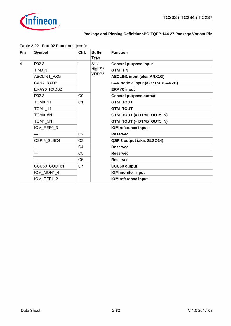
TC233 / TC234 / TC237
Package and Pinning DefinitionsPG-TQFP-144-27 Package Variant Pin
Data Sheet 2-82 V 1.0 2017-03
4 P02.3 I A1 / HighZ / VDDP3
General-purpose inputTIM0_3 GTM_TINASCLIN1_RXG ASCLIN1 input (aka: ARX1G)CAN2_RXDB CAN node 2 input (aka: RXDCAN2B)ERAY0_RXDB2 ERAY0 inputP02.3 O0 General-purpose outputTOM0_11 O1 GTM_TOUTTOM1_11 GTM_TOUTTOM0_5N GTM_TOUT (= DTM1_OUT5_N)TOM1_5N GTM_TOUT (= DTM5_OUT5_N)IOM_REF0_3 IOM reference input— O2 ReservedQSPI3_SLSO4 O3 QSPI3 output (aka: SLSO34)— O4 Reserved— O5 Reserved— O6 ReservedCCU60_COUT61 O7 CCU60 outputIOM_MON1_4 IOM monitor inputIOM_REF1_2 IOM reference input
Table 2-22 Port 02 Functions (cont’d)
Pin Symbol Ctrl. Buffer Type
Function

TC233 / TC234 / TC237
Package and Pinning DefinitionsPG-TQFP-144-27 Package Variant Pin
Data Sheet 2-83 V 1.0 2017-03
5 P02.4 I A1+ / HighZ / VDDP3
General-purpose inputTIM0_4 GTM_TINQSPI3_SLSIA QSPI3 input (aka: SLSI3A)CAN0_RXDD CAN node 0 input (aka: RXDCAN0D)CCU60_CC62INA CCU60 inputCCU61_CC62INB CCU61 inputP02.4 O0 General-purpose outputTOM0_12 O1 GTM_TOUTTOM1_12 GTM_TOUTTOM0_6 GTM_TOUT (= DTM1_OUT6)TOM1_6 GTM_TOUT (= DTM5_OUT6)IOM_REF0_4 IOM reference input— O2 ReservedQSPI3_SLSO0 O3 QSPI3 output (aka: SLSO30)— O4 ReservedCAN10_TXD O5 CAN1 node 0 output (aka: TXDCAN10)ERAY0_TXENA O6 ERAY0 outputCCU60_CC62 O7 CCU60 outputIOM_MON1_0 IOM monitor inputIOM_REF1_4 IOM reference input
Table 2-22 Port 02 Functions (cont’d)
Pin Symbol Ctrl. Buffer Type
Function

TC233 / TC234 / TC237
Package and Pinning DefinitionsPG-TQFP-144-27 Package Variant Pin
Data Sheet 2-84 V 1.0 2017-03
6 P02.5 I A1+ / HighZ / VDDP3
General-purpose inputTIM0_5 GTM_TINQSPI3_MRSTA QSPI3 input (aka: MRST3A)SENT_SENT3C SENT inputP02.5 O0 General-purpose outputTOM0_13 O1 GTM_TOUTTOM1_13 GTM_TOUTTOM0_6N GTM_TOUT (= DTM1_OUT6_N)TOM1_6N GTM_TOUT (= DTM5_OUT6_N)IOM_REF0_5 IOM reference inputCAN0_TXD O2 CAN node 0 output (aka: TXDCAN0)IOM_MON2_5 IOM monitor inputIOM_REF2_5 IOM reference inputQSPI3_MRST O3 QSPI3 output (aka: MRST3)IOM_MON2_3 IOM monitor inputIOM_REF2_3 IOM reference input— O4 ReservedCAN11_TXD O5 CAN1 node 1 output (aka: TXDCAN11)ERAY0_TXENB O6 ERAY0 outputCCU60_COUT62 O7 CCU60 outputIOM_MON1_5 IOM monitor inputIOM_REF1_1 IOM reference input
Table 2-22 Port 02 Functions (cont’d)
Pin Symbol Ctrl. Buffer Type
Function

TC233 / TC234 / TC237
Package and Pinning DefinitionsPG-TQFP-144-27 Package Variant Pin
Data Sheet 2-85 V 1.0 2017-03
7 P02.6 I A1 / HighZ / VDDP3
General-purpose inputTIM0_6 GTM_TINQSPI3_MTSRA QSPI3 input (aka: MTSR3A)SENT_SENT2C SENT inputCCU60_CC60INC CCU60 inputCCU60_CCPOS0A CCU60 inputCCU61_T12HRB CCU61 inputGPT120_T3INA GPT120 inputCAN10_RXDF CAN1 node 0 input (aka: RXDCAN10F)P02.6 O0 General-purpose outputTOM0_14 O1 GTM_TOUTTOM1_14 GTM_TOUTTOM0_7 GTM_TOUT (= DTM1_OUT7)TOM1_7 GTM_TOUT (= DTM5_OUT7)IOM_REF0_6 IOM reference input— O2 ReservedQSPI3_MTSR O3 QSPI3 output (aka: MTSR3)— O4 ReservedVADC_EMUX00 O5 VADC output— O6 ReservedCCU60_CC60 O7 CCU60 outputIOM_MON1_2 IOM monitor inputIOM_REF1_6 IOM reference input
Table 2-22 Port 02 Functions (cont’d)
Pin Symbol Ctrl. Buffer Type
Function

TC233 / TC234 / TC237
Package and Pinning DefinitionsPG-TQFP-144-27 Package Variant Pin
Data Sheet 2-86 V 1.0 2017-03
8 P02.7 I A1 / HighZ / VDDP3
General-purpose inputTIM0_7 GTM_TINQSPI3_SCLKA QSPI3 input (aka: SCLK3A)SENT_SENT1C SENT inputCCU60_CC61INC CCU60 inputCCU60_CCPOS1A CCU60 inputCCU61_T13HRB CCU61 inputGPT120_T3EUDA GPT120 inputCAN11_RXDF CAN1 node 1 input (aka: RXDCAN11F)PMU_FDEST PMU inputP02.7 O0 General-purpose outputTOM0_15 O1 GTM_TOUTTOM1_15 GTM_TOUTTOM0_7N GTM_TOUT (= DTM1_OUT7_N)TOM1_7N GTM_TOUT (= DTM5_OUT7_N)IOM_REF0_7 IOM reference input— O2 ReservedQSPI3_SCLK O3 QSPI3 output (aka: SCLK3)— O4 ReservedVADC_EMUX01 O5 VADC outputSENT_SPC1 O6 SENT outputCCU60_CC61 O7 CCU60 outputIOM_MON1_1 IOM monitor inputIOM_REF1_5 IOM reference input
Table 2-22 Port 02 Functions (cont’d)
Pin Symbol Ctrl. Buffer Type
Function

TC233 / TC234 / TC237
Package and Pinning DefinitionsPG-TQFP-144-27 Package Variant Pin
Data Sheet 2-87 V 1.0 2017-03
9 P02.8 I A1 / HighZ / VDDP3
General-purpose inputTIM0_0 GTM_TINSENT_SENT0C SENT inputCCU60_CC62INC CCU60 inputCCU60_CCPOS2A CCU60 inputCCU61_T12HRC CCU61 inputCCU61_T13HRC CCU61 inputGPT120_T4INA GPT120 inputP02.8 O0 General-purpose outputTOM0_8 O1 GTM_TOUTTOM1_0 GTM_TOUTTOM0_4N GTM_TOUT (= DTM1_OUT4_N)TOM1_4N GTM_TOUT (= DTM5_OUT4_N)IOM_REF0_8 IOM reference inputQSPI3_SLSO5 O2 QSPI3 output (aka: SLSO35)— O3 Reserved— O4 ReservedVADC_EMUX02 O5 VADC outputETH0_MDC O6 Ethernet outputCCU60_CC62 O7 CCU60 outputIOM_MON1_0 IOM monitor inputIOM_REF1_4 IOM reference input
Table 2-22 Port 02 Functions (cont’d)
Pin Symbol Ctrl. Buffer Type
Function

TC233 / TC234 / TC237
Package and Pinning DefinitionsPG-TQFP-144-27 Package Variant Pin
Data Sheet 2-88 V 1.0 2017-03
Table 2-23 Port 10 FunctionsPin Symbol Ctrl. Buffer
TypeFunction
140 P10.1 I A1+ / HighZ / VDDP3
General-purpose inputTIM0_1 GTM_TINQSPI1_MRSTA QSPI1 input (aka: MRST1A)GPT120_T5EUDB GPT120 inputETH0_CRSC Ethernet inputP10.1 O0 General-purpose outputTOM0_1 O1 GTM_TOUTTOM1_9 GTM_TOUTQSPI1_MTSR O2 QSPI1 output (aka: MTSR1)QSPI1_MRST O3 QSPI1 output (aka: MRST1)IOM_MON2_1 IOM monitor inputIOM_REF2_1 IOM reference input— O4 Reserved— O5 Reserved— O6 Reserved— O7 Reserved
141 P10.2 I A1+ / HighZ / VDDP3
General-purpose inputTIM0_2 GTM_TINQSPI1_SCLKA QSPI1 input (aka: SCLK1A)CAN2_RXDE CAN node 2 input (aka: RXDCAN2E)SCU_REQ2 SCU inputGPT120_T6INB GPT120 inputETH0_COLB Ethernet inputP10.2 O0 General-purpose outputTOM0_2 O1 GTM_TOUTTOM1_10 GTM_TOUTIOM_MON2_9 IOM monitor input— O2 ReservedQSPI1_SCLK O3 QSPI1 output (aka: SCLK1)— O4 Reserved— O5 Reserved— O6 Reserved— O7 Reserved

TC233 / TC234 / TC237
Package and Pinning DefinitionsPG-TQFP-144-27 Package Variant Pin
Data Sheet 2-89 V 1.0 2017-03
142 P10.3 I A1+ / HighZ / VDDP3
General-purpose inputTIM0_3 GTM_TINQSPI1_MTSRA QSPI1 input (aka: MTSR1A)SCU_REQ3 SCU inputGPT120_T5INB GPT120 inputETH0_RXERC Ethernet inputP10.3 O0 General-purpose outputTOM0_3 O1 GTM_TOUTTOM1_11 GTM_TOUTIOM_MON2_10 IOM monitor input— O2 ReservedQSPI1_MTSR O3 QSPI1 output (aka: MTSR1)— O4 Reserved— O5 ReservedCAN2_TXD O6 CAN node 2 output (aka: TXDCAN2)IOM_MON2_7 IOM monitor inputIOM_REF2_7 IOM reference input— O7 Reserved
143 P10.5 I A1 / HighZ / VDDP3
General-purpose inputTIM0_2 GTM_TINSCU_HWCFG4 SCU inputCAN10_RXDA CAN1 node 0 input (aka: RXDCAN10A)ETH0_RXD3B Ethernet inputP10.5 O0 General-purpose outputTOM0_2 O1 GTM_TOUTTOM1_10 GTM_TOUTIOM_REF2_9 IOM reference input— O2 ReservedQSPI3_SLSO8 O3 QSPI3 output (aka: SLSO38)QSPI1_SLSO9 O4 QSPI1 output (aka: SLSO19)GPT120_T6OUT O5 GPT120 output— O6 Reserved— O7 Reserved
Table 2-23 Port 10 Functions (cont’d)
Pin Symbol Ctrl. Buffer Type
Function

TC233 / TC234 / TC237
Package and Pinning DefinitionsPG-TQFP-144-27 Package Variant Pin
Data Sheet 2-90 V 1.0 2017-03
144 P10.6 I A1 / HighZ / VDDP3
General-purpose inputTIM0_3 GTM_TINQSPI3_MTSRB QSPI3 input (aka: MTSR3B)SCU_HWCFG5 SCU inputP10.6 O0 General-purpose outputTOM0_3 O1 GTM_TOUTTOM1_11 GTM_TOUTIOM_REF2_10 IOM reference input— O2 ReservedQSPI3_MTSR O3 QSPI3 output (aka: MTSR3)GPT120_T3OUT O4 GPT120 outputCAN10_TXD O5 CAN1 node 0 output (aka: TXDCAN10)QSPI1_MRST O6 QSPI1 output (aka: MRST1)IOM_MON2_1 IOM monitor inputIOM_REF2_1 IOM reference input— O7 Reserved
Table 2-24 Port 11 FunctionsPin Symbol Ctrl. Buffer
TypeFunction
132 P11.2 I A1+ / HighZ / VDDP3
General-purpose inputP11.2 O0 General-purpose outputTOM0_8 O1 GTM_TOUTTOM1_1 GTM_TOUTTOM0_4N GTM_TOUT (= DTM1_OUT4_N)TOM1_4N GTM_TOUT (= DTM5_OUT4_N)— O2 ReservedQSPI0_SLSO5 O3 QSPI0 output (aka: SLSO05)QSPI1_SLSO5 O4 QSPI1 output (aka: SLSO15)CCU61_COUT63 O5 CCU61 outputIOM_MON1_7 IOM monitor inputIOM_REF1_7 IOM reference inputETH0_TXD1 O6 Ethernet outputCCU60_COUT63 O7 CCU60 outputIOM_MON1_6 IOM monitor inputIOM_REF1_0 IOM reference input
Table 2-23 Port 10 Functions (cont’d)
Pin Symbol Ctrl. Buffer Type
Function

TC233 / TC234 / TC237
Package and Pinning DefinitionsPG-TQFP-144-27 Package Variant Pin
Data Sheet 2-91 V 1.0 2017-03
133 P11.3 I A1+ / HighZ / VDDP3
General-purpose inputQSPI1_MRSTB QSPI1 input (aka: MRST1B)P11.3 O0 General-purpose outputTOM0_10 O1 GTM_TOUTTOM1_2 GTM_TOUTTOM0_5 GTM_TOUT (= DTM1_OUT5)TOM1_5 GTM_TOUT (= DTM5_OUT5)— O2 ReservedQSPI1_MRST O3 QSPI1 output (aka: MRST1)IOM_MON2_1 IOM monitor inputIOM_REF2_1 IOM reference inputERAY0_TXDA O4 ERAY0 outputCCU61_COUT62 O5 CCU61 outputIOM_MON1_13 IOM monitor inputIOM_REF1_8 IOM reference inputETH0_TXD0 O6 Ethernet outputCCU60_COUT62 O7 CCU60 outputIOM_MON1_5 IOM monitor inputIOM_REF1_1 IOM reference input
134 P11.6 I A1+ / HighZ / VDDP3
General-purpose inputQSPI1_SCLKB QSPI1 input (aka: SCLK1B)P11.6 O0 General-purpose outputTOM0_11 O1 GTM_TOUTTOM1_3 GTM_TOUTTOM0_5N GTM_TOUT (= DTM1_OUT5_N)TOM1_5N GTM_TOUT (= DTM5_OUT5_N)ERAY0_TXENB O2 ERAY0 outputQSPI1_SCLK O3 QSPI1 output (aka: SCLK1)ERAY0_TXENA O4 ERAY0 outputCCU61_COUT61 O5 CCU61 outputIOM_MON1_12 IOM monitor inputIOM_REF1_9 IOM reference inputETH0_TXEN O6 Ethernet outputCCU60_COUT61 O7 CCU60 outputIOM_MON1_4 IOM monitor inputIOM_REF1_2 IOM reference input
Table 2-24 Port 11 Functions (cont’d)
Pin Symbol Ctrl. Buffer Type
Function
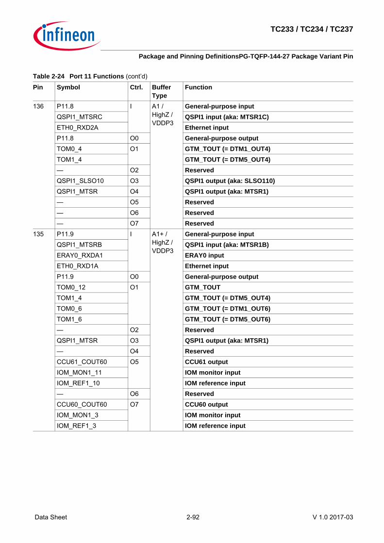
TC233 / TC234 / TC237
Package and Pinning DefinitionsPG-TQFP-144-27 Package Variant Pin
Data Sheet 2-92 V 1.0 2017-03
136 P11.8 I A1 / HighZ / VDDP3
General-purpose inputQSPI1_MTSRC QSPI1 input (aka: MTSR1C)ETH0_RXD2A Ethernet inputP11.8 O0 General-purpose outputTOM0_4 O1 GTM_TOUT (= DTM1_OUT4)TOM1_4 GTM_TOUT (= DTM5_OUT4)— O2 ReservedQSPI1_SLSO10 O3 QSPI1 output (aka: SLSO110)QSPI1_MTSR O4 QSPI1 output (aka: MTSR1)— O5 Reserved— O6 Reserved— O7 Reserved
135 P11.9 I A1+ / HighZ / VDDP3
General-purpose inputQSPI1_MTSRB QSPI1 input (aka: MTSR1B)ERAY0_RXDA1 ERAY0 inputETH0_RXD1A Ethernet inputP11.9 O0 General-purpose outputTOM0_12 O1 GTM_TOUTTOM1_4 GTM_TOUT (= DTM5_OUT4)TOM0_6 GTM_TOUT (= DTM1_OUT6)TOM1_6 GTM_TOUT (= DTM5_OUT6)— O2 ReservedQSPI1_MTSR O3 QSPI1 output (aka: MTSR1)— O4 ReservedCCU61_COUT60 O5 CCU61 outputIOM_MON1_11 IOM monitor inputIOM_REF1_10 IOM reference input— O6 ReservedCCU60_COUT60 O7 CCU60 outputIOM_MON1_3 IOM monitor inputIOM_REF1_3 IOM reference input
Table 2-24 Port 11 Functions (cont’d)
Pin Symbol Ctrl. Buffer Type
Function

TC233 / TC234 / TC237
Package and Pinning DefinitionsPG-TQFP-144-27 Package Variant Pin
Data Sheet 2-93 V 1.0 2017-03
137 P11.10 I A1+ / HighZ / VDDP3
General-purpose inputASCLIN1_RXE ASCLIN1 input (aka: ARX1E)ERAY0_RXDB1 ERAY0 inputSCU_REQ12 SCU inputCAN12_RXDD CAN1 node 2 input (aka: RXDCAN12D)ETH0_RXD0A Ethernet inputP11.10 O0 General-purpose outputTOM0_13 O1 GTM_TOUTTOM1_5 GTM_TOUT (= DTM5_OUT5)TOM0_6N GTM_TOUT (= DTM1_OUT6_N)TOM1_6N GTM_TOUT (= DTM5_OUT6_N)— O2 ReservedQSPI0_SLSO3 O3 QSPI0 output (aka: SLSO03)QSPI1_SLSO3 O4 QSPI1 output (aka: SLSO13)CCU61_CC62 O5 CCU61 outputIOM_MON1_10 IOM monitor inputIOM_REF1_11 IOM reference input— O6 ReservedCCU60_CC62 O7 CCU60 outputIOM_MON1_0 IOM monitor inputIOM_REF1_4 IOM reference input
Table 2-24 Port 11 Functions (cont’d)
Pin Symbol Ctrl. Buffer Type
Function

TC233 / TC234 / TC237
Package and Pinning DefinitionsPG-TQFP-144-27 Package Variant Pin
Data Sheet 2-94 V 1.0 2017-03
138 P11.11 I A1+ / HighZ / VDDP3
General-purpose inputETH0_RXDVA Ethernet inputETH0_CRSDVA Ethernet inputETH0_CRSB Ethernet inputP11.11 O0 General-purpose outputTOM0_14 O1 GTM_TOUTTOM1_6 GTM_TOUT (= DTM5_OUT6)TOM0_7N GTM_TOUT (= DTM1_OUT7_N)TOM1_7N GTM_TOUT (= DTM5_OUT7_N)— O2 ReservedQSPI0_SLSO4 O3 QSPI0 output (aka: SLSO04)QSPI1_SLSO4 O4 QSPI1 output (aka: SLSO14)CCU61_CC61 O5 CCU61 outputIOM_MON1_9 IOM monitor inputIOM_REF1_12 IOM reference inputERAY0_TXENB O6 ERAY0 outputCCU60_CC61 O7 CCU60 outputIOM_MON1_1 IOM monitor inputIOM_REF1_5 IOM reference input
Table 2-24 Port 11 Functions (cont’d)
Pin Symbol Ctrl. Buffer Type
Function

TC233 / TC234 / TC237
Package and Pinning DefinitionsPG-TQFP-144-27 Package Variant Pin
Data Sheet 2-95 V 1.0 2017-03
139 P11.12 I A1+ / HighZ / VDDP3
General-purpose inputETH0_REFCLK Ethernet inputETH0_RXCLKA Ethernet inputETH0_TXCLKB Ethernet inputP11.12 O0 General-purpose outputTOM0_15 O1 GTM_TOUTTOM1_7 GTM_TOUT (= DTM5_OUT7)TOM0_7 GTM_TOUT (= DTM1_OUT7)TOM1_7 GTM_TOUT (= DTM5_OUT7)ASCLIN1_TX O2 ASCLIN1 output (aka: ATX1)IOM_MON2_13 IOM monitor inputIOM_REF2_13 IOM reference inputGTM_CLK2 O3 GTM outputERAY0_TXDB O4 ERAY0 outputCCU61_CC60 O5 CCU61 outputIOM_MON1_8 IOM monitor inputIOM_REF1_13 IOM reference inputSCU_EXTCLK1 O6 SCU outputCCU60_CC60 O7 CCU60 outputIOM_MON1_2 IOM monitor inputIOM_REF1_6 IOM reference input
Table 2-24 Port 11 Functions (cont’d)
Pin Symbol Ctrl. Buffer Type
Function

TC233 / TC234 / TC237
Package and Pinning DefinitionsPG-TQFP-144-27 Package Variant Pin
Data Sheet 2-96 V 1.0 2017-03
Table 2-25 Port 13 FunctionsPin Symbol Ctrl. Buffer
TypeFunction
128 P13.0 I A1 / HighZ / VDDP3
General-purpose inputCCU60_CTRAPA CCU60 inputGPT120_T6EUDB GPT120 inputP13.0 O0 General-purpose outputTOM0_5 O1 GTM_TOUT (= DTM1_OUT5)TOM1_5 GTM_TOUT (= DTM5_OUT5)TOM0_6N GTM_TOUT (= DTM1_OUT6_N)TOM1_6N GTM_TOUT (= DTM5_OUT6_N)— O2 ReservedQSPI2_SCLK O3 QSPI2 output (aka: SCLK2)— O4 Reserved— O5 ReservedETH0_TXER O6 Ethernet outputCAN10_TXD O7 CAN1 node 0 output (aka: TXDCAN10)
129 P13.1 I A1 / HighZ / VDDP3
General-purpose inputCCU60_CCPOS0C CCU60 inputGPT120_T3INB GPT120 inputCAN10_RXDB CAN1 node 0 input (aka: RXDCAN10B)ETH0_TXCLKC Ethernet inputP13.1 O0 General-purpose outputTOM0_6 O1 GTM_TOUT (= DTM1_OUT6)TOM1_6 GTM_TOUT (= DTM5_OUT6)TOM0_7 GTM_TOUT (= DTM1_OUT7)TOM1_7 GTM_TOUT (= DTM5_OUT7)— O2 Reserved— O3 Reserved— O4 Reserved— O5 Reserved— O6 Reserved— O7 Reserved

TC233 / TC234 / TC237
Package and Pinning DefinitionsPG-TQFP-144-27 Package Variant Pin
Data Sheet 2-97 V 1.0 2017-03
130 P13.2 I A1+ / HighZ / VDDP3
General-purpose inputCCU60_CCPOS1C CCU60 inputGPT120_T3EUDB GPT120 inputGPT120_CAPINA GPT120 inputP13.2 O0 General-purpose outputTOM0_7 O1 GTM_TOUT (= DTM1_OUT7)TOM1_7 GTM_TOUT (= DTM5_OUT7)TOM0_7N GTM_TOUT (= DTM1_OUT7_N)TOM1_7N GTM_TOUT (= DTM5_OUT7_N)CAN11_TXD O2 CAN1 node 1 output (aka: TXDCAN11)— O3 Reserved— O4 Reserved— O5 ReservedETH0_TXD3 O6 Ethernet output— O7 Reserved
131 P13.3 I A1+ / HighZ / VDDP3
General-purpose inputCCU60_CCPOS2C CCU60 inputGPT120_T4INB GPT120 inputCAN11_RXDB CAN1 node 1 input (aka: RXDCAN11B)P13.3 O0 General-purpose outputTOM0_8 O1 GTM_TOUTTOM1_0 GTM_TOUTTOM0_4 GTM_TOUT (= DTM1_OUT4)TOM1_4 GTM_TOUT (= DTM5_OUT4)— O2 ReservedQSPI2_MTSR O3 QSPI2 output (aka: MTSR2)— O4 Reserved— O5 ReservedETH0_TXD2 O6 Ethernet output— O7 Reserved
Table 2-25 Port 13 Functions (cont’d)
Pin Symbol Ctrl. Buffer Type
Function

TC233 / TC234 / TC237
Package and Pinning DefinitionsPG-TQFP-144-27 Package Variant Pin
Data Sheet 2-98 V 1.0 2017-03
Table 2-26 Port 14 FunctionsPin Symbol Ctrl. Buffer
TypeFunction
118 P14.0 I A1+ / HighZ / VDDP3
General-purpose inputTIM0_3 GTM_TINP14.0 O0 General-purpose outputTOM0_3 O1 GTM_TOUTTOM1_3 GTM_TOUTTOM0_6 GTM_TOUT (= DTM1_OUT6)TOM1_6 GTM_TOUT (= DTM5_OUT6)ASCLIN0_TX O2 ASCLIN0 output (aka: ATX0)IOM_MON2_12 IOM monitor inputIOM_REF2_12 IOM reference inputERAY0_TXDA O3 ERAY0 outputERAY0_TXDB O4 ERAY0 outputCAN1_TXD O5 CAN node 1 output (aka: TXDCAN1)IOM_MON2_6 IOM monitor inputIOM_REF2_6 IOM reference inputASCLIN0_SCLK O6 ASCLIN0 output (aka: ASCLK0)CCU60_COUT62 O7 CCU60 outputIOM_MON1_5 IOM monitor inputIOM_REF1_1 IOM reference input

TC233 / TC234 / TC237
Package and Pinning DefinitionsPG-TQFP-144-27 Package Variant Pin
Data Sheet 2-99 V 1.0 2017-03
119 P14.1 I A1+ / HighZ / VDDP3
General-purpose inputTIM0_4 GTM_TINASCLIN0_RXA ASCLIN0 input (aka: ARX0A)CAN1_RXDB CAN node 1 input (aka: RXDCAN1B)ERAY0_RXDA3 ERAY0 inputSCU_REQ15 SCU inputERAY0_RXDB3 ERAY0 inputSCU_EVRWUPA AI SCU inputP14.1 O0 General-purpose outputTOM0_4 O1 GTM_TOUT (= DTM1_OUT4)TOM1_4 GTM_TOUT (= DTM5_OUT4)TOM0_7 GTM_TOUT (= DTM1_OUT7)TOM1_7 GTM_TOUT (= DTM5_OUT7)IOM_REF1_14 IOM reference inputASCLIN0_TX O2 ASCLIN0 output (aka: ATX0)IOM_MON2_12 IOM monitor inputIOM_REF2_12 IOM reference input— O3 Reserved— O4 Reserved— O5 Reserved— O6 ReservedCCU60_COUT63 O7 CCU60 outputIOM_MON1_6 IOM monitor inputIOM_REF1_0 IOM reference input
Table 2-26 Port 14 Functions (cont’d)
Pin Symbol Ctrl. Buffer Type
Function

TC233 / TC234 / TC237
Package and Pinning DefinitionsPG-TQFP-144-27 Package Variant Pin
Data Sheet 2-100 V 1.0 2017-03
120 P14.2 I A1 / PU / VDDP3
General-purpose inputTIM0_5 GTM_TINSCU_HWCFG2_EVR13 SCU inputP14.2 O0 General-purpose outputTOM0_5 O1 GTM_TOUT (= DTM1_OUT5)TOM1_5 GTM_TOUT (= DTM5_OUT5)TOM0_6N GTM_TOUT (= DTM1_OUT6_N)TOM1_6N GTM_TOUT (= DTM5_OUT6_N)IOM_REF1_15 IOM reference input— O2 ReservedQSPI2_SLSO1 O3 QSPI2 output (aka: SLSO21)— O4 Reserved— O5 Reserved— O6 Reserved— O7 Reserved
121 P14.3 I A1 / PU / VDDP3
General-purpose inputTIM0_6 GTM_TINSCU_REQ10 SCU inputSCU_HWCFG3_BMI SCU inputP14.3 O0 General-purpose outputTOM0_6 O1 GTM_TOUT (= DTM1_OUT6)TOM1_6 GTM_TOUT (= DTM5_OUT6)IOM_REF2_4 IOM reference input— O2 ReservedQSPI2_SLSO3 O3 QSPI2 output (aka: SLSO23)ASCLIN1_SLSO O4 ASCLIN1 output (aka: ASLSO1)— O5 Reserved— O6 Reserved— O7 Reserved
Table 2-26 Port 14 Functions (cont’d)
Pin Symbol Ctrl. Buffer Type
Function

TC233 / TC234 / TC237
Package and Pinning DefinitionsPG-TQFP-144-27 Package Variant Pin
Data Sheet 2-101 V 1.0 2017-03
122 P14.4 I A1+ / HighZ / VDDP3
General-purpose inputTIM0_7 GTM_TINP14.4 O0 General-purpose outputTOM0_7 O1 GTM_TOUT (= DTM1_OUT7)TOM1_7 GTM_TOUT (= DTM5_OUT7)TOM0_7N GTM_TOUT (= DTM1_OUT7_N)TOM1_7N GTM_TOUT (= DTM5_OUT7_N)IOM_REF2_8 IOM reference input— O2 Reserved— O3 Reserved— O4 Reserved— O5 Reserved— O6 Reserved— O7 Reserved
123 P14.5 I A1+ / HighZ / VDDP3
General-purpose inputTIM0_0 GTM_TINP14.5 O0 General-purpose outputTOM0_0 O1 GTM_TOUTTOM1_0 GTM_TOUTIOM_REF2_11 IOM reference input— O2 Reserved— O3 Reserved— O4 Reserved— O5 ReservedERAY0_TXDB O6 ERAY0 output— O7 Reserved
Table 2-26 Port 14 Functions (cont’d)
Pin Symbol Ctrl. Buffer Type
Function
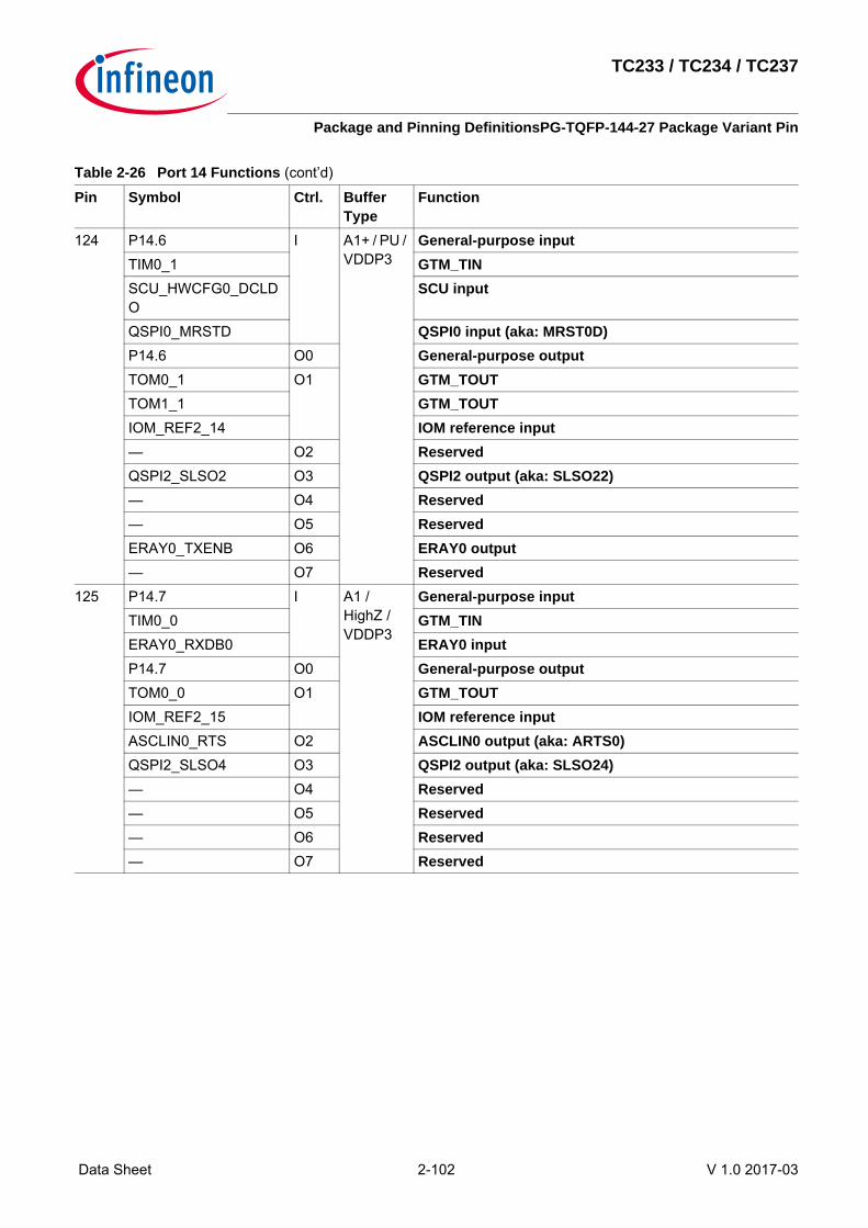
TC233 / TC234 / TC237
Package and Pinning DefinitionsPG-TQFP-144-27 Package Variant Pin
Data Sheet 2-102 V 1.0 2017-03
124 P14.6 I A1+ / PU / VDDP3
General-purpose inputTIM0_1 GTM_TINSCU_HWCFG0_DCLDO
SCU input
QSPI0_MRSTD QSPI0 input (aka: MRST0D)P14.6 O0 General-purpose outputTOM0_1 O1 GTM_TOUTTOM1_1 GTM_TOUTIOM_REF2_14 IOM reference input— O2 ReservedQSPI2_SLSO2 O3 QSPI2 output (aka: SLSO22)— O4 Reserved— O5 ReservedERAY0_TXENB O6 ERAY0 output— O7 Reserved
125 P14.7 I A1 / HighZ / VDDP3
General-purpose inputTIM0_0 GTM_TINERAY0_RXDB0 ERAY0 inputP14.7 O0 General-purpose outputTOM0_0 O1 GTM_TOUTIOM_REF2_15 IOM reference inputASCLIN0_RTS O2 ASCLIN0 output (aka: ARTS0)QSPI2_SLSO4 O3 QSPI2 output (aka: SLSO24)— O4 Reserved— O5 Reserved— O6 Reserved— O7 Reserved
Table 2-26 Port 14 Functions (cont’d)
Pin Symbol Ctrl. Buffer Type
Function

TC233 / TC234 / TC237
Package and Pinning DefinitionsPG-TQFP-144-27 Package Variant Pin
Data Sheet 2-103 V 1.0 2017-03
127 P14.8 I A1 / HighZ / VDDP3
General-purpose inputASCLIN1_RXD ASCLIN1 input (aka: ARX1D)CAN2_RXDD CAN node 2 input (aka: RXDCAN2D)ERAY0_RXDA0 ERAY0 inputP14.8 O0 General-purpose outputTOM0_2 O1 GTM_TOUT— O2 Reserved— O3 Reserved— O4 Reserved— O5 Reserved— O6 Reserved— O7 Reserved
Table 2-27 Port 15 FunctionsPin Symbol Ctrl. Buffer
TypeFunction
109 P15.0 I A1 / HighZ / VDDP3
General-purpose inputP15.0 O0 General-purpose outputTOM1_3 O1 GTM_TOUTTOM0_11 GTM_TOUTTOM0_7N GTM_TOUT (= DTM1_OUT7_N)TOM1_7N GTM_TOUT (= DTM5_OUT7_N)ASCLIN1_TX O2 ASCLIN1 output (aka: ATX1)IOM_MON2_13 IOM monitor inputIOM_REF2_13 IOM reference inputQSPI0_SLSO13 O3 QSPI0 output (aka: SLSO013)— O4 ReservedCAN2_TXD O5 CAN node 2 output (aka: TXDCAN2)IOM_MON2_7 IOM monitor inputIOM_REF2_7 IOM reference inputASCLIN1_SCLK O6 ASCLIN1 output (aka: ASCLK1)— O7 Reserved
Table 2-26 Port 14 Functions (cont’d)
Pin Symbol Ctrl. Buffer Type
Function

TC233 / TC234 / TC237
Package and Pinning DefinitionsPG-TQFP-144-27 Package Variant Pin
Data Sheet 2-104 V 1.0 2017-03
110 P15.1 I A1 / HighZ / VDDP3
General-purpose inputASCLIN1_RXA ASCLIN1 input (aka: ARX1A)QSPI2_SLSIB QSPI2 input (aka: SLSI2B)CAN2_RXDA CAN node 2 input (aka: RXDCAN2A)SCU_REQ16 SCU inputSCU_EVRWUPB AI SCU inputP15.1 O0 General-purpose outputTOM1_4 O1 GTM_TOUT (= DTM5_OUT4)TOM0_12 GTM_TOUTTOM0_4 GTM_TOUT (= DTM1_OUT4)TOM1_4 GTM_TOUT (= DTM5_OUT4)ASCLIN1_TX O2 ASCLIN1 output (aka: ATX1)IOM_MON2_13 IOM monitor inputIOM_REF2_13 IOM reference inputQSPI2_SLSO5 O3 QSPI2 output (aka: SLSO25)— O4 Reserved— O5 Reserved— O6 Reserved— O7 Reserved
111 P15.2 I A1+ / HighZ / VDDP3
General-purpose inputQSPI2_MRSTE QSPI2 input (aka: MRST2E)QSPI2_SLSIA QSPI2 input (aka: SLSI2A)QSPI2_HSICINA QSPI2 input (aka: HSIC2INA)P15.2 O0 General-purpose outputTOM1_5 O1 GTM_TOUT (= DTM5_OUT5)TOM0_13 GTM_TOUTTOM0_4N GTM_TOUT (= DTM1_OUT4_N)TOM1_4N GTM_TOUT (= DTM5_OUT4_N)ASCLIN0_TX O2 ASCLIN0 output (aka: ATX0)IOM_MON2_12 IOM monitor inputIOM_REF2_12 IOM reference inputQSPI2_SLSO0 O3 QSPI2 output (aka: SLSO20)— O4 ReservedCAN1_TXD O5 CAN node 1 output (aka: TXDCAN1)IOM_MON2_6 IOM monitor inputIOM_REF2_6 IOM reference inputASCLIN0_SCLK O6 ASCLIN0 output (aka: ASCLK0)— O7 Reserved
Table 2-27 Port 15 Functions (cont’d)
Pin Symbol Ctrl. Buffer Type
Function

TC233 / TC234 / TC237
Package and Pinning DefinitionsPG-TQFP-144-27 Package Variant Pin
Data Sheet 2-105 V 1.0 2017-03
112 P15.3 I A1+ / HighZ / VDDP3
General-purpose inputASCLIN0_RXB ASCLIN0 input (aka: ARX0B)QSPI2_SCLKA QSPI2 input (aka: SCLK2A)QSPI2_HSICINB QSPI2 input (aka: HSIC2INB)CAN1_RXDA CAN node 1 input (aka: RXDCAN1A)P15.3 O0 General-purpose outputTOM1_6 O1 GTM_TOUT (= DTM5_OUT6)TOM0_14 GTM_TOUTTOM0_5 GTM_TOUT (= DTM1_OUT5)TOM1_5 GTM_TOUT (= DTM5_OUT5)ASCLIN0_TX O2 ASCLIN0 output (aka: ATX0)IOM_MON2_12 IOM monitor inputIOM_REF2_12 IOM reference inputQSPI2_SCLK O3 QSPI2 output (aka: SCLK2)— O4 Reserved— O5 Reserved— O6 Reserved— O7 Reserved
113 P15.4 I A1+ / HighZ / VDDP3
General-purpose inputQSPI2_MRSTA QSPI2 input (aka: MRST2A)SCU_REQ0 SCU inputP15.4 O0 General-purpose outputTOM1_7 O1 GTM_TOUT (= DTM5_OUT7)TOM0_15 GTM_TOUTASCLIN1_TX O2 ASCLIN1 output (aka: ATX1)IOM_MON2_13 IOM monitor inputIOM_REF2_13 IOM reference inputQSPI2_MRST O3 QSPI2 output (aka: MRST2)IOM_MON2_2 IOM monitor inputIOM_REF2_2 IOM reference input— O4 Reserved— O5 Reserved— O6 ReservedCCU60_CC62 O7 CCU60 outputIOM_MON1_0 IOM monitor inputIOM_REF1_4 IOM reference input
Table 2-27 Port 15 Functions (cont’d)
Pin Symbol Ctrl. Buffer Type
Function

TC233 / TC234 / TC237
Package and Pinning DefinitionsPG-TQFP-144-27 Package Variant Pin
Data Sheet 2-106 V 1.0 2017-03
114 P15.5 I A1 / HighZ / VDDP3
General-purpose inputASCLIN1_RXB ASCLIN1 input (aka: ARX1B)QSPI2_MTSRA QSPI2 input (aka: MTSR2A)SCU_REQ13 SCU inputP15.5 O0 General-purpose outputTOM0_0 O1 GTM_TOUTTOM1_0 GTM_TOUTTOM0_5N GTM_TOUT (= DTM1_OUT5_N)TOM1_5N GTM_TOUT (= DTM5_OUT5_N)ASCLIN1_TX O2 ASCLIN1 output (aka: ATX1)IOM_MON2_13 IOM monitor inputIOM_REF2_13 IOM reference inputQSPI2_MTSR O3 QSPI2 output (aka: MTSR2)— O4 Reserved— O5 Reserved— O6 ReservedCCU60_CC61 O7 CCU60 outputIOM_MON1_1 IOM monitor inputIOM_REF1_5 IOM reference input
115 P15.6 I A1 / HighZ / VDDP3
General-purpose inputTIM0_0 GTM_TINQSPI2_MTSRB QSPI2 input (aka: MTSR2B)P15.6 O0 General-purpose outputTOM0_0 O1 GTM_TOUTTOM1_0 GTM_TOUT— O2 ReservedQSPI2_MTSR O3 QSPI2 output (aka: MTSR2)— O4 ReservedQSPI2_SCLK O5 QSPI2 output (aka: SCLK2)— O6 ReservedCCU60_CC60 O7 CCU60 outputIOM_MON1_2 IOM monitor inputIOM_REF1_6 IOM reference input
Table 2-27 Port 15 Functions (cont’d)
Pin Symbol Ctrl. Buffer Type
Function

TC233 / TC234 / TC237
Package and Pinning DefinitionsPG-TQFP-144-27 Package Variant Pin
Data Sheet 2-107 V 1.0 2017-03
116 P15.7 I A1 / HighZ / VDDP3
General-purpose inputTIM0_1 GTM_TINQSPI2_MRSTB QSPI2 input (aka: MRST2B)P15.7 O0 General-purpose outputTOM0_1 O1 GTM_TOUTTOM1_1 GTM_TOUT— O2 ReservedQSPI2_MRST O3 QSPI2 output (aka: MRST2)IOM_MON2_2 IOM monitor inputIOM_REF2_2 IOM reference input— O4 Reserved— O5 Reserved— O6 ReservedCCU60_COUT60 O7 CCU60 outputIOM_MON1_3 IOM monitor inputIOM_REF1_3 IOM reference input
117 P15.8 I A1 / HighZ / VDDP3
General-purpose inputTIM0_2 GTM_TINQSPI2_SCLKB QSPI2 input (aka: SCLK2B)SCU_REQ1 SCU inputP15.8 O0 General-purpose outputTOM0_2 O1 GTM_TOUTTOM1_2 GTM_TOUT— O2 ReservedQSPI2_SCLK O3 QSPI2 output (aka: SCLK2)— O4 Reserved— O5 Reserved— O6 ReservedCCU60_COUT61 O7 CCU60 outputIOM_MON1_4 IOM monitor inputIOM_REF1_2 IOM reference input
Table 2-27 Port 15 Functions (cont’d)
Pin Symbol Ctrl. Buffer Type
Function

TC233 / TC234 / TC237
Package and Pinning DefinitionsPG-TQFP-144-27 Package Variant Pin
Data Sheet 2-108 V 1.0 2017-03
Table 2-28 Port 20 FunctionsPin Symbol Ctrl. Buffer
TypeFunction
93 P20.0 I A1 / HighZ / VDDP3
General-purpose inputTIM0_6 GTM_TINSCU_REQ9 SCU inputOCDS_TGI0 OCDS inputGPT120_T6EUDA GPT120 inputCAN11_RXDC CAN1 node 1 input (aka: RXDCAN11C)CAN12_RXDC CAN1 node 2 input (aka: RXDCAN12C)P20.0 O0 General-purpose outputTOM0_6 O1 GTM_TOUT (= DTM1_OUT6)TOM1_6 GTM_TOUT (= DTM5_OUT6)— O2 Reserved— O3 Reserved— O4 Reserved— O5 Reserved— O6 Reserved— O7 ReservedOCDS_TGO0 O OCDS
94 P20.2 I Input Only / PU / VDDP3
General-purpose inputTESTMODE Factory Test Mode Enable
95 P20.3 I A1 / HighZ / VDDP3
General-purpose inputTIM0_4 GTM_TINGPT120_T6INA GPT120 inputP20.3 O0 General-purpose outputTOM1_12 O1 GTM_TOUTTOM0_4 GTM_TOUT (= DTM1_OUT4)IOM_MON1_14 IOM monitor input— O2 ReservedQSPI0_SLSO9 O3 QSPI0 output (aka: SLSO09)QSPI2_SLSO9 O4 QSPI2 output (aka: SLSO29)CAN12_TXD O5 CAN1 node 2 output (aka: TXDCAN12)— O6 Reserved— O7 Reserved

TC233 / TC234 / TC237
Package and Pinning DefinitionsPG-TQFP-144-27 Package Variant Pin
Data Sheet 2-109 V 1.0 2017-03
100 P20.6 I A1 / HighZ / VDDP3
General-purpose inputTIM0_6 GTM_TINP20.6 O0 General-purpose outputTOM1_10 O1 GTM_TOUTTOM0_10 GTM_TOUTIOM_MON1_15 IOM monitor inputASCLIN1_RTS O2 ASCLIN1 output (aka: ARTS1)QSPI0_SLSO8 O3 QSPI0 output (aka: SLSO08)QSPI2_SLSO8 O4 QSPI2 output (aka: SLSO28)— O5 Reserved— O6 Reserved— O7 Reserved
101 P20.7 I A1 / HighZ / VDDP3
General-purpose inputTIM0_7 GTM_TINASCLIN1_CTSA ASCLIN1 input (aka: ACTS1A)CAN0_RXDB CAN node 0 input (aka: RXDCAN0B)P20.7 O0 General-purpose outputTOM1_11 O1 GTM_TOUTTOM0_11 GTM_TOUTIOM_MON2_4 IOM monitor input— O2 Reserved— O3 Reserved— O4 Reserved— O5 Reserved— O6 ReservedCCU61_COUT63 O7 CCU61 outputIOM_MON1_7 IOM monitor inputIOM_REF1_7 IOM reference input
Table 2-28 Port 20 Functions (cont’d)
Pin Symbol Ctrl. Buffer Type
Function

TC233 / TC234 / TC237
Package and Pinning DefinitionsPG-TQFP-144-27 Package Variant Pin
Data Sheet 2-110 V 1.0 2017-03
102 P20.8 I A1 / HighZ / VDDP3
General-purpose inputTIM0_7 GTM_TINP20.8 O0 General-purpose outputTOM1_7 O1 GTM_TOUT (= DTM5_OUT7)TOM0_7 GTM_TOUT (= DTM1_OUT7)TOM0_4 GTM_TOUT (= DTM1_OUT4)TOM1_4 GTM_TOUT (= DTM5_OUT4)IOM_MON2_8 IOM monitor inputASCLIN1_SLSO O2 ASCLIN1 output (aka: ASLSO1)QSPI0_SLSO0 O3 QSPI0 output (aka: SLSO00)QSPI1_SLSO0 O4 QSPI1 output (aka: SLSO10)CAN0_TXD O5 CAN node 0 output (aka: TXDCAN0)IOM_MON2_5 IOM monitor inputIOM_REF2_5 IOM reference inputSCU_WDT0LCK O6 SCU outputCCU61_CC60 O7 CCU61 outputIOM_MON1_8 IOM monitor inputIOM_REF1_13 IOM reference input
103 P20.9 I A1 / HighZ / VDDP3
General-purpose inputASCLIN1_RXC ASCLIN1 input (aka: ARX1C)QSPI0_SLSIB QSPI0 input (aka: SLSI0B)SCU_REQ11 SCU inputCAN12_RXDE CAN1 node 2 input (aka: RXDCAN12E)P20.9 O0 General-purpose outputTOM1_13 O1 GTM_TOUTTOM0_13 GTM_TOUTTOM0_4N GTM_TOUT (= DTM1_OUT4_N)TOM1_4N GTM_TOUT (= DTM5_OUT4_N)IOM_MON2_11 IOM monitor input— O2 ReservedQSPI0_SLSO1 O3 QSPI0 output (aka: SLSO01)QSPI1_SLSO1 O4 QSPI1 output (aka: SLSO11)— O5 ReservedSCU_WDTSLCK O6 SCU outputCCU61_CC61 O7 CCU61 outputIOM_MON1_9 IOM monitor inputIOM_REF1_12 IOM reference input
Table 2-28 Port 20 Functions (cont’d)
Pin Symbol Ctrl. Buffer Type
Function

TC233 / TC234 / TC237
Package and Pinning DefinitionsPG-TQFP-144-27 Package Variant Pin
Data Sheet 2-111 V 1.0 2017-03
104 P20.10 I A1 / HighZ / VDDP3
General-purpose inputP20.10 O0 General-purpose outputTOM1_14 O1 GTM_TOUTTOM0_14 GTM_TOUTTOM0_5 GTM_TOUT (= DTM1_OUT5)TOM1_5 GTM_TOUT (= DTM5_OUT5)IOM_MON2_14 IOM monitor inputASCLIN1_TX O2 ASCLIN1 output (aka: ATX1)IOM_MON2_13 IOM monitor inputIOM_REF2_13 IOM reference inputQSPI0_SLSO6 O3 QSPI0 output (aka: SLSO06)QSPI2_SLSO7 O4 QSPI2 output (aka: SLSO27)CAN12_TXD O5 CAN1 node 2 output (aka: TXDCAN12)ASCLIN1_SCLK O6 ASCLIN1 output (aka: ASCLK1)CCU61_CC62 O7 CCU61 outputIOM_MON1_10 IOM monitor inputIOM_REF1_11 IOM reference input
105 P20.11 I A1+ / HighZ / VDDP3
General-purpose inputQSPI0_SCLKA QSPI0 input (aka: SCLK0A)P20.11 O0 General-purpose outputTOM1_15 O1 GTM_TOUTTOM0_15 GTM_TOUTTOM0_5N GTM_TOUT (= DTM1_OUT5_N)TOM1_5N GTM_TOUT (= DTM5_OUT5_N)IOM_MON2_15 IOM monitor input— O2 ReservedQSPI0_SCLK O3 QSPI0 output (aka: SCLK0)— O4 ReservedCAN11_TXD O5 CAN1 node 1 output (aka: TXDCAN11)— O6 ReservedCCU61_COUT60 O7 CCU61 outputIOM_MON1_11 IOM monitor inputIOM_REF1_10 IOM reference input
Table 2-28 Port 20 Functions (cont’d)
Pin Symbol Ctrl. Buffer Type
Function
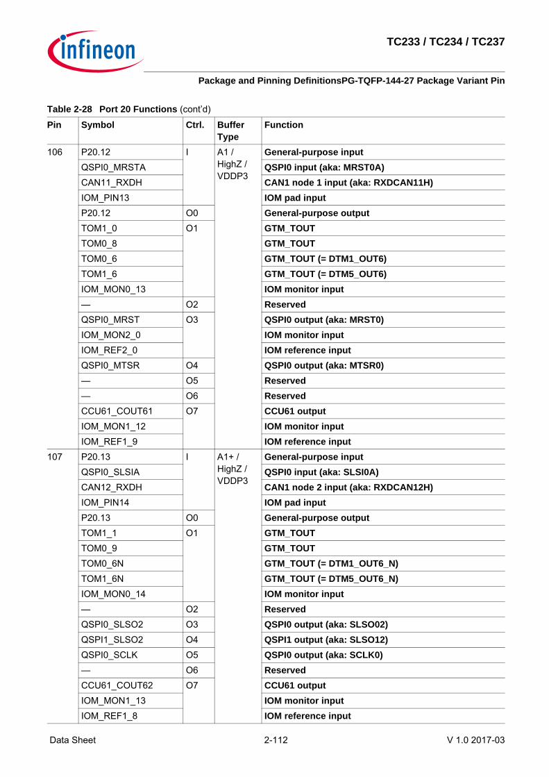
TC233 / TC234 / TC237
Package and Pinning DefinitionsPG-TQFP-144-27 Package Variant Pin
Data Sheet 2-112 V 1.0 2017-03
106 P20.12 I A1 / HighZ / VDDP3
General-purpose inputQSPI0_MRSTA QSPI0 input (aka: MRST0A)CAN11_RXDH CAN1 node 1 input (aka: RXDCAN11H)IOM_PIN13 IOM pad inputP20.12 O0 General-purpose outputTOM1_0 O1 GTM_TOUTTOM0_8 GTM_TOUTTOM0_6 GTM_TOUT (= DTM1_OUT6)TOM1_6 GTM_TOUT (= DTM5_OUT6)IOM_MON0_13 IOM monitor input— O2 ReservedQSPI0_MRST O3 QSPI0 output (aka: MRST0)IOM_MON2_0 IOM monitor inputIOM_REF2_0 IOM reference inputQSPI0_MTSR O4 QSPI0 output (aka: MTSR0)— O5 Reserved— O6 ReservedCCU61_COUT61 O7 CCU61 outputIOM_MON1_12 IOM monitor inputIOM_REF1_9 IOM reference input
107 P20.13 I A1+ / HighZ / VDDP3
General-purpose inputQSPI0_SLSIA QSPI0 input (aka: SLSI0A)CAN12_RXDH CAN1 node 2 input (aka: RXDCAN12H)IOM_PIN14 IOM pad inputP20.13 O0 General-purpose outputTOM1_1 O1 GTM_TOUTTOM0_9 GTM_TOUTTOM0_6N GTM_TOUT (= DTM1_OUT6_N)TOM1_6N GTM_TOUT (= DTM5_OUT6_N)IOM_MON0_14 IOM monitor input— O2 ReservedQSPI0_SLSO2 O3 QSPI0 output (aka: SLSO02)QSPI1_SLSO2 O4 QSPI1 output (aka: SLSO12)QSPI0_SCLK O5 QSPI0 output (aka: SCLK0)— O6 ReservedCCU61_COUT62 O7 CCU61 outputIOM_MON1_13 IOM monitor inputIOM_REF1_8 IOM reference input
Table 2-28 Port 20 Functions (cont’d)
Pin Symbol Ctrl. Buffer Type
Function

TC233 / TC234 / TC237
Package and Pinning DefinitionsPG-TQFP-144-27 Package Variant Pin
Data Sheet 2-113 V 1.0 2017-03
108 P20.14 I A1+ / HighZ / VDDP3
General-purpose inputQSPI0_MTSRA QSPI0 input (aka: MTSR0A)IOM_PIN15 IOM pad inputP20.14 O0 General-purpose outputTOM1_2 O1 GTM_TOUTTOM0_10 GTM_TOUTTOM0_7 GTM_TOUT (= DTM1_OUT7)TOM1_7 GTM_TOUT (= DTM5_OUT7)IOM_MON0_15 IOM monitor input— O2 ReservedQSPI0_MTSR O3 QSPI0 output (aka: MTSR0)— O4 ReservedCAN12_TXD O5 CAN1 node 2 output (aka: TXDCAN12)— O6 Reserved— O7 Reserved
Table 2-29 Port 21 FunctionsPin Symbol Ctrl. Buffer
TypeFunction
84 P21.2 I A1 / HighZ / VDDP3
General-purpose inputTIM0_0 GTM_TINSCU_EMGSTOPB SCU inputP21.2 O0 General-purpose outputTOM0_0 O1 GTM_TOUTTOM1_0 GTM_TOUTTOM0_4 GTM_TOUT (= DTM1_OUT4)TOM1_4 GTM_TOUT (= DTM5_OUT4)— O2 Reserved— O3 Reserved— O4 ReservedETH0_MDC O5 Ethernet output— O6 Reserved— O7 Reserved
Table 2-28 Port 20 Functions (cont’d)
Pin Symbol Ctrl. Buffer Type
Function

TC233 / TC234 / TC237
Package and Pinning DefinitionsPG-TQFP-144-27 Package Variant Pin
Data Sheet 2-114 V 1.0 2017-03
85 P21.3 I A1 / HighZ / VDDP3
General-purpose inputTIM0_1 GTM_TINETH0_MDIOD Ethernet inputP21.3 O0 General-purpose outputTOM0_1 O1 GTM_TOUTTOM1_1 GTM_TOUTTOM0_4N GTM_TOUT (= DTM1_OUT4_N)TOM1_4N GTM_TOUT (= DTM5_OUT4_N)— O2 Reserved— O3 Reserved— O4 Reserved— O5 Reserved— O6 Reserved— O7 ReservedETH0_MDIO O Ethernet output
86 P21.4 I A1 / HighZ / VDDP3
General-purpose inputTIM0_2 GTM_TINP21.4 O0 General-purpose outputTOM0_2 O1 GTM_TOUTTOM1_2 GTM_TOUTTOM0_5 GTM_TOUT (= DTM1_OUT5)TOM1_5 GTM_TOUT (= DTM5_OUT5)— O2 Reserved— O3 Reserved— O4 Reserved— O5 Reserved— O6 Reserved— O7 Reserved
Table 2-29 Port 21 Functions (cont’d)
Pin Symbol Ctrl. Buffer Type
Function

TC233 / TC234 / TC237
Package and Pinning DefinitionsPG-TQFP-144-27 Package Variant Pin
Data Sheet 2-115 V 1.0 2017-03
87 P21.5 I A1 / HighZ / VDDP3
General-purpose inputTIM0_3 GTM_TINP21.5 O0 General-purpose outputTOM0_3 O1 GTM_TOUTTOM1_3 GTM_TOUTTOM0_5N GTM_TOUT (= DTM1_OUT5_N)TOM1_5N GTM_TOUT (= DTM5_OUT5_N)— O2 Reserved— O3 Reserved— O4 Reserved— O5 Reserved— O6 Reserved— O7 Reserved
88 P21.6 I A1 / PU / VDDP3
General-purpose inputTIM0_4 GTM_TINTDI OCDS inputOCDS_TGI2 OCDS inputGPT120_T5EUDA GPT120 inputP21.6 O0 General-purpose outputTOM0_4 O1 GTM_TOUT (= DTM1_OUT4)TOM1_4 GTM_TOUT (= DTM5_OUT4)— O2 Reserved— O3 Reserved— O4 Reserved— O5 Reserved— O6 ReservedGPT120_T3OUT O7 GPT120 outputOCDS_TGO2 O OCDS
Table 2-29 Port 21 Functions (cont’d)
Pin Symbol Ctrl. Buffer Type
Function

TC233 / TC234 / TC237
Package and Pinning DefinitionsPG-TQFP-144-27 Package Variant Pin
Data Sheet 2-116 V 1.0 2017-03
90 P21.7 I A1+ / PU / VDDP3
General-purpose inputTIM0_5 GTM_TINOCDS_DAP2 OCDS inputOCDS_TGI3 OCDS inputGPT120_T5INA GPT120 inputETH0_RXERB Ethernet inputP21.7 O0 General-purpose outputTOM0_5 O1 GTM_TOUT (= DTM1_OUT5)TOM1_5 GTM_TOUT (= DTM5_OUT5)— O2 Reserved— O3 Reserved— O4 Reserved— O5 Reserved— O6 ReservedGPT120_T6OUT O7 GPT120 outputOCDS_TGO3 O OCDSOCDS_DAP2 O OCDS OutputTDO O JTAG Output
Table 2-30 Port 22 FunctionsPin Symbol Ctrl. Buffer
TypeFunction
74 P22.0 I A1 / HighZ / VDDP3
General-purpose inputTIM0_1 GTM_TINQSPI3_MTSRE QSPI3 input (aka: MTSR3E)P22.0 O0 General-purpose outputTOM0_9 O1 GTM_TOUTTOM1_1 GTM_TOUT— O2 ReservedQSPI3_MTSR O3 QSPI3 output (aka: MTSR3)— O4 Reserved— O5 Reserved— O6 Reserved— O7 Reserved
Table 2-29 Port 21 Functions (cont’d)
Pin Symbol Ctrl. Buffer Type
Function

TC233 / TC234 / TC237
Package and Pinning DefinitionsPG-TQFP-144-27 Package Variant Pin
Data Sheet 2-117 V 1.0 2017-03
75 P22.1 I A1 / HighZ / VDDP3
General-purpose inputTIM0_0 GTM_TINQSPI3_MRSTE QSPI3 input (aka: MRST3E)P22.1 O0 General-purpose outputTOM0_8 O1 GTM_TOUTTOM1_0 GTM_TOUTTOM0_6 GTM_TOUT (= DTM1_OUT6)TOM1_6 GTM_TOUT (= DTM5_OUT6)— O2 ReservedQSPI3_MRST O3 QSPI3 output (aka: MRST3)IOM_MON2_3 IOM monitor inputIOM_REF2_3 IOM reference input— O4 Reserved— O5 Reserved— O6 Reserved— O7 Reserved
76 P22.2 I A1 / HighZ / VDDP3
General-purpose inputTIM0_3 GTM_TINQSPI3_SLSID QSPI3 input (aka: SLSI3D)P22.2 O0 General-purpose outputTOM0_11 O1 GTM_TOUTTOM1_3 GTM_TOUTTOM0_6N GTM_TOUT (= DTM1_OUT6_N)TOM1_6N GTM_TOUT (= DTM5_OUT6_N)— O2 ReservedQSPI3_SLSO12 O3 QSPI3 output (aka: SLSO312)— O4 Reserved— O5 Reserved— O6 Reserved— O7 Reserved
Table 2-30 Port 22 Functions (cont’d)
Pin Symbol Ctrl. Buffer Type
Function

TC233 / TC234 / TC237
Package and Pinning DefinitionsPG-TQFP-144-27 Package Variant Pin
Data Sheet 2-118 V 1.0 2017-03
77 P22.3 I A1 / HighZ / VDDP3
General-purpose inputTIM0_4 GTM_TINQSPI3_SCLKE QSPI3 input (aka: SCLK3E)P22.3 O0 General-purpose outputTOM0_12 O1 GTM_TOUTTOM1_4 GTM_TOUT (= DTM5_OUT4)TOM0_7 GTM_TOUT (= DTM1_OUT7)TOM1_7 GTM_TOUT (= DTM5_OUT7)— O2 ReservedQSPI3_SCLK O3 QSPI3 output (aka: SCLK3)— O4 Reserved— O5 Reserved— O6 Reserved— O7 Reserved
78 P22.4 I A1 / HighZ / VDDP3
General-purpose inputP22.4 O0 General-purpose outputTOM0_7N O1 GTM_TOUT (= DTM1_OUT7_N)TOM1_7N GTM_TOUT (= DTM5_OUT7_N)— O2 Reserved— O3 ReservedQSPI0_SLSO12 O4 QSPI0 output (aka: SLSO012)— O5 Reserved— O6 Reserved— O7 Reserved
Table 2-30 Port 22 Functions (cont’d)
Pin Symbol Ctrl. Buffer Type
Function

TC233 / TC234 / TC237
Package and Pinning DefinitionsPG-TQFP-144-27 Package Variant Pin
Data Sheet 2-119 V 1.0 2017-03
Table 2-31 Port 23 FunctionsPin Symbol Ctrl. Buffer
TypeFunction
73 P23.1 I A1+ / HighZ / VDDP3
General-purpose inputTIM0_6 GTM_TINP23.1 O0 General-purpose outputTOM0_6 O1 GTM_TOUT (= DTM1_OUT6)TOM0_15 GTM_TOUTASCLIN1_RTS O2 ASCLIN1 output (aka: ARTS1)QSPI3_SLSO13 O3 QSPI3 output (aka: SLSO313)GTM_CLK0 O4 GTM outputSCU_EXTCLK1 O5 SCU outputSCU_EXTCLK0 O6 SCU output— O7 Reserved
Table 2-32 Port 33 FunctionsPin Symbol Ctrl. Buffer
TypeFunction
56 P33.0 I A1 / HighZ / VDDP3
General-purpose inputTIM0_4 GTM_TINIOM_PIN0 IOM pad inputP33.0 O0 General-purpose outputTOM0_4 O1 GTM_TOUT (= DTM1_OUT4)TOM1_4 GTM_TOUT (= DTM5_OUT4)IOM_MON0_0 IOM monitor input— O2 Reserved— O3 Reserved— O4 Reserved— O5 ReservedVADC_G1BFL0 O6 VADC output— O7 Reserved
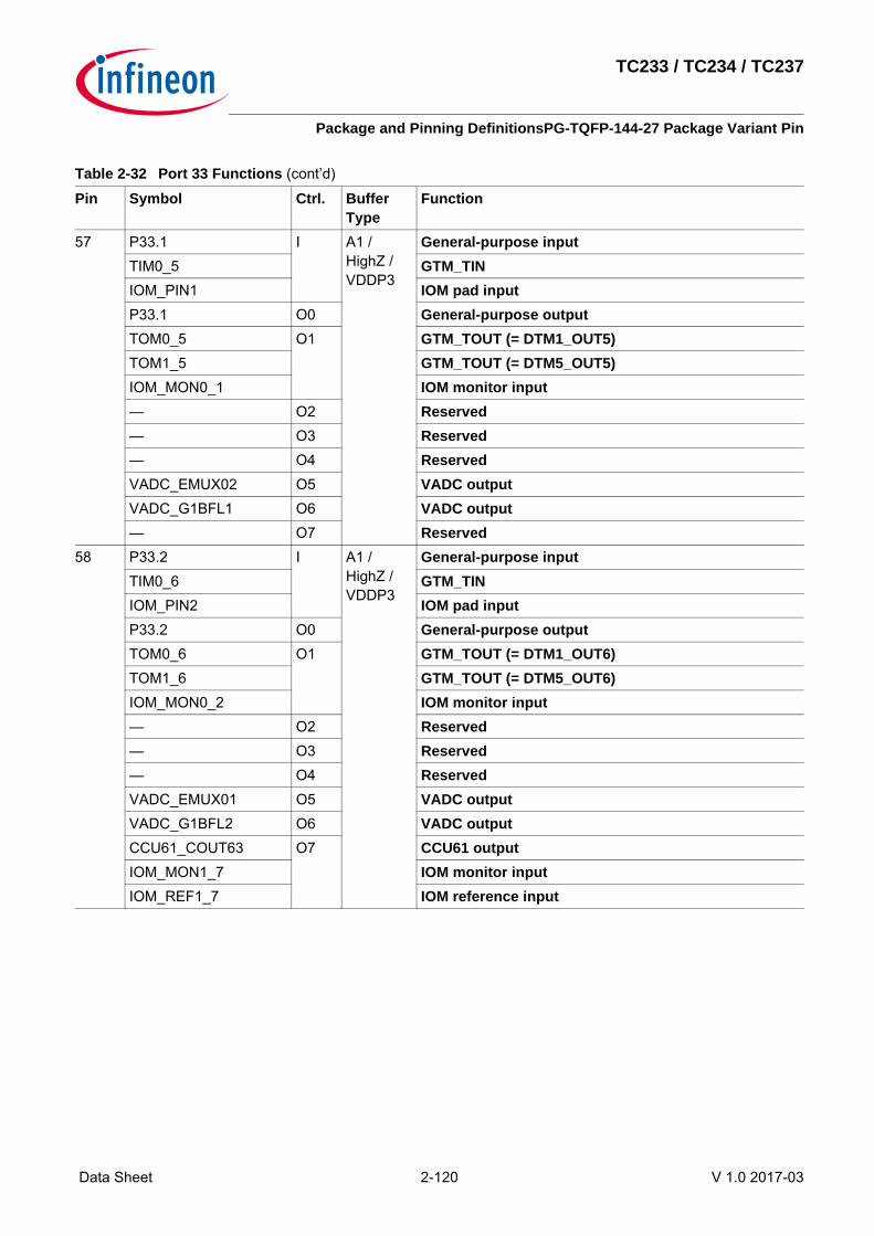
TC233 / TC234 / TC237
Package and Pinning DefinitionsPG-TQFP-144-27 Package Variant Pin
Data Sheet 2-120 V 1.0 2017-03
57 P33.1 I A1 / HighZ / VDDP3
General-purpose inputTIM0_5 GTM_TINIOM_PIN1 IOM pad inputP33.1 O0 General-purpose outputTOM0_5 O1 GTM_TOUT (= DTM1_OUT5)TOM1_5 GTM_TOUT (= DTM5_OUT5)IOM_MON0_1 IOM monitor input— O2 Reserved— O3 Reserved— O4 ReservedVADC_EMUX02 O5 VADC outputVADC_G1BFL1 O6 VADC output— O7 Reserved
58 P33.2 I A1 / HighZ / VDDP3
General-purpose inputTIM0_6 GTM_TINIOM_PIN2 IOM pad inputP33.2 O0 General-purpose outputTOM0_6 O1 GTM_TOUT (= DTM1_OUT6)TOM1_6 GTM_TOUT (= DTM5_OUT6)IOM_MON0_2 IOM monitor input— O2 Reserved— O3 Reserved— O4 ReservedVADC_EMUX01 O5 VADC outputVADC_G1BFL2 O6 VADC outputCCU61_COUT63 O7 CCU61 outputIOM_MON1_7 IOM monitor inputIOM_REF1_7 IOM reference input
Table 2-32 Port 33 Functions (cont’d)
Pin Symbol Ctrl. Buffer Type
Function

TC233 / TC234 / TC237
Package and Pinning DefinitionsPG-TQFP-144-27 Package Variant Pin
Data Sheet 2-121 V 1.0 2017-03
59 P33.3 I A1 / HighZ / VDDP3
General-purpose inputTIM0_7 GTM_TINIOM_PIN3 IOM pad inputP33.3 O0 General-purpose outputTOM0_7 O1 GTM_TOUT (= DTM1_OUT7)TOM1_7 GTM_TOUT (= DTM5_OUT7)IOM_MON0_3 IOM monitor input— O2 Reserved— O3 Reserved— O4 ReservedVADC_EMUX00 O5 VADC outputVADC_G1BFL3 O6 VADC outputCCU61_CC60 O7 CCU61 outputIOM_MON1_8 IOM monitor inputIOM_REF1_13 IOM reference input
60 P33.4 I A1 / HighZ / VDDP3
General-purpose inputTIM0_0 GTM_TINCCU61_CTRAPC CCU61 inputIOM_PIN4 IOM pad inputP33.4 O0 General-purpose outputTOM0_0 O1 GTM_TOUTTOM1_0 GTM_TOUTIOM_MON0_4 IOM monitor input— O2 Reserved— O3 Reserved— O4 ReservedVADC_EMUX12 O5 VADC outputVADC_G0BFL0 O6 VADC output— O7 Reserved
Table 2-32 Port 33 Functions (cont’d)
Pin Symbol Ctrl. Buffer Type
Function
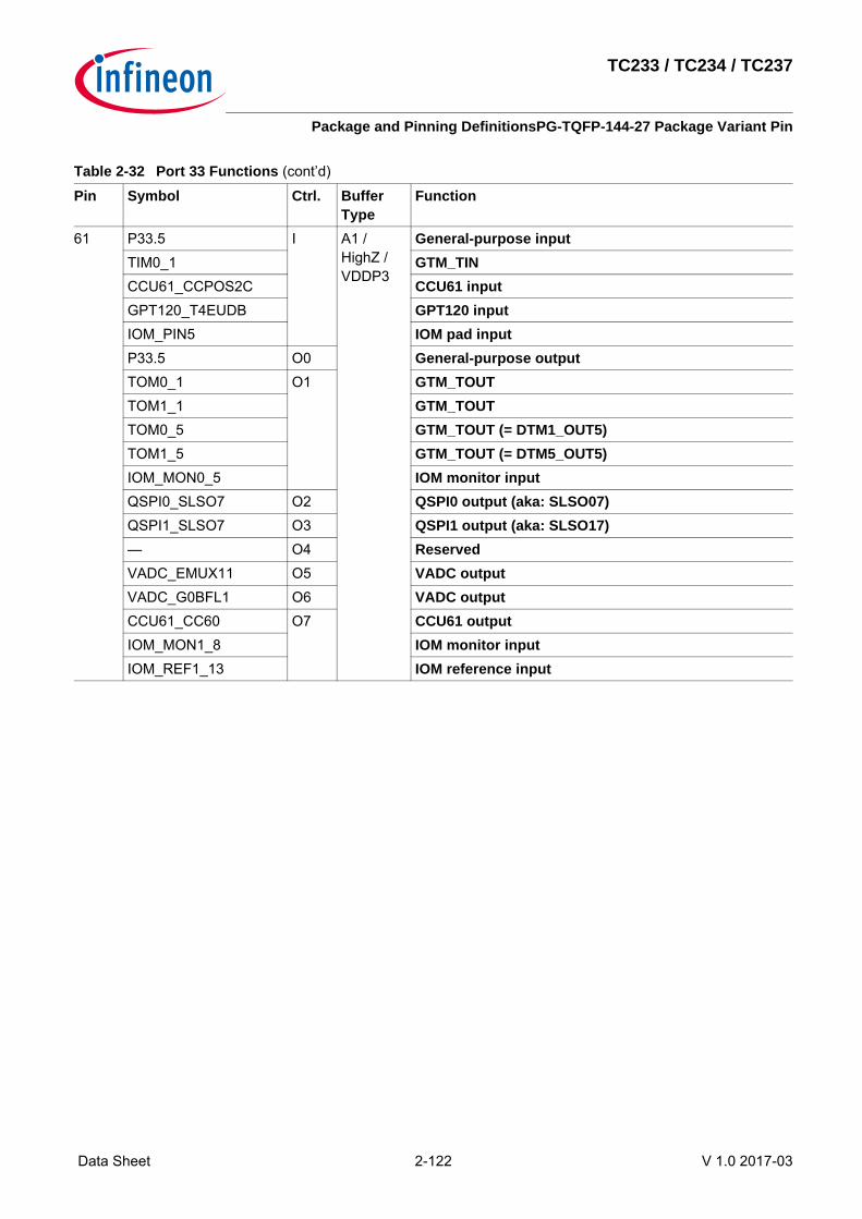
TC233 / TC234 / TC237
Package and Pinning DefinitionsPG-TQFP-144-27 Package Variant Pin
Data Sheet 2-122 V 1.0 2017-03
61 P33.5 I A1 / HighZ / VDDP3
General-purpose inputTIM0_1 GTM_TINCCU61_CCPOS2C CCU61 inputGPT120_T4EUDB GPT120 inputIOM_PIN5 IOM pad inputP33.5 O0 General-purpose outputTOM0_1 O1 GTM_TOUTTOM1_1 GTM_TOUTTOM0_5 GTM_TOUT (= DTM1_OUT5)TOM1_5 GTM_TOUT (= DTM5_OUT5)IOM_MON0_5 IOM monitor inputQSPI0_SLSO7 O2 QSPI0 output (aka: SLSO07)QSPI1_SLSO7 O3 QSPI1 output (aka: SLSO17)— O4 ReservedVADC_EMUX11 O5 VADC outputVADC_G0BFL1 O6 VADC outputCCU61_CC60 O7 CCU61 outputIOM_MON1_8 IOM monitor inputIOM_REF1_13 IOM reference input
Table 2-32 Port 33 Functions (cont’d)
Pin Symbol Ctrl. Buffer Type
Function

TC233 / TC234 / TC237
Package and Pinning DefinitionsPG-TQFP-144-27 Package Variant Pin
Data Sheet 2-123 V 1.0 2017-03
62 P33.6 I A1 / HighZ / VDDP3
General-purpose inputTIM0_2 GTM_TINASCLIN1_RXF ASCLIN1 input (aka: ARX1F)CCU61_CCPOS1C CCU61 inputGPT120_T2EUDB GPT120 inputCAN10_RXDH CAN1 node 0 input (aka: RXDCAN10H)IOM_PIN6 IOM pad inputP33.6 O0 General-purpose outputTOM0_2 O1 GTM_TOUTTOM1_2 GTM_TOUTTOM0_5N GTM_TOUT (= DTM1_OUT5_N)TOM1_5N GTM_TOUT (= DTM5_OUT5_N)IOM_MON0_6 IOM monitor input— O2 Reserved— O3 ReservedASCLIN1_TX O4 ASCLIN1 output (aka: ATX1)IOM_MON2_13 IOM monitor inputIOM_REF2_13 IOM reference inputVADC_EMUX10 O5 VADC outputVADC_G0BFL2 O6 VADC outputCCU61_CC61 O7 CCU61 outputIOM_MON1_9 IOM monitor inputIOM_REF1_12 IOM reference inputHSM_HSM1 O HSM output
Table 2-32 Port 33 Functions (cont’d)
Pin Symbol Ctrl. Buffer Type
Function

TC233 / TC234 / TC237
Package and Pinning DefinitionsPG-TQFP-144-27 Package Variant Pin
Data Sheet 2-124 V 1.0 2017-03
63 P33.7 I A1+ / HighZ / VDDP3
General-purpose inputTIM0_3 GTM_TINCAN0_RXDE CAN node 0 input (aka: RXDCAN0E)SCU_REQ8 SCU inputCCU61_CCPOS0C CCU61 inputGPT120_T2INB GPT120 inputIOM_PIN7 IOM pad inputP33.7 O0 General-purpose outputTOM0_3 O1 GTM_TOUTTOM1_3 GTM_TOUTTOM0_6 GTM_TOUT (= DTM1_OUT6)TOM1_6 GTM_TOUT (= DTM5_OUT6)IOM_MON0_7 IOM monitor input— O2 ReservedQSPI3_SLSO7 O3 QSPI3 output (aka: SLSO37)— O4 ReservedCAN10_TXD O5 CAN1 node 0 output (aka: TXDCAN10)VADC_G0BFL3 O6 VADC outputCCU61_COUT60 O7 CCU61 outputIOM_MON1_11 IOM monitor inputIOM_REF1_10 IOM reference inputHSM_HSM2 O HSM output
Table 2-32 Port 33 Functions (cont’d)
Pin Symbol Ctrl. Buffer Type
Function

TC233 / TC234 / TC237
Package and Pinning DefinitionsPG-TQFP-144-27 Package Variant Pin
Data Sheet 2-125 V 1.0 2017-03
64 P33.8 I A1+ / HighZ / VDDP3
General-purpose inputTIM0_4 GTM_TINSCU_EMGSTOPA SCU inputIOM_PIN8 IOM pad inputP33.8 O0 General-purpose outputTOM0_4 O1 GTM_TOUT (= DTM1_OUT4)TOM1_4 GTM_TOUT (= DTM5_OUT4)TOM0_6N GTM_TOUT (= DTM1_OUT6_N)TOM1_6N GTM_TOUT (= DTM5_OUT6_N)IOM_MON0_8 IOM monitor input— O2 ReservedQSPI3_SLSO2 O3 QSPI3 output (aka: SLSO32)— O4 ReservedCAN0_TXD O5 CAN node 0 output (aka: TXDCAN0)IOM_MON2_5 IOM monitor inputIOM_REF2_5 IOM reference input— O6 ReservedCCU61_COUT62 O7 CCU61 outputIOM_MON1_13 IOM monitor inputIOM_REF1_8 IOM reference inputSMU_FSP O SMU
Table 2-32 Port 33 Functions (cont’d)
Pin Symbol Ctrl. Buffer Type
Function

TC233 / TC234 / TC237
Package and Pinning DefinitionsPG-TQFP-144-27 Package Variant Pin
Data Sheet 2-126 V 1.0 2017-03
65 P33.9 I A1 / HighZ / VDDP3
General-purpose inputTIM0_1 GTM_TINQSPI3_HSICINA QSPI3 inputIOM_PIN9 IOM pad inputP33.9 O0 General-purpose outputTOM0_1 O1 GTM_TOUTTOM1_1 GTM_TOUTTOM0_7 GTM_TOUT (= DTM1_OUT7)TOM1_7 GTM_TOUT (= DTM5_OUT7)IOM_MON0_9 IOM monitor input— O2 ReservedQSPI3_SLSO1 O3 QSPI3 output (aka: SLSO31)— O4 Reserved— O5 Reserved— O6 ReservedCCU61_CC62 O7 CCU61 outputIOM_MON1_10 IOM monitor inputIOM_REF1_11 IOM reference input
66 P33.10 I A1+ / HighZ / VDDP3
General-purpose inputTIM0_0 GTM_TINQSPI3_SLSIC QSPI3 input (aka: SLSI3C)QSPI3_HSICINB QSPI3 inputIOM_PIN10 IOM pad inputP33.10 O0 General-purpose outputTOM0_0 O1 GTM_TOUTTOM1_0 GTM_TOUTTOM0_7N GTM_TOUT (= DTM1_OUT7_N)TOM1_7N GTM_TOUT (= DTM5_OUT7_N)IOM_MON0_10 IOM monitor inputQSPI1_SLSO6 O2 QSPI1 output (aka: SLSO16)QSPI3_SLSO11 O3 QSPI3 output (aka: SLSO311)ASCLIN1_SLSO O4 ASCLIN1 output (aka: ASLSO1)GTM_CLK1 O5 GTM outputSCU_EXTCLK1 O6 SCU outputCCU61_COUT61 O7 CCU61 outputIOM_MON1_12 IOM monitor inputIOM_REF1_9 IOM reference input
Table 2-32 Port 33 Functions (cont’d)
Pin Symbol Ctrl. Buffer Type
Function

TC233 / TC234 / TC237
Package and Pinning DefinitionsPG-TQFP-144-27 Package Variant Pin
Data Sheet 2-127 V 1.0 2017-03
67 P33.11 I A1 / HighZ / VDDP3
General-purpose inputTIM0_2 GTM_TINQSPI3_SCLKD QSPI3 input (aka: SCLK3D)SCU_REQ17 SCU inputIOM_PIN11 IOM pad inputP33.11 O0 General-purpose outputTOM0_2 O1 GTM_TOUTTOM1_2 GTM_TOUTIOM_MON0_11 IOM monitor inputASCLIN1_SCLK O2 ASCLIN1 output (aka: ASCLK1)QSPI3_SCLK O3 QSPI3 output (aka: SCLK3)— O4 Reserved— O5 ReservedSMPS_DCDCSYNC O6 SCU outputCCU61_CC61 O7 CCU61 outputIOM_MON1_9 IOM monitor inputIOM_REF1_12 IOM reference inputSMPS_DCDCSYNC O SCU output
68 P33.12 I A1 / HighZ / VDDP3
General-purpose inputTIM0_0 GTM_TINQSPI3_MTSRD QSPI3 input (aka: MTSR3D)IOM_PIN12 IOM pad inputP33.12 O0 General-purpose outputTOM1_12 O1 GTM_TOUTTOM0_12 GTM_TOUTIOM_MON0_12 IOM monitor inputASCLIN1_TX O2 ASCLIN1 output (aka: ATX1)IOM_MON2_13 IOM monitor inputIOM_REF2_13 IOM reference inputQSPI3_MTSR O3 QSPI3 output (aka: MTSR3)ASCLIN1_SCLK O4 ASCLIN1 output (aka: ASCLK1)— O5 Reserved— O6 ReservedCCU61_COUT60 O7 CCU61 outputIOM_MON1_11 IOM monitor inputIOM_REF1_10 IOM reference input
Table 2-32 Port 33 Functions (cont’d)
Pin Symbol Ctrl. Buffer Type
Function

TC233 / TC234 / TC237
Package and Pinning DefinitionsPG-TQFP-144-27 Package Variant Pin
Data Sheet 2-128 V 1.0 2017-03
Table 2-33 Port 34 FunctionsPin Symbol Ctrl. Buffer
TypeFunction
52 P34.0 I A1 / HighZ / VDDP3
General-purpose inputP34.0 O0 General-purpose outputTOM1_12 O1 GTM_TOUT— O2 Reserved— O3 Reserved— O4 Reserved— O5 Reserved— O6 Reserved— O7 Reserved
53 P34.1 I A1 / HighZ / VDDP3
General-purpose inputP34.1 O0 General-purpose outputTOM1_13 O1 GTM_TOUTASCLIN0_TX O2 ASCLIN0 output (aka: ATX0)IOM_MON2_12 IOM monitor inputIOM_REF2_12 IOM reference input— O3 ReservedCAN0_TXD O4 CAN node 0 output (aka: TXDCAN0)IOM_MON2_5 IOM monitor inputIOM_REF2_5 IOM reference input— O5 Reserved— O6 Reserved— O7 Reserved
54 P34.2 I A1 / HighZ / VDDP3
General-purpose inputASCLIN0_RXD ASCLIN0 input (aka: ARX0D)CAN0_RXDG CAN node 0 input (aka: RXDCAN0G)P34.2 O0 General-purpose outputTOM1_14 O1 GTM_TOUT— O2 Reserved— O3 Reserved— O4 Reserved— O5 Reserved— O6 Reserved— O7 Reserved

TC233 / TC234 / TC237
Package and Pinning DefinitionsPG-TQFP-144-27 Package Variant Pin
Data Sheet 2-129 V 1.0 2017-03
55 P34.3 I A1 / HighZ / VDDP3
General-purpose inputASCLIN1_CTSB ASCLIN1 input (aka: ACTS1B)P34.3 O0 General-purpose outputTOM1_15 O1 GTM_TOUT— O2 Reserved— O3 ReservedQSPI2_SLSO10 O4 QSPI2 output (aka: SLSO210)— O5 Reserved— O6 Reserved— O7 Reserved
Table 2-34 Port 40 FunctionsPin Symbol Ctrl. Buffer
TypeFunction
51 P40.0 I S / VDDM General-purpose inputVADCG0_0 AI VADC input channel 0 of group 0
50 P40.1 I S / VDDM General-purpose inputVADCG0_1 AI VADC input channel 1 of group 0
(with multiplexer diagnostics)VADCG2_0 VADC input channel 0 of group 2
49 P40.2 I S / VDDM General-purpose inputVADCG0_2 AI VADC input channel 2 of group 0
(with multiplexer diagnostics)48 P40.3 I S / VDDM General-purpose input
VADCG0_3 AI VADC input channel 3 of group 047 P40.4 I S / VDDM General-purpose input
VADCG0_4 AI VADC input channel 4 of group 046 P40.5 I S / VDDM General-purpose input
VADCG0_5 AI VADC input channel 5 of group 045 P40.6 I S / VDDM General-purpose input
VADCG0_6 AI VADC input channel 6 of group 040 P40.7 I S / VDDM General-purpose input
VADCG0_7 AI VADC input channel 7 of group 0(with pull down diagnostics)
39 P40.8 I S / VDDM General-purpose inputVADCG0_8 AI VADC input channel 8 of group 0
38 P40.9 I S / VDDM General-purpose inputVADCG0_9 AI VADC input channel 9 of group 0
(with multiplexer diagnostics)
Table 2-33 Port 34 Functions (cont’d)
Pin Symbol Ctrl. Buffer Type
Function

TC233 / TC234 / TC237
Package and Pinning DefinitionsPG-TQFP-144-27 Package Variant Pin
Data Sheet 2-130 V 1.0 2017-03
37 P40.10 I S / VDDM General-purpose inputVADCG0_10 AI VADC input channel 10 of group 0
(with multiplexer diagnostics)36 P40.11 I S / VDDM General-purpose input
SENT_SENT0A SENT inputCCU60_CCPOS0D CCU60 inputVADCG0_11 AI VADC input channel 11 of group 0
Table 2-35 Port 41 FunctionsPin Symbol Ctrl. Buffer
TypeFunction
35 P41.0 I S / VDDM General-purpose inputSENT_SENT1A SENT inputCCU60_CCPOS1B CCU60 inputVADCG1_0 AI VADC input channel 0 of group 1
34 P41.1 I S / VDDM General-purpose inputVADCG1_1 AI VADC input channel 1 of group 1
(with multiplexer diagnostics)VADCG3_0 VADC input channel 0 of group 3
33 P41.2 I S / VDDM General-purpose inputSENT_SENT2A SENT inputCCU61_CCPOS1B CCU61 inputVADCG1_2 AI VADC input channel 2 of group 1
(with multiplexer diagnostics)32 P41.3 I S / VDDM General-purpose input
SENT_SENT3A SENT inputCCU61_CCPOS1D CCU61 inputVADCG1_3 AI VADC input channel 3 of group 1
(with pull down diagnostics)31 P41.4 I S / VDDM General-purpose input
VADCG1_4 AI VADC input channel 4 of group 130 P41.5 I S / VDDM General-purpose input
VADCG1_5 AI VADC input channel 5 of group 129 P41.6 I S / VDDM General-purpose input
VADCG1_6 AI VADC input channel 6 of group 128 P41.7 I S / VDDM General-purpose input
VADCG1_7 AI VADC input channel 7 of group 127 P41.8 I S / VDDM General-purpose input
VADCG1_8 AI VADC input channel 8 of group 1
Table 2-34 Port 40 Functions (cont’d)
Pin Symbol Ctrl. Buffer Type
Function

TC233 / TC234 / TC237
Package and Pinning DefinitionsPG-TQFP-144-27 Package Variant Pin
Data Sheet 2-131 V 1.0 2017-03
26 P41.9 I S / VDDM General-purpose inputVADCG1_9 AI VADC input channel 9 of group 1
(with multiplexer diagnostics)25 P41.10 I S / VDDM General-purpose input
VADCG1_10 AI VADC input channel 10 of group 1(with multiplexer diagnostics)
24 P41.11 I S / VDDM General-purpose inputVADCG1_11 AI VADC input channel 11 of group 1
Table 2-36 System I/OPin Symbol Ctrl. Buffer
TypeFunction
81 XTAL1 I VDDP3 Main Oscillator/PLL/Clock Generator Input82 XTAL2 O VDDP3 Main Oscillator/PLL/Clock Generator Output89 TMS/DAP1 I A1+ / PD /
VDDP3Debug Interface
DAP1 I/O Device Access Port LIne 191 TRST I Input Only
/ PD / VDDP3
JTAG Module Reset/Enable Input
92 TCK/DAP0 I Input Only / PD / VDDP3
OCDS inputDAP0 I Device Access Port LIne 0
96 ESR1 I/O A1+ / PU / VDDP3
SCU inputEVRWUP I EVR Wakeup Pin
97 PORST I Input Only / PD / VDDP3
Power On ResetAdditional strong PD in case of power fail.
98 ESR0 I/O A1+ / OD / VDDP3
SCU input/outputEVRWUP I EVR Wakeup Pin
Table 2-37 SupplyPin Symbol Ctrl. Buffer
TypeFunction
41 VAGND I — Negative Analog Reference Voltage 042 VAREF I — Positive Analog Reference Voltage 0126 VDDP3 I — Digital I/O Power Supply (3.3V)
This pin supplies also the Flash 3.3V.69 VDDP3 I — Digital I/O Power Supply (3.3V)70 VDD I — Digital Core Power Supply (1.3V)
Output of EVR13.
Table 2-35 Port 41 Functions (cont’d)
Pin Symbol Ctrl. Buffer Type
Function

TC233 / TC234 / TC237
Package and Pinning DefinitionsPG-TQFP-100-23 Package Variant Pin
Data Sheet 2-132 V 1.0 2017-03
2.2.2 Pull-Up/Pull-Down Reset Behavior of the Pins
2.3 PG-TQFP-100-23 Package Variant Pin Configuration of TC233xFigure 2-1 is showing the TC233x pinout for the package variant: PG-TQFP-100-23.
79 VDD I — Digital Core Power Supply (1.3V)This pin supplies also the main XTAL Oscillator/PLL (1.3V). A higher decoupling capacitor is therefore recommended to the VSS pin for better noise immunity.
83 VDDP3 I — Digital I/O Power Supply (3.3V)This pin supplies also the main XTAL Oscillator/PLL (3.3V). A higher decoupling capacitor is therefore recommended to the VSS pin for better noise immunity.
44 VDDM I — ADC Power Supply (5.0V)23 VDDP3 I — Digital I/O Power Supply (3.3V)10 VDD/VDDSB I — Digital Core Power Supply (1.3V)22 VDD I — Digital Core Power Supply (1.3V)99 VDD I — Digital Core Power Supply (1.3V)43 VSSM I — Analog Ground for VDDM80 VSS I — Digital Ground
Table 2-38 List of Pull-Up/Pull-Down Reset Behavior of the PinsPins PORST = 0 PORST = 1all GPIOs High-ZTDI, TESTMODE Pull-upPORST1)
1) Pull-down with IPORST relevant is always activated when a primary supply monitor detects a violation.
Pull-down with IPORST relevant Pull-down with IPDLI relevantTRST, TCK, TMS Pull-downESR0 The open-drain driver is used to
drive low.2)
2) Valid additionally after deactivation of PORST until the internal reset phase has finished. See the SCU chapter for details.
Pull-up3)
3) See the SCU_IOCR register description.
ESR1 Pull-up3)
P14.2, P14.3, P14.6 Pull-upP21.7 / TDO Pull-up High-Z/Pull-up4)
4) Depends on JTAG/DAP selection with TRST.
Table 2-37 Supply (cont’d)
Pin Symbol Ctrl. Buffer Type
Function

TC233 / TC234 / TC237
Package and Pinning DefinitionsPG-TQFP-100-23 Package Variant Pin
Data Sheet 2-133 V 1.0 2017-03
Figure 2-3 TC233x Pinout for the package variant PG-TQFP-100-23.
76P1
5.0
77P1
5.1
78P1
5.2
79P1
5.3
80P1
5.5
81P1
4.0/Bootloader
82P1
4.1/Bootloader
83P1
4.3
84P1
4.4
85P1
4.6
87P1
3.0
88P1
3.1
89P1
3.2
90P1
3.3
91P1
1.2
92P1
1.3
93P1
1.6
94P1
1.9
95P1
1.8
96P1
1.10
97P1
1.11
98P1
1.12
99P1
0.5
100
P10.6
1P02.02P02.13P02.24P02.35P02.46P02.57P02.68P02.79P02.810P00.0
41P3
3.5
42P3
3.6
43P3
3.7
44P3
3.8
45P3
3.9
46P3
3.10
51 P23.1
56 P21.257 P21.358 P21.459 P21.6/TDI
61 P21.7/TDO/DAP2
64 P20.2/TESTMODE
69 P20.870 P20.971 P20.1072 P20.1173 P20.1274 P20.1375 P20.14
86V D
DP3
47V D
DP3
48V D
D
52 VDD
55 VDDP3
49VC
AP0
50VC
AP1
33V D
DM
12VDDP3
11VDD
68 VDD
32V S
SM
30V A
GND
31V A
REF
53 XTAL154 XTAL2
60 TMS/DAP1
62 TRST63 TCK/DAP0
65 ESR166 PORST67 ESR0
13AN23/P41.1114AN22/P41.1015AN21/P41.916AN20/P41.817AN19/P41.718AN18/P41.619AN17/P41.520AN16/P41.421AN15/P41.322AN14/P41.223AN13/P41.124AN12/P41.025AN11/P40.11
26AN
10/P40
.10
27AN
9/P4
0.9
28AN
8/P4
0.8
29AN
7/P4
0.7
34AN
6/P4
0.6
35AN
5/P4
0.5
36AN
4/P4
0.4
37AN
3/P4
0.3
38AN
2/P4
0.2
39AN
1/P4
0.1
40AN
0/P4
0.0
TC23x(Top View)

TC233 / TC234 / TC237
Package and Pinning DefinitionsPG-TQFP-100-23 Package Variant Pin
Data Sheet 2-134 V 1.0 2017-03
2.3.1 Port Functions and Pinning Tables
2.3.1.1 How to Read the Following Port Function TablesSome hints for interpreting the following tables.
Column “Ctrl.”:I = Input (for GPIO port Lines with IOCR bit field Selection PCx = 0XXXB)AI = Analog inputO = OutputO0 = Output with IOCR bit field selection PCx = 1X000BO1 = Output with IOCR bit field selection PCx = 1X001B (ALT1)O2 = Output with IOCR bit field selection PCx = 1X010B (ALT2)O3 = Output with IOCR bit field selection PCx = 1X011B (ALT3)O4 = Output with IOCR bit field selection PCx = 1X100B (ALT4)O5 = Output with IOCR bit field selection PCx = 1X101B (ALT5)O6 = Output with IOCR bit field selection PCx = 1X110B (ALT6)O7 = Output with IOCR bit field selection PCx = 1X111B (ALT7)
To each input several functions can be connected. The peripherals’ configuration defines if this input is used.The port module (see corresponding chapter) decides which of the 8 output signals O0 to O7 drives the pad.Some Ox rows list more than one function, e.g. several GTM_TOUT outputs and IOM reference inputs. The GTMmodule (see corresponding chapter) has its own sub-multiplexer structure that defines which of the GTM sub-unitsdrives this signal. Additionally the IOM modules “listens” on these output signals (see IOM chapter).Some pin symbol names were changed in this AURIX device compared to other AURIX devices to improve namingsystematics. The previously used symbol name is documented in the “Function” column with the text “(aka …)”1).
Column “Type”:IN = Input onlyA1 = Pad class A1 (3.3V)A1+ = Pad class A1+ (3.3V)S = ADC with digital input. Pad class D for analog input “AI”, pad class S for digital input “I”.
PU = with pull-up device connected during reset (PORST = 0)PD = with pull-down device connected during reset (PORST = 0)
Table 2-39 Example Port TablePin Symbol Ctrl. Buffer
TypeFunction
10 Pxx.y I A1 / HighZ / VDDP3
General-purpose inputTIMm_n GTM_TINTOMa_b O1 GTM_TOUTTOMc_d GTM_TOUTIOM_REFv_w IOM reference inputASCLINz_RTS O2 ASCLIN0 output (aka ARTSz)
1) “aka” as abbreviation for “also known as”.
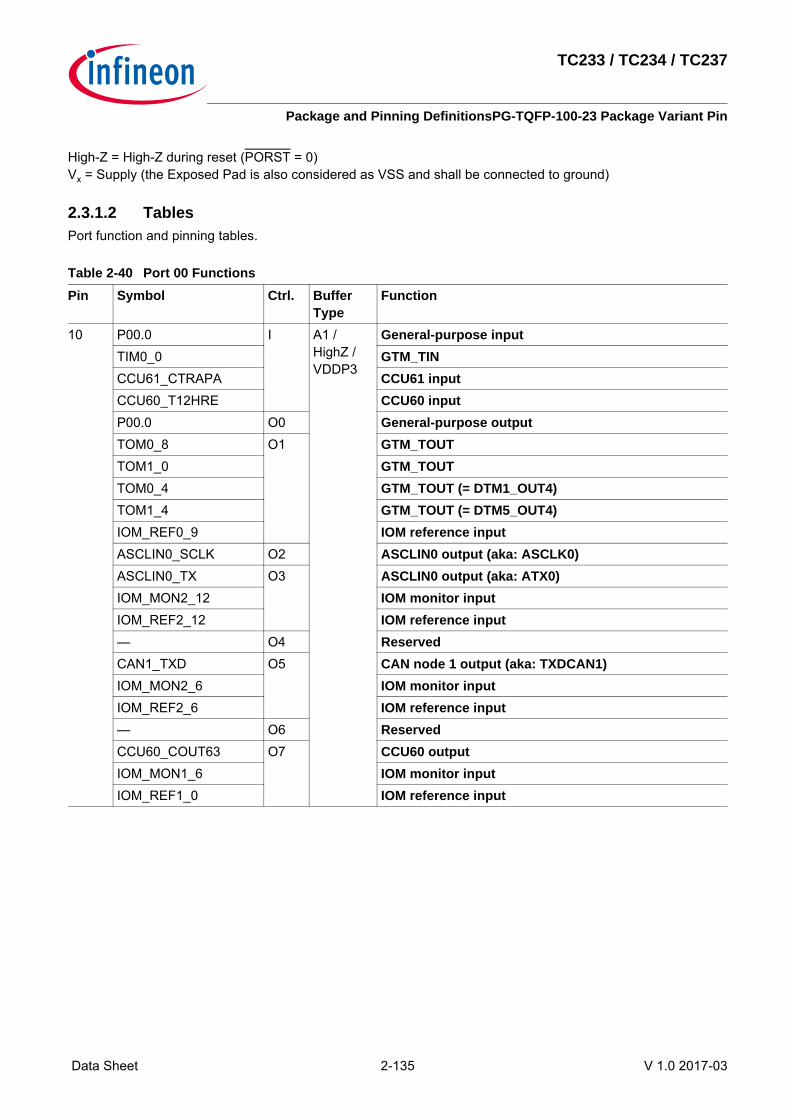
TC233 / TC234 / TC237
Package and Pinning DefinitionsPG-TQFP-100-23 Package Variant Pin
Data Sheet 2-135 V 1.0 2017-03
High-Z = High-Z during reset (PORST = 0)Vx = Supply (the Exposed Pad is also considered as VSS and shall be connected to ground)
2.3.1.2 TablesPort function and pinning tables.
Table 2-40 Port 00 FunctionsPin Symbol Ctrl. Buffer
TypeFunction
10 P00.0 I A1 / HighZ / VDDP3
General-purpose inputTIM0_0 GTM_TINCCU61_CTRAPA CCU61 inputCCU60_T12HRE CCU60 inputP00.0 O0 General-purpose outputTOM0_8 O1 GTM_TOUTTOM1_0 GTM_TOUTTOM0_4 GTM_TOUT (= DTM1_OUT4)TOM1_4 GTM_TOUT (= DTM5_OUT4)IOM_REF0_9 IOM reference inputASCLIN0_SCLK O2 ASCLIN0 output (aka: ASCLK0)ASCLIN0_TX O3 ASCLIN0 output (aka: ATX0)IOM_MON2_12 IOM monitor inputIOM_REF2_12 IOM reference input— O4 ReservedCAN1_TXD O5 CAN node 1 output (aka: TXDCAN1)IOM_MON2_6 IOM monitor inputIOM_REF2_6 IOM reference input— O6 ReservedCCU60_COUT63 O7 CCU60 outputIOM_MON1_6 IOM monitor inputIOM_REF1_0 IOM reference input

TC233 / TC234 / TC237
Package and Pinning DefinitionsPG-TQFP-100-23 Package Variant Pin
Data Sheet 2-136 V 1.0 2017-03
Table 2-41 Port 02 FunctionsPin Symbol Ctrl. Buffer
TypeFunction
1 P02.0 I A1+ / HighZ / VDDP3
General-purpose inputTIM0_0 GTM_TINSCU_REQ6 SCU inputCCU60_CC60INA CCU60 inputCCU61_CC60INB CCU61 inputP02.0 O0 General-purpose outputTOM0_8 O1 GTM_TOUTTOM1_8 GTM_TOUTTOM0_4 GTM_TOUT (= DTM1_OUT4)TOM1_4 GTM_TOUT (= DTM5_OUT4)IOM_REF0_0 IOM reference input— O2 ReservedQSPI3_SLSO1 O3 QSPI3 output (aka: SLSO31)— O4 ReservedCAN0_TXD O5 CAN node 0 output (aka: TXDCAN0)IOM_MON2_5 IOM monitor inputIOM_REF2_5 IOM reference inputERAY0_TXDA O6 ERAY0 outputCCU60_CC60 O7 CCU60 outputIOM_MON1_2 IOM monitor inputIOM_REF1_6 IOM reference input

TC233 / TC234 / TC237
Package and Pinning DefinitionsPG-TQFP-100-23 Package Variant Pin
Data Sheet 2-137 V 1.0 2017-03
2 P02.1 I A1 / HighZ / VDDP3
General-purpose inputTIM0_1 GTM_TINCAN0_RXDA CAN node 0 input (aka: RXDCAN0A)ERAY0_RXDA2 ERAY0 inputSCU_REQ14 SCU inputP02.1 O0 General-purpose outputTOM0_9 O1 GTM_TOUTTOM1_9 GTM_TOUTTOM0_4N GTM_TOUT (= DTM1_OUT4_N)TOM1_4N GTM_TOUT (= DTM5_OUT4_N)IOM_REF0_1 IOM reference input— O2 ReservedQSPI3_SLSO2 O3 QSPI3 output (aka: SLSO32)— O4 Reserved— O5 Reserved— O6 ReservedCCU60_COUT60 O7 CCU60 outputIOM_MON1_3 IOM monitor inputIOM_REF1_3 IOM reference input
Table 2-41 Port 02 Functions (cont’d)
Pin Symbol Ctrl. Buffer Type
Function

TC233 / TC234 / TC237
Package and Pinning DefinitionsPG-TQFP-100-23 Package Variant Pin
Data Sheet 2-138 V 1.0 2017-03
3 P02.2 I A1+ / HighZ / VDDP3
General-purpose inputTIM0_2 GTM_TINCCU60_CC61INA CCU60 inputCCU61_CC61INB CCU61 inputP02.2 O0 General-purpose outputTOM0_10 O1 GTM_TOUTTOM1_10 GTM_TOUTTOM0_5 GTM_TOUT (= DTM1_OUT5)TOM1_5 GTM_TOUT (= DTM5_OUT5)IOM_REF0_2 IOM reference inputASCLIN1_TX O2 ASCLIN1 output (aka: ATX1)IOM_MON2_13 IOM monitor inputIOM_REF2_13 IOM reference inputQSPI3_SLSO3 O3 QSPI3 output (aka: SLSO33)— O4 ReservedCAN2_TXD O5 CAN node 2 output (aka: TXDCAN2)IOM_MON2_7 IOM monitor inputIOM_REF2_7 IOM reference inputERAY0_TXDB O6 ERAY0 outputCCU60_CC61 O7 CCU60 outputIOM_MON1_1 IOM monitor inputIOM_REF1_5 IOM reference input
Table 2-41 Port 02 Functions (cont’d)
Pin Symbol Ctrl. Buffer Type
Function

TC233 / TC234 / TC237
Package and Pinning DefinitionsPG-TQFP-100-23 Package Variant Pin
Data Sheet 2-139 V 1.0 2017-03
4 P02.3 I A1 / HighZ / VDDP3
General-purpose inputTIM0_3 GTM_TINASCLIN1_RXG ASCLIN1 input (aka: ARX1G)CAN2_RXDB CAN node 2 input (aka: RXDCAN2B)ERAY0_RXDB2 ERAY0 inputP02.3 O0 General-purpose outputTOM0_11 O1 GTM_TOUTTOM1_11 GTM_TOUTTOM0_5N GTM_TOUT (= DTM1_OUT5_N)TOM1_5N GTM_TOUT (= DTM5_OUT5_N)IOM_REF0_3 IOM reference input— O2 ReservedQSPI3_SLSO4 O3 QSPI3 output (aka: SLSO34)— O4 Reserved— O5 Reserved— O6 ReservedCCU60_COUT61 O7 CCU60 outputIOM_MON1_4 IOM monitor inputIOM_REF1_2 IOM reference input
Table 2-41 Port 02 Functions (cont’d)
Pin Symbol Ctrl. Buffer Type
Function
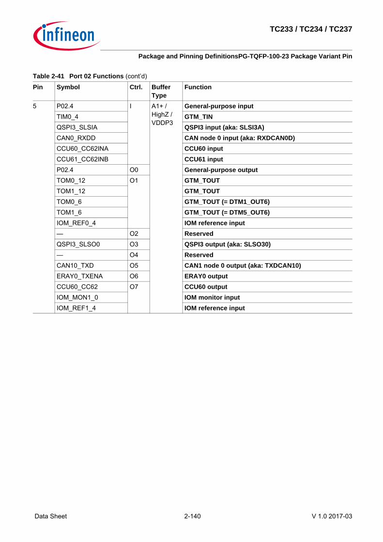
TC233 / TC234 / TC237
Package and Pinning DefinitionsPG-TQFP-100-23 Package Variant Pin
Data Sheet 2-140 V 1.0 2017-03
5 P02.4 I A1+ / HighZ / VDDP3
General-purpose inputTIM0_4 GTM_TINQSPI3_SLSIA QSPI3 input (aka: SLSI3A)CAN0_RXDD CAN node 0 input (aka: RXDCAN0D)CCU60_CC62INA CCU60 inputCCU61_CC62INB CCU61 inputP02.4 O0 General-purpose outputTOM0_12 O1 GTM_TOUTTOM1_12 GTM_TOUTTOM0_6 GTM_TOUT (= DTM1_OUT6)TOM1_6 GTM_TOUT (= DTM5_OUT6)IOM_REF0_4 IOM reference input— O2 ReservedQSPI3_SLSO0 O3 QSPI3 output (aka: SLSO30)— O4 ReservedCAN10_TXD O5 CAN1 node 0 output (aka: TXDCAN10)ERAY0_TXENA O6 ERAY0 outputCCU60_CC62 O7 CCU60 outputIOM_MON1_0 IOM monitor inputIOM_REF1_4 IOM reference input
Table 2-41 Port 02 Functions (cont’d)
Pin Symbol Ctrl. Buffer Type
Function

TC233 / TC234 / TC237
Package and Pinning DefinitionsPG-TQFP-100-23 Package Variant Pin
Data Sheet 2-141 V 1.0 2017-03
6 P02.5 I A1+ / HighZ / VDDP3
General-purpose inputTIM0_5 GTM_TINQSPI3_MRSTA QSPI3 input (aka: MRST3A)SENT_SENT3C SENT inputP02.5 O0 General-purpose outputTOM0_13 O1 GTM_TOUTTOM1_13 GTM_TOUTTOM0_6N GTM_TOUT (= DTM1_OUT6_N)TOM1_6N GTM_TOUT (= DTM5_OUT6_N)IOM_REF0_5 IOM reference inputCAN0_TXD O2 CAN node 0 output (aka: TXDCAN0)IOM_MON2_5 IOM monitor inputIOM_REF2_5 IOM reference inputQSPI3_MRST O3 QSPI3 output (aka: MRST3)IOM_MON2_3 IOM monitor inputIOM_REF2_3 IOM reference input— O4 ReservedCAN11_TXD O5 CAN1 node 1 output (aka: TXDCAN11)ERAY0_TXENB O6 ERAY0 outputCCU60_COUT62 O7 CCU60 outputIOM_MON1_5 IOM monitor inputIOM_REF1_1 IOM reference input
Table 2-41 Port 02 Functions (cont’d)
Pin Symbol Ctrl. Buffer Type
Function

TC233 / TC234 / TC237
Package and Pinning DefinitionsPG-TQFP-100-23 Package Variant Pin
Data Sheet 2-142 V 1.0 2017-03
7 P02.6 I A1 / HighZ / VDDP3
General-purpose inputTIM0_6 GTM_TINQSPI3_MTSRA QSPI3 input (aka: MTSR3A)SENT_SENT2C SENT inputCCU60_CC60INC CCU60 inputCCU60_CCPOS0A CCU60 inputCCU61_T12HRB CCU61 inputGPT120_T3INA GPT120 inputCAN10_RXDF CAN1 node 0 input (aka: RXDCAN10F)P02.6 O0 General-purpose outputTOM0_14 O1 GTM_TOUTTOM1_14 GTM_TOUTTOM0_7 GTM_TOUT (= DTM1_OUT7)TOM1_7 GTM_TOUT (= DTM5_OUT7)IOM_REF0_6 IOM reference input— O2 ReservedQSPI3_MTSR O3 QSPI3 output (aka: MTSR3)— O4 ReservedVADC_EMUX00 O5 VADC output— O6 ReservedCCU60_CC60 O7 CCU60 outputIOM_MON1_2 IOM monitor inputIOM_REF1_6 IOM reference input
Table 2-41 Port 02 Functions (cont’d)
Pin Symbol Ctrl. Buffer Type
Function

TC233 / TC234 / TC237
Package and Pinning DefinitionsPG-TQFP-100-23 Package Variant Pin
Data Sheet 2-143 V 1.0 2017-03
8 P02.7 I A1 / HighZ / VDDP3
General-purpose inputTIM0_7 GTM_TINQSPI3_SCLKA QSPI3 input (aka: SCLK3A)SENT_SENT1C SENT inputCCU60_CC61INC CCU60 inputCCU60_CCPOS1A CCU60 inputCCU61_T13HRB CCU61 inputGPT120_T3EUDA GPT120 inputCAN11_RXDF CAN1 node 1 input (aka: RXDCAN11F)PMU_FDEST PMU inputP02.7 O0 General-purpose outputTOM0_15 O1 GTM_TOUTTOM1_15 GTM_TOUTTOM0_7N GTM_TOUT (= DTM1_OUT7_N)TOM1_7N GTM_TOUT (= DTM5_OUT7_N)IOM_REF0_7 IOM reference input— O2 ReservedQSPI3_SCLK O3 QSPI3 output (aka: SCLK3)— O4 ReservedVADC_EMUX01 O5 VADC outputSENT_SPC1 O6 SENT outputCCU60_CC61 O7 CCU60 outputIOM_MON1_1 IOM monitor inputIOM_REF1_5 IOM reference input
Table 2-41 Port 02 Functions (cont’d)
Pin Symbol Ctrl. Buffer Type
Function

TC233 / TC234 / TC237
Package and Pinning DefinitionsPG-TQFP-100-23 Package Variant Pin
Data Sheet 2-144 V 1.0 2017-03
9 P02.8 I A1 / HighZ / VDDP3
General-purpose inputTIM0_0 GTM_TINSENT_SENT0C SENT inputCCU60_CC62INC CCU60 inputCCU60_CCPOS2A CCU60 inputCCU61_T12HRC CCU61 inputCCU61_T13HRC CCU61 inputGPT120_T4INA GPT120 inputP02.8 O0 General-purpose outputTOM0_8 O1 GTM_TOUTTOM1_0 GTM_TOUTTOM0_4N GTM_TOUT (= DTM1_OUT4_N)TOM1_4N GTM_TOUT (= DTM5_OUT4_N)IOM_REF0_8 IOM reference inputQSPI3_SLSO5 O2 QSPI3 output (aka: SLSO35)— O3 Reserved— O4 ReservedVADC_EMUX02 O5 VADC output— O6 ReservedCCU60_CC62 O7 CCU60 outputIOM_MON1_0 IOM monitor inputIOM_REF1_4 IOM reference input
Table 2-41 Port 02 Functions (cont’d)
Pin Symbol Ctrl. Buffer Type
Function

TC233 / TC234 / TC237
Package and Pinning DefinitionsPG-TQFP-100-23 Package Variant Pin
Data Sheet 2-145 V 1.0 2017-03
Table 2-42 Port 10 FunctionsPin Symbol Ctrl. Buffer
TypeFunction
99 P10.5 I A1 / HighZ / VDDP3
General-purpose inputTIM0_2 GTM_TINSCU_HWCFG4 SCU inputCAN10_RXDA CAN1 node 0 input (aka: RXDCAN10A)P10.5 O0 General-purpose outputTOM0_2 O1 GTM_TOUTTOM1_10 GTM_TOUTIOM_REF2_9 IOM reference input— O2 ReservedQSPI3_SLSO8 O3 QSPI3 output (aka: SLSO38)QSPI1_SLSO9 O4 QSPI1 output (aka: SLSO19)GPT120_T6OUT O5 GPT120 output— O6 Reserved— O7 Reserved
100 P10.6 I A1 / HighZ / VDDP3
General-purpose inputTIM0_3 GTM_TINQSPI3_MTSRB QSPI3 input (aka: MTSR3B)SCU_HWCFG5 SCU inputP10.6 O0 General-purpose outputTOM0_3 O1 GTM_TOUTTOM1_11 GTM_TOUTIOM_REF2_10 IOM reference input— O2 ReservedQSPI3_MTSR O3 QSPI3 output (aka: MTSR3)GPT120_T3OUT O4 GPT120 outputCAN10_TXD O5 CAN1 node 0 output (aka: TXDCAN10)QSPI1_MRST O6 QSPI1 output (aka: MRST1)IOM_MON2_1 IOM monitor inputIOM_REF2_1 IOM reference input— O7 Reserved

TC233 / TC234 / TC237
Package and Pinning DefinitionsPG-TQFP-100-23 Package Variant Pin
Data Sheet 2-146 V 1.0 2017-03
Table 2-43 Port 11 FunctionsPin Symbol Ctrl. Buffer
TypeFunction
91 P11.2 I A1+ / HighZ / VDDP3
General-purpose inputP11.2 O0 General-purpose outputTOM0_8 O1 GTM_TOUTTOM1_1 GTM_TOUTTOM0_4N GTM_TOUT (= DTM1_OUT4_N)TOM1_4N GTM_TOUT (= DTM5_OUT4_N)— O2 ReservedQSPI0_SLSO5 O3 QSPI0 output (aka: SLSO05)QSPI1_SLSO5 O4 QSPI1 output (aka: SLSO15)CCU61_COUT63 O5 CCU61 outputIOM_MON1_7 IOM monitor inputIOM_REF1_7 IOM reference input— O6 ReservedCCU60_COUT63 O7 CCU60 outputIOM_MON1_6 IOM monitor inputIOM_REF1_0 IOM reference input
92 P11.3 I A1+ / HighZ / VDDP3
General-purpose inputQSPI1_MRSTB QSPI1 input (aka: MRST1B)P11.3 O0 General-purpose outputTOM0_10 O1 GTM_TOUTTOM1_2 GTM_TOUTTOM0_5 GTM_TOUT (= DTM1_OUT5)TOM1_5 GTM_TOUT (= DTM5_OUT5)— O2 ReservedQSPI1_MRST O3 QSPI1 output (aka: MRST1)IOM_MON2_1 IOM monitor inputIOM_REF2_1 IOM reference inputERAY0_TXDA O4 ERAY0 outputCCU61_COUT62 O5 CCU61 outputIOM_MON1_13 IOM monitor inputIOM_REF1_8 IOM reference input— O6 ReservedCCU60_COUT62 O7 CCU60 outputIOM_MON1_5 IOM monitor inputIOM_REF1_1 IOM reference input

TC233 / TC234 / TC237
Package and Pinning DefinitionsPG-TQFP-100-23 Package Variant Pin
Data Sheet 2-147 V 1.0 2017-03
93 P11.6 I A1+ / HighZ / VDDP3
General-purpose inputQSPI1_SCLKB QSPI1 input (aka: SCLK1B)P11.6 O0 General-purpose outputTOM0_11 O1 GTM_TOUTTOM1_3 GTM_TOUTTOM0_5N GTM_TOUT (= DTM1_OUT5_N)TOM1_5N GTM_TOUT (= DTM5_OUT5_N)ERAY0_TXENB O2 ERAY0 outputQSPI1_SCLK O3 QSPI1 output (aka: SCLK1)ERAY0_TXENA O4 ERAY0 outputCCU61_COUT61 O5 CCU61 outputIOM_MON1_12 IOM monitor inputIOM_REF1_9 IOM reference input— O6 ReservedCCU60_COUT61 O7 CCU60 outputIOM_MON1_4 IOM monitor inputIOM_REF1_2 IOM reference input
95 P11.8 I A1 / HighZ / VDDP3
General-purpose inputQSPI1_MTSRC QSPI1 input (aka: MTSR1C)P11.8 O0 General-purpose outputTOM0_4 O1 GTM_TOUT (= DTM1_OUT4)TOM1_4 GTM_TOUT (= DTM5_OUT4)— O2 ReservedQSPI1_SLSO10 O3 QSPI1 output (aka: SLSO110)QSPI1_MTSR O4 QSPI1 output (aka: MTSR1)— O5 Reserved— O6 Reserved— O7 Reserved
Table 2-43 Port 11 Functions (cont’d)
Pin Symbol Ctrl. Buffer Type
Function

TC233 / TC234 / TC237
Package and Pinning DefinitionsPG-TQFP-100-23 Package Variant Pin
Data Sheet 2-148 V 1.0 2017-03
94 P11.9 I A1+ / HighZ / VDDP3
General-purpose inputQSPI1_MTSRB QSPI1 input (aka: MTSR1B)ERAY0_RXDA1 ERAY0 inputP11.9 O0 General-purpose outputTOM0_12 O1 GTM_TOUTTOM1_4 GTM_TOUT (= DTM5_OUT4)TOM0_6 GTM_TOUT (= DTM1_OUT6)TOM1_6 GTM_TOUT (= DTM5_OUT6)— O2 ReservedQSPI1_MTSR O3 QSPI1 output (aka: MTSR1)— O4 ReservedCCU61_COUT60 O5 CCU61 outputIOM_MON1_11 IOM monitor inputIOM_REF1_10 IOM reference input— O6 ReservedCCU60_COUT60 O7 CCU60 outputIOM_MON1_3 IOM monitor inputIOM_REF1_3 IOM reference input
96 P11.10 I A1+ / HighZ / VDDP3
General-purpose inputASCLIN1_RXE ASCLIN1 input (aka: ARX1E)ERAY0_RXDB1 ERAY0 inputSCU_REQ12 SCU inputCAN12_RXDD CAN1 node 2 input (aka: RXDCAN12D)P11.10 O0 General-purpose outputTOM0_13 O1 GTM_TOUTTOM1_5 GTM_TOUT (= DTM5_OUT5)TOM0_6N GTM_TOUT (= DTM1_OUT6_N)TOM1_6N GTM_TOUT (= DTM5_OUT6_N)— O2 ReservedQSPI0_SLSO3 O3 QSPI0 output (aka: SLSO03)QSPI1_SLSO3 O4 QSPI1 output (aka: SLSO13)CCU61_CC62 O5 CCU61 outputIOM_MON1_10 IOM monitor inputIOM_REF1_11 IOM reference input— O6 ReservedCCU60_CC62 O7 CCU60 outputIOM_MON1_0 IOM monitor inputIOM_REF1_4 IOM reference input
Table 2-43 Port 11 Functions (cont’d)
Pin Symbol Ctrl. Buffer Type
Function

TC233 / TC234 / TC237
Package and Pinning DefinitionsPG-TQFP-100-23 Package Variant Pin
Data Sheet 2-149 V 1.0 2017-03
97 P11.11 I A1+ / HighZ / VDDP3
General-purpose inputP11.11 O0 General-purpose outputTOM0_14 O1 GTM_TOUTTOM1_6 GTM_TOUT (= DTM5_OUT6)TOM0_7N GTM_TOUT (= DTM1_OUT7_N)TOM1_7N GTM_TOUT (= DTM5_OUT7_N)— O2 ReservedQSPI0_SLSO4 O3 QSPI0 output (aka: SLSO04)QSPI1_SLSO4 O4 QSPI1 output (aka: SLSO14)CCU61_CC61 O5 CCU61 outputIOM_MON1_9 IOM monitor inputIOM_REF1_12 IOM reference inputERAY0_TXENB O6 ERAY0 outputCCU60_CC61 O7 CCU60 outputIOM_MON1_1 IOM monitor inputIOM_REF1_5 IOM reference input
98 P11.12 I A1+ / HighZ / VDDP3
General-purpose inputP11.12 O0 General-purpose outputTOM0_15 O1 GTM_TOUTTOM1_7 GTM_TOUT (= DTM5_OUT7)TOM0_7 GTM_TOUT (= DTM1_OUT7)TOM1_7 GTM_TOUT (= DTM5_OUT7)ASCLIN1_TX O2 ASCLIN1 output (aka: ATX1)IOM_MON2_13 IOM monitor inputIOM_REF2_13 IOM reference inputGTM_CLK2 O3 GTM outputERAY0_TXDB O4 ERAY0 outputCCU61_CC60 O5 CCU61 outputIOM_MON1_8 IOM monitor inputIOM_REF1_13 IOM reference inputSCU_EXTCLK1 O6 SCU outputCCU60_CC60 O7 CCU60 outputIOM_MON1_2 IOM monitor inputIOM_REF1_6 IOM reference input
Table 2-43 Port 11 Functions (cont’d)
Pin Symbol Ctrl. Buffer Type
Function

TC233 / TC234 / TC237
Package and Pinning DefinitionsPG-TQFP-100-23 Package Variant Pin
Data Sheet 2-150 V 1.0 2017-03
Table 2-44 Port 13 FunctionsPin Symbol Ctrl. Buffer
TypeFunction
87 P13.0 I A1 / HighZ / VDDP3
General-purpose inputCCU60_CTRAPA CCU60 inputGPT120_T6EUDB GPT120 inputP13.0 O0 General-purpose outputTOM0_5 O1 GTM_TOUT (= DTM1_OUT5)TOM1_5 GTM_TOUT (= DTM5_OUT5)TOM0_6N GTM_TOUT (= DTM1_OUT6_N)TOM1_6N GTM_TOUT (= DTM5_OUT6_N)— O2 ReservedQSPI2_SCLK O3 QSPI2 output (aka: SCLK2)— O4 Reserved— O5 Reserved— O6 ReservedCAN10_TXD O7 CAN1 node 0 output (aka: TXDCAN10)
88 P13.1 I A1 / HighZ / VDDP3
General-purpose inputCCU60_CCPOS0C CCU60 inputGPT120_T3INB GPT120 inputCAN10_RXDB CAN1 node 0 input (aka: RXDCAN10B)P13.1 O0 General-purpose outputTOM0_6 O1 GTM_TOUT (= DTM1_OUT6)TOM1_6 GTM_TOUT (= DTM5_OUT6)TOM0_7 GTM_TOUT (= DTM1_OUT7)TOM1_7 GTM_TOUT (= DTM5_OUT7)— O2 Reserved— O3 Reserved— O4 Reserved— O5 Reserved— O6 Reserved— O7 Reserved

TC233 / TC234 / TC237
Package and Pinning DefinitionsPG-TQFP-100-23 Package Variant Pin
Data Sheet 2-151 V 1.0 2017-03
89 P13.2 I A1 / HighZ / VDDP3
General-purpose inputCCU60_CCPOS1C CCU60 inputGPT120_T3EUDB GPT120 inputGPT120_CAPINA GPT120 inputP13.2 O0 General-purpose outputTOM0_7 O1 GTM_TOUT (= DTM1_OUT7)TOM1_7 GTM_TOUT (= DTM5_OUT7)TOM0_7N GTM_TOUT (= DTM1_OUT7_N)TOM1_7N GTM_TOUT (= DTM5_OUT7_N)CAN11_TXD O2 CAN1 node 1 output (aka: TXDCAN11)— O3 Reserved— O4 Reserved— O5 Reserved— O6 Reserved— O7 Reserved
90 P13.3 I A1 / HighZ / VDDP3
General-purpose inputCCU60_CCPOS2C CCU60 inputGPT120_T4INB GPT120 inputCAN11_RXDB CAN1 node 1 input (aka: RXDCAN11B)P13.3 O0 General-purpose outputTOM0_8 O1 GTM_TOUTTOM1_0 GTM_TOUTTOM0_4 GTM_TOUT (= DTM1_OUT4)TOM1_4 GTM_TOUT (= DTM5_OUT4)— O2 ReservedQSPI2_MTSR O3 QSPI2 output (aka: MTSR2)— O4 Reserved— O5 Reserved— O6 Reserved— O7 Reserved
Table 2-44 Port 13 Functions (cont’d)
Pin Symbol Ctrl. Buffer Type
Function

TC233 / TC234 / TC237
Package and Pinning DefinitionsPG-TQFP-100-23 Package Variant Pin
Data Sheet 2-152 V 1.0 2017-03
Table 2-45 Port 14 FunctionsPin Symbol Ctrl. Buffer
TypeFunction
81 P14.0 I A1+ / HighZ / VDDP3
General-purpose inputTIM0_3 GTM_TINP14.0 O0 General-purpose outputTOM0_3 O1 GTM_TOUTTOM1_3 GTM_TOUTTOM0_6 GTM_TOUT (= DTM1_OUT6)TOM1_6 GTM_TOUT (= DTM5_OUT6)ASCLIN0_TX O2 ASCLIN0 output (aka: ATX0)IOM_MON2_12 IOM monitor inputIOM_REF2_12 IOM reference inputERAY0_TXDA O3 ERAY0 outputERAY0_TXDB O4 ERAY0 outputCAN1_TXD O5 CAN node 1 output (aka: TXDCAN1)IOM_MON2_6 IOM monitor inputIOM_REF2_6 IOM reference inputASCLIN0_SCLK O6 ASCLIN0 output (aka: ASCLK0)CCU60_COUT62 O7 CCU60 outputIOM_MON1_5 IOM monitor inputIOM_REF1_1 IOM reference input

TC233 / TC234 / TC237
Package and Pinning DefinitionsPG-TQFP-100-23 Package Variant Pin
Data Sheet 2-153 V 1.0 2017-03
82 P14.1 I A1+ / HighZ / VDDP3
General-purpose inputTIM0_4 GTM_TINASCLIN0_RXA ASCLIN0 input (aka: ARX0A)CAN1_RXDB CAN node 1 input (aka: RXDCAN1B)ERAY0_RXDA3 ERAY0 inputSCU_REQ15 SCU inputERAY0_RXDB3 ERAY0 inputSCU_EVRWUPA AI SCU inputP14.1 O0 General-purpose outputTOM0_4 O1 GTM_TOUT (= DTM1_OUT4)TOM1_4 GTM_TOUT (= DTM5_OUT4)TOM0_7 GTM_TOUT (= DTM1_OUT7)TOM1_7 GTM_TOUT (= DTM5_OUT7)IOM_REF1_14 IOM reference inputASCLIN0_TX O2 ASCLIN0 output (aka: ATX0)IOM_MON2_12 IOM monitor inputIOM_REF2_12 IOM reference input— O3 Reserved— O4 Reserved— O5 Reserved— O6 ReservedCCU60_COUT63 O7 CCU60 outputIOM_MON1_6 IOM monitor inputIOM_REF1_0 IOM reference input
83 P14.3 I A1 / PU / VDDP3
General-purpose inputTIM0_6 GTM_TINSCU_REQ10 SCU inputSCU_HWCFG3_BMI SCU inputP14.3 O0 General-purpose outputTOM0_6 O1 GTM_TOUT (= DTM1_OUT6)TOM1_6 GTM_TOUT (= DTM5_OUT6)IOM_REF2_4 IOM reference input— O2 ReservedQSPI2_SLSO3 O3 QSPI2 output (aka: SLSO23)ASCLIN1_SLSO O4 ASCLIN1 output (aka: ASLSO1)— O5 Reserved— O6 Reserved— O7 Reserved
Table 2-45 Port 14 Functions (cont’d)
Pin Symbol Ctrl. Buffer Type
Function

TC233 / TC234 / TC237
Package and Pinning DefinitionsPG-TQFP-100-23 Package Variant Pin
Data Sheet 2-154 V 1.0 2017-03
84 P14.4 I A1+ / HighZ / VDDP3
General-purpose inputTIM0_7 GTM_TINP14.4 O0 General-purpose outputTOM0_7 O1 GTM_TOUT (= DTM1_OUT7)TOM1_7 GTM_TOUT (= DTM5_OUT7)TOM0_7N GTM_TOUT (= DTM1_OUT7_N)TOM1_7N GTM_TOUT (= DTM5_OUT7_N)IOM_REF2_8 IOM reference input— O2 Reserved— O3 Reserved— O4 Reserved— O5 Reserved— O6 Reserved— O7 Reserved
85 P14.6 I A1+ / PU / VDDP3
General-purpose inputTIM0_1 GTM_TINSCU_HWCFG0_DCLDO
SCU input
QSPI0_MRSTD QSPI0 input (aka: MRST0D)P14.6 O0 General-purpose outputTOM0_1 O1 GTM_TOUTTOM1_1 GTM_TOUTIOM_REF2_14 IOM reference input— O2 ReservedQSPI2_SLSO2 O3 QSPI2 output (aka: SLSO22)— O4 Reserved— O5 ReservedERAY0_TXENB O6 ERAY0 output— O7 Reserved
Table 2-45 Port 14 Functions (cont’d)
Pin Symbol Ctrl. Buffer Type
Function

TC233 / TC234 / TC237
Package and Pinning DefinitionsPG-TQFP-100-23 Package Variant Pin
Data Sheet 2-155 V 1.0 2017-03
Table 2-46 Port 15 FunctionsPin Symbol Ctrl. Buffer
TypeFunction
76 P15.0 I A1 / HighZ / VDDP3
General-purpose inputP15.0 O0 General-purpose outputTOM1_3 O1 GTM_TOUTTOM0_11 GTM_TOUTTOM0_7N GTM_TOUT (= DTM1_OUT7_N)TOM1_7N GTM_TOUT (= DTM5_OUT7_N)ASCLIN1_TX O2 ASCLIN1 output (aka: ATX1)IOM_MON2_13 IOM monitor inputIOM_REF2_13 IOM reference inputQSPI0_SLSO13 O3 QSPI0 output (aka: SLSO013)— O4 ReservedCAN2_TXD O5 CAN node 2 output (aka: TXDCAN2)IOM_MON2_7 IOM monitor inputIOM_REF2_7 IOM reference inputASCLIN1_SCLK O6 ASCLIN1 output (aka: ASCLK1)— O7 Reserved
77 P15.1 I A1 / HighZ / VDDP3
General-purpose inputASCLIN1_RXA ASCLIN1 input (aka: ARX1A)QSPI2_SLSIB QSPI2 input (aka: SLSI2B)CAN2_RXDA CAN node 2 input (aka: RXDCAN2A)SCU_REQ16 SCU inputSCU_EVRWUPB AI SCU inputP15.1 O0 General-purpose outputTOM1_4 O1 GTM_TOUT (= DTM5_OUT4)TOM0_12 GTM_TOUTTOM0_4 GTM_TOUT (= DTM1_OUT4)TOM1_4 GTM_TOUT (= DTM5_OUT4)ASCLIN1_TX O2 ASCLIN1 output (aka: ATX1)IOM_MON2_13 IOM monitor inputIOM_REF2_13 IOM reference inputQSPI2_SLSO5 O3 QSPI2 output (aka: SLSO25)— O4 Reserved— O5 Reserved— O6 Reserved— O7 Reserved

TC233 / TC234 / TC237
Package and Pinning DefinitionsPG-TQFP-100-23 Package Variant Pin
Data Sheet 2-156 V 1.0 2017-03
78 P15.2 I A1 / HighZ / VDDP3
General-purpose inputQSPI2_MRSTE QSPI2 input (aka: MRST2E)QSPI2_SLSIA QSPI2 input (aka: SLSI2A)QSPI2_HSICINA QSPI2 input (aka: HSIC2INA)P15.2 O0 General-purpose outputTOM1_5 O1 GTM_TOUT (= DTM5_OUT5)TOM0_13 GTM_TOUTTOM0_4N GTM_TOUT (= DTM1_OUT4_N)TOM1_4N GTM_TOUT (= DTM5_OUT4_N)ASCLIN0_TX O2 ASCLIN0 output (aka: ATX0)IOM_MON2_12 IOM monitor inputIOM_REF2_12 IOM reference inputQSPI2_SLSO0 O3 QSPI2 output (aka: SLSO20)— O4 ReservedCAN1_TXD O5 CAN node 1 output (aka: TXDCAN1)IOM_MON2_6 IOM monitor inputIOM_REF2_6 IOM reference inputASCLIN0_SCLK O6 ASCLIN0 output (aka: ASCLK0)— O7 Reserved
79 P15.3 I A1 / HighZ / VDDP3
General-purpose inputASCLIN0_RXB ASCLIN0 input (aka: ARX0B)QSPI2_SCLKA QSPI2 input (aka: SCLK2A)QSPI2_HSICINB QSPI2 input (aka: HSIC2INB)CAN1_RXDA CAN node 1 input (aka: RXDCAN1A)P15.3 O0 General-purpose outputTOM1_6 O1 GTM_TOUT (= DTM5_OUT6)TOM0_14 GTM_TOUTTOM0_5 GTM_TOUT (= DTM1_OUT5)TOM1_5 GTM_TOUT (= DTM5_OUT5)ASCLIN0_TX O2 ASCLIN0 output (aka: ATX0)IOM_MON2_12 IOM monitor inputIOM_REF2_12 IOM reference inputQSPI2_SCLK O3 QSPI2 output (aka: SCLK2)— O4 Reserved— O5 Reserved— O6 Reserved— O7 Reserved
Table 2-46 Port 15 Functions (cont’d)
Pin Symbol Ctrl. Buffer Type
Function

TC233 / TC234 / TC237
Package and Pinning DefinitionsPG-TQFP-100-23 Package Variant Pin
Data Sheet 2-157 V 1.0 2017-03
80 P15.5 I A1 / HighZ / VDDP3
General-purpose inputASCLIN1_RXB ASCLIN1 input (aka: ARX1B)QSPI2_MTSRA QSPI2 input (aka: MTSR2A)SCU_REQ13 SCU inputP15.5 O0 General-purpose outputTOM0_0 O1 GTM_TOUTTOM1_0 GTM_TOUTTOM0_5N GTM_TOUT (= DTM1_OUT5_N)TOM1_5N GTM_TOUT (= DTM5_OUT5_N)ASCLIN1_TX O2 ASCLIN1 output (aka: ATX1)IOM_MON2_13 IOM monitor inputIOM_REF2_13 IOM reference inputQSPI2_MTSR O3 QSPI2 output (aka: MTSR2)— O4 Reserved— O5 Reserved— O6 ReservedCCU60_CC61 O7 CCU60 outputIOM_MON1_1 IOM monitor inputIOM_REF1_5 IOM reference input
Table 2-47 Port 20 FunctionsPin Symbol Ctrl. Buffer
TypeFunction
64 P20.2 I Input Only / PU / VDDP3
General-purpose inputTESTMODE Factory Test Mode Enable
Table 2-46 Port 15 Functions (cont’d)
Pin Symbol Ctrl. Buffer Type
Function

TC233 / TC234 / TC237
Package and Pinning DefinitionsPG-TQFP-100-23 Package Variant Pin
Data Sheet 2-158 V 1.0 2017-03
69 P20.8 I A1 / HighZ / VDDP3
General-purpose inputTIM0_7 GTM_TINP20.8 O0 General-purpose outputTOM1_7 O1 GTM_TOUT (= DTM5_OUT7)TOM0_7 GTM_TOUT (= DTM1_OUT7)TOM0_4 GTM_TOUT (= DTM1_OUT4)TOM1_4 GTM_TOUT (= DTM5_OUT4)IOM_MON2_8 IOM monitor inputASCLIN1_SLSO O2 ASCLIN1 output (aka: ASLSO1)QSPI0_SLSO0 O3 QSPI0 output (aka: SLSO00)QSPI1_SLSO0 O4 QSPI1 output (aka: SLSO10)CAN0_TXD O5 CAN node 0 output (aka: TXDCAN0)IOM_MON2_5 IOM monitor inputIOM_REF2_5 IOM reference inputSCU_WDT0LCK O6 SCU outputCCU61_CC60 O7 CCU61 outputIOM_MON1_8 IOM monitor inputIOM_REF1_13 IOM reference input
70 P20.9 I A1 / HighZ / VDDP3
General-purpose inputASCLIN1_RXC ASCLIN1 input (aka: ARX1C)QSPI0_SLSIB QSPI0 input (aka: SLSI0B)SCU_REQ11 SCU inputCAN12_RXDE CAN1 node 2 input (aka: RXDCAN12E)P20.9 O0 General-purpose outputTOM1_13 O1 GTM_TOUTTOM0_13 GTM_TOUTTOM0_4N GTM_TOUT (= DTM1_OUT4_N)TOM1_4N GTM_TOUT (= DTM5_OUT4_N)IOM_MON2_11 IOM monitor input— O2 ReservedQSPI0_SLSO1 O3 QSPI0 output (aka: SLSO01)QSPI1_SLSO1 O4 QSPI1 output (aka: SLSO11)— O5 ReservedSCU_WDTSLCK O6 SCU outputCCU61_CC61 O7 CCU61 outputIOM_MON1_9 IOM monitor inputIOM_REF1_12 IOM reference input
Table 2-47 Port 20 Functions (cont’d)
Pin Symbol Ctrl. Buffer Type
Function

TC233 / TC234 / TC237
Package and Pinning DefinitionsPG-TQFP-100-23 Package Variant Pin
Data Sheet 2-159 V 1.0 2017-03
71 P20.10 I A1 / HighZ / VDDP3
General-purpose inputP20.10 O0 General-purpose outputTOM1_14 O1 GTM_TOUTTOM0_14 GTM_TOUTTOM0_5 GTM_TOUT (= DTM1_OUT5)TOM1_5 GTM_TOUT (= DTM5_OUT5)IOM_MON2_14 IOM monitor inputASCLIN1_TX O2 ASCLIN1 output (aka: ATX1)IOM_MON2_13 IOM monitor inputIOM_REF2_13 IOM reference inputQSPI0_SLSO6 O3 QSPI0 output (aka: SLSO06)QSPI2_SLSO7 O4 QSPI2 output (aka: SLSO27)CAN12_TXD O5 CAN1 node 2 output (aka: TXDCAN12)ASCLIN1_SCLK O6 ASCLIN1 output (aka: ASCLK1)CCU61_CC62 O7 CCU61 outputIOM_MON1_10 IOM monitor inputIOM_REF1_11 IOM reference input
72 P20.11 I A1+ / HighZ / VDDP3
General-purpose inputQSPI0_SCLKA QSPI0 input (aka: SCLK0A)P20.11 O0 General-purpose outputTOM1_15 O1 GTM_TOUTTOM0_15 GTM_TOUTTOM0_5N GTM_TOUT (= DTM1_OUT5_N)TOM1_5N GTM_TOUT (= DTM5_OUT5_N)IOM_MON2_15 IOM monitor input— O2 ReservedQSPI0_SCLK O3 QSPI0 output (aka: SCLK0)— O4 ReservedCAN11_TXD O5 CAN1 node 1 output (aka: TXDCAN11)— O6 ReservedCCU61_COUT60 O7 CCU61 outputIOM_MON1_11 IOM monitor inputIOM_REF1_10 IOM reference input
Table 2-47 Port 20 Functions (cont’d)
Pin Symbol Ctrl. Buffer Type
Function

TC233 / TC234 / TC237
Package and Pinning DefinitionsPG-TQFP-100-23 Package Variant Pin
Data Sheet 2-160 V 1.0 2017-03
73 P20.12 I A1 / HighZ / VDDP3
General-purpose inputQSPI0_MRSTA QSPI0 input (aka: MRST0A)CAN11_RXDH CAN1 node 1 input (aka: RXDCAN11H)IOM_PIN13 IOM pad inputP20.12 O0 General-purpose outputTOM1_0 O1 GTM_TOUTTOM0_8 GTM_TOUTTOM0_6 GTM_TOUT (= DTM1_OUT6)TOM1_6 GTM_TOUT (= DTM5_OUT6)IOM_MON0_13 IOM monitor input— O2 ReservedQSPI0_MRST O3 QSPI0 output (aka: MRST0)IOM_MON2_0 IOM monitor inputIOM_REF2_0 IOM reference inputQSPI0_MTSR O4 QSPI0 output (aka: MTSR0)— O5 Reserved— O6 ReservedCCU61_COUT61 O7 CCU61 outputIOM_MON1_12 IOM monitor inputIOM_REF1_9 IOM reference input
74 P20.13 I A1+ / HighZ / VDDP3
General-purpose inputQSPI0_SLSIA QSPI0 input (aka: SLSI0A)CAN12_RXDH CAN1 node 2 input (aka: RXDCAN12H)IOM_PIN14 IOM pad inputP20.13 O0 General-purpose outputTOM1_1 O1 GTM_TOUTTOM0_9 GTM_TOUTTOM0_6N GTM_TOUT (= DTM1_OUT6_N)TOM1_6N GTM_TOUT (= DTM5_OUT6_N)IOM_MON0_14 IOM monitor input— O2 ReservedQSPI0_SLSO2 O3 QSPI0 output (aka: SLSO02)QSPI1_SLSO2 O4 QSPI1 output (aka: SLSO12)QSPI0_SCLK O5 QSPI0 output (aka: SCLK0)— O6 ReservedCCU61_COUT62 O7 CCU61 outputIOM_MON1_13 IOM monitor inputIOM_REF1_8 IOM reference input
Table 2-47 Port 20 Functions (cont’d)
Pin Symbol Ctrl. Buffer Type
Function
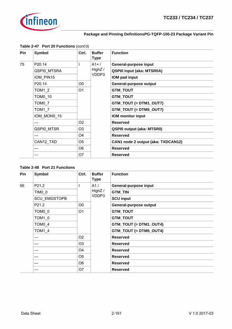
TC233 / TC234 / TC237
Package and Pinning DefinitionsPG-TQFP-100-23 Package Variant Pin
Data Sheet 2-161 V 1.0 2017-03
75 P20.14 I A1+ / HighZ / VDDP3
General-purpose inputQSPI0_MTSRA QSPI0 input (aka: MTSR0A)IOM_PIN15 IOM pad inputP20.14 O0 General-purpose outputTOM1_2 O1 GTM_TOUTTOM0_10 GTM_TOUTTOM0_7 GTM_TOUT (= DTM1_OUT7)TOM1_7 GTM_TOUT (= DTM5_OUT7)IOM_MON0_15 IOM monitor input— O2 ReservedQSPI0_MTSR O3 QSPI0 output (aka: MTSR0)— O4 ReservedCAN12_TXD O5 CAN1 node 2 output (aka: TXDCAN12)— O6 Reserved— O7 Reserved
Table 2-48 Port 21 FunctionsPin Symbol Ctrl. Buffer
TypeFunction
56 P21.2 I A1 / HighZ / VDDP3
General-purpose inputTIM0_0 GTM_TINSCU_EMGSTOPB SCU inputP21.2 O0 General-purpose outputTOM0_0 O1 GTM_TOUTTOM1_0 GTM_TOUTTOM0_4 GTM_TOUT (= DTM1_OUT4)TOM1_4 GTM_TOUT (= DTM5_OUT4)— O2 Reserved— O3 Reserved— O4 Reserved— O5 Reserved— O6 Reserved— O7 Reserved
Table 2-47 Port 20 Functions (cont’d)
Pin Symbol Ctrl. Buffer Type
Function

TC233 / TC234 / TC237
Package and Pinning DefinitionsPG-TQFP-100-23 Package Variant Pin
Data Sheet 2-162 V 1.0 2017-03
57 P21.3 I A1 / HighZ / VDDP3
General-purpose inputTIM0_1 GTM_TINP21.3 O0 General-purpose outputTOM0_1 O1 GTM_TOUTTOM1_1 GTM_TOUTTOM0_4N GTM_TOUT (= DTM1_OUT4_N)TOM1_4N GTM_TOUT (= DTM5_OUT4_N)— O2 Reserved— O3 Reserved— O4 Reserved— O5 Reserved— O6 Reserved— O7 Reserved
58 P21.4 I A1 / HighZ / VDDP3
General-purpose inputTIM0_2 GTM_TINP21.4 O0 General-purpose outputTOM0_2 O1 GTM_TOUTTOM1_2 GTM_TOUTTOM0_5 GTM_TOUT (= DTM1_OUT5)TOM1_5 GTM_TOUT (= DTM5_OUT5)— O2 Reserved— O3 Reserved— O4 Reserved— O5 Reserved— O6 Reserved— O7 Reserved
Table 2-48 Port 21 Functions (cont’d)
Pin Symbol Ctrl. Buffer Type
Function
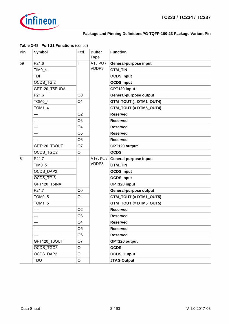
TC233 / TC234 / TC237
Package and Pinning DefinitionsPG-TQFP-100-23 Package Variant Pin
Data Sheet 2-163 V 1.0 2017-03
59 P21.6 I A1 / PU / VDDP3
General-purpose inputTIM0_4 GTM_TINTDI OCDS inputOCDS_TGI2 OCDS inputGPT120_T5EUDA GPT120 inputP21.6 O0 General-purpose outputTOM0_4 O1 GTM_TOUT (= DTM1_OUT4)TOM1_4 GTM_TOUT (= DTM5_OUT4)— O2 Reserved— O3 Reserved— O4 Reserved— O5 Reserved— O6 ReservedGPT120_T3OUT O7 GPT120 outputOCDS_TGO2 O OCDS
61 P21.7 I A1+ / PU / VDDP3
General-purpose inputTIM0_5 GTM_TINOCDS_DAP2 OCDS inputOCDS_TGI3 OCDS inputGPT120_T5INA GPT120 inputP21.7 O0 General-purpose outputTOM0_5 O1 GTM_TOUT (= DTM1_OUT5)TOM1_5 GTM_TOUT (= DTM5_OUT5)— O2 Reserved— O3 Reserved— O4 Reserved— O5 Reserved— O6 ReservedGPT120_T6OUT O7 GPT120 outputOCDS_TGO3 O OCDSOCDS_DAP2 O OCDS OutputTDO O JTAG Output
Table 2-48 Port 21 Functions (cont’d)
Pin Symbol Ctrl. Buffer Type
Function

TC233 / TC234 / TC237
Package and Pinning DefinitionsPG-TQFP-100-23 Package Variant Pin
Data Sheet 2-164 V 1.0 2017-03
Table 2-49 Port 23 FunctionsPin Symbol Ctrl. Buffer
TypeFunction
51 P23.1 I A1+ / HighZ / VDDP3
General-purpose inputTIM0_6 GTM_TINP23.1 O0 General-purpose outputTOM0_6 O1 GTM_TOUT (= DTM1_OUT6)TOM0_15 GTM_TOUTASCLIN1_RTS O2 ASCLIN1 output (aka: ARTS1)QSPI3_SLSO13 O3 QSPI3 output (aka: SLSO313)GTM_CLK0 O4 GTM outputSCU_EXTCLK1 O5 SCU outputSCU_EXTCLK0 O6 SCU output— O7 Reserved
Table 2-50 Port 33 FunctionsPin Symbol Ctrl. Buffer
TypeFunction
41 P33.5 I A1 / HighZ / VDDP3
General-purpose inputTIM0_1 GTM_TINCCU61_CCPOS2C CCU61 inputGPT120_T4EUDB GPT120 inputIOM_PIN5 IOM pad inputP33.5 O0 General-purpose outputTOM0_1 O1 GTM_TOUTTOM1_1 GTM_TOUTTOM0_5 GTM_TOUT (= DTM1_OUT5)TOM1_5 GTM_TOUT (= DTM5_OUT5)IOM_MON0_5 IOM monitor inputQSPI0_SLSO7 O2 QSPI0 output (aka: SLSO07)QSPI1_SLSO7 O3 QSPI1 output (aka: SLSO17)— O4 ReservedVADC_EMUX11 O5 VADC outputVADC_G0BFL1 O6 VADC outputCCU61_CC60 O7 CCU61 outputIOM_MON1_8 IOM monitor inputIOM_REF1_13 IOM reference input

TC233 / TC234 / TC237
Package and Pinning DefinitionsPG-TQFP-100-23 Package Variant Pin
Data Sheet 2-165 V 1.0 2017-03
42 P33.6 I A1 / HighZ / VDDP3
General-purpose inputTIM0_2 GTM_TINASCLIN1_RXF ASCLIN1 input (aka: ARX1F)CCU61_CCPOS1C CCU61 inputGPT120_T2EUDB GPT120 inputCAN10_RXDH CAN1 node 0 input (aka: RXDCAN10H)IOM_PIN6 IOM pad inputP33.6 O0 General-purpose outputTOM0_2 O1 GTM_TOUTTOM1_2 GTM_TOUTTOM0_5N GTM_TOUT (= DTM1_OUT5_N)TOM1_5N GTM_TOUT (= DTM5_OUT5_N)IOM_MON0_6 IOM monitor input— O2 Reserved— O3 ReservedASCLIN1_TX O4 ASCLIN1 output (aka: ATX1)IOM_MON2_13 IOM monitor inputIOM_REF2_13 IOM reference inputVADC_EMUX10 O5 VADC outputVADC_G0BFL2 O6 VADC outputCCU61_CC61 O7 CCU61 outputIOM_MON1_9 IOM monitor inputIOM_REF1_12 IOM reference inputHSM_HSM1 O HSM output
Table 2-50 Port 33 Functions (cont’d)
Pin Symbol Ctrl. Buffer Type
Function

TC233 / TC234 / TC237
Package and Pinning DefinitionsPG-TQFP-100-23 Package Variant Pin
Data Sheet 2-166 V 1.0 2017-03
43 P33.7 I A1+ / HighZ / VDDP3
General-purpose inputTIM0_3 GTM_TINCAN0_RXDE CAN node 0 input (aka: RXDCAN0E)SCU_REQ8 SCU inputCCU61_CCPOS0C CCU61 inputGPT120_T2INB GPT120 inputIOM_PIN7 IOM pad inputP33.7 O0 General-purpose outputTOM0_3 O1 GTM_TOUTTOM1_3 GTM_TOUTTOM0_6 GTM_TOUT (= DTM1_OUT6)TOM1_6 GTM_TOUT (= DTM5_OUT6)IOM_MON0_7 IOM monitor input— O2 ReservedQSPI3_SLSO7 O3 QSPI3 output (aka: SLSO37)— O4 ReservedCAN10_TXD O5 CAN1 node 0 output (aka: TXDCAN10)VADC_G0BFL3 O6 VADC outputCCU61_COUT60 O7 CCU61 outputIOM_MON1_11 IOM monitor inputIOM_REF1_10 IOM reference inputHSM_HSM2 O HSM output
Table 2-50 Port 33 Functions (cont’d)
Pin Symbol Ctrl. Buffer Type
Function

TC233 / TC234 / TC237
Package and Pinning DefinitionsPG-TQFP-100-23 Package Variant Pin
Data Sheet 2-167 V 1.0 2017-03
44 P33.8 I A1+ / HighZ / VDDP3
General-purpose inputTIM0_4 GTM_TINSCU_EMGSTOPA SCU inputIOM_PIN8 IOM pad inputP33.8 O0 General-purpose outputTOM0_4 O1 GTM_TOUT (= DTM1_OUT4)TOM1_4 GTM_TOUT (= DTM5_OUT4)TOM0_6N GTM_TOUT (= DTM1_OUT6_N)TOM1_6N GTM_TOUT (= DTM5_OUT6_N)IOM_MON0_8 IOM monitor input— O2 ReservedQSPI3_SLSO2 O3 QSPI3 output (aka: SLSO32)— O4 ReservedCAN0_TXD O5 CAN node 0 output (aka: TXDCAN0)IOM_MON2_5 IOM monitor inputIOM_REF2_5 IOM reference input— O6 ReservedCCU61_COUT62 O7 CCU61 outputIOM_MON1_13 IOM monitor inputIOM_REF1_8 IOM reference inputSMU_FSP O SMU
Table 2-50 Port 33 Functions (cont’d)
Pin Symbol Ctrl. Buffer Type
Function

TC233 / TC234 / TC237
Package and Pinning DefinitionsPG-TQFP-100-23 Package Variant Pin
Data Sheet 2-168 V 1.0 2017-03
45 P33.9 I A1 / HighZ / VDDP3
General-purpose inputTIM0_1 GTM_TINQSPI3_HSICINA QSPI3 input (aka: HSIC3INA)IOM_PIN9 IOM pad inputP33.9 O0 General-purpose outputTOM0_1 O1 GTM_TOUTTOM1_1 GTM_TOUTTOM0_7 GTM_TOUT (= DTM1_OUT7)TOM1_7 GTM_TOUT (= DTM5_OUT7)IOM_MON0_9 IOM monitor input— O2 ReservedQSPI3_SLSO1 O3 QSPI3 output (aka: SLSO31)— O4 Reserved— O5 Reserved— O6 ReservedCCU61_CC62 O7 CCU61 outputIOM_MON1_10 IOM monitor inputIOM_REF1_11 IOM reference input
46 P33.10 I A1+ / HighZ / VDDP3
General-purpose inputTIM0_0 GTM_TINQSPI3_SLSIC QSPI3 input (aka: SLSI3C)QSPI3_HSICINB QSPI3 input (aka: HSIC3INB)IOM_PIN10 IOM pad inputP33.10 O0 General-purpose outputTOM0_0 O1 GTM_TOUTTOM1_0 GTM_TOUTTOM0_7N GTM_TOUT (= DTM1_OUT7_N)TOM1_7N GTM_TOUT (= DTM5_OUT7_N)IOM_MON0_10 IOM monitor inputQSPI1_SLSO6 O2 QSPI1 output (aka: SLSO16)QSPI3_SLSO11 O3 QSPI3 output (aka: SLSO311)ASCLIN1_SLSO O4 ASCLIN1 output (aka: ASLSO1)GTM_CLK1 O5 GTM outputSCU_EXTCLK1 O6 SCU outputCCU61_COUT61 O7 CCU61 outputIOM_MON1_12 IOM monitor inputIOM_REF1_9 IOM reference input
Table 2-50 Port 33 Functions (cont’d)
Pin Symbol Ctrl. Buffer Type
Function

TC233 / TC234 / TC237
Package and Pinning DefinitionsPG-TQFP-100-23 Package Variant Pin
Data Sheet 2-169 V 1.0 2017-03
Table 2-51 Port 40 FunctionsPin Symbol Ctrl. Buffer
TypeFunction
40 P40.0 I S / VDDM General-purpose inputVADCG0_0 AI VADC input channel 0 of group 0
39 P40.1 I S / VDDM General-purpose inputVADCG0_1 AI VADC input channel 1 of group 0
(with multiplexer diagnostics)38 P40.2 I S / VDDM General-purpose input
VADCG0_2 AI VADC input channel 2 of group 0(with multiplexer diagnostics)
37 P40.3 I S / VDDM General-purpose inputVADCG0_3 AI VADC input channel 3 of group 0
36 P40.4 I S / VDDM General-purpose inputVADCG0_4 AI VADC input channel 4 of group 0
35 P40.5 I S / VDDM General-purpose inputVADCG0_5 AI VADC input channel 5 of group 0
34 P40.6 I S / VDDM General-purpose inputVADCG0_6 AI VADC input channel 6 of group 0
29 P40.7 I S / VDDM General-purpose inputVADCG0_7 AI VADC input channel 7 of group 0
(with pull down diagnostics)28 P40.8 I S / VDDM General-purpose input
VADCG0_8 AI VADC input channel 8 of group 027 P40.9 I S / VDDM General-purpose input
VADCG0_9 AI VADC input channel 9 of group 0(with multiplexer diagnostics)
26 P40.10 I S / VDDM General-purpose inputVADCG0_10 AI VADC input channel 10 of group 0
(with multiplexer diagnostics)25 P40.11 I S / VDDM General-purpose input
SENT_SENT0A SENT inputCCU60_CCPOS0D CCU60 inputVADCG0_11 AI VADC input channel 11 of group 0

TC233 / TC234 / TC237
Package and Pinning DefinitionsPG-TQFP-100-23 Package Variant Pin
Data Sheet 2-170 V 1.0 2017-03
Table 2-52 Port 41 FunctionsPin Symbol Ctrl. Buffer
TypeFunction
24 P41.0 I S / VDDM General-purpose inputSENT_SENT1A SENT inputCCU60_CCPOS1B CCU60 inputVADCG1_0 AI VADC input channel 0 of group 1
23 P41.1 I S / VDDM General-purpose inputVADCG1_1 AI VADC input channel 1 of group 1
(with multiplexer diagnostics)22 P41.2 I S / VDDM General-purpose input
SENT_SENT2A SENT inputCCU61_CCPOS1B CCU61 inputVADCG1_2 AI VADC input channel 2 of group 1
(with multiplexer diagnostics)21 P41.3 I S / VDDM General-purpose input
SENT_SENT3A SENT inputCCU61_CCPOS1D CCU61 inputVADCG1_3 AI VADC input channel 3 of group 1
(with pull down diagnostics)20 P41.4 I S / VDDM General-purpose input
VADCG1_4 AI VADC input channel 4 of group 119 P41.5 I S / VDDM General-purpose input
VADCG1_5 AI VADC input channel 5 of group 118 P41.6 I S / VDDM General-purpose input
VADCG1_6 AI VADC input channel 6 of group 117 P41.7 I S / VDDM General-purpose input
VADCG1_7 AI VADC input channel 7 of group 116 P41.8 I S / VDDM General-purpose input
VADCG1_8 AI VADC input channel 8 of group 115 P41.9 I S / VDDM General-purpose input
VADCG1_9 AI VADC input channel 9 of group 1(with multiplexer diagnostics)
14 P41.10 I S / VDDM General-purpose inputVADCG1_10 AI VADC input channel 10 of group 1
(with multiplexer diagnostics)13 P41.11 I S / VDDM General-purpose input
VADCG1_11 AI VADC input channel 11 of group 1

TC233 / TC234 / TC237
Package and Pinning DefinitionsPG-TQFP-100-23 Package Variant Pin
Data Sheet 2-171 V 1.0 2017-03
Table 2-53 System I/OPin Symbol Ctrl. Buffer
TypeFunction
53 XTAL1 I VDDP3 Main Oscillator/PLL/Clock Generator Input54 XTAL2 O VDDP3 Main Oscillator/PLL/Clock Generator Output60 TMS/DAP1 I A1+ / PD /
VDDP3Debug Interface
DAP1 I/O Device Access Port LIne 162 TRST I Input Only
/ PD / VDDP3
JTAG Module Reset/Enable Input
63 TCK/DAP0 I Input Only / PD / VDDP3
OCDS inputDAP0 I Device Access Port LIne 0
65 ESR1 I/O A1+ / PU / VDDP3
SCU inputEVRWUP I EVR Wakeup Pin
66 PORST I Input Only / PD / VDDP3
Power On ResetAdditional strong PD in case of power fail.
67 ESR0 I/O A1+ / OD / VDDP3
SCU input/outputEVRWUP I EVR Wakeup Pin
Table 2-54 SupplyPin Symbol Ctrl. Buffer
TypeFunction
30 VAGND I — Negative Analog Reference Voltage 031 VAREF I — Positive Analog Reference Voltage 086 VDDP3 I — Digital I/O Power Supply (3.3V)
This pin supplies also the Flash 3.3V.47 VDDP3 I — Digital I/O Power Supply (3.3V)48 VDD I — Digital Core Power Supply (1.3V)
Output of EVR13.52 VDD I — Digital Core Power Supply (1.3V)
This pin supplies also the main XTAL Oscillator/PLL (1.3V). A higher decoupling capacitor is therefore recommended to the VSS pin for better noise immunity.
55 VDDP3 I — Digital I/O Power Supply (3.3V)This pin supplies also the main XTAL Oscillator/PLL (3.3V). A higher decoupling capacitor is therefore recommended to the VSS pin for better noise immunity.
33 VDDM I — ADC Power Supply (5.0V)12 VDDP3 I — Digital I/O Power Supply (3.3V)11 VDD I — Digital Core Power Supply (1.3V)

TC233 / TC234 / TC237
Package and Pinning DefinitionsPG-TQFP-100-23 Package Variant Pin
Data Sheet 2-172 V 1.0 2017-03
2.3.2 Pull-Up/Pull-Down Reset Behavior of the Pins
68 VDD I — Digital Core Power Supply (1.3V)32 VSSM I — Analog Ground for VDDM
Table 2-55 List of Pull-Up/Pull-Down Reset Behavior of the PinsPins PORST = 0 PORST = 1all GPIOs High-ZTDI, TESTMODE Pull-upPORST1)
1) Pull-down with IPORST relevant is always activated when a primary supply monitor detects a violation.
Pull-down with IPORST relevant Pull-down with IPDLI relevantTRST, TCK, TMS Pull-downESR0 The open-drain driver is used to
drive low.2)
2) Valid additionally after deactivation of PORST until the internal reset phase has finished. See the SCU chapter for details.
Pull-up3)
3) See the SCU_IOCR register description.
ESR1 Pull-up3)
P14.2, P14.3, P14.6 Pull-upP21.7 / TDO Pull-up High-Z/Pull-up4)
4) Depends on JTAG/DAP selection with TRST.
Table 2-54 Supply (cont’d)
Pin Symbol Ctrl. Buffer Type
Function

TC233 / TC234 / TC237
Electrical SpecificationParameter Interpretation
Data Sheet 3-173 V 1.0 2017-03
3 Electrical Specification
3.1 Parameter InterpretationThe parameters listed in this section partly represent the characteristics of the TC233 / TC234 / TC237 and partlyits requirements on the system. To aid interpreting the parameters easily when evaluating them for a design, theyare marked with an two-letter abbreviation in column “Symbol”:• CC
Such parameters indicate Controller Characteristics which are a distinctive feature of the TC233 / TC234 / TC237 and must be regarded for a system design.
• SRSuch parameters indicate System Requirements which must provided by the microcontroller system in which the TC233 / TC234 / TC237 designed in.

TC233 / TC234 / TC237
Electrical SpecificationAbsolute Maximum Ratings
Data Sheet 3-174 V 1.0 2017-03
3.2 Absolute Maximum RatingsStresses above the values listed under “Absolute Maximum Ratings” may cause permanent damage to the device.This is a stress rating only and functional operation of the device at these or any other conditions above thoseindicated in the Operational Conditions of this specification is not implied. Exposure to absolute maximum ratingconditions may affect device reliability.
Table 3-1 Absolute Maximum RatingsParameter Symbol Values Unit Note / Test Condition
Min. Typ. Max.Storage Temperature TST SR -65 - 170 °C upto 65h @ TJ =
150°C; upto 15h @ TJ = 170°C
Voltage at VDD power supply pins with respect to VSS 1)
1) Valid for cumulated for up to 2.8h and pulse forms following a power supply switch on phase, where the rise and fall times are releated to the system capacities and coils.
VDD SR - - 1.9 V
Voltage at VDDP3 power supply pins with respect to VSS
VDDP3 SR - - 4.43 V
Voltage at VDDM power supply pin with respect to VSS
VDDM SR - - 7.0 V
Voltage on all analog and class S input pins with respect to VSS 2)
2) Voltages below VINmin have no Impact to the device reliabiltiy as Long as the times and currents defined in section Pin Reliability in Overload for the affected pad(s) are not violated.
VIN SR -0.5 - 7.0 V
Voltage on all other input pins with respect to VSS 1)2)
VIN SR -0.5 - min( VDDP3 + 0.6 , 4.23 )
V Whatever is lower
Input current on any pin during overload condition 3)
3) This parameter is an Absolute Maximum Rating. Exposure to Absolute Maximum Ratings for extended periods of time may damage the device.
IIN SR -10 - 10 mA
Absolute maximum sum of all input circuit currents during overload condition 3)
ΣIIN SR -100 - 100 mA

TC233 / TC234 / TC237
Electrical SpecificationPin Reliability in Overload
Data Sheet 3-175 V 1.0 2017-03
3.3 Pin Reliability in OverloadWhen receiving signals from higher voltage devices, low-voltage devices experience overload currents andvoltages that go beyond their own IO power supplies specification.The following table defines overload conditions that will not cause any negative reliability impact if all the followingconditions are met:• full operation life-time is not exceeded• Operating Conditions are met for
– pad supply levels– temperature
• Parameters defined in Absolute Maximum Ratings are not violatedIf a pin current is out of the Operating Conditions but within the overload parameters, then the parametersfunctionality of this pin as stated in the Operating Conditions can no longer be guaranteed. Operation is stillpossible in most cases but with relaxed parameters.Note: An overload condition on one or more pins does not require a reset.
Table 3-2 Overload ParametersParameter Symbol Values Unit Note / Test Condition
Min. Typ. Max.Input current on any digital pin during overload condition
IIN -5 - 5 mA
Input current on analog input pin during overload condition
IINANA -1 - 3 mA-5 - 5 mA limited to 60h over
lifetimeAbsolute sum of all ADC inputs during overload condition
IINSCA -20 - 20 mA
Absolute maximum sum of all input circuit currents during overload condition
ΣIINS -100 - 100 mA
Inactive device pin current during overload condtion 1)
IID -1 - 1 mA All power supply voltages VDDx = 0
Sum of all inactive device pin currents 1)
IIDS -100 - 100 mA
Overload coupling factor for digital inputs, negative 2)
KOVDN CC - - 1.5*10-3 Overload injected on GPIO pad and affecting neighbor GPIO pad
Overload coupling factor for digital inputs, positive 2)
KOVDP CC - - 1*10-5 Overload injected on GPIO pad and affecting neighbor GPIO pad
Overload coupling factor for analog inputs, negative
KOVAN CC - - 1*10-3 Analog Inputs overlaid with pull down diagnostics
- - 1*10-4 else

TC233 / TC234 / TC237
Electrical SpecificationPin Reliability in Overload
Data Sheet 3-176 V 1.0 2017-03
Overload coupling factor for analog inputs, positive
KOVAP CC - - 1*10-4 Analog Inputs overlaid with pull down diagnostics
- - 1*10-5 else1) Limitations for time and supply levels specified in this section are not valid for this parameter.2) Overload is measured as increase of pad leakage caused by injection on neighbor pad.
Table 3-3 PN-Junction Characteristics for positive OverloadPad Type IIN = 3 mA IIN = 5 mAA1 / A1+ UIN = VDDP3 + 0.5 V UIN = VDDP3 + 0.6 VD UIN = VDDM + 0.75 V -
Table 3-4 PN-Junction Characteristics for negative OverloadPad Type IIN = -3 mA IIN = -5 mAA1 / A1+ UIN = VSS - 0.5 V UIN = VSS - 0.6 VD UIN = VSS - 0.75 V -
Table 3-2 Overload Parameters (cont’d)
Parameter Symbol Values Unit Note / Test ConditionMin. Typ. Max.

TC233 / TC234 / TC237
Electrical SpecificationOperating Conditions
Data Sheet 3-177 V 1.0 2017-03
3.4 Operating ConditionsThe following operating conditions must not be exceeded in order to ensure correct operation and reliability of theTC233 / TC234 / TC237. All parameters specified in the following tables refer to these operating conditions, unlessotherwise noticed.Digital supply voltages applied to the TC233 / TC234 / TC237 must be static regulated voltages.All parameters specified in the following tables refer to these operating conditions (see table below), unlessotherwise noticed in the Note / Test Condition column.
Table 3-5 Operating ConditionsParameter Symbol Values Unit Note / Test Condition
Min. Typ. Max.SRI frequency fSRI SR - - 200 MHz
- - 133 MHz vaild only for SAK-TC233LC-24F133F
Max System Frequency fMAX SR - - 200 MHz- - 133 MHz vaild only for SAK-
TC233LC-24F133FCPU0 Frequency fCPU0 SR - - 200 MHz
- - 133 MHz vaild only for SAK-TC233LC-24F133F
PLL output frequency fPLL SR 20 - 200 MHz- - 133 MHz vaild only for SAK-
TC233LC-24F133FPLL_ERAY output frequency fPLLERAY SR 20 - 160 MHz
- - 80 MHz vaild only for SAK-TC233LC-24F133F
SPB frequency fSPB SR - - 100 MHzASCLIN fast frequency fASCLINF SR - - 200 MHz
- - 133 MHz vaild only for SAK-TC233LC-24F133F
ASCLIN slow frequency fASCLINS SR - - 100 MHzBaud2 frequency fBAUD2 SR - - 200 MHz
- - 133 MHz vaild only for SAK-TC233LC-24F133F
FSI2 frequency fFSI2 SR - - 200 MHz- - 133 MHz vaild only for SAK-
TC233LC-24F133FFSI frequency fFSI SR - - 100 MHzGTM frequency fGTM SR - - 100 MHzSTM frequency fSTM SR - - 100 MHzERAY frequency fERAY SR - - 80 MHzBBB frequency fBBB SR - - 100 MHzMultiCAN frequency fCAN SR - - 100 MHz

TC233 / TC234 / TC237
Electrical SpecificationOperating Conditions
Data Sheet 3-178 V 1.0 2017-03
Absolute sum of short circuit currents of the device
ΣISC_D SR - - 100 mA
Ambient Temperature TA SR -40 - 125 °C valid for all SAK products
-40 - 150 °C valid for all SAL products
Junction Temperature TJ SR -40 - 150 °C valid for all SAK products
-40 - 165 °C valid for all SAL products
Core Supply Voltage 1) VDD SR 1.17 1.3 1.43 2) V Only required if externally supplied
ADC analog supply voltage VDDM SR 2.97 5.0 5.5 3) VDigital ground voltage VSS SR 0 - - VAnalog ground voltage for VDDM VSSM CC -0.1 0 0.1 VVoltage to ensure defined pad states 4)
VDDPPA CC 0.72 - - V
Digital supply voltage for GPIO pads and EVR 5)
VDDP3 SR 2.97 3.3 3.63 V
1) No external inductive load permissible if EVR is used. All VDD pins shall be connected together externally on the PCB.2) Voltage overshoot to 1.69V is permissible, provided the duration is less than 2h cumulated. Reduced ADC accuracy and
leakage is increased.3) Voltage overshoot to 6.5V is permissible, provided the duration is less than 2h cumulated. Reduced ADC accuracy and
leakage is increased. 4) This parameter is valid under the assumption the PORST signal is constantly at low level during the power-up/power-down
of VDDP3.5) All VDDP3 pins shall be connected together externally on the PCB.
Table 3-5 Operating Conditions (cont’d)
Parameter Symbol Values Unit Note / Test ConditionMin. Typ. Max.

TC233 / TC234 / TC237
Electrical Specification3.3 V Pads
Data Sheet 3-179 V 1.0 2017-03
3.5 3.3 V Pads
Table 3-6 Standard PadsParameter Symbol Values Unit Note / Test Condition
Min. Typ. Max.Pin capacitance (digital inputs/outputs)
CIO CC - 6 10 pF
Spike filter always blocked pulse duration
tSF1 CC - - 80 ns PORST only
Spike filter pass-through pulse duration
tSF2 CC 220 - - ns PORST only
PORST pad output current 1)
1) Pull-down with IPORST relevant is always activated when a primary supply monitor detects a violation.
IPORST CC 10.1 - - mA VDDP3 = 3.0V; VPORST = 0.9V; TJ = 150°C;
Table 3-7 Class_A1Parameter Symbol Values Unit Note / Test Condition
Min. Typ. Max.Input frequency fIN SR - - 100 MHzInput Hysteresis A1 HYSA1 CC 0.1 *
VDDP3 - - V else
Input Leakage Current Class A1
IOZA1 CC -400 - 400 nA (0.1*VDDP3) < VIN < (0.9*VDDP3)
-475 - 475 nA (0.1*VDDP3) < VIN < (0.9*VDDP3); only vaild for P0.0
-800 - 800 nA elsePull-down current class A1 pads
IPDLA1 CC - - |120| µA VIHmin
|15| - - µA VILmax
Pull-up current class A1 pads IPUHA1 CC |15| - - µA VIHmin
- - |120| µA VILmax
On-Resistance of the A1 pad, medium driver
RDSONA1M CC
50 125 200 Ohm IOH=2mA; IOL=2mA
On-Resistance of the class A1 pad, weak driver
RDSONA1W CC
250 500 800 Ohm IOH=0.5mA; IOL=0.5mA
Input high voltage class A1 pads
VIHA1 CC 0.7 * VDDP3
- - V CMOS
Input low voltage, class A1 pads
VILA1 CC - - 0.3 * VDDP3
V CMOS

TC233 / TC234 / TC237
Electrical Specification3.3 V Pads
Data Sheet 3-180 V 1.0 2017-03
Rise/fall time 1) tA1 CC - - 10+0.4 * CL
ns CL≤100pF; pin out driver=medium
- - 30+2.0 * CL
ns CL≤100pF; pin out driver=weak
1) Rise / fall times are defined 10% - 90% of VDDP3.
Table 3-8 Class_A1+Parameter Symbol Values Unit Note / Test Condition
Min. Typ. Max.Input frequency fIN SR - - 75 MHzInput Leakage Current Class A1+
IOZA1+ CC -1 - 1 µA (0.1*VDDP3) < VIN < (0.9*VDDP3)
-2 - 2 µA elsePull-down current class A1+ pads
IPDLA1+ CC - - |120| µA VIHmin
|15| - - µA VILmax
Pull-up current class A1+ pads IPUHA1+ CC |15| - - µA VIHmin
- - |120| µA VILmax
On-Resistance of the A1+ pad, medium driver
RDSONA1+M CC
50 125 200 Ohm IOH=2mA; IOL=2mA
On-Resistance of the A1+ pad, strong driver
RDSONA1+S CC
10 40 65 Ohm IOH=6mA; IOL=6mA
On-Resistance of the A1+ pad, weak driver
RDSONA1+W CC
250 500 800 Ohm IOH=0.5mA; IOL=0.5mA
Input high voltage, Class A1+ pads
VIHA1+ CC 0.7 * VDDP3
- - V CMOS
Input low voltage Class A1+ pads
VILA1+ CC - - 0.3 * VDDP3
V CMOS
Rise/fall time 1)
1) Rise / fall times are defined 10% - 90% of VDDP3.
tA1+ CC - - 8+0.14 * CL
ns CL≤100pF; edge=slow ; pin out driver=strong (sw)
- - 1+0.14 * CL
ns CL≤100pF; edge=soft ; pin out driver=strong (sf)
- - 10+0.4 * CL
ns CL≤100pF; pin out driver=medium
- - 30+2.0 * CL
ns CL≤100pF; pin out driver=weak
Input Hysteresis A1+ HYSA1+ CC
0.1 * VDDP3
- - V else
Table 3-7 Class_A1 (cont’d)
Parameter Symbol Values Unit Note / Test ConditionMin. Typ. Max.

TC233 / TC234 / TC237
Electrical Specification3.3 V Pads
Data Sheet 3-181 V 1.0 2017-03
Table 3-9 Class_SParameter Symbol Values Unit Note / Test Condition
Min. Typ. Max.Input frequency fIN SR - - 75 MHzInput Hysteresis for S pad 1)
1) Hysteresis is implemented to avoid metastable states and switching due to internal ground bounce. It can't be guaranteed that it suppresses switching due to external system noise.
HYSS CC 0.3 - - VPull-up current for S pad IPUHS CC |11| - - µA VIHmin
- - |120| µA VILmax
Pull-down current for S pad IPDLS CC - - |120| µA VIHmin
|30| - - µA VILmax
Input Leakage current Class S IOZS CC -350 - 350 nA Analog Inputs overlaid with pull down diagnosis
-150 - 150 nA elseInput voltage high for S pad VIHS SR - - 3.8 2)
2) VILx = 0.65 * VDDM
VInput voltage low for S pad VILS SR 1.39 3)
3) VILx = 0.41 * VDDM
- - VInput low threshold variation for S pad 4)
4) VILSD is implemented to ensure J2716 specification. For details of dedicated pins please see AP32286 for details.
VILSD SR -50 - 50 mV max. variation of 1ms; VDDM=constant
Input capacitance for S pad CINS CC - - 10 pFPad set-up time for S pad tSETS CC - - 100 ns
Table 3-10 Class I Parameter Symbol Values Unit Note / Test Condition
Min. Typ. Max.Input frequency fIN SR - - 100 MHzInput Hysteresis for I pad 1) HYSI CC 0.1 *
VDDP3 - - V
Pull-up current for I pad IPUHI CC |15| - - µA VIHImin
- - |120| µA VILImax
Pull-down current for I pad IPDLI CC - - |120| µA VIHImin
|15| - - µA VILImax
Input Leakage Current for I pad IOZI CC -150 - 150 nA (0.1*VDDP3) < VIN < (0.9*VDDP3)
-500 - 350 nA elseInput high voltage for I pad VIHI SR 0.7 *
VDDP3 - - V CMOS

TC233 / TC234 / TC237
Electrical Specification3.3 V Pads
Data Sheet 3-182 V 1.0 2017-03
Input low voltage for I pad VILI SR - - 0.3 * VDDP3
V CMOS
Pad set-up time for I pad tSETI CC - - 100 ns1) Hysteresis is implemented to avoid metastable states and switching due to internal ground bounce. It can't be guaranteed
that it suppresses switching due to external system noise.
Table 3-11 Driver Mode Selection for A1 PadsPDx.2 PDx.1 PDx.0 Port Functionality Driver SettingX X 0 Speed grade 1 medium (A1m)X X 1 Speed grade 2 weak (A1w)
Table 3-12 Driver Mode Selection for A1+ PadsPDx.2 PDx.1 PDx.0 Port Functionality Driver SettingX 0 0 Speed grade 1 Strong soft edge (A1+sf)X 0 1 Speed grade 2 Strong slow edge (A1+sw)X 1 0 Speed grade 3 medium (A1+m)X 1 1 Speed grade 4 weak (A1+w)
Table 3-10 Class I (cont’d)
Parameter Symbol Values Unit Note / Test ConditionMin. Typ. Max.
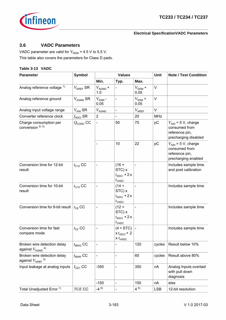
TC233 / TC234 / TC237
Electrical SpecificationVADC Parameters
Data Sheet 3-183 V 1.0 2017-03
3.6 VADC ParametersVADC parameter are valid for VDDM = 4.5 V to 5.5 V.This table also covers the parameters for Class D pads.
Table 3-13 VADCParameter Symbol Values Unit Note / Test Condition
Min. Typ. Max.Analog reference voltage 1) VAREF SR VAGND +
1.0 - VDDM +
0.05 V
Analog reference ground VAGND SR VSSM - 0.05
- VSSM + 0.05
V
Analog input voltage range VAIN SR VAGND - VAREF VConverter reference clock fADCI SR 2 - 20 MHzCharge consumption per conversion 2) 3)
QCONV CC - 50 75 pC VAIN = 5 V, charge consumed from reference pin, precharging disabled
- 10 22 pC VAIN = 5 V, charge consumed from reference pin, precharging enabled
Conversion time for 12-bit result
tC12 CC - (16 + STC) x tADCI + 2 x tVADC
- Includes sample time and post calibration
Conversion time for 10-bit result
tC10 CC - (14 + STC) x tADCI + 2 x tVADC
- Includes sample time
Conversion time for 8-bit result tC8 CC - (12 + STC) x tADCI + 2 x tVADC
- Includes sample time
Conversion time for fast compare mode
tCF CC - (4 + STC) x tADCI + 2 x tVADC
- Includes sample time
Broken wire detection delay against VAGND 4)
tBWG CC - - 120 cycles Result below 10%
Broken wire detection delay against VAREF 5)
tBWR CC - - 60 cycles Result above 80%
Input leakage at analog inputs IOZ1 CC -350 - 350 nA Analog Inputs overlaid with pull down diagnosis
-150 - 150 nA elseTotal Unadjusted Error 1) TUE CC -4 6) - 4 6) LSB 12-bit resolution

TC233 / TC234 / TC237
Electrical SpecificationVADC Parameters
Data Sheet 3-184 V 1.0 2017-03
INL Error EAINL CC -3 - 3 LSB 12-bit resolutionGain Error 1) EAGAIN CC -3.5 - 3.5 LSB 12-bit resolutionDNL error 1) EADNL CC -3 - 3 LSB 12-bit resolutionOffset Error 1) EAOFF CC -4 - 4 LSB 12-bit resolutionTotal capacitance of an analog input
CAINT CC - - 30 pF
Switched capacitance of an analog input
CAINS CC 2 - 7 pF
Resistance of the analog input path
RAIN CC - - 1.5 kOhm
Switched capacitance of a reference input
CAREFS CC - - 30 pF
RMS Noise 7) ENRMS CC - 0.5 0.8 6)8) LSBPositive reference VAREFx pin leakage
IOZ2 CC -2 - 2 µA VAREFx = VAREF; TJ>150°C
-1 - 1 µA VAREFx = VAREF; TJ≤150°C
Negative reference VAGNDx pin leakage
IOZ3 CC -2.5 - 2.5 µA VAGNDx = VAGND; TJ>150°C
-1.5 - 1.5 µA VAGNDx = VAGND; TJ≤150°C
Resistance of the reference input path
RAREF CC - - 1 kOhm
CSD resistance 9) RCSD CC - - 28 kOhmResistance of the multiplexer diagnostics pull-down device
RMDD CC 25 + 1*VIN - 35 - 8*VIN kOhm 0 V ≤ VIN ≤ 2.5 V-5 + 13*VIN
- 15 + 16*VIN
kOhm 2.5 V ≤ VIN ≤ VDDM
Resistance of the multiplexer diagnostics pull-up device
RMDU CC 45 - 6*VIN - 90 - 16*VIN
kOhm 0 V ≥ VIN ≤ 2.5 V
40 - 4*VIN - 65 - 6*VIN kOhm 2.5 V ≤ VIN ≤ VDDM
Resistance of the pull-down test device 10)
RPDD CC - - 0.3 kOhm
CSD voltage accuracy 11) 12) dVCSD CC - - 10 %Wakeup time tWU CC - - 12 µs1) If the reference voltage is reduced by the factor k (k < 1), TUE,DNL,INL,Gain, and Offset errors increase also by the factor
1/k. VAREF must be decoupled with an external capacitor.2) For QCONV = X pC and a conversion time of 1 µs a rms value of X µA results for IAREFx.3) For the details of the mapping for a VADC group to pin VAREFx please see the User's Manual.4) The broken wire detection delay against VAGND is measured in numbers of consecutive precharge cycles at a conversion
rate higher than 1 conversion per 500 ms.5) The broken wire detection delay against VAREF is measured in numbers of consecutive precharge cycles at a conversion
rate higher than 1 conversion per 10 ms. This function is influenced by leakage current, in particular at high temperature.
Table 3-13 VADC (cont’d)
Parameter Symbol Values Unit Note / Test ConditionMin. Typ. Max.

TC233 / TC234 / TC237
Electrical SpecificationVADC Parameters
Data Sheet 3-185 V 1.0 2017-03
VADC parameter are valid for VDDM = 2.97 V to 4.5 V.
6) Resulting worst case combined error is arithmetic combination of TUE and ENRMS.7) This parameter is valid for soldered devices and requires careful analog board design.8) Value is defined for one sigma Gauss distribution.9) In order to avoid an additional error due to incomplete sampling, the sampling time shall be set greater than 5 * RCSD * CAINS.10) The pull-down resistor RPDD is connected between the input pad and the analog multiplexer. The input pad
itself adds another 200-Ohm series resistance, when measuring through the pin.11) CSD: Converter Self Diagnostics, for details please consult the User's Manual.12) Note, that in case CSD voltage is chosen to nom. 1/3 or 2/3 of VAREF voltage, the reference voltage is loaded with a current
of max. VAREF / 45 kOhm.
Table 3-14 VADC_33Parameter Symbol Values Unit Note / Test Condition
Min. Typ. Max.Analog reference voltage 1) VAREF SR VAGND +
1.0 - VDDM +
0.05 V
Analog reference ground VAGND SR VSSM - 0.05
- VSSM + 0.05
V
Analog input voltage range VAIN SR VAGND - VAREF VConverter reference clock fADCI SR 2 - 20 MHzCharge consumption per conversion 2) 3)
QCONV CC - 35 50 pC VAIN = 3.3 V, charge consumed from reference pin, precharging disabled
- 8 17 pC VAIN = 3.3 V, charge consumed from reference pin, precharging enabled
Conversion time for 12-bit result
tC12 CC - (16 + STC) x tADCI + 2 x tVADC
- Includes sample time and post calibration
Conversion time for 10-bit result
tC10 CC - (14 + STC) x tADCI + 2 x tVADC
- Includes sample time
Conversion time for 8-bit result tC8 CC - (12 + STC) x tADCI + 2 x tVADC
- Includes sample time
Conversion time for fast compare mode
tCF CC - (4 + STC) x tADCI + 2 x tVADC
- Includes sample time
Broken wire detection delay against VAGND 4)
tBWG CC - - 120 cycles Result below 10%

TC233 / TC234 / TC237
Electrical SpecificationVADC Parameters
Data Sheet 3-186 V 1.0 2017-03
Broken wire detection delay against VAREF 5)
tBWR CC - - 60 cycles Result above 80%
Input leakage at analog inputs IOZ1 CC -350 - 350 nA Analog Inputs overlaid with pull down diagnostics
-150 - 150 nA elseTotal Unadjusted Error 1) TUE CC -12 - 12 LSB 12-bit Resolution; TJ >
150 °C-6 - 6 LSB 12-bit Resolution; TJ ≤
150 °CINL Error EAINL CC -12 - 12 LSB 12-bit Resolution; TJ >
150 °C-5 - 5 LSB 12-bit Resolution; TJ ≤
150 °CGain Error 1) EAGAIN CC -6 - 6 LSB 12-bit Resolution; TJ >
150 °C-5.5 - 5.5 LSB 12-bit Resolution; TJ ≤
150 °CDNL error 1) EADNL CC -4 - 4 LSB 12-bit resolutionOffset Error 1) EAOFF CC -6 - 6 LSB 12-bit Resolution; TJ >
150 °C-5 - 5 LSB 12-bit Resolution; TJ ≤
150 °CTotal capacitance of an analog input
CAINT CC - - 30 pF
Switched capacitance of an analog input
CAINS CC 2 4 7 pF
Resistance of the analog input path
RAIN CC - - 4.5 kOhm
Switched capacitance of a reference input
CAREFS CC - - 30 pF
RMS Noise 6) ENRMS CC - - 1.7 LSBPositive reference VAREFx pin leakage
IOZ2 CC -2 - 2 µA VAREFx = VAREF; TJ>150°C
-1 - 1 µA VAREFx = VAREF; TJ≤150°C
Negative reference VAGNDx pin leakage
IOZ3 CC -2.5 - 2.5 µA VAGNDx = VAGND; TJ>150°C
-1 - 1 µA VAGNDx = VAGND; TJ≤150°C
Resistance of the reference input path
RAREF CC - - 3 kOhm
Table 3-14 VADC_33 (cont’d)
Parameter Symbol Values Unit Note / Test ConditionMin. Typ. Max.

TC233 / TC234 / TC237
Electrical SpecificationVADC Parameters
Data Sheet 3-187 V 1.0 2017-03
Figure 3-1 Equivalent Circuitry for Analog Inputs
CSD resistance 7) RCSD CC - - 28 kOhmResistance of the multiplexer diagnostics pull-down device
RMDD CC 25 + 3*VIN - 40 + 12*VIN
kOhm 0 V ≤ VIN ≤ 1.667 V
0 + 18*VIN - 0 + 18*VIN kOhm 1.667 V ≤ VIN ≤ VDDM
Resistance of the multiplexer diagnostics pull-up device
RMDU CC 60 - 12*VIN
- 120 - 30*VIN
kOhm 0 V ≤ VIN ≤ 1.667 V
55 - 9*VIN - 95 - 15*VIN
kOhm 1.667 V ≤ VIN ≤ VDDM
Resistance of the pull-down test device 8)
RPDD CC - - 0.9 kOhm
CSD voltage accuracy 9) 10) dVCSD CC - - 10 %Wakeup time tWU CC - - 12 µs1) If the reference voltage is reduced by the factor k (k < 1), TUE,DNL,INL,Gain, and Offset errors increase also by the factor
1/k. VAREF must be decoupled with an external capacitor.2) For QCONV = X pC and a conversion time of 1 µs a rms value of X µA results for IAREFx.3) For the details of the mapping for a VADC group to pin VAREFx please see the User's Manual.4) The broken wire detection delay against VAGND is measured in numbers of consecutive precharge cycles at a conversion
rate higher than 1 conversion per 500 ms.5) The broken wire detection delay against VAREF is measured in numbers of consecutive precharge cycles at a conversion
rate higher than 1 conversion per 10 ms. This function is influenced by leakage current, in particular at high temperature.6) This parameter is valid for soldered devices and requires careful analog board design.7) In order to avoid an additional error due to incomplete sampling, the sampling time shall be set greater than 5 * RCSD * CAINS.8) The pull-down resistor RPDD is connected between the input pad and the analog multiplexer. The input pad
itself adds another 200-Ohm series resistance, when measuring through the pin.9) CSD: Converter Self Diagnostics, for details please consult the User's Manual.10) Note, that in case CSD voltage is chosen to nom. 1/3 or 2/3 of VAREF voltage, the reference voltage is loaded with a current
of max. VAREF / 45 kOhm.
Table 3-14 VADC_33 (cont’d)
Parameter Symbol Values Unit Note / Test ConditionMin. Typ. Max.
A/D Converter
MCS05570
RSource
VAIN CExt CAINT CAINS-
RAIN, On
CAINS

TC233 / TC234 / TC237
Electrical SpecificationMHz Oscillator
Data Sheet 3-188 V 1.0 2017-03
3.7 MHz OscillatorOSC_XTAL is used as accurate and exact clock source. OSC_XTAL supports 8 MHz to 40 MHz crystals externaloutside of the device. Support of ceramic resonators is also provided.
Note: It is strongly recommended to measure the oscillation allowance (negative resistance) in the final target system (layout) to determine the optimal parameters for the oscillator operation. Please refer to the limits specified by the crystal or ceramic resonator supplier.
Table 3-15 OSC_XTALParameter Symbol Values Unit Note / Test Condition
Min. Typ. Max.Input current at XTAL1 IIX1 CC -25 - 25 µA VIN>0V; VIN<VDDP3VOscillator frequency fOSC SR 4 - 40 MHz Direct Input Mode
selected8 - 40 MHz External Crystal Mode
selectedOscillator start-up time 1)
1) tOSCS is defined from the moment when VDDP3 = 3.13V until the oscillations reach an amplitude at XTAL1 of 0.3 * VDDP3. The external oscillator circuitry must be optimized by the customer and checked for negative resistance as recommended and specified by crystal suppliers.
tOSCS CC - - 5 2)
2) This value depends on the frequency of the used external crystal. For faster crystal frequencies this value decrease.
msInput high voltage at XTAL1 VIHBX SR 0.8 - VDDP3 +
0.5 V If shaper is bypassed
Input low voltage at XTAL1 VILBX SR -0.5 - 0.4 V If shaper is bypassedInput voltage at XTAL1 VIX SR -0.5 - VDDP3 +
0.5 V If shaper is not
bypassedInput amplitude (peak to peak) at XTAL1
VPPX SR 0.3 * VDDP3
- VDDP3 + 1.0
V If shaper is not bypassed; fOSC > 25MHz
0.4 * VDDP3
- VDDP3 + 1.0
V If shaper is not bypassed; fOSC ≤ 25MHz

TC233 / TC234 / TC237
Electrical SpecificationBack-up Clock
Data Sheet 3-189 V 1.0 2017-03
3.8 Back-up ClockThe back-up clock provides an alternative clock source.
Table 3-16 Back-up ClockParameter Symbol Values Unit Note / Test Condition
Min. Typ. Max.Back-up clock before trimming fBACKUT CC 75 100 125 MHzSlow speed Back-up clock fBACKSS CC 75 100 125 kHzBack-up clock after trimming fBACKT CC 97.5 100 102.5 MHz

TC233 / TC234 / TC237
Electrical SpecificationTemperature Sensor
Data Sheet 3-190 V 1.0 2017-03
3.9 Temperature Sensor
The following formula calculates the temperature measured by the DTS in [oC] from the RESULT bit field of theDTSSTAT register.
(3.1)
Table 3-17 DTSParameter Symbol Values Unit Note / Test Condition
Min. Typ. Max.Measurement time tM CC - - 100 µsCalibration reference accuracy TCALACC CC -1 - 1 °C calibration points @
TJ=-40°C and TJ=127°C
Non-linearity accuracy over temperature range
TNL CC -2 - 2 °C
Temperature sensor range TSR SR -40 - 170 °CStart-up time after resets inactive
tTSST SR - - 20 µs
Tj DTSSTATRESULT 607( )–2 13,
----------------------------------------------------------------------------=

TC233 / TC234 / TC237
Electrical SpecificationPower Supply Current
Data Sheet 3-191 V 1.0 2017-03
3.10 Power Supply CurrentThe total power supply current defined below consists of leakage and switching component.Application relevant values are typically lower than those given in the following table and depend on the customer'ssystem operating conditions (e.g. thermal connection or used application configurations).The operating conditions for the parameters in the following table are:The real (realisic) power pattern defines the following conditions:• TJ = 150 °C• fSRI = fMAX = fCPU0 = 200 MHz• fSPB = fSTM = fGTM = fBAUD1 = fBAUD2 = fASCLIN = 40 MHz• VDD = 1.326 V• VDDP3 = 3.366 V• VDDM = 5.1 V• core is active• the following peripherals are inactive: HSM, Ethernet, and MTUThe max power pattern defines the following conditions:• TJ = 150 °C• fSRI = fMAX = fCPU0 = 200 MHz• fSPB = fSTM = fGTM = fBAUD1 = fBAUD2 = fASCLIN = 100 MHz• VDD = 1.43 V• VDDP3 = 3.63 V• VDDM = 5.5 V• core is active• all peripherals are active
Table 3-18 Power SupplyParameter Symbol Values Unit Note / Test Condition
Min. Typ. Max.∑ Sum of IDD 1.3 V core and peripheral supply currents
IDD CC - - 215 1) mA valid for Feature Package L, LC, LP, S, and SP; max power pattern
- - 160 mA valid for Feature Package L, LC, LP, S, and SP; real power pattern

TC233 / TC234 / TC237
Electrical SpecificationPower Supply Current
Data Sheet 3-192 V 1.0 2017-03
IDD core current during active power-on reset (PORST held low)
IDDPORST CC
- - 85 mA valid for Feature Package L, LC, LP, S, and SP; TJ=165°C
- - 60 mA valid for Feature Package L, LC, LP, S, and SP; TJ=150°C
- - 40 mA valid for Feature Package L, LC, LP, S, and SP; TJ=125°C
IDD core current of CPU0 lockstep core active
IDDC01 CC - - 34 mA real power pattern
IDD core current added by HSM IDDHSM CC - - 20 mA HSM running at 100MHz.
IDD core current added by FFT IDDFFT CC - - 40 mA FFT running at 200MHz
∑ Sum of 3.3 V supply currents without pad activity
IDDx3RAIL CC - - 34 2) mA real power pattern; incl. OSC, EVR and Pflash read current
- - 44 mA incl. OSC, EVR, Pflash read and Pflash programming current.
IDDM supply current IDDM CC - - 6 mA max pattern; current for 2x VADC modules.
Σ Sum of all currents with DC-DC EVR13 regulator active 3)
IDDTOTDC3 CC
- - 129 mA real power pattern; VDDP3 = 3.3V
∑ Sum of all currents (incl. IDDP3RAIL+IDD+IDDM)
IDDTOTL CC - - 200 mA valid for Feature Package L, LC, LP, S, and SP; real power pattern
∑ Sum of all currents (STANDBY mode)
IEVRSB CC - - 150 4) µA Standby RAM is active. Power to remaining domains switched off. TJ = 25°C; VEVRSB = 5V
∑ Sum of all currents (SLEEP mode)
ISLEEP CC - - 10 mA CPU is in idle, All peripherals in sleep, fSRI/SPB = 1 MHz; TJ = 55°C
Table 3-18 Power Supply (cont’d)
Parameter Symbol Values Unit Note / Test ConditionMin. Typ. Max.

TC233 / TC234 / TC237
Electrical SpecificationPower Supply Current
Data Sheet 3-193 V 1.0 2017-03
3.10.1 Calculating the 1.3 V Current ConsumptionThe current consumption of the 1.3 V rail compose out of two parts:• Static current consumption• Dynamic current consumptionThe static current consumption is related to the device temperature TJ and the dynamic current consumptiondepends of the configured clocking frequencies and the software application executed. These two parts needs tobe added in order to get the rail current consumption.Valid for Feature Package L, LC, LP, S, and SP products:
(3.2)
(3.3)
Function 2 defines the typical static current consumption and Function 3 defines the maximum static currentconsumption. Both functions are valid for VDD = 1.326 V.
Maximum power dissipation PD CC - - 460 mW valid for Feature Package L, LC, LP, S, and SP; max power pattern
- - 360 5) mW valid for Feature Package L, LC, LP, S, and SP; real power pattern
1) It shall be ensured when using the SC DC DC EVR13 that the current is limited to the maximum value documented in the EVR section. EVR SRCSCDC Interrupt shall be kept active to indicate violations of max current and temperature shall be monitored to keep leakage current within limits.
2) Realistic Pflash read pattern with 50% Pflash bandwidth utlilization and a code mix of 50% 0s and 50% 1s. Dynamic Flash Idle via FCON.IDLE is activated bringing a benefit of 4 mA. A decoupling capacitor of atleast 100nF is used. Dflash read current is also included. In TC23x, separate VDDFL3 pin is not available, so only the total VDDx3RAIL is measured and characterized.
3) The total current drawn from external regulator is estimated with 72% EVR13 SMPS regulator Efficiency. IDDTOTDCx is calculated from IDDTOT using the scaled core current [(IDD x VDD)/(VinxEfficiency)] and constitutes all other rail currents and IDDM.
4) The current during STANDBY mode is drawn at VDDP3 supply pin. During RUN-STANDBY mode transition the current drawn at VDDP3 supply pin is less than 6mA.
5) Incase of EVR13 SCDCDC mode, 50 mW need to be additionally added for the real pattern usecase considering 72% SCDCDC efficiency. Incase of EVR13 LDO mode, 320 mW need to be additionally added to consider the pass device power drop out.
Table 3-18 Power Supply (cont’d)
Parameter Symbol Values Unit Note / Test ConditionMin. Typ. Max.
I0 1 2092 mAC
---------, e0 01792, TJ×× C[ ]=
I0 3 196 mAC
---------, e0 01982, TJ×× C[ ]=

TC233 / TC234 / TC237
Electrical SpecificationPower-up and Power-down
Data Sheet 3-194 V 1.0 2017-03
3.11 Power-up and Power-down
Figure 3-2 Single Supply mode - 3.3 V single supply
EVR13 Ramp-up Phase
T0
1
T1
2
T2
0 3
T3Firmware ExecutionBasic Supply & Clock
InfrastructureUser Code Execution
0 V
1.30 V
VDD (internally generated
by EVR13)
1.17 V Primary Reset Threshold
1.33 V
Power Ramp-down phase
4
fCPU=100 MHz default on firmware exit
T4
Startup_Diag_4 v 0.1
PORST (output )
PORST (input )
0 V
3.30 V3.63 V
2.97 V
Primary Reset Threshold
VDDP3 (externally supplied )

TC233 / TC234 / TC237
Electrical SpecificationPower-up and Power-down
Data Sheet 3-195 V 1.0 2017-03
3.11.1 Single Supply mode 3.3 V single supply mode. 1.3 V is generated internally by the EVR13 regulator.• The rate at which current is drawn from the external regulator (dIEXT /dt) is limited during the basic
infrastructure and EVR13 regulator start-up phase (T0 upto T2) to a maximum of 100 mA/100 us. EVR13 is also robust against a voltage ramp-up starting from a residual voltage between 0 - 1 V. Start-up slew rates for supply rails should comply to datasheet values.
• Furthermore it is also ensured that the current drawn from the external regulator (dIEXT /dt) is limited during the Firmware start-up phase (T2 upto T3) to a maximum of 100 mA/100 us.
• PORST is active/ asserted when either PORST (input) or PORST (output) is active/ asserted.• PORST (input) active means that the reset is held active by external agents by pulling the PORST pin low. It
is recommended to keep the PORST (input) asserted until the external supply is above the respective primary reset threshold.
• PORST (output) active means that µC asserts the reset internally and drives the PORST pin low thus propagating the reset to external devices. The PORST (output) is asserted by the µC when atleast one among the two supply domains (1.3 V or 3.3 V) violate their primary under-voltage reset thresholds.The PORST (output) is deasserted by the µC when all supplies are above their primary reset thresholds and the basic supply and clock infrastructure is available.
• The power sequence as shown in Figure 3-2 is enumerated below– T1 refers to the point in time when basic supply and clock infrastructure is available as the external supply
ramps up. The supply mode is evaluated based on the HWCFG[0,2] pins and consequently a soft start of EVR13 regulator is initiated.
– T2 refers to the point in time when all supplies are above their primary reset thresholds. EVR13 regulator has ramped up. PORST (output) is deasserted and HWCFG[3:5] pins are latched on PORST rising edge. Firmware execution is initiated.
– T3 refers to the point in time when Firmware execution is completed. User code execution starts with a default frequency of 100 MHz.
– T4 refers to the point in time during the Ramp-down phase when atleast one of the externally provided or generated supplies (1.3 V or 3.3 V) drop below their respective primary under-voltage reset thresholds.

TC233 / TC234 / TC237
Electrical SpecificationPower-up and Power-down
Data Sheet 3-196 V 1.0 2017-03
Figure 3-3 External Supply mode - 3.3 V and 1.3 V external supply
VDDP3 (externally supplied ) 1 20
0 V
1.30 V
VDD (externally supplied)
1.17 V Primary Reset Threshold
1.33 V
3
T0 T2Firmware ExecutionBasic Supply & Clock
InfrastructureUser Code Execution Power Ramp -down phasefCPU=100 MHz default on firmware exit
T3
Startup_Diag_5 v 0.1
T1
PORST (output )
PORST (input)
0 V
3.30 V3.63 V
2.97 V
Primary Reset Threshold

TC233 / TC234 / TC237
Electrical SpecificationPower-up and Power-down
Data Sheet 3-197 V 1.0 2017-03
3.11.2 External Supply mode All supplies, namely 3.3 V & 1.3 V, are externally supplied.• External supplies VDDP3 & VDD may ramp-up or ramp-down independent of each other with regards to start,
rise and fall time(s). The supply system is also robust against a voltage ramp-up starting from a residual voltage between 0 - 1 V. Start-up slew rates for supply rails should comply to datasheet values.
• The rate at which current is drawn from the external regulator (dIEXT /dt, dIDD /dt) is limited in the Start-up phase to a maximum of 50 mA/100 us.
• PORST is active/ asserted when either PORST (input) or PORST (output) is active/ asserted.• PORST (input) active means that the reset is held active by external agents by pulling the PORST pin low. It
is recommended to keep the PORST (input) asserted until all the external supplies are above their primary reset thresholds.
• PORST (output) active means that µC asserts the reset internally and drives the PORST pin low thus propagating the reset to external devices. The PORST (output) is asserted by the µC when atleast one among the two supply domains (1.3 V or 3.3 V) violate their primary under-voltage reset thresholds.The PORST (output) is deasserted by the µC when all supplies are above their primary reset thresholds and the basic supply and clock infrastructure is available.
• The power sequence as shown in Figure 3-3 is enumerated below– T1 refers to the point in time when all supplies are above their primary reset thresholds and basic clock
infrastructure is available. The supply mode is evaluated based on the HWCFG[0,2] pins. PORST (output) is deasserted and HWCFG[3:5] pins are latched on PORST rising edge. Firmware execution is initiated.
– T2 refers to the point in time when Firmware execution is completed. User code execution starts with a default frequency of 100 MHz.
– T3 refers to the point in time during the Ramp-down phase when atleast one of the externally provided supplies (1.3 V or 3.3 V) drop below their respective primary under-voltage reset thresholds.

TC233 / TC234 / TC237
Electrical SpecificationReset Timing
Data Sheet 3-198 V 1.0 2017-03
3.12 Reset Timing
Table 3-19 Reset TimingsParameter Symbol Values Unit Note / Test Condition
Min. Typ. Max.Application Reset Boot Time 1)
1) The duration of the boot time is defined between the rising edge of the internal application reset and the clock cycle when the first user instruction has entered the CPU pipeline and its processing starts.
tB CC - - 350 µs operating with max. frequencies
System Reset Boot Time tBS CC - - 1 msPower on Reset Boot Time 2)
2) The duration of the boot time is defined by all external supply voltages are inside there operation condictions and the clock cycle when the first user instruction has entered the CPU pipeline and its processing starts.
tBP CC - - 2.5 ms dV/dT=1V/ms. including EVR ramp-up and Firmware execution time
- - 1.1 ms Firmware execution time; without EVR operation (external supply only)
EVR start-up or ramp-up time tEVRstartup CC
- - 1 ms dV/dT=1V/ms
Minimum PORST active hold time after power supplies are stable at operating levels 3)
3) The regulator that supplies VEXT should ensure that VEXT is in the operational region before PORST is externally released by the regulator. Incase of 5V nominal supply, it should be ensured that VEXT > 4V before PORST is released. Incase of 3.3V nominal supply , it should be ensured that VEXT > 3V before PORST is released. The additional minimum PORST hold time is required as an additional mechanism to avoid consecutive PORST toggling owing to slow supply slopes or residual supply ramp-ups. It is also required to activate external PORST atleast 100us before power-fail is recognised to avoid consecutive PORST toggling on a power fail event.
tPOA CC 1 - - ms
HWCFG pins hold time from ESR0 rising edge
tHDH CC 16 / fSPB - - ns
HWCFG pins setup time to ESR0 rising edge
tHDS CC 0 - - ns
Ports inactive after ESR0 reset active
tPI CC - - 8/fSPB ns
Ports inactive after PORST reset active 4)
4) This parameter includes the delay of the analog spike filter in the PORST pad.
tPIP CC - - 150 ns
Hold time from PORST rising edge
tPOH SR 150 - - ns
Setup time to PORST rising edge
tPOS SR 0 - - ns

TC233 / TC234 / TC237
Electrical SpecificationReset Timing
Data Sheet 3-199 V 1.0 2017-03
Figure 3-4 Power, Pad and Reset Timingreset_beh_aurix
VDDP
PORST
PadsPad-state
undefined
VDD
VDDPPA VDDPPA
Pad-state
undefined
VDDPR
Programmed Z / HTristate Z / pullup H
tPOAtPOA
HWCFG
ESR0
tPIP
Z / H
Cold Warm
t HDH
TESTMODE
t P OS t POH
t POS tP OHTRST
t P I
Programmed Programmed
tP I
power -on config
t HDA t HDH
config
t HDA t HDH
config

TC233 / TC234 / TC237
Electrical SpecificationEVR
Data Sheet 3-200 V 1.0 2017-03
3.13 EVR
Table 3-20 LDOParameter Symbol Values Unit Note / Test Condition
Min. Typ. Max.Input voltage range 1)
1) A maximum pass device dropout voltage of 700mV is included in the minimum input voltage to ensure optimal pass device operation.
VIN SR 2.97 - 3.63 V pass device=on chipOutput voltage operational range including load/line regulation and aging incase of LDO regulator
VOUT CC 1.17 1.3 1.43 V pass device=on chip
Output VDD static voltage accuracy after trimming without dynamic load/line regulation with aging incase of LDO regulator.
VOUTT CC 1.275 1.3 1.325 V product load equal to IDD of max power pattern; either TJ≤150°C and pass device=on chip or TJ≤170°C and pass device=off chip
Output buffer capacitance on VOUT 2)
2) It is recommended to select a capacitor with ESR less than 50 mOhm (0.5MHz - 10 MHz). It is also recommended that the resistance of the supply trace from the pin to the EVR output capacitor is less than 100 mOhm.
COUT CC 1.4 2.2 3 µF On chip pass device usage restricted to IDD < 230mA.; pass device=on chip
Primary undervoltage reset threshold for VDD 3)
3) The reset release on supply ramp-up is delayed by a time duration 30-60 µs after reaching undervoltage reset threshold. This serves as a time hysteresis to avoid multiple consecutive cold PORST events during slow supply ramp-ups owing to voltage drop/current jumps when reset is released.The reset limit of 1,17V at pin is for the case with 1.3V generated internally from EVR13. In case the 1.3V supply is provided externally, the bondwire drop will cause a reset at a higher voltage of 1.18V at the VDD pin.
VRST13 CC - - 1.17 4)
4) In TQFP-100 pin package, only VDDPRIUV is tested instead of VRST13 as HWCFG2 pin is absent.
V pass device=on chip
Startup time tSTR CC - - 1000 µs pass device=on chipExternal VIN supply ramp 5)
5) EVR robust against residual voltage ramp-up starting between 0-1 V.
dVin/dT SR
- 1 50 V/ms pass device=on chip
Load step response dVout/dIout CC
- - 100 mV dI=-100mA; Tsettle=20µs; pass device=on chip
-100 - - mV dI=75mA; Tsettle=20µs; pass device=on chip
Line step response dVout/dVin CC
-10 - 10 mV dV/dT=1V/ms; pass device=on chip

TC233 / TC234 / TC237
Electrical SpecificationEVR
Data Sheet 3-201 V 1.0 2017-03
Table 3-21 Supply MonitoringParameter Symbol Values Unit Note / Test Condition
Min. Typ. Max.VDDP3 primary undervoltage monitor accuracy after trimming 1)
1) The monitor tolerances constitute the inherent variation of the bandgap and ADC over process, voltage and temperature operational ranges. The xxxPRIUV parameters are device individually tested in production with ±1% tolerance about the min and max xxxPRIUV limits. In TQFP100 and QFP80 pin packages, VDDPRIUV is not tested as HWCFG2 pin is absent.
VDDP3PRIUV SR
2.86 2.92 2.97 V
VDD primary undervoltage monitor accuracy after trimming 1)
VDDPRIUV SR
1.13 1.15 1.17 V
VDDP3 secondary supply monitor accuracy
VDDP3MON CC
3.23 3.30 3.37 V SWDxxVAL VDDP3 monitoring threshold=3.3V=91h
VDD secondary supply monitor accuracy
VDDMON CC 1.27 1.30 1.33 V EVR13xxVAL VDD monitoring threshold=1.3V=E4h
EVR primary and secondary monitor measurement latency for a new supply value
tEVRMON CC - - 1.8 µs
Table 3-22 EVR13 SMPSParameter Symbol Values Unit Note / Test Condition
Min. Typ. Max.Input VDDP3 voltage range VIN CC 2.97 - 3.63 VSMPS regulator output voltage range including load/line regulation and aging 1)
VDDDC CC - - 1.43 V VDDP3 > 2.97V; IDDDC < 200mA; fDCDC = 1MHz
1.17 - - V VDDP3 > 2.97V; IDDDC < 250mA; fDCDC = 1MHz
SMPS regulator static voltage output accuracy after trimming without dynamic load/line Regulation with aging. 2)
VDDDCT CC 1.275 1.3 1.325 V VDDP3 > 2.97V; IDDDC < 230mA; fDCDC = 1MHz
Programmable switching frequency
fDCDC CC 0.4 - 2.0 MHz
Maximum ripple at IMAX (peak-to-peak) 3)
∆VDDDC CC - - 26 mV VDDP3 > 2.97V; IDDDC < 230mA; fDCDC = 1MHz
SMPS regulator load transient response
dVout/dIout CC
-90 - 90 mV dI < 100mA ; fDCDC=1MHz; tr=0.1µs; tf=0.1µs; VDDDC=1.3V
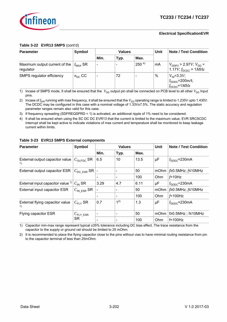
TC233 / TC234 / TC237
Electrical SpecificationEVR
Data Sheet 3-202 V 1.0 2017-03
Maximum output current of the regulator
IMAX SR - - 250 4) mA VDDP3 > 2.97V; VDD = 1.17V; fDCDC = 1MHz
SMPS regulator efficiency nDC CC - 72 - % VIN=3.3V; IDDDC=200mA; fDCDC=1MHz
1) Incase of SMPS mode, It shall be ensured that the VDD output pin shall be connected on PCB level to all other VDD Input pins.
2) Incase of fSRI running with max frequency, it shall be ensured that the VDD operating range is limited to 1.235V upto 1.430V. The DCDC may be configured in this case with a nominal voltage of 1.33V±7.5%. The static accuracy and regulation parameter ranges remain also valid for this case.
3) If frequency spreading (SDFREQSPRD = 1) is activated, an additional ripple of 1% need to be considered.4) It shall be ensured when using the SC DC DC EVR13 that the current is limited to the maximum value. EVR SRCSCDC
Interrupt shall be kept active to indicate violations of max current and temperature shall be monitored to keep leakage current within limits.
Table 3-23 EVR13 SMPS External componentsParameter Symbol Values Unit Note / Test Condition
Min. Typ. Max.External output capacitor value 1)
1) Capacitor min-max range represent typical ±35% tolerance including DC bias effect. The trace resistance from the capacitor to the supply or ground rail should be limited to 25 mOhm.
COUTDC SR 6.5 10 13.5 µF IDDDC=230mA
External output capacitor ESR CDC_ESR SR - - 50 mOhm f≥0.5MHz; f≤10MHz- - 100 Ohm f=10Hz
External input capacitor value 1) CIN SR 3.29 4.7 6.11 µF IDDDC=230mAExternal input capacitor ESR CIN_ESR SR - - 50 mOhm f≥0.5MHz; f≤10MHz
- - 100 Ohm f=100HzExternal flying capacitor value 1)
CFLY SR 0.7 12)
2) It is recommended to place the flying capacitor close to the pins without vias to have minimal routing resistance from pin to the capacitor terminal of less than 25mOhm.
1.3 µF IDDDC=230mA
Flying capacitor ESR CFLY_ESR SR
- - 50 mOhm f≥0.5MHz ; f≤10MHz- - 100 Ohm f=100Hz
Table 3-22 EVR13 SMPS (cont’d)
Parameter Symbol Values Unit Note / Test ConditionMin. Typ. Max.
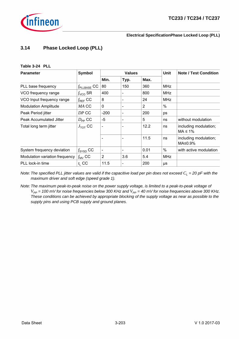
TC233 / TC234 / TC237
Electrical SpecificationPhase Locked Loop (PLL)
Data Sheet 3-203 V 1.0 2017-03
3.14 Phase Locked Loop (PLL)
Note: The specified PLL jitter values are valid if the capacitive load per pin does not exceed CL = 20 pF with the maximum driver and soft edge (speed grade 1).
Note: The maximum peak-to-peak noise on the power supply voltage, is limited to a peak-to-peak voltage of VPP = 100 mV for noise frequencies below 300 KHz and VPP = 40 mV for noise frequencies above 300 KHz.These conditions can be achieved by appropriate blocking of the supply voltage as near as possible to the supply pins and using PCB supply and ground planes.
Table 3-24 PLLParameter Symbol Values Unit Note / Test Condition
Min. Typ. Max.PLL base frequency fPLLBASE CC 80 150 360 MHzVCO frequency range fVCO SR 400 - 800 MHzVCO Input frequency range fREF CC 8 - 24 MHzModulation Amplitude MA CC 0 - 2 %Peak Period jitter DP CC -200 - 200 psPeak Accumulated Jitter DPP CC -5 - 5 ns without modulationTotal long term jitter JTOT CC - - 12.2 ns including modulation;
MA ≤ 1%- - 11.5 ns including modulation;
MA≤0.9%System frequency deviation fSYSD CC - - 0.01 % with active modulationModulation variation frequency fMV CC 2 3.6 5.4 MHzPLL lock-in time tL CC 11.5 - 200 µs

TC233 / TC234 / TC237
Electrical SpecificationERAY Phase Locked Loop (ERAY_PLL)
Data Sheet 3-204 V 1.0 2017-03
3.15 ERAY Phase Locked Loop (ERAY_PLL)
Note: The specified PLL jitter values are valid if the capacitive load per pin does not exceed CL = 20 pF with the maximum driver and soft edge (speed grade 1).
Note: The maximum peak-to-peak noise on the power supply voltage, is limited to a peak-to-peak voltage of VPP = 100 mV for noise frequencies below 300 KHz and VPP = 40 mV for noise frequencies above 300 KHz.These conditions can be achieved by appropriate blocking of the supply voltage as near as possible to the supply pins and using PCB supply and ground planes.
Table 3-25 PLL_ERAYParameter Symbol Values Unit Note / Test Condition
Min. Typ. Max.PLL Base Frequency of the ERAY PLL
fPLLBASE_ERA
Y CC50 200 320 MHz
VCO frequency range of the ERAY PLL
fVCO_ERAY SR
400 - 480 MHz
VCO input frequency of the ERAY PLL
fREF SR 16 - 24 MHz
Accumulated_Jitter DP CC -0.5 - 0.5 nsAccumulated jitter at SYSCLK pin
DPP CC -0.8 - 0.8 ns
PLL lock-in time tL CC 5.6 - 200 µs

TC233 / TC234 / TC237
Electrical SpecificationAC Specifications
Data Sheet 3-205 V 1.0 2017-03
3.16 AC SpecificationsAll AC parameters are specified for the complette operating range defined in Chapter 3.4 unless otherwise notedin colum Note / test Condition.
Unless otherwise noted in the figures the timings are defined with the following guidelines:
Figure 3-5 Definition of rise / fall times
Figure 3-6 Time Reference Point Definition
10%
90%
10%
90%
VSS
VDDP3
tr
rise_fall
tf
timing_reference
VDDP3Timing
Reference Points
VDDP3
VSS
VDDP3
2 2

TC233 / TC234 / TC237
Electrical SpecificationJTAG Parameters
Data Sheet 3-206 V 1.0 2017-03
3.17 JTAG ParametersThe following parameters are applicable for communication through the JTAG debug interface. The JTAG moduleis fully compliant with IEEE1149.1-2000.
Figure 3-7 Test Clock Timing (TCK)
Table 3-26 JTAGParameter Symbol Values Unit Note / Test Condition
Min. Typ. Max.TCK clock period t1 SR 25 - - nsTCK high time t2 SR 10 - - nsTCK low time t3 SR 10 - - nsTCK clock rise time t4 SR - - 4 nsTCK clock fall time t5 SR - - 4 nsTDI/TMS setup to TCK rising edge
t6 SR 6.0 - - ns
TDI/TMS hold after TCK rising edge
t7 SR 6.0 - - ns
TDO valid after TCK falling edge (propagation delay) 1)
1) The falling edge on TCK is used to generate the TDO timing.
t8 CC 3.0 - - ns CL≤20pF- - 16 ns CL≤50pF
TDO hold after TCK falling edge 1)
t18 CC 2 - - ns
TDO high impedance to valid from TCK falling edge 1)2)
2) The setup time for TDO is given implicitly by the TCK cycle time.
t9 CC - - 14 ns CL≤50pF
TDO valid output to high impedance from TCK falling edge 1)
t10 CC - - 13.5 ns CL≤50pF
MC_JTAG_TCK
0.9 VDDP0.5 VDDP
t1
t2 t3
0.1 VDDPt5 t4

TC233 / TC234 / TC237
Electrical SpecificationJTAG Parameters
Data Sheet 3-207 V 1.0 2017-03
Figure 3-8 JTAG Timing
t6 t7
t6 t7
t9 t8 t10
TCK
TMS
TDI
TDO
MC_JTAGt18

TC233 / TC234 / TC237
Electrical SpecificationDAP Parameters
Data Sheet 3-208 V 1.0 2017-03
3.18 DAP ParametersThe following parameters are applicable for communication through the DAP debug interface.
Figure 3-9 Test Clock Timing (DAP0)
Figure 3-10 DAP Timing Host to Device
Table 3-27 DAPParameter Symbol Values Unit Note / Test Condition
Min. Typ. Max.DAP0 clock period t11 SR 6.25 - - nsDAP0 high time t12 SR 2 - - nsDAP0 low time t13 SR 2 - - nsDAP0 clock rise time t14 SR - - 1 ns f=160MHz
- - 2 ns f=80MHzDAP0 clock fall time t15 SR - - 1 ns f=160MHz
- - 2 ns f=80MHzDAP1 setup to DAP0 rising edge
t16 SR 4 - - ns
DAP1 hold after DAP0 rising edge
t17 SR 2 - - ns
DAP1 valid per DAP0 clock period 1)
1) The Host has to find a suitable sampling point by analyzing the sync telegram response.
t19 CC 3 - - ns CL=20pF; f=160MHz8 - - ns CL=20pF; f=80MHz10 - - ns CL=50pF; f=40MHz
MC_DAP0
0.9 VDDP0.5 VDDP
t11
t12 t13
0.1 VDDPt15 t14
t16 t17
DAP0
DAP1
MC_DAP1_RX

TC233 / TC234 / TC237
Electrical SpecificationDAP Parameters
Data Sheet 3-209 V 1.0 2017-03
Figure 3-11 DAP Timing Device to Host (DAP1 and DAP2 pins)
Note: The DAP1 and DAP2 device to host timing is individual for both pins. There is no guaranteed max. signal skew.
DAP1
MC_DAP1_TX
t11
t19

TC233 / TC234 / TC237
Electrical SpecificationASCLIN SPI Master Timing
Data Sheet 3-210 V 1.0 2017-03
3.19 ASCLIN SPI Master TimingThis section defines the timings for the ASCLIN in the TC233 / TC234 / TC237.
Table 3-28 Master Mode A1+strong soft (sf) output padsParameter Symbol Values Unit Note / Test Condition
Min. Typ. Max.ASCLKO clock period 1)
1) PLL Jitter not included. Should be considered additionally, corresponding to the used baudrate. The duty cycle can be adjusted using the BITCON.SAMPLEPOINT bitfield with the finest granularity of TMAX = 1 / fMAX.
t50 CC 20 - - ns CL=25pFDeviation from ideal duty cycle 2)
2) Positive deviation lenghtens the high time and shortens the low time of a clock period. Negative deviation does the opposite.
t500 CC -3 - 3 ns CL=25pF
MTSR delay from ASCLKO shifting edge
t51 CC -4 - 4 ns CL=25pF
ASLSOn delay from the first ASCLKO edge
t510 CC -4 - 4 ns CL=25pF
MRST setup to ASCLKO latching edge
t52 SR 20 - - ns CL=25pF
MRST hold from ASCLKO latching edge
t53 SR -3 - - ns CL=25pF
Table 3-29 Master Mode A1+strong slow (sw) output padsParameter Symbol Values Unit Note / Test Condition
Min. Typ. Max.ASCLKO clock period 1)
1) PLL Jitter not included. Should be considered additionally, corresponding to the used baudrate. The duty cycle can be adjusted using the BITCON.SAMPLEPOINT bitfield with the finest granularity of TMAX = 1 / fMAX.
t50 CC 80 - - ns CL=50pFDeviation from ideal duty cycle 2)
2) Positive deviation lenghtens the high time and shortens the low time of a clock period. Negative deviation does the opposite.
t500 CC -8 - 8 ns CL=50pF
MTSR delay from ASCLKO shifting edge
t51 CC -12 - 12 ns CL=50pF
ASLSOn delay from the first ASCLKO edge
t510 CC -12 - 12 ns CL=50pF
MRST setup to ASCLKO latching edge
t52 SR 40 - - ns CL=50pF
MRST hold from ASCLKO latching edge
t53 SR -3 - - ns CL=50pF

TC233 / TC234 / TC237
Electrical SpecificationASCLIN SPI Master Timing
Data Sheet 3-211 V 1.0 2017-03
Table 3-30 Master Mode medium output padsParameter Symbol Values Unit Note / Test Condition
Min. Typ. Max.ASCLKO clock period 1)
1) PLL Jitter not included. Should be considered additionally, corresponding to the used baudrate. The duty cycle can be adjusted using the BITCON.SAMPLEPOINT bitfield with the finest granularity of TMAX = 1 / fMAX.
t50 CC 100 - - ns CL=50pFDeviation from ideal duty cycle 2)
2) Positive deviation lenghtens the high time and shortens the low time of a clock period. Negative deviation does the opposite.
t500 CC -10 - 10 ns CL=50pF
MTSR delay from ASCLKO shifting edge
t51 CC -15 - 15 ns CL=50pF
ASLSOn delay from the first ASCLKO edge
t510 CC -15 - 15 ns CL=50pF
MRST setup to ASCLKO latching edge
t52 SR 50 - - ns CL=50pF
MRST hold from ASCLKO latching edge
t53 SR -5 - - ns CL=50pF
Table 3-31 Master Mode weak output padsParameter Symbol Values Unit Note / Test Condition
Min. Typ. Max.ASCLKO clock period 1)
1) PLL Jitter not included. Should be considered additionally, corresponding to the used baudrate. The duty cycle can be adjusted using the BITCON.SAMPLEPOINT bitfield with the finest granularity of TMAX = 1 / fMAX.
t50 CC 1000 - - ns CL=50pFDeviation from ideal duty cycle 2)
2) Positive deviation lenghtens the high time and shortens the low time of a clock period. Negative deviation does the opposite.
t500 CC -25 - 25 ns CL=50pF
MTSR delay from ASCLKO shifting edge
t51 CC -65 - 65 ns CL=50pF
ASLSOn delay from the first ASCLKO edge
t510 CC -65 - 65 ns CL=50pF
MRST setup to ASCLKO latching edge
t52 SR 150 - - ns CL=50pF
MRST hold from ASCLKO latching edge
t53 SR -10 - - ns CL=50pF

TC233 / TC234 / TC237
Electrical SpecificationQSPI Timings, Master and Slave Mode
Data Sheet 3-212 V 1.0 2017-03
Figure 3-12 ASCLIN SPI Master Timing
3.20 QSPI Timings, Master and Slave ModeThis section defines the timings for the QSPI in the TC233 / TC234 / TC237. It is assumed that SCLKO, MTSR, and SLSO pads have the same pad settings:
Table 3-32 Master Mode timing A1+ strong soft (sf) output padsParameter Symbol Values Unit Note / Test Condition
Min. Typ. Max.SCLKO clock period 1)
1) Documented value is valid for master transmit or slave receive only. For full duplex the external SPI counterpart timing has to be taken into account.
t50 CC 20 - - ns CL=25pFDeviation from the ideal duty cycle 2) 3)
2) The PLL jitter is not included. It should be considered additionally, corresponding to the used baudrate. The duty cycle can be adjusted using the bit fields ECONz.A, B and C with the finest granularity of TMAX = 1 / fMAX.
3) Positive deviation lenghtens the high time and shortens the low time of a clock period. Negative deviation does the opposite.
t500 CC -3 - 3 ns CL=25pF
MTSR delay from SCLKO shifting edge
t51 CC -4 - 4 ns CL=25pF
SLSOn deviation from the ideal programmed position
t510 CC -4 - 4 ns CL=25pF
MRST setup to SCLK latching edge 4)
4) For compensation of the average on-chip delay the QSPI module provides the bit fields ECONz.A, B and C.
t52 SR 20 4) - - ns CL=25pF
MRST hold from SCLK latching edge
t53 SR -3 4) - - ns CL=25pF
ASCLIN_TmgMM.vsd
ASCLKO
MTSR
t51 t51
MRST
t53
Data valid
ASLSO
t510
t50
t500
t52
Data valid

TC233 / TC234 / TC237
Electrical SpecificationQSPI Timings, Master and Slave Mode
Data Sheet 3-213 V 1.0 2017-03
Table 3-33 Master Mode timing A1+ strong slow (sw) output padsParameter Symbol Values Unit Note / Test Condition
Min. Typ. Max.SCLKO clock period 1)
1) Documented value is valid for master transmit or slave receive only. For full duplex the external SPI counterpart timing has to be taken into account.
t50 CC 80 - - ns CL=50pFDeviation from the ideal duty cycle 2) 3)
2) The PLL jitter is not included. It should be considered additionally, corresponding to the used baudrate. The duty cycle can be adjusted using the bit fields ECONz.A, B and C with the finest granularity of TMAX = 1 / fMAX.
3) Positive deviation lenghtens the high time and shortens the low time of a clock period. Negative deviation does the opposite.
t500 CC -8 - 8 ns CL=50pF
MTSR delay from SCLKO shifting edge
t51 CC -12 - 12 ns CL=50pF
SLSOn deviation from the ideal programmed position
t510 CC -12 - 12 ns CL=50pF
MRST setup to SCLK latching edge 4)
4) For compensation of the average on-chip delay the QSPI module provides the bit fields ECONz.A, B and C.
t52 SR 40 4) - - ns CL=50pF
MRST hold from SCLK latching edge
t53 SR -3 - - ns CL=50pF
Table 3-34 Master Mode timing A1+m/A1m output padsParameter Symbol Values Unit Note / Test Condition
Min. Typ. Max.SCLKO clock period 1)
1) Documented value is valid for master transmit or slave receive only. For full duplex the external SPI counterpart timing has to be taken into account.
t50 CC 100 - - ns CL=50pFDeviation from the ideal duty cycle 2) 3)
2) The PLL jitter is not included. It should be considered additionally, corresponding to the used baudrate. The duty cycle can be adjusted using the bit fields ECONz.A, B and C with the finest granularity of TMAX = 1 / fMAX.
3) Positive deviation lenghtens the high time and shortens the low time of a clock period. Negative deviation does the opposite.
t500 CC -3 - 3 ns CL=50pF
MTSR delay from SCLKO shifting edge
t51 CC -8 - 8 ns CL=50pF
SLSOn deviation from the ideal programmed position
t510 CC -15 - 15 ns CL=50pF
MRST setup to SCLK latching edge 4)
4) For compensation of the average on-chip delay the QSPI module provides the bit fields ECONz.A, B and C.
t52 SR 50 4) - - ns CL=50pF
MRST hold from SCLK latching edge
t53 SR -5 4) - - ns CL=50pF

TC233 / TC234 / TC237
Electrical SpecificationQSPI Timings, Master and Slave Mode
Data Sheet 3-214 V 1.0 2017-03
Table 3-35 Master Mode Weak output padsParameter Symbol Values Unit Note / Test Condition
Min. Typ. Max.SCLKO clock period 1)
1) Documented value is valid for master transmit or slave receive only. For full duplex the external SPI counterpart timing has to be taken into account.
t50 CC 1000 - - ns CL=50pFDeviation from the ideal duty cycle 2) 3)
2) The PLL jitter is not included. It should be considered additionally, corresponding to the used baudrate. The duty cycle can be adjusted using the bit fields ECONz.A, B and C with the finest granularity of TMAX = 1 / fMAX.
3) Positive deviation lenghtens the high time and shortens the low time of a clock period. Negative deviation does the opposite.
t500 CC -25 - 25 ns CL=50pF
MTSR delay from SCLKO shifting edge
t51 CC -65 - 65 ns CL=50pF
SLSOn deviation from the ideal programmed position
t510 CC -65 - 65 ns CL=50pF
MRST setup to SCLK latching edge 4)
4) For compensation of the average on-chip delay the QSPI module provides the bit fields ECONz.A, B and C.
t52 SR 150 4) - - ns CL=50pF
MRST hold from SCLK latching edge
t53 SR -10 4) - - ns CL=50pF
Table 3-36 Slave mode timingParameter Symbol Values Unit Note / Test Condition
Min. Typ. Max.SCLK clock period t54 SR 4 x TMAX - - nsSCLK duty cycle t55/t54 SR 40 - 60 %MTSR setup to SCLK latching edge
t56 SR 3 - - ns
MTSR hold from SCLK latching edge
t57 SR 3 - - ns
SLSI setup to first SCLK shift edge
t58 SR 3 - - ns
SLSI hold from last SCLK latching edge
t59 SR 3 - - ns
MRST delay from SCLK shift edge
t60 CC 5 - 50 ns A1+m/A1m; CL=50pF3 - 20 ns A1+sf; CL=25pF5 - 40 ns A1+sw; CL=50pF10 - 150 ns A1+w/A1w; CL=50pF
SLSI to valid data on MRST t61 SR - - 9 ns

TC233 / TC234 / TC237
Electrical SpecificationQSPI Timings, Master and Slave Mode
Data Sheet 3-215 V 1.0 2017-03
Figure 3-13 Master Mode Timing
Figure 3-14 Slave Mode Timing
QSPI_TmgMM_EP.vsd
SCLK1)2)
MTSR1)
t51
MRST1)
t53
Data valid
SLSOn2)
1) This timing is based on the following setup : ECON.CPH = 1, ECON.CPOL = 0, ECON.B=0 (no sampling point delay ).
2) t510 is the deviation from the ideal position configured with the leading delay , BACON.LPRE and BACON.LEAD > 0.
t50
t500
t52
Data valid
SAMPLING POINT
t510
0.5 VDD3
0.5 VDD3
0.5 VDD3
QSPI_TmgSM_EP.vsd
SCLKI1)
t55
MTSR1)
t57
Datavalid
t56
SLSI
1) This timing is based on the following setup : ECON.CPH = 1, ECON.CPOL = 0.
t54
t55
t59
Last latching SCLK edge
First latching SCLK edge
t57
Datavalid
t56
MRST1)
t60
First shift SCLK edge
t60
t61
t58
0.5 VDD3
0.5 VDD3

TC233 / TC234 / TC237
Electrical SpecificationEthernet Interface (ETH) Characteristics
Data Sheet 3-216 V 1.0 2017-03
3.21 Ethernet Interface (ETH) Characteristics
3.21.1 ETH Measurement Reference Points
Figure 3-15 ETH Measurement Reference Points
ETH_Testpoints.vsd
ETH Clock 1.4 V 1.4 V
2.0 V0.8 V
2.0 V0.8 V
tR tF
ETH I/O

TC233 / TC234 / TC237
Electrical SpecificationEthernet Interface (ETH) Characteristics
Data Sheet 3-217 V 1.0 2017-03
3.21.2 ETH Management Signal Parameters (ETH_MDC, ETH_MDIO)
Figure 3-16 ETH Management Signal Timing
Table 3-37 ETH Management Signal ParametersParameter Symbol Values Unit Note / Test Condition
Min. Typ. Max.ETH_MDC period t1 CC 400 - - ns CL=25pFETH_MDC high time t2 CC 160 - - ns CL=25pFETH_MDC low time t3 CC 160 - - ns CL=25pFETH_MDIO setup time (output) t4 CC 10 - - ns CL=25pFETH_MDIO hold time (output) t5 CC 10 - - ns CL=25pFETH_MDIO data valid (input) t6 SR 0 - 300 ns CL=25pF
ETH_Timing-Mgmt.vsd
ETH_MDC
ETH_MDIO(output )
t5
Valid Data
t4
Valid Data
t6
ETH_MDIO(input )
ETH_MDC
ETH_MDIO sourced by controller :
ETH_MDIO sourced by PHY:
ETH_MDC
t1
t3 t2
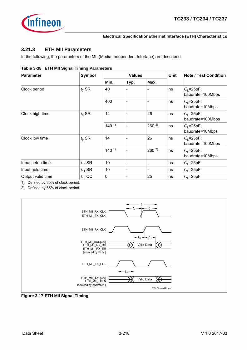
TC233 / TC234 / TC237
Electrical SpecificationEthernet Interface (ETH) Characteristics
Data Sheet 3-218 V 1.0 2017-03
3.21.3 ETH MII ParametersIn the following, the parameters of the MII (Media Independent Interface) are described.
Figure 3-17 ETH MII Signal Timing
Table 3-38 ETH MII Signal Timing ParametersParameter Symbol Values Unit Note / Test Condition
Min. Typ. Max.Clock period t7 SR 40 - - ns CL=25pF;
baudrate=100Mbps400 - - ns CL=25pF;
baudrate=10MbpsClock high time t8 SR 14 - 26 ns CL=25pF;
baudrate=100Mbps140 1)
1) Defined by 35% of clock period.
- 260 2)
2) Defined by 65% of clock period.
ns CL=25pF; baudrate=10Mbps
Clock low time t9 SR 14 - 26 ns CL=25pF; baudrate=100Mbps
140 1) - 260 2) ns CL=25pF; baudrate=10Mbps
Input setup time t10 SR 10 - - ns CL=25pFInput hold time t11 SR 10 - - ns CL=25pFOutput valid time t12 CC 0 - 25 ns CL=25pF
ETH_Timing-MII.vsd
ETH_MII_RX_CLK
ETH_MII_TXD[3:0]ETH_MII_TXEN
ETH_MII_RXD[3:0]ETH_MII_RX_DVETH_MII_RX_ER
ETH_MII_TX_CLK
t11
Valid Data
t10
Valid Data
t12
(sourced by controller )
(sourced by PHY)
t7
t9 t8ETH_MII_RX_CLKETH_MII_TX_CLK

TC233 / TC234 / TC237
Electrical SpecificationEthernet Interface (ETH) Characteristics
Data Sheet 3-219 V 1.0 2017-03
3.21.4 ETH RMII ParametersIn the following, the parameters of the RMII (Reduced Media Independent Interface) are described.
Figure 3-18 ETH RMII Signal Timing
Table 3-39 ETH RMII Signal Timing ParametersParameter Symbol Values Unit Note / Test Condition
Min. Typ. Max.ETH_RMII_REF_CL clock period
t13 CC 20 - - ns CL=25pF; 50ppm
ETH_RMII_REF_CL clock high time
t14 CC 7 1)
1) Defined by 35% of clock period.
- 13 2)
2) Defined by 65% of clock period.
ns CL=25pF
ETH_RMII_REF_CL clock low time
t15 CC 7 1) - 13 2) ns CL=25pF
ETHTXEN, ETHTXD[1:0], ETHRXD[1:0], ETHCRSDV, ETHRXER; setup time
t16 CC 4 - - ns CL=25pF
ETHTXEN, ETHTXD[1:0], ETHRXD[1:0], ETHCRSDV, ETHRXER; hold time
t17 CC 2 - - ns CL=25pF
ETH_Timing-RMII .vsd
ETH_RMII_REF_CL
t17
Valid Data
t16
t13
t15 t14
ETH_RMII_REF_CL
ETHTXEN, ETHTXD[1:0], ETHRXD[1:0],
ETHCRSDV, ETHRXER

TC233 / TC234 / TC237
Electrical SpecificationE-Ray Parameters
Data Sheet 3-220 V 1.0 2017-03
3.22 E-Ray ParametersThe timings of this section are valid for the strong driver and sharp edge settings of the output drivers with CL =25 pF.
Table 3-40 Transmit ParametersParameter Symbol Values Unit Note / Test Condition
Min. Typ. Max.Rise time of TxEN tdCCTxENRise2
5 CC- - 9 ns CL=25pF
Fall time of TxEN tdCCTxENFall25 CC
- - 9 ns CL=25pF
Sum of rise and fall time tdCCTxRise25+
dCCTxFall25 CC
- - 9 ns 20% - 80%; CL=25pF
Sum of delay between TP1_FF and TP1_CC and delays derived from TP1_FFi, rising edge of TxEN
tdCCTxEN01 CC
- - 25 ns
Sum of delay between TP1_FF and TP1_CC and delays derived from TP1_FFi, falling edge of TxEN
tdCCTxEN10 CC
- - 25 ns
Asymmetry of sending ttx_asym CC -2.45 - 2.45 ns CL=25pFSum of delay between TP1_FF and TP1_CC and delays derived from TP1_FFi, rising edge of TxD
tdCCTxD01 CC
- - 25 ns
Sum of delay between TP1_FF and TP1_CC and delays derived from TP1_FFi, falling edge of TxD
tdCCTxD10 CC
- - 25 ns
TxD signal sum of rise and fall time at TP1_BD
ttxd_sum CC - - 9 ns
Table 3-41 Receive ParametersParameter Symbol Values Unit Note / Test Condition
Min. Typ. Max.Acceptance of asymmetry at receiving part
tdCCTxAsymAcc
ept25 SR-30.5 - 43.0 ns CL=25pF
Acceptance of asymmetry at receiving part
tdCCTxAsymAcc
ept15 SR-31.5 - 44.0 ns CL=15pF
Threshold for detecting logical high
TuCCLogic1 SR
35 - 70 %
Threshold for detecting logical low
TuCCLogic0 SR
30 - 65 %

TC233 / TC234 / TC237
Electrical SpecificationE-Ray Parameters
Data Sheet 3-221 V 1.0 2017-03
Sum of delay between TP4_CC and TP4_FF and delays derived from TP4_FFi, rising edge of RxD
tdCCRxD01 CC
- - 10 ns
Sum of delay between TP1_CC and TP1_CC and delays derived from TP4_FFi, falling edge of RxD
tdCCRxD10 CC
- - 10 ns
Table 3-41 Receive Parameters (cont’d)
Parameter Symbol Values Unit Note / Test ConditionMin. Typ. Max.

TC233 / TC234 / TC237
Electrical SpecificationFlash Parameters
Data Sheet 3-222 V 1.0 2017-03
3.23 Flash ParametersProgram Flash program and erase operation is only allowed up the TJ = 150°C.
Table 3-42 FlashParameter Symbol Values Unit Note / Test Condition
Min. Typ. Max.Program Flash Erase Time per logical sector
tERP CC - - 1 s cycle count < 1000- 0.207 +
0.003 * (S [KByte]) / (fFSI [MHz])1)
- s cycle count < 1000, for sector of size S
Program Flash Erase Time per Multi-Sector Command
tMERP CC - - 1 s For consecutive logical sectors in a physical sector, cycle count < 1000
- 0.207 + 0.003 * (S [KByte]) / (fFSI [MHz])1)
- s For consecutive logical sector range of size S in a physical sector, cycle count < 1000
Program Flash program time per page in 3.3 V mode
tPRP3 CC - - 81 + 3400/(fFSI [MHz])
µs 32 Byte
Program Flash program time per burst in 3.3 V mode
tPRPB3 CC - - 410 + 12000/(fF
SI [MHz])
µs 256 Byte
Program Flash program time for 1 MByte with burst programming in 3 V mode excluding communication
tPRPB3_1MB CC
- - 2.2 s Derived value for documentation purpose, valid for fFSI = 100MHz
Write Page Once adder tADD CC - - 15 + 500/(fFSI [MHz])
µs Adder to Program Time when using Write Page Once
Program Flash suspend to read latency
tSPNDP CC - - 12000/(fF
SI [MHz]) µs For Write Burst, Verify
Erased and for multi-(logical) sector erase commands
Data Flash Erase Time per Sector 2)
tERD CC - 0.12 + 0.08/(fFSI [MHz])1)
- s cycle count < 1000
- 0.57 + 0.15/(fFSI [MHz])1)
0.928 + 0.15/(fFSI [MHz])
s cycle count < 125000
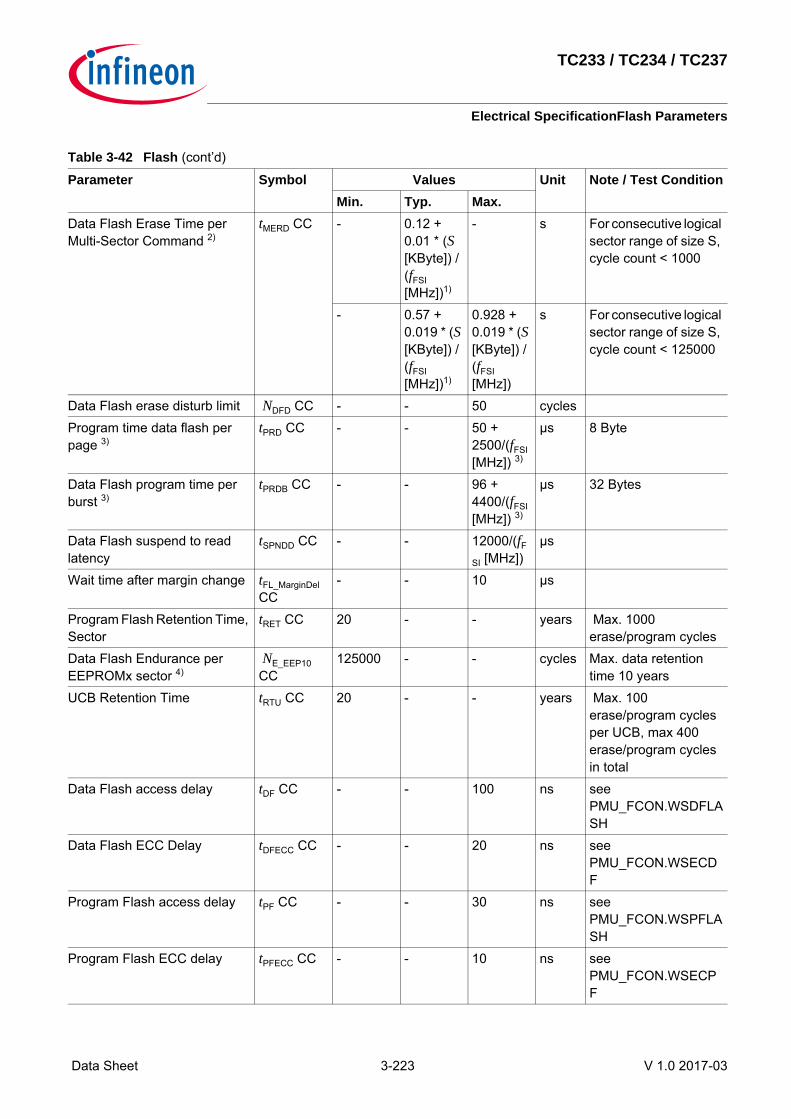
TC233 / TC234 / TC237
Electrical SpecificationFlash Parameters
Data Sheet 3-223 V 1.0 2017-03
Data Flash Erase Time per Multi-Sector Command 2)
tMERD CC - 0.12 + 0.01 * (S [KByte]) / (fFSI [MHz])1)
- s For consecutive logical sector range of size S, cycle count < 1000
- 0.57 + 0.019 * (S [KByte]) / (fFSI [MHz])1)
0.928 + 0.019 * (S [KByte]) / (fFSI [MHz])
s For consecutive logical sector range of size S, cycle count < 125000
Data Flash erase disturb limit NDFD CC - - 50 cyclesProgram time data flash per page 3)
tPRD CC - - 50 + 2500/(fFSI [MHz]) 3)
µs 8 Byte
Data Flash program time per burst 3)
tPRDB CC - - 96 + 4400/(fFSI [MHz]) 3)
µs 32 Bytes
Data Flash suspend to read latency
tSPNDD CC - - 12000/(fF
SI [MHz]) µs
Wait time after margin change tFL_MarginDel CC
- - 10 µs
Program Flash Retention Time, Sector
tRET CC 20 - - years Max. 1000 erase/program cycles
Data Flash Endurance per EEPROMx sector 4)
NE_EEP10 CC
125000 - - cycles Max. data retention time 10 years
UCB Retention Time tRTU CC 20 - - years Max. 100 erase/program cycles per UCB, max 400 erase/program cycles in total
Data Flash access delay tDF CC - - 100 ns see PMU_FCON.WSDFLASH
Data Flash ECC Delay tDFECC CC - - 20 ns see PMU_FCON.WSECDF
Program Flash access delay tPF CC - - 30 ns see PMU_FCON.WSPFLASH
Program Flash ECC delay tPFECC CC - - 10 ns see PMU_FCON.WSECPF
Table 3-42 Flash (cont’d)
Parameter Symbol Values Unit Note / Test ConditionMin. Typ. Max.

TC233 / TC234 / TC237
Electrical SpecificationFlash Parameters
Data Sheet 3-224 V 1.0 2017-03
Number of erase operations on DF0 over lifetime
NERD0 CC - - 750000 cycles
Junction temperature limit for PFlash program/erase operations
TJPFlash SR - - 150 °C
1) All typical values were characterised, but are not tested. Typical values are safe median values at room temperature2) Under out-of-spec conditions (e.g. over-cycling) or in case of activation of WL oriented defects, the duration of erase
processes may be increased by up to 50%.3) Time is not dependent on program mode (5V or 3.3V).4) Only valid when a robust EEPROM emulation algorithm is used. For more details see the Users Manual.
Table 3-42 Flash (cont’d)
Parameter Symbol Values Unit Note / Test ConditionMin. Typ. Max.

TC233 / TC234 / TC237
Electrical SpecificationPackage Outline
Data Sheet 3-225 V 1.0 2017-03
3.24 Package Outline
Figure 3-19 Package Outlines PG-LFBGA-292-6
CODE
STANDOFF
ABCDEFGHJK12345678910
INDEX
MARKING(LASERED )INDEX MARKING
0.1 C
1112
LM
1314
P N
SEAT
ING
PLAN
E
0.8
18
15
1716
2019
RTUVWY
COPLANARITY
292x
0.15
0.08 M C0.15 M C A B
292x
C
AB
17±0
.1
17 ±0.1
0.33 MIN
1.7 MAX
0.5 ±0.05
19 x 0.8 = 15.2
0.8
19 x
0.8
= 15
.2

TC233 / TC234 / TC237
Electrical SpecificationPackage Outline
Data Sheet 3-226 V 1.0 2017-03
Figure 3-20 Package Outlines PG-TQFP-144-27
Note: It is recommended to use dimensions Ex and Ey for board layout considerations. Solder wetting between Ex / Ey and Ax / Ay and lead between Ex / Ey and Ax / Ay will not case any harm.
Table 3-43 Exposed Pad DimensionsEx; vaild for Feature Package L and LP (nominal EPad size) 5.7 mm ± 50 µmEy; vaild for Feature Package L and LP (nominal EPad size) 5.7 mm ± 50 µmAx; vaild for Feature Package L and LP (solder able EPad size) 4.9 mm ± 50 µmAy; vaild for Feature Package L and LP (solder able EPad size) 4.9 mm ± 50 µm
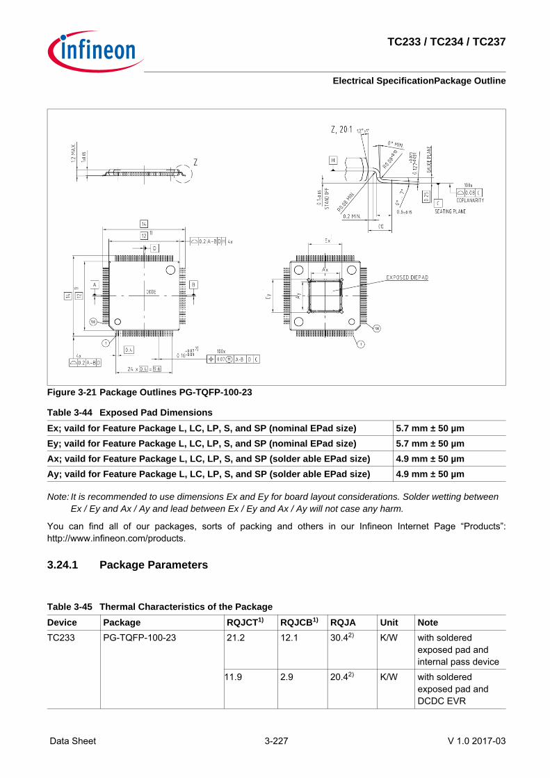
TC233 / TC234 / TC237
Electrical SpecificationPackage Outline
Data Sheet 3-227 V 1.0 2017-03
Figure 3-21 Package Outlines PG-TQFP-100-23
Note: It is recommended to use dimensions Ex and Ey for board layout considerations. Solder wetting between Ex / Ey and Ax / Ay and lead between Ex / Ey and Ax / Ay will not case any harm.
You can find all of our packages, sorts of packing and others in our Infineon Internet Page “Products”:http://www.infineon.com/products.
3.24.1 Package Parameters
Table 3-44 Exposed Pad DimensionsEx; vaild for Feature Package L, LC, LP, S, and SP (nominal EPad size) 5.7 mm ± 50 µmEy; vaild for Feature Package L, LC, LP, S, and SP (nominal EPad size) 5.7 mm ± 50 µmAx; vaild for Feature Package L, LC, LP, S, and SP (solder able EPad size) 4.9 mm ± 50 µmAy; vaild for Feature Package L, LC, LP, S, and SP (solder able EPad size) 4.9 mm ± 50 µm
Table 3-45 Thermal Characteristics of the PackageDevice Package RQJCT1) RQJCB1) RQJA Unit NoteTC233 PG-TQFP-100-23 21.2 12.1 30.42) K/W with soldered
exposed pad and internal pass device
11.9 2.9 20.42) K/W with soldered exposed pad and DCDC EVR

TC233 / TC234 / TC237
Electrical SpecificationPackage Outline
Data Sheet 3-228 V 1.0 2017-03
TC234 PG-TQFP-144-27 20.9 11.7 30.02) K/W with soldered exposed pad and internal pass device
11.7 2.8 19.82) K/W with soldered exposed pad and DCDC EVR
TC237 PG-LFBGA-292-6 13.7 21.0 33.12) K/W with internal pass device
7.6 14.1 25.42) K/W with DCDC EVR1) The top and bottom thermal resistances between the case and the ambient (RTCAT, RTCAB) are to be combined with the
thermal resistances between the junction and the case given above (RTJCT, RTJCB), in order to calculate the total thermal resistance between the junction and the ambient (RTJA). The thermal resistances between the case and the ambient (RTCAT, RTCAB) depend on the external system (PCB, case) characteristics, and are under user responsibility.The junction temperature can be calculated using the following equation: TJ = TA + RTJA * PD, where the RTJA is the total thermal resistance between the junction and the ambient. This total junction ambient resistance RTJA can be obtained from the upper four partial thermal resistances.Thermal resistances as measured by the ’cold plate method’ (MIL SPEC-883 Method 1012.1).
2) Value is defined in accordance with JEDEC JESD51-3, JESD51-5, and JESD51-7.
Table 3-45 Thermal Characteristics of the PackageDevice Package RQJCT1) RQJCB1) RQJA Unit Note

TC233 / TC234 / TC237
Electrical SpecificationQuality Declarations
Data Sheet 3-229 V 1.0 2017-03
3.25 Quality Declarations
Table 3-46 Quality ParametersParameter Symbol Values Unit Note / Test Condition
Min. Typ. Max.Operation Lifetime tOP - - 24500 hourESD susceptibility according to Human Body Model (HBM)
VHBM - - 2000 V Conforming to JESD22-A114-B
ESD susceptibility according to Charged Device Model (CDM)
VCDM - - 500 V for all other balls/pins; conforming to JESD22-C101-C
- - 750 V for corner balls/pins; conforming to JESD22-C101-C
Moisture Sensitivity Level MSL - - 3 Conforming to Jedec J-STD--020C for 240C

TC233 / TC234 / TC237
HistoryChanges from Version TC23x_DS_v1.1 to Version TC23xAC_DS_v1.0
Data Sheet 4-231 V 1.0 2017-03
4 History
4.1 Changes from Version TC23x_DS_v1.1 to Version TC23xAC_DS_v1.0This Data Sheet is only valid for the Feature Packages L, LC, LP, S, and SP.Feature Packages S and SP are newly added.
• PG-LFBGA-292-6 Package Varinat Pin Configuration of TC237x– Remove pin U17 from the NC list
• Overload– Remove parameter IING
• changes in table’ Class_S’ of Standard_Pads– add footenote ‘ VILx = 0.65 * VDDM’ to VIHS
– add footenote ‘ VILx = 0.41 * VDDM’ to VILS
• Back-up Clock– Add parameter fBACKSS
• EVR– Update footnote of EVR to 'It is recommended to place the flying capacitor close to the pins without vias to
have minimal routing resistance from pin to the capacitor terminal of less than 25mOhm. Likewise it is recommended to limit the routing resistance to input and output capacitor is to less than 25mOhm.'
• EVR/LDO– Update footnote of LDO to 'LDO operation is only possible for TJ≤150°C.'
• Changes in table 'VOUTT TC23xAC' of EVR/LDO– Change of VOUTT13 from load equal to IDD of max power pattern; either TJ≤150°C and pass device=on chip
or TJ≤170°C and pass device=off chip to load equal to IDD of max power pattern; pass device=on chip • VADC
– Add parameter tWU – Add parameter RMDU
– Add parameter RMDD • VADC_33
– Add parameter tWU – Add parameter RMDU
– Add parameter RMDD • Power Supply
– Change max value of IEVRSB from 650 µA to 150 µA – Change note of IEVRSB from 'Standby RAM is active. Power to remaining domains switched off. TJ =25°C'
to 'Standby RAM is active. Power to remaining domains switched off. TJ = 25°C; VEVRSB = 5V' – Change max value of IDDPORST from 70 mA to 85 mA for Note ‘valid for Feature Package L, LC, and LP;
TJ=165°C’– Change max value of IDDPORST from 45 mA to 60 mA for Note ‘valid for Feature Package L, LC, and LP;
TJ=150°C’

TC233 / TC234 / TC237
HistoryChanges from Version TC23x_DS_v1.1 to Version TC23xAC_DS_v1.0
Data Sheet 4-232 V 1.0 2017-03
– Change max value of IDDPORST from 25 mA to 40 mA for Note ‘valid for Feature Package L, LC, and LP; TJ=125°C’
– Update formulas 3.2 and 3.3– add formulas 3.4 and 3.5