301 EV BOARD USER GUIDE D L CC ZT · 60UG064E Rev.001 19 Feb 2018 Contents . 1 Board information...
18
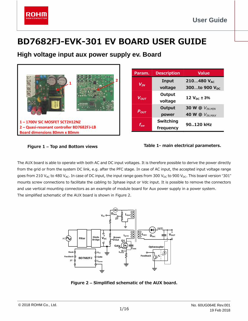
1/16 User Guide © 2018 ROHM Co., Ltd. No. 60UG064E Rev.001 19 Feb 2018 BD7682FJ-EVK-301 EV BOARD USER GUIDE High voltage input aux power supply ev. Board Figure 1 – Top and Bottom views The AUX board is able to operate with both AC and DC input voltages. It is therefore possible to derive the power directly from the grid or from the system DC link, e.g. after the PFC stage. In case of AC input, the accepted input voltage range goes from 210 V AC to 480 V AC . In case of DC input, the input range goes from 300 V DC to 900 V DC . This board version “301” mounts screw connections to facilitate the cabling to 3phase input or Vdc input. It is possible to remove the connectors and use vertical mounting connectors as an example of module board for Aux power supply in a power system. The simplified schematic of the AUX board is shown in Figure 2. Figure 2 – Simplified schematic of the AUX board. 1 – 1700V SiC MOSFET SCT2H12NZ 2 – Quasi-resonant controller BD7F682FJ-LB Board dimensions 80mm x 80mm 1 2 Dsec VOUT AC Filter Diode Bridge Lprim Lsec Laux Brown Out Gate VCC VCC Gate Isense ZT Feedback Isense Feedback BD7682FJ Q1 Daux COSS + - Optocoupler VDC + - ZT Mask Param. Description Value V IN Input voltage 210…480 V AC 300…to 900 V DC V OUT Output voltage 12 V DC ± 3% P OUT Output power 30 W @ V IN.MIN 40 W @ V IN.MAX f sw Switching frequency 90..120 kHz Table 1- main electrical parameters.
Transcript of 301 EV BOARD USER GUIDE D L CC ZT · 60UG064E Rev.001 19 Feb 2018 Contents . 1 Board information...
1/16
© 2017 ROHM Co., Ltd. No. 60AP001E Rev.001
2017.4
User Guide
© 2018 ROHM Co., Ltd. No. 60UG064E Rev.001
19 Feb 2018
BD7682FJ-EVK-301 EV BOARD USER GUIDE
High voltage input aux power supply ev. Board
Figure 1 – Top and Bottom views
The AUX board is able to operate with both AC and DC input voltages. It is therefore possible to derive the power directly
from the grid or from the system DC link, e.g. after the PFC stage. In case of AC input, the accepted input voltage range
goes from 210 VAC to 480 VAC. In case of DC input, the input range goes from 300 VDC to 900 VDC. This board version “301”
mounts screw connections to facilitate the cabling to 3phase input or Vdc input. It is possible to remove the connectors
and use vertical mounting connectors as an example of module board for Aux power supply in a power system.
The simplified schematic of the AUX board is shown in Figure 2.
Figure 2 – Simplified schematic of the AUX board.
1 – 1700V SiC MOSFET SCT2H12NZ 2 – Quasi-resonant controller BD7F682FJ-LB Board dimensions 80mm x 80mm
1 2
DsecVOUT
AC FilterDiode Bridge
LprimLsec
Laux
Brown Out
Gate
VCC
VCC
Gate
IsenseZT
Feedback
Isense
FeedbackBD7682FJ
Q1
Daux
COSS
+
-
Optocoupler
VDC
+
-
ZT
Mask
Param. Description Value
VIN Input
voltage
210…480 VAC
300…to 900 VDC
VOUT Output
voltage 12 VDC ± 3%
POUT Output
power
30 W @ VIN.MIN
40 W @ VIN.MAX
fsw Switching
frequency 90..120 kHz
Table 1- main electrical parameters.
2/16
User Guide BD7682FJ-EVK-301 EV BOARD
© 2018 ROHM Co., Ltd.
No. 60TRxxxJ Rev.001
No. 60UG064E Rev.001
19 Feb 2018
Contents
1 Board information ....................................................................................................................................... 3
1.1 Schematics........................................................................................................................................ 3
1.2 Flyback Transformer ........................................................................................................................... 3
2 Board usage............................................................................................................................................... 4
2.1 General information before cabling and powering the board: ................................................................... 4
2.2 Cabling ............................................................................................................................................. 5
2.2.1 3 Phase AC connections: ............................................................................................................... 5
2.2.2 DC connections: ........................................................................................................................... 5
2.3 Test points ........................................................................................................................................ 6
3 Implementation and practical tests with AUX Board ........................................................................................ 7
3.1 Operation at no load ........................................................................................................................... 7
3.2 Normal operation ............................................................................................................................... 8
3.3 Efficiency and temperature measurements ............................................................................................ 8
4 Summary ................................................................................................................................................ 10
5 References ............................................................................................................................................... 10
Appendix A. Transformer datasheet and pictures ................................................................................... 11
Appendix B. Bill of Materials ............................................................................................................... 12
Appendix C. AUX Board layout ............................................................................................................ 14
Appendix D. Alternative Start-up Circuitry ............................................................................................ 15
This evaluation board is intended for research and development and for expert use in the research and
development facility only. This board is not intended for use for volume production.

3/16
User Guide BD7682FJ-EVK-301 EV BOARD
© 2018 ROHM Co., Ltd.
No. 60TRxxxJ Rev.001
No. 60UG064E Rev.001
19 Feb 2018
1 Board information
1.1 Schematics
Please refer to Appendix B for BOM, Appendix C for Layout and Appendix D for alternative startup circuit to improve
efficiency.
1.2 Flyback Transformer
A customized transformer manufactured by Würth Elektronik (www.we-online.com), has been designed.
It is possible to order and get all the information by contacting the producer referring code n. 750316318.
The datasheet of the transformer can be found in Appendix A.
The primary side is composed by two windings in series, while the secondary side has been implemented with two
windings in parallel. The half-windings are interposed, in order to reduce the leakage inductance around 1% of Lpri. This
will impact the switching behavior of the MOSFET. In addition, the windings have been implemented with Litz wire to
reduce the losses due to skin effect.
Parameter Calculated Transformer (E25)
Primary inductance 1.07 mH 0.95 mH ±10%
Leakage inductance -- 1% (9 µH)
Maximum primary current 0.86 A 1.5 A *
Turn-ratio primary to secondary 10 10 ± 1%
Turn-ratio secondary to auxiliary 1.92 2 ± 1%
Table 2 - Calculated parameters and characteristics of the used transformer.
Figure 3 - Full schematic of the AUX board
* Core saturation current
4/16
User Guide BD7682FJ-EVK-301 EV BOARD
© 2018 ROHM Co., Ltd.
No. 60TRxxxJ Rev.001
No. 60UG064E Rev.001
19 Feb 2018
2 Board usage
2.1 General information before cabling and powering the board:
- Check carefully that the input voltages are within the maximum input range in table 1.
- Double check the cabling before powering the board.
- This board is protected against overload and short circuit.
- Avoid any imperfect connection that can create sparks
- Check the isolation class and section of the cables.
- Apply all appropriate checks and precautions for use of a high voltage board.
- Refer to the notice at the end of this document for proper usage of this board.
- Only use in a technical environment by professionals trained to safely manage high voltage boards.
- This board is only for evaluation purposes and it’s not guaranteed for prolonged usage or usage
in any final product

5/16
User Guide BD7682FJ-EVK-301 EV BOARD
© 2018 ROHM Co., Ltd.
No. 60TRxxxJ Rev.001
No. 60UG064E Rev.001
19 Feb 2018
2.2 Cabling
2.2.1 3 Phase AC connections:
The board can be connected directly to 3 Phase mains as for the below connection guide.
Figure 4 - 3Phase AC connection
2.2.2 DC connections:
If the board is connected to an DC source please follow the below connection guide
Figure 5 – DC Voltage input connection
Please note that the board mounts diodes for the possibility to be supplied by AC. Due to high voltage input compatibility
are used 2 diodes in series. To avoid the drop of diodes effect on functionalities (i.e. efficiency measurements) connect
directly to the positive of Capacitor C6 and negative of capacitor C8
Phase 1
Phase 2
Phase 3
Neutral
12Vdc To Load +
Volt Ref To Load -
400Vac to
480Vac 3 Phase
Input DC Voltage+
Input DC Voltage -
12Vdc To Load +
Volt Ref To Load -
6/16
User Guide BD7682FJ-EVK-301 EV BOARD
© 2018 ROHM Co., Ltd.
No. 60TRxxxJ Rev.001
No. 60UG064E Rev.001
19 Feb 2018
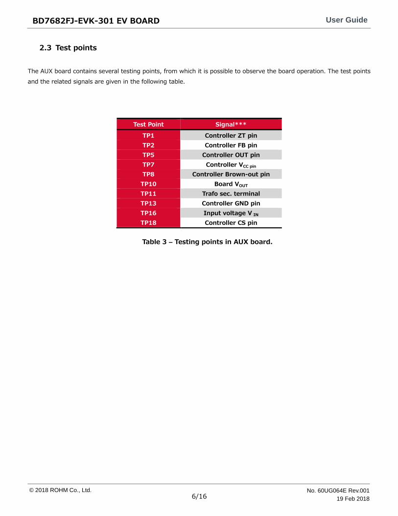
2.3 Test points
The AUX board contains several testing points, from which it is possible to observe the board operation. The test points
and the related signals are given in the following table.
Test Point Signal***
TP1 Controller ZT pin
TP2 Controller FB pin
TP5 Controller OUT pin
TP7 Controller VCC pin
TP8 Controller Brown-out pin
TP10 Board VOUT
TP11 Trafo sec. terminal
TP13 Controller GND pin
TP16 Input voltage V IN
TP18 Controller CS pin
Table 3 – Testing points in AUX board.

7/16
User Guide BD7682FJ-EVK-301 EV BOARD
© 2018 ROHM Co., Ltd.
No. 60TRxxxJ Rev.001
No. 60UG064E Rev.001
19 Feb 2018
3 Implementation and practical tests with AUX Board
The AUX board has been implemented in a printed circuit board (PCB), whose dimensions are 8 cm x 8 cm – see Figure
6. All surface mount devices (SMD) components have been assembled on the bottom side. On the top side were soldered
the thru hole devices (THD) and connectors. The layout of both sides is given in Appendix C. In the following sections,
experimental results at different input voltages and output power are presented and discussed.
Figure 6 – Top side (left) and bottom side (right) of the AUX board.
3.1 Operation at no load
At no load operation, the controller goes in burst mode – see Figure 16 – and the switching frequency is reduced to some
kHz. The dynamic losses of the Flyback components are consequently reduced. Measured stand-by losses are given in the
table on the right side of Figure 7. They are expected to come mainly from the resistive dividers present on the circuit:
input capacitor balance, start-up and input voltage sense.
DC voltage Stand-by losses
300 V 0.372 W
900 V 1.7 W
Figure 7 – Waveforms from Flyback switch during burst mode, for VDC = 800 V.
T1
Q1
D20
U1
VGS
VDS
VDC=800V

8/16
User Guide BD7682FJ-EVK-301 EV BOARD
© 2018 ROHM Co., Ltd.
No. 60TRxxxJ Rev.001
No. 60UG064E Rev.001
19 Feb 2018
3.2 Normal operation
Figure 8 presents the waveforms from SCT2H12NZ during normal operation of the Flyback circuit, for VDC = 800 V and
different values of output power. Time periods ton, tdecay and tdelay are indicated, according to the description in Error!
eference source not found..
For light power – left side – the controller waits several valleys to switch the MOSFET on. Therefore, the switching
frequency is quite low, eventually below the defined frequency range.
As the output power increases, the number of oscillations is reduced. As consequence, tdelay is reduced, and the switching
frequency increases. At nominal power, the turn-on occurs already in the first valley.
Pout= 5W
Pout= 20W
Pout= 40W
Figure 8 – Waveforms from Flyback switch during different output power conditions, VDC = 800 V.
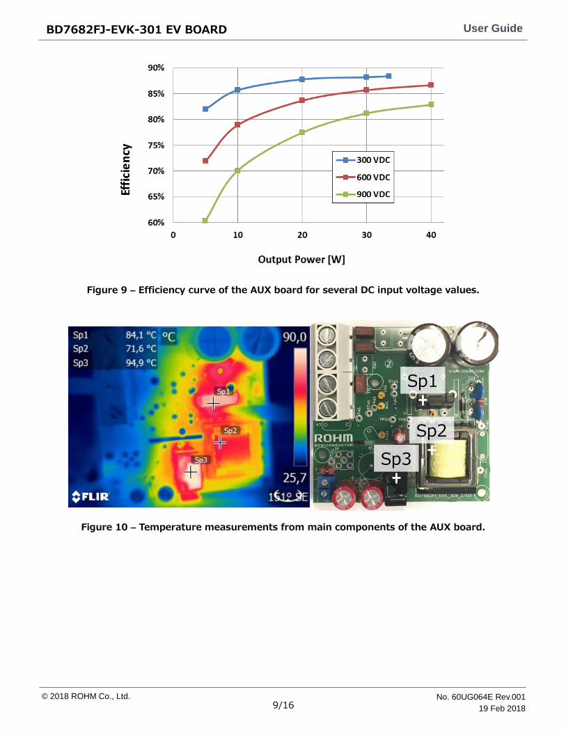
3.3 Efficiency and temperature measurements
The efficiency of the AUX board has been measured for three different input voltage values. The efficiency curves are
shown in Figure 9. As a DC power source was used, it was connected directly to the input capacitors. This way, the
rectifying bridge is by-passed, saving the losses that would otherwise come from the bridge diodes.
Efficiency is increasing with the output power, and it is higher for lower levels of input voltage. For VDC = 300 V, the
measured peak efficiency η=88% at POUT=33W – above that the overload protection was activated.
The temperature of the main components of AUX board has been measured, namely the SiC MOSFET (Q1), the Flyback
transformer and the secondary diode (D20). The measurements were performed using an infrared camera. The thermal
images are presented in Figure 10. They were taken at room temperature, VDC=800 V and POUT=40W. The case
temperature of the SiC MOSFET (Sp1) is around 84°C, even without the use of an external heatsink and without forced
ventilation. The temperature of the Flyback transformer (Sp2), registered on the winding corner, is slightly above 70°C.
The measured temperature of the output diode (Sp3) was around 95°C.
VGS
VDS
tdelaytdecay
ton
fsw=45.7 kHz
VDC=800 V
VGS
VDS
fsw=105.0 kHz
VDC=800 V
VGS
VDS
VDC=800 V
fsw=109.0 kHz
9/16
User Guide BD7682FJ-EVK-301 EV BOARD
© 2018 ROHM Co., Ltd.
No. 60TRxxxJ Rev.001
No. 60UG064E Rev.001
19 Feb 2018
Figure 9 – Efficiency curve of the AUX board for several DC input voltage values.
Figure 10 – Temperature measurements from main components of the AUX board.
Sp1
Sp2
Sp3

10/16
User Guide BD7682FJ-EVK-301 EV BOARD
© 2018 ROHM Co., Ltd.
No. 60TRxxxJ Rev.001
No. 60UG064E Rev.001
19 Feb 2018
4 Summary
This document presented the design procedure of an auxiliary power supply, based on Flyback topology, focused on
industrial applications as auxiliary power supply. Main devices of this design are the SiC MOSFET SCT2H12NZ, with very
low on resistance, and the quasi resonant controller BDF768xFJ-LB. They enable a simple electrical and thermal design,
reducing the amount of devices, and avoiding the use of heat-sink for the Flyback switch.
Experimental tests in the AUX board proved the operation principle of the quasi resonant controller. Thermal and efficient
measurements showed also the reduced amount of losses in the SiC MOSFET, proving it is the right choice for auxiliary
supplies in 3-phase industrial systems.
5 References
[1] Datasheet of SCT2H12NZ http://www.rohm.com/web/global/datasheet/SCT2H12NZ/sct2h12nz-e
[2] Datasheet of BDF768xFJ-LB controller family, available at:
http://www.rohm.de/web/de/products/-/product/BD7682FJ-LB
[3] Application Note “BD768xFJ-LB series Quasi-Resonant converter Technical Design”, available at:
http://rohmfs.rohm.com/en/products/databook/applinote/ic/power/acdc_converter/bd768xfj-lb_appli-e.pdf

11/16
User Guide BD7682FJ-EVK-301 EV BOARD
© 2018 ROHM Co., Ltd.
No. 60TRxxxJ Rev.001
No. 60UG064E Rev.001
19 Feb 2018
Appendix A. Transformer datasheet and pictures
Fig. A.1 – Datasheet of the constructed Flyback transformer.
Fig. A.2 – Side view (left) and top view (right) of the Flyback transformer.
12/16
User Guide BD7682FJ-EVK-301 EV BOARD
© 2018 ROHM Co., Ltd.
No. 60TRxxxJ Rev.001
No. 60UG064E Rev.001
19 Feb 2018
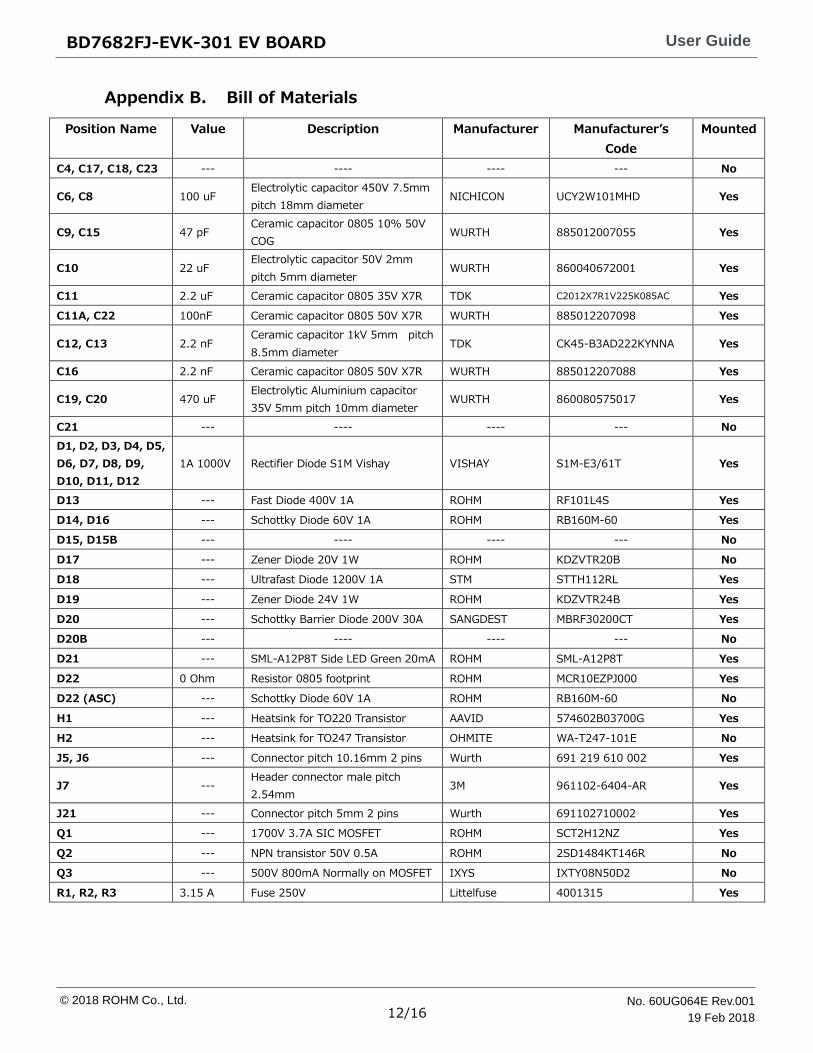
Appendix B. Bill of Materials
Position Name Value Description Manufacturer Manufacturer’s
Code
Mounted
C4, C17, C18, C23 --- ---- ---- --- No
C6, C8 100 uF Electrolytic capacitor 450V 7.5mm
pitch 18mm diameter NICHICON UCY2W101MHD Yes
C9, C15 47 pF Ceramic capacitor 0805 10% 50V
COG WURTH 885012007055 Yes
C10 22 uF Electrolytic capacitor 50V 2mm
pitch 5mm diameter WURTH 860040672001 Yes
C11 2.2 uF Ceramic capacitor 0805 35V X7R TDK C2012X7R1V225K085AC Yes
C11A, C22 100nF Ceramic capacitor 0805 50V X7R WURTH 885012207098 Yes
C12, C13 2.2 nF Ceramic capacitor 1kV 5mm pitch
8.5mm diameter TDK CK45-B3AD222KYNNA Yes
C16 2.2 nF Ceramic capacitor 0805 50V X7R WURTH 885012207088 Yes
C19, C20 470 uF Electrolytic Aluminium capacitor
35V 5mm pitch 10mm diameter WURTH 860080575017 Yes
C21 --- ---- ---- --- No
D1, D2, D3, D4, D5,
D6, D7, D8, D9,
D10, D11, D12
1A 1000V Rectifier Diode S1M Vishay VISHAY S1M-E3/61T Yes
D13 --- Fast Diode 400V 1A ROHM RF101L4S Yes
D14, D16 --- Schottky Diode 60V 1A ROHM RB160M-60 Yes
D15, D15B --- ---- ---- --- No
D17 --- Zener Diode 20V 1W ROHM KDZVTR20B No
D18 --- Ultrafast Diode 1200V 1A STM STTH112RL Yes
D19 --- Zener Diode 24V 1W ROHM KDZVTR24B Yes
D20 --- Schottky Barrier Diode 200V 30A SANGDEST MBRF30200CT Yes
D20B --- ---- ---- --- No
D21 --- SML-A12P8T Side LED Green 20mA ROHM SML-A12P8T Yes
D22 0 Ohm Resistor 0805 footprint ROHM MCR10EZPJ000 Yes
D22 (ASC) --- Schottky Diode 60V 1A ROHM RB160M-60 No
H1 --- Heatsink for TO220 Transistor AAVID 574602B03700G Yes
H2 --- Heatsink for TO247 Transistor OHMITE WA-T247-101E No
J5, J6 --- Connector pitch 10.16mm 2 pins Wurth 691 219 610 002 Yes
J7 --- Header connector male pitch
2.54mm 3M 961102-6404-AR Yes
J21 --- Connector pitch 5mm 2 pins Wurth 691102710002 Yes
Q1 --- 1700V 3.7A SIC MOSFET ROHM SCT2H12NZ Yes
Q2 --- NPN transistor 50V 0.5A ROHM 2SD1484KT146R No
Q3 --- 500V 800mA Normally on MOSFET IXYS IXTY08N50D2 No
R1, R2, R3 3.15 A Fuse 250V Littelfuse 4001315 Yes

13/16
User Guide BD7682FJ-EVK-301 EV BOARD
© 2018 ROHM Co., Ltd.
No. 60TRxxxJ Rev.001
No. 60UG064E Rev.001
19 Feb 2018
Position Name Value Description Manufacturer Manufacturer’s
Code
Mounted
R4, R4B, R6, R6B,
R7, R8, R9, R10 470kOhm Resistor 1206 footprint ROHM MCR18ERTF4703 Yes
R11 10kOhm Resistor 0805 footprint ROHM MCR10ERTF1002 Yes
R12A, R13A, R14A,
R35, R39 0 Ohm Resistor 0805 footprint ROHM MCR10EZPJ000 No
R16 4.7kOhm Resistor 0805 footprint ROHM MCR10ERTF4701 Yes
R17 330kOhm Resistor 2W V VISHAY PR02000203303JR500 Yes
R18 100 Ohm Resistor 0805 footprint ROHM MCR10ERTF1000 Yes
R19 10 Ohm Resistor 0805 footprint ROHM MCR10ERTF10R0 Yes
R20 47kOhm Resistor 0805 footprint ROHM MCR10ERTF4702 Yes
R21, R21A 3 Ohm Resistor footprint 1020 Wide ROHM LTR50UZPF3R00 Yes
R21B 6.8 Ohm Resistor footprint 1020 Wide ROHM LTR50UZPF6R80 Yes
R22, R38 0 Ohm Resistor 0805 footprint ROHM MCR10EZPJ000 Yes
R23 120kOhm Resistor 0805 footprint ROHM MCR10ERTF1203 Yes
R24, R30 12kOhm Resistor 0805 footprint ROHM MCR10ERTF1202 Yes
R25 300 Ohm Resistor 0805 footprint ROHM MCR10ERTF3000 Yes
R26, R37 1kOhm Resistor 0805 footprint ROHM MCR10ERTF1001 Yes
R27 15kOhm Resistor 0805 footprint ROHM MCR10ERTF1502 Yes
R28 180kOhm Resistor 0805 footprint ROHM MCR10ERTF1803 Yes
R29 51kOhm Resistor 0805 footprint ROHM MCR10ERTF5102 Yes
R31 --- ---- ---- --- No
R34 4.7kOhm Resistor 0805 footprint ROHM MCR10ERTF4701 No
R36 10kOhm Res 0805 footprint ROHM MCR10ERTF1002 No
T1 --- FLyback Transformer WURTH 750316318 Yes
U1 --- ACDC flyback driver for SIC
MOSFET ROHM BD7682 Yes
U2 --- 5kV Optocoupler SHARP PC817XNNIP0F Yes
U3 --- Voltage reference 2.49V TI TL431AIDBZR Yes

14/16
User Guide BD7682FJ-EVK-301 EV BOARD
© 2018 ROHM Co., Ltd.
No. 60TRxxxJ Rev.001
No. 60UG064E Rev.001
19 Feb 2018
Appendix C. AUX Board layout
Fig. C.1 – Layout of top side (left) and bottom side (right) of the AUX board.
15/16
User Guide BD7682FJ-EVK-301 EV BOARD
© 2018 ROHM Co., Ltd.
No. 60TRxxxJ Rev.001
No. 60UG064E Rev.001
19 Feb 2018
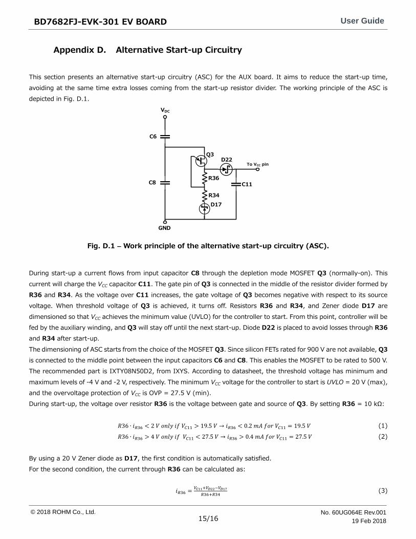
Appendix D. Alternative Start-up Circuitry
This section presents an alternative start-up circuitry (ASC) for the AUX board. It aims to reduce the start-up time,
avoiding at the same time extra losses coming from the start-up resistor divider. The working principle of the ASC is
depicted in Fig. D.1.
Fig. D.1 – Work principle of the alternative start-up circuitry (ASC).
During start-up a current flows from input capacitor C8 through the depletion mode MOSFET Q3 (normally-on). This
current will charge the VCC capacitor C11. The gate pin of Q3 is connected in the middle of the resistor divider formed by
R36 and R34. As the voltage over C11 increases, the gate voltage of Q3 becomes negative with respect to its source
voltage. When threshold voltage of Q3 is achieved, it turns off. Resistors R36 and R34, and Zener diode D17 are
dimensioned so that VCC achieves the minimum value (UVLO) for the controller to start. From this point, controller will be
fed by the auxiliary winding, and Q3 will stay off until the next start-up. Diode D22 is placed to avoid losses through R36
and R34 after start-up.
The dimensioning of ASC starts from the choice of the MOSFET Q3. Since silicon FETs rated for 900 V are not available, Q3
is connected to the middle point between the input capacitors C6 and C8. This enables the MOSFET to be rated to 500 V.
The recommended part is IXTY08N50D2, from IXYS. According to datasheet, the threshold voltage has minimum and
maximum levels of -4 V and -2 V, respectively. The minimum VCC voltage for the controller to start is UVLO = 20 V (max),
and the overvoltage protection of VCC is OVP = 27.5 V (min).
During start-up, the voltage over resistor R36 is the voltage between gate and source of Q3. By setting R36 = 10 kΩ:
𝑅36 ∙ 𝑖𝑅36 < 2 𝑉 𝑜𝑛𝑙𝑦 𝑖𝑓 𝑉𝐶11 > 19.5 𝑉 → 𝑖𝑅36 < 0.2 𝑚𝐴 𝑓𝑜𝑟 𝑉𝐶11 = 19.5 𝑉 (1)
𝑅36 ∙ 𝑖𝑅36 > 4 𝑉 𝑜𝑛𝑙𝑦 𝑖𝑓 𝑉𝐶11 < 27.5 𝑉 → 𝑖𝑅36 > 0.4 𝑚𝐴 𝑓𝑜𝑟 𝑉𝐶11 = 27.5 𝑉 (2)
By using a 20 V Zener diode as D17, the first condition is automatically satisfied.
For the second condition, the current through R36 can be calculated as:
𝑖𝑅36 =𝑉𝐶11+𝑉𝐷22−𝑉𝐷17
𝑅36+𝑅34 (3)
VDC
GND
To VCC pin
C6
C8 C11R36
D22Q3
D17
R34

16/16
User Guide BD7682FJ-EVK-301 EV BOARD
© 2018 ROHM Co., Ltd.
No. 60TRxxxJ Rev.001
No. 60UG064E Rev.001
19 Feb 2018
Which leads to:
𝑅34 <27.5 𝑉+0.3 𝑉−20𝑉
0.4 𝑚𝐴− 10 𝑘Ω → 𝑅34 < 9.5 𝑘Ω (4)
Chosen value for R34 = 4.7 kΩ.
Fig. D.2 presents the waveforms of the start-up of the AUX board, done by standard configuration and with ASC. It is
possible to observe that the start-up time is reduced by a factor of 100. Moreover, since the start-up resistive divider is not
used in ASC, the losses caused by those resistors are not present in the ASC configuration
Fig. D.2 – Schematics of the AUX board with alternative start-up circuitry (ASC).
The full schematic of AUX board with implemented ASC is depicted in Fig. D.3. Devices different from original schematics
are drawn in a different color. Please note they are not assembled in the original board. However, their respective
footprints are present on the board, assuming the devices given in the bill of materials list – see Appendix B.
In addition to extra components, the resistors R38 and R12 must be removed. Finally, before D22 is placed, the originally
soldered 0 Ω resistor must be removed.
Fig. D.3 – Schematics of the AUX board with alternative start-up circuitry (ASC).
Q1 VDS
VCC
UVLO
~100 ms
Standard start-up
VCC
<1 ms Q3 VDS
Q3 VGS
UVLO
Standard through ASC
6
Notice
ROHM Customer Support System http://www.rohm.com/contact/
Thank you for your accessing to ROHM product informations. More detail product informations and catalogs are available, please contact us.
N o t e s
The information contained herein is subject to change without notice.
Before you use our Products, please contact our sales representative and verify the latest specifica-tions :
Although ROHM is continuously working to improve product reliability and quality, semicon-ductors can break down and malfunction due to various factors.Therefore, in order to prevent personal injury or fire arising from failure, please take safety measures such as complying with the derating characteristics, implementing redundant and fire prevention designs, and utilizing backups and fail-safe procedures. ROHM shall have no responsibility for any damages arising out of the use of our Poducts beyond the rating specified by ROHM.
Examples of application circuits, circuit constants and any other information contained herein are provided only to illustrate the standard usage and operations of the Products. The peripheral conditions must be taken into account when designing circuits for mass production.
The technical information specified herein is intended only to show the typical functions of and examples of application circuits for the Products. ROHM does not grant you, explicitly or implicitly, any license to use or exercise intellectual property or other rights held by ROHM or any other parties. ROHM shall have no responsibility whatsoever for any dispute arising out of the use of such technical information.
The Products specified in this document are not designed to be radiation tolerant.
For use of our Products in applications requiring a high degree of reliability (as exemplified below), please contact and consult with a ROHM representative : transportation equipment (i.e. cars, ships, trains), primary communication equipment, traffic lights, fire/crime prevention, safety equipment, medical systems, servers, solar cells, and power transmission systems.
Do not use our Products in applications requiring extremely high reliability, such as aerospace equipment, nuclear power control systems, and submarine repeaters.
ROHM shall have no responsibility for any damages or injury arising from non-compliance with the recommended usage conditions and specifications contained herein.
ROHM has used reasonable care to ensur the accuracy of the information contained in this document. However, ROHM does not warrants that such information is error-free, and ROHM shall have no responsibility for any damages arising from any inaccuracy or misprint of such information.
Please use the Products in accordance with any applicable environmental laws and regulations, such as the RoHS Directive. For more details, including RoHS compatibility, please contact a ROHM sales office. ROHM shall have no responsibility for any damages or losses resulting non-compliance with any applicable laws or regulations.
When providing our Products and technologies contained in this document to other countries, you must abide by the procedures and provisions stipulated in all applicable export laws and regulations, including without limitation the US Export Administration Regulations and the Foreign Exchange and Foreign Trade Act.
This document, in part or in whole, may not be reprinted or reproduced without prior consent of ROHM.
1)
2)
3)
4)
5)
6)
7)
8)
9)
10)
11)
12)
13)

<High Voltage Safety Precautions>
Read all safety precautions before use Please note that this document covers only the BD7682FJ & SCT2H12NZ evaluation board
(BD7682FJ-EVK-301) and its functions. For additional information, please refer to the datasheet.
To ensure safe operation, please carefully read all precautions before handling the evaluation board
Depending on the configuration of the board and voltages used,
Potentially lethal voltages may be generated. Therefore, please make sure to read and observe all safety precautions described in the red box below.
Before Use [1] Verify that the parts/components are not damaged or missing (i.e. due to the drops).[2] Check that there are no conductive foreign objects on the board. [3] Be careful when performing soldering on the module and/or evaluation board to ensure that
solder splash does not occur. [4] Check that there is no condensation or water droplets on the circuit board.
During Use
[5] Be careful to not allow conductive objects to come into contact with the board. [6] Brief accidental contact or even bringing your hand close to the board may result in
discharge and lead to severe injury or death.Therefore, DO NOT touch the board with your bare hands or bring them too close to the board. In addition, as mentioned above please exercise extreme caution when using conductive tools such as tweezers and screwdrivers.
[7] If used under conditions beyond its rated voltage, it may cause defects such as short-circuit or, depending on the circumstances, explosion or other permanent damages.
[8] Be sure to wear insulated gloves when handling is required during operation. After Use
[9] The ROHM Evaluation Board contains the circuits which store the high voltage. Since it stores the charges even after the connected power circuits are cut, please discharge the electricity after using it, and please deal with it after confirming such electric discharge.
[10] Protect against electric shocks by wearing insulated gloves when handling.
This evaluation board is intended for use only in research and development facilities and should by handled only by qualified personnel familiar with all safety and operating procedures.We recommend carrying out operation in a safe environment that includes the use of high voltage signage at all entrances, safety interlocks, and protective glasses.