300V and 375V Design Guide - Powel.ru
40
Design Guide DC-DC Converters 12 300V & 375V INPUT FAMILIES
Transcript of 300V and 375V Design Guide - Powel.ru
Design GuideDC-DC Converters
12
3 0 0 V & 3 7 5 VI N P U T F A M I L I E S
w w w . v i c o r p o w e r . c o m
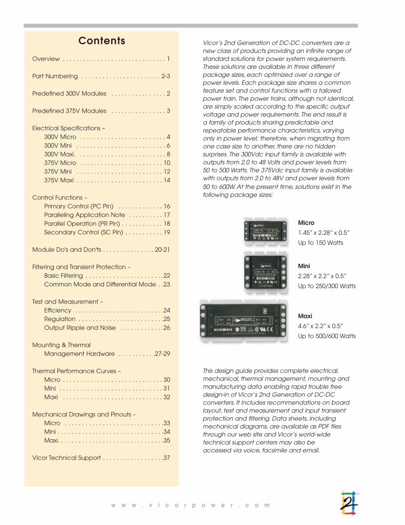
Vicor’s 2nd Generation of DC-DC converters are anew class of products providing an infinite range ofstandard solutions for power system requirements.These solutions are available in three differentpackage sizes, each optimized over a range ofpower levels. Each package size shares a commonfeature set and control functions with a tailoredpower train. The power trains, although not identical,are simply scaled according to the specific outputvoltage and power requirements. The end result isa family of products sharing predictable andrepeatable performance characteristics, varying only in power level; therefore, when migrating fromone case size to another, there are no hiddensurprises. The 300Vdc input family is available withoutputs from 2.0 to 48 Volts and power levels from50 to 500 Watts. The 375Vdc input family is availablewith outputs from 2.0 to 48V and power levels from 50 to 600W. At the present time, solutions exist in thefollowing package sizes:
Micro
1.45” x 2.28” x 0.5”
Up to 150 Watts
Mini
2.28” x 2.2” x 0.5”
Up to 250/300 Watts
Maxi
4.6” x 2.2” x 0.5”
Up to 500/600 Watts
This design guide provides complete electrical,mechanical, thermal management, mounting andmanufacturing data enabling rapid trouble freedesign-in of Vicor’s 2nd Generation of DC-DCconverters. It includes recommendations on boardlayout, test and measurement and input transientprotection and filtering. Data sheets, includingmechanical diagrams, are available as PDF filesthrough our web site and Vicor’s world-widetechnical support centers may also be accessed via voice, facsimile and email.
Overview . . . . . . . . . . . . . . . . . . . . . . . . . . . . . . 1
Part Numbering . . . . . . . . . . . . . . . . . . . . . . . 2-3
Predefined 300V Modules . . . . . . . . . . . . . . . . 2
Predefined 375V Modules . . . . . . . . . . . . . . . . 3
Electrical Specifications –300V Micro . . . . . . . . . . . . . . . . . . . . . . . . . 4300V Mini . . . . . . . . . . . . . . . . . . . . . . . . . . 6300V Maxi. . . . . . . . . . . . . . . . . . . . . . . . . . 8375V Micro . . . . . . . . . . . . . . . . . . . . . . . . 10375V Mini . . . . . . . . . . . . . . . . . . . . . . . . . 12375V Maxi . . . . . . . . . . . . . . . . . . . . . . . . . 14
Control Functions – Primary Control (PC Pin) . . . . . . . . . . . . . 16Paralleling Application Note . . . . . . . . . . 17Parallel Operation (PR Pin) . . . . . . . . . . . . 18Secondary Control (SC Pin) . . . . . . . . . . . 19
Module Do's and Don'ts . . . . . . . . . . . . . . . 20-21
Filtering and Transient Protection –Basic Filtering . . . . . . . . . . . . . . . . . . . . . . .22Common Mode and Differential Mode . .23
Test and Measurement –Efficiency . . . . . . . . . . . . . . . . . . . . . . . . . .24Regulation . . . . . . . . . . . . . . . . . . . . . . . . .25Output Ripple and Noise . . . . . . . . . . . . .26
Mounting & Thermal Management Hardware . . . . . . . . . . .27-29
Thermal Performance Curves –Micro . . . . . . . . . . . . . . . . . . . . . . . . . . . . . 30Mini . . . . . . . . . . . . . . . . . . . . . . . . . . . . . . 31Maxi . . . . . . . . . . . . . . . . . . . . . . . . . . . . . 32
Mechanical Drawings and Pinouts –Micro . . . . . . . . . . . . . . . . . . . . . . . . . . . . .33Mini . . . . . . . . . . . . . . . . . . . . . . . . . . . . . . .34Maxi. . . . . . . . . . . . . . . . . . . . . . . . . . . . . . .35
Vicor Technical Support . . . . . . . . . . . . . . . . . .37
Contents

v i c o r p o w e r . c o m 1
Autoranging90-132Vac/100-214Vac
Autoranging90-132Vac/100-214Vac
Autoranging115/230Vac/Input
Filter /Autoranging Rectifier Module
Up to 1000W
Up to 500W per module2-100Vdc
FARM
MINIHAM
300V MaxiDC-DC Converter
300V MINI
DC-DC Converter
Up to 250W per module2-48Vdc
DC-DC Converter
Up to 150W per module2-48Vdc
300VMICRO
4.6" x 2.2" x 0.5"(116,9 x 55,9 x 12,7 mm)
2.28" x 2.2" x 0.5"(57,9 x 55,9 x 12,7 mm)
2.28" x 1.45" x 0.5"(57,9 x 36,8 x 12,7 mm)
Up to 1500W
Autoranging Rectifier Module
Single Wire Paralleling for High Power, Fault Tolerant Arrays
300V Component Power SolutionsAC-DC Products DC-DC Products
ARM
Front End System for EN Comliance
Up to 1000W
Up to 600W per module2-100Vdc
375V MaxiDC-DC Converter
375V MINI
DC-DC Converter
Up to 300W per module2-48Vdc
DC-DC Converter
Up to 150W per module2-48Vdc
375VMICRO
4.6" x 2.2" x 0.5"(116,9 x 55,9 x 12,7 mm)
2.28" x 2.2" x 0.5"(57,9 x 55,9 x 12,7 mm)
2.28" x 1.45" x 0.5"(57,9 x 36,8 x 12,7 mm)
Vendor Dependent
Power Factor Correction Single Wire Paralleling for High Power, Fault Tolerant Arrays
375V Component Power SolutionsAC-DC Products DC-DC Products
85-214Vac
180-264Vac
Fixed OutputPFC
VI-HAM
Harmonic Attenuator ModuleUnity Power Factor
Up to 600Wper module
FARM4
Up to 550W

2 v i c o r p o w e r . c o m
Part Numbering300V Input Family of DC-DC Converters
V 300 A 15 C 500 A LInput Package Output Product Output Pin Style1 Baseplate1
Voltage Voltage Grade PowerA = Maxi C = -20°C to 100°C blank=short solder blank=slottedB = Mini T = -40°C to 100°C L=long solder 2=threadedC = Micro H = -40°C to 100°C S=short ModuMate 3=thru-hole
M = -55°C to 100°C N=long ModuMate
Output Voltage (Vdc) Output Power (Watts) Vicor Model Number Package Size
2.0 50 V300C2C50A Micro
2.0 100 V300B2C100A Mini
2.0 160 V300A2C160A Maxi
3.3 75 V300C3V3C75A Micro
3.3 150 V300B3V3C150A Mini
3.3 264 V300A3V3C264A Maxi
5.0 100 V300C5C100A Micro
5.0 200 V300B5C200A Mini
5.0 400 V300A5C400A Maxi
12.0 150 V300C12C150A Micro
12.0 250 V300B12C250A Mini
12.0 500 V300A12C500A Maxi
15.0 150 V300C15C150A Micro
15.0 250 V300B15C250A Mini
15.0 500 V300A15C500A Maxi
24.0 150 V300C24C150A Micro
24.0 250 V300B24C250A Mini
24.0 500 V300A24C500A Maxi
28.0 150 V300C28C150A Micro
28.0 250 V300B28C250A Mini
28.0 500 V300A28C500A Maxi
48.0 150 V300C48C150A Micro
48.0 250 V300B48C250A Mini
48.0 500 V300A48C500A Maxi
1 See pages 33-35
Product Grades C T H M
Operating Temp. –20 to 100°C –40 to 100°C –40 to 100°C –55 to 100°CStorage Temp. –40 to 125°C –40 to 125°C –55 to 125°C –65 to 125°CTemp. Cycling N/A N/A 24 hours (–55 to 125°C) 24 hours (–65 to 125°C)Burn-In N/A N/A 12 hours 24 hoursLow Temp. Test N/A N/A –40°C –55°CHigh Temp. Test N/A N/A 100°C 100°CFinal Test Data N/A N/A Available Available
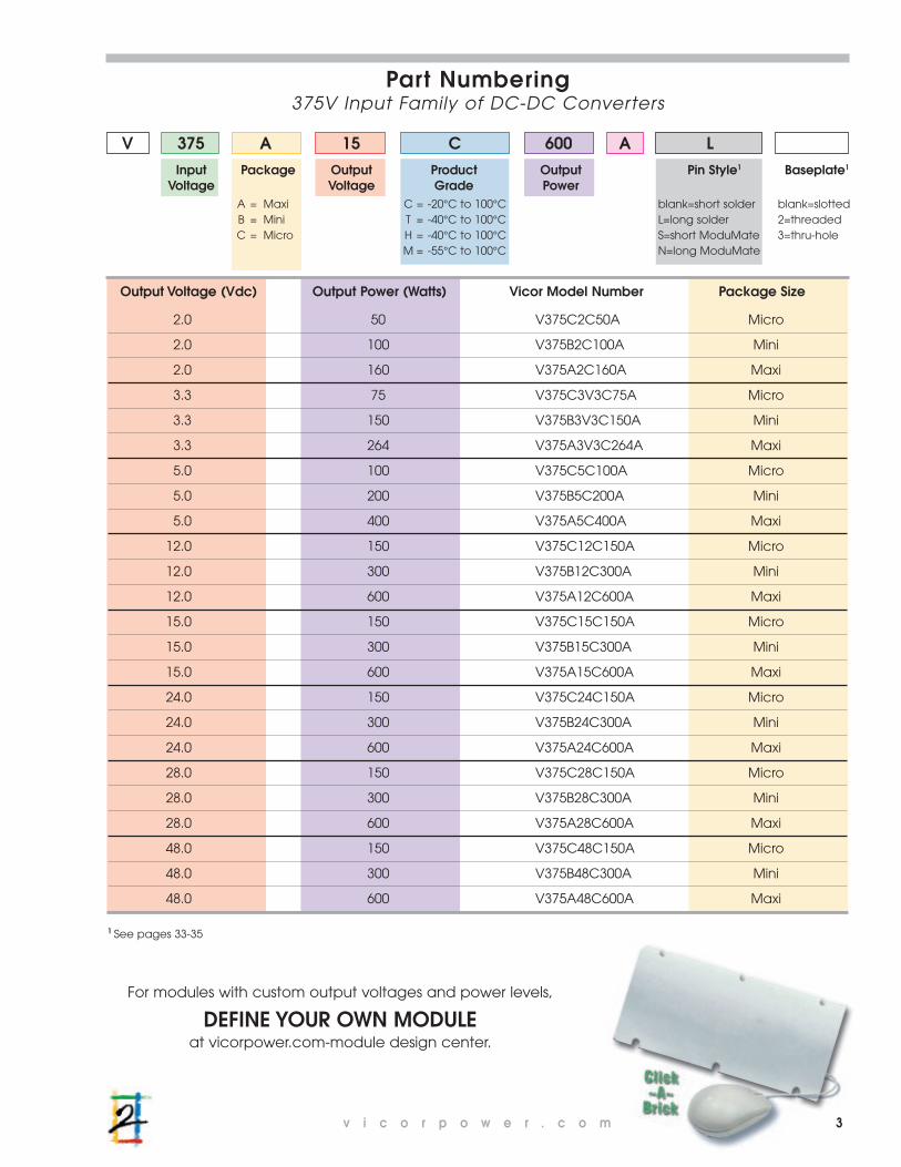
For modules with custom output voltages and power levels,
DEFINE YOUR OWN MODULE at vicorpower.com-module design center.
Part Numbering375V Input Family of DC-DC Converters
V 375 A 15 C 600 A LInput Package Output Product Output Pin Style1 Baseplate1
Voltage Voltage Grade PowerA = Maxi C = -20°C to 100°C blank=short solder blank=slottedB = Mini T = -40°C to 100°C L=long solder 2=threadedC = Micro H = -40°C to 100°C S=short ModuMate 3=thru-hole
M = -55°C to 100°C N=long ModuMate
Output Voltage (Vdc) Output Power (Watts) Vicor Model Number Package Size
2.0 50 V375C2C50A Micro
2.0 100 V375B2C100A Mini
2.0 160 V375A2C160A Maxi
3.3 75 V375C3V3C75A Micro
3.3 150 V375B3V3C150A Mini
3.3 264 V375A3V3C264A Maxi
5.0 100 V375C5C100A Micro
5.0 200 V375B5C200A Mini
5.0 400 V375A5C400A Maxi
12.0 150 V375C12C150A Micro
12.0 300 V375B12C300A Mini
12.0 600 V375A12C600A Maxi
15.0 150 V375C15C150A Micro
15.0 300 V375B15C300A Mini
15.0 600 V375A15C600A Maxi
24.0 150 V375C24C150A Micro
24.0 300 V375B24C300A Mini
24.0 600 V375A24C600A Maxi
28.0 150 V375C28C150A Micro
28.0 300 V375B28C300A Mini
28.0 600 V375A28C600A Maxi
48.0 150 V375C48C150A Micro
48.0 300 V375B48C300A Mini
48.0 600 V375A48C600A Maxi
v i c o r p o w e r . c o m 3
1 See pages 33-35

4 v i c o r p o w e r . c o m
Electrical Specifications300V MICRO
MODULE INPUT SPECIFICATIONSParameter Min Typ Max Unit Notes
Operating input voltage 180 300 375 Vdc
Undervoltage turn-on 174.6 178.2 Vdc
Undervoltage turn-off 147.4 152.8 Vdc
Overvoltage turn-off/on Vdc Not included
Input surge withstand 400 Vdc <100ms
MODULE CONTROL SPECIFICATIONSPrimary Side: PC = Primary Control • PR = Parallel
Parameter Min Typ Max Unit Notes
PC bias voltage 5.5 5.7 6.0 Vdc PC current = 1.0mA
PC current limit 1.5 2.1 3 mA PC voltage = 5.5V
PC module disable 2.3 2.6 2.9 Vdc Must be able to sink ≥4mA. See Figure 1, p. 16
PC module enable delay 4 7 ms
PC module alarm 0.5 Vavg UV OV, OT, module fault. See Figures 2, 4, p. 16
PR emitter amplitude 5.7 5.9 6.1 Volts PR load >30ohms, <30pF
PR emitter current 150 mA
PR receiver impedance 375 500 625 ohms 25°C
PR receiver threshold 2.4 2.5 2.6 Volts Minimum pulse width; 20ns
PR drive capability 12 modules >12 modules will require buffer amplifier
MODULE GENERAL SPECIFICATIONSParameter Min Typ Max Unit Notes
Remote sense (total drop) n/a
Isolation voltage (in to out) 3000 Vrms Complies with reinforced insulation requirements
Isolation voltage in to base) 1550 Vrms Complies with basic insulation requirements
Isolation voltage (out to base) 500 Vrms Complies with operational insulation requirements
Isolation resistance (in to out) 10 megohms
Weight 2.1(60) 2.3(66) ounces(grams)
Temperature limiting 100 115 °C See Figures 2, 4, p. 16
Agency approvals UL, CSA, TÜV, BABT, CE, VDE UL1950, CSA950, EN60950, VDE 0805, BS7002IEC60950, (with a fuse in series with the +Input)
Electrical characteristics apply over the full operating range of input voltage, output load (resistive) and baseplatetemperature, unless otherwise specified. All temperatures refer to the operating temperature at the center of the baseplate.

v i c o r p o w e r . c o m 5
Electrical Specifications300V MICRO
MODULE OUTPUT SPECIFICATIONSParameter Min Typ Max Unit Notes
Output voltage setpoint ±1% Vout nom Nom. input; full load, 25°C
Line regulation ±0.02 ±0.2 % Low line to high line; full load
Temperature regulation ±0.002 ±0.005 %/°C Over operating temp. range
Power sharing accuracy ±2 ±5 % 10% to 100% of full load
Programming range 10 110 % Of nominal output voltage.For trimming below 90% of nom.a minimum load of 10% of maximum rated power maybe required
Current limit 115 % Iout max. Output voltage 95% of nominal
Short circuit current 115 % Iout max. Output voltage <250mV
MODULE OUTPUT VOLTAGE RELATED SPECIFICATIONSParameter 1.8V1 2V 2.5V2 3.3V 5V 12V 15V 24V 28V 48V Unit Notes
Efficiency (typ.) 70.0 70.0 74.8 76.5 80.0 84.0 85.5 86.0 86.5 88.0 % Nom. input; 80%load, 25°C
Ripple & Noise, p-p (typ.) 120 120 120 120 105 170 150 150 180 55 mV Nom. input; full load; 25°C; 20MHz BW
Output power (max.) 45 50 57 75 100 150 150 150 150 150 Watts 100°C Baseplate
Output OVP setpoint 2.8 2.8 4.3 4.3 6.3 14.3 17.8 28.1 32.7 55.7 Volts 25°C; recycle input voltageto restart (1 min. off)
Dissipation, standby (typ.) 2.6 2.6 3.4 3.4 4.4 5.0 7.0 4.9 4.6 4.0 Watts No load; nom input
Load regulation (max.) 0.5 0.5 0.4 0.4 0.2 0.2 0.2 0.2 0.3 0.2 ±%Vout No Load to full load; nom. input
MODULE CONTROL SPECIFICATIONSSecondary Side: SC = Secondary Control
Parameter Min Typ Max Unit Notes
SC bandgap voltage 1.21 1.23 1.25 Vdc Referenced to -Out
SC resistance 990 1000 1010 ohms
SC capacitance 0.033 µF
SC module alarm 0 Vdc With open trim, referencedto -Out. See Figure 6, p. 16
1 Nominal 2V output trimmed to 1.8V by adding external 9,000 ohm resister from the SC pin to -Out pin. (See Figure 14, p. 19)
2 Nominal 3.3V output trimmed to 2.5V by adding external 3,125 ohm resister from the SC pin to -Out pin. (See Figure 14, p. 19)

6 v i c o r p o w e r . c o m
MODULE INPUT SPECIFICATIONSParameter Min Typ Max Unit Notes
Operating input voltage 180 300 375 Vdc
Undervoltage turn-on 174.6 178.2 Vdc
Undervoltage turn-off 147.4 152.8 Vdc
Overvoltage turn-off/on Vdc Not included
Input surge withstand 400 Vdc <100ms
MODULE CONTROL SPECIFICATIONSPrimary Side: PC = Primary Control • PR = Parallel
Parameter Min Typ Max Unit Notes
PC bias voltage 5.5 5.7 6.0 Vdc PC current = 1.0mA
PC current limit 1.5 2.1 3.0 mA PC voltage = 5.5V
PC module disable 2.3 2.6 2.9 Vdc Must be able to sink ≥4mA. See Figure 1, p. 16
PC module enable delay 4 7 ms
PC module alarm 0.5 Vavg UV, OV, OT, module fault. See Figures 2, 4, p. 16
PR emitter amplitude 5.7 5.9 6.1 Volts PR load >30ohms, <30pF
PR emitter current 150 mA
PR receiver impedance 375 500 625 ohms 25°C
PR receiver threshold 2.4 2.5 2.6 Volts Minimum pulse width; 20ns
PR drive capability 12 modules >12 modules will require buffer amplifier
MODULE GENERAL SPECIFICATIONSParameter Min Typ Max Unit Notes
Remote sense (total drop) 0.5 Vdc 0.25V/leg (sense leads must be closed)
Isolation voltage (in to out) 3000 Vrms Complies with reinforced insulation requirements
Isolation voltage in to base) 1550 Vrms Complies with basic insulation requirements
Isolation voltage (out to base) 500 Vrms Complies with operational insulation requirements
Isolation resistance (in to out) 10 megohms
Weight 3.7(104) 4(112) ounces(grams)
Temperature limiting 100 115 °C See Figures 2, 4, p. 16
Agency approvals UL, CSA, TÜV, BABT, CE, VDE UL1950, CSA950, EN60950, VDE 0805, BS7002IEC60950, (with a fuse in series with the +Input)
Electrical characteristics apply over the full operating range of input voltage, output load (resistive) and baseplatetemperature, unless otherwise specified. All temperatures refer to the operating temperature at the center of the baseplate.
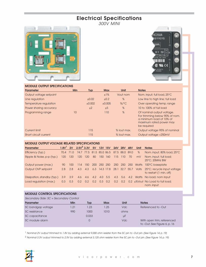
Electrical Specifications300V MINI
v i c o r p o w e r . c o m 7
MODULE OUTPUT SPECIFICATIONSParameter Min Typ Max Unit Notes
Output voltage setpoint ±1% Vout nom Nom. input; full load, 25°C
Line regulation ±0.02 ±0.2 % Low line to high line; full load
Temperature regulation ±0.002 ±0.005 %/°C Over operating temp. range
Power sharing accuracy ±2 ±5 % 10 to 100% of full load
Programming range 10 110 % Of nominal output voltage.For trimming below 90% of nom.a minimum load of 10% of maximum rated power may be required
Current limit 115 % Iout max. Output voltage 95% of nominal
Short circuit current 115 % Iout max. Output voltage <250mV
MODULE OUTPUT VOLTAGE RELATED SPECIFICATIONSParameter 1.8V1 2V 2.5V2 3.3V 5V 12V 15V 24V 28V 48V Unit Notes
Efficiency (typ.) 70.4 71.0 74.7 77.5 81.5 85.0 86.5 87.5 88.0 89.0 % Nom. input; 80% load, 25°C
Ripple & Noise, p-p (typ.) 120 120 120 120 80 150 160 115 110 70 mV Nom. input; full load;25°C; 20MHz BW
Output power (max.) 90 100 114 150 200 250 250 250 250 250 Watts 100°C baseplate
Output OVP setpoint 2.8 2.8 4.3 4.3 6.3 14.3 17.8 28.1 32.7 55.7 Volts 25°C; recycle input voltageto restart (1 min. off)
Dissipation, standby (typ.) 3.9 3.9 4.6 4.6 4.2 4.0 5.5 4.3 5.6 4.2 Watts No load; nom input
Load regulation (max.) 0.3 0.3 0.2 0.2 0.2 0.3 0.2 0.2 0.2 0.2 ±%Vout No Load to full load;nom. input
MODULE CONTROL SPECIFICATIONSSecondary Side: SC = Secondary Control
Parameter Min Typ Max Unit Notes
SC bandgap voltage 1.21 1.23 1.25 Vdc Referenced to -Out
SC resistance 990 1000 1010 ohms
SC capacitance 0.033 µF
SC module alarm 0 Vdc With open trim, referencedto -Out. See Figure 6, p. 16
1 Nominal 2V output trimmed to 1.8V by adding external 9,000 ohm resister from the SC pin to -Out pin. (See Figure 14, p. 19)
2 Nominal 3.3V output trimmed to 2.5V by adding external 3,125 ohm resister from the SC pin to -Out pin. (See Figure 14, p. 19)
Electrical Specifications300V MINI

8 v i c o r p o w e r . c o m
MODULE INPUT SPECIFICATIONSParameter Min Typ Max Unit Notes
Operating input voltage 180 300 375 Vdc
Undervoltage turn-on 174.6 178.2 Vdc
Undervoltage turn-off 147.4 152.8 Vdc
Overvoltage turn-off/on Vdc Not included
Input surge withstand 400 Vdc <100ms
MODULE CONTROL SPECIFICATIONSPrimary Side: PC = Primary Control • PR = Parallel
Parameter Min Typ Max Unit Notes
PC bias voltage 5.5 5.7 6.0 Vdc PC current = 1.0mA
PC current limit 1.5 2.1 3.0 mA PC voltage = 5.5V
PC module disable 2.3 2.6 2.9 Vdc Must be able to sink ≥4mA. See Figure 1, p. 8
PC module enable delay 4 7 ms
PC module alarm 0.5 Vavg UV, OV, OT, module fault. See Figures 2, 4, p. 8
PR emitter amplitude 5.7 5.9 6.1 Volts PR load >30ohms, <30pF
PR emitter current 150 mA
PR receiver impedance 375 500 625 ohms 25°C
PR receiver threshold 2.4 2.5 2.6 Volts Minimum pulse width; 20ns
PR drive capability 12 modules >12 modules will require buffer amplifier
MODULE GENERAL SPECIFICATIONSParameter Min Typ Max Unit Notes
Remote sense (total drop) 0.5 Vdc 0.25V/leg (sense leads must be closed)
Isolation voltage (in to out) 3000 Vrms Complies with reinforced insulation requirements
Isolation voltage in to base) 1550 Vrms Complies with basic insulation requirements
Isolation voltage (out to base) 500 Vrms Complies with operational insulation requirements
Isolation resistance (in to out) 10 megohms
Weight 7.3(210) 8(227) ounces(grams)
Temperature limiting 100 115 °C See Figures 2, 4, p. 8
Agency approvals UL, CSA, TÜV, BABT, CE, VDE UL1950, CSA950, EN60950, VDE 0805, BS7002IEC60950, (with a fuse in series with the +Input)
Electrical characteristics apply over the full operating range of input voltage, output load (resistive) and baseplatetemperature, unless otherwise specified. All temperatures refer to the operating temperature at the center of the baseplate.
Electrical Specifications300V MAXI
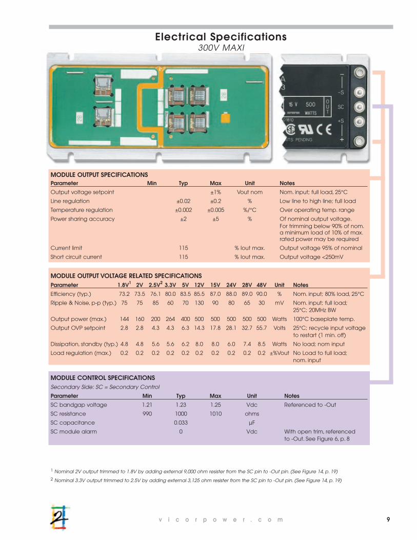
v i c o r p o w e r . c o m 9
MODULE OUTPUT SPECIFICATIONSParameter Min Typ Max Unit Notes
Output voltage setpoint ±1% Vout nom Nom. input; full load, 25°C
Line regulation ±0.02 ±0.2 % Low line to high line; full load
Temperature regulation ±0.002 ±0.005 %/°C Over operating temp. range
Power sharing accuracy ±2 ±5 % Of nominal output voltage.For trimming below 90% of nom.a minimum load of 10% of max.rated power may be required
Current limit 115 % Iout max. Output voltage 95% of nominal
Short circuit current 115 % Iout max. Output voltage <250mV
MODULE OUTPUT VOLTAGE RELATED SPECIFICATIONSParameter 1.8V1 2V 2.5V2 3.3V 5V 12V 15V 24V 28V 48V Unit Notes
Efficiency (typ.) 73.2 73.5 76.1 80.0 83.5 85.5 87.0 88.0 89.0 90.0 % Nom. input; 80% load, 25°C
Ripple & Noise, p-p (typ.) 75 75 85 60 70 130 90 80 65 30 mV Nom. input; full load;25°C; 20MHz BW
Output power (max.) 144 160 200 264 400 500 500 500 500 500 Watts 100°C baseplate temp.
Output OVP setpoint 2.8 2.8 4.3 4.3 6.3 14.3 17.8 28.1 32.7 55.7 Volts 25°C; recycle input voltageto restart (1 min. off)
Dissipation, standby (typ.) 4.8 4.8 5.6 5.6 6.2 8.0 8.0 6.0 7.4 8.5 Watts No load; nom input
Load regulation (max.) 0.2 0.2 0.2 0.2 0.2 0.2 0.2 0.2 0.2 0.2 ±%Vout No Load to full load;nom. input
MODULE CONTROL SPECIFICATIONSSecondary Side: SC = Secondary Control
Parameter Min Typ Max Unit Notes
SC bandgap voltage 1.21 1.23 1.25 Vdc Referenced to -Out
SC resistance 990 1000 1010 ohms
SC capacitance 0.033 µF
SC module alarm 0 Vdc With open trim, referencedto -Out. See Figure 6, p. 8
1 Nominal 2V output trimmed to 1.8V by adding external 9,000 ohm resister from the SC pin to -Out pin. (See Figure 14, p. 19)
2 Nominal 3.3V output trimmed to 2.5V by adding external 3,125 ohm resister from the SC pin to -Out pin. (See Figure 14, p. 19)
Electrical Specifications300V MAXI

10 v i c o r p o w e r . c o m
MODULE INPUT SPECIFICATIONSParameter Min Typ Max Unit Notes
Operating input voltage 250 375 425 Vdc
Undervoltage turn-on 242.5 247.5 Vdc
Undervoltage turn-off 204.7 212.2 Vdc
Overvoltage turn-off/on 429.2 446.3 467.5 Vdc
Input surge withstand 500 Vdc <100ms
MODULE CONTROL SPECIFICATIONSPrimary Side: PC = Primary Control • PR = Parallel
Parameter Min Typ Max Unit Notes
PC bias voltage 5.5 5.7 6.0 Vdc PC current = 1.0mA
PC current limit 1.5 2.1 3 mA PC voltage = 5.5V
PC module disable 2.3 2.6 2.9 Vdc Must be able to sink ≥4mA. See Figure 1, p. 16
PC module enable delay 4 7 ms
PC module alarm 0.5 Vavg UV OV, OT, module fault. See Figures 2, 4, p. 16
PR emitter amplitude 5.7 5.9 6.1 Volts PR load >30ohms, <30pF
PR emitter current 150 mA
PR receiver impedance 375 500 625 ohms 25°C
PR receiver threshold 2.4 2.5 2.6 Volts Minimum pulse width; 20ns
PR drive capability 12 modules >12 modules will require buffer amplifier
MODULE GENERAL SPECIFICATIONSParameter Min Typ Max Unit Notes
Remote sense (total drop) n/a
Isolation voltage (in to out) 3000 Vrms Complies with reinforced insulation requirements
Isolation voltage in to base) 1550 Vrms Complies with basic insulation requirements
Isolation voltage (out to base) 500 Vrms Complies with operational insulation requirements
Isolation resistance (in to out) 10 megohms
Weight 2.1(60) 2.3(66) ounces(grams)
Temperature limiting 100 115 °C See Figures 2, 4, p. 16
Agency approvals UL, CSA, TÜV, BABT, CE, VDE UL1950, CSA950, EN60950, VDE 0805, BS7002IEC60950, (with a fuse in series with the +Input)
Electrical characteristics apply over the full operating range of input voltage, output load (resistive) and baseplatetemperature, unless otherwise specified. All temperatures refer to the operating temperature at the center of the baseplate.
Electrical Specifications375V MICRO

v i c o r p o w e r . c o m 11
MODULE OUTPUT SPECIFICATIONSParameter Min Typ Max Unit Notes
Output voltage setpoint ±1% Vout nom Nom. input; full load, 25°C
Line regulation ±0.02 ±0.2 % Low line to high line; full load
Temperature regulation ±0.002 ±0.005 %/°C Over operating temp. range
Power sharing accuracy ±2 ±5 % 10% to 100% of full load
Programming range 10 110 % Of nominal output voltage.For trimming below 90% of nom.a minimum load of 10% of maximum rated power maybe required
Current limit 115 % Iout max. Output voltage 95% of nominal
Short circuit current 115 % Iout max. Output voltage <250mV
MODULE OUTPUT VOLTAGE RELATED SPECIFICATIONSParameter 1.8V1 2V 2.5V2 3.3V 5V 12V 15V 24V 28V 48V Unit Notes
Efficiency (typ.) 70.0 70.0 75.0 76.5 80.0 83.5 85.0 86.0 86.0 87.5 % Nom. input; 80%load, 25°C
Ripple & Noise, p-p (typ.) 120 110 120 130 120 150 130 135 150 80 mV Nom. input; full load; 25°C; 20MHz BW
Output power (max.) 45 50 57 75 100 150 150 150 150 150 Watts 100°C Baseplate
Output OVP setpoint 2.8 2.8 4.3 4.3 6.3 14.3 17.8 28.1 32.7 55.7 Volts 25°C; recycle input voltageto restart (1 min. off)
Dissipation, standby (typ.) 3.9 3.9 3.9 3.9 4.2 5.4 5.0 5.4 5.0 5.7 Watts No load; nom input
Load regulation (max.) 0.5 0.5 0.4 0.4 0.2 0.2 0.2 0.2 0.2 0.2 ±%Vout No Load to full load; nom. input
MODULE CONTROL SPECIFICATIONSSecondary Side: SC = Secondary Control
Parameter Min Typ Max Unit Notes
SC bandgap voltage 1.21 1.23 1.25 Vdc Referenced to -Out
SC resistance 990 1000 1010 ohms
SC capacitance 0.033 µF
SC module alarm 0 Vdc With open trim, referencedto -Out. See Figure 6, p. 16
1 Nominal 2V output trimmed to 1.8V by adding external 9,000 ohm resister from the SC pin to -Out pin. (See Figure 14, p. 19)
2 Nominal 3.3V output trimmed to 2.5V by adding external 3,125 ohm resister from the SC pin to -Out pin. (See Figure 14, p. 19)
Electrical Specifications375V MICRO

12 v i c o r p o w e r . c o m
MODULE INPUT SPECIFICATIONSParameter Min Typ Max Unit Notes
Operating input voltage 250 375 425 Vdc
Undervoltage turn-on 242.5 247.5 Vdc
Undervoltage turn-off 204.7 212.2 Vdc
Overvoltage turn-off/on 429.2 446.3 467.5 Vdc
Input surge withstand 500 Vdc <100ms
MODULE CONTROL SPECIFICATIONSPrimary Side: PC = Primary Control • PR = Parallel
Parameter Min Typ Max Unit Notes
PC bias voltage 5.5 5.7 6.0 Vdc PC current = 1.0mA
PC current limit 1.5 2.1 3.0 mA PC voltage = 5.5V
PC module disable 2.3 2.6 2.9 Vdc Must be able to sink ≥4mA. See Figure 1, p. 16
PC module enable delay 4 7 ms
PC module alarm 0.5 Vavg UV, OV, OT, module fault. See Figures 2, 4, p. 16
PR emitter amplitude 5.7 5.9 6.1 Volts PR load >30ohms, <30pF
PR emitter current 150 mA
PR receiver impedance 375 500 625 ohms 25°C
PR receiver threshold 2.4 2.5 2.6 Volts Minimum pulse width; 20ns
PR drive capability 12 modules >12 modules will require buffer amplifier
MODULE GENERAL SPECIFICATIONSParameter Min Typ Max Unit Notes
Remote sense (total drop) 0.5 Vdc 0.25V/leg (sense leads must be closed)
Isolation voltage (in to out) 3000 Vrms Complies with reinforced insulation requirements
Isolation voltage in to base) 1550 Vrms Complies with basic insulation requirements
Isolation voltage (out to base) 500 Vrms Complies with operational insulation requirements
Isolation resistance (in to out) 10 megohms
Weight 3.7(104) 4(112) ounces(grams)
Temperature limiting 100 115 °C See Figures 2, 4, p. 16
Agency approvals UL, CSA, TÜV, BABT, CE, VDE UL1950, CSA950, EN60950, VDE 0805, BS7002IEC60950, (with a fuse in series with the +Input)
Electrical characteristics apply over the full operating range of input voltage, output load (resistive) and baseplatetemperature, unless otherwise specified. All temperatures refer to the operating temperature at the center of the baseplate.
Electrical Specifications375V MINI

v i c o r p o w e r . c o m 13
MODULE OUTPUT SPECIFICATIONSParameter Min Typ Max Unit Notes
Output voltage setpoint ±1% Vout nom Nom. input; full load, 25°C
Line regulation ±0.02 ±0.2 % Low line to high line; full load
Temperature regulation ±0.002 ±0.005 %/°C Over operating temp. range
Power sharing accuracy ±2 ±5 % 10 to 100% of full load
Programming range 10 110 % Of nominal output voltage.For trimming below 90% of nom.a minimum load of 10% of maximum rated power may be required
Current limit 115 % Iout max. Output voltage 95% of nominal
Short circuit current 115 % Iout max. Output voltage <250mV
MODULE OUTPUT VOLTAGE RELATED SPECIFICATIONSParameter 1.8V1 2V 2.5V2 3.3V 5V 12V 15V 24V 28V 48V Unit Notes
Efficiency (typ.) 71.0 72.0 75.0 77.7 81.5 84.0 86.0 87.0 87.5 89.0 % Nom. input; 80% load, 25°C
Ripple & Noise, p-p (typ.) 100 100 100 100 110 150 140 190 130 170 mV Nom. input; full load;25°C; 20MHz BW
Output power (max.) 90 100 114 150 200 300 300 300 300 300 Watts 100°C baseplate
Output OVP setpoint 2.8 2.8 4.3 4.3 6.3 14.3 17.8 28.1 32.7 55.7 Volts 25°C; recycle input voltageto restart (1 min. off)
Dissipation, standby (typ.) 4.8 4.8 5.1 5.1 5.4 5.5 5.6 4.5 5.5 5.2 Watts No load; nom input
Load regulation (max.) 0.3 0.3 0.2 0.2 0.2 0.3 0.3 0.3 0.3 0.4 ±%Vout No Load to full load;nom. input
MODULE CONTROL SPECIFICATIONSSecondary Side: SC = Secondary Control
Parameter Min Typ Max Unit Notes
SC bandgap voltage 1.21 1.23 1.25 Vdc Referenced to -Out
SC resistance 990 1000 1010 ohms
SC capacitance 0.033 µF
SC module alarm 0 Vdc With open trim, referencedto -Out. See Figure 6, p. 16
1 Nominal 2V output trimmed to 1.8V by adding external 9,000 ohm resister from the SC pin to -Out pin. (See Figure 14, p. 19)
2 Nominal 3.3V output trimmed to 2.5V by adding external 3,125 ohm resister from the SC pin to -Out pin. (See Figure 14, p. 19)
Electrical Specifications375V MINI

14 v i c o r p o w e r . c o m
MODULE INPUT SPECIFICATIONSParameter Min Typ Max Unit Notes
Operating input voltage 250 375 425 Vdc
Undervoltage turn-on 242.5 247.5 Vdc
Undervoltage turn-off 204.7 212.2 Vdc
Overvoltage turn-off/on 429.2 446.3 467.5 Vdc
Input surge withstand 500 Vdc <100ms
MODULE CONTROL SPECIFICATIONSPrimary Side: PC = Primary Control • PR = Parallel
Parameter Min Typ Max Unit Notes
PC bias voltage 5.5 5.7 6.0 Vdc PC current = 1.0mA
PC current limit 1.5 2.1 3.0 mA PC voltage = 5.5V
PC module disable 2.3 2.6 2.9 Vdc Must be able to sink ≥4mA. See Figure 1, p. 16
PC module enable delay 4 7 ms
PC module alarm 0.5 Vavg UV, OV, OT, module fault. See Figures 2, 4, p. 16
PR emitter amplitude 5.7 5.9 6.1 Volts PR load >30ohms, <30pF
PR emitter current 150 mA
PR receiver impedance 375 500 625 ohms 25°C
PR receiver threshold 2.4 2.5 2.6 Volts Minimum pulse width; 20ns
PR drive capability 12 modules >12 modules will require buffer amplifier
MODULE GENERAL SPECIFICATIONSParameter Min Typ Max Unit Notes
Remote sense (total drop) 0.5 Vdc 0.25V/leg (sense leads must be closed)
Isolation voltage (in to out) 3000 Vrms Complies with reinforced insulation requirements
Isolation voltage in to base) 1550 Vrms Complies with basic insulation requirements
Isolation voltage (out to base) 500 Vrms Complies with operational insulation requirements
Isolation resistance (in to out) 10 megohms
Weight 7.3(210) 8(227) ounces(grams)
Temperature limiting 100 115 °C See Figures 2, 4, p. 16
Agency approvals UL, CSA, TÜV, BABT, CE, VDE UL1950, CSA950, EN60950, VDE 0805, BS7002IEC60950, (with a fuse in series with the +Input)
Electrical characteristics apply over the full operating range of input voltage, output load (resistive) and baseplatetemperature, unless otherwise specified. All temperatures refer to the operating temperature at the center of the baseplate.
Electrical Specifications375V MAXI

v i c o r p o w e r . c o m 15
MODULE OUTPUT SPECIFICATIONSParameter Min Typ Max Unit Notes
Output voltage setpoint ±1% Vout nom Nom. input; full load, 25°C
Line regulation ±0.02 ±0.2 % Low line to high line; full load
Temperature regulation ±0.002 ±0.005 %/°C Over operating temp. range
Power sharing accuracy ±2 ±5 % Of nominal output voltage.For trimming below 90% of nom.a minimum load of 10% of max.rated power may be required
Current limit 115 % Iout max. Output voltage 95% of nominal
Short circuit current 115 % Iout max. Output voltage <250mV
MODULE OUTPUT VOLTAGE RELATED SPECIFICATIONSParameter 1.8V1 2V 2.5V2 3.3V 5V 12V 15V 24V 28V 48V Unit Notes
Efficiency (typ.) 73.0 74.5 76.0 80.0 83.5 85.7 87.0 88.0 89.0 90.0 % Nom. input; 80% load, 25°C
Ripple & Noise, p-p (typ.) 70 70 70 80 102 1320 90 92 160 50 mV Nom. input; full load;25°C; 20MHz BW
Output power (max.) 144 160 200 264 400 600 600 600 600 500 Watts 100°C baseplate temp.
Output OVP setpoint 2.8 2.8 4.3 4.3 6.3 14.3 17.8 28.1 32.7 55.7 Volts 25°C; recycle input voltageto restart (1 min. off)
Dissipation, standby (typ.) 5.0 5.0 4.9 4.9 5.0 8.7 8.0 8.5 8.0 6.0 Watts No load; nom input
Load regulation (max.) 0.2 0.2 0.2 0.2 0.2 0.2 0.2 0.2 0.2 0.2 ±%Vout No Load to full load;nom. input
MODULE CONTROL SPECIFICATIONSSecondary Side: SC = Secondary Control
Parameter Min Typ Max Unit Notes
SC bandgap voltage 1.21 1.23 1.25 Vdc Referenced to -Out
SC resistance 990 1000 1010 ohms
SC capacitance 0.033 µF
SC module alarm 0 Vdc With open trim, referencedto -Out. See Figure 6, p. 16
1 Nominal 2V output trimmed to 1.8V by adding external 9,000 ohm resister from the SC pin to -Out pin. (See Figure 14, p. 19)
2 Nominal 3.3V output trimmed to 2.5V by adding external 3,125 ohm resister from the SC pin to -Out pin. (See Figure 14, p. 19)
Electrical Specifications375V MAXI

16 v i c o r p o w e r . c o m
Module Enable/DisableThe module may be disabled by pulling PC below2.3V with respect to -Input. This may be done with anopen collector transistor, relay, or optocoupler.Multiple converters may be disabled with a singletransistor or relay either directly or via “OR’ing”diodes. See Figure 1
Primary Auxiliary SupplyAt 5.7V, PC can source up to 1.5 mA. In the exampleshown in Figure 3, PC powers a LED to indicate themodule is enabled.
Module AlarmThe module contains “watchdog” circuitry whichmonitors input voltage, operating temperature andinternal operating parameters. In the event that anyof these parameters are outside of their allowableoperating range, the module will shut down and PCwill go low. PC will periodically go high and themodule will check to see if the fault (as an example,overtemperature) has cleared. If the fault has notbeen cleared, PC will go low again and the cycle willrestart. The SC pin will go low in the event of a faultand return to its normal state after the fault has beencleared. See Figures 2 and 4
1. Module Enable/Disable Figure 2. PC/SC module alarm logic (Micro Inset)
Figure 3. LED on-state indicator Figure 4. PC/SC module alarm timing
Figure 5. Isolated on-state indicator Figure 6. Secondary side on-state (Micro inset)
+In
PC
PR
–In
Disable
Disable = PC <2.3V
+Out
+S
SC
–S
–Out
+In
PC
PR
–In
Input Undervoltage
2-20ms typ.f (VIN)
AutoRestart
5.7Vdc(0-3mA)
50Ω
SW2 SW3
1.23Vdc 6K
1K
SW1
SW1, 2, & 3shown in
"Fault" position
Input OvervoltageOvertemperatureModule Faults
+In
PC
PR
–In
4kΩ "Module Enabled"
+In
PC
PR
–In
Optocoupler
4kΩ
2-20ms typ.
Fault
SC
PC
1.23V
5.7V40µs typ.
Alarm
1.00V
+Out
+S
SC
–S
–Out
Alarm
1.00V
+Out
SC
–Out
Input UndervoltageInput OvervoltageOver TemperatureModule Faults
2-20ms typ.f(VIN)
AutoRestart
5.7Vdc(0-3mA)
50Ω
SW2 SW3
1.23Vdc
6K
1K
SW1
SW1, 2, & 3 shownin "Fault" position
+Out
SC
–Out
+In
PC
PR
–In
Control FunctionsPrimary Control (PC Pin)
v i c o r p o w e r . c o m 17
Parallel Bus PR Pin
Parallel OperationA unique feature has been designed into Vicor’s 2nd Generation converter modules which facilitatesparallel operation for power expansion or redundancy.The “PR” pin is a bi-directional port that transmits andreceives information between modules. The pulsesignal on the parallel (PR) bus serves to synchronizethe high frequency switching of each converterwhich in turn forces them to load share. These modulespossess the ability to arbitrate the leadership role; i.e.,a democratic array. The module that assumescommand transmits the sync pulse on the parallel buswhile all other modules on the bus listen.
Compatible interface architectures include the following:DC coupled single-wire interface. All PR pins aredirectly connected to one another. This interfacesupports current sharing but is not fault tolerant. MinusIn pins must be tied to the same electric potential.
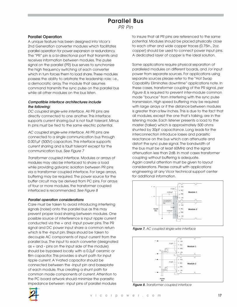
AC coupled single-wire interface. All PR pins areconnected to a single communication bus through0.001µF (500V) capacitors. This interface supportscurrent sharing and is fault tolerant except for thecommunication bus. See Figure 7
Transformer coupled interface. Modules or arrays ofmodules may also be interfaced to share a load while providing galvanic isolation between PR pinsvia a transformer coupled interface. For large arrays,buffering may be required. The power source for thebuffer circuit may be derived from PC pins. For arraysof four or more modules, the transformer coupledinterfaced is recommended. See Figure 8
Parallel operation considerationsCare must be taken to avoid introducing interferingsignals (noise) onto the parallel bus as this mayprevent proper load sharing between modules. Onepossible source of interference is input ripple currentconducted via the + and -Input power pins. The PRsignal and DC power input share a common returnwhich is the -Input pin. Steps should be taken to decouple AC components of input current from theparallel bus. The input to each converter (designatedas + and - pins on the input side of the module)should be bypassed locally with a 0.2µF ceramic orfilm capacitor. This provides a shunt path for inputripple current. A Y-rated capacitor should beconnected between the -Input pin and baseplate of each module, thus creating a shunt path forcommon mode components of current. Attention tothe PC board artwork should minimize the parasiticimpedance between -Input pins of parallel modules
to insure that all PR pins are referenced to the samepotential. Modules should be placed physically closeto each other and wide copper traces (0.75in., 2oz.copper) should be used to connect power input pins.A dedicated layer of copper is the ideal solution.
Some applications require physical separation ofparalleled modules on different boards, and /or inputpower from separate sources. For applications usingseparate sources please refer to the “Hot SwapCapability Eliminates downtime” applications note. Inthese cases, transformer coupling of the PR signal, perFigure 8, is required to prevent inter-module commonmode “bounce” from interfering with the sync pulsetransmission. High speed buffering may be requiredwith large arrays or if the distance between modulesis greater than a few inches. This is due to the fact thatall modules, except the one that’s talking, are in thelistening mode. Each listener presents a load to themaster (talker) which is approximately 500 ohmsshunted by 30pF capacitance. Long leads for theinterconnection introduce losses and parasiticreactance on the bus which can attenuate anddistort the sync pulse signal. The bandwidth of the bus must be at least 60MHz and the signalattenuation less than 2dB. In most cases transformercoupling without buffering is adequate.Again careful attention must be given to layoutconsiderations. Please consult with applicationsengineering at any Vicor technical support center for additional information.
Figure 7. AC coupled single-wire interface
Figure 8. Transformer coupled interface
0.2µF
Low inductanceground plane orbus
+In
PC
PR
–In
+In
PC
PR
–In
Module 2
Module 10.001µF
0.2µF
0.001µF
+
ParallelBus
–
0.2µF+In
PC
PR
–In
+In
PC
PR
–In
Module 2
Module 1
0.2µF
T1
T2
ParallelBus
+
–
+
–
12
34
56
56

18 v i c o r p o w e r . c o m
PR Pin ConsiderationsWhen paralleling modules it is important that the PR signal is communicated to all modules within theparallel array. Modules which do not receive a PR pulse in a parallel array will not current share and may be damaged by running in an overpower condition.
All modules in an array must be of the same type.
Series connection of outputs is generallyaccomplished without connecting the PR pin andallowing each module to regulate its own outputvoltage. Since the same current passes through theoutput of each module with the series connection,power sharing is inherent. Series connection of inputsrequires special precautions, please contactapplications engineering for assistance.
The + and -Output pins of modules connected in aparallel array must never be allowed to become
open circuited from the output bus or permanentdamage to the module may result.
Figure 13. Resister values for Micro voltage drop compensation.
Control Functions and Output ConsiderationsParallel Operation (PR Pin)
Parallel OperationThe PR pin supports paralleling for increased powerwith N+1 (N+M) redundancy and phased arraycapability. Modules of the same input voltage,output voltage, and power level will current share if
all PR pins are suitably interfaced. Figures 9 and 10show connections for the Maxi and Mini modules;Figures 11 and 12 show connections for Micro modules.
Figure 9. N+1 module array output connections (Maxi and Mini) Figure 10. OR”ing diodes connections (Maxi and Mini)
Module 2
Module 1
Module N+1
+Out
+SSC–S
–Out
+Out
+SSC–S
–Out
+Out
+SSC–S
–Out
Load
+S
–S
+S
–S
+S
–S
+Out
+S
SC
–S
–Out +Sense fromother modules
in the array
Figure 11. N+1 module array output connections (Micro) Figure 12. Voltage drop compensation (Micro)
Vo R1 R2 R3 R4 Unit1.8 1K 500 9K 550 Ω2.0 1K 500 N/R 750 Ω2.2 1K 500 1.0K 1.00K Ω2.5 1K 500 3.125K 1.25K Ω3.3 1K N/R N/R 2.05K Ω5.0 10K N/R N/R 3.75K Ω
12.0 10K N/R N/R 10.8K Ω15.0 10K N/R N/R 13.75K Ω24.0 10K N/R N/R 22.75K Ω28.0 10K N/R N/R 26.75K Ω48.0 * 10K N/R N/R 46.75K Ω
The LM10 is rated for a supply voltage of 45Vdc max. If theoutput voltage exceeds this rating use a 5 to 15V zener diodefrom pin 7 of the LM10 to V–. A series resistor should beconnected from V+ to the cathode of the zener diode. Theresistor value should be selected to set the zener current to 1mA.
+Out
SC
–Out
+Out
SC
–Out
+Out
SC
–Out
LOAD
Plane
GroundPlane
R1
4
27
6LoadLM10
+Out
SC
–Out
R2
R3
13
8
0.001 µF
1.05KΩ
200Ω
R4
1.2KΩ
• The +Out and -Out power buses should be designed to minimize and balance parasitic impedance from each module output to the load.
• The +Sense pins should be tied to the same point on the +Out power bus; the -Sense pins should be tied to the same point on the -Out power bus.
• At the discretion of the power system designer, a subset of all modules within an array may be configured as slaves by shorting SC to -S.
• OR’ing diodes may be inserted in series with the +OUT pins of each module to provide module output fault tolerance.
• The +Out and -Out power buses should be designed to minimize and balance parasitic impedance from each module output to the load.
• At the discretion of the power system designer, a subset of all modules within an array may be configured as slaves by shorting SC to -Out.
• Do not use output OR’ing diodes with parallel arrays of MicroMods.
See Figure 13.
*

v i c o r p o w e r . c o m 19
Control FunctionsSecondary Control (SC Pin)
SC Pin and Output Voltage TrimmingCircuits such as OP-Amps and D/A converters whichdirectly drive the SC pin should be designed to limitthe applied voltage to the SC pin. It is also importantto consider voltage excursions that may occurduring initialization of the external circuitry. Theexternal circuit must be referenced to the -S pin (-Out on Micro).
For systems which require an adjustable outputvoltage, it is good practice to limit the adjustmentrange to a value only slightly greater than thatrequired. This will increase the adjustment resolutionwhile reducing noise pickup.
Contact Applications Engineering if the module is tobe dynamically trimmed.
Trim values calculated automaticallyTrimming resistor calculators are available onVicor’s web site at www.vicorpower.com/tools orby requesting a copy of Vicor’s ApplicationsManual on CD ROM.
Resistor values can be calculated for fixed trim up,fixed trim down and for variable trim up or down.
In addition to trimming information, the web siteand the applications manual on CD ROM alsoincludes design tips, applications circuits, EMCsuggestions, thermal design guidelines and PDFdata sheets for all Vicor products.
Output Voltage ProgrammingThe output voltage of the converter can be adjustedor programmed via fixed resistors, potentiometers orvoltage DACs. See Figures 14 and 15
Trim Down1. This converter is NOT a constant power device;
it has a constant current limit. Hence, available output power is reduced by the same percentage that output voltage is trimmed down. Do not exceed maximum rated output current.
2. The trim down resistor must be connectedto the -Sense pin (-Out pin on a Micro).
Trim Up1. The converter is rated for a maximum delivered
power. To ensure that maximum rated power is not exceeded, reduce maximum output current by the same percentage increase in output voltage.
2. The trim up resistor must be connected to the+Sense pin (+Out pin on a Micro).
3. Do not trim the converter above maximum trim range (+10%) or the output over voltage protection circuitry may be activated.
Figure 14. Output voltage trim down circuit (Micro inset) Figure 15. Output voltage trim up circuit (Micro inset)
Load
+Out
+S
SC
–S
–Out
RDTrim Down
ErrorAmp
1kΩ
1.23V
0.033µF
+Out
+S
SC
–S
–Out
RUTrim Up LoadError
Amp
1kΩ
1.23V
0.033µF
Load
RDTrim Down
ErrorAmp
1kΩ
1.23V
0.033µF
+Out
SC
–Out
RUTrim Up
LoadErrorAmp
1kΩ
1.23V
0.033µF
+Out
SC
–Out
RD (ohms) = 1,000 VoutVnom - Vout
RU (ohms) = 1,000 (Vout-1.23) Vnom -1,0001.23(Vout - Vnom)

20 v i c o r p o w e r . c o m
Do's and Don'ts and General Topics
Safety ConsiderationsFusingSafety agency conditions of acceptability requirethat the module (+) input terminal be fused and thebaseplate of the converter be connected to earthground. The following table lists the acceptable fusetypes and current rating for the 300V and 375V inputfamilies of DC-DC converters.
The location of the fuse must be in series with thepositive (+) input lead. Fusing the negative input leaddoes not provide adequate protection as the PRand PC terminals of the converter are referenced tothe -Input. If a fuse located in the -Input lead were toopen, the PR and PC terminals would rise to thepotential of the +Input. This could damage anyconverter or circuitry connected to these pins. Thefuse should not be located in an area with a highambient temperature as this will lower the currentcarrying rating of the fuse.
Thermal and Voltage HazardsVicor component power products are intended tobe used within protective enclosures. Vicor DC-DCconverters can work comfortably at baseplatetemperatures which could be harmful if contacteddirectly. Voltages and high currents (energy hazard)present at the terminals and circuitry connected tothem may pose a safety hazard if contacted or if stray current paths develop. Systems withremovable circuit cards or covers which may expose the converter(s) or circuitry connected tothem should have proper guarding to avoidhazardous conditions.
PC PinThe PC pin should only be used to disable the module, provide a bias to input referenced circuitryor communicate status of the module.
The PC pin is referenced to the -Input pin. All circuitswhich connect to the PC pin must use the -Input asthe reference. Do not break the connection
between the -Input and the circuitry connected tothe PC pin or damage to the module will result.
Circuits which derive their power from the PC pinmust not exceed 1.5mA.
Do not do not drive the PC pin with external circuitry.
Do not attempt to control the output of the converter by PWM modulation of the PC pin.
For applications where the converter will be disabled on a regular basis or where capacitance is added to this pin, please contact Vicor applications engineering.
High Power Arrays and PR PinTo simplify the implementation of large arrays, a subset of modules within the parallel array may beconfigured as boosters by connecting the SC pin tothe -Sense lead. Modules which are connected asboosters can not assume the role of drivers for N+Mredundant arrays. Modules configured as boostersmay be locally sensed.
Each module within the parallel array must be properly bypassed with capacitors. Film or ceramictypes should be used across the input of the moduleand between each input lead and the baseplate.Modules which have input sources which are notconnected to SELV sources should use X-ratedcapacitors across the input and Y-rated capacitorsfrom each lead to the baseplate. When in doubtabout capacitor safety approvals, always consultwith the governing safety regulatory agency or Vicorapplications engineering.
A maximum of 12 modules may be connected inparallel. Please contact Vicor applicationsengineering for recommendations for larger arrays.
The PR pin is referenced to the -Input pin, thereforeall modules within the array must have a commonlow impedance connection between each -Inputpin. Special precautions are necessary if a PWB is notused for interconnection of modules as the wiringimpedance can be significant. Do not allow theconnection between the -Input pin and the -Inputbus to become disconnected or damage to the module will result.
Coupling transformers should be used to transmit the PR pulse if long distances between each moduleare anticipated or if the interconnection impedanceof the -Input leads is high or questionable. PR coupling transformers should be used if the PR pulseleaves the PWB. For example, an array constructedof multiple circuit cards plugged into a backplane
Fuse Ratings and Recommended Types
Package Output Fuse for Fuse forVoltage 300Vin 375Vin
Maxi 2, 3.3 Buss PC Buss PCTron 3A Tron 5A
Maxi 5, 12, 15, Buss PC Buss PC24, 28, 48 Tron 5A Tron 5A
Mini 2, 3.3, 5, 12, Buss PC Buss PC15, 24, 28, 48 Tron 3A Tron 5A
Micro 2, 3.3, 5, 12, Buss PC Buss PC15, 24, 28, 48 Tron 3A Tron 3A
v i c o r p o w e r . c o m 21
with a number of converters on each card wouldbenefit by having a PR coupling transformer at theentry point of each card, however no couplingtransformer would be required between eachconverter on the card. Do not externally drive the PR pin. Connection to this pin is limited to Vicormodules only. Refer to page 10, "Control Functionsand Output Considerations" for additionalinformation on parallel operation.
Input Source ImpedanceThe impedance of the source feeding the input ofthe module directly affects both the stability andtransient response of the module. In general thesource impedance should be lower than the inputimpedance of the module by a factor of ten.
To calculate the required source impedance, use thefollowing formula:
Z = 0.1 x (VLL)2 / Pin where:
Z is required input impedanceVLL is the low line input voltagePin is the input power of the module
In addition for the 300V and 375V input families ofconverters a minimum of 2uF should be used at theinput of each converter in applications where thedistance between the converter and holdupcapacitors exceed six inches (6").
Filters which precede the converter module shouldbe well damped to prevent ringing when the inputvoltage is applied or the load on the output of theconverter is abruptly changed.
Input Transients and SurgesThe voltage applied to the input of the module mustnot exceed the ratings outlined in the data sheet.The rate of rise for the 300V and 375V input familiesshould be limited to 10V/µS. Protection devices suchas Zener diodes and MOV’s should be used toprotect the module from short duration transients.These shunt protection devices are only effective ifthe source impedance is high relative to theimpedance of the protection device when it isconducting. For voltage surges where the abnormalvoltage is present for a long period of time, shuntprotection devices can easily be damaged by thepower dissipated. For this type of condition a voltagelimiter in series with the input of the module may bethe best solution. Vicor Applications Engineering canassist in recommending the appropriate type ofprotection for the module.
Sense Leads (Mini and Maxi only)The sense leads of the module must always terminate either directly to the output pins (local sensing) or at the load (remote sensing).When remote sensing is used, the wiring impedancein combination with the load impedance can causesignificant loss of phase margin and result in oscillation and possible damage to the module,poor transient response, or activation of the outputovervoltage protection. Long sense leads mayrequire a compensation circuit for stability.
Protection circuitry is required for reversed senseleads. Please contact Vicor Applications Engineeringfor specific recommendations.
Do not exceed 1V between -S and -Out leads. This isan important consideration if the converter is used ina Hot Swap application. OR'ing diodes, if used,should be located in the +Output lead to avoidexceeding this rating.
Do not exceed the rated power of the converter. Thetotal of the power consumed by the load plus thepower lost in conductors from the converterto the load must be less than the output power rating of the converter.
Output ConnectionsFor systems which charge batteries, subject the module to dynamic loading, or loads which havelarge reactive components, please contact VicorApplications Engineering to discuss your application.
Do not externally drive the output of the modulehigher than its nominal or trimmed setpoint voltage.
Modules which are used to charge batteries shoulduse a diode in series with the output of the module.The charge current must be externally controlled toinsure that the module is not operated in excess of itspower rating.
Current carrying conductors should be sized tominimize voltage drops.
Do not use output OR’ing diodes with parallelarrays of micro modules.
Absolute Maximum RatingsPlease consult individual module data sheets formaximum rating concerning pin-pin voltages,isolation, temperature and mechanical ratings.Refer to "Control Functions, Secondary Control" on page 11 for application information regardingoutput voltage adjustment.
22 v i c o r p o w e r . c o m
Filtering and Transient ProtectionEnhanced Common Mode and Differential Mode FIltering
All switching power supplies generate potentiallyinterfering signals as a result of high frequency, highpower switching. The Vicor power convertertopology, to a large extent, addresses the problem atthe source by the use of a quasi-resonant, zerocurrent switching topology. The switching currentwaveform is a half sine wave that generates far lessconducted and radiated noise in both frequencyspectrum and magnitude. EMI filtering, if properlydesigned and implemented, reduce the magnitudeof conducted noise an additional 40-60dB, and as aresult, the noise radiated by the power conductors isreduced proportionally.
Conducted noise on the input power lines can occuras either differential mode or common mode noisecurrents. Differential mode noise appears across theinput conductors at the fundamental switchingfrequency and its harmonics. Common mode noise ismeasured between the converter's input conductorsand ground, having mostly high-frequency content.
Some basic guidelines to follow for successful EMIfiltering are as follows:
1. Keep current loops small. The ability of a conductor to couple energy by induction and radiation is reduced accordingly.
2. For conductor pairs, use wide (low Z) copper traces aligned above and below each other.
3. Locate filters at the source of interference; i.e., the power converter.
4. Filter component values should be chosen with consideration given to the desired frequency rangeof attenuation. For example, capacitors are self resonant at some frequency, beyond which they
look inductive. Keep bypass capacitor leads as short as possible.
5. Locate components on the board with consideration given to proximity of noise sources to potentially susceptible circuits.
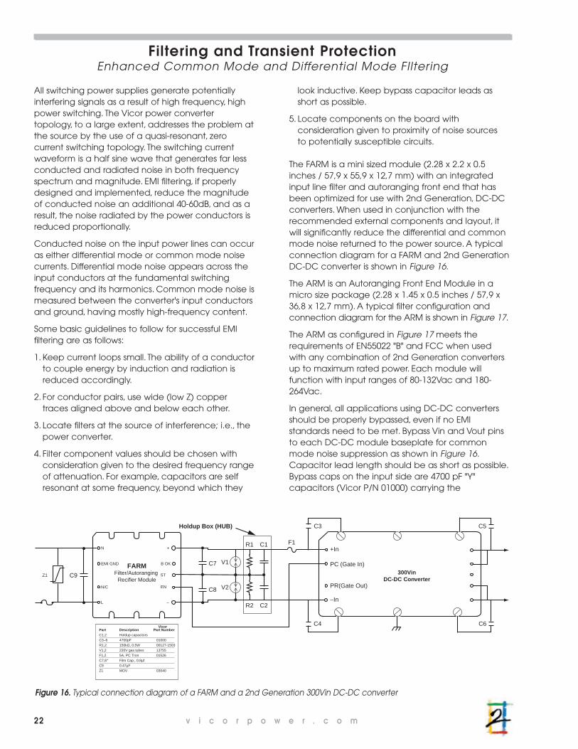
The FARM is a mini sized module (2.28 x 2.2 x 0.5inches / 57,9 x 55,9 x 12,7 mm) with an integratedinput line filter and autoranging front end that hasbeen optimized for use with 2nd Generation, DC-DCconverters. When used in conjunction with therecommended external components and layout, itwill significantly reduce the differential and commonmode noise returned to the power source. A typicalconnection diagram for a FARM and 2nd GenerationDC-DC converter is shown in Figure 16.
The ARM is an Autoranging Front End Module in amicro size package (2.28 x 1.45 x 0.5 inches / 57,9 x36,8 x 12,7 mm). A typical filter configuration andconnection diagram for the ARM is shown in Figure 17.
The ARM as configured in Figure 17 meets therequirements of EN55022 "B" and FCC when usedwith any combination of 2nd Generation convertersup to maximum rated power. Each module willfunction with input ranges of 80-132Vac and 180-264Vac.
In general, all applications using DC-DC convertersshould be properly bypassed, even if no EMIstandards need to be met. Bypass Vin and Vout pinsto each DC-DC module baseplate for commonmode noise suppression as shown in Figure 16.Capacitor lead length should be as short as possible.Bypass caps on the input side are 4700 pF "Y"capacitors (Vicor P/N 01000) carrying the
+In
PC (Gate In)
PR(Gate Out)
–In
Vicor DC-DCConverter
R1
R2
C1
C2
V1
V2
C3
C4
F1
C7
C8
Holdup Box (HUB)
FARMFilter/Autoranging
Recifier Module
N
EMI GND
N/C
L
+
B OK
ST
EN
–
Z1
C5
C6PartC1,2C3–6R1,2V1,2F1,2C7,8C9Z1
DescriptionHoldup capacitors4700pF150kΩ, 0.5W220V gas tubes5A, PC TronFilm Cap., 0.8µf0.47µFMOV
VicorPart Number 01000 00127-1503 13755 01526
03040
*
C9
Figure 16. Typical connection diagram of a FARM and a 2nd Generation 300Vin DC-DC converter
300VinDC-DC Converter

v i c o r p o w e r . c o m 23
appropriate safety agency approval. Bypass caps onthe output side are 0.01µF ceramic capacitors ratedat 500V (Vicor P/N 01501). All baseplates must beconnected to the protective earth conductor andequipment chassis.
EMl can be very application dependent. A packagedfilter and front end accessory module may notalways be the right answer, and the general practiceof bypassing Vin and Vout may not produce optimalresults.You may have to adjust the values dependingon the spectral characteristics and magnitudes ofcommon mode and differential mode noise.
Input transient/surge suppression should be used inmost applications where source transients may beinduced by load changes, blown fuses, heavymachinery, lightning strikes on the power grid, etc.The level of transient suppression required willdepend on the expected severity of the transients,and EMC requirements. A TRANSORBTM or MOV (Z1)will provide transient suppression and act as avoltage clamp for input spikes. The device voltagerating should be chosen above high line voltagelimits to avoid conducting during normal operationwhich would result in overheating.
+In
PC (Gate In)
PR(Gate Out)
–In
Vicor DC-DCConverter
R5
R6
C5
C6
V1
V2
C7
C8
F1
C9
C10
Holdup Box (HUB)
820µF HUB820-S, 2200µF HUB2200-S 1200µF HUB1200-S, 2700µF HUB2700-S1800µF HUB1800-S, 3300µF HUB3300-S
C11
C12
C2
R4
C4
N
L
E
L1R3
L2
R1
R2
L3
C1
C3F1
Z1
Part
C1
C2, C3
C4
C5,C6
C7, C8
C9, C10*
C11, C12
F1
F2
Description
1.0µF
4700pF
0.15µF
Holdup capacitors
4700pF
Film Cap., 0.8µF
.01µF
12A fuse
5A, PC Tron
VicorPart Number
02573
01000
03269
01000
01501
05147
01526
N
ST
L
+V
BOKEN
–V
VI-ARM
Part
L1, L2
L3
R1, R2
R3, R5, R6
R4
V1, V2
Z1
Description
27µH
1.3mH
10Ω
150kΩ, 0.5W
2.2Ω
220V gas tubes
MOV
VicorPart Number
14563
15016
00127-1503
05147
13755
03040
* Required if C1 & C2 are located more than 6 inches from output of ARM.
17. Typical line filter, ARM and 300Vin DC-DC connection diagram
18. Conducted noise plot: FARM with V300A15C500A
300VinDC-DC Converter

24 v i c o r p o w e r . c o m
Test & MeasurementEfficiency
Efficiency is defined as the ratio of delivered outputpower to converter input power and is a basic figureof merit that can be used to relate power dissipationdirectly to converter output power. It is a function ofinput voltage, input voltage range, temperature,output voltage and output power or current.Efficiency affects the design and size of the coolingsystem as well as the power system componentsneeded to power the system – fuses, filters,batteries, etc.
Efficiency is also a key parameter in battery backedup systems found in central offices, customerpremises and remote sites. The higher the efficiency,the longer a system will continue to operate from a
battery given a fixed Ampere-hour capacity. Asystem with an efficiency rating of 85% will reducethe dissipation by approximately a factor of 1/2 versus a system with 75% efficiency.
The accuracy of efficiency measurements, like other parameters, are affected by technique andequipment. Separate DVMs for input and outputvoltage measurements are required as are accuratecurrent measuring devices for both input and output current.
Basic Measurement Technique1. Make all connections unpowered.
2. Set Vin at 300Vdc for a 300V family module
(375Vdc for a 375V family module) as measured at the input pins.
3. Set electronic load for full load current and record measurement.
4. Measure input current.
5. Measure output voltage at output pins andrecord measurement.
6. Calculate efficiency
Efficiency Measurement
DO
DON'T
-Out
-S
SC
+S
+Out+In
PC
PR
-In
2nd GenerationDC-DC Converters
48Vdc Input
+– DVM ELECTRONIC
LOADDVMELECTRONICPOWER SUPPLY
-Out
-S
SC
+S
+Out+In
PC
PR
-In
2nd GenerationDC-DC Converters
48Vdc Input
+–DVM DVM
Eff. (in %) = Vout x Iout x 100Vin x Iin
2nd Generation300Vdc and 375Vdc Input
DC-DC Converters
2nd Generation300Vdc and 375Vdc Input
DC-DC Converters

v i c o r p o w e r . c o m 25
Test & MeasurementRegulation
Regulation is the ability of a power supply or aDC-DC converter to maintain an output voltagewithin a specified tolerance independent ofchanging conditions of input voltage and /or outputload. Regulation measurements usually involvechanging input voltage or output load conditionswhile measuring the output voltage. Measurementtechniques can adversely affect the accuracy of themeasurement, so the following guidelines should beobserved.
Guidelines• Make all voltage measurements as close to the
Input and Output pins as possible
• Use an electronic load with appropriate sizedconductors
• Do not use the integral volt meter of the electronic load to measure output voltage; use a separate DVM
• Be certain to properly cool the DC-DC converteras the tests are run; a small cooling fan directedon the module is usually sufficient for tests of ashort duration
• Make certain to use test equipment in goodworking order and properly calibrated
• Make all connections including local sense ifapplicable, observing correct polarity beforeturning on voltage source
Measurement Procedure Line Regulation1. Set input voltage for 300Vdc, or 375Vdc
(depending on family).
2. Set output load for 75% of maximum ratedload current.
3. Measure output voltage and record.
4. Reduce input voltage to minimum (180 for 300V family, or 250 for 375V family) and measure output voltage and record result.
5. Increase input voltage to maximum(375 for 300V family, or 425 for 375V family) and measure output voltage and record result.
The difference in readings is a measure of lineregulation as a percent of output voltage(at nominal input voltage).Record:Vout ______ @ 75% load, 300/375Vdc inputVLL ______ @ 75% load, 180/250Vdc inputVHL ______ @ 75% load, 375/3425Vdc input
Then:100 x (VoutLL - VoutHL) /Vset point = % Line Regulation
Measurement Procedure Load Regulation1. Return all settings to nominal (i.e. 300Vdc input,
75% maximum load).
2. Measure and record output voltage.
3. Increase the electronic load setting to 100% ofrated output.
4. Measure and record output voltage.
5. Decrease the load setting to zero Amps.
6. Measure and record output voltage.
The difference in readings is a measure of loadregulation as a percent of output voltage atrated load.Record:Vout ______ @ 75% load, nominal inputVNL ______ @ 0% load, nominal inputVFL ______ @ 100% load, nominal inputs
Then:(VoutNL – VoutFL) /Vset point x 100 = % Load Regulation

26 v i c o r p o w e r . c o m
Test & MeasurementOutput Ripple and Noise
Output ripple & noise is defined as the sum ofperiodic and random deviations (PARD) present onthe DC output. The periodic (ripple) portion is theunwanted AC content superimposed on the DCoutput and harmonically related to the frequency ofthe input line or switching frequency of theconverter. Noise is the aperiodic (random) contentunrelated to the line or switching frequency.
Ripple & noise is measured over a definedbandwidth and is usually expressed as a peak topeak value and will vary with input line voltageand load current. Measurement of ripple and noise isadversely affected by the use of a ground probebecause of inductance not present on the signallead. These differing impedances convertcommon mode signals to differential signals whichare summed with the true differential signal on the scope display.
To check for common mode noise, place theoscilloscope probe and the ground lead of theprobe (tied together) to either the + or -Output pin.If the noise is common mode, you will see “noise”even thought you are looking at the same point. Thiscomponent of noise represents the error in thedifferential noise measurement. The common modecomponent can be reduced substantially byeliminating the probe ground lead and measuringwith the scope barrel or with a coaxial adapter.See illustration.
To ScopeInsert probe into female receptacle(E.F. Johnson #129-0701-301)for proper output differential noise measurement technique
Ground ring on probe
v i c o r p o w e r . c o m 27
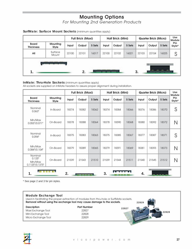
Mounting OptionsFor Mounting 2nd Generation Products
Module Exchange ToolUsed in facilitating the proper extraction of modules from thru-hole or SurfMate sockets.Removal without using the exchange tool may cause damage to the sockets.
Description Part NumberMaxi Exchange Tool 22827Mini Exchange Tool 22828Micro Exchange Tool 22829
Full Brick (Maxi) Half Brick (Mini) Quarter Brick (Micro)
Board Mounting Input Output 5 Sets Input Output 5 Sets Input Output 5 SetsThickness Style
In-Board 18374 18382 18362 18374 18384 18366 18376 18386 18370 S
On-Board 18378 18388 18364 18378 18390 18368 18380 18392 18372 N
In-Board 18375 18383 18363 18375 18385 18367 18377 18387 18371 S
On-Board 18379 18389 18365 18379 18391 18369 18381 18393 18373 N
On-Board 21539 21543 21510 21539 21544 21511 21540 21545 21512 N
Nominal0.063"
Min/Max0.055"/0.071"
Nominal 0.094"
Min/Max0.084"/0.104"
Nominal 0.125"
Min/Max0.1125"/0.1375"
InMate: Thru-Hole Sockets (minimum quantities apply)All sockets are supplied on InMate headers to assure proper alignment during installation.
22827
22829
22828
Full Brick (Maxi) Half Brick (Mini) Quarter Brick (Micro)
Board Mounting Input Output 5 Sets Input Output 5 Sets Input Output 5 SetsThickness Style
SurfaceAllMount
22100 22101 16017 22100 22102 16021 22103 22104 16025 S
1. 2. 3.
1. 2. 3. 4.
Use Module
PinStyle*
Use Module
PinStyle*
* See page 2 and 3 for pin styles.
SurfMate: Surface Mount Sockets (minimum quantities apply)

28 v i c o r p o w e r . c o m
StandoffsFor 2nd Generation Products
Board Mounting Slotted Thru-hole ThreadedThickness Options Baseplate Baseplate Baseplate
* Kits include six (6) standoffs and screws. Mini and Micro modules require a minimum of four (4) standoffs.Bags of one hundred (100) do not include screws; #4-40 thread hardware required.
Nom. Mounting Pin Thru-Hole Threaded Thru-Hole Threaded Thru-Hole(Min/Max) Style Style Heat Sink Heat Sink Heat Sink Heat Sink Heat Sink
Kit -18150 Kit -18151 Kit -18146 Kit -18147 Kit -18146
Bag-19126 Bag-19127 Bag-19122 Bag-19123 Bag-19122
Kit -18156 Kit -18157 Kit -18150 Kit -18152 Kit -18150
Bag-19132 Bag-19133 Bag-19126 Bag-19128 Bag-19126
Kit -18150 Kit -18151 Kit -18146 Kit -18147 Kit -18146
Bag-19126 Bag-19127 Bag-19122 Bag-19123 Bag-19122
Nominal0.063"
Min/Max0.055"/0.071"
Nominal 0.094"
Min/Max0.084"/0.104"
Nom. 0.125"Min/Max
0.113"/0.138"
In-Board
On-Board
In-Board
On-Board
On-Board
Standoff Kits for InMate Mounted Modules*
Standoff Kits for Solder Mounted Modules*
0.063"(0.055"/0.071")
0.094"(0.084"/0.104")
In-Board
On-Board
In-Board
Standard
L
L
Board Mounting Slotted Thru-hole ThreadedThickness Options Baseplate Baseplate Baseplate
Nom. Mounting Thru-Hole Threaded Thru-Hole Threaded Thru-Hole(Min/Max) Style Heat Sink Heat Sink Heat Sink Heat Sink Heat Sink
Kit -20178 Kit -20179 Kit -20176 Kit -20177 Kit -20176
Bag-20188 Bag-20189 Bag-20186 Bag-20187 Bag-20186
Standoff Kits for SurfMate Mounted Modules*
All Surface Mount
Slotted Thru-Hole ThreadedBaseplate Baseplate Baseplate
Board Mounting Thru-Hole Threaded Thru-Hole Threaded Thru-HoleThickness Style Heat Sink Heat Sink Heat Sink Heat Sink Heat Sink
Kit -18153 Kit -18154 Kit -18148 Kit -18149 Kit -18148
Bag -19129 Bag -19130 Bag -19124 Bag -19125 Bag -19124
Kit -18158 Kit -18159 Kit -18153 Kit -18155 Kit -18153
Bag -19134 Bag -19135 Bag -19129 Bag -19131 Bag -19129
Kit -18153 Kit -18154 Kit -18148 Kit -18149 Kit -18148
Bag -19129 Bag -19130 Bag -19124 Bag -19125 Bag -19124
Kit -18156 Kit -18157 Kit -18150 Kit -18152 Kit -18150
Bag -19132 Bag -19133 Bag -19126 Bag -19128 Bag -19126
Kit - 24054 Kit -18157 Kit -24056 Kit - 18152 Kit-24056
Bag -19132 Bag -19133 Bag -19126 Bag - 19128 Bag-19126
For soldering modules directly to printed circuit board refer to application note Soldering Methods and Procedureswhich is available at www.vicorpower.com/support/apps-info/apps-notes.htm

v i c o r p o w e r . c o m 29
Thermal HardwareHeat Sinks
Longitudinal FinsThreaded Thru-Hole
MAXI
0.4” Fin - 17483
0.9” Fin - 15975
MINI
0.4” Fin - 17485
0.9” Fin - 15989
MICRO
0.4” Fin - 16285
0.9” Fin - 15971
MAXI
0.4” Fin - 18038
0.9” Fin - 17443
MINI
0.4” Fin - 18039
0.9” Fin - 17537
MICRO
0.4” Fin - 18030
0.9” Fin - 17539
Transverse FinsThreaded Thru-Hole
MAXI
0.4” Fin - 17510
0.9” Fin - 15960
MINI
0.4” Fin - 16297
0.9” Fin - 15985
MICRO
0.4” Fin - 16299
0.9” Fin - 15987
MAXI
0.4” Fin - 18068
0.9” Fin - 17570
MINI
0.4” Fin - 18073
0.9” Fin - 17572
MICRO
0.4” Fin - 18074
0.9” Fin - 17574
30 v i c o r p o w e r . c o m
0
20
40
60
80
100
120
140
0 5 10 15 20 25 30 35 40 45 50 55 60 65 70 75 80 85 90 95
100
Ambient Temperature (deg C)
Ou
tpu
t P
ow
er (
Wat
ts)
Thermal Performance CurvesMICRO
0
5
10
15
20
25
30
35
40
45
50
0 5 10 15 20 25 30 35 40 45 50 55 60 65 70 75 80 85 90 95 100
Ambient Temperature (deg C)
Ou
tpu
t P
ow
er (
Wat
ts)
0
5
10
15
20
25
30
35
40
45
50
0 5 10 15 20 25 30 35 40 45 50 55 60 65 70 75 80 85 90 95 100
Ambient Temperature (deg C)
Ou
tpu
t P
ow
er (
Wat
ts)
0
5
10
15
20
25
30
35
40
45
50
0 5 10 15 20 25 30 35 40 45 50 55 60 65 70 75 80 85 90 95 100
Ambient Temperature (deg C)
Ou
tpu
t P
ow
er (
Wat
ts)
0
10
20
30
40
50
60
70
0 5 10 15 20 25 30 35 40 45 50 55 60 65 70 75 80 85 90 95 100
Ambient Temperature (deg C)
Ou
tpu
t P
ow
er (
Wat
ts)
0
10
20
30
40
50
60
700 5 10 15 20 25 30 35 40 45 50 55 60 65 70 75 80 85 90 95 100
Ambient Temperature (deg C)
Ou
tpu
t P
ower
(W
atts
)
0
10
20
30
40
50
60
70
0 5 10 15 20 25 30 35 40 45 50 55 60 65 70 75 80 85 90 95 100
Ambient Temperature (deg C)
Ou
tpu
t P
ower
(W
atts
)
0
10
20
30
40
50
60
70
80
90
100
0 5 10 15 20 25 30 35 40 45 50 55 60 65 70 75 80 85 90 95
100
Ambient Temperature (deg C)
Ou
tpu
t P
ow
er (
Wat
ts)
0
10
20
30
40
50
60
70
80
90
100
0 5 10 15 20 25 30 35 40 45 50 55 60 65 70 75 80 85 90 95 100
Ambient Temperature (deg C)
Ou
tpu
t P
ow
er (
Wat
ts)
0
10
20
30
40
50
60
70
80
90
100
0 5 10 15 20 25 30 35 40 45 50 55 60 65 70 75 80 85 90 95 100
Ambient Temperature (deg C)
Ou
tpu
t P
ow
er (
Wat
ts)
0
20
40
60
80
100
120
140
0 5 10 15 20 25 30 35 40 45 50 55 60 65 70 75 80 85 90 95
100
Ambient Temperature (deg C)
Ou
tpu
t P
ow
er (
Wat
ts)
0
20
40
60
80
100
120
140
0 5 10 15 20 25 30 35 40 45 50 55 60 65 70 75 80 85 90 95
100
Ambient Temperature (deg C)
Ou
tpu
t P
ow
er (
Wat
ts)
Slotted Baseplate 0.4'' Heat Sink 0.9'' Heat Sink
2V (1.8)
3.3V(2.5)
5V
12-48V
θbm = 0.15°C/W Baseplate 0.9'' Longitudinal Fins 0.9'' Transverse Fins 0.4'' Longitudinal Fins 0.4'' Transverse Fins
Free Air 10.90 5.37 5.04 7.77 7.76
200 LFM 6.90 2.51 2.31 3.87 3.58
400 LFM 4.78 1.79 1.68 2.68 2.52
600 LFM 3.74 1.42 1.31 2.13 2.01
800 LFM 3.15 1.20 1.10 1.78 1.67
1000 LFM 2.79 1.06 0.97 1.48 1.45
1200 LFM 2.49 0.93 0.88 1.32 1.29
Free Air 200 LFM 400 LFM 600 LFM
800 LFM 1000 LFM 1200 LFM

v i c o r p o w e r . c o m 31
Thermal Performance CurvesMINI
0
10
20
30
40
50
60
70
80
90
1000 5 10 15 20 25 30 35 40 45 50 55 60 65 70 75 80 85 90 95 100
Ambient Temperature (deg C)
Ou
tpu
t P
ower
(W
atts
)
0
10
20
30
40
50
60
70
80
90
100
0 5 10 15 20 25 30 35 40 45 50 55 60 65 70 75 80 85 90 95 100
Ambient Temperature (deg C)
Ou
tpu
t P
ow
er (
Wat
ts)
0
10
20
30
40
50
60
70
80
90
100
0 5 10 15 20 25 30 35 40 45 50 55 60 65 70 75 80 85 90 95 100
Ambient Temperature (deg C)
Ou
tpu
t P
ow
er (
Wat
ts)
0
20
40
60
80
100
120
140
0 5 10 15 20 25 30 35 40 45 50 55 60 65 70 75 80 85 90 95 100
Ambient Temperature (deg C)
Ou
tpu
t P
ow
er (
Wat
ts)
0
20
40
60
80
100
120
140
0 5 10 15 20 25 30 35 40 45 50 55 60 65 70 75 80 85 90 95 100
Ambient Temperature (deg C)
Ou
tpu
t P
ow
er (
Wat
ts)
0
20
40
60
80
100
120
140
0 5 10 15 20 25 30 35 40 45 50 55 60 65 70 75 80 85 90 95 100
Ambient Temperature (deg C)
Ou
tpu
t P
ow
er (
Wat
ts)
0
20
40
60
80
100
120
140
160
180
200
0 5 10 15 20 25 30 35 40 45 50 55 60 65 70 75 80 85 90 95 100
Ambient Temperature (deg C)
Ou
tpu
t P
ow
er (
Wat
ts)
0
20
40
60
80
100
120
140
160
180
200
0 5 10 15 20 25 30 35 40 45 50 55 60 65 70 75 80 85 90 95 100
Ambient Temperature (deg C)
Ou
tpu
t P
ow
er (
Wat
ts)
0
20
40
60
80
100
120
140
160
180
200
0 5 10 15 20 25 30 35 40 45 50 55 60 65 70 75 80 85 90 95 100
Ambient Temperature (deg C)
Ou
tpu
t P
ow
er (
Wat
ts)
0
50
100
150
200
250
300
0 5 10 15 20 25 30 35 40 45 50 55 60 65 70 75 80 85 90 95 100
Ambient Temperature (deg C)
Ou
tpu
t P
ow
er (
Wat
ts)
0
50
100
150
200
250
300
0 5 10 15 20 25 30 35 40 45 50 55 60 65 70 75 80 85 90 95 100
Ambient Temperature (deg C)
Ou
tpu
t P
ow
er (
Wat
ts)
0
50
100
150
200
250
300
0 5 10 15 20 25 30 35 40 45 50 55 60 65 70 75 80 85 90 95 100
Ambient Temperature (deg C)
Ou
tpu
t P
ow
er (
Wat
ts)
Slotted Baseplate 0.4'' Heat Sink 0.9'' Heat Sink
2V (1.8)
3.3V(2.5)
5V
12-48V
θbm = 0.15°C/W Baseplate 0.9'' Longitudinal Fins 0.9'' Transverse Fins 0.4'' Longitudinal Fins 0.4'' Transverse Fins
Free Air 7.94 4.10 3.93 6.28 6.34
200 LFM 4.50 1.72 1.93 2.81 3.00
400 LFM 3.20 1.26 1.38 1.98 2.09
600 LFM 2.52 1.02 1.06 1.55 1.59
800 LFM 2.15 0.86 0.89 1.24 1.31
1000 LFM 1.89 0.75 0.77 1.05 1.11
1200 LFM 1.69 0.68 0.70 0.94 0.99
Free Air 200 LFM 400 LFM 600 LFM
800 LFM 1000 LFM 1200 LFM

32 v i c o r p o w e r . c o m
Thermal Performance CurvesMAXI
0
20
40
60
80
100
120
140
160
0 5 10 15 20 25 30 35 40 45 50 55 60 65 70 75 80 85 90 95 100
Ambient Temperature (deg C)
Ou
tpu
t P
ow
er (
Wat
ts)
0
20
40
60
80
100
120
140
160
0 5 10 15 20 25 30 35 40 45 50 55 60 65 70 75 80 85 90 95 100
Ambient Temperature (deg C)
Out
put P
ower
(Wat
ts)
0
20
40
60
80
100
120
140
160
0 5 10 15 20 25 30 35 40 45 50 55 60 65 70 75 80 85 90 95 100
Ambient Temperature (deg C)
Out
put P
ower
(Wat
ts)
0
50
100
150
200
250
0 5 10 15 20 25 30 35 40 45 50 55 60 65 70 75 80 85 90 95 100
Ambient Temperature (deg C)
Ou
tpu
t P
ow
er (
Wat
ts)
0
50
100
150
200
2500 5 10 15 20 25 30 35 40 45 50 55 60 65 70 75 80 85 90 95 100
Ambient Temperature (deg C)
Ou
tpu
t P
ow
er (
Wat
ts)
0
50
100
150
200
250
0 5 10 15 20 25 30 35 40 45 50 55 60 65 70 75 80 85 90 95 100
Ambient Temperature (deg C)
Ou
tpu
t P
ow
er (
Wat
ts)
0
50
100
150
200
250
300
350
400
0 5 10 15 20 25 30 35 40 45 50 55 60 65 70 75 80 85 90 95 100
Ambient Temperature (deg C)
Ou
tpu
t P
ow
er (
Wat
ts)
0
50
100
150
200
250
300
350
400
0 5 10 15 20 25 30 35 40 45 50 55 60 65 70 75 80 85 90 95 100
Ambient Temperature (deg C)
Ou
tpu
t P
ow
er (
Wat
ts)
0
50
100
150
200
250
300
350
400
0 5 10 15 20 25 30 35 40 45 50 55 60 65 70 75 80 85 90 95 100
Ambient Temperature (deg C)
Ou
tpu
t P
ow
er (
Wat
ts)
0
100
200
300
400
500
600
0 5 10 15 20 25 30 35 40 45 50 55 60 65 70 75 80 85 90 95
100
Ambient Temperature (deg C)
Ou
tpu
t P
ow
er
(Wa
tts
)
0
100
200
300
400
500
600
0 5 10 15 20 25 30 35 40 45 50 55 60 65 70 75 80 85 90 95 100
Ambient Temperature (deg C)
Po
wer
Ou
tpu
t (W
atts
)
0
100
200
300
400
500
600
0 5 10 15 20 25 30 35 40 45 50 55 60 65 70 75 80 85 90 95 100
Ambient Temperature (deg C)
Po
wer
Ou
tpu
t (W
atts
)
Slotted Baseplate 0.4'' Heat Sink 0.9'' Heat Sink
2V (1.8)
3.3V(2.5)
5V
12-48V
θbm = 0.15°C/W Baseplate 0.9'' Longitudinal Fins 0.9'' Transverse Fins 0.4'' Longitudinal Fins 0.4'' Transverse Fins
Free Air 4.98 2.89 2.24 3.72 3.49
200 LFM 3.23 1.30 1.02 2.14 1.53
400 LFM 2.17 0.90 0.72 1.48 1.08
600 LFM 1.73 0.72 0.60 1.10 0.87
800 LFM 1.46 0.59 0.51 0.86 0.70
1000 LFM 1.27 0.51 0.44 0.71 0.60
1200 LFM 1.14 0.46 0.41 0.61 0.55
Free Air 200 LFM 400 LFM 600 LFM
800 LFM 1000 LFM 1200 LFM

v i c o r p o w e r . c o m 33
Mechanical DrawingsMICRO
567
4321
(REF)
0.0802,03
DIA. (7X)
0.215,2
0.27
6,9(2X)
1.0426,4
1.4536,8
0.275
6,99
0.80020,32
0.52513,34
0.40010,16
0.12*
3,1
0.20**
5,08
FULL R (6X)
0.102,5
CHAMFER
(REF.)
(6X)
0.6516,5
0.4912,4
1.3033,0
2.2857,9
1.4536,8
0.133,3
0.06
1,5R (3X)
0.01
X 45˚
Use a4-40 Screw (6x)
Torque to:5 in-lbs
0.57 N-m
0.5413,7
0.4310,9
Pin Style 2&N(Long Pin)
0.6215,7
Pin Style 1&S(Short Pin)
(7X)
(7X)
Slotted (Style 1)
or
Threaded (Style 2) 4-40 UNC-2B (6X)
or
Thru Hole (Style 3) #30 Drill Thru (6X)(0.1285)
(ALL M
AR
KIN
GS
TH
IS S
UR
FAC
E)
ALUMINUM BASEPLATE
12,7 ±0,5
0.50 ±0.02
* Style 1 baseplate only ** Style 2 & 3 baseplates *** Reserved for Vicor accessories Not for mounting
style 2 & 3 baseplates only(4X)***
0.490 ±.015
12,45 ±0,38(REF)
2.00050,80
0.235±.0155,97±0,38
(REF)
0.350±.0158,89±0,38
(REF)
1.2732,3
0.092,3
2 3
6
1
7
4
5
PLATEDTHRU HOLE
DIA
±0,08*DENOTES TOL = ±0.003
0.1333,38
1.734**44,04
.400*10,16
1.140**
28,96
0.170*4,32
0.800*
20,32
0.525*13,34
0.275*6,99
2.000*
50,80
0.061,5
R (4X)
INBOARDSOLDERMOUNT
PIN STYLE 1&S0.094 ±0.003 2,39 ±0,08
0.4310,9
(7X)
**PCB WINDOW
PCB THICKNESS0.062 ±0.0101,57 ±0,25
0.5313,5
ONBOARDSOLDERMOUNT
PIN STYLE 2&N0.094 ±0.003 2,39 ±0,08
PINS STYLES STYLE 1 & 2: TIN/LEADHOT SOLDER DIPPEDSTYLE S & N: GOLD PLATED COPPER
ALUMINUMBASEPLATE
ALL MARKINGSTHIS SURFACE
PCB Mounting Specifications
Converter PinsNo. Function Label
1 +In +
2Primary
PCControl
3 Parallel PR
4 –In –
5 –Out –
6Secondary
SCControl
7 +Out +
For soldering modules directly to printed circuit board refer to application note Soldering Methods and Procedureswhich is available at www.vicorpower.com/support/apps-info/apps-notes.htm
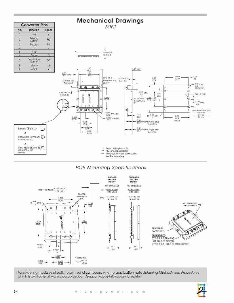
34 v i c o r p o w e r . c o m
Mechanical DrawingsMINI
PCB Mounting Specifications
ALL MARKINGSTHIS SURFACE
PINS STYLES STYLE 1 & 2: TIN/LEADHOT SOLDER DIPPEDSTYLE S & N: GOLD PLATED COPPER
ALUMINUMBASEPLATE
0.1954,95
1.400*35,56
1.000*25,40
0.700*17,78
0.400*10,16
1.79045,470.06
1,5R (4X) 0.158
4,01
56789
1 2 3 4
±0.003±0,08
* DENOTES
TOL =
PCB THICKNESS0.062 ±0.010
1,57 ±0,25
PIN STYLE 1&S
0.094 ±0.0032,39 ±0,08
INBOARDSOLDERMOUNT
0.4310,9
0.5313,5
1.900*48.261.900*48,26
1.584*40,23
0.164 ±0.0034,16 ±0,08
PIN STYLE 2&N
0.094 ±0.0032,39 ±0,08
ONBOARDSOLDERMOUNT
0.164 ±0.0034,16 ±0,08
PLATEDTHRU HOLE
DIA
(7X)
(2X)
(2X)
0.01
0.358,8
0.20**5,1
0.12*3,1
DIA,(7X)
0.1503,81
(REF)
DIA,(2X)
0.0802,03
431
9 8
2
7 6 5
0.235,8
0.40010,16
1.40035,56
1.00025,40
0.70017,78
2.2055,91.7444,2
FULL R (6X)
(6X)
(REF.)
0.102,5
1.3033,0
2.2857,9
2.2055,9
0.130
3,30
0.4912,4
0.6516,5
0.061,5
R (3X)
X 45˚
CHAMFER
Use a 4-40 Screw (6X)Torque to:
5 in-lbs.57 N-m
0.5413,7
0.4310,9
Pin Style 2&N(Long Pin)
0.6215,7
Pin Style 1&S(Short Pin)
(9X)
(9X)Slotted (Style 1)
or
Threaded (Style 2) 4-40 UNC-2B (6X)
or
Thru Hole (Style 3) #30 Drill Thru (6X)(0.1285)
(ALL M
AR
KIN
GS
T
HIS
SU
RFA
CE
)
ALUMINUM BASEPLATE
0.50 ±0.0212,7 ±0,5
* Style 1 baseplate only ** Style 2 & 3 baseplates *** Reserved for Vicor accessories Not for mounting
style 2 & 3 baseplates only(4X)***
0.300 ±0.0157,62 ±0,38
0.300 ±0.0157,62 ±0,38
1.90048,26
2.00050,80
0.102,5
Converter PinsNo. Function Label
1 +In +
2 Primary PCControl3 Parallel PR4 -In -5 -Out -6 -Sense -S
7 Secondary SCControl8 +Sense +S9 +Out +
For soldering modules directly to printed circuit board refer to application note Soldering Methods and Procedureswhich is available at www.vicorpower.com/support/apps-info/apps-notes.htm
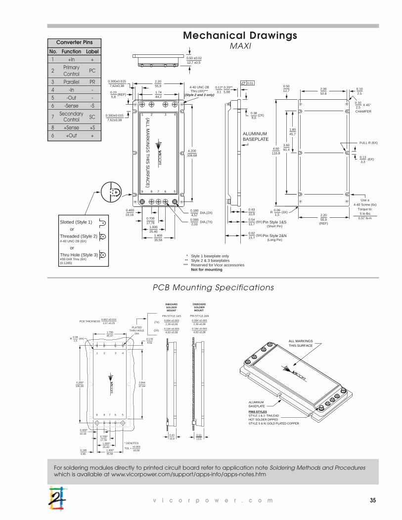
v i c o r p o w e r . c o m 35
Mechanical DrawingsMAXI
PCB Mounting Specifications
1.7444,2
2.2055,9
56789
4321
0.235,8
(REF)
0.1804,57
0.0802,03
1.40035,56
1.00025,40
0.70017,78
0.40010,16
DIA,(7X)
DIA,(2X)
4-40 UNC-2BThru (4X)***
(Style 2 and 3 only)
Slotted (Style 1)
or
Threaded (Style 2) 4-40 UNC-2B (6X)
or
Thru Hole (Style 3) #30 Drill Thru (6X)(0.1285)
0.5012,7
0.061,5 2.20
55,9(REF)
1.8045,7
4.60116,8
3.6091,4
0.133,3
FULL R (6X)
(6X)
R (3X)
CHAMFER
0.102,5
X 45°
0.5413,7
0.4310,9
0.389,6
0.20**5,08
0.12*3,1
(2X)
0.01
Use a4-40 Screw (6x)
Torque to:5 in-lbs
0.57 N-m
Pin Style 2&N(Long Pin)
0.6215,7
Pin Style 1&S(Short Pin)
(9X)
(9X)
(ALL M
AR
KIN
GS
TH
IS S
UR
FAC
E)
ALUMINUM BASEPLATE
0.50 ±0.0212,7 ±0,5
* Style 1 baseplate only ** Style 2 & 3 baseplates *** Reserved for Vicor accessories Not for mounting
4.200106,68
0.300±0.0157,62±0,38
0.300±0.0157,62±0,38
2.0050,8
0.102,5
ALL MARKINGSTHIS SURFACE
PINS STYLES STYLE 1 & 2: TIN/LEADHOT SOLDER DIPPEDSTYLE S & N: GOLD PLATED COPPER
ALUMINUMBASEPLATE
0.1954,95
1.400*35,56
1.000*25,40
0.700*17,78
0.400*10,16
3.84497,64
4.200*106,68
1.79045,470.06
1,5R (4X) 0.178
4,52
56789
1 2 3 4
±0.003±0,08
* DENOTES
TOL =
PLATEDTHRU HOLE
DIA
PCB THICKNESS0.062 ±0.010
1,57 ±0,25
PIN STYLE 1&S
0.094 ±0.0032,39 ±0,08
0.194 ±0.0034,93 ±0,08
PIN STYLE 2&N
0.094 ±0.0032,39 ±0,08
0.194 ±0.0034,93 ±0,08
INBOARDSOLDERMOUNT
0.4310,9
ONBOARDSOLDERMOUNT
(7X)
(2X)
0.5313,5
Converter Pins
No. Function Label1 +In +
2Primary
PCControl
3 Parallel PR
4 -In -
5 -Out -
6 -Sense -S
7Secondary
SCControl
8 +Sense +S
6 +Out +
For soldering modules directly to printed circuit board refer to application note Soldering Methods and Procedureswhich is available at www.vicorpower.com/support/apps-info/apps-notes.htm

36 v i c o r p o w e r . c o m
Notes Page

v i c o r p o w e r . c o m 37
Vicor Technical Support
Vicor’s technical support team is staffed withapplications engineers to provide the product andapplication information and technical assistancecustomers need concerning Vicor products andpower solutions. Our facilities house electronicslaboratories where Vicor applications engineers canevaluate specific customer design issues and offer awide range of component-based power solutionsthat include distributed power, current sharing, N + 1redundancy, thermal management, and compliancewith safety and performance standards.
Applications engineers ...
• Answer technical questions (by phone, fax, email,or the Vicor web site)
• Assist with component-based power system design.• Support user needs through visits to Vicor and
customer facilities
• Help select the most appropriate product for your application
If you have a specific technical question, just call oremail an applications engineer located at any of ouroffices around the globe.
USAVicor Corporation (Corporate Headquarters)25 Frontage RoadAndover, MA 01810-5413
For General InfoTel: 978-470-2900In U.S. and Canada: 800-735-6200Fax: 978-475-6715
For Technical Support Tel: 800-927-9474Fax: 978-749-3341E-mail: [email protected]
For Sales Support (Vicor Express)In U.S. and Canada: 800-735-6200Fax: 978-475-6715E-mail: [email protected]
Vicor Corporation 377 E. Butterfield RoadLombard, IL 60148Tel: 630-769-8780Fax: 630-769-8782
Vicor Westcor Corporation 560 Oakmead ParkwaySunnyvale, CA 94086-4049Tel: 408-522-5280Fax: 408-774-5555
Picor CorporationP.O. Box 859Slatersville, RI 02876Tel: 401-235-1100Fax: 401-235-1117
EuropeVicor France6, Parc ArianeBâtiment "Le Mercure"78284 Guyancourt CedexFranceTel: +33-1-3452-18300800 419 419 (in France)Fax: +33-1-3452-2830E-mail: [email protected]
Vicor GermanyAdalperostraße 2985737 Ismaning, GermanyTel: +49-89-962439-00800 018 29 18 (in Germany)Fax: +49-89-962439-39E-mail: [email protected]
Vicor ItalyVia Milanese, 2020099 Sesto S. GiovanniMilano, ItalyTel: +39-02-2247-2326800 899 677 (in Italy)Fax: +39-02-2247-3166E-mail: [email protected]
Vicor U.K.Coliseum Business CentreRiverside Way, CamberleySurrey GU15 3YLEnglandTel: +44-1276-678-222
In UK: 0800-980-8427In Denmark: 80 88 11 41In Norway: 800 11083In Sweden: 020 798236
Fax: +44-1276-681-269E-mail: [email protected]
Asia-PacificVicor Japan Co., Ltd.6F, POLA 3rd Bldg.8-9-5, Nishi-gotanda Shinagawa-kuTokyo 141 Japan Tel: +81-3-5487-3880Fax: +81-3-5487-3885www.vicr.co.jp
Vicor Hong Kong Rm 511, Tower 1, Silvercord30 Canton RoadTsim Sha TsuiHong Kongwww.vicr.com.cnTel: +852-2956-1782Fax: +852-2956-0782
In Latin America: Call the number below and ask the operator to connect you to 800-735-6200.Argentina: 001-800-200-1111Brazil: 000+8010Mexico: 95-800-462-4240
Information furnished by Vicor is believed to be accurate and reliable. However, no responsibility is assumed by Vicorfor its use. No license is granted by implication or otherwise under any patent or patent rights of Vicor. Vicorcomponents are not designed to be used in applications, such as life support systems, wherein a failure ormalfunction could result in injury or death. All sales are subject to Vicor’s Terms and Conditions of Sale, which areavailable upon request. Specifications are subject to change without notice.

2 5 F r o n t a g e R o a d
A n d ov e r, M A 0 1 8 1 0
v i c o r p o w e r . c o m
P/N 25722 Rev 3 10/02/10M