3-Wire Serial EEPROM
10
3-Wire Serial EEPROM 1K, 2K and 4Kbit (8-bit or 16-bit wide) FEATURES Standard Voltage and Low Voltage Operation: HG93C46/56/66: V CC = 2.5V to 5.5V HG93C46A/56A/66A: V CC = 1.8V to 5.5V User Selectable Internal Organization: HG93C46: 128 x 8 or 64 x 16 HG93C56: 256 x 8 or 128 x 16 HG93C66: 512 x 8 or 256 x 16 2 MHz Clock Rate (5V) Compatibility. Industry Standard 3-wire Serial Interface. Self-Timed ERASE/WRITE Cycles (5ms max including auto-erase). Automatic ERAL before WRAL. Sequential READ Function. High Reliability: Typical 1 Million Erase/Write Cycle Endurance. 100 Years Data Retention. Industrial Temperature Range (-40 o C to 85 o C). Standard 8-pin DIP/SOP/TSSOP/DFN Pb-free Packages. DESCRIPTION The HG93C46/56/66 series are 1024/2048/4096 bits of serial Electrical Erasable and Programmable Read Only Memory, commonly known as EEPROM. They are organized as 64/128/256 words of 16 bits each when the ORG pin is connected to VCC (or unconnected) and 128/256/512 words of 8 bits (1 byte) each when the ORG pin is tied to ground. The devices are fabricated with proprietary advanced CMOS process for low power and low voltage applications. These devices are available in standard 8-lead DIP, 8-lead JEDEC SOP, 8-lead TSSOP and 8-lead DFN packages. Our extended V CC range (1.8V to 5.5V) devices enables wide spectrum of applications. The HG93C46/56/66 is enabled through the Chip Select pin (CS), and accessed via a 3-wire serial interface consisting of Data Input (DI), Data Output (DO), and Shift Clock (SCL). Upon receiving a READ instruction at DI, the address is decoded and the data is clocked out serially on the data output pin DO. The WRITE cycle is completely self-timed and no separate ERASE cycle is required before WRITE. The WRITE cycle is only enabled when the part is in the ERASE/WRITE ENABLE state. Once a device begins its self-timed program procedure, the data out pin (DO) can indicate the READY/BUSY status by rising chip select (CS). 93C46/56/66 1 2018 AUG http://www.hgsemi.com.cn
Transcript of 3-Wire Serial EEPROM

3-Wire Serial EEPROM 1K, 2K and 4Kbit (8-bit or 16-bit wide)
FEATURES
Standard Voltage and Low Voltage Operation:
HG93C46/56/66: V CC = 2.5V to 5.5V
HG93C46A/56A/66A: V CC = 1.8V to 5.5V
User Selectable Internal Organization:
HG93C46: 128 x 8 or 64 x 16
HG93C56: 256 x 8 or 128 x 16
HG93C66: 512 x 8 or 256 x 16
2 MHz Clock Rate (5V) Compatibility.
Industry Standard 3-wire Serial Interface.
Self-Timed ERASE/WRITE Cycles (5ms max including auto-erase).
Automatic ERAL before WRAL.
Sequential READ Function.
High Reliability: Typical 1 Million Erase/Write Cycle Endurance.
100 Years Data Retention.
Industrial Temperature Range (-40o C to 85o C).
Standard 8-pin DIP/SOP/TSSOP/DFN Pb-free Packages.
DESCRIPTION
The HG93C46/56/66 series are 1024/2048/4096 bits of serial Electrical Erasable and Programmable
Read Only Memory, commonly known as EEPROM. They are organized as 64/128/256 words of 16 bits
each when the ORG pin is connected to VCC (or unconnected) and 128/256/512 words of 8 bits (1 byte)
each when the ORG pin is tied to ground. The devices are fabricated with proprietary advanced CMOS
process for low power and low voltage applications. These devices are available in standard 8-lead DIP,
8-lead JEDEC SOP, 8-lead TSSOP and 8-lead DFN packages. Our extended VCC range (1.8V to 5.5V)
devices enables wide spectrum of applications.
The HG93C46/56/66 is enabled through the Chip Select pin (CS), and accessed via a 3-wire serial
interface consisting of Data Input (DI), Data Output (DO), and Shift Clock (SCL). Upon receiving a READ
instruction at DI, the address is decoded and the data is clocked out serially on the data output pin DO.
The WRITE cycle is completely self-timed and no separate ERASE cycle is required before WRITE. The
WRITE cycle is only enabled when the part is in the ERASE/WRITE ENABLE state. Once a device
begins its self-timed program procedure, the data out pin (DO) can indicate the READY/BUSY status by
rising chip select (CS).
93C46/56/66
1 2018 AUGhttp://www.hgsemi.com.cn

PIN CONFIGURATION
All these packaging types come in Pb-free certified.
VCC
DCORG
GND
DISCL
CS
DO
1
2
3
4
8
7
6
5
8L DIP8L SOP8L TSSOP8L DFN
ORG
GND
DO
DI
CS
VCC
DC
SCL
1
2
3
4
8
7
6
5
8L SOPRotated (R)
93C46 only
ABSOLUTE MAXIMUM RATINGS
Industrial operating temperature: -40oC to 85oC
Storage temperature: -50oC to 125oC
Input voltage on any pin relative to ground: -0.3V to VCC + 0.3V
Maximum voltage: 8V
* Stresses exceed those listed under “Absolute Maximum Rating” may cause permanent damage to the device. Functional operation of the device at conditions beyond those listed in the specification is not guaranteed. Prolonged exposure to extreme conditions may affect device reliability or functionality.
Pin Name Pin Function
CS Chip Select
SCL Serial Clock
DI Serial Data Input
DO Serial Data Output
ORG Internal Organization
DC Don’t Connect
VCC Power Supply
GND Ground
93C46/56/66
2 2018 AUGhttp://www.hgsemi.com.cn

PIN DESCRIPTIONS
(A) SERIAL CLOCK (SCL)
The rising edge of this SCL input is to latch data into the EEPROM device while the rising edge of this clock is to clock data out of the EEPROM device.
(B) CHIP SELECT (CS)
This is the chip select input signal for the serial EEPROM device. .
(C) SERIAL DATA INPUT (DI)
This is data input signal for the serial device.
(D) SERIAL DATA OUTPUT (DO)
This is data output signal for the serial device.
(E) INTERNAL ORGANIZATION (ORG)
This is internal organization input signal for the serial EEPROM device. When the ORG pin is connected to VCC or unconnected the EEPROM is organized as 64/128/256 word of 16 bits each and when ORG pin is connected to ground the EEPROM is organized as 128/256/512 byte of 8 bits each. Typically, these signals are hardwired to either VIH or VIL. If left unconnected, they are internally recognized as VIH.
93C46/56/66
3 2018 AUGhttp://www.hgsemi.com.cn

MEMORY ORGANIZATION The HG93C46/56/66 memory is organized either as bytes (x8) or as words (x16). If Internal Organization (ORG) is unconnected (or connected to VCC) the words (x16) organization is selected; When Internal Organization is connected to ground the bytes (x8) organization is selected.
INSTRUCTION SET for the HG93C46
Address Data Instruction SB
Op Code x 8 x 16 x 8 x 16
Comments
READ 1 10 A6 - A0 A5 - A0 Reads data stored in memory, at specified address.
EWEN 1 00 11xxxxx 11xxxx Write enable must precede all programming modes.
EWDS 1 00 00xxxxx 00xxxx Disables all programming instructions.
ERASE 1 11 A6 - A0 A5 - A0 Erase memory location An - A0. WRITE 1 01 A6 - A0 A5 - A0 D7 - D0 D15 - D0 Writes memory location An - A0.ERAL 1 00 10xxxxx 10xxxx Erases all memory locations. WRAL 1 00 01xxxxx 01xxxx D7 - D0 D15 - D0 Writes all memory locations.
INSTRUCTION SET for the HG93C56 and HG93C66
Address Data Instruction SB
Op Code x 8 x 16 x 8 x 16
Comments
READ 1 10 A8- A0 A7- A0 Reads data stored in memory, at specified address.
EWEN 1 00 11xxxxxxx 11xxxxxx Write enable must precede all programming modes.
EWDS 1 00 00xxxxxxx 00xxxxxx Disables all programming instructions.
ERASE 1 11 A8- A0 A7- A0 Erase memory location An - A0. WRITE 1 01 A8- A0 A7- A0 D7 - D0 D15 - D0 Writes memory location An - A0.ERAL 1 00 10xxxxxxx 10xxxxxx Erases all memory locations. WRAL 1 00 01xxxxxxx 01xxxxxx D7 - D0 D15 - D0 Writes all memory locations.
.
(A) START BIT (SB) Each instruction is preceded by a rising edge on Chip Select (CS) with Serial Clock (SCL) being held Low.
(B) OPERATION CODE (OP-CODE) Two op-code bits, read on Serial Data Input (DI) during the rising edge of Serial Clock (SCL).
(C) ADDRESS The address bits of the byte or word that is to be accessed. For the HG93C46, the address is made up of 6 bits for the x16 organization or 7 bits for x8 organization. For the HG93C56, the address is made up of 7 bits for the x16 organization or 8 bits for x8 organization. For the HG93C66, the address is made up of 8 bits for the x16 organization or 9 bits for x8 organization.
(D) DATA The data bits of the byte or word that is to be accessed. For the HG93C46/56/66, the data is made up of 16 bits (word) for the x16 organization or 8 bits (byte) for x8 organization.
93C46/56/66
4 2018 AUGhttp://www.hgsemi.com.cn
INSTRUCTION SETS DESCRIPTION
(A) READ
The Read (READ) instruction contains the Address code for the memory location to be read. After the instruction and address are decoded, data from the selected memory location is available at the serial output pin DO. Output data changes are synchronized with the rising edges of serial clock SK. It should be noted that when a dummy bit (logic “0”) precedes the 8- or 16-bit data output string.
(B) ERASE/WRITE ENABLE
To assure data integrity, the part automatically goes into the Erase/Write Disable (EWDS) state when power is first applied. An Erase/Write Enable (EWEN) instruction must be executed first before any programming instructions can be carried out. Please note that once in the Erase/Write Enable state, programming remains enabled until an Erase/Write Disable (EWDS) instruction is executed or VCC power is removed from the part.
(C) ERASE/WRITE DISABLE
To protect against accidental data disturb, the Erase/Write Disable (EWDS) instruction disables all programming modes and should be executed after all programming operations. The operation of the READ instruction is independent of both the EWEN and EWDS instructions and can be executed at any time.
(D) ERASE
The Erase (ERASE) instruction programs all bits in the specified memory location to the logical “1” state. The self-timed erase cycle starts once the ERASE instruction and address are decoded. The DO pin outputs the READY/BUSY status of the part if CS is brought high after being kept low for a minimum of 250 ns (t
CS). A logic “1” at pin DO indicates that the selected memory location has been
erased, and the part is ready for another instruction.
(E) WRITE
The Write (WRITE) instruction contains the 8 or 16 bits of data to be written into the specified memory location. The self-timed programming cycle, t
WP, starts after the last bit of data is received at serial
data input pin DI. The DO pin outputs the READY/BUSY status of the part if CS is brought high after being kept low for a minimum of 250 ns (t
CS). A logic “0” at DO indicates that programming is still in
progress. A logic “1” indicates that the memory location at the specified address has been written with the data pattern contained in the instruction and the part is ready for further instructions. A READY/BUSY status cannot be obtained if the CS is brought high after the end of the self-timed programming cycle, t
WP.
(F) ERASE ALL
The Erase All (ERAL) instruction programs every bit in the memory array to the logic “1” state and is primarily used for testing purposes. The DO pin outputs the READY/BUSY status of the part if CS is brought high after being kept low for a minimum of 250 ns (t
CS). The ERAL instruction is valid only at
VCC
= 5.0V ± 10%.
(G) WRITE ALL
The Write All (WRAL) instruction programs all memory locations with the data patterns specified in the instruction. The DO pin outputs the READY/BUSY status of the part if CS is brought high after being kept low for a minimum of 250 ns (t
CS). The WRAL instruction is valid only at VCC = 5.0V ± 10%.
93C46/56/66
5 2018 AUGhttp://www.hgsemi.com.cn

Timing Diagrams
CS
SCL
DI
D O
A n A n+1 A1 A0
D n D n+1 D 1 D 0
STARTBIT
O PCO DE
ADDRDATA O UT
R E A D T im ing
CS
SCL
DI x x
STARTBIT
OPCODE
COMMAND
EWDS Timing
CS
SCL
DI x x
STARTBIT
OPCODE
COMMAND
EWEN Timing
93C46/56/66
6 2018 AUGhttp://www.hgsemi.com.cn

CS
SCL
DI
D O
A n An+1 A 1 A0
STARTB IT
OPCODE ADDR Twc
E R A SE T im ing
CS
SCL
DI
DO
An An+1 A1 A0
STARTBIT
OPCODE
ADDR DATA IN
WRITE Timing
Dn Dn+1 D1 D0
Twc
CS
SCL
DI
DO
x x
STARTBIT
OPCODE
ADDR Twc
ERAL Timing (1)
93C46/56/66
7 2018 AUGhttp://www.hgsemi.com.cn

CS
SCL
DI
DO
x x
STARTBIT
OPCODE
ADDR DATA IN
WRAL Timing (2)
Dn Dn+1 D1 D0
Twc
Note : 1. Valid only at VCC=4.5V to 5.5V 2. Valid only at VCC=4.5V to 5.5V
Synchronous Data Timing
t CSS t SCLH t SCLL t CSH
t DIHt DIS
t PD1t PD0 t DF
t SV t DF
IH
IL
V
V
IH
IL
V
V
IH
IL
V
V
IH
IL
V
V
IH
IL
V
VSTATUS VALID
CS
SCL
DI
DO ( read )
DO ( program )
93C46/56/66
8 2018 AUGhttp://www.hgsemi.com.cn

AC CHARACTERISTICS Applicable over recommended operating range from: T
AI = -40°C to +85°C, V
CC = +1.8V to +5.5V, T
AC = 0°C
to +70°C, VCC
= +1.8V to +5.5V (unless otherwise noted).
Symbol Parameter Test Condition Min Typ Max Units
fSCL SCL Clock Frequency
4.5V ≤ VCC
≤ 5.5V
2.7V ≤ VCC
≤ 5.5V
1.8V ≤ VCC
≤ 5.5V
0 0 0
2 1
0.25MHz
tSCLH SCL High Time
4.5V ≤ VCC
≤ 5.5V
2.7V ≤ VCC
≤ 5.5V1.8V ≤ V
CC ≤ 5.5V
250 250 1000
ns
tSCLL SCL Low Time
4.5V ≤ VCC
≤ 5.5V 2.7V ≤ V
CC ≤ 5.5V
1.8V ≤ VCC
≤ 5.5V
250 250 1000
ns
tCS Minimum CS Low Time
4.5V ≤ VCC
≤ 5.5V
2.7V ≤ VCC
≤ 5.5V
1.8V ≤ VCC
≤ 5.5V
250 250 1000
ns
tCSS CS Setup Time Relative to SCL
4.5V ≤ VCC
≤ 5.5V
2.7V ≤ VCC
≤ 5.5V
1.8V ≤ VCC
≤ 5.5V
50 50
200 ns
tDIS DI Setup Time Relative to SCL
4.5V ≤ VCC
≤ 5.5V
2.7V ≤ VCC
≤ 5.5V 1.8V ≤ V
CC ≤ 5.5V
100 100 400
ns
tCSH CS Hold Time Relative to SCL 0 ns
tDIH DI Hold Time Relative to SCL
4.5V ≤ VCC
≤ 5.5V
2.7V ≤ VCC
≤ 5.5V
1.8V ≤ VCC
≤ 5.5V
100 100 400
ns
tPD1 Output Delay to ‘1’ AC Test
4.5V ≤ VCC
≤ 5.5V
2.7V ≤ VCC
≤ 5.5V 1.8V ≤ V
CC ≤ 5.5V
250 250 1000
ns
tPD0 Output Delay to ‘0’ AC Test
4.5V ≤ VCC
≤ 5.5V 2.7V ≤ V
CC ≤ 5.5V
1.8V ≤ VCC
≤ 5.5V
250 250 1000
ns
tSV CS to Status Valid AC Test
4.5V ≤ VCC
≤ 5.5V
2.7V ≤ VCC
≤ 5.5V 1.8V ≤ V
CC ≤ 5.5V
250 250 1000
ns
tDF CS to DO in High
Impedance AC Test CS = VIL
4.5V ≤ VCC
≤ 5.5V 2.7V ≤ V
CC ≤ 5.5V
1.8V ≤ VCC
≤ 5.5V
100 100 400
ns
tWC Write Cycle Time 4.5V ≤ VCC
≤ 5.5V 3 10 ms
93C46/56/66
9 2018 AUGhttp://www.hgsemi.com.cn
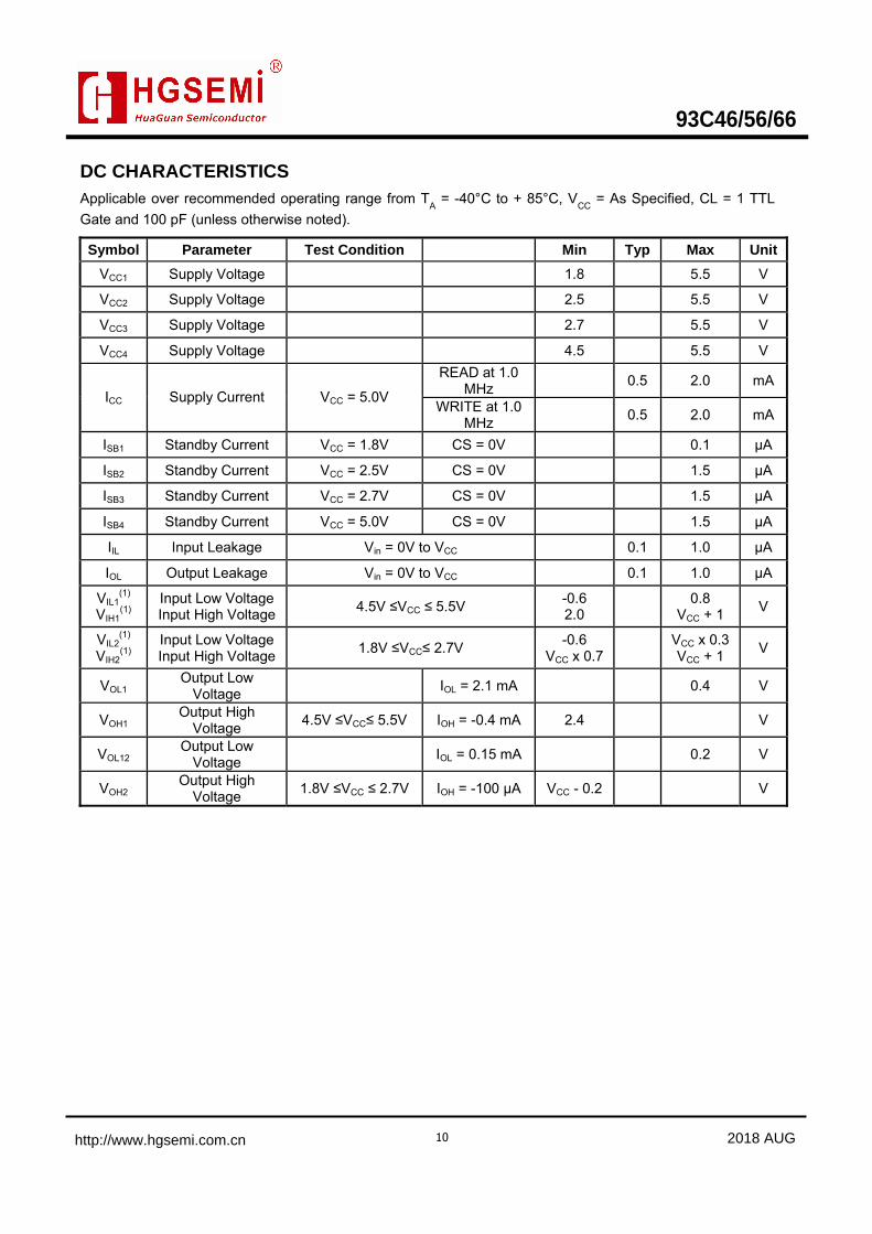
DC CHARACTERISTICS Applicable over recommended operating range from T
A = -40°C to + 85°C, V
CC = As Specified, CL = 1 TTL
Gate and 100 pF (unless otherwise noted).
Symbol Parameter Test Condition Min Typ Max Unit
VCC1 Supply Voltage 1.8 5.5 V
VCC2 Supply Voltage 2.5 5.5 V
VCC3 Supply Voltage 2.7 5.5 V
VCC4 Supply Voltage 4.5 5.5 V
READ at 1.0 MHz
0.5 2.0 mAICC Supply Current VCC = 5.0V
WRITE at 1.0 MHz
0.5 2.0 mA
ISB1 Standby Current VCC = 1.8V CS = 0V 0.1 µA
ISB2 Standby Current VCC = 2.5V CS = 0V 1.5 µA
ISB3 Standby Current VCC = 2.7V CS = 0V 1.5 µA
ISB4 Standby Current VCC = 5.0V CS = 0V 1.5 µA
IIL Input Leakage Vin = 0V to VCC 0.1 1.0 µA
IOL Output Leakage Vin = 0V to VCC 0.1 1.0 µA
VIL1(1)
VIH1(1)
Input Low Voltage Input High Voltage
4.5V ≤VCC ≤ 5.5V -0.6 2.0
0.8
VCC + 1 V
VIL2(1)
VIH2(1)
Input Low Voltage Input High Voltage
1.8V ≤VCC≤ 2.7V -0.6
VCC x 0.7
VCC x 0.3VCC + 1
V
VOL1 Output Low
Voltage IOL = 2.1 mA 0.4 V
VOH1 Output High
Voltage 4.5V ≤VCC≤ 5.5V IOH = -0.4 mA 2.4 V
VOL12 Output Low
Voltage IOL = 0.15 mA 0.2 V
VOH2 Output High
Voltage 1.8V ≤VCC ≤ 2.7V IOH = -100 µA VCC - 0.2 V
93C46/56/66
10 2018 AUGhttp://www.hgsemi.com.cn