2nd half.pdf
31
1 Chapter 1 Introduction 1.1 Embedded system and its requ irement An embedded system is a computer s ystem with a dedicated function within a larger mechanical or electrical system, often with real-time computing constraints. It is embedded as part o f a complete device often including hardware and mechanical parts. By contrast, a general-purpose computer, such as a personal co mputer (PC), is designed to be flexible and to meet a wide range of end-user needs. Embedded systems control many de vices in common use today. Embedded systems contain processing cores that are either microcontrollers or digi tal signal processors (DSP). Requirement of embedded system Easy to use Easy in repair Space e ffi cient Power efficiency Reliable Time saving Simple and cost efficient 1.2 555 timer The 555 timer IC is an integrated circui t (chip) used in a variety of timer, pulse generation, and oscillator applications. The 555 can be used to provide time delays, as a n oscillator, and as a flip-flop element. Derivatives provide up to four t iming circui ts in one package. Three types Astable(none of the state is stable) Bistable- bith the states are stable. Triggering force is needed at both the states. Monostable(input force needed to change state, no force needed to bring back to the original state) 1.3 Flip flop A flip-flop or latch is a circuit that has two stable states and can be used to store state information. A flip-flop is a bistable multivibrator. The circuit can be made to change state by signals applied to one or more co ntrol inputs and will have one or two outputs. It is the basic
-
Upload
siddhant07 -
Category
Documents
-
view
213 -
download
0
Transcript of 2nd half.pdf

8/22/2019 2nd half.pdf
http://slidepdf.com/reader/full/2nd-halfpdf 1/31
1
Chapter 1
Introduction
1.1 Embedded system and its requirement
An embedded system is a computer system with a dedicated function within a larger mechanicalor electrical system, often with real-time computing constraints. It is embedded as part of acomplete device often including hardware and mechanical parts. By contrast, a general-purposecomputer, such as a personal computer (PC), is designed to be flexible and to meet a wide rangeof end-user needs. Embedded systems control many devices in common use today.
Embedded systems contain processing cores that are either microcontrollers or digital signal processors (DSP).
Requirement of embedded system
Easy to use Easy in repair
Space efficient
Power efficiency
Reliable
Time saving
Simple and cost efficient
1.2 555 timer
The 555 timer IC is an integrated circuit (chip) used in a variety of timer, pulse generation,and oscillator applications. The 555 can be used to provide time delays, as an oscillator, andas a flip-flop element. Derivatives provide up to four timing circuits in one package.
Three types
Astable(none of the state is stable)
Bistable- bith the states are stable. Triggering force is needed at both the states.
Monostable(input force needed to change state, no force needed to bring back to theoriginal state)
1.3 Flip flop
A flip-flop or latch is a circuit that has two stable states and can be used to store stateinformation. A flip-flop is a bistable multivibrator. The circuit can be made to change state bysignals applied to one or more control inputs and will have one or two outputs. It is the basic

8/22/2019 2nd half.pdf
http://slidepdf.com/reader/full/2nd-halfpdf 2/31
2
storage element in sequential logic. Flip-flops and latches are a fundamental building block of digital electronics systems used in computers, communications, and many other types of systems.
1.4 Digital clock
Two types-
1. Synchronous- the clock input is same2. Asynchronous- the clock input is different
1.5 Counter
a counter is a device which stores (and sometimes displays) the number of times a particular event or process has occurred, often in relationship to a clock signal.
A counter is always edge triggered
Two types of counter-
1. Positive edge triggered2. Negative edge triggered
Examples of counters are decade counter and up-down counter.
1.6 Classification of microcontroller
1. BITS( 4,8,16,32)2. Memory(embedded, external)3. Instruction set(CISC, RISC)4. Architecture( Vann- Newmann, Harvard)
We have learned about the different Types of sensors
1. IR sensor 2. LDR sensor 3. PIR sensor
4. RF sensor 5. Ultrasonic sensor 6. Photo diode sensor
We also learned as how to generate Custom Character generation and also about to send thedata in the lcd using 4 bit data and finally a project is made using all these concept. In the initial

8/22/2019 2nd half.pdf
http://slidepdf.com/reader/full/2nd-halfpdf 3/31
3
classes we learned to make up – down counter,decade counter, traffic light,keypad using logicgates.
The concept about switch connecting to microcontroller is also made clear to us further theconcept of voltage follower and op-amp is made clear to us.

8/22/2019 2nd half.pdf
http://slidepdf.com/reader/full/2nd-halfpdf 4/31
4
Chapter 2
Company profile
Lovely Professional University (LPU) is a private semi-residential university created under thestate government private university act. LPU claims to be the largest private university in Indiain terms of number of students on a single campus and is situated on 600+ acres of green area on NH-1 at the entry of Jalandhar city. The university has more than 25,000 students from 26 statesand 16 countries. It is recognized by UGC under Section 2(f) of UGC Act 1956.
The Lovely Faculty of Technology and Sciences was ranked #2 on the CSR-GHRDCEngineering Colleges Survey 2011. It was ranked #29 Lovely Professional University wasdeclared as the Best ICT Enabled University of the Year by the Ministry of Communications andIT, Government of India
This summer Lovely Professional University (LPU) has initiated a program called “In HouseSummer Training in Embedded Systems”. This program has helped a lot in educating us ,it
helped in a way to get to know about the technology basically embedded science.
The program initiated from very basic knowledge and on the last day of the training it proved to be a very successful technical program.
The basic knowledge that were imparted to us includes :
2.1 Engineering
Engineering is the application of scientific, economic, social, and practical knowledge in order todesign, build, and maintain structures, machines, devices, systems, materials and processes. It
may encompass using insights to conceive, model and scale an appropriate solution to a problemor objective. The discipline of engineering is extremely broad, and encompasses a range of morespecialized fields of engineering, each with a more specific emphasis on particular areas of technology and types of application.
2.2 Engineer
An engineer is a professional practitioner of engineering, concerned with applying scientificknowledge, mathematics, and ingenuity to develop solutions for technical problems. Engineersdesign materials, structures, and systems while considering the limitations imposed by
practicality, regulation, safety, and cost. To use social, technical and self knowledge to maintainor invent a device for optimum solution.
2.3 Difference between electronics and electrical
Electrical is transmitting or operated by electricity while Electronics are the science developmentand application of devices and systems involving the flow of electrons. Electronics deals withsemiconductor while electrical deals with conductor.

8/22/2019 2nd half.pdf
http://slidepdf.com/reader/full/2nd-halfpdf 5/31
5
2.4 SURFACE MOUNTING DEVICES
Surface-mount technology (SMT) is a method for producing electronic circuits in which thecomponents are mounted or placed directly onto the surface of printed circuit boards (PCBs). Anelectronic device so made is called a surface-mount device (SMD).
2.5 Embedded system
An embedded system is a computer system with a dedicated function within a larger mechanicalor electrical system, often with real-time computing constraints. It is embedded as part of acomplete device often including hardware and mechanical parts. By contrast, a general-purposecomputer, such as a personal computer (PC), is designed to be flexible and to meet a wide rangeof end-user needs. Embedded systems control many devices in common use today.
Embedded systems contain processing cores that are either microcontrollers or digital signal processors (DSP).
These are some of the part of that basic classes and finally on the last day we were done withour final project. The project that I chose is “Digital Speedometer”.
8/22/2019 2nd half.pdf
http://slidepdf.com/reader/full/2nd-halfpdf 6/31
6
Chapter 3
Identification of the training / project
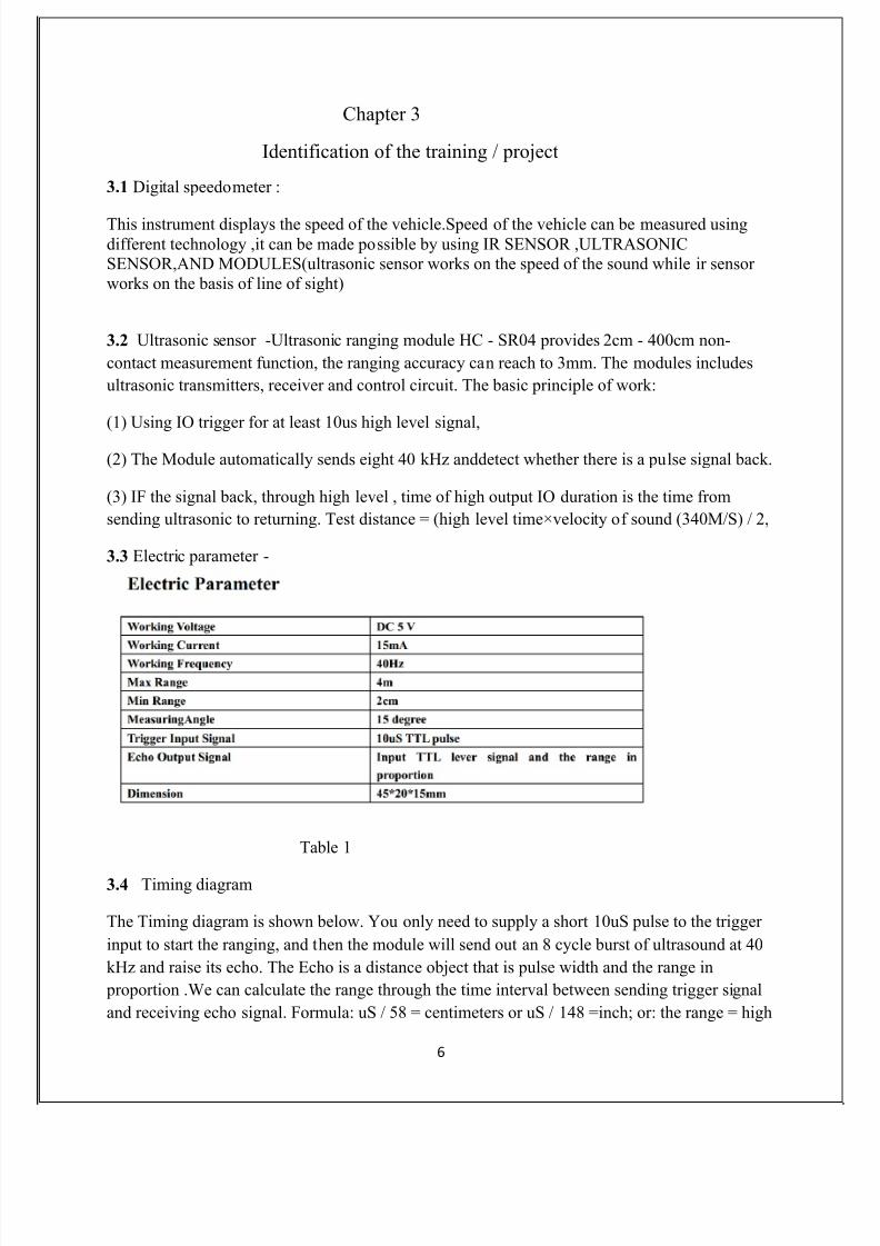
3.1 Digital speedometer :
This instrument displays the speed of the vehicle.Speed of the vehicle can be measured usingdifferent technology ,it can be made possible by using IR SENSOR ,ULTRASONICSENSOR,AND MODULES(ultrasonic sensor works on the speed of the sound while ir sensor works on the basis of line of sight)
3.2 Ultrasonic sensor -Ultrasonic ranging module HC - SR04 provides 2cm - 400cm non-contact measurement function, the ranging accuracy can reach to 3mm. The modules includesultrasonic transmitters, receiver and control circuit. The basic principle of work:
(1) Using IO trigger for at least 10us high level signal,
(2) The Module automatically sends eight 40 kHz anddetect whether there is a pulse signal back.
(3) IF the signal back, through high level , time of high output IO duration is the time fromsending ultrasonic to returning. Test distance = (high level time×velocity of sound (340M/S) / 2,
3.3 Electric parameter -
Table 1
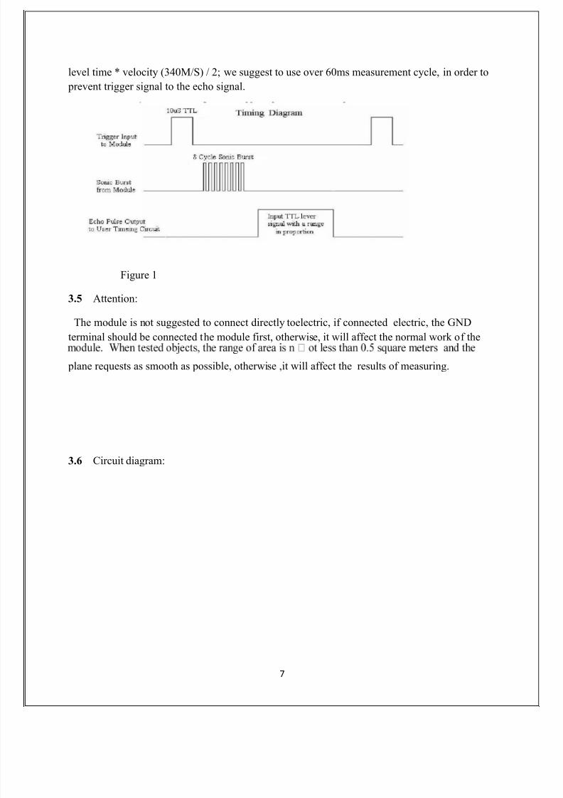
3.4 Timing diagram
The Timing diagram is shown below. You only need to supply a short 10uS pulse to the trigger input to start the ranging, and then the module will send out an 8 cycle burst of ultrasound at 40kHz and raise its echo. The Echo is a distance object that is pulse width and the range in proportion .We can calculate the range through the time interval between sending trigger signaland receiving echo signal. Formula: uS / 58 = centimeters or uS / 148 =inch; or: the range = high
8/22/2019 2nd half.pdf
http://slidepdf.com/reader/full/2nd-halfpdf 7/31
7
level time * velocity (340M/S) / 2; we suggest to use over 60ms measurement cycle, in order to prevent trigger signal to the echo signal.
Figure 13.5 Attention:
The module is not suggested to connect directly toelectric, if connected electric, the GNDterminal should be connected the module first, otherwise, it will affect the normal work of the
plane requests as smooth as possible, otherwise ,it will affect the results of measuring.
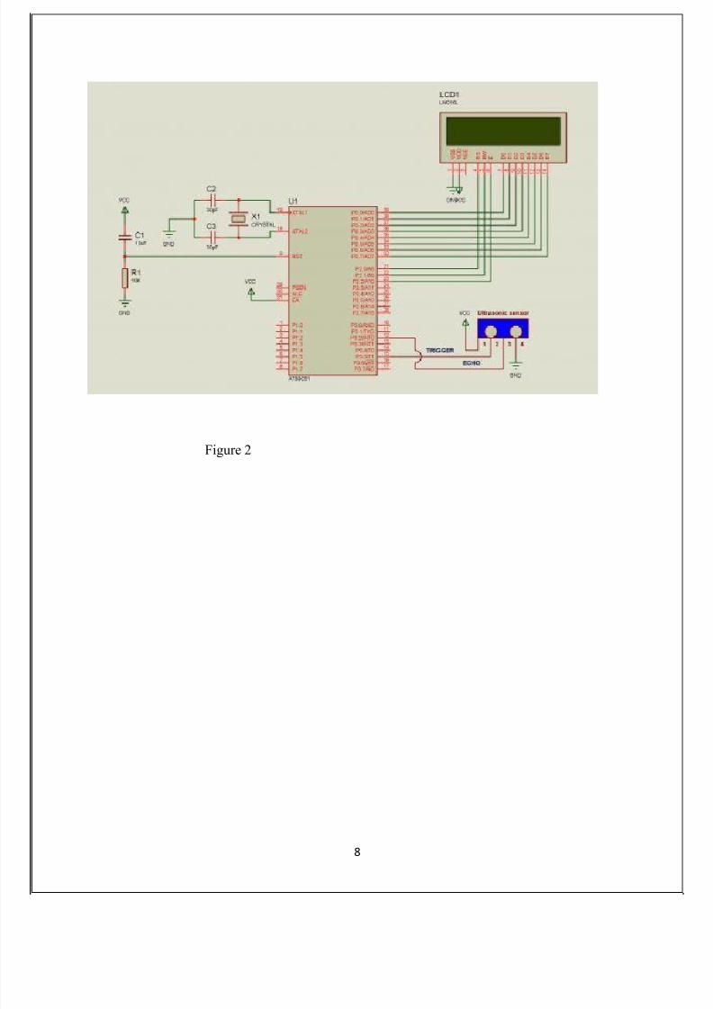
3.6 Circuit diagram:
8/22/2019 2nd half.pdf
http://slidepdf.com/reader/full/2nd-halfpdf 8/31
8
Figure 2
8/22/2019 2nd half.pdf
http://slidepdf.com/reader/full/2nd-halfpdf 9/31
9
CHAPTER 4
IMPLEMENTATION DETAIL
A logic gate is an idealized or physical device implementing a Boolean function, that is, it performs a logical operation on one or more logical inputs, and produces a single logical output.Depending on the context, the term may refer to an ideal logic gate, one that has for instance zerorise time and unlimited fan-out, or it may refer to a non-ideal physical device .
4.1 Circuits using logic gates:
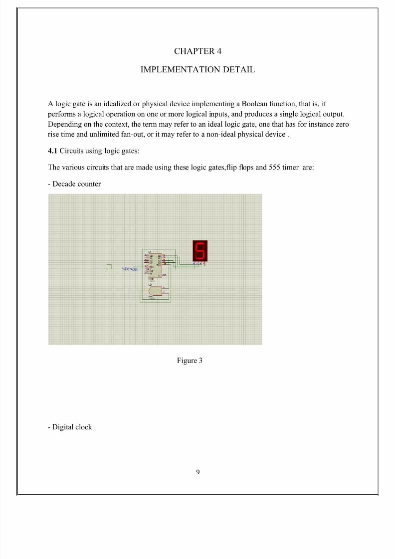
The various circuits that are made using these logic gates,flip flops and 555 timer are:
- Decade counter
Figure 3
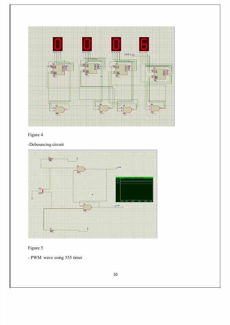
- Digital clock
8/22/2019 2nd half.pdf
http://slidepdf.com/reader/full/2nd-halfpdf 10/31
10
Figure 4
-Debouncing circuit
Figure 5
- PWM wave using 555 timer

8/22/2019 2nd half.pdf
http://slidepdf.com/reader/full/2nd-halfpdf 11/31
11
Figure 6
-Half adder
Figure 7
8/22/2019 2nd half.pdf
http://slidepdf.com/reader/full/2nd-halfpdf 12/31
12
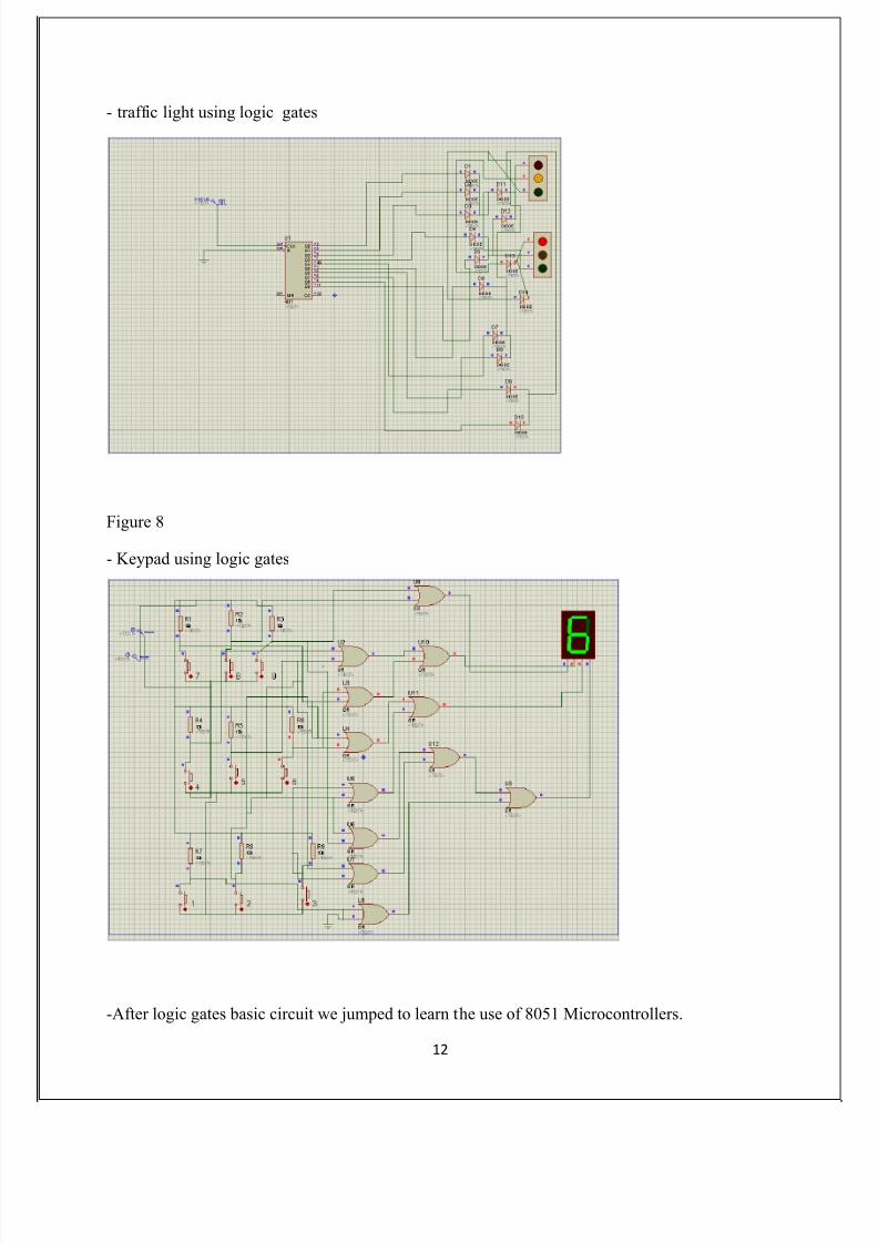
- traffic light using logic gates
Figure 8
- Keypad using logic gates
-After logic gates basic circuit we jumped to learn the use of 8051 Microcontrollers.
8/22/2019 2nd half.pdf
http://slidepdf.com/reader/full/2nd-halfpdf 13/31
13
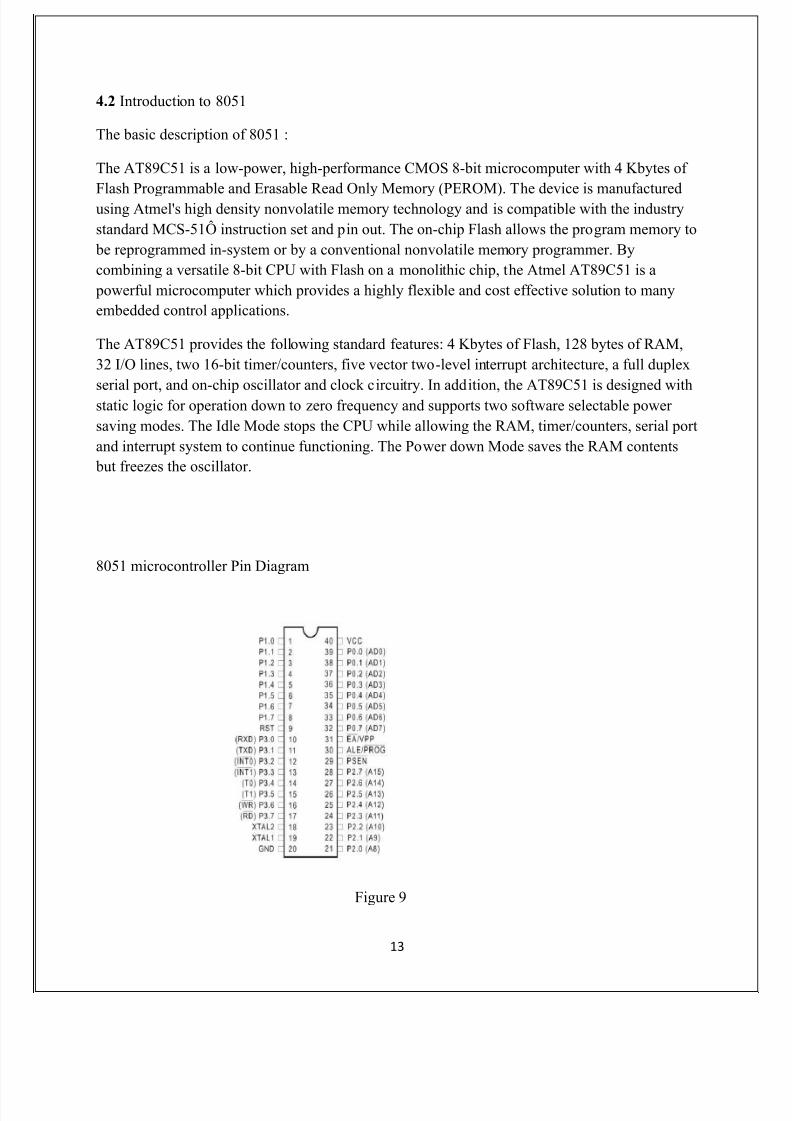
4.2 Introduction to 8051
The basic description of 8051 :
The AT89C51 is a low-power, high-performance CMOS 8-bit microcomputer with 4 Kbytes of
Flash Programmable and Erasable Read Only Memory (PEROM). The device is manufacturedusing Atmel's high density nonvolatile memory technology and is compatible with the industrystandard MCS-51Ô instruction set and pin out. The on-chip Flash allows the program memory to be reprogrammed in-system or by a conventional nonvolatile memory programmer. Bycombining a versatile 8-bit CPU with Flash on a monolithic chip, the Atmel AT89C51 is a powerful microcomputer which provides a highly flexible and cost effective solution to manyembedded control applications.
The AT89C51 provides the following standard features: 4 Kbytes of Flash, 128 bytes of RAM,32 I/O lines, two 16-bit timer/counters, five vector two-level interrupt architecture, a full duplex
serial port, and on-chip oscillator and clock circuitry. In addition, the AT89C51 is designed withstatic logic for operation down to zero frequency and supports two software selectable power saving modes. The Idle Mode stops the CPU while allowing the RAM, timer/counters, serial portand interrupt system to continue functioning. The Power down Mode saves the RAM contents but freezes the oscillator.
8051 microcontroller Pin Diagram
Figure 9

8/22/2019 2nd half.pdf
http://slidepdf.com/reader/full/2nd-halfpdf 14/31
14
4.3 Pin Functions:-
ALE/PROG: Address Latch Enable output pulse for latching the low byte of the address duringaccesses to external memory. ALE is emitted at a constant rate of 1/6 of the oscillator frequency,for external timing or clocking purposes, even when there are no accesses to external memory.(However, one ALE pulse is skipped during each access to external Data Memory.) This pin isalso the program pulse input (PROG) during EPROM programming.
PSEN: Program Store Enable is the read strobe to external Program Memory. When the device isexecuting out of external Program Memory, PSEN is activated twice each machine cycle (exceptthat two PSEN activations are skipped during accesses to external Data Memory). PSEN is not
activated when the device is executing out of internal Program Memory.
EA/VPP: When EA is held high the CPU executes out of internal Program Memory (unless theProgram Counter exceeds 0FFFH in the 80C51). Holding EA low forces the CPU to execute outof external memory regardless of the Program Counter value. In the 80C31, EA must beexternally wired low. In the EPROM devices, this pin also receives the programming supplyvoltage (VPP) during EPROM programming.
XTAL1: Input to the inverting oscillator amplifier.XTAL2: Output from the inverting oscillator amplifier.
Port 0: Port 0 is an 8-bit open drain bidirectional port. As an open drain output port, it can sink eight LS TTL loads. Port 0 pins that have 1s written to them float, and in that state will functionas high impedance inputs.Port 1: Port 1 is an 8-bit bidirectional I/O port with internal pull-ups. Port 1 pins that have 1swritten to them are pulled high by the internal pull-ups, and in that state can be used as inputs.As inputs, port 1 pins that are externally being pulled low will source current because of theinternal pull-ups.Port 2: Port 2 is an 8-bit bidirectional I/O port with internal pull-ups. Port 2 emits the high-order
address byte during accesses to external memory that use 16-bit addresses. In this application, ituses the strong internal pull-ups when emitting 1s.Port 3: Port 3 is an 8-bit bidirectional I/O port with internal pull-ups. It also serves the functionsof various special features of the 80C51 FamilyVCC: Supply voltageVSS: Circuit ground potential

8/22/2019 2nd half.pdf
http://slidepdf.com/reader/full/2nd-halfpdf 15/31
15
Port Structures and Operation:-
All four ports in the 80C51 are bidirectional. Each consists of a latch (Special Function RegistersP0 through P3), an output driver, and an input buffer. The output drivers of Ports 0 and 2, and theinput buffers of Port 0, are used in accesses to external memory. In this application, Port 0
outputs the low byte of the external memory address, time-multiplexed with the byte beingwritten or read. Port 2 outputs the high byte of the external memory address when the address is16 bits wide. Otherwise, the Port 2 pins continue to emit the P2 SFR content.All the Port 3 pins are multifunctional. They are not only port pins, but also serve the functionsof various special features as listed below:
Port Pin Alternate Function:-P3.0 RxD (serial input port)P3.1 TxD (serial output port)
P3.2 INT0 (external interrupt)P3.3 INT1 (external interrupt)P3.4 T0 (Timer/Counter 0 external input)P3.5 T1 (Timer/Counter 1 external input)P3.6 WR (external Data Memory write strobe)P3.7 RD (external Data Memory read strobe)The alternate functions can only be activated if the corresponding bit latch in the port SFR contains a 1. Otherwise the port pin remains at 0.
4.4 Special Function Registers (SFRs):-
A Map of the on-chip memory area called the Special FunctionRegister (SFR).In the SFRs not all of the addresses are occupied. Unoccupied addresses are notimplemented on the chip. Read accesses to these addresses will in general return random data,and write accesses will have no effect. User software should not write 1s to these unimplementedlocations, since they may be used in other 80C51 Family derivative productsto invoke new features. The functions of the SFRs are described in the text that follows.
Accumulator:ACC is the Accumulator register. The mnemonics for Accumulator-Specific instructions,however, refer to the Accumulator simply as A.B Register:The B register is used during multiply and divide operations. For other instructions it can betreated as another scratch pad register.Program Status Word:
8/22/2019 2nd half.pdf
http://slidepdf.com/reader/full/2nd-halfpdf 16/31
16
The PSW register contains program status information as detailed in Figure.
4.5 Stack Pointer:-
The Stack Pointer register is 8 bits wide. It is incremented before data is stored during PUSH andCALL executions. While the stack may reside anywhere in on-chip RAM, the Stack Pointer isinitialized to 07H after a reset. This causes the stack to begin at locations 08H.
4.6 Data Pointer:-The Data Pointer (DPTR) consists of a high byte (DPH) and a low byte (DPL). Its intendedfunction is to hold a 16-bit address. It may be manipulated as a 16-bit register or as twoindependent 8-bit registers.
4.7 Serial Data Buffer:-
The Serial Buffer is actually two separate registers, a transmit buffer and a receive buffer. Whendata is moved to SBUF, it goes to the transmit buffer and is held for serial transmission. (Movinga byte to SBUF is what initiates the transmission.) When data is moved from SBUF, it comesfrom the receive buffer.
4.8 Timer Registers Basic to 80C51:-Register pairs (TH0, TL0), and (TH1, TL1) are the 16-bit Counting registers for Timer/Counters0 and 1, respectively.
4.9 Control Register for the 80C51:-
Special Function Registers IP, IE, TMOD, TCON, SCON, and PCON contain control and status bits for the interrupt system, the Timer/Counters, and the serial port. They are described in later sections.
4.10 Basic Registers:-
A number of 8052 registers can be considered "basic." Very little can be done without them anda detailed explanation of each one is warranted to make sure the reader understands theseregisters before getting into more complicated areas of development.
4.11 The Accumulator:-If you've worked with any other assembly language you will be familiar with the concept of anaccumulator register.The Accumulator, as its name suggests, is used as a general register to accumulate the results of a large number of instructions. It can hold an 8-bit (1-byte) value and is the most versatile

8/22/2019 2nd half.pdf
http://slidepdf.com/reader/full/2nd-halfpdf 17/31
17
register the 8052 has due to the sheer number of instructions that make use of the accumulator.More than half of the 8052's 255 instructions manipulate or use the Accumulator in some way.For example, if you want to add the number 10 and 20, the resulting 30 will be stored in theAccumulator. Once you have a value in the Accumulator you may continue processing the valueor you may store it in another register or in memory.
4.12 The Program Counter:-
The Program Counter (PC) is a 2-byte address that tells the 8052 where the next instruction toexecute is found in memory. When the 8052 is initialized PC always starts at 0000h and isincremented each time an instruction is executed. It is important to note that PC isn't alwaysincremented by one. Since some instructions are 2 or 3 bytes in length the PC will beincremented by 2 or 3 in these cases.The Program Counter is special in that there is no way to directly modify its value. That is to say,
you can't do something like PC=2430h. On the other hand, if you execute LJMP 2430h you'veeffectively accomplished the same thing.It is also interesting to note that while you may change the value of PC (by executing a jumpinstruction, etc.) there is no way to read the value of PC. That is to say, there is no way to ask the8052 "What address are you about to execute?" As it turns out, this is not completely true: Thereis one trick that may be used to determine the current value of PC. This trick will be covered in alater chapter.
4.13 The Data Pointer:-
The Data Pointer (DPTR) is the 8052ís only user-accessible 16-bit (2-byte) register. TheAccumulator, "R" registers, and "B" register are all 1-byte values. The PC just described is a 16- bit value but isn't directly user-accessible as a working register.DPTR, as the name suggests, is used to point to data. It is used by a number of commands thatallow the 8052 to access external memory. When the 8052 accesses external memory it accessesthe memory at the address indicated by DPTR.While DPTR is most often used to point to data in external memory or code memory, manydevelopers take advantage of the fact that it's the only true 16-bit register available. It is oftenused to store 2-byte values that have nothing to do with memory locations.
4.14 Addressing Modes:-The addressing modes in the 80C51 instruction set are as follows:Direct Addressing:-In direct addressing the operand is specified by an 8-bit address field in the instruction. Onlyinternal Data RAM and SFRs can be directly addressed.Indirect Addressing:-

8/22/2019 2nd half.pdf
http://slidepdf.com/reader/full/2nd-halfpdf 18/31
18
In indirect addressing the instruction specifies a register which contains the address of theoperand. Both internal and external RAM can be indirectly addressed. The address register for 8- bit addresses can be R0 or R1 of the selected bank, or the Stack Pointer. The address register for 16-bit addresses can only be the 16- bit “data pointer” register, DPTR. Register Instructions:-
The register banks, containing registers R0 through R7, can be accessed by certain instructionswhich carry a 3-bit register specification within the opcode of the instruction. Instructions thataccess the registers this way are code efficient, since this mode eliminates an address byte. Whenthe instruction is executed, one of the eight registers in the selected bank is accessed. One of four banks is selected at execution time by the two bank select bits in the PSW.
Register-Specific Instructions:-Some instructions are specific to a certain register. For example, some instructions alwaysoperate on the Accumulator, or Data Pointer, etc., so no address byte is needed to point to it. The
opcode itself does that. Instructions that refer to the Accumulator as A assemble as accumulator specific opcodes.Immediate Constants:-The value of a constant can follow the opcode in Program Memory.For example,MOV A, #100Loads the Accumulator with the decimal number 100. The same number could be specified inhex digits as 64H.Indexed Addressing:-Only program Memory can be accessed with indexed addressing, and it can only be read. This
addressing mode is intended for reading look-up tables in Program Memory A 16-bit baseregister (either DPTR or the Program Counter) points to the base of the table, and theAccumulator is set up with the table entry number. The address of the table entry in ProgramMemory is formed by adding the Accumulator data to the base pointer. Another type of indexedaddressing is used in the “case jump” instruction. In this case the destination address of a jump
instruction is computed as the sum of the base pointer and the Accumulator data.
4.15 Project done in training period:Digital speedometer:
This instrument displays the speed of the vehicle.Speed of the vehicle can be measured usingdifferent technology ,it can be made possible by using IR SENSOR ,ULTRASONICSENSOR,AND MODULES(ultrasonic sensor works on the speed of the sound while ir sensor works on the basis of line of sight)
The main components used here in this project are LCD,ULTRASONIC SENSOR,8051MICROCONTROLLER etc

8/22/2019 2nd half.pdf
http://slidepdf.com/reader/full/2nd-halfpdf 19/31
19
Figure 10
PIN No. SYMBOL I/O DISCRIPTION
1 Vss -- GROUNDED
2 Vcc -- +5V POWER SUPPLY
3 Vee -- Power supply to control contrast
4 RS I RS=0,select command register
RS=1,select data register
5 R/W I R/W=0,for write
R/W=1,for read
6 E I/O Enable
7-14 DB0 I/O The 8 bit data bus
Table 2
Circuit Description
1 2 3 4 5 6 7 8 9 10 11 12 13 14 15 16
L.C.D.
Vss VccVee RSR/W E DB0DB1DB2 DB3DB4DB5DB6 DB7LED+LED-
PIN DIAGRAM OF L.C.D.

8/22/2019 2nd half.pdf
http://slidepdf.com/reader/full/2nd-halfpdf 20/31
20
In this interfacing we use the port 1 as a LCD control and port 2 as a LCD data. Switchesconnected on port 3 and LED connected on port 1. Whenever we use port 0 we have to connect pull up register externally to make it by directional because of by default port 0 is unidirectionali.e. only input port .
All other ports have already inbuilt pull up register so no need to connect pull up register externally.
P3.2 is used as external timer 0 interrupt connected to echo pin of ultrasonic sensor , P3.5 isused as triggering pin connected to triggering pin of ultrasonic sensor
CONNECTION OF PULLUP REGISTER
Figure 11
Port 0 is also designated as AD0 – AD7 allowing it to be used for both address and data whenconnection and 8051 to an external memory port 0 provides both address and data .The 8051multiplexes address and data through port 0 to save pins.
ALE indicates if port 0 as address or data .When ALE=0 it provides data D0-D7 but when
ALE=1 it has address A0-A7.Therefore ALE is used for demultiplexing address and data withthe help of a 74LS 373 latch. In 8051 based system where there is no external memoryconnection, the pins of port 0 must be connected externally to a 10k ohm pull-up register. This isdue to fact that port 0 each and opens drain, unlike port1, port2 and port3.
The 8051 has on chip oscillator but requires an external clock to run it. Most often a quartzcrystal oscillator is connected to inputs XTAL1 and XTAL2. The quartz crystal oscillator connected to XTAL1 and XTAL2 also needs two capacitor of 30pF value. One side of eachcapacitor is connected to the ground
List of hardware.
S.NO. Name of Hardware. Quantity
1. 40 pin IC base 1
2. 8051 microcontroller 1
8/22/2019 2nd half.pdf
http://slidepdf.com/reader/full/2nd-halfpdf 21/31
21
3. XTAL(11.0592Mhz) 1
4. Capacitor 33pF 2
5. 10k POT 1
6. LCD 1
7. 7085 regulator 1
8. Pull-up resistor 1
9. G.P. PCB 1
10. Berg strip As required.
11. ULTRA SONIC SENSOR 1
12. Wires As required
13. Resistance As required
14. Multimeter
15. 12v DC supply source 1
16. Soldering wires, soldering iron ,Flux
Table 3
8/22/2019 2nd half.pdf
http://slidepdf.com/reader/full/2nd-halfpdf 22/31
22
Chapter 5
Result and future scope
5.1 Conclusion:
Knowing about the microcontroller has always been the matter of excitement for all of us. Andsummer training during the June 2013 was the one of the good opportunity to fulfill this. Thetraining was as fruitful as expected.
There we got the exposure about the 8051 microcontroller and its various basic electronicscomponents used in developing an embedded system. We worked on keil tool software which isused to developed program for embedded system. The work experience in the AdvancedTechnology was quite nice. The trainers those were assigned to us were quite experience.
The aim of our experiment is to create an efficient low cost Digital Speedometer. It was inspired by the fact that most of the modern-day vehicles use analog speedometers which have resolutionof about 5kmph and the range is also limited.
5.2 Future scope
Historically auto motive vehicles have been provided with mechanical speedometers in which
rotation of wheel of the vehicle or of a drive component of the transmission is transmitted as atorsional impulse the torsional force applied to the cable is typically transmitted to needle in theinstrument panel which is deflected across a scale to indicate speed at which vehicle is travelling.The Principal dis advantage with such systems has been the requirement for a signal generatingsystem independent of the conventional mechanical speedometer system associated with the automobile. It increases the cost of the vehicle.The Digital Speedometer we have designed can measure up to a speed of 999kmph with aresolution of 1kmph. It‟s rather inexpensive and can be used in almost all vehicles.

8/22/2019 2nd half.pdf
http://slidepdf.com/reader/full/2nd-halfpdf 23/31
23
REFERENCES:
1. http://www.Electronicsforu.com2. http://www .Circuiteasy.com3. http://www.8051projects.com
4.
http://www.electronics-lab.com5. http://www.microntroller.com6. http://www.wisc-online.com7. http://www.seminarprojects.com8. http://www.allaboutcircuits.com9. http://www.nptel.iitm.ac.in10. 10.BOOK ON EMBEDDEDSYSTEM BY MAZIDI11. 11.8051 MC ARCH,PROGRAM AND APPLICATION-KENNATH J AYALA
8/22/2019 2nd half.pdf
http://slidepdf.com/reader/full/2nd-halfpdf 24/31
24
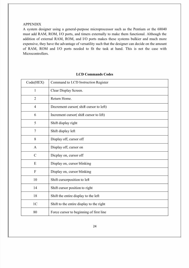
APPENDIXA system designer using a general-purpose microprocessor such as the Pentium or the 68040must add RAM, ROM, I/O ports, and timers externally to make them functional. Although theaddition of external RAM, ROM, and I/O ports makes these systems bulkier and much moreexpensive, they have the advantage of versatility such that the designer can decide on the amount
of RAM, ROM and I/O ports needed to fit the task at hand. This is not the case withMicrocontrollers.
LCD Commands Codes
Code(HEX) Command to LCD Instruction Register
1 Clear Display Screen.
2 Return Home.
4 Decrement cursor( shift cursor to left)
6 Increment cursor( shift cursor to lift)
5 Shift display right
7 Shift display left
8 Display off, cursor off A Display off, cursor on
C Dicplay on, cursor off
E Display on, cursor blinking
F Display on, cursor blinking
10 Shift cursorposition to left
14 Shift cursor position to right
18 Shift the entire display to the left
1C Shift to the entire display to the right
80 Force cursor to beginning of first line
8/22/2019 2nd half.pdf
http://slidepdf.com/reader/full/2nd-halfpdf 25/31
25
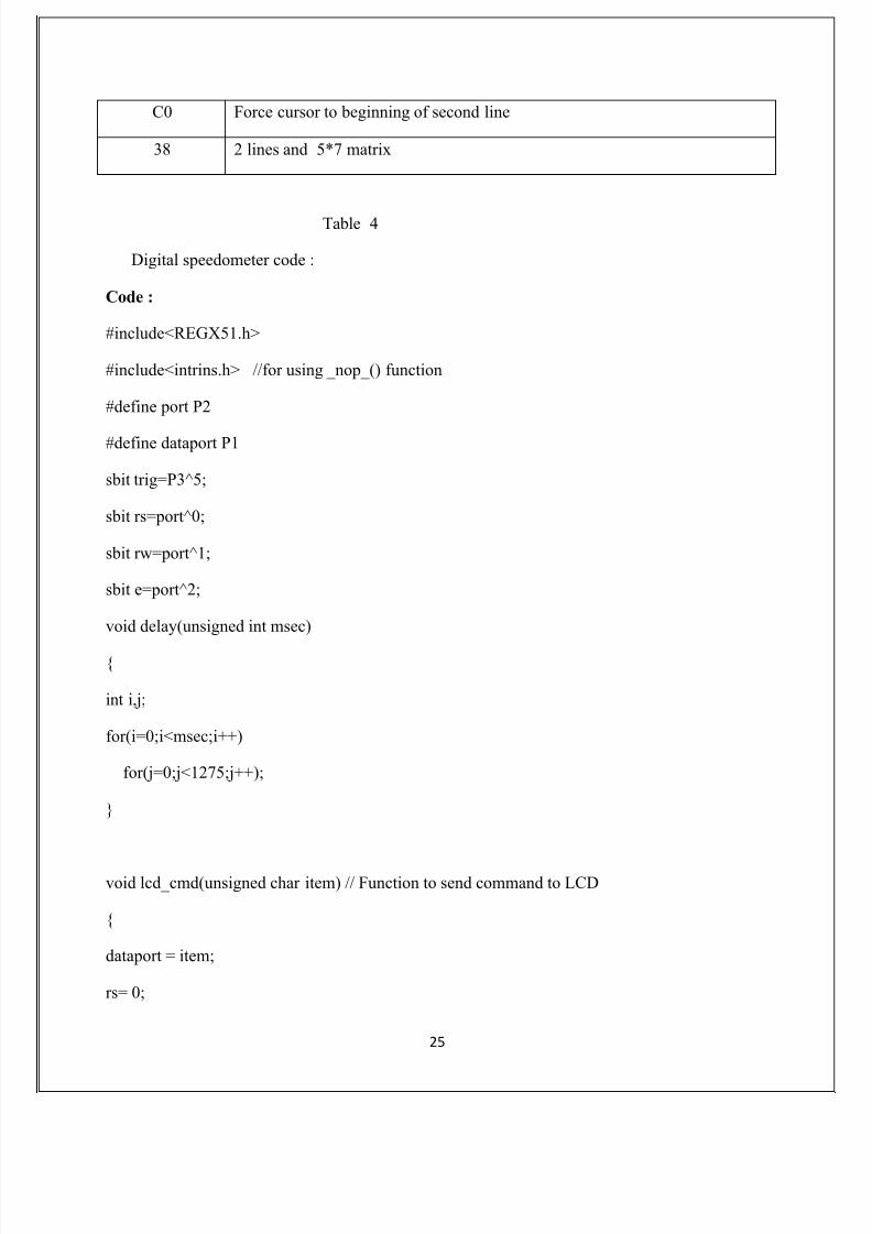
C0 Force cursor to beginning of second line
38 2 lines and 5*7 matrix
Table 4
Digital speedometer code :
Code :
#include<REGX51.h>
#include<intrins.h> //for using _nop_() function
#define port P2
#define dataport P1
sbit trig=P3^5;
sbit rs=port^0;
sbit rw=port^1;
sbit e=port^2;
void delay(unsigned int msec)
{
int i,j;
for(i=0;i<msec;i++)
for(j=0;j<1275;j++);
}
void lcd_cmd(unsigned char item) // Function to send command to LCD
{
dataport = item;
rs= 0;

8/22/2019 2nd half.pdf
http://slidepdf.com/reader/full/2nd-halfpdf 26/31
26
rw=0;
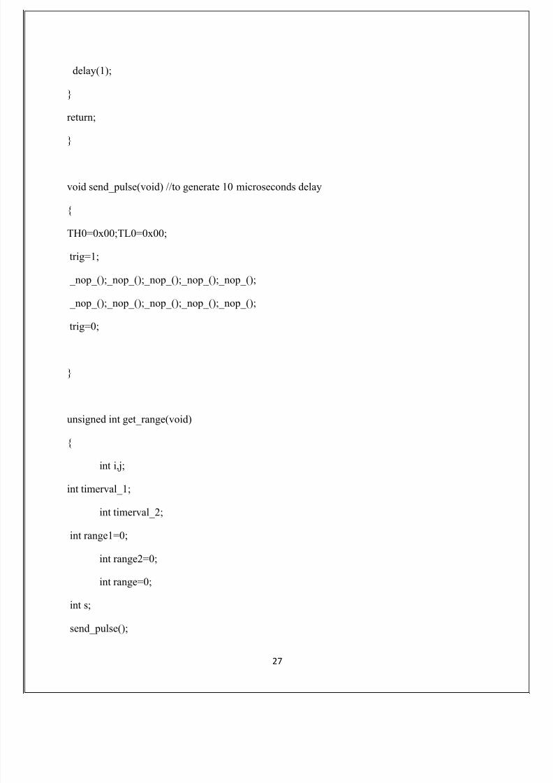
e=1;
delay(1);
e=0;
return;
}
void lcd_data(unsigned char item) // Function to send data to LCD
{
dataport = item;
rs= 1;
rw=0;
e=1;
delay(1);
e=0;
return;
}
void lcd_data_string(unsigned char *str) // Function to send string to LCD
{
int i=0;
while(str[i]!='\0')
{
lcd_data(str[i]);
i++;
8/22/2019 2nd half.pdf
http://slidepdf.com/reader/full/2nd-halfpdf 27/31
27
delay(1);
}
return;
}
void send_pulse(void) //to generate 10 microseconds delay
{
TH0=0x00;TL0=0x00;
trig=1;
_nop_();_nop_();_nop_();_nop_();_nop_();
_nop_();_nop_();_nop_();_nop_();_nop_();
trig=0;
}
unsigned int get_range(void)
{
int i,j;
int timerval_1;
int timerval_2;
int range1=0;
int range2=0;
int range=0;
int s;
send_pulse();

8/22/2019 2nd half.pdf
http://slidepdf.com/reader/full/2nd-halfpdf 28/31
28
delay(40);
timerval_1 = TH0;
timerval_1 = (timerval_1 << 8) | TL0;
TH0=0xFF;TL0=0xFF;
range1=timerval_1/59; // to get distance ( in cm )
for(i=0;i<500;i++) // 0.5 sec delay
for(j=0;j<1275;j++);
send_pulse();
delay(40);
timerval_2= TH0;
timerval_2 = (timerval_2 << 8) | TL0;
TH0=0xFF;TL0=0xFF;
range2=timerval_2/59;
range= range2-range1;
if(range<35000)
{//actually you need to use 38000 but the sensor may not work at higher levels
range = (range * 0.02 ) ;// there is a delay of 0.5 sec therefore the distance ( cm --> m )is to be divided by time ( 0.5 sec )
s=range/100;
range=range%100;
lcd_cmd(0x81);
delay(2);
lcd_data_string("output:(m/s)");
delay(2);
lcd_cmd(0x8a);

8/22/2019 2nd half.pdf
http://slidepdf.com/reader/full/2nd-halfpdf 29/31
29
delay(2);
if(s!=0)
{
lcd_cmd(0x06);
delay(2);
lcd_data(s+48);
delay(2);
s=range;
range=range/10;
lcd_data(range+48);
delay(2);
s=s%10;
lcd_data(s+48);
delay(2);
}
else
{
lcd_cmd(0x06);
s=range/10;
range=range%10;
lcd_data(s+48);
delay(2);
lcd_data(range+48);
delay(2);
8/22/2019 2nd half.pdf
http://slidepdf.com/reader/full/2nd-halfpdf 30/31
30
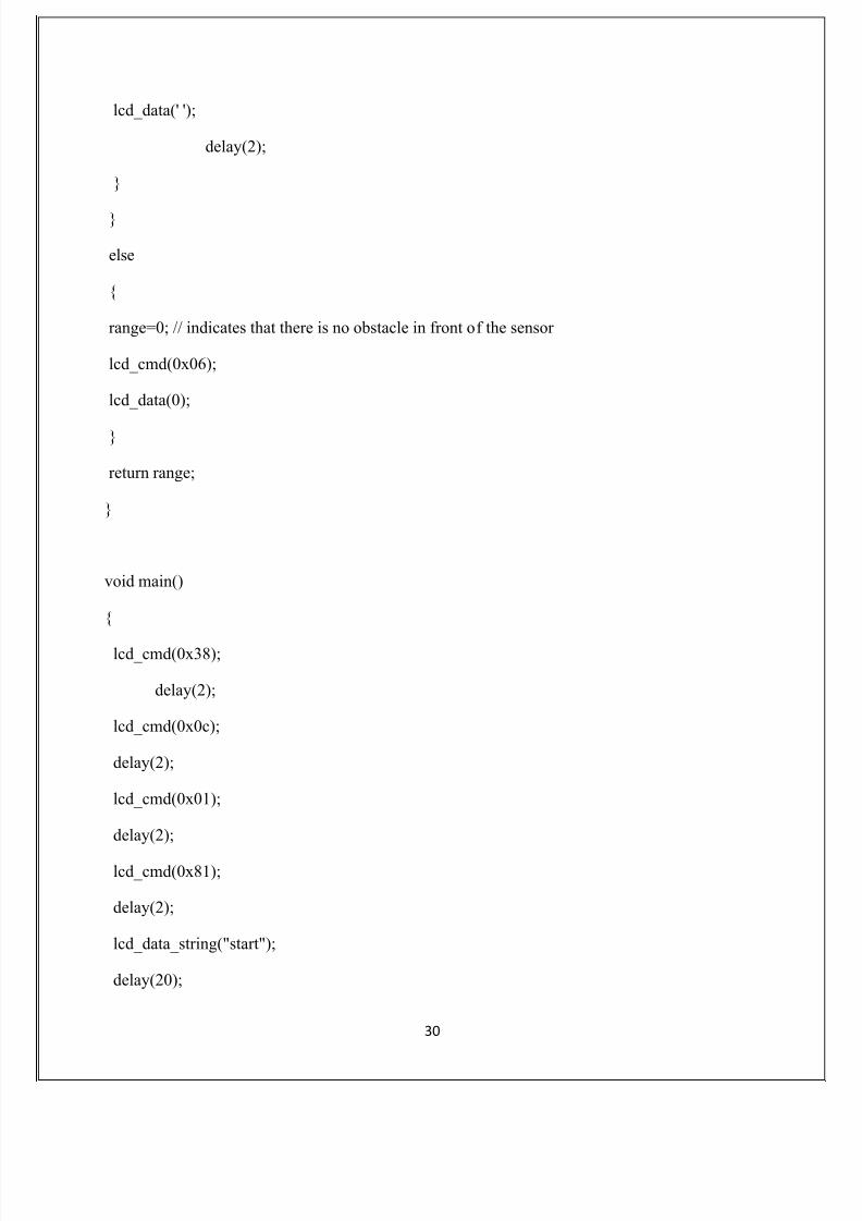
lcd_data(' ');
delay(2);
}
}
else
{
range=0; // indicates that there is no obstacle in front of the sensor
lcd_cmd(0x06);
lcd_data(0);
}
return range;
}
void main()
{
lcd_cmd(0x38);
delay(2);
lcd_cmd(0x0c);
delay(2);
lcd_cmd(0x01);
delay(2);
lcd_cmd(0x81);
delay(2);
lcd_data_string("start");
delay(20);

8/22/2019 2nd half.pdf
http://slidepdf.com/reader/full/2nd-halfpdf 31/31
TMOD=0x09;//timer0 in 16 bit mode with gate enable
TR0=1;//timer run enabled
TH0=0x00;TL0=0x00;
P3=0x04;//setting pin P3.2 ( INT0 )
while(1)
{
get_range();
}