The Characterization of Graphene Paper for Flexible Electronics Application

April 15, 2015 www.tu-ilmenau.dePage 1
Frontiers of Characterization and Metrology for Nanoelectronics
FCMN Hilton Dresden Downtown, Dresden, Germany, 14‐16 April 2015
2D Materials Beyond
GrapheneFor Future Electronics
Frank Schwierz, Technische Universität Ilmenau, Germany
•
Introduction
•
An (Incomplete) Overview of 2D Materials
•
2D Transistors –
State of the Art‐
2D Transistors for More Moore
‐
2D Transistors for More Than Moore
•
Metrology Needs for 2D Transistors and 2D Electronics
•
Conclusion
April 15, 2015 www.tu-ilmenau.dePage 2
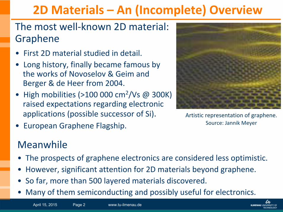
Meanwhile•
The prospects of graphene electronics are considered less optimistic.
•
However, significant attention for 2D materials beyond graphene.•
So far, more than 500 layered materials discovered.
•
Many of them semiconducting and possibly useful for electronics.
2D Materials – An (Incomplete) OverviewThe most well‐known 2D material: Graphene•
First 2D material studied in detail.
•
Long history, finally became famous by the works of Novoselov & Geim and Berger & de Heer from 2004.
•
High mobilities (>100 000 cm2/Vs @ 300K) raised expectations regarding electronic applications (possible successor of Si).
•
European Graphene
Flagship.Artistic
representation
of graphene.Source: Jannik Meyer
April 15, 2015 www.tu-ilmenau.dePage 3
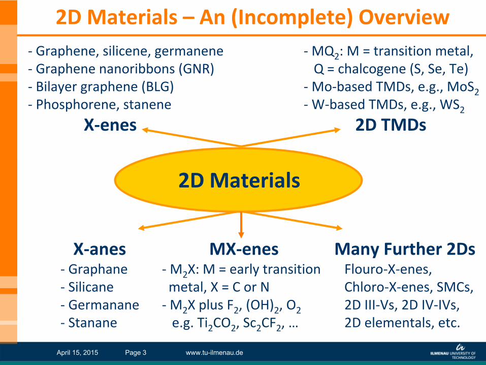
‐
Graphene, silicene, germanene‐
Graphene nanoribbons
(GNR)
‐
Bilayer
graphene
(BLG)‐ Phosphorene, stanene
X‐enes
‐
MQ2
: M = transition metal,Q = chalcogene
(S, Se, Te)
‐Mo‐based TMDs, e.g., MoS2‐W‐based TMDs, e.g., WS2
2D TMDs
2D Materials – An (Incomplete) Overview
2D Materials
Many Further 2Ds Flouro‐X‐enes, Chloro‐X‐enes, SMCs, 2D III‐Vs, 2D IV‐IVs, 2D elementals, etc.
MX‐enes‐M2
X: M = early transition metal, X = C or N‐
M2
X plus F2
, (OH)2
, O2e.g. Ti2
CO2
, Sc2
CF2
, …
X‐anes‐ Graphane‐ Silicane‐ Germanane‐ Stanane

April 15, 2015 www.tu-ilmenau.dePage 4
2D Materials – An (Incomplete) Overview
No gap, EG
= 0! This
is really
a pitty, since
the
missing
gap
causes serious
problems
for
transistors.
Conduction band
Valence bandBandgap
EG
EG
≤
130 meVToo
narrow
for
logic
tran‐sistors.
Energy
Wave vector
X‐enes‐ Graphene‐ Silicene‐ Germanene
BLG X‐enes
X‐anes‐ Phosphorene
‐
Graphane
‐ Stanene
‐
Silicane
‐
GNRs
‐
Germanane
MX‐enes 2D TMDs
‐ Sc2
CF2
‐
MoS2
, MoSe2
, MoTe2‐ TiCO2
‐
WS2
, WSe2
, WTe2
etc., etc.Many
of these
materials
have
a gap
EG
= 0.5…
2.5 eV, perfect
fortransistors.

April 15, 2015 www.tu-ilmenau.dePage 5
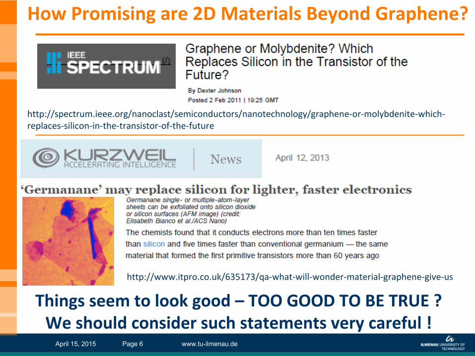
How
Promising
are
2D Materials Beyond
Graphene?
http://www.bbc.co.uk/news/technology‐16034693
April 15, 2015 www.tu-ilmenau.dePage 6
http://www.itpro.co.uk/635173/qa‐what‐will‐wonder‐material‐graphene‐give‐us
http://spectrum.ieee.org/nanoclast/semiconductors/nanotechnology/graphene‐or‐molybdenite‐which‐replaces‐silicon‐in‐the‐transistor‐of‐the‐future
Things seem to look good – TOO GOOD TO BE TRUE ?We should consider such statements very careful !
How
Promising
are
2D Materials Beyond
Graphene?
April 15, 2015 www.tu-ilmenau.dePage 7
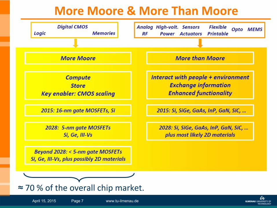
More
Moore & More
Than
Moore
≈
70 % of the
overall
chip
market.
April 15, 2015 www.tu-ilmenau.dePage 8
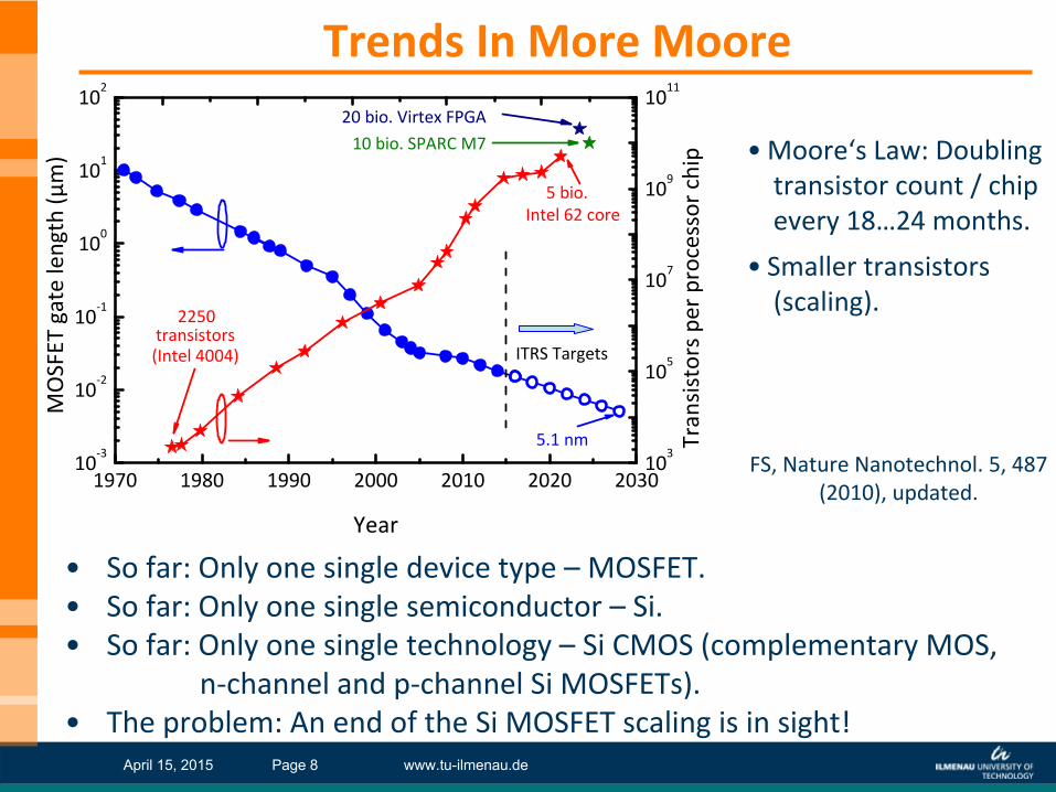
Trends In More Moore
•
So far: Only one single device type – MOSFET.•
So far: Only one single semiconductor – Si.
•
So far: Only one single technology – Si CMOS (complementary MOS, n‐channel and p‐channel Si MOSFETs).
•
The
problem: An end of the
Si MOSFET scaling
is
in sight!
•
Moore‘s Law: Doubling transistor count / chip every 18…24 months.
•
Smaller transistors (scaling).
FS, Nature Nanotechnol. 5, 487
(2010), updated.1970 1980 1990 2000 2010 2020 203010
‐3
10‐2
10‐1
100
101
102
103
105
107
109
1011
ITRS Targets
MOSFET
gate length (µ
m)
Year
20 bio. Virtex FPGA
Intel 62 core
transistors(Intel 4004)
10 bio. SPARC M7
2250
Transistors pe
r processor chip
5 bio.
5.1 nm
April 15, 2015 www.tu-ilmenau.dePage 9
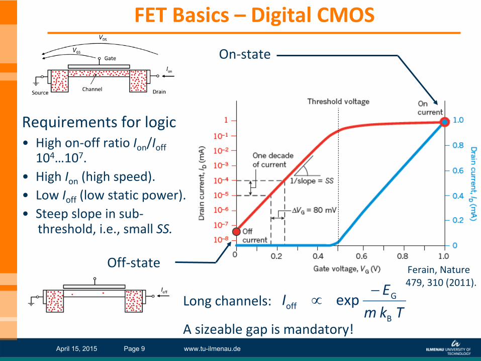
On‐state
FET Basics –
Digital CMOS
Ferain, Nature 479, 310 (2011).
Requirements
for
logic•
High on‐off
ratio
Ion
/Ioff104…107.
•
High Ion
(high speed).•
Low
Ioff
(low
static
power).•
Steep
slope
in sub‐
threshold, i.e., small
SS.
Off‐state
TkmE
IB
Goff exp
Long channels:
A sizeable
gap
is
mandatory!
April 15, 2015 www.tu-ilmenau.dePage 10
High on‐current
Ion• High carrier mobility µ
needed, introduction
of high‐µ
light‐meff
channels.
Low
off‐current
Ioff
and small
SS• Good electrostatic integrity
required
to suppress
short‐channel
effects, a
short
scale
length
is
beneficial.
• Suppression of direct
source‐drain
tunneling.‐
Currently
(L
≥
10 nm) not
a problem.
‐
Will become
an issue
at ultra‐short
gate
length
levels.
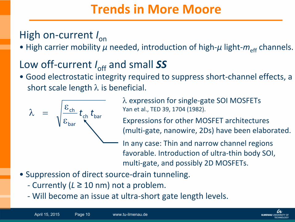
Trends in More Moore
barchbar
ch tt
expression
for
single‐gate
SOI MOSFETs
Yan
et al., TED 39, 1704 (1982).
Expressions
for
other
MOSFET architectures (multi‐gate, nanowire, 2Ds) have
been
elaborated.
In any
case: Thin
and narrow
channel
regions favorable. Introduction
of ultra‐thin
body
SOI,
multi‐gate, and possibly
2D MOSFETs.
April 15, 2015 www.tu-ilmenau.dePage 11
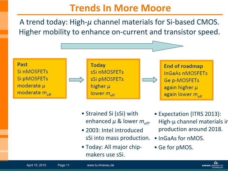
Trends In More Moore
•
Strained
Si (sSi) with enhanced
µ
& lower
meff
.
•
2003: Intel introduced sSi into mass production.
•
Today: All major
chip‐ makers
use sSi.
•
Expectation
(ITRS 2013): High‐µ
channel
materials
in
production
around
2018.
•
InGaAs
for
nMOS.
•
Ge for
pMOS.
A trend
today: High‐µ
channel
materials
for
Si‐based
CMOS.Higher
mobility
to enhance
on‐current
and transistor
speed.
April 15, 2015 www.tu-ilmenau.dePage 12
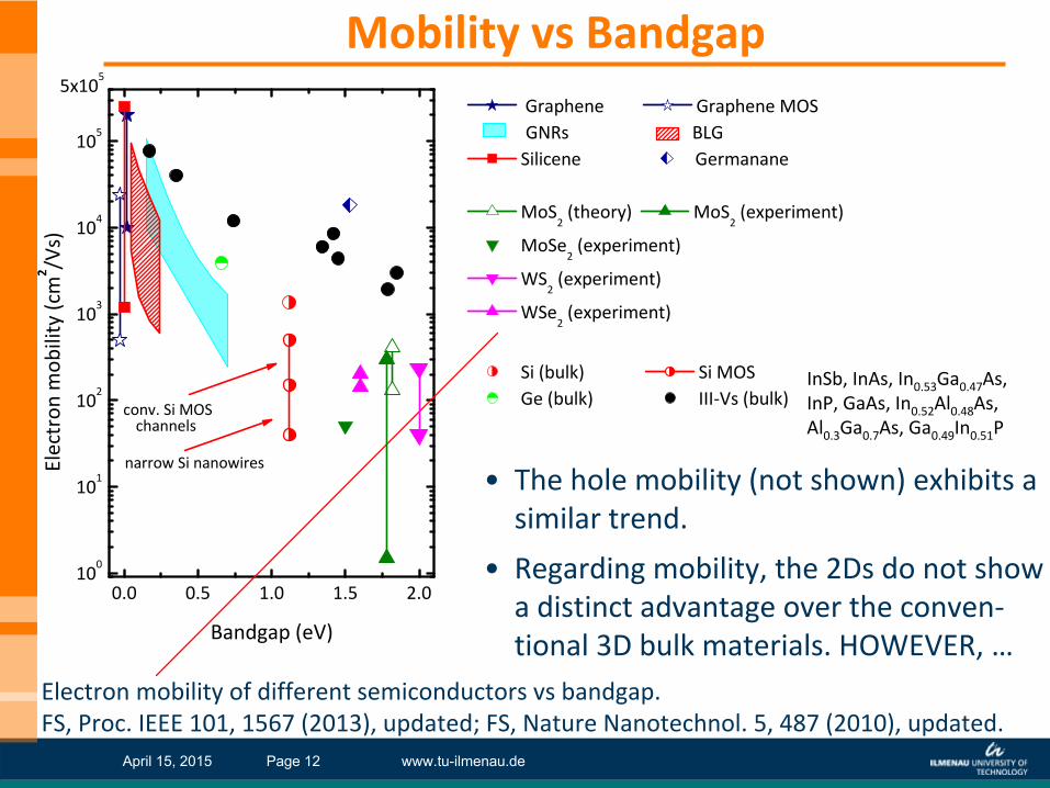
0.0 0.5 1.0 1.5 2.010
0
101
102
103
104
105
narrow Si nanowires
channels
Electron
mob
ility (cm
2 /Vs)
Bandgap (eV)
Graphene Graphene MOS GNRs BLG
Silicene Germanane
MoS2 (theory) MoS
2 (experiment)
MoSe2 (experiment)
WS2 (experiment)
WSe2 (experiment)
Si (bulk) Si MOS Ge (bulk) III‐Vs (bulk)
5x10⁵
conv. Si MOS
Mobility vs Bandgap
•
The
hole mobility (not shown) exhibits a similar trend.
•
Regarding mobility, the 2Ds do not show a distinct advantage over the conven‐
tional 3D bulk materials. HOWEVER, …Electron mobility of different semiconductors vs bandgap.FS, Proc. IEEE 101, 1567 (2013), updated; FS, Nature Nanotechnol. 5, 487 (2010), updated.
InSb, InAs, In0.53
Ga0.47
As, InP, GaAs, In0.52
Al0.48
As,
Al0.3
Ga0.7
As, Ga0.49
In0.51
P
April 15, 2015 www.tu-ilmenau.dePage 13
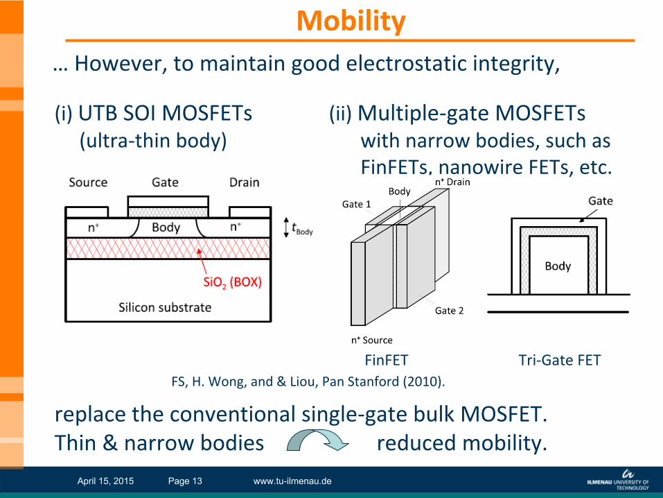
(i) UTB SOI MOSFETs (ii) Multiple‐gate MOSFETs
(ultra‐thin body)
with narrow bodies, such asFinFETs, nanowire FETs, etc.
replace the conventional single‐gate bulk MOSFET. Thin & narrow bodies
reduced mobility.
Mobility… However, to maintain good electrostatic integrity,
FinFET Tri‐Gate
FET
FS, H. Wong, and & Liou, Pan Stanford (2010).

April 15, 2015 www.tu-ilmenau.dePage 14
Mobility
Severely
degraded
electron
mobility
in small‐diameter
Si nanowires.
The
picture
gets
less
cloudy
for
the
2Ds. The
2Ds are
by
nature ultimately
thin.
Granzner, Polyakov,Schippel
& FS, IEEE TED 61, 3601 (2014).

April 15, 2015 www.tu-ilmenau.dePage 15
A View Beyond the ITRS Horizon
• How far can the MOSFET be scaled? Unclear at present.Many
problems: ‐
Degraded electrostatics, degraded switch‐off.‐
Variability and processing
issues
‐
Economic
issues, cost.
• We remember: The 2013 edition
of the
ITRS requires5‐nm gate
MOSFETs
for
the
year
2028.
• One could
say
“5‐nm MOSFETs
–
this
is
wishful
thinking“, BUT thesame
has been
said
about
30‐nm MOSFETs
20 years
ago.
IBM paper
at IEDM 1992.Note: In 1992, 500‐nm
single‐gate
MOSFETs have
been
in production.
• Production‐stage
5‐nm CMOS should
not
be
ruled
out. Let
us
beoptimistic
and assume
the
MOSFET can
be
scaled
to sub‐5‐nm.
April 15, 2015 www.tu-ilmenau.dePage 16
A View
Beyond
the
ITRS HorizonMeanwhile
several
theoretical
studies
on 5‐nm gate
MOSFETs:
‐
Luisier
et al., IEDM, 251 (2011).‐
Alam
& Lake, IEEE TED 59, 3250 (2012).
‐
Sylvia et al., IEEE TED 59 2064 (2012).‐
Mehrotra
et al., IEEE TED 60, 2171 (2013).
‐
Luisier
& Szabo, ULIS, 53 (2013).
‐
etc.
• Consistent
conclusion: At 5‐nm and below
gate
lengthslevels, source‐drain
tunneling
will become
an issue.
• Tunneling degraded
SS
and switch‐off, high Ioff
.
• High‐µ, i.e., light‐meff
narrow‐gap
channel
materials
areexpected
to fail.
• Heavy‐meff
materials
(with
lower
µ
and wider gap) areexpected
to become
favorable.
April 15, 2015 www.tu-ilmenau.dePage 17
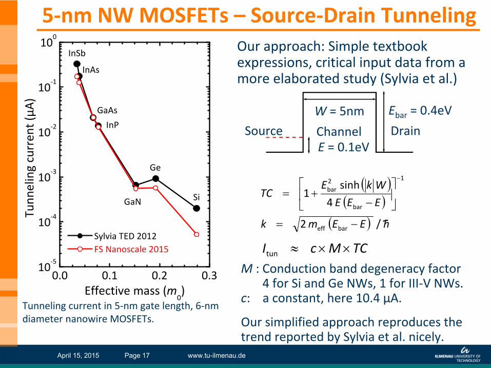
E
= 0.1eVSource Channel Drain
W = 5nm Ebar
= 0.4eV
5‐nm NW MOSFETs
–
Source‐Drain
TunnelingOur approach: Simple textbook
expressions, critical input data from a more elaborated study (Sylvia et al.)
hEEmk
EEE
WkETC
/2
4
sinh1
bareff
1
bar
2bar
Our simplified approach reproduces the trend reported by Sylvia et al. nicely.
TCMcI tun
M : Conduction
band degeneracy
factor4 for
Si and Ge NWs, 1 for
III‐V NWs.
c: a constant, here
10.4 µA.
0.0 0.1 0.2 0.310
‐5
10‐4
10‐3
10‐2
10‐1
100
Si
Ge
GaN
InP
GaAs
InAs
Tunn
eling curren
t (µA
)
Effective mass (m0)
Sylvia TED 2012 FS Nanoscale 2015
InSb
Tunneling current in 5‐nm gate length, 6‐nm
diameter nanowire
MOSFETs.

April 15, 2015 www.tu-ilmenau.dePage 18
0.0 0.2 0.4 0.6 0.8 1.010
‐12
10‐10
10‐8
10‐6
10‐4
10‐2
100
Ge
Si
GaAs
InSb, InAs
MoS2, MoSe
2, MoTe
2
GNR 5 nm
GNR 0.739 nmNW (i)
Transm
ission
coe
fficient
Effective mass (m0)
6‐nm diam. NWs 3.8‐nm diam. Si NWs W‐based 2D TMDs Mo‐based 2D TMDs GNRs
NW (ii)
WS2, WSe
2, WTe
2
5‐nm MOSFETs – Source‐Drain Tunneling
NW(i): <110> Si, 3 GPa compressive strain.
NW(ii): <100> Si, 2 GPa compressive strain.
Si
remains a strongcontender!
A possible
scenario for the selection of MOSFET channel materials.
meff
for 3.8‐nm Si NWs: Mehrotra
et al., TED 60, 2171 (2013).
April 15, 2015 www.tu-ilmenau.dePage 19
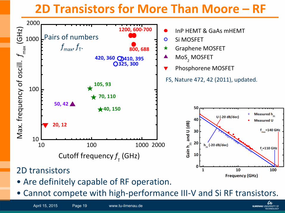
10 100 100010
100
1000
2000
20, 12
50, 42
325, 300
1200, 600‐700
70, 110
410, 395
InP HEMT & GaAs mHEMT Si MOSFET Graphene MOSFET MoS
2 MOSFET
Phosphorene MOSFET
Max. frequ
ency of o
scill. f m
ax (G
Hz)
Cutoff frequency fT (GHz)
800, 688
420, 360
105, 93
40, 150
2000
2D Transistors for
More
Than
Moore – RF
Pairs of numbersfmax
, fT
.
2D
transistors • Are definitely capable of RF operation.• Cannot
compete with high‐performance III‐V and Si
RF transistors.
FS, Nature 472, 42 (2011), updated.

April 15, 2015 www.tu-ilmenau.dePage 20
Flexible Graphene
FETsAkinwande
et al., Nat. Comm. 5, 5678 (2014).
2D Transistors for
More
Than
Moore – Flexible
Promising:
•
Flexible Graphene
FETs
for RF
•
Flexible TMD FETs
for digital logic and RF
Applications for flexible electronicsAkinwande
et al., Nat. Comm. 5, 5678 (2014).
April 15, 2015 www.tu-ilmenau.dePage 21
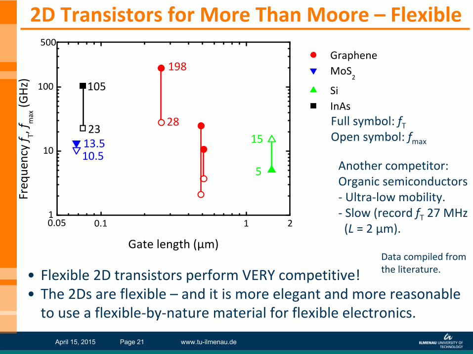
0.1 11
10
100
510.5
2328
20.05
Freq
uency f T, f
max (G
Hz)
Gate length (µm)
Graphene MoS
2
Si InAs
500
198
105
13.5 15
•
Flexible 2D transistors perform VERY competitive!•
The 2Ds are flexible – and it is more elegant and more reasonable
to use a flexible‐by‐nature material for flexible electronics.
2D Transistors for
More
Than
Moore – Flexible
Another competitor: Organic semiconductors
‐ Ultra‐low mobility.‐ Slow (record fT
27 MHz (L
= 2 µm).
Data compiled fromthe literature.
Full symbol: fTOpen symbol: fmax

April 15, 2015 www.tu-ilmenau.dePage 22
Metrology
Needs
for
2D Electronics
•
Analysis of crystallographic structure of 2D layers (at atomic level).
•
Identification of the layer number of 2D sheets.
•
Accurate measurement of width, edge configuration, and bandgap
of narrow GNRs.
•
Correct extraction of the mobility of top‐gated 2D MOS channels.
•
Analysis of the properties of contacts metal – 2D materials (contact type, i.e., Schottky
or Ohmic, contact resistance).
•
Measurement of heat transport properties of 2D materials: thermal conductivity and thermal boundary resistance (between 2D materials
and the substrate/insulator underneath).
Processing 2D transistors and circuits (with the exception of starting material preparation) is based on the well‐established Si
technology.
Thus, many metrology needs for 2D electronics are the same as those for Si
technolgy. There are, however, several additional needs, such as

April 15, 2015 www.tu-ilmenau.dePage 23
0.1 1 10 10010
0
101
102
103
104
N = 7, i.e., ac 3p+1
experiment lithography experiment synthesis theory ac theory zz
ac 3p+2ac 3p
ac 3p+1
Ba
ndgap (m
eV)
Width (nm)
Metrology
Needs
–
GNR Gap vs Width
GNR bandgap
vs width.
FS, Pezoldt, Granzner,
Nanoscale
2015.
The bandgap of GNRs
depends strongly on the ribbon width and the edge configuration!
April 15, 2015 www.tu-ilmenau.dePage 24
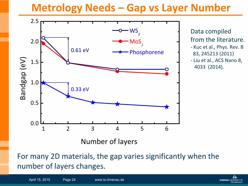
1 2 3 4 5 60.0
0.5
1.0
1.5
2.0
2.5
0.33 eV
Band
gap (eV)
Number of layers
WS2
MoS2
Phosphorene0.61 eV
Metrology
Needs
–
Gap
vs
Layer
Number
For many 2D materials, the gap varies significantly when the number of layers changes.
Data compiled from the literature.
‐ Kuc
et al., Phys. Rev. B 83, 245213 (2011)‐ Liu et al., ACS Nano
8, 4033 (2014).

April 15, 2015 www.tu-ilmenau.dePage 25
• The
2D materials
are
DEFINITELY promising
for
many
applications.
• 2D MOSFETs
for
More
Moore
‐
No significant
impact
expected
in the
near
to medium
term, i.e., within
the
current
ITRS horizon
(L
> 5 nm).
‐
Potential beyond
the
ITRS horizon
(L
≤
5 nm)‐
2Ds offer
short
scale
length
and excellent
electrostatics.
‐
TMD and GNR MOSFETs: Efficient
suppression
of direct source‐drain
tunneling).
• 2D MOSFETs
for
More
Than
Moore
‐
Promising
(already
in the
near
to medium
term) forflexible electronics, both
digital and analog/RF.
‐
2Ds promising
for
printable
and transparent electronics.
Conclusion

April 15, 2015 www.tu-ilmenau.dePage 26
Metrology
Needs
• Many of the metrology needs for 2D electronics are the same asfor Si
technolgy.
• There are, however, several additional needs regarding‐
Crystallographic structure of 2D layers at the atomic
level.
‐
Layer number of 2D sheets.‐
Width, edge configuration, and bandgap
of narrow GNRs.
‐
Mobility of top‐gated 2D MOS channels. ‐
Properties of contacts metal – 2D materials (contact type,
‐
Heat transport properties.
AcknowledgementThis
work
was/is
supported
by
DFG Priority
Program
SPP 1459 Graphene
and TU Ilmenau
University Excellence
Research Grants.
Conclusion