2864 IEEE TRANSACTIONS ON NUCLEAR SCIENCE, …padley.rice.edu/cms/05280502.pdf · 2864 IEEE...
10
2864 IEEE TRANSACTIONS ON NUCLEAR SCIENCE, VOL. 56, NO. 5, OCTOBER 2009 High-Speed, Fixed-Latency Serial Links With FPGAs for Synchronous Transfers Alberto Aloisio, Francesco Cevenini, Raffaele Giordano, and Vincenzo Izzo Abstract—Fixed-latency serial links find application in trigger and data acquisition systems of High Energy Physics (HEP) exper- iments requiring a predictable data transfer timing. In some archi- tectures, there is the need to clock the data in and out from the link synchronously with a system clock (i.e., synchronous transfers) in- stead of using the clock recovered from the serial stream. In this work, we present a synchronous link architecture based on high-speed transceivers embedded in latest generation Field Programmable Gate Arrays (FPGAs). These transceivers are typically designed for applications that tolerate latency variations. However, we have developed two configurations and a clocking scheme to implement fixed-latency operation. The latency is constant during the transfer, after a loss of lock or a power cycle. Once locked, the link can be considered as a synchronous pipeline. The configurations do not depend on a particular serial encoding, the encoder/decoder being external to the transceiver. We discuss the latency performance for each configuration and show an implementation of the architecture we propose. We also present experimental results showing the stability of the latency of the link. Index Terms—Data acquisition, FPGAs, latency, serial links, synchronous transfers. I. INTRODUCTION H IGH-SPEED transceivers embedded in FPGAs are typically designed for applications that do not re- quire a deterministic latency with an accuracy at the level of nanosecond. Nevertheless, within the HEP community, some attempts have been made in order to take advantage of these devices in the design of fixed-latency links, due to the obvious benefits in terms of system integration, power dissipation and cost. We now briefly summarize and comment some results obtained in the field of FPGA-based serial links for application to HEP. A study [1] have been conducted about the possibility to im- plement serial links of Large Hadron Collider (LHC) experi- ments by means of FPGA-embedded serial transceivers. The study focused on Multi-Gigabit Transceivers (MGTs) [2] em- bedded in Xilinx Virtex-II Pro devices and led to the imple- mentation of a variable latency link compatible with a radia- Manuscript received December 22, 2008; revised April 09, 2009. Current ver- sion published October 07, 2009. This work was supported in part as a Pro- gramma di Ricerca di rilevante Interesse Nazionale (PRIN) by the Italian Min- istero dell’Istruzione, Università e Ricerca Scientifica. The authors are with the INFN Sezione di Napoli and Università degli Studi di Napoli “Federico II”, Dipartimento di Scienze Fisiche, 80126 Napoli, Italy (e-mail: [email protected]; [email protected]; [email protected]; [email protected]). Color versions of one or more of the figures in this paper are available online at http://ieeexplore.ieee.org. Digital Object Identifier 10.1109/TNS.2009.2027236 tion-hard serializer [3] developed at CERN. In the framework of the A Large Ion Collider Experiment (ALICE), a Conditional Inversion Master Transition (CIMT) [4] compliant deserializer [5] based on Xilinx and Altera embedded SerDes has been de- signed. The Altera version has been experimentally tested, while the Xilinx one has only been simulated. Both solutions have been discarded because the latency of link was too high for the application. Moreover, the latency of the deserializer resulted to be variable. Another CIMT receiver has been implement by means of latest Xilinx transceivers for a portable test system [6] of a sub-detector of the A Toroidal LHC AapparatuS (ATLAS) experiment. No details about the latency of the implementa- tion are provided and it is unclear whether or not the transfer is synchronous. The Compact Muon Solenoid (CMS) experi- ment’s Global Calorimeter Trigger (GCT) includes some serial links [7] based on Xilinx MGTs. The links perform fixed-la- tency data transfers, unfortunately the authors do not provide details of the architecture and do not specify if the latency is al- ways the same at each power-up of the link. The Level-0 muon trigger of the Large Hadron Collider beauty (LHCb) experiment [8] strongly relies on multi-Gigabit 8b10b serial links imple- mented with Altera embedded SerDes. Unfortunately, no details about the latency of the links are available. The Gigabit Trans- ceiver project [9], currently under development at CERN, aims at providing a radiation-tolerant SerDes for trigger and data ac- quisition applications to super Large Hadron Collider (sLHC) experiments. The project foresees the deployment of FPGA-em- bedded SerDes on the off-detector part of the link. Trigger trans- fers will require a fixed-latency configuration of the SerDes. All the cited papers mainly focus on the application of the developed links to the pertaining experiment but do not provide details on the system architectures. In order to bridge this gap, we present here a fixed-latency architecture based on a config- urable SerDes embedded in a latest-generation FPGA device. We studied its architecture in order to find a configuration and a clocking scheme to achieve a deterministic transmission delay in synchronous transfers. As a case study for the discussion of our architecture, we choose the implementation of a serial link to be deployed in the ATLAS experiment. In the barrel section of the ATLAS muon spectrometer [10], Level 1 (L1) trigger data is transferred across optical fibers from the on-detector electronics to the readout system, which is hosted in a counting room, at about a hundred meters from the detector. The transmitter electronics consists of custom boards, while the receiving ones lie in VME crates. The whole data path is implemented as a synchronous pipeline clocked by the Timing, Trigger and Control (TTC) system [11]. It distributes timing information such as the bunch crossing clock 0018-9499/$26.00 © 2009 IEEE
Transcript of 2864 IEEE TRANSACTIONS ON NUCLEAR SCIENCE, …padley.rice.edu/cms/05280502.pdf · 2864 IEEE...

2864 IEEE TRANSACTIONS ON NUCLEAR SCIENCE, VOL. 56, NO. 5, OCTOBER 2009
High-Speed, Fixed-Latency Serial LinksWith FPGAs for Synchronous Transfers
Alberto Aloisio, Francesco Cevenini, Raffaele Giordano, and Vincenzo Izzo
Abstract—Fixed-latency serial links find application in triggerand data acquisition systems of High Energy Physics (HEP) exper-iments requiring a predictable data transfer timing. In some archi-tectures, there is the need to clock the data in and out from the linksynchronously with a system clock (i.e., synchronous transfers) in-stead of using the clock recovered from the serial stream.
In this work, we present a synchronous link architecture basedon high-speed transceivers embedded in latest generation FieldProgrammable Gate Arrays (FPGAs). These transceivers aretypically designed for applications that tolerate latency variations.However, we have developed two configurations and a clockingscheme to implement fixed-latency operation. The latency isconstant during the transfer, after a loss of lock or a power cycle.Once locked, the link can be considered as a synchronous pipeline.The configurations do not depend on a particular serial encoding,the encoder/decoder being external to the transceiver. We discussthe latency performance for each configuration and show animplementation of the architecture we propose. We also presentexperimental results showing the stability of the latency of thelink.
Index Terms—Data acquisition, FPGAs, latency, serial links,synchronous transfers.
I. INTRODUCTION
H IGH-SPEED transceivers embedded in FPGAs aretypically designed for applications that do not re-
quire a deterministic latency with an accuracy at the level ofnanosecond. Nevertheless, within the HEP community, someattempts have been made in order to take advantage of thesedevices in the design of fixed-latency links, due to the obviousbenefits in terms of system integration, power dissipation andcost. We now briefly summarize and comment some resultsobtained in the field of FPGA-based serial links for applicationto HEP.
A study [1] have been conducted about the possibility to im-plement serial links of Large Hadron Collider (LHC) experi-ments by means of FPGA-embedded serial transceivers. Thestudy focused on Multi-Gigabit Transceivers (MGTs) [2] em-bedded in Xilinx Virtex-II Pro devices and led to the imple-mentation of a variable latency link compatible with a radia-
Manuscript received December 22, 2008; revised April 09, 2009. Current ver-sion published October 07, 2009. This work was supported in part as a Pro-gramma di Ricerca di rilevante Interesse Nazionale (PRIN) by the Italian Min-istero dell’Istruzione, Università e Ricerca Scientifica.
The authors are with the INFN Sezione di Napoli and Università degliStudi di Napoli “Federico II”, Dipartimento di Scienze Fisiche, 80126 Napoli,Italy (e-mail: [email protected]; [email protected]; [email protected];[email protected]).
Color versions of one or more of the figures in this paper are available onlineat http://ieeexplore.ieee.org.
Digital Object Identifier 10.1109/TNS.2009.2027236
tion-hard serializer [3] developed at CERN. In the frameworkof the A Large Ion Collider Experiment (ALICE), a ConditionalInversion Master Transition (CIMT) [4] compliant deserializer[5] based on Xilinx and Altera embedded SerDes has been de-signed. The Altera version has been experimentally tested, whilethe Xilinx one has only been simulated. Both solutions havebeen discarded because the latency of link was too high for theapplication. Moreover, the latency of the deserializer resultedto be variable. Another CIMT receiver has been implement bymeans of latest Xilinx transceivers for a portable test system [6]of a sub-detector of the A Toroidal LHC AapparatuS (ATLAS)experiment. No details about the latency of the implementa-tion are provided and it is unclear whether or not the transferis synchronous. The Compact Muon Solenoid (CMS) experi-ment’s Global Calorimeter Trigger (GCT) includes some seriallinks [7] based on Xilinx MGTs. The links perform fixed-la-tency data transfers, unfortunately the authors do not providedetails of the architecture and do not specify if the latency is al-ways the same at each power-up of the link. The Level-0 muontrigger of the Large Hadron Collider beauty (LHCb) experiment[8] strongly relies on multi-Gigabit 8b10b serial links imple-mented with Altera embedded SerDes. Unfortunately, no detailsabout the latency of the links are available. The Gigabit Trans-ceiver project [9], currently under development at CERN, aimsat providing a radiation-tolerant SerDes for trigger and data ac-quisition applications to super Large Hadron Collider (sLHC)experiments. The project foresees the deployment of FPGA-em-bedded SerDes on the off-detector part of the link. Trigger trans-fers will require a fixed-latency configuration of the SerDes.
All the cited papers mainly focus on the application of thedeveloped links to the pertaining experiment but do not providedetails on the system architectures. In order to bridge this gap,we present here a fixed-latency architecture based on a config-urable SerDes embedded in a latest-generation FPGA device.We studied its architecture in order to find a configuration and aclocking scheme to achieve a deterministic transmission delayin synchronous transfers. As a case study for the discussion ofour architecture, we choose the implementation of a serial linkto be deployed in the ATLAS experiment.
In the barrel section of the ATLAS muon spectrometer [10],Level 1 (L1) trigger data is transferred across optical fibersfrom the on-detector electronics to the readout system, whichis hosted in a counting room, at about a hundred meters fromthe detector. The transmitter electronics consists of customboards, while the receiving ones lie in VME crates. The wholedata path is implemented as a synchronous pipeline clockedby the Timing, Trigger and Control (TTC) system [11]. Itdistributes timing information such as the bunch crossing clock
0018-9499/$26.00 © 2009 IEEE
ALOISIO et al.: HIGH-SPEED, FIXED-LATENCY SERIAL LINKS WITH FPGAS FOR SYNCHRONOUS TRANSFERS 2865
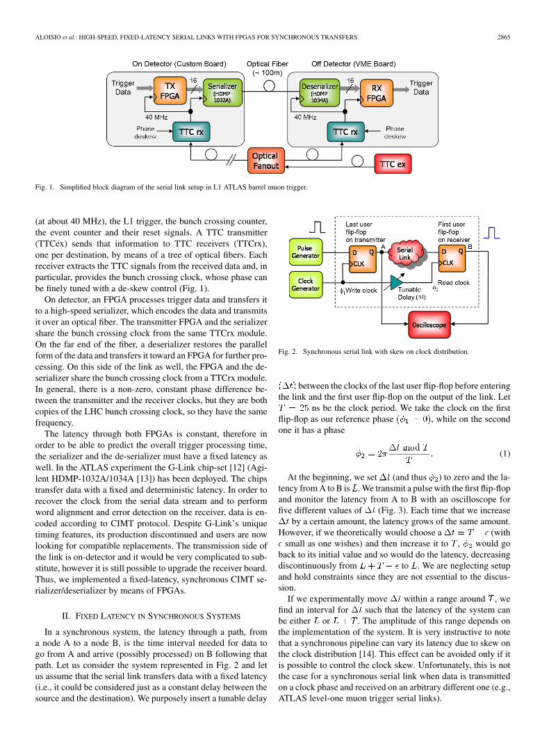
Fig. 1. Simplified block diagram of the serial link setup in L1 ATLAS barrel muon trigger.
(at about 40 MHz), the L1 trigger, the bunch crossing counter,the event counter and their reset signals. A TTC transmitter(TTCex) sends that information to TTC receivers (TTCrx),one per destination, by means of a tree of optical fibers. Eachreceiver extracts the TTC signals from the received data and, inparticular, provides the bunch crossing clock, whose phase canbe finely tuned with a de-skew control (Fig. 1).
On detector, an FPGA processes trigger data and transfers itto a high-speed serializer, which encodes the data and transmitsit over an optical fiber. The transmitter FPGA and the serializershare the bunch crossing clock from the same TTCrx module.On the far end of the fiber, a deserializer restores the parallelform of the data and transfers it toward an FPGA for further pro-cessing. On this side of the link as well, the FPGA and the de-serializer share the bunch crossing clock from a TTCrx module.In general, there is a non-zero, constant phase difference be-tween the transmitter and the receiver clocks, but they are bothcopies of the LHC bunch crossing clock, so they have the samefrequency.
The latency through both FPGAs is constant, therefore inorder to be able to predict the overall trigger processing time,the serializer and the de-serializer must have a fixed latency aswell. In the ATLAS experiment the G-Link chip-set [12] (Agi-lent HDMP-1032A/1034A [13]) has been deployed. The chipstransfer data with a fixed and deterministic latency. In order torecover the clock from the serial data stream and to performword alignment and error detection on the receiver, data is en-coded according to CIMT protocol. Despite G-Link’s uniquetiming features, its production discontinued and users are nowlooking for compatible replacements. The transmission side ofthe link is on-detector and it would be very complicated to sub-stitute, however it is still possible to upgrade the receiver board.Thus, we implemented a fixed-latency, synchronous CIMT se-rializer/deserializer by means of FPGAs.
II. FIXED LATENCY IN SYNCHRONOUS SYSTEMS
In a synchronous system, the latency through a path, froma node A to a node B, is the time interval needed for data togo from A and arrive (possibly processed) on B following thatpath. Let us consider the system represented in Fig. 2 and letus assume that the serial link transfers data with a fixed latency(i.e., it could be considered just as a constant delay between thesource and the destination). We purposely insert a tunable delay
Fig. 2. Synchronous serial link with skew on clock distribution.
between the clocks of the last user flip-flop before enteringthe link and the first user flip-flop on the output of the link. Let
ns be the clock period. We take the clock on the firstflip-flop as our reference phase , while on the secondone it has a phase
(1)
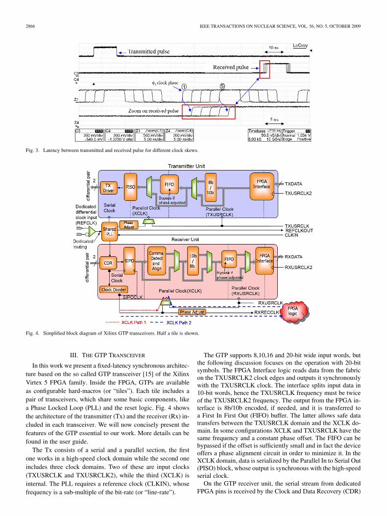
At the beginning, we set (and thus ) to zero and the la-tency from A to B is . We transmit a pulse with the first flip-flopand monitor the latency from A to B with an oscilloscope forfive different values of (Fig. 3). Each time that we increase
by a certain amount, the latency grows of the same amount.However, if we theoretically would choose a (with
small as one wishes) and then increase it to , would goback to its initial value and so would do the latency, decreasingdiscontinuously from to . We are neglecting setupand hold constraints since they are not essential to the discus-sion.
If we experimentally move within a range around , wefind an interval for such that the latency of the system canbe either or . The amplitude of this range depends onthe implementation of the system. It is very instructive to notethat a synchronous pipeline can vary its latency due to skew onthe clock distribution [14]. This effect can be avoided only if itis possible to control the clock skew. Unfortunately, this is notthe case for a synchronous serial link when data is transmittedon a clock phase and received on an arbitrary different one (e.g.,ATLAS level-one muon trigger serial links).
2866 IEEE TRANSACTIONS ON NUCLEAR SCIENCE, VOL. 56, NO. 5, OCTOBER 2009
Fig. 3. Latency between transmitted and received pulse for different clock skews.
Fig. 4. Simplified block diagram of Xilinx GTP transceivers. Half a tile is shown.
III. THE GTP TRANSCEIVER
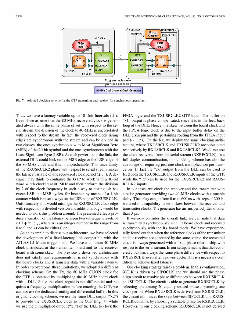
In this work we present a fixed-latency synchronous architec-ture based on the so called GTP transceiver [15] of the XilinxVirtex 5 FPGA family. Inside the FPGA, GTPs are availableas configurable hard-macros (or “tiles”). Each tile includes apair of transceivers, which share some basic components, likea Phase Locked Loop (PLL) and the reset logic. Fig. 4 showsthe architecture of the transmitter (Tx) and the receiver (Rx) in-cluded in each transceiver. We will now concisely present thefeatures of the GTP essential to our work. More details can befound in the user guide.
The Tx consists of a serial and a parallel section, the firstone works in a high-speed clock domain while the second oneincludes three clock domains. Two of these are input clocks(TXUSRCLK and TXUSRCLK2), while the third (XCLK) isinternal. The PLL requires a reference clock (CLKIN), whosefrequency is a sub-multiple of the bit-rate (or “line-rate”).
The GTP supports 8,10,16 and 20-bit wide input words, butthe following discussion focuses on the operation with 20-bitsymbols. The FPGA Interface logic reads data from the fabricon the TXUSRCLK2 clock edges and outputs it synchronouslywith the TXUSRCLK clock. The interface splits input data in10-bit words, hence the TXUSRCLK frequency must be twiceof the TXUSRCLK2 frequency. The output from the FPGA in-terface is 8b/10b encoded, if needed, and it is transferred toa First In First Out (FIFO) buffer. The latter allows safe datatransfers between the TXUSRCLK domain and the XCLK do-main. In some configurations XCLK and TXUSRCLK have thesame frequency and a constant phase offset. The FIFO can bebypassed if the offset is sufficiently small and in fact the deviceoffers a phase alignment circuit in order to minimize it. In theXCLK domain, data is serialized by the Parallel In to Serial Out(PISO) block, whose output is synchronous with the high-speedserial clock.
On the GTP receiver unit, the serial stream from dedicatedFPGA pins is received by the Clock and Data Recovery (CDR)

ALOISIO et al.: HIGH-SPEED, FIXED-LATENCY SERIAL LINKS WITH FPGAS FOR SYNCHRONOUS TRANSFERS 2867
Fig. 5. Recommended GTP clocking scheme when using phase alignment circuits.
circuit, which extracts a clock and uses it to sample the data. Theextracted clock is divided to generate a recovered clock for theSerial In to Parallel Output (SIPO), SIPOCLK and one for theparallel section (RXRECCLK), which can be used to clock thereceiving FPGA logic. The SIPO block de-serializes data into10-bit words synchronously with SIPOCLK, which can have aphase difference with respect to RXRECCLK. The next blockin the data-path works synchronously with XCLK, which canbe driven by SIPOCLK (XCLK path 1 in Fig. 4) or RXUS-RCLK. In the latter case, there is a clock domain crossing fromSIPOCLK to RXUSRCLK and it must be resolved. If RXUS-RCLK is derived from RXRECCLK (XCLK path 2 in Fig. 4),there is in general a phase offset due to the path in FPGA fabricclocking elements (buffers, routing, PLLs, etc.). In this case, it ispossible to minimize the offset between SIPOCLK and RXUS-RCLK, by means of a dedicated phase alignment circuit. TheComma Detect and Align block following the SIPO can be pro-grammed to search for and align to a comma. If alignment isperformed outside of the GTP, this block can be skipped. Datais 10b to 8b decoded, if needed, and transferred to a FIFO inorder to enter the RXUSRCLK domain (when XCLK is drivenby SIPOCLK, otherwise data is already in the RXUSRCLK do-main). The FPGA interface combines 10-bit words from theRXUSRCLK domain and outputs 20-bit words in the RXUS-RCLK2 domain at half of the frequency.
IV. FIXED-LATENCY GTP CONFIGURATIONS
Unfortunately, standard GTP configurations do not have fixedlatency. Moreover, we would like to keep the latency of the linkas low as possible. We begin by discussing the configurationsuggested by the vendor and analyzing its weaknesses. After-ward, we introduce our solution.
Let us suppose we need to implement an 800 Mb/s transmis-sion of 20-bit frames. The minimum clock frequency requiredby the GTP for the reference clock is 60 MHz, so we choose80-MHz clock sources. Since we want to achieve a latency aslow as possible we bypass the GTP Tx and Rx FIFO and usetheir phase align circuits instead. The FPGA logic on both thelink sides is in charge of activating the phase alignment cir-cuits, by means of the TXPHASE and RXPHASE signals, andchecking if the alignment has been achieved. Under these con-ditions, the clocking scheme suggested by the vendor is the fol-lowing (Fig. 5).
Fig. 6. Timing diagram of the generation of the recovered clock.
On both the Tx and Rx, the CLKIN input of the GTP receivesan 80 MHz clock by means of the dedicated GTP differentialclock buffer and routing.
On the Tx side, a Delay Locked Loop (DLL) divides the RE-FCLKOUT (at 80 MHz) from the GTP to generate a 40 MHzclock for the TXUSRCLK2 input and the FPGA logic. The un-divided output of the DLL (“ ”) is used to feed the TXUS-RCLK input of the GTP. According to the User Guide, TXUS-RCLK and TXUSRCLK2 must be positive edge aligned withas low skew as possible. The clock buffer delay on the DLL“ ” output is compensated since it is inserted in the feedbackloop. The other clock buffer can be considered compensated aslong as buffer delays can be considered identical. Under this ap-proximation, TXUSRCLK and TXUSRCLK2 are positive-edgealigned with no skew.
On the Rx side, a DLL divides the clock recovered from theserial stream (RXRECCLK at 80 MHz) to generate the RXUS-RCLK2 clock (at 40 MHz) for the GTP and the FPGA logic.The undivided output from the DLL is used to produce RXUS-RCLK with no skew with respect to RXUSRCLK2, as requiredby the GTP specifications.
The described clocking strategy is iso-synchronous, becausethe GTPs generate the clocks for the transmitting and receivingFPGA logic. On the Tx side, data enters the GTP synchronouslywith a TXUSRCLK2 generated from the REFCLKOUT clock,which may have a skew with respect to the board clock drivingthe GTP PLL (CLKIN). On the Rx, data exits from the GTPsynchronously with the RXUSRCLK2 clock generated from therecovered clock (RXRECCLK), whose phase and frequency de-pend on the incoming serial stream and not on the board clock.This clocking strategy does not allow us to clock data in and outfrom the link synchronously with the board clocks.
Let us now focus on the latency of the transmission. Edgesin the serial stream can be divided in 10 classes, each labeledby a bit position in a 10-bit symbol (Fig. 6) (#0, #1…, #9).At each power-up, the GTP can randomly produce a recoveredclock aligned with edges belonging to one of the 10 classes.
2868 IEEE TRANSACTIONS ON NUCLEAR SCIENCE, VOL. 56, NO. 5, OCTOBER 2009
Fig. 7. Adopted clocking scheme for the GTP transmitter and receiver for synchronous operation.
Thus, we have a latency variable up to 10 Unit Intervals (UI).Even if we assume that the 80-MHz recovered clock is gener-ated always with the same phase offset with respect to the se-rial stream, the division of the clock to 40-MHz is uncorrelatedwith respect to the stream. In fact, the recovered clock risingedges are synchronous with the stream and can be divided intwo classes: the ones synchronous with Most Significant Byte(MSB) of the 20-bit symbol and the ones synchronous with theLeast Significant Byte (LSB). At each power-up of the link, theexternal DLL could lock on the MSB edge or the LSB edge ofthe 80-MHz clock and this is unpredictable. This uncertaintyof the RXUSRCLK2 phase with respect to serial stream makesthe latency variable of one recovered clock period . A de-signer may think to configure the GTP to work with a 10-bitword width clocked at 80 MHz and then perform the divisionby 2 of the clock frequency in such a way to distinguish be-tween LSB and MSB cycles, for instance by means of a 1-bitcounter which is reset always on the LSB edge of RXUSRCLK.Unfortunately, this would misalign the RXUSRCLK clock edgewith respect to its divided version and additional logic would beneeded to work this problem around. The presented effects pro-duce a variation of the latency between two subsequent resets of
, where is an integer number in the range from0 to 9 and can be either 0 or 1.
As an example to discuss our architecture, we have selectedthe development of a fixed-latency link compatible with theATLAS L1 Muon trigger links. We have a common 40-MHzclock distributed at the transmitter board and to the receiverboard with some skew. The previously described architecturedoes not satisfy our requirements: it is not synchronous withthe board clocks and it transfers data with a variable latency.In order to overcome these limitations, we adopted a differentclocking scheme. On the Tx, the 80 MHz CLKIN clock forthe GTP is obtained by multiplying the 40 MHz board clockwith a DLL. Since the clock signal is not differential and re-quires a frequency multiplication before entering the GTP, wecan not use the dedicated routing and differential buffer. In thisoriginal clocking scheme, we use the same DLL output (“x2”)to provide the TXUSRCLK clock to the GTP (Fig. 7), whilewe use the unmultiplied output (“x1”) of the DLL to clock the
FPGA logic and the TXUSRCLK2 GTP input. The buffer on“x1” output is phase compensated, since it is in the feed-backloop of the DLL. Hence, the skew between the board clock andthe FPGA logic clock is due to the input buffer delay on theDLL clkin pin and the pertaining routing from the FPGA inputpad ( 1 ns). On the Rx, we deploy the same clocking archi-tecture, where TXUSRCLK and TXUSRCLK2 are substitutedrespectively by RXUSRCLK and RXUSRCLK2. We do not usethe clock recovered from the serial stream (RXRECCLK). In afull-duplex communication, this clocking scheme has also theadvantage of requiring just one clock multiplication per trans-ceiver. In fact the “2x” output from the DLL can be used tofeed both the TXUSRCLK and RXUSRCLK inputs of the GTP,while the “1x” can be used for the TXUSRCLK2 and RXUS-RCLK2 inputs.
In our tests, we clock the receiver and the transmitter witha pulse generator providing two 40-MHz clocks with a tunabledelay. The delay can go from 0 ns to 600 ns with steps of 200 fs;we used this capability to set a skew between the receiver andtransmitter clocks. The generator has an rms period jitter smallerthan 3 ps.
If we now consider the overall link, we can note that datais transmitted synchronously with Tx board clock and receivedsynchronously with the Rx board clock. We have experimen-tally found out that when the reference clocks of the transmitterand the receiver are generated by the same source, the recoveredclock is always generated with a fixed phase relationship withrespect to the serial stream. In our setup, it means that the recov-ered clock has always the same phase difference with respect toRXUSRCLK, even after a power-cycle. This is a necessary con-dition to achieve fixed latency.
Our clocking strategy raises a problem. In this configuration,XCLK is driven by SIPOCLK and we should use the phasealign circuit to resolve phase differences between RXUSRCLKand SIPOCLK. The circuit is able to generate RXRECCLK byselecting one among 20 equally spaced phases, spanning oneclock period. When RXUSRCLK is derived from RXRECCLK,the circuit minimizes the skew between SIPOCLK and RXUS-RCLK domains, by choosing a suitable phase for RXRECCLK.However, in our clocking scheme RXUSRCLK is not derived

ALOISIO et al.: HIGH-SPEED, FIXED-LATENCY SERIAL LINKS WITH FPGAS FOR SYNCHRONOUS TRANSFERS 2869
Fig. 8. Histogram showing the relative phase between RXRECCLK and the reference clock when�� does not satisfy the requirements of the phase align circuit.
from RXRECCLK, thus a phase shift on RXRECCLK has no ef-fect on RXUSRCLK. Let be the phase difference betweenSIPOCLK and RXUSRCLK. If the phase align circuit is acti-vated two situations can happen:
1) satisfies the requirements of the circuit and no phaseshift on RXRECCLK is performed;
2) does not satisfy the requirements of the circuit and thephase of RXRECCLK is changed, but, as this do not affectthe RXUSRCLK phase, the circuit keeps on changing thephase forever.
The histogram of the relative phase between RXRECCLK andthe reference clock (Fig. 8) has been acquired in the secondsituation, and shows all the possible phase offsets.
Thus, a particular RXUSRCLK phase is suitable to readsafely data from the SIPO, if the phase align circuit does notcontinuously shift RXRECCLK. We designed a very simplelogic (the “Phase Checker” block in Fig. 7) which activatesthe phase alignment circuitry and checks whether or not therecovered clock is shifting with respect to RXUSRCLK. IfRXRECCLK is not shifting, this means the RXUSRCLKphase satisfies the requirements of the phase align circuitryand the logic asserts the PHASEOK signal. The phase offsetbetween the transmitter board clock (which is synchronouswith RXRECCLK) and the receiver board clock (which issynchronous with RXUSRCLK) must be set, either inside theFPGA or externally, to a suitable value by checking the levelof the PHASEOK signal. In synchronous applications wherethe relative clock phase can be tuned, this is not an issue. Forinstance in the ATLAS experiment, in order to find a suitablephase difference, the designer may include a dedicated logicin charge of checking the PHASEOK signal and, if needed,changing the clock phase by means of the dedicated TTCrxde-skew feature, which is accessible via a I2C interface.
The described configuration of the GTP, which we will furtherrefer to as “Configuration One”, has the minimum achievablelatency with the GTP. Unfortunately, Configuration One can beused only to transfer 10-bit or 20-bit frames and not 8-bit or16-bit frames, which instead are supported by the GTP whenusing the internal FIFO.
For applications where a phase tuning is not possible, we de-veloped another configuration, which we will refer to as “Con-figuration Two”. We kept the same configuration for the GTPswith the only difference that we enabled the FIFO on the re-ceiver. The FIFO allows to compensate any phase differencebetween the transmission and reception clocks, and the use ofthe phase alignment circuit is not necessary. Data is written inthe FIFO synchronously with SIPOCLK and read with RXUS-RCLK, which are phase misaligned but synchronous. The GTPguarantees that, after a reset, the FIFO is always filled with thesame number of words before starting to output them. This en-sures a deterministic latency through the FIFO. We have set thisvalue to the minimum (3 words), in order to have the lowest pos-sible latency. Configuration Two solves the phase offset issuesencountered with Configuration One and supports all the framewidths offered by the GTP. Unfortunately, the deployment ofthe FIFO increases the latency by 3 RXUSRCLK clock cycles.
The latencies of the transmitter and the receiver in Config-uration One, estimated by means of the user guide, are givenin Table I. For each component we report the latency in termsof RXUSRCLK periods and its absolute value in nanoseconds.We remark that some blocks (e.g., FIFOs) have an associatedlatency even if they are not used. The total latency of the trans-mitter and of the receiver are respectively 4.5 and 9.5 clock pe-riods. In Configuration Two, the latency of the transmitter is still4.5 clock periods, while latency of the receiver is 12.5 clock pe-riods (due to the activation of the FIFO).
V. APPLICABILITY OF THE PROPOSED ARCHITECTURE TO
OTHER EMBEDDED TRANSCEIVERS
Our experience is that the documentation provided by FPGAvendors is not sufficient to predict if fixed-latency operation canbe achieved. We tested in the field the architecture we proposefor the Xilinx GTP transceiver. Configurations of other trans-ceivers should be experimentally tested as well. We now discussthe applicability of our configurations and clocking strategy tolatest FPGA-embedded SerDes produced by Altera and Lattice.We warn the reader that the following discussion is only basedon information found in the data-sheets.

2870 IEEE TRANSACTIONS ON NUCLEAR SCIENCE, VOL. 56, NO. 5, OCTOBER 2009
TABLE ILATENCY OF THE INTERNAL BLOCKS OF THE TRANSMITTER
AND OF THE RECEIVER
GX transceivers [16] embedded in the Altera Stratix IVFPGA family and flexi Physical Coding Sublayer (flexiPCS)transceivers [17] embedded in LatticeSC/M devices offer a sim-pler clocking strategy than the GTP. In fact, they only need thereference clock for the internal PLL plus a transmit clock and areceive clock to interface with the FPGA fabric. All the clocksfor the internal domains are generated by a dedicated circuitryand are hidden to the user. On the contrary, the GTP requiresthe reference clock plus two transmit clocks (TXUSRCLKand TXUSRCLK2) and two receive clocks (RXUSRCLK andRXUSRCLK2).
For both the GX and the flexiPCS it is unspecified if the re-covered clock has fixed phase relationship with respect to theserial stream. Both devices include FIFOs to resolve phase dif-ferences between the internal parallel clock domains and the ex-ternal transmission and reception clock domains. They do notoffer any alternative low-latency configuration, on the contraryof what Xilinx does with the phase alignment circuit. The AlteraGX offer a number of options for skipping internal sub-blocks(FIFOs, 8b10b encoder, etc.) comparable to the Xilinx GTP.Configuration Two could in principle be implemented by skip-ping all the blocks in the data-path but the phase compensationFIFO. However, the latency through the FIFO can vary from 2to 3 clock cycles in the “low-latency mode” and 4 to 5 clockcycles in the “high-latency mode”. It is not specified if, aftera reset, the FIFO is always filled with same number of wordsprior to start transferring them to the fabric. Configuration Oneshould be supported by using the “PMA Direct Drive” modeof the GX, which allows to skip all the blocks in data-path, in-cluding the FIFO. With this device, Configuration One is thebest candidate, among the two, in order to achieve a fixed la-tency, but it should be experimentally tested.
As far as it concerns the flexiPCS, the device offers severalworking modes, each suited to a different protocol. A specialmode, named “SerDes Only” allows the use of an external en-coder. The phase compensation FIFO can not be skipped and itcould possibly prevent a fixed-latency operation. The data-sheet
Fig. 9. Experimental setup for latency tests.
provides no information about the latency through the FIFO, butstates that the latency through the receiver is 5 parallel clockcycles. In this device only Configuration Two could be imple-mented and it is not clear whether or not fixed-latency operationis achievable.
VI. G-LINK EMULATION
The configuration we developed are coding-independent, infact no assumptions have been made on the serial symbols. Anyencoding compatible with the CDR may be chosen, the onlyrequirement is that coding, decoding and frame alignment areperformed with a constant latency. Since we have chosen theATLAS L1 Muon trigger links as a case study, we now brieflyintroduce the CIMT protocol, which is implemented by theG-Link chip-set.
A CIMT stream is a sequence of 20-bit words, each con-taining 16 data bits (D-Field) and 4 control bits (C-Field). TheC-Field flags each word as a data word, a control word or anidle word. Idle words are used in order to synchronize the linkat start-up and to keep it phase-locked when no data or controlwords are transmitted. The DC-balance of the link is ensuredby sending inverted or unaltered words in such a way to mini-mize the bit disparity, defined as the difference between the totalnumber of transmitted 1s and 0s. By reading the C-Field con-tent, the receiver is able to determine if a word is inverted or not.
Let us now consider the link we designed around GTPs. Wedeployed two Virtex 5 LX50T FPGAs, which include GTPtransceivers. We realized two designs, one implementing a linkaccording to Configuration One and the other to ConfigurationTwo. Since we implemented a CIMT transmission, we disabled8b10b encoding-decoding. On the Tx side, some logic encodes16-bit words incoming from a payload generator into 20-bitCIMT words and transfers them to the GTP. On the Rx side,some logic receives 20-bit symbols from the GTP and performsthe CIMT decoding and the frame alignment. Our encoder anddecoder support the simplex and enhanced CIMT modes of theHDMP-1032/34A chip-set, but not the 20/21-bit modes of theolder HDMP-1022/24.
The latencies of the transmitter and the receiver, estimatedby means of the user guide, are respectively 168.75 ns and143.75 ns. Details about the contribution of internal blocks aregiven in Table II. Most of the latency of the transmitter is dueto the fabric encoding logic (112.5 ns), while the GTP has a
ALOISIO et al.: HIGH-SPEED, FIXED-LATENCY SERIAL LINKS WITH FPGAS FOR SYNCHRONOUS TRANSFERS 2871
Fig. 10. Histogram of the latency of the link. Topmost trace: transmitted payload bit. Second trace: corresponding received bit. Down: histogram of the latency.
smaller latency (56.25 ns). On the receiver it is the converse, theGTP introduces more latency (118.75 ns) than the alignmentand decoding logic (25 ns).
VII. TEST RESULTS
In order to test our link, we deployed two off-the-shelf boards(Xilinx ML-505 [18]). The boards route the serial I/O pins ofone of the GTPs on the FPGA to SubMiniature version A (SMA)connectors. We connected Tx and Rx GTPs with a pair of
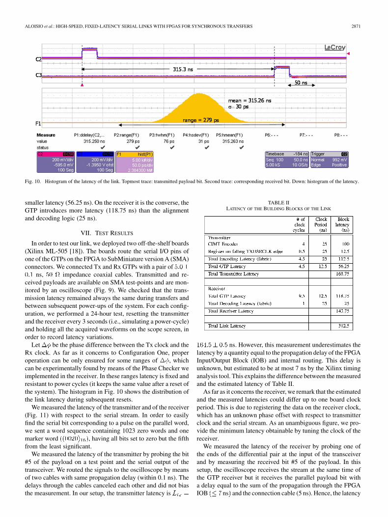
ns, impedance coaxial cables. Transmitted and re-ceived payloads are available on SMA test-points and are mon-itored by an oscilloscope (Fig. 9). We checked that the trans-mission latency remained always the same during transfers andbetween subsequent power-ups of the system. For each config-uration, we performed a 24-hour test, resetting the transmitterand the receiver every 3 seconds (i.e., simulating a power-cycle)and holding all the acquired waveforms on the scope screen, inorder to record latency variations.
Let be the phase difference between the Tx clock and theRx clock. As far as it concerns to Configuration One, properoperation can be only ensured for some ranges of , whichcan be experimentally found by means of the Phase Checker weimplemented in the receiver. In these ranges latency is fixed andresistant to power cycles (it keeps the same value after a reset ofthe system). The histogram in Fig. 10 shows the distribution ofthe link latency during subsequent resets.
We measured the latency of the transmitter and of the receiver(Fig. 11) with respect to the serial stream. In order to easilyfind the serial bit corresponding to a pulse on the parallel word,we sent a word sequence containing 1023 zero words and onemarker word , having all bits set to zero but the fifthfrom the least significant.
We measured the latency of the transmitter by probing the bit#5 of the payload on a test point and the serial output of thetransceiver. We routed the signals to the oscilloscope by meansof two cables with same propagation delay (within 0.1 ns). Thedelays through the cables canceled each other and did not biasthe measurement. In our setup, the transmitter latency is
TABLE IILATENCY OF THE BUILDING BLOCKS OF THE LINK
ns. However, this measurement underestimates thelatency by a quantity equal to the propagation delay of the FPGAInput/Output Block (IOB) and internal routing. This delay isunknown, but estimated to be at most 7 ns by the Xilinx timinganalysis tool. This explains the difference between the measuredand the estimated latency of Table II.
As far as it concerns the receiver, we remark that the estimatedand the measured latencies could differ up to one board clockperiod. This is due to registering the data on the receiver clock,which has an unknown phase offset with respect to transmitterclock and the serial stream. As an unambiguous figure, we pro-vide the minimum latency obtainable by tuning the clock of thereceiver.
We measured the latency of the receiver by probing one ofthe ends of the differential pair at the input of the transceiverand by measuring the received bit #5 of the payload. In thissetup, the oscilloscope receives the stream at the same time ofthe GTP receiver but it receives the parallel payload bit witha delay equal to the sum of the propagation through the FPGAIOB ns and the connection cable (5 ns). Hence, the latency

2872 IEEE TRANSACTIONS ON NUCLEAR SCIENCE, VOL. 56, NO. 5, OCTOBER 2009
Fig. 11. Oscilloscope screen-shots showing the latencies of the transmitter and of the receiver. (a) Upper trace: transmitted payload bit. Lower Trace: CIMTencoded serial stream. (b) Upper trace: CIMT encoded serial stream. Lower Trace: received payload bit.
is overestimated. The measured latency is ns,we subtracted the cable delay but not the IOB delay which weonly have an upper limit for.
As far as it concerns Configuration Two, the link transfersdata with a deterministic latency, which as before keeps thesame value after a power cycle. The latency of the transmitteris the same as in Configuration One. The latency of the receiverwas measured to be ns (without the cabledelay), thus the latency of the receiver increased by ns, dueto activation of the FIFO. The increment is not exactly 37.5 nsbecause of internal routing changes between the two implemen-tations. In this configuration, there are no limitations on buta very small forbidden interval ps , which leads to achange of latency of one board clock cycle between subsequentpower-ups of the link. We measured this interval by shifting theboard clocks with a step of 5 ps and checking whether or notfor 20 subsequent resets the link latency remained the same. Asdiscussed in Section II, this problem affects every synchronoussystem with an arbitrary skew on the clock distribution and itis not dependent on our design. For instance, the same effectoccurs with the original G-Link chip-set and with the Configu-ration One.
We also checked that our G-Link emulator is able to cor-rectly transmit (receive) data toward (from) an Agilent G-Linkreceiver (transmitter) chip. In order to perform this test, we de-ployed a ML-505 board and a custom board hosting a G-Linktransmitter and a receiver described in [19]. The test showed
that the emulator correctly exchanges data with a G-Link chipin both the CIMT encoding modes supported by the HDMP-1032/1034A chip-set.
VIII. CONCLUSIONS
High-speed SerDes embedded in FPGAs are typically de-signed for variable-latency transfers. However, by suitablyclocking and configuring two GTP transceivers embedded inXilinx FPGAs, we have been able to develop a fixed-latencylink for synchronous transfers. Our links requires a commonreference clock to be distributed both at the transmitter andat the receiver, like the global clock distributed by the TTCsystem in LHC experiments. The latency of the link is constantduring the transfer and even after a reset or a power-cycle of thesystem. We developed a clocking scheme and two configura-tions: one with minimum latency, which set some constraints onthe skew between the transmitter and receiver board clocks anda second one with a higher latency but without any constrainton the skew. Our configurations support an encoding/decodingexternal to the transceiver, thus they can be used with any serialprotocol. The only requirement is that the external encoding,coding and alignment is performed with a fixed latency. Weprovided guidelines to use our results also with Lattice andAltera embedded SerDes. However, the fixed-latency operationon those devices should be experimentally tested.
As an example application to discuss our architecture, wedesigned a serial link to be deployed in the ATLAS L1 barrel

ALOISIO et al.: HIGH-SPEED, FIXED-LATENCY SERIAL LINKS WITH FPGAS FOR SYNCHRONOUS TRANSFERS 2873
muon trigger receiver boards compatible with the AgilentG-Link chip-set. The link we implemented is also of interestfor the trigger system of the K Long Observation Experiment(KLOE) [20]. We successfully tested G-Link/GTPs hybridconfigurations. We deployed DLLs to provide the referenceclock on to the transceivers, but we have been allowed to do sothanks to the relatively low speed of the link (800 Mbps). Forhigher-speed links, the use of DLLs or PLLs should be avoidedsince their jitter performance may be insufficient to ensure areliable operation of the transceiver. We remark that GTPs canachieve multi-Gigabit data-rates 3.75 Gb/s and thereforeare appealing for deployment in super LHC experiments,where the requested bandwidth will increase with respect to thepresent.
ACKNOWLEDGMENT
The authors would like to thank G. Guasti and F. Contu ofXilinx Italy for their support and help in configuring the GTPtransceiver.
REFERENCES
[1] Ph. Busson, L. Dobrzynski, A. Karar, T. Romanteau, P. Moreira, J.L. Brelet, J. R. Macé, M. Défossez, M. Crowley, and C. Gannon,“Embedding deserialisation of LHC experimental data inside fieldprogrammable gate arrays,” in Proc. 8th Workshop on Electronics forLHC Experiments, 2002, Contribution ID A51.
[2] “Virtex-II Pro and Virtex-II Pro X Platform FPGAs: Complete DataSheet, Module 2,” Xilinx, 2007, pp. 10–17 [Online]. Available: http://www.xilinx.com/support/documentation/data_sheets/ds083.pdf
[3] P. Moreira, T. Toifl, A. Kluge, G. Cervelli, F. Faccio, A. Marchioro,and J. Christiansen, “G-link and gigabit ethernet compliant serializerfor LHC data transmission,” in Nucl. Sci. Symp. Conf. Rec., Oct. 15–20,2000, vol. 2, pp. 9/6–9/9.
[4] C.-S. Yen, R. C. Walker, P. T. Petruno, C. Stout, B. W. H. Lai, and W.J. McFarland, “G-link: A chipset for gigabit-rate data communication,”Hewlett Packard J., vol. 43, no. 5, pp. 103–115, Oct. 1992.
[5] G. Aglieri Rinella, A. Klugea, and M. Krivdaab, “The level 0 pixeltrigger system for the ALICE experiment,” J. Instrumen., vol. 1, no. 1,p. P01007, 2007.
[6] A. Hidvégi, D. Eriksson, and C. Bohm, “A small portable test systemfor the TileCal Digitizer System,” in Proc. Topical Workshop onElectronics for Particle Physics, Naxos, Greece, Sep. 19, 2008, pp.513–515.
[7] G. Iles et al., “Performance and lessons of the CMS global calorimetertrigger,” in Proc. Topical Workshop on Electronics for Particle Physics,Naxos, Greece, Sep. 15–19, 2008, pp. 129–132.
[8] E. Aslanides et al., “The level-0 Muon Trigger for the LHCb experi-ment,” Nuclear Instruments and Methods in Physics Research, SectionA, vol. 579, no. 3, pp. 989–1004, 2007.
[9] P. Moreira and A. M. Kloukinas, “The GBT : A proposed architecurefor multi-Gb/s data transmission in high energy physics,” in Proc. Top-ical Workshop on Electronics for Particle Physics, Prague, Czech Re-public, Sep. 3–7, 2007, pp. 332–336.
[10] “ATLAS Detector and Physics Performance, Technical Design Re-port Volume I,” ATLAS Collaboration, 1999 [Online]. Available:http://atlas.web.cern.ch/Atlas/GROUPS/PHYSICS/TDR/physics_tdr/printout/Volume_I.pdf
[11] B. G. Taylor, for the RD12 project collaboration, “TTC distribution forLHC detectors,” IEEE Trans. Nucl. Sci. vol. 45, no. 3, pp. 821–828,Jun. 1998..
[12] R. C. Walker, C. L. Stout, J. Wu, B. Lai, C. Yen, T. Hornak, and P.T. Petruno, “A two-chip 1.5-GBd serial link interface,” IEEE J. Solid-State Circuits, vol. 21, no. 12, pp. 1805–1811, Dec. 1992.
[13] “Agilent HDMP 1032-1034 Transmitter-Receiver Chipset Datasheet,”Agilent, 2001 [Online]. Available: http://www.physics.ohio-state.edu/~cms/cfeb/datasheets/hdmp1032.pdf
[14] S. H. Unger and C. J. Tan, “Clocking schemes for high-speed digitalsystems,” IEEE Trans. Comput., vol. C-35, no. 10, pp. 880–895, Oct.1986.
[15] “Virtex-5 FPGA RocketIO GTP Transceiver User Guide, UG196 (v1.7),” Xilinx, 2008 [Online]. Available: http://www.xilinx.com/support/documentation/user_guides/ug196.pdf
[16] “Stratix IV Device Handbook,” Altera, 2008 [Online]. Available: http://www.altera.com/literature/hb/stratix-iv/stratix4_handbook.pdf
[17] “LatticeSC/M Family Data Sheet,” Lattice Semiconductor Corp.,2008 [Online]. Available: http://www.latticesemi.com/docu-ments/DS1005.pdf
[18] “ML505/ML506/ML507 Evaluation Platform User Guide, UG347(v3.0.1),” Xilinx, 2008 [Online]. Available: http://www.xilinx.com/support/documentation/boards_and_kits/ug347.pdf
[19] A. Aloisio, F. Cevenini, and V. Izzo, “Do’s and don’ts with theAgilent’s G-link chipset,” IEEE Trans. Nucl. Sci., vol. 53, no. 3, pp.795–800, Jun. 2006.
[20] M. Adinolfi et al., “The trigger system of the KLOE experiment,” Nucl.Instr. Meth., vol. A492, pp. 134–146, 2002.