2/8/06D&T Seminar1 Multi-Core Parallelism for Low- Power Design Vishwani D. Agrawal James J. Danaher...
29
2/8/06 D&T Seminar 1 Multi-Core Parallelism for Low-Power Design Vishwani D. Agrawal James J. Danaher Professor Department of Electrical and Computer Engineering Auburn University http://www.eng.auburn.edu/~vagrawal [email protected]
-
date post
21-Dec-2015 -
Category
Documents
-
view
214 -
download
0
Transcript of 2/8/06D&T Seminar1 Multi-Core Parallelism for Low- Power Design Vishwani D. Agrawal James J. Danaher...
2/8/06 D&T Seminar 1
Multi-Core Parallelism for Low-Power Design
Vishwani D. AgrawalJames J. Danaher Professor
Department of Electrical and Computer EngineeringAuburn University
http://www.eng.auburn.edu/[email protected]
2/8/06 D&T Seminar 2
Power Consumption of VLSI Chips
Why is it a concern?

2/8/06 D&T Seminar 3
SIA Roadmap for Processors (1999)Year 1999 2002 2005 2008 2011 2014
Feature size (nm) 180 130 100 70 50 35
Logic transistors/cm2 6.2M 18M 39M 84M 180M 390M
Clock (GHz) 1.25 2.1 3.5 6.0 10.0 16.9
Chip size (mm2) 340 430 520 620 750 900
Power supply (V) 1.8 1.5 1.2 0.9 0.6 0.5
High-perf. Power (W) 90 130 160 170 175 183
Source: http://www.semichips.org

2/8/06 D&T Seminar 4
ISSCC, Feb. 2001, Keynote“Ten years from now, microprocessors will run at 10GHz to 30GHz and be capable of processing 1 trillion operations per second -- about the same number of calculations that the world's fastest supercomputer can perform now.
“Unfortunately, if nothing changes these chips will produce as much heat, for their proportional size, as a nuclear reactor. . . .”
Patrick P. Gelsinger Senior Vice PresidentGeneral ManagerDigital Enterprise Group INTEL CORP.
2/8/06 D&T Seminar 5
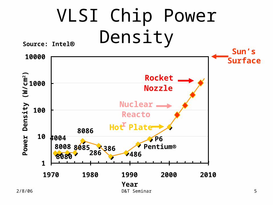
VLSI Chip Power Density
40048008
80808085
8086
286386
486Pentium®
P6
1
10
100
1000
10000
1970 1980 1990 2000 2010
Year
Po
wer
Den
sity
(W
/cm
2 )
Hot Plate
NuclearReactor
RocketNozzle
Sun’sSurface
Source: Intel
2/8/06 D&T Seminar 6
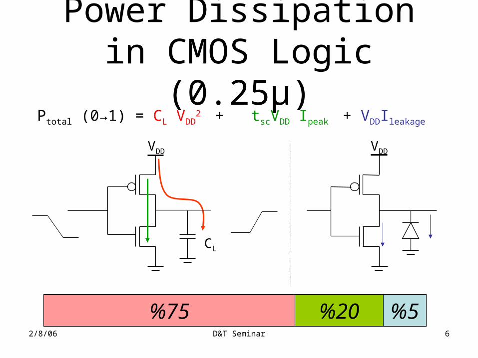
Power Dissipation in CMOS Logic (0.25µ)
%75 %5%20
Ptotal (0→1) = CL VDD2
+ tscVDD Ipeak + VDDIleakage
CL
VDD VDD

2/8/06 D&T Seminar 7
Low-Power Datapath Architecture• Lower supply voltage
– This slows down circuit speed– Use parallel computing to gain the speed back
• Works well when threshold voltage is also lowered.
• About 60% reduction in power obtainable.• Reference: A. P. Chandrakasan and R. W.
Brodersen, Low Power Digital CMOS Design, Boston: Kluwer Academic Publishers (Now Springer), 1995.
2/8/06 D&T Seminar 8
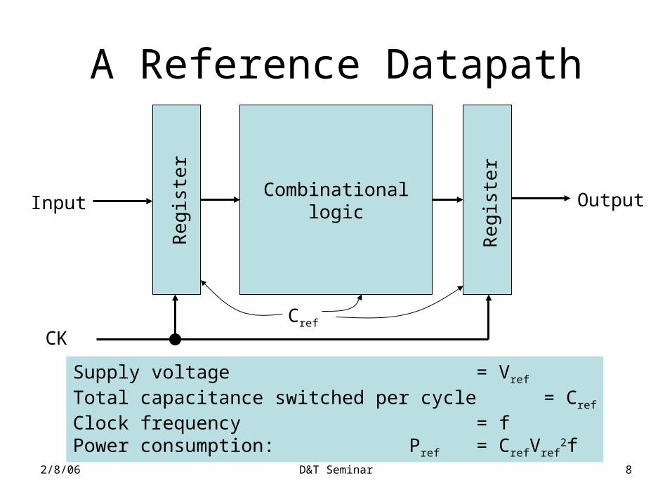
A Reference Datapath
Combinationallogic
OutputInputR
eg
iste
r
Re
gis
ter
CK
Supply voltage = Vref
Total capacitance switched per cycle = Cref
Clock frequency = fPower consumption: Pref = CrefVref
2f
Cref

2/8/06 D&T Seminar 9
A Parallel ArchitectureComb.Logic
Copy 1
Comb.Logic
Copy 2
Comb.Logic
Copy N
Re
gis
ter
Re
gis
ter
Re
gis
ter
Re
gis
ter
N to
1 m
ulti
ple
xer
MultiphaseClock gen. and mux
control
InputOutput
CK
f
f/N
f/N
f/N
A copy processes every Nth input, operates at reduced voltage
Supply voltage:VN ≤ V1 = Vref
N = Deg. of parallelism

2/8/06 D&T Seminar 10
Control Signals, N = 4
CK
Phase 1
Phase 2
Phase 3
Phase 4

2/8/06 D&T Seminar 11
PowerPN = Pproc + Poverhead
Pproc = N(Cinreg+ Ccomb)VN2f/N + CoutregVN
2f
= (Cinreg+ Ccomb+Coutreg)VN2f
= CrefVN2f
Poverhead = CoverheadVN2f ≈ δCref(N – 1)VN
2f
PN = [1 + δ(N – 1)]CrefVN2f
PN VN2
── = [1 + δ(N – 1)] ───P1 Vref
2

2/8/06 D&T Seminar 12
Voltage vs. Speed CLVref CLVref
Delay of a gate, T ≈ ──── = ────────── I k(W/L)(Vref – Vt)2
where I is saturation currentk is a technology parameterW/L is width to length ratio of transistorVt is threshold voltage
Supply voltage
No
rma
lize
d g
ate
de
lay,
T
4.0
3.0
2.0
1.0
0.0 Vt Vref =5VV2=2.9V
N=1
N=2
V3
N=31.2μ CMOS Voltage reduction
slows down as we get closer to Vt
2/8/06 D&T Seminar 13
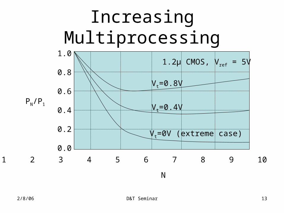
Increasing Multiprocessing
PN/P1
1 2 3 4 5 6 7 8 9 10 11 12
1.0
0.8
0.6
0.4
0.2
0.0
Vt=0V (extreme case)
Vt=0.4V
Vt=0.8V
N
1.2μ CMOS, Vref = 5V
2/8/06 D&T Seminar 14
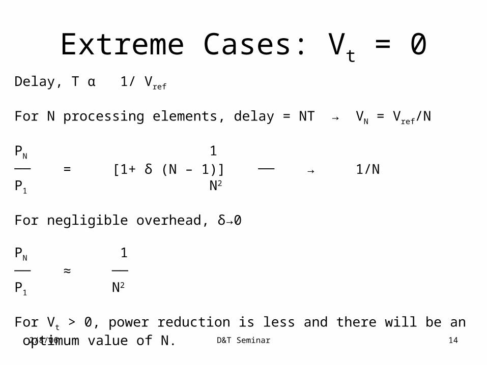
Extreme Cases: Vt = 0Delay, T α 1/ Vref
For N processing elements, delay = NT → VN = Vref/N
PN 1── = [1+ δ (N – 1)] ── → 1/NP1 N2
For negligible overhead, δ→0
PN 1── ≈ ──P1 N2
For Vt > 0, power reduction is less and there will be an optimum value of N.

2/8/06 D&T Seminar 15
Example: Multiplier Core
• Specification:• 200MHz Clock• 15W dissipation @ 5V• Low voltage operation, VDD ≥ 1.5 volts
(VDD – 0.5)2
Relative clock rate = ─────── 20.25
• Problem:• Integrate multiplier core on a SOC• Power budget for multiplier ~ 5W

2/8/06 D&T Seminar 16
A Multicore Design
MultiplierCore 1
MultiplierCore 5
Reg
RegR
egR
eg
5 to
1 m
ux
MultiphaseClock gen.
and muxcontrol
Input
Output
200MHzCK
200MHz
40MHz
40MHz
40MHz
MultiplierCore 2
Core clock frequency = 200/N, N should divide 200.

2/8/06 D&T Seminar 17
How Many Cores?
• For N cores:• clock frequency = 200/N MHz
• Supply voltage, VDDN= 0.5 + (20.25/N)1/2 Volts
• Assuming 10% overhead per core, VDDN
Power dissipation =15 [1 + 0.1(N – 1)] (───)2
watts 5

2/8/06 D&T Seminar 18
Design TradeoffsNumber of cores
NClock (MHz)
Core supply VDDN (Volts)
Total Power
(Watts)
1 200 5.00 15.0
2 100 3.68 8.94
4 50 2.75 5.90
5 40 2.51 5.29
8 25 2.10 4.50

2/8/06 D&T Seminar 19
Power Reduction in Processors
• Just about everything is used.• Hardware methods:
• Voltage reduction for dynamic power• Dual-threshold devices for leakage reduction• Clock gating, frequency reduction• Sleep mode
• Architecture:• Instruction set• hardware organization
• Software methods

2/8/06 D&T Seminar 20
Parallel Architecture
Processor
f
Processor
f/2
Processor
f/2
f
Input Output
Input
Output
Capacitance = CVoltage = VFrequency = fPower = CV2f
Capacitance = 2.2CVoltage = 0.6VFrequency = 0.5fPower = 0.396CV2f

2/8/06 D&T Seminar 21
Pipeline Architecture
Processor
f
Input Output
Re
gis
ter
½Proc.
f
Input Output
Re
gis
ter
½Proc.
Re
gis
ter
Capacitance = CVoltage = VFrequency = fPower = CV2f
Capacitance = 1.2CVoltage = 0.6VFrequency = fPower = 0.432CV2f

2/8/06 D&T Seminar 22
Approximate Trend n-parallel proc. n-stage pipeline proc.
Capacitance nC C
Voltage V/n V/n
Frequency f/n f
Power CV2f/n2 CV2f/n2
Chip area n times 10-20% increase
G. K. Yeap, Practical Low Power Digital VLSI Design, Boston: KluwerAcademic Publishers, 1998.
2/8/06 D&T Seminar 23
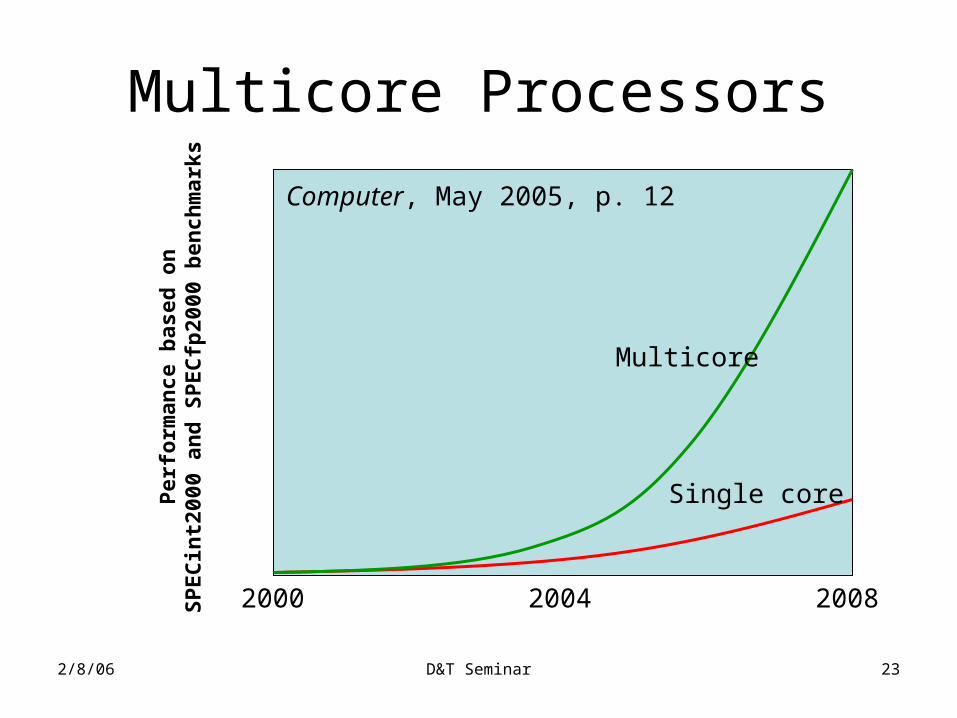
Multicore Processors
2000 2004 2008
Per
form
ance
bas
ed o
nS
PE
Cin
t200
0 an
d S
PE
Cfp
2000
ben
chm
arks
Multicore
Single core
Computer, May 2005, p. 12

2/8/06 D&T Seminar 24
Multicore Processors
• D. Geer, “Chip Makers Turn to Multicore Processors,” Computer, vol. 38, no. 5, pp. 11-13, May 2005.
• A. Jerraya, H. Tenhunen and W. Wolf, “Multiprocessor Systems-on-Chips,” Computer, vol. 5, no. 7, pp. 36-40, July 2005; this special issue contains three more articles on multicore processors.
• S. K. Moore, “Winner Multimedia Monster – Cell’s Nine Processors Make It a Supercomputer on a Chip,” IEEE Spectrum, vol. 43. no. 1, pp. 20-23, January 2006.
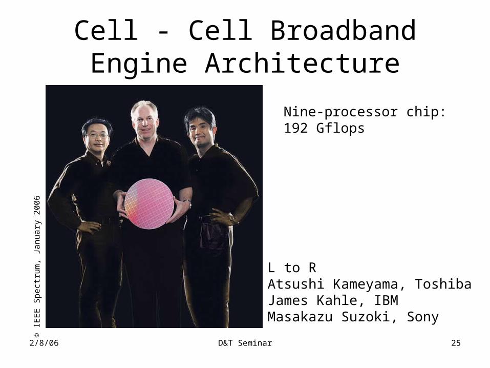
2/8/06 D&T Seminar 25
Cell - Cell Broadband Engine Architecture
L to RAtsushi Kameyama, ToshibaJames Kahle, IBMMasakazu Suzoki, Sony
© I
EE
E S
pe
ctru
m,
Jan
ua
ry 2
00
6
Nine-processor chip:192 Gflops

2/8/06 D&T Seminar 26
Cell’s Nine-Processor Chip
© IEEE Spectrum, January 2006 Eight IdenticalProcessors f = 5.6GHz (max)44.8 Gflops

2/8/06 D&T Seminar 27
?

2/8/06 D&T Seminar 28
Amdahl’s Law
S P = 1 – S
0 1 time 1
Speedup = ─────────S + (1 – S)/ N
Where N = number of parallel processors
Example: S = 0.6, N = 10, Speedup = 1.56S = 0.6, N = ∞, Speedup = 1.67
Gene Amdahl, “Validity of the Single Processor Approach to Achieving Large-Scale Computing Capabilities,” AFIPS Conference Proceedings, (30), pp. 483-485, 1967.

2/8/06 D&T Seminar 29
Question
• Can we find a multi-processing law– for power reduction, or– for performance per watt