2566 IEEE TRANSACTIONS ON MICROWAVE THEORY AND …klwu/pdf/mtt201307.pdf · 2568 IEEE TRANSACTIONS...
8
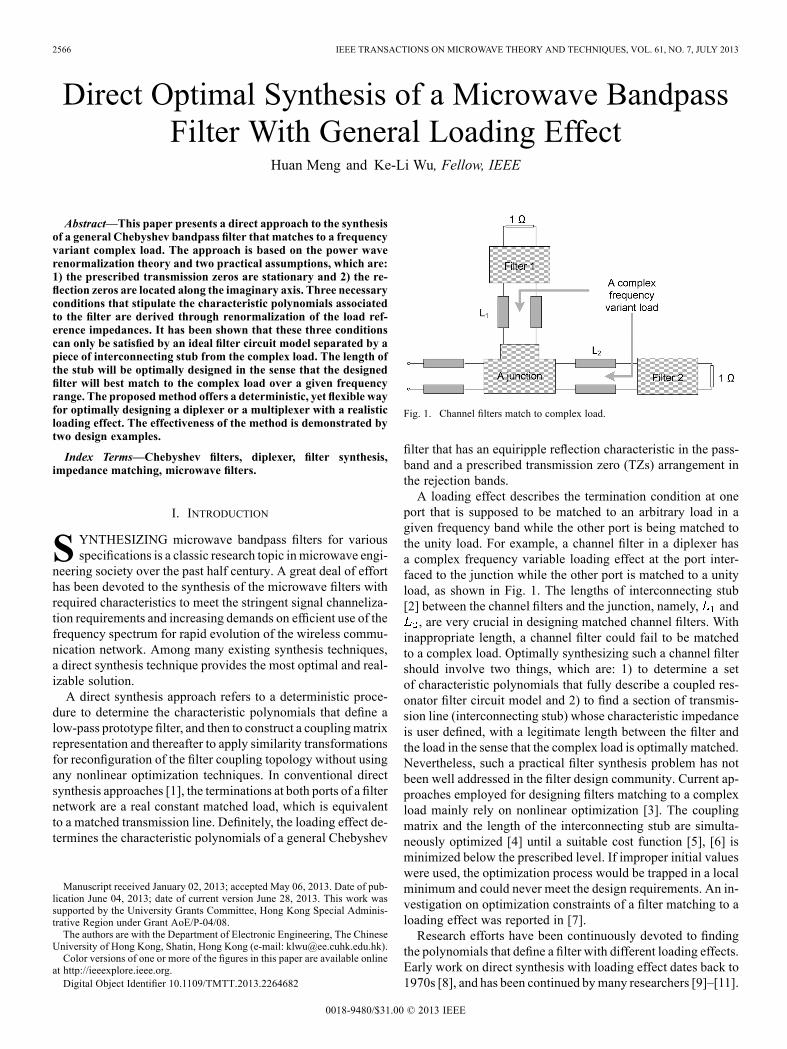
2566 IEEE TRANSACTIONS ON MICROWAVE THEORY AND TECHNIQUES, VOL. 61, NO. 7, JULY 2013 Direct Optimal Synthesis of a Microwave Bandpass Filter With General Loading Effect Huan Meng and Ke-Li Wu, Fellow, IEEE Abstract—This paper presents a direct approach to the synthesis of a general Chebyshev bandpass filter that matches to a frequency variant complex load. The approach is based on the power wave renormalization theory and two practical assumptions, which are: 1) the prescribed transmission zeros are stationary and 2) the re- flection zeros are located along the imaginary axis. Three necessary conditions that stipulate the characteristic polynomials associated to the filter are derived through renormalization of the load ref- erence impedances. It has been shown that these three conditions can only be satisfied by an ideal filter circuit model separated by a piece of interconnecting stub from the complex load. The length of the stub will be optimally designed in the sense that the designed filter will best match to the complex load over a given frequency range. The proposed method offers a deterministic, yet flexible way for optimally designing a diplexer or a multiplexer with a realistic loading effect. The effectiveness of the method is demonstrated by two design examples. Index Terms—Chebyshev filters, diplexer, filter synthesis, impedance matching, microwave filters. I. INTRODUCTION S YNTHESIZING microwave bandpass filters for various specifications is a classic research topic in microwave engi- neering society over the past half century. A great deal of effort has been devoted to the synthesis of the microwave filters with required characteristics to meet the stringent signal channeliza- tion requirements and increasing demands on efficient use of the frequency spectrum for rapid evolution of the wireless commu- nication network. Among many existing synthesis techniques, a direct synthesis technique provides the most optimal and real- izable solution. A direct synthesis approach refers to a deterministic proce- dure to determine the characteristic polynomials that define a low-pass prototype filter, and then to construct a coupling matrix representation and thereafter to apply similarity transformations for reconfiguration of the filter coupling topology without using any nonlinear optimization techniques. In conventional direct synthesis approaches [1], the terminations at both ports of a filter network are a real constant matched load, which is equivalent to a matched transmission line. Definitely, the loading effect de- termines the characteristic polynomials of a general Chebyshev Manuscript received January 02, 2013; accepted May 06, 2013. Date of pub- lication June 04, 2013; date of current version June 28, 2013. This work was supported by the University Grants Committee, Hong Kong Special Adminis- trative Region under Grant AoE/P-04/08. The authors are with the Department of Electronic Engineering, The Chinese University of Hong Kong, Shatin, Hong Kong (e-mail: [email protected]). Color versions of one or more of the figures in this paper are available online at http://ieeexplore.ieee.org. Digital Object Identifier 10.1109/TMTT.2013.2264682 Fig. 1. Channel filters match to complex load. filter that has an equiripple reflection characteristic in the pass- band and a prescribed transmission zero (TZs) arrangement in the rejection bands. A loading effect describes the termination condition at one port that is supposed to be matched to an arbitrary load in a given frequency band while the other port is being matched to the unity load. For example, a channel filter in a diplexer has a complex frequency variable loading effect at the port inter- faced to the junction while the other port is matched to a unity load, as shown in Fig. 1. The lengths of interconnecting stub [2] between the channel filters and the junction, namely, and , are very crucial in designing matched channel filters. With inappropriate length, a channel filter could fail to be matched to a complex load. Optimally synthesizing such a channel filter should involve two things, which are: 1) to determine a set of characteristic polynomials that fully describe a coupled res- onator filter circuit model and 2) to find a section of transmis- sion line (interconnecting stub) whose characteristic impedance is user defined, with a legitimate length between the filter and the load in the sense that the complex load is optimally matched. Nevertheless, such a practical filter synthesis problem has not been well addressed in the filter design community. Current ap- proaches employed for designing filters matching to a complex load mainly rely on nonlinear optimization [3]. The coupling matrix and the length of the interconnecting stub are simulta- neously optimized [4] until a suitable cost function [5], [6] is minimized below the prescribed level. If improper initial values were used, the optimization process would be trapped in a local minimum and could never meet the design requirements. An in- vestigation on optimization constraints of a filter matching to a loading effect was reported in [7]. Research efforts have been continuously devoted to finding the polynomials that define a filter with different loading effects. Early work on direct synthesis with loading effect dates back to 1970s [8], and has been continued by many researchers [9]–[11]. 0018-9480/$31.00 © 2013 IEEE
Transcript of 2566 IEEE TRANSACTIONS ON MICROWAVE THEORY AND …klwu/pdf/mtt201307.pdf · 2568 IEEE TRANSACTIONS...
2566 IEEE TRANSACTIONS ON MICROWAVE THEORY AND TECHNIQUES, VOL. 61, NO. 7, JULY 2013
Direct Optimal Synthesis of a Microwave BandpassFilter With General Loading Effect
Huan Meng and Ke-Li Wu, Fellow, IEEE
Abstract—This paper presents a direct approach to the synthesisof a general Chebyshev bandpass filter that matches to a frequencyvariant complex load. The approach is based on the power waverenormalization theory and two practical assumptions, which are:1) the prescribed transmission zeros are stationary and 2) the re-flection zeros are located along the imaginary axis. Three necessaryconditions that stipulate the characteristic polynomials associatedto the filter are derived through renormalization of the load ref-erence impedances. It has been shown that these three conditionscan only be satisfied by an ideal filter circuit model separated by apiece of interconnecting stub from the complex load. The length ofthe stub will be optimally designed in the sense that the designedfilter will best match to the complex load over a given frequencyrange. The proposedmethod offers a deterministic, yet flexible wayfor optimally designing a diplexer or a multiplexer with a realisticloading effect. The effectiveness of the method is demonstrated bytwo design examples.
Index Terms—Chebyshev filters, diplexer, filter synthesis,impedance matching, microwave filters.
I. INTRODUCTION
S YNTHESIZING microwave bandpass filters for variousspecifications is a classic research topic inmicrowave engi-
neering society over the past half century. A great deal of efforthas been devoted to the synthesis of the microwave filters withrequired characteristics to meet the stringent signal channeliza-tion requirements and increasing demands on efficient use of thefrequency spectrum for rapid evolution of the wireless commu-nication network. Among many existing synthesis techniques,a direct synthesis technique provides the most optimal and real-izable solution.A direct synthesis approach refers to a deterministic proce-
dure to determine the characteristic polynomials that define alow-pass prototype filter, and then to construct a couplingmatrixrepresentation and thereafter to apply similarity transformationsfor reconfiguration of the filter coupling topology without usingany nonlinear optimization techniques. In conventional directsynthesis approaches [1], the terminations at both ports of a filternetwork are a real constant matched load, which is equivalentto a matched transmission line. Definitely, the loading effect de-termines the characteristic polynomials of a general Chebyshev
Manuscript received January 02, 2013; accepted May 06, 2013. Date of pub-lication June 04, 2013; date of current version June 28, 2013. This work wassupported by the University Grants Committee, Hong Kong Special Adminis-trative Region under Grant AoE/P-04/08.The authors are with the Department of Electronic Engineering, The Chinese
University of Hong Kong, Shatin, Hong Kong (e-mail: [email protected]).Color versions of one or more of the figures in this paper are available online
at http://ieeexplore.ieee.org.Digital Object Identifier 10.1109/TMTT.2013.2264682
Fig. 1. Channel filters match to complex load.
filter that has an equiripple reflection characteristic in the pass-band and a prescribed transmission zero (TZs) arrangement inthe rejection bands.A loading effect describes the termination condition at one
port that is supposed to be matched to an arbitrary load in agiven frequency band while the other port is being matched tothe unity load. For example, a channel filter in a diplexer hasa complex frequency variable loading effect at the port inter-faced to the junction while the other port is matched to a unityload, as shown in Fig. 1. The lengths of interconnecting stub[2] between the channel filters and the junction, namely, and, are very crucial in designing matched channel filters. With
inappropriate length, a channel filter could fail to be matchedto a complex load. Optimally synthesizing such a channel filtershould involve two things, which are: 1) to determine a setof characteristic polynomials that fully describe a coupled res-onator filter circuit model and 2) to find a section of transmis-sion line (interconnecting stub) whose characteristic impedanceis user defined, with a legitimate length between the filter andthe load in the sense that the complex load is optimally matched.Nevertheless, such a practical filter synthesis problem has notbeen well addressed in the filter design community. Current ap-proaches employed for designing filters matching to a complexload mainly rely on nonlinear optimization [3]. The couplingmatrix and the length of the interconnecting stub are simulta-neously optimized [4] until a suitable cost function [5], [6] isminimized below the prescribed level. If improper initial valueswere used, the optimization process would be trapped in a localminimum and could never meet the design requirements. An in-vestigation on optimization constraints of a filter matching to aloading effect was reported in [7].Research efforts have been continuously devoted to finding
the polynomials that define a filter with different loading effects.Early work on direct synthesis with loading effect dates back to1970s [8], and has been continued bymany researchers [9]–[11].
0018-9480/$31.00 © 2013 IEEE

MENG AND WU: DIRECT OPTIMAL SYNTHESIS OF MICROWAVE BANDPASS FILTER 2567
Recently, a direct diplexer synthesis approach was proposed in[12], which is essentially a method of determining the polyno-mials with the loading effect of a lumped-element Y-junctionin shunt connection with the other channel filter. The approachdeals with the loading effect that can only be described by alumped-element circuit model. Three inconveniences of theseapproaches [8]–[12] are: 1) the complex load is restricted to alimited number of lumped element circuits; 2) high-order poly-nomials must be dealt with in uncertain accuracy; and 3) notransmission-line effect can be incorporated. An approach wasproposed in [13] for handling an arbitrary frequency invariantcomplex load for narrowband filter design applications. An at-tempt was made to extend the approach to handle an arbitraryfrequency variant complex load by an admittance approach [14].Two intrinsic limitations to this admittance approach are: 1) itlacks of a mechanism to find a section of interconnecting stubbetween the load and the filter for optimal impedance matchingand 2) there is no rationale in setting up the objective charac-teristic polynomials, resulting in a network that can never berealized with lumped or distributed elements.In this paper, a direct optimal synthesis approach to the de-
sign of a general Chebyshev bandpass filter that is matched toa general complex loading effect is proposed. The proposedtheory is based on the power wave renormalization theory [15]and two practical assumptions, which are: 1) the prescribed TZsare stationary and 2) the reflection zeros are located along theimaginary axis of the complex frequency plane. These two as-sumptions were also used in [12] where a simple junction cir-cuit model for diplexer design was considered. The first assump-tion imposes the prescribed filter topology and ensures the rejec-tion-rate satisfy the design requirements; the latter assumptionfacilitates the synthesis: among various possible transfer func-tions, synthesis of a Chebyshev filter whose reflection zeros arepurely imaginary is an analytical process [1]. Unlike the methodpresented in [16] by the same authors, where the reflection zerosare determined solely by the prescribed TZs, objective polyno-mials depend on the complex load, and consequently the reflec-tion zeros are also load dependent in the proposed method. Thisimprovement is very important as the loading effect will be in-corporated in setting up a set of realistically objective polyno-mials with equiripple return-loss characteristic in the passband.In this paper, a general loading effect is defined by the compleximpedance over a sufficiently wide band of actual frequency. The impedance is then transferred to the low-pass domainby the frequency transformation ,where and are the bandwidth and center frequency ofthe filter, respectively. In the discussion below, variable refersto the complex frequency variable in the low-pass domain. Thecoupling elements (and matrix) are also defined in the low-passdomain. With the proposed approach, designing a multiplexeror a diplexer becomes a matter of synthesizing an individualchannel filter and optimally determining an interconnecting stubfor matching to a general complex load.By introducing a piece of interconnecting stub, designing a
matched filter to a generalized complex load with reflectionzeros located on imaginary axis can be greatly facilitated. A de-tailed synthesis procedure is described by a step-by-step proce-dure. The effectiveness of the method is demonstrated by twodesign examples.
Fig. 2. Same filter network referenced to different reference load and its cor-responding approximation.
II. THEORY
A. Stipulation Conditions
Considering a matched filter network whose one port is con-nected to a general frequency variant load and the other port isreferenced to the unity load, as shown in Fig. 2(a), to complywith the definition of a coupling matrix, the characteristic poly-nomials of the filter must be referenced to unity loads at bothports. Directly synthesizing the filter network becomes a matterof finding the characteristic polynomials of the filter that is ref-erenced to the unity load at the two ports and a section of inter-connecting stub between the filter and load. The basic conceptof the renormalization is illustrated in Fig. 2: the system func-tion in Fig. 2(a) is assumed to be known with port 1 and port2 connected to the unity load and a general complex load ,respectively.When the reference impedance at port 2 is changedto unity load, the system function of the same filter network,as defined by Fig. 2(b), can be obtained by power wave renor-malization [15] as
(1a)
(1b)
where , denotes the complex con-jugate, and is the complex impedance at port 2. Although(1) is valid at any frequency band, to comply with the conven-tion in filter synthesis, all the variables are transformed to thelow-pass domain in this study. Until now, two sets of character-istic polynomials have been defined: one describes the objectivefilter responses defined by with
(2a)

2568 IEEE TRANSACTIONS ON MICROWAVE THEORY AND TECHNIQUES, VOL. 61, NO. 7, JULY 2013
and the other specifies the measurable response of of thesame filter network, which is referenced to the unity load
(2b)
Although the characteristic polynomials are defined in thecomplex plane, in evaluating (1) and (2), will be stipulatedto as only is measurable frequency. Defining charac-teristic polynomials in the complex plane is to find wide sensedefined system functions that best satisfy various filter perfor-mance requirements along the axis. Substituting (2)into (1) and using the equation of the conservation of power,the polynomials defining can be obtained by
Transference (3a)
Matchability (3b)
Conservativeness (3c)
The equations in (3) are the conditions stipulating the objec-tive polynomials and and the polynomials
and that describe an approximation of thecorresponding measurable responses. Again, the validation do-main for when evaluating (3) is alone the axis. For a gen-eral loading effect in a broadband sense, it is impossible to finda set of solutions that satisfy (3) in the entire frequency band.However, one can find a set of optimally approximated and re-alizable solutions of and by conveniently choosingthe same order of and , respectively, to satisfy (3)over a given frequency band. The choice allows the order andthe coupling topology of the filter to be fixed.It will be approved later in this paper that a good approximate
solution to (3) can be achieved by a realizable filter networkand a section of interconnecting stub between the load and thefilter network. It will be shown that the filter network ismeasurable as it is referenced to the unity load at both ports, asshown in Fig. 2(c), andmost importantly it can be described by acoupled resonator bandpass filter circuit model. In the proposedapproach, an optimal length of the interconnecting stub will bedetermined in the sense that the conservativeness condition in(3) is optimally satisfied under the two proposed assumptions.
B. Direct Synthesis Approach
It is apparent from (3) that the characteristic polynomials ofthe filter network to be designed depend on the loading effect
as well as the objective polynomials , , and .Therefore, the objective polynomials must be achievable, loaddependent, and satisfy the required specifications. The proposedsynthesizing approach starts with finding a set of legitimateobjective polynomials. The detailed step-by-step procedure isgiven by the following steps.Step 1) Stipulating the measurable polynomial as
(4)
where refers to the th prescribed TZ anddenotes the number of TZs. In addition, andare two unknown parameters to be determined andcan be temporally set to 1 and 0, respectively. Inpractice, a proper selection of prescribed TZs wouldensure the required rejections and group delay for afilter of a given order. Note that the TZs need to besymmetric about the imaginary axis.
Step 2) Determining the objective polynomial by thetransference condition (3a) using linear least squaresfitting [17] over the passband of the designed filter.To avoid an ill-posed problem, the number of sam-ples should be at least larger than the filter orderplus one. In general, 50 or more points are sug-
gested. The order of can be increased to fullyreflect the effect of frequency variant load and tominimize the least square error. Denote the roots of
as , where is smaller than. It is apparent that, according to the transference
condition, not only shares the TZs of ,but also possibly incorporates extra zeros caused bythe complex load. It will be shown later that the syn-thesized filter network will possess the same TZs asthose of . This is called TZ stationary property.
Step 3) Synthesizing the objective polynomials andand the normalization constant that sat-
isfy a general Chebyshev characteristic with, obtained in Step 2, the pre-
scribed return-loss level RL in decibels and the filterorder . To this end, a well-established procedureis available in [1]. In this step, the normalizationconstant will be updated by .
Step 4) With a set of realistic objective polynomialsand known, can be ap-
proximately obtained using matchability condition(3b) by linear least square fitting with the sameorder as that of . It must be noted thatis not monic and its coefficient of the th-orderterm is a complex number in general and can beexpressed as .
Step 5) Having had known (in Step 1), and(in Step 3 and Step 4, respectively), the roots [theth zero of the polynomial ] and of theobjective polynomial can be determined usingthe conservation of power equation
(5)
where is the coefficient of the th-order term ofand refers to the magnitude. It is apparent
that , whereas the phase of , ,can be optimally selected to minimize the error insatisfying conservativeness condition (3c) definedby
error (6)

MENG AND WU: DIRECT OPTIMAL SYNTHESIS OF MICROWAVE BANDPASS FILTER 2569
where denotes the numerical value of theright-hand side of (3c) at the th sampling fre-quency in the low-pass domain. Note that althoughthe system and is measurable,it does not necessarily describe a coupled resonatorfilter circuit model because, in general, .
Step 6) Specifying a set of new polynomialsand from the system andby
(7a)
(7b)
(7c)
where is the coefficient of the th-order term of. The approximation sign in (7b) means that
(3c) can be optimally satisfied by adjusting phase. By normalizing to the highest coefficients
and , respectively, the resultantand can fully describe a coupled resonatorfilter network because they satisfy the followingconditions:1) power conservation;2) roots of reside in the left half of complexplane;
3) roots of are symmetric about the imagi-nary axis;
4) polynomials and aremonic.
According to (2b), the scattering parameters of a measurablenetwork that is matched to a general complex load in a givenfrequency band can thus be expressed as
(8a)
(8b)
where the relations andare implied. Equation (8) reveals that the network,
which best matches to the general complex loading in a givenfrequency band, consists of an ideal coupled resonator filter de-fined by polynomials and and a sectionof optimally designed interconnecting stub between the idealfilter and load. The electrical length is optimal in the sense thatit minimizes the error in satisfying conservativeness condition(3c). This mixed network is depicted in Fig. 2(c). It is a commonpractice that the characteristic impedance of the interconnectingstub is user defined and is used in measuring the value of thecomplex load. Although the phase constant is frequency in-dependent, it represents a very good approximation of a pieceof transmission by the electric length at the center frequency ofa passband filter and is irrelevant to the dispersive relation ofa particular type of transmission line. For most of the channelfilter applications, where the fractional bandwidth is only abouta few percent, this approximation works very well.
It is seen that is found at the last stage and theoreticallyshould be updated accordingly. However, takes no ef-
fect in the proposed procedure since it only contributes a con-stant phase to and consequently , whereas the rootswill not be altered. The phase provision is introduced in (4)
in order to ensure be realizable as .Under the assumption that the reflection zeros are located
along the imaginary axis, the combined filter and an idealtransmission line network does not always ensure a perfectimpedance matching. Such mismatching is reflected by theminimal error in searching for an optimal by applyingconservativeness condition 3(c). It is found that the matchingcondition can be improved when the complex load presentsmore stationary variation versus frequency.
III. PRACTICAL DESIGN EXAMPLES
A. Diplexer Design Using an -Plane T-Junction
To illustrate the effectiveness of the proposed method, thedetailed design procedure for an -plane waveguide diplexeris given here. The diplexer has two fourth-order all-pole fil-ters connected to a WR62 -plane T-junction. An iterative ap-proach is applied to each channel filter design until the diplexererror, which is defined as
diplexer error minimum error of -th channel
(9)
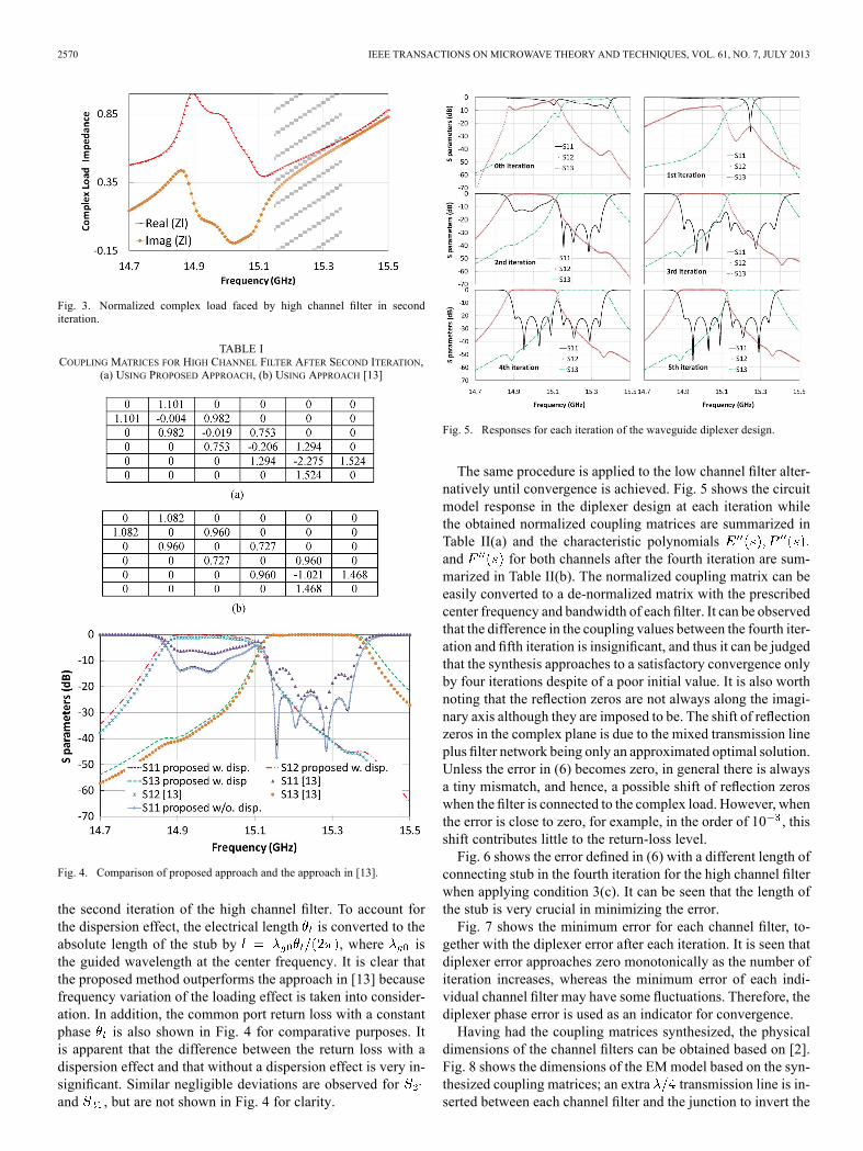
is below a certain threshold value, where the error of the thchannel is given by (6). Equivalently, the complex load faced byeach filter is iteratively adjusted until the matching error of eachfilter is small enough by adjusting the length of the intercon-necting stub. The center frequencies of the two channel filters inthis example are 15 and 15.25 GHz, respectively, the targeted re-turn loss is 22 dB, and the bandwidth is 0.2 GHz for both filters.The initial lengths of the stubs connected to the low channel andhigh channel are mm and mm, respec-tively. The frequency response of the waveguide T-junction isobtained through a full-wave mode-matching electromagnetic(EM) software. Initially, the coupling matrices for both filtersare generated by a conventional direct synthesis method with areal constant terminal impedance.Fig. 3 shows the complex load faced by the high channel
filter in the second iteration, normalized to the characteristicimpedance of a WR62 waveguide. Following the proce-dure given in Section II, the characteristic polynomials
and together with of the high channelfilter after the second iteration are given in Table I(a). Forcomparison, the synthesis approach [13] is repeated here withthe constant complex load of at
GHz.The obtained polynomials are reported in Table I(b). It can be
foreseen that when the complex load is a constant, only the I/Ocoupling and the self-coupling that are immediately next to theload get affected from that with the real load. Fig. 4 comparesthe synthesized diplexer responses using the proposed approach(including the dispersion effect) and the approach in [13] after
2570 IEEE TRANSACTIONS ON MICROWAVE THEORY AND TECHNIQUES, VOL. 61, NO. 7, JULY 2013
Fig. 3. Normalized complex load faced by high channel filter in seconditeration.
TABLE ICOUPLING MATRICES FOR HIGH CHANNEL FILTER AFTER SECOND ITERATION,
(a) USING PROPOSED APPROACH, (b) USING APPROACH [13]
Fig. 4. Comparison of proposed approach and the approach in [13].
the second iteration of the high channel filter. To account forthe dispersion effect, the electrical length is converted to theabsolute length of the stub by , where isthe guided wavelength at the center frequency. It is clear thatthe proposed method outperforms the approach in [13] becausefrequency variation of the loading effect is taken into consider-ation. In addition, the common port return loss with a constantphase is also shown in Fig. 4 for comparative purposes. Itis apparent that the difference between the return loss with adispersion effect and that without a dispersion effect is very in-significant. Similar negligible deviations are observed forand , but are not shown in Fig. 4 for clarity.
Fig. 5. Responses for each iteration of the waveguide diplexer design.
The same procedure is applied to the low channel filter alter-natively until convergence is achieved. Fig. 5 shows the circuitmodel response in the diplexer design at each iteration whilethe obtained normalized coupling matrices are summarized inTable II(a) and the characteristic polynomialsand for both channels after the fourth iteration are sum-marized in Table II(b). The normalized coupling matrix can beeasily converted to a de-normalized matrix with the prescribedcenter frequency and bandwidth of each filter. It can be observedthat the difference in the coupling values between the fourth iter-ation and fifth iteration is insignificant, and thus it can be judgedthat the synthesis approaches to a satisfactory convergence onlyby four iterations despite of a poor initial value. It is also worthnoting that the reflection zeros are not always along the imagi-nary axis although they are imposed to be. The shift of reflectionzeros in the complex plane is due to the mixed transmission lineplus filter network being only an approximated optimal solution.Unless the error in (6) becomes zero, in general there is alwaysa tiny mismatch, and hence, a possible shift of reflection zeroswhen the filter is connected to the complex load. However, whenthe error is close to zero, for example, in the order of 10 , thisshift contributes little to the return-loss level.Fig. 6 shows the error defined in (6) with a different length of
connecting stub in the fourth iteration for the high channel filterwhen applying condition 3(c). It can be seen that the length ofthe stub is very crucial in minimizing the error.Fig. 7 shows the minimum error for each channel filter, to-
gether with the diplexer error after each iteration. It is seen thatdiplexer error approaches zero monotonically as the number ofiteration increases, whereas the minimum error of each indi-vidual channel filter may have some fluctuations. Therefore, thediplexer phase error is used as an indicator for convergence.Having had the coupling matrices synthesized, the physical
dimensions of the channel filters can be obtained based on [2].Fig. 8 shows the dimensions of the EMmodel based on the syn-thesized coupling matrices; an extra transmission line is in-serted between each channel filter and the junction to invert the

MENG AND WU: DIRECT OPTIMAL SYNTHESIS OF MICROWAVE BANDPASS FILTER 2571
TABLE II(a) COUPLING MATRICES, INTERCONNECTING STUB LENGTH ANDMATCHING ERRORS FOR EACH ITERATION OF THE WAVEGUIDEDIPLEXER DESIGN EXAMPLE, (b) THE FINAL CHARACTERISTIC
POLYNOMIALS AFTER FOURTH ITERATION
phase of the physical filter since the phase of for a wave-guide filter at high frequency approaches to 180°, whereas thatdefined by characteristic polynomials approaches to 0°. In thephysical EM model, the thickness for all irises is 0.5 mm. The-parameters from the synthesized filter circuit model and thosefrom the EM designed model are compared in Fig. 9. The resultof the circuit model with a long waveguide at the center fre-quency inserted is identical to that of the EM designed model,
Fig. 6. Error versus interconnecting stub length at fourth iteration of highchannel.
Fig. 7. Errors versus number of iterations in diplexer design.
Fig. 8. Physical model of the designed -plane waveguide diplexer.
and therefore is not presented. The deviation between the resultsof the synthesized filter circuit model and that of the EM modelis introduced by the dispersive long waveguide. It is seenthat the proposed approach is more specified to filters with shuntLC resonators, whose reflection coefficient has a zero phase at
. For the filters with series LC resonators, on the otherhand, adding an extra transmission line will introduce a tol-erable error.It should be mentioned that the proposed method is only lim-
ited to noncontiguous cases in which the common port returnloss in the passband of each channel filter can be well approx-imated by the polynomials. When two channels are very close,e.g., less than 1% bandwidth, this assumption will be violated.Nevertheless, the solution by this method can still serve as agood initial point for further optimization.

2572 IEEE TRANSACTIONS ON MICROWAVE THEORY AND TECHNIQUES, VOL. 61, NO. 7, JULY 2013
Fig. 9. -parameters of synthesized circuit model and EM designed model ofan -plane waveguide diplexer.
Fig. 10. Circuit schematic of a coaxial resonator diplexer with a transmissionline Y-junction.
Fig. 11. Grounded wire line for realizing the transmission line between theY-junction and the coaxial resonator channel filters.
B. Coaxial Resonator Diplexer With a Wired Y-Junction
The design process of a coaxial combline diplexer consistingof a GSM channel and a CDMA channel is described in thisexample. The channel filters are connected to the common portthrough a grounded wire line Y-junction whose characteristicimpedances are , as illustrated inFig. 10. The characteristic impedance and are defined bythe grounded wire transmission line, as shown in Fig. 11, where
mm and the radius of conducting wire is 0.75 mm. Thechannel filters are initially designed as seventh order and 25-dBreturn loss by the conventional direct synthesis method withthe assumption that the terminated impedance is a real constantvalue. The center frequencies of channels 1 and 2 are 850 and940 MHz, respectively, and the bandwidths of both filters are55 MHz. A TZ at 910 MHz is prescribed for channel 1 and theother TZ is prescribed at 890MHz for channel 2. Initially andare arbitrarily selected to be mm and mm.Starting from the low channel filter, two channel filters are
synthesized alternatively by the proposed approach. The so-lution converges after two iterations. Since the characteristicimpedance at each port of the filter is different, those polyno-mials should be further renormalized to 125 . Table III showsthe coupling matrices obtained for both channels after re-nor-malization. The final interconnecting stub lengths are
TABLE IIICOUPLING MATRICES FOR THE COAXIAL DIPLEXER
Fig. 12. Photograph of the fabricated diplexer with top lid removed.
Fig. 13. -parameters of the synthesized and the measured responses of acoaxial resonator diplexer.
mm and mm. For validation purposes, thedesigned diplexer has been fabricated. The required positiveand negative cross-couplings are realized with capacitive andinductive probes, respectively. A photograph of the fabricateddiplexer is shown in Fig. 12. It can be seen that two designedsections of interconnecting stubs are realized using two piecesof wires extended from the Y-junction with the housing wallas the natural ground. Since the resonators are shunt LC type,there is no need to add an extra transmission line. Thefactor for both channel filters is about 2200. Finally, the mea-surement responses together with those from the synthesizeddiplexer circuit model are superimposed in Fig. 13. Good agree-ment demonstrates that the proposed approach can provide atrue realistic filter circuit model in practical applications.
MENG AND WU: DIRECT OPTIMAL SYNTHESIS OF MICROWAVE BANDPASS FILTER 2573
IV. CONCLUSION
A direct optimal synthesis method for a microwave bandpassfilter with a general loading effect is proposed in this paper. Twolegitimate assumptions are imposed: the prescribed TZs are sta-tionary when the load changes and the reflection zeros are dis-tributed along the imaginary axis of a complex frequency plane.By using the power wave renormalization, a set of conditions aredeveloped and used for determining a set of realistic and loaddependent objective polynomials, with which a new set of poly-nomials that describe the measurable filter responses of the tar-geted filter can be derived in accordance. It has been approvedthat this set of new polynomials can be very well approximatedby an ideal filter circuit model cascaded by a piece of transmis-sion line. The length of the transmission line is designed in anoptimal sense that the matching conditions are satisfied in a besteffort. The detailed design procedure is provided. The effective-ness of the proposedmethod has been demonstrated through twopractical design examples. It has been shown that the proposedapproach provides a robust and flexible design tool for the de-sign of a bandpass filter with a complex load.
REFERENCES[1] R. J. Cameron, “General coupling matrix synthesis methods for cheby-
shev filtering functions,” IEEE Trans. Microw. Theory Techn., vol. 47,no. 4, pp. 433–422, Apr. 1999.
[2] R. J. Cameron, C.M.Kudsia, and R. R.Mansour, Microwave Filters forCommunication Systems: Fundamentals, Design and Application.Hoboken, NJ, USA: Wiley, 2007, ch. 13, p. 494.
[3] M. Yu and Y.Wang, “Synthesis and beyond,” IEEEMicrow. Mag., vol.12, no. 6, pp. 62–76, Oct. 2011.
[4] R. J. Cameron and M. Yu, “Design of manifold-coupled multiplexers,”IEEE Microw. Mag., vol. 8, no. 5, pp. 46–59, Oct. 2007.
[5] M. Guglielmi, “Optimum CAD procedure for manifold diplexers,” inIEEE MTT-S Int. Microw. Symp. Dig., 1993, pp. 1081–1084.
[6] Y. Rong, H.-W. Yao, K. A. Zaki, and T. G. Dolan, “Millimeter-wave-band -plane diplexers and multiplexers,” IEEE Trans. Microw.
Theory Techn., vol. 47, no. 12, pp. 2325–2330, Dec. 1999.[7] A. Morini and T. Rozzi, “Constrains to the optimum performance and
bandwidth limitations of diplexers employing symmetric three-portjunctions,” IEEE Trans. Microw. Theory Techn., vol. 44, no. 2, pp.242–248, Feb. 1996.
[8] J. L. Haine and J. D. Rhodes, “Direct design formulas for asymmetricbandpass channel diplexer,” IEEE Trans. Microw. Theory Techn., vol.MTT-25, no. 10, pp. 807–814, Oct. 1977.
[9] J. D. Rhodes and R. Levy, “A generalized multiplexer theory,” IEEETrans. Microw. Theory Techn., vol. MTT-27, no. 2, pp. 99–111, Feb.1979.
[10] J. D. Rhodes and R. Levy, “Design of general manifold multiplexer,”IEEE Trans. Microw. Theory Techn., vol. MTT-27, no. 2, pp. 111–123,Feb. 1979.
[11] R. Levy, “Synthesis of non-contiguous diplexers using broadbandmatching theory,” in IEEE MTT-S Int. Microw. Symp. Dig., Boston,MA, USA, Jun. 10–14, 1991, pp. 543–546.
[12] G. Macchiarella and S. Tamiazzo, “Novel approach to the synthesis ofmicrowave diplexers,” IEEE Trans. Microw. Theory Techn., vol. 54,no. 12, pp. 4281–4290, Dec. 2006.
[13] K.-L. Wu and W. Meng, “A direct synthesis approach for microwavefilters with a complex load and its application to direct diplexer design,”IEEE Trans. Microw. Theory Techn., vol. 55, no. 5, pp. 1010–1017,May 2007.
[14] M. Meng and K.-L. Wu, “Direct synthesis of general Chebyshev band-pass filters with a frequency variant complex load,” in IEEE MTT-SInt. Microw. Symp. Dig., Anaheim, CA, USA, May 2010.
[15] K. Kurokawa, “Power waves and the scattering matrix,” IEEE Trans.Microw. Theory Techn., vol. MTT-13, no. 3, pp. 194–202, Mar. 1965.
[16] H. Meng and K.-L. Wu, “Direct optimal synthesis of microwave band-pass filters with a general loading effect,” in IEEE MTT-S Int. Microw.Symp. Dig., Montreal, QC, Canada, Jun. 2012.
[17] E. Kreyszig, Advanced Engineering Mathematics. New York, NY,USA: Wiley, 2005, ch. 20, pp. 860–862.
Huan Meng received the B.Eng. degree (withfirst-class honors) in electronic and informationengineering from The Hong Kong PolytechnicUniversity, Hung Hom, Hong Kong, in 2010, and theM.Phil. degree in electronic engineering from TheChinese University of Hong Kong, Shatin, HongKong, in 2012.Since 2012, he has been a Research Assistant
with the Department of Electronic Engineering, TheChinese University of Hong Kong. His researchis mainly focused on the design and synthesis of
passive microwave components, particularly microwave diplexers.Mr. Meng was the recipient of the Asia–Pacific Microwave Conference Prize
in 2012.
Ke-Li Wu (M’90–SM’96–F’11) received the B.S.and M.Eng. degrees from the Nanjing University ofScience and Technology, Nanjing, China, in 1982and 1985, respectively, and the Ph.D. degree fromLaval University, Quebec, QC, Canada, in 1989.From 1989 to 1993, he was with the Communica-
tions Research Laboratory, McMaster University, asa Research Engineer and a GroupManager. In March1993, he joined the Corporate Research and Develop-ment Division, COM DEV International (the largestCanadian space equipment manufacturer), where he
was a Principal Member of Technical Staff. Since October 1999, he has beenwith The Chinese University of Hong Kong, Shatin, Hong Kong, where he iscurrently a Professor and the Director of the Radiofrequency Radiation Re-search Laboratory (R3L). He has authored or coauthored numerous publica-tions in the areas of electromagnetic (EM) modeling and microwave passivecomponents, microwave filters, and antenna engineering. His current researchinterests include partial element equivalent circuit (PEEC) and derived physi-cally expressive circuit (DPEC) EM modeling of high-speed circuits, RF andmicrowave passive circuits and systems, synthesis theory and practices of mi-crowave filters, antennas for wireless terminals, low-temperature co-fired ce-ramic (LTCC)-based multichip modules (MCMs), and RF identification (RFID)technologies. His research group is the main workforce in various active RFIDresearch and applications in Hong Kong.Prof. Wu is a member of the IEEEMTT-8 Subcommittee (Filters and Passive
Components). He serves as a Technical Program Committee (TPC) memberfor many prestigious international conferences including the IEEE MicrowaveTheory and Techniques Society (IEEE MTT-S) International MicrowaveSymposium (IMS). He was an associate editor for the IEEE TRANSACTIONSON MICROWAVE THEORY AND TECHNIQUES (2006–2009). He was the recipientof the 1998 COM DEV Achievement Award for the development of exact EMdesign software of microwave filters and multiplexers and the Asia–PacificMicrowave Conference Prize in 2008 and 2012.