256 DS-5 ARM DSTREAM System and Interface Design...
59
ARM ® DS-5 Version 5 ARM DSTREAM System and Interface Design Reference Guide Copyright © 2010-2012, 2015, 2016 ARM. All rights reserved. ARM DUI0499K
Transcript of 256 DS-5 ARM DSTREAM System and Interface Design...

ARM® DS-5Version 5
ARM DSTREAM System and Interface Design ReferenceGuide
Copyright © 2010-2012, 2015, 2016 ARM. All rights reserved.ARM DUI0499K

ARM® DS-5ARM® DSTREAM System and Interface Design Reference GuideCopyright © 2010-2012, 2015, 2016 ARM. All rights reserved.
Release Information
Document History
Issue Date Confidentiality Change
A May 2010 Non-Confidential First release
B November 2010 Non-Confidential Update for DS-5 version 5.3
C 30 April 2011 Non-Confidential Update for DSTREAM and RVI v4.2.1
D 29 July 2011 Non-Confidential Update for DS-5 version 5.6
E 30 September 2011 Non-Confidential Update for DSTREAM and RVI v4.4, and DS-5 version 5.7
F 29 February 2012 Non-Confidential Update for DS-5 version 5.9
G 29 July 2012 Non-Confidential Update for DS-5 version 5.11
H 12 October 2012 Non-Confidential Update for DS-5 version 5.12
I 20 March 2015 Non-Confidential Update for DS-5 version 5.21
J 15 July 2015 Non-Confidential Update for DS-5 version 5.22
K 15 March 2016 Non-Confidential Update for DS-5 version 5.24
Non-Confidential Proprietary Notice
This document is protected by copyright and other related rights and the practice or implementation of the information contained inthis document may be protected by one or more patents or pending patent applications. No part of this document may bereproduced in any form by any means without the express prior written permission of ARM. No license, express or implied, byestoppel or otherwise to any intellectual property rights is granted by this document unless specifically stated.
Your access to the information in this document is conditional upon your acceptance that you will not use or permit others to usethe information for the purposes of determining whether implementations infringe any third party patents.
THIS DOCUMENT IS PROVIDED “AS IS”. ARM PROVIDES NO REPRESENTATIONS AND NO WARRANTIES,EXPRESS, IMPLIED OR STATUTORY, INCLUDING, WITHOUT LIMITATION, THE IMPLIED WARRANTIES OFMERCHANTABILITY, SATISFACTORY QUALITY, NON-INFRINGEMENT OR FITNESS FOR A PARTICULAR PURPOSEWITH RESPECT TO THE DOCUMENT. For the avoidance of doubt, ARM makes no representation with respect to, and hasundertaken no analysis to identify or understand the scope and content of, third party patents, copyrights, trade secrets, or otherrights.
This document may include technical inaccuracies or typographical errors.
TO THE EXTENT NOT PROHIBITED BY LAW, IN NO EVENT WILL ARM BE LIABLE FOR ANY DAMAGES,INCLUDING WITHOUT LIMITATION ANY DIRECT, INDIRECT, SPECIAL, INCIDENTAL, PUNITIVE, ORCONSEQUENTIAL DAMAGES, HOWEVER CAUSED AND REGARDLESS OF THE THEORY OF LIABILITY, ARISINGOUT OF ANY USE OF THIS DOCUMENT, EVEN IF ARM HAS BEEN ADVISED OF THE POSSIBILITY OF SUCHDAMAGES.
This document consists solely of commercial items. You shall be responsible for ensuring that any use, duplication or disclosure ofthis document complies fully with any relevant export laws and regulations to assure that this document or any portion thereof isnot exported, directly or indirectly, in violation of such export laws. Use of the word “partner” in reference to ARM’s customers isnot intended to create or refer to any partnership relationship with any other company. ARM may make changes to this document atany time and without notice.
If any of the provisions contained in these terms conflict with any of the provisions of any signed written agreement covering thisdocument with ARM, then the signed written agreement prevails over and supersedes the conflicting provisions of these terms.This document may be translated into other languages for convenience, and you agree that if there is any conflict between theEnglish version of this document and any translation, the terms of the English version of the Agreement shall prevail.
ARM® DS-5
ARM DUI0499K Copyright © 2010-2012, 2015, 2016 ARM. All rights reserved. 2Non-Confidential
Words and logos marked with ® or ™ are registered trademarks or trademarks of ARM Limited or its affiliates in the EU and/orelsewhere. All rights reserved. Other brands and names mentioned in this document may be the trademarks of their respectiveowners. Please follow ARM’s trademark usage guidelines at http://www.arm.com/about/trademark-usage-guidelines.php
Copyright © [2010-2012, 2015, 2016], ARM Limited or its affiliates. All rights reserved.
ARM Limited. Company 02557590 registered in England.
110 Fulbourn Road, Cambridge, England CB1 9NJ.
LES-PRE-20349
Confidentiality Status
This document is Non-Confidential. The right to use, copy and disclose this document may be subject to license restrictions inaccordance with the terms of the agreement entered into by ARM and the party that ARM delivered this document to.
Unrestricted Access is an ARM internal classification.
Product Status
The information in this document is Final, that is for a developed product.
Web Address
http://www.arm.com
Conformance NoticesThis section contains conformance notices.
Federal Communications Commission NoticeThis device is test equipment and consequently is exempt from part 15 of the FCC Rules under section 15.103 (c).
Class AImportant: This is a Class A device. In residential areas, this device may cause radio interference. The user should take thenecessary precautions, if appropriate.
CE Declaration of Conformity
The system should be powered down when not in use.
It is recommended that ESD precautions be taken when handling DSTREAM, RVI, and RVT equipment.
The DSTREAM, RVI, and RVT modules generate, use, and can radiate radio frequency energy and may cause harmful interferenceto radio communications. There is no guarantee that interference will not occur in a particular installation. If this equipment causesharmful interference to radio or television reception, which can be determined by turning the equipment off or on, you areencouraged to try to correct the interference by one or more of the following measures:
• ensure attached cables do not lie across the target board• reorient the receiving antenna• increase the distance between the equipment and the receiver• connect the equipment into an outlet on a circuit different from that to which the receiver is connected• consult the dealer or an experienced radio/TV technician for help
Note
It is recommended that wherever possible shielded interface cables be used.
ARM® DS-5
ARM DUI0499K Copyright © 2010-2012, 2015, 2016 ARM. All rights reserved. 3Non-Confidential

ContentsARM® DS-5 ARM DSTREAM System and InterfaceDesign Reference Guide
PrefaceAbout this book ..................................................... ..................................................... 10
Chapter 1 ARM DSTREAM System Design Guidelines1.1 About adaptive clocking to synchronize the JTAG port ..................... ..................... 1-131.2 Reset signals ..................................................... ..................................................... 1-161.3 ASIC guidelines ................................................... ................................................... 1-181.4 PCB guidelines ........................................................................................................ 1-20
Chapter 2 ARM DSTREAM Target Interface Connections2.1 Signal descriptions ................................................. ................................................. 2-232.2 Target connectors supported by DSTREAM ............................................................ 2-272.3 The Mictor 38 connector pinouts and interface signals ..................... ..................... 2-282.4 The ARM JTAG 20 connector pinouts and interface signals ................. ................. 2-322.5 The TI JTAG 14 connector pinouts and interface signals ........................................ 2-352.6 The ARM JTAG 14 connector pinouts and interface signals ................. ................. 2-372.7 The CoreSight 10 connector pinouts and interface signals .................. .................. 2-392.8 The CoreSight 20 connector pinouts and interface signals .................. .................. 2-412.9 The MIPI 34 connector pinouts and interface signals .............................................. 2-442.10 I/O diagrams for the DSTREAM probe connectors ........................ ........................ 2-482.11 Voltage domains of the DSTREAM probe ............................... ............................... 2-502.12 Series termination .................................................................................................... 2-51
ARM DUI0499K Copyright © 2010-2012, 2015, 2016 ARM. All rights reserved. 4Non-Confidential

Chapter 3 ARM DSTREAM User I/O Connections3.1 About the User I/O connector .................................................................................. 3-533.2 User I/O pin connections ............................................ ............................................ 3-54
Chapter 4 Target Board Design for Tracing with ARM DSTREAM4.1 Overview of high-speed design ....................................... ....................................... 4-564.2 PCB track impedance .............................................................................................. 4-574.3 Signal requirements ................................................ ................................................ 4-584.4 Probe modeling ................................................... ................................................... 4-59
ARM DUI0499K Copyright © 2010-2012, 2015, 2016 ARM. All rights reserved. 5Non-Confidential

List of FiguresARM® DS-5 ARM DSTREAM System and InterfaceDesign Reference Guide
Figure 1-1 Basic JTAG port synchronizer ............................................................................................... 1-14Figure 1-2 Timing diagram for the Basic JTAG synchronizer .................................................................. 1-14Figure 1-3 JTAG port synchronizer for single rising-edge D-type ASIC design rules ............................. 1-14Figure 1-4 Timing diagram for the D-type JTAG synchronizer ................................................................ 1-15Figure 1-5 Example reset circuit logic ..................................................................................................... 1-17Figure 1-6 TAP Controllers serially chained within an ASIC ................................................................... 1-18Figure 1-7 Typical PCB connections ....................................................................................................... 1-20Figure 1-8 Target interface logic levels ................................................................................................... 1-21Figure 2-1 JTAG port timing diagram ...................................................................................................... 2-23Figure 2-2 Typical SWD connections ...................................................................................................... 2-24Figure 2-3 SWD timing diagrams ............................................................................................................ 2-25Figure 2-4 Clock waveforms ................................................................................................................... 2-26Figure 2-5 Mictor 38 connector pinout .................................................................................................... 2-28Figure 2-6 ARM JTAG 20 connector pinout ............................................................................................ 2-32Figure 2-7 TI JTAG 14 connector pinout ................................................................................................. 2-35Figure 2-8 ARM JTAG 14 connector pinout ............................................................................................ 2-37Figure 2-9 CoreSight 10 connector pinout .............................................................................................. 2-39Figure 2-10 CoreSight 20 connector pinout .............................................................................................. 2-41Figure 2-11 MIPI 34 connector pinout ....................................................................................................... 2-44Figure 2-12 Input ....................................................................................................................................... 2-48Figure 2-13 Output .................................................................................................................................... 2-48Figure 2-14 Input/Output ........................................................................................................................... 2-48
ARM DUI0499K Copyright © 2010-2012, 2015, 2016 ARM. All rights reserved. 6Non-Confidential

Figure 2-15 Reset output .......................................................................................................................... 2-48Figure 2-16 Reset output with feedback ................................................................................................... 2-48Figure 2-17 VTRef input ............................................................................................................................ 2-49Figure 2-18 VTRef input (decoupled) ........................................................................................................ 2-49Figure 2-19 Ground ................................................................................................................................... 2-49Figure 2-20 AC Ground ............................................................................................................................. 2-49Figure 3-1 User I/O pin connections ....................................................................................................... 3-53Figure 4-1 Track impedance ................................................................................................................... 4-57Figure 4-2 Data waveforms ..................................................................................................................... 4-58
ARM DUI0499K Copyright © 2010-2012, 2015, 2016 ARM. All rights reserved. 7Non-Confidential
List of TablesARM® DS-5 ARM DSTREAM System and InterfaceDesign Reference Guide
Table 2-1 DSTREAM JTAG Characteristics .......................................................................................... 2-24Table 2-2 SWD timing requirements ...................................................................................................... 2-25Table 2-3 TRACECLK frequencies ........................................................................................................ 2-26Table 2-4 Mictor 38 interface pinout table ............................................................................................. 2-29Table 2-5 Mictor 38 signals .................................................................................................................... 2-30Table 2-6 ARM JTAG 20 interface pinout table ..................................................................................... 2-32Table 2-7 ARM JTAG 20 signals ............................................................................................................ 2-33Table 2-8 TI JTAG 14 interface pinout table .......................................................................................... 2-35Table 2-9 TI JTAG 14 signals ................................................................................................................ 2-36Table 2-10 ARM JTAG 14 interface pinout table ..................................................................................... 2-37Table 2-11 ARM JTAG 14 signals ............................................................................................................ 2-38Table 2-12 CoreSight 10 interface pinout table ....................................................................................... 2-39Table 2-13 CoreSight 10 signals ............................................................................................................. 2-40Table 2-14 CoreSight 20 interface pinout table ....................................................................................... 2-42Table 2-15 CoreSight 20 signals ............................................................................................................. 2-42Table 2-16 MIPI 34 interface pinout table ................................................................................................ 2-45Table 2-17 MIPI 34 signals ...................................................................................................................... 2-46Table 2-18 Typical series terminating resistor values .............................................................................. 2-51Table 3-1 User I/O pin connections ....................................................................................................... 3-54Table 4-1 Data setup and hold .............................................................................................................. 4-58
ARM DUI0499K Copyright © 2010-2012, 2015, 2016 ARM. All rights reserved. 8Non-Confidential

Preface
This preface introduces the ARM® DS-5 ARM DSTREAM System and Interface Design Reference Guide.
It contains the following:• About this book on page 10.
ARM DUI0499K Copyright © 2010-2012, 2015, 2016 ARM. All rights reserved. 9Non-Confidential

About this bookDSTREAM System and Interface Design Reference Guide describes the DSTREAM debug and traceunit, with details about designing ARM® architecture-based ASICs and PCBs. This document is writtenfor those using DSTREAM with DS-5 Debugger, and is available as a PDF.
Using this book
This book is organized into the following chapters:
Chapter 1 ARM DSTREAM System Design GuidelinesThis contains information on developing ARM® architecture-based devices and Printed CircuitBoards (PCBs) that can be debugged using ARM DSTREAM™.
Chapter 2 ARM DSTREAM Target Interface ConnectionsThis describes the interface connections on the DSTREAM unit.
Chapter 3 ARM DSTREAM User I/O ConnectionsThis describes the additional input and output connections provided in DSTREAM.
Chapter 4 Target Board Design for Tracing with ARM DSTREAMThis describes the properties of a target board that can be connected to the DSTREAM tracefeature.
Glossary
The ARM Glossary is a list of terms used in ARM documentation, together with definitions for thoseterms. The ARM Glossary does not contain terms that are industry standard unless the ARM meaningdiffers from the generally accepted meaning.
See the ARM Glossary for more information.
Typographic conventions
italicIntroduces special terminology, denotes cross-references, and citations.
boldHighlights interface elements, such as menu names. Denotes signal names. Also used for termsin descriptive lists, where appropriate.
monospaceDenotes text that you can enter at the keyboard, such as commands, file and program names,and source code.
monospaceDenotes a permitted abbreviation for a command or option. You can enter the underlined textinstead of the full command or option name.
monospace italicDenotes arguments to monospace text where the argument is to be replaced by a specific value.
monospace boldDenotes language keywords when used outside example code.
<and>Encloses replaceable terms for assembler syntax where they appear in code or code fragments.For example:
MRC p15, 0, <Rd>, <CRn>, <CRm>, <Opcode_2>
SMALL CAPITALS
Used in body text for a few terms that have specific technical meanings, that are defined in theARM glossary. For example, IMPLEMENTATION DEFINED, IMPLEMENTATION SPECIFIC, UNKNOWN, andUNPREDICTABLE.
Feedback
Preface About this book
ARM DUI0499K Copyright © 2010-2012, 2015, 2016 ARM. All rights reserved. 10Non-Confidential
Feedback on this product
If you have any comments or suggestions about this product, contact your supplier and give:• The product name.• The product revision or version.• An explanation with as much information as you can provide. Include symptoms and diagnostic
procedures if appropriate.
Feedback on content
If you have comments on content then send an e-mail to [email protected]. Give:
• The title ARM® DS-5 ARM DSTREAM System and Interface Design Reference Guide.• The number ARM DUI0499K.• If applicable, the page number(s) to which your comments refer.• A concise explanation of your comments.
ARM also welcomes general suggestions for additions and improvements. Note
ARM tests the PDF only in Adobe Acrobat and Acrobat Reader, and cannot guarantee the quality of therepresented document when used with any other PDF reader.
Other information
• ARM Information Center.• ARM Technical Support Knowledge Articles.• Support and Maintenance.• ARM Glossary.
Preface About this book
ARM DUI0499K Copyright © 2010-2012, 2015, 2016 ARM. All rights reserved. 11Non-Confidential
Chapter 1ARM DSTREAM System Design Guidelines
This contains information on developing ARM® architecture-based devices and Printed Circuit Boards(PCBs) that can be debugged using ARM DSTREAM™.
It contains the following sections:• 1.1 About adaptive clocking to synchronize the JTAG port on page 1-13.• 1.2 Reset signals on page 1-16.• 1.3 ASIC guidelines on page 1-18.• 1.4 PCB guidelines on page 1-20.
ARM DUI0499K Copyright © 2010-2012, 2015, 2016 ARM. All rights reserved. 1-12Non-Confidential

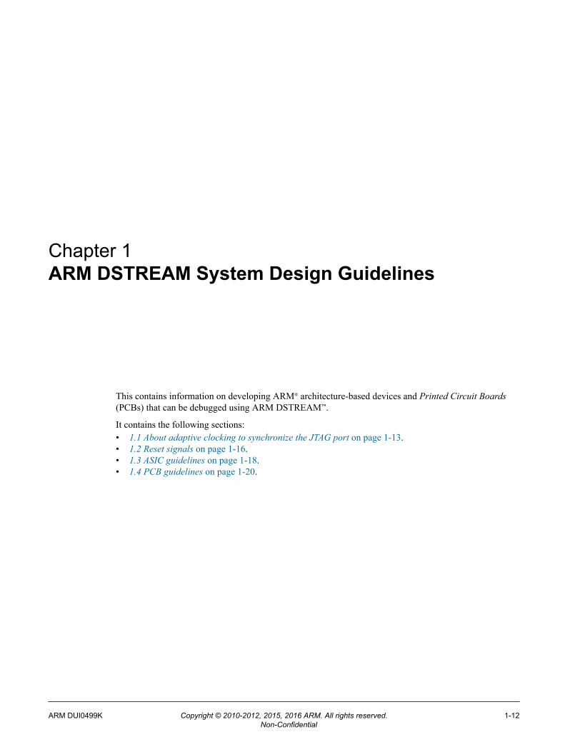
1.1 About adaptive clocking to synchronize the JTAG portARM architecture-based devices that use only hard macrocells, such as ARM7TDMI® and ARM920T,use the standard five-wire JTAG interface. However, some target systems require that JTAG events aresynchronized to a clock in the system. The adaptive clocking feature of DSTREAM addresses thisrequirement.
The standard five-wire JTAG interface comprises the TCK, TMS, TDI, TDO, and nTRST signals. Toensure a valid JTAG CLK setting, systems that require the JTAG events to be synchronized to a clock inthe system often support an extra signal (RTCK) at the JTAG port:
• An Application-Specific Integrated Circuit (ASIC) with single rising-edge D-type design rules, suchas one based on an ARM7TDMI-S™ processor.
• A system where scan chains external to the ARM macrocell must meet single rising-edge D-typedesign rules.
When adaptive clocking is enabled, DSTREAM issues a TCK signal and waits for the RTCK signal tocome back. DSTREAM does not progress to the next TCK until RTCK is received.
Note
• Adaptive clocking is automatically configured in ARM DS-5™ as required by the target.• If you use the adaptive clocking feature, transmission delays, gate delays, and synchronization
requirements result in a lower maximum clock frequency than with non-adaptive clocking. Do notuse adaptive clocking unless it is required by the hardware design.
• If, when autoconfiguring a target, the DSTREAM unit receives pulses on RTCK in response to TCKit assumes that adaptive clocking is required, and enables adaptive clocking in the targetconfiguration. If the hardware does not require adaptive clocking, the target is driven slower than itcould be. You can disable adaptive clocking using controls on the JTAG settings dialog box.
• If adaptive clocking is used, DSTREAM cannot detect the clock speed, and therefore cannot scale itsinternal timeouts. If the target clock frequency is very slow, a JTAG timeout might occur. This leavesthe JTAG in an unknown state, and DSTREAM cannot operate correctly without reconnecting to theprocessor. JTAG timeouts are enabled by default. You can disable JTAG timeouts by deselecting theoption JTAG Timeouts Enabled in the installed Debug Hardware Config utility provided with theDSTREAM unit.
You can use adaptive clocking as an interface to targets with slow or widely varying clock frequency,such as battery-powered equipment that varies its clock speed according to processing demand. In thissystem, TCK might be hundreds of times faster than the system clock, and the debugger losessynchronization with the target system. Adaptive clocking ensures that the JTAG port speedautomatically adapts to slow system speed.
The following figure shows a circuit for a basic JTAG port synchronizer.
1 ARM DSTREAM System Design Guidelines1.1 About adaptive clocking to synchronize the JTAG port
ARM DUI0499K Copyright © 2010-2012, 2015, 2016 ARM. All rights reserved. 1-13Non-Confidential
nTRST
CLK
TCK
TDO
TMO
TDI
ASIC
nCLRD Q D Q
nCLR
RTCK
TDO
TCK
nTRST
CLK
TMS
TDI
Figure 1-1 Basic JTAG port synchronizer
The following figure shows a partial timing diagram for the basic JTAG synchronizer. The delay can bereduced by clocking the flip-flops from opposite edges of the system clock, because the second flip-floponly provides better immunity to metastability problems. Even a single flip-flop synchronizer nevercompletely misses TCK events, because RTCK is part of a feedback loop controlling TCK.
CLK
TCK
RTCK
Figure 1-2 Timing diagram for the Basic JTAG synchronizer
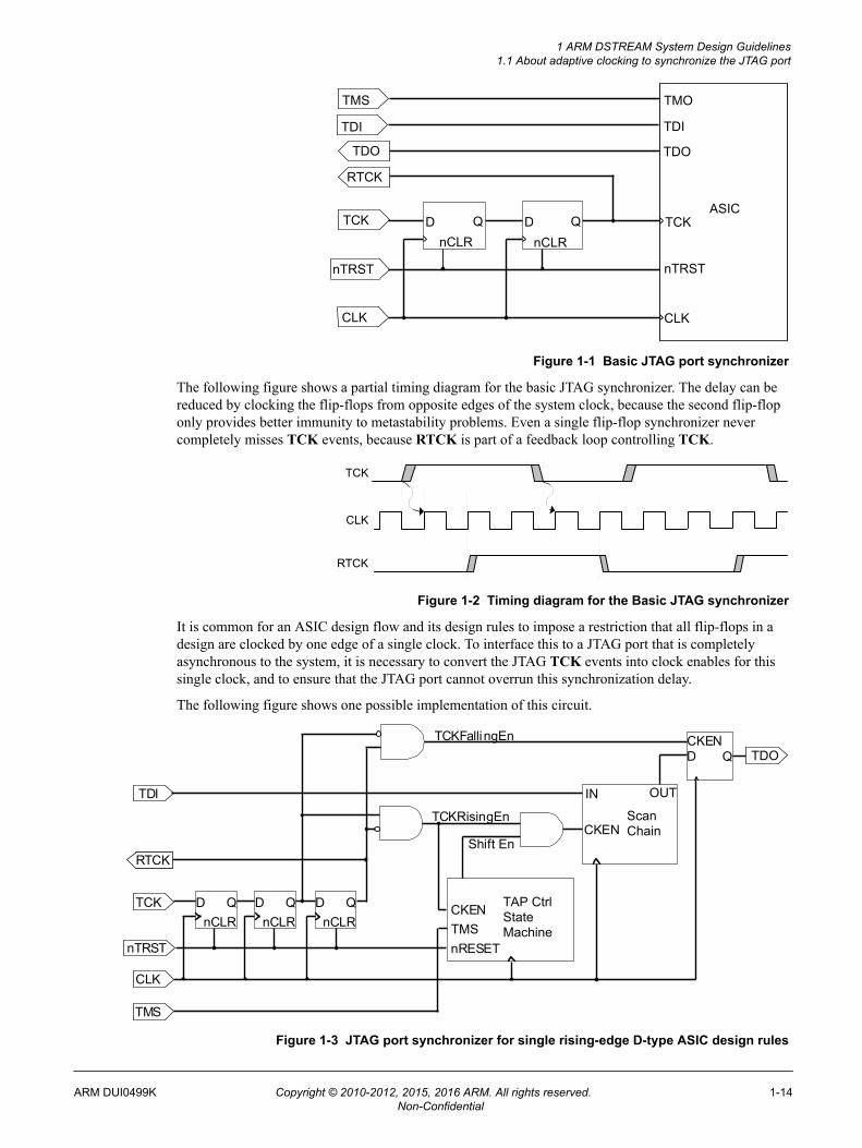
It is common for an ASIC design flow and its design rules to impose a restriction that all flip-flops in adesign are clocked by one edge of a single clock. To interface this to a JTAG port that is completelyasynchronous to the system, it is necessary to convert the JTAG TCK events into clock enables for thissingle clock, and to ensure that the JTAG port cannot overrun this synchronization delay.
The following figure shows one possible implementation of this circuit.
CKEN
IN
nRESETTMSCKEN TAP Ctrl
StateMachine
OUT
ScanChain
CKENTCKFallingEn
TCKRisingEn
Shift En
D Q
nCLRD Q
nCLRD Q
nCLRD Q
TDO
TMS
CLK
nTRST
TCK
RTCK
TDI
Figure 1-3 JTAG port synchronizer for single rising-edge D-type ASIC design rules
1 ARM DSTREAM System Design Guidelines1.1 About adaptive clocking to synchronize the JTAG port
ARM DUI0499K Copyright © 2010-2012, 2015, 2016 ARM. All rights reserved. 1-14Non-Confidential
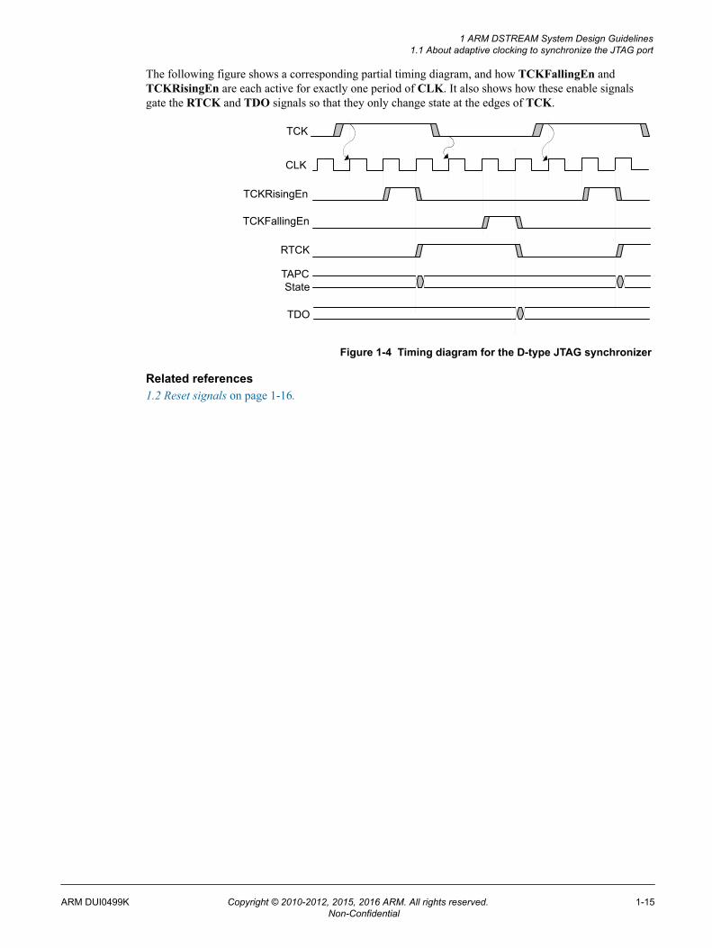
The following figure shows a corresponding partial timing diagram, and how TCKFallingEn andTCKRisingEn are each active for exactly one period of CLK. It also shows how these enable signalsgate the RTCK and TDO signals so that they only change state at the edges of TCK.
CLK
TCKRisingEn
TCK
TCKFallingEn
RTCK
TAPC State
TDO
Figure 1-4 Timing diagram for the D-type JTAG synchronizer
Related references1.2 Reset signals on page 1-16.
1 ARM DSTREAM System Design Guidelines1.1 About adaptive clocking to synchronize the JTAG port
ARM DUI0499K Copyright © 2010-2012, 2015, 2016 ARM. All rights reserved. 1-15Non-Confidential

1.2 Reset signalsThere are two types of reset signals available on ARM devices. DSTREAM expects these signals to bewired in a certain way.
This section contains the following subsections:• 1.2.1 ARM reset signals on page 1-16.• 1.2.2 DSTREAM reset signals on page 1-16.• 1.2.3 Example reset circuits on page 1-17.
1.2.1 ARM reset signals
All ARM processors have a main processor reset that might be called nRESET, BnRES, or HRESET.
This is asserted by one or more of these conditions:
• Power on.• Manual push button.• Remote reset from the debugger (using DSTREAM).• Watchdog circuit (if appropriate to the application).
Any ARM processor including the JTAG interface has a second reset input called nTRST (TAP Reset).This resets the EmbeddedICE logic, the Test Access Port (TAP) controller, and the boundary scan cells. Itis activated by remote JTAG reset (from DSTREAM).
ARM strongly recommends that both signals are separately available on the JTAG connector. If thenRESET and nTRST signals are linked together, resetting the system also resets the TAP controller.This means that:• It is not possible to debug a system from reset, because any breakpoints previously set are lost.• You might have to start the debug session from the beginning, because DSTREAM might not recover
when the TAP controller state is changed.
Related references1.2.2 DSTREAM reset signals on page 1-16.1.2.3 Example reset circuits on page 1-17.
1.2.2 DSTREAM reset signals
The DSTREAM unit has two reset signals connected to the debug target hardware, nTRST and nSRST.
What the signals do:• nTRST drives the JTAG nTRST signal on the ARM processor. It is an output that is activated
whenever the debug software has to re-initialize the debug interface in the target system.• nSRST is a bidirectional signal that both drives and senses the system reset signal on the target. By
default, this output is driven LOW by the debugger to re-initialize the target system.
The target hardware must pull the reset lines to their inactive state to assure normal operation when theJTAG interface is disconnected. In the DSTREAM unit, the strong pull-up/pull-down resistance isapproximately 33Ω, and the weak pull-up/pull-down resistance is approximately 4.7kΩ. Because you canselect the drive strength for nTRST and nSRST, target assemblies with a variey of different resetconfigurations can be supported.
Related references1.2.1 ARM reset signals on page 1-16.1.2.3 Example reset circuits on page 1-17.
Related informationDebug hardware Advanced configuration reset options.
1 ARM DSTREAM System Design Guidelines1.2 Reset signals
ARM DUI0499K Copyright © 2010-2012, 2015, 2016 ARM. All rights reserved. 1-16Non-Confidential

1.2.3 Example reset circuits
The diagram shows a typical reset circuit logic for the ARM reset signals and the DSTREAM resetsignals.
TRST
RESET
RST
RST
GndGnd
ARMprocessor
VDD
VDD
TAP RESET
SYSTEM RESET
Open-drainreset devicese.g. STM1001
To otherlogic
VDD
VDD
nTRST
nSRST
Manualreset
10K
10K
100R100nF
Sig
nals
from
JTA
G c
onne
ctor
Figure 1-5 Example reset circuit logic
Related references1.2.1 ARM reset signals on page 1-16.1.2.2 DSTREAM reset signals on page 1-16.
1 ARM DSTREAM System Design Guidelines1.2 Reset signals
ARM DUI0499K Copyright © 2010-2012, 2015, 2016 ARM. All rights reserved. 1-17Non-Confidential

1.3 ASIC guidelinesThis provides guidelines for ASIC designs.
This section contains the following subsections:• 1.3.1 ICs containing multiple devices on page 1-18.• 1.3.2 Boundary scan test vectors on page 1-19.
1.3.1 ICs containing multiple devices
If your ASIC contains multiple devices that have a JTAG Test Access Port (TAP) controller, you mustserially chain them so that DSTREAM can communicate with all of them simultaneously. The chainingcan either be within the ASIC, or externally.
Note
There is no support in DSTREAM for multiplexing TCK, TMS, TDI, TDO, and RTCK between anumber of different processors.
TAP controllers serially chained within the ASIC
The JTAG standard originally described serially chaining multiple devices on a PCB. This concept canbe extended to serially chaining multiple TAP controllers within an ASIC, as shown in the followingfigure:
TDI
TDI TDOTAP
Controller
TCK
nTRST
TMS
TDO
TDI
Second Tap Device
TDO
TCKnTRSTTMS
TCKnTRSTTMS
TAPController
First Tap Device
Figure 1-6 TAP Controllers serially chained within an ASIC
This configuration does not increase the package pin count. It does increase JTAG propagation delays,but this impact can be small if you put unaddressed TAP controllers into bypass mode.
TAP controllers serially chained externally
You can use separate pins on the ASIC for each JTAG port, and serially chain them externally (forexample on the PCB). This configuration can simplify device testing, and gives the greatest flexibility onthe PCB. However, this is at the cost of many pins on the device package.
Related concepts1.3.2 Boundary scan test vectors on page 1-19.
1 ARM DSTREAM System Design Guidelines1.3 ASIC guidelines
ARM DUI0499K Copyright © 2010-2012, 2015, 2016 ARM. All rights reserved. 1-18Non-Confidential
Related informationCoreSight Technology System Design Guide.
1.3.2 Boundary scan test vectors
If you use the JTAG boundary scan test methodology to apply production test vectors, you might want tohave independent external access to each Test Access Port (TAP) controller. This avoids the requirementto merge test vectors for more than one block in the device.
One solution to this is to adopt a hybrid, using a pin on the package that switches elements of the deviceinto a test mode. You can use this to break the internal daisy chaining of TDO and TDI signals, and tomultiplex out independent JTAG ports on pins that are used for another purpose during normal operation.
Related concepts1.3.1 ICs containing multiple devices on page 1-18.
Related informationCoreSight Technology System Design Guide.
1 ARM DSTREAM System Design Guidelines1.3 ASIC guidelines
ARM DUI0499K Copyright © 2010-2012, 2015, 2016 ARM. All rights reserved. 1-19Non-Confidential

1.4 PCB guidelinesThis provides PCB guidelines on the physical and electrical connections present on the target board.
This section contains the following subsections:• 1.4.1 PCB connections on page 1-20.• 1.4.2 Target interface logic levels on page 1-20.
1.4.1 PCB connections
The diagram shows a typical JTAG connection scheme.
TRSTRESET
ARMProcessor/
ASIC
10KS
igna
ls fr
om J
TAG
con
nect
or
TDITMSTCKRTCKTDO
DBGRQDBGACK
10K
Gnd Gnd
Resetcircuit
22R22R
0R 10K
10K
10K
10K
10K
VDD
Gnd
VTREFTDITMSTCK
RTCK
nTRSTnSRST
DBGRQ
TDO
DBGACK
GND
Figure 1-7 Typical PCB connections
Note
• The signals TDI, TMS, TCK, RTCK and TDO are typically pulled up on the target board to keepthem stable when the debug equipment is not connected.
• DBGRQ and DBGACK are typically pulled down on the target.• If there is no RTCK signal provided on the processor, it can either be pulled to a fixed logic level or
connected to the TCK signal to provide a direct loop-back.• All pull-up and pull-down resistors must be in the range 1K-100KΩ.• The VTREF signal is typically connected directly to the VDD rail. If you use a series resistor to
protect against short-circuits, it must have a value no greater than 100Ω.• To improve signal integrity, it is good practice to provide an impedance matching resistor on the
TDO and RTCK outputs of the processor. The value of these resistors, added to the impedance of thedriver must be approximately equal to 50Ω.
Related references1.3 ASIC guidelines on page 1-18.1.4.2 Target interface logic levels on page 1-20.
1.4.2 Target interface logic levels
DSTREAM is designed to interface with a wide range of target system logic levels. It does this byadapting its output drive and input threshold to a reference voltage supplied by the target system.
1 ARM DSTREAM System Design Guidelines1.4 PCB guidelines
ARM DUI0499K Copyright © 2010-2012, 2015, 2016 ARM. All rights reserved. 1-20Non-Confidential
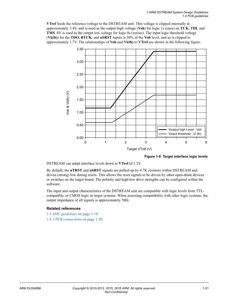
VTref feeds the reference voltage to the DSTREAM unit. This voltage is clipped internally atapproximately 3.4V, and is used as the output high voltage (Voh) for logic 1s (ones) on TCK, TDI, andTMS. 0V is used as the output low voltage for logic 0s (zeroes). The input logic threshold voltage(Vi(th)) for the TDO, RTCK, and nSRST inputs is 50% of the Voh level, and so is clipped toapproximately 1.7V. The relationships of Voh and Vi(th) to VTref are shown in the following figure:
0.00
0.50
1.00
1.50
2.00
2.50
3.00
3.50
0 1 2 3 4 5 6
Target VTref (V)
Voh
& V
i(th)
(V)
Voutput high Level - VohVinput threshold - Vi (th)
Figure 1-8 Target interface logic levels
DSTREAM can adapt interface levels down to VTref of 1.2V.
By default, the nTRST and nSRST signals are pulled-up by 4.7K resistors within DSTREAM anddriven (strong) low during resets. This allows the reset signals to be driven by other open-drain devicesor switches on the target board. The polarity and high/low drive strengths can be configured within thesoftware.
The input and output characteristics of the DSTREAM unit are compatible with logic levels from TTL-compatible, or CMOS logic in target systems. When assessing compatibility with other logic systems, theoutput impedance of all signals is approximately 50Ω.
Related references1.3 ASIC guidelines on page 1-18.1.4.1 PCB connections on page 1-20.
1 ARM DSTREAM System Design Guidelines1.4 PCB guidelines
ARM DUI0499K Copyright © 2010-2012, 2015, 2016 ARM. All rights reserved. 1-21Non-Confidential

Chapter 2ARM DSTREAM Target Interface Connections
This describes the interface connections on the DSTREAM unit.
It contains the following sections:• 2.1 Signal descriptions on page 2-23.• 2.2 Target connectors supported by DSTREAM on page 2-27.• 2.3 The Mictor 38 connector pinouts and interface signals on page 2-28.• 2.4 The ARM JTAG 20 connector pinouts and interface signals on page 2-32.• 2.5 The TI JTAG 14 connector pinouts and interface signals on page 2-35.• 2.6 The ARM JTAG 14 connector pinouts and interface signals on page 2-37.• 2.7 The CoreSight 10 connector pinouts and interface signals on page 2-39.• 2.8 The CoreSight 20 connector pinouts and interface signals on page 2-41.• 2.9 The MIPI 34 connector pinouts and interface signals on page 2-44.• 2.10 I/O diagrams for the DSTREAM probe connectors on page 2-48.• 2.11 Voltage domains of the DSTREAM probe on page 2-50.• 2.12 Series termination on page 2-51.
ARM DUI0499K Copyright © 2010-2012, 2015, 2016 ARM. All rights reserved. 2-22Non-Confidential

2.1 Signal descriptionsThis provides signal descriptions for JTAG, Serial Wire Debug, and trace.
This section contains the following subsections:• 2.1.1 JTAG port timing characteristics on page 2-23.• 2.1.2 Serial Wire Debug on page 2-24.• 2.1.3 About trace signals on page 2-26.
2.1.1 JTAG port timing characteristics
The JTAG port timing characteristics of the DSTREAM unit are in-line with the requirements of theIEEE 1149.1 specification.
TMS and TDI are setup by the DSTREAM unit on the falling edge of TCK. This is then sampled by thetarget on the rising edge of TCK. Ideally, the target device must output TDO signal on the falling edgeof TCK for DSTREAM to sample it on the next rising edge of TCK.
Note
Any delays in TDO are not critical, but might reduce the maximum frequency of the JTAG interface.
These timings are considered correct at the target JTAG connector. Delays that are introduced by theJTAG cable are compensated for within the DSTREAM unit.
Since all signals are setup on the falling edge of TCK and sampled on the rising edge, the effective setupand hold times for the target device and the DSTREAM unit is Tclk/2.
The following figure shows the JTAG port timing:
Figure 2-1 JTAG port timing diagram
Issues with minimum setup and hold times can always be resolved by decreasing the TCK frequency,because this increases the separation between signals changing and being sampled.
Note
There are no separate timing requirements for the adaptive clocking mode. In adaptive mode, theDSTREAM unit samples TDO on the rising edge of RTCK and not TCK, so TDO timing is relative toRTCK.
The following table shows the timing requirements for the JTAG signals on the DSTREAM probe:
2 ARM DSTREAM Target Interface Connections2.1 Signal descriptions
ARM DUI0499K Copyright © 2010-2012, 2015, 2016 ARM. All rights reserved. 2-23Non-Confidential

Table 2-1 DSTREAM JTAG Characteristics
Parameter Min Max Description
Tclk 16.67ns 100ms TCK period
Tds 49% 51% TCK Duty Cycle
Related concepts2.1.3 About trace signals on page 2-26.
Related references2.1 Signal descriptions on page 2-23.2.1.2 Serial Wire Debug on page 2-24.
2.1.2 Serial Wire Debug
This describes the Serial Wire Debug (SWD) connection to the Debug Access Port (DAP).
SWD connections
The diagram shows a typical Serial Wire Debug (SWD) connection scheme.
RESET
ARMProcessor/
ASIC
Sig
nals
from
SW
D c
onne
ctor
SWDIOSWCLKSWO
Resetcircuit
0R 10K
10K
10K
VDD
Gnd
VTREF
SWDIOSWCLK
SWO
nSRST
GND
22R
22R
Figure 2-2 Typical SWD connections
Note
• The SWDIO, SWCLK and SWO signals are typically pulled up on the target to keep them stablewhen the debug equipment is not connected.
• All pull-up resistors must be in the range 1K-100KΩ.• The VTREF signal is typically connected directly to the VDD rail. If you use a series resistor to
protect against short-circuits, it must have a value no greater than 100Ω.• To improve signal integrity, it is good practice to provide an impedance matching resistor on the
SWDIO and SWO outputs of the processor. The value of these resistors, added to the impedance ofthe driver must be approximately equal to 50Ω.
Related concepts2.1.1 JTAG port timing characteristics on page 2-23.
2 ARM DSTREAM Target Interface Connections2.1 Signal descriptions
ARM DUI0499K Copyright © 2010-2012, 2015, 2016 ARM. All rights reserved. 2-24Non-Confidential

SWD timing requirements on page 2-25.2.1.3 About trace signals on page 2-26.
Related references2.1.2 Serial Wire Debug on page 2-24.
SWD timing requirements
The SWD interface uses only two lines, SWDIO and SWDCLK.
For clarity, the diagrams shown in the following figure separate the SWDIO line to show when it isdriven by either the DSTREAM probe or target:
Tri-StateStop Park
Tri-State Acknowledge Tri-State
Tri-StateStop Park
DataTri-State Acknowledge Data Tri-StateParity
Start
StartData Data Parity
TihTis
DSTREAM Probe output to SWDIO
DSTREAM Probe output to SWDCLK
Target output to SWDIO
DSTREAM Probe output to SWDIO
DSTREAM Probe output to SWDCLK
Target output to SWDIO
Tos Thigh Tlow
Write cycle
Read cycle
Figure 2-3 SWD timing diagrams
The probe writes data to SWDIO on the falling edge of SWDCLK. The probe reads data from SWDIOon the rising edge of SWDCLK. The target writes data to SWDIO on the rising edge of SWDCLK. Thetarget reads data from SWDIO on the rising edge of SWDCLK.
The following table shows the timing requirements for the Serial Wire Debug (SWD):
Table 2-2 SWD timing requirements
Parameter Min Max Description
Thigh 10ns 500μs SWDCLK HIGH period
Tlow 10ns 500μs SWDCLK LOW period
Tos -5ns 5ns SWDIO Output skew to falling edge SWDCLK
Tis 4ns - Input Setup time required between SWDIO and rising edge SWDCLK
Tih 1ns - Input Hold time required between SWDIO and rising edge SWDCLK
Related concepts2.1.1 JTAG port timing characteristics on page 2-23.2.1.3 About trace signals on page 2-26.
Related references2.1.2 Serial Wire Debug on page 2-24.SWD connections on page 2-24.
2 ARM DSTREAM Target Interface Connections2.1 Signal descriptions
ARM DUI0499K Copyright © 2010-2012, 2015, 2016 ARM. All rights reserved. 2-25Non-Confidential

2.1.3 About trace signals
Data transfer is synchronized by the TRACECLK signal.
Clock frequency
For capturing trace port signals synchronous to TRACECLK, the DSTREAM trace feature supports upto 600Mbps per trace signal using DDR clocking mode, or up to 480Mbps using SDR clocking mode.The following figure and table describe the timing for TRACECLK:
Tperiod
Twh Twl
Figure 2-4 Clock waveforms
Table 2-3 TRACECLK frequencies
Parameter DSTREAM Description
Tperiod (min) 2.08ns Clock period
Twh (min) 1.0ns High pulse width
Twl (min) 1.0ns Low pulse width
Switching thresholds
The trace probe detects the target signaling reference voltage (VTref) and automatically adjusts itsswitching thresholds to VTref/2. For example, on a 3.3 volt target system, the switching thresholds areset to 1.65 volts.
Hot-plugging
If you power-up the DSTREAM unit when it is plugged into an unpowered target, or if you plug anunpowered DSTREAM unit into a powered target, trace functionality is not damaged.
If you connect an unpowered DSTREAM unit to a powered target, there is a maximum leakage currentinto the DSTREAM unit of ±10μA on any of the debug or trace signals.
Related concepts2.1.1 JTAG port timing characteristics on page 2-23.
Related references1.4.2 Target interface logic levels on page 1-20.2.1 Signal descriptions on page 2-23.2.1.2 Serial Wire Debug on page 2-24.
Related informationETMv1 and ETMv3 architecture pinouts.
2 ARM DSTREAM Target Interface Connections2.1 Signal descriptions
ARM DUI0499K Copyright © 2010-2012, 2015, 2016 ARM. All rights reserved. 2-26Non-Confidential

2.2 Target connectors supported by DSTREAMThe DSTREAM unit supports a number of different target connectors.
The supported target connectors are:• Mictor.• ARM JTAG 20.• TI JTAG 14.• ARM JTAG 14.• CoreSight 10.• CoreSight 20.• MIPI 34.
Related concepts2.3 The Mictor 38 connector pinouts and interface signals on page 2-28.2.4 The ARM JTAG 20 connector pinouts and interface signals on page 2-32.2.5 The TI JTAG 14 connector pinouts and interface signals on page 2-35.2.6 The ARM JTAG 14 connector pinouts and interface signals on page 2-37.2.7 The CoreSight 10 connector pinouts and interface signals on page 2-39.2.8 The CoreSight 20 connector pinouts and interface signals on page 2-41.2.9 The MIPI 34 connector pinouts and interface signals on page 2-44.
2 ARM DSTREAM Target Interface Connections2.2 Target connectors supported by DSTREAM
ARM DUI0499K Copyright © 2010-2012, 2015, 2016 ARM. All rights reserved. 2-27Non-Confidential

2.3 The Mictor 38 connector pinouts and interface signalsThis describes the Mictor 38 connector.
This section contains the following subsections:• 2.3.1 About the Mictor 38 connector on page 2-28.• 2.3.2 Mictor 38 pinouts on page 2-29.• 2.3.3 Mictor 38 interface signals on page 2-30.
2.3.1 About the Mictor 38 connector
The Mictor 38 connector is intended for high-speed trace capture of up to 16 bits of trace data and status/sync signals. You can also use it to connect to the debug signals of the target.
Note
This connector supports only one voltage domain. If the trace and debug signals of the target system usedifferent logic levels, the target must be designed to use a separate debug connector. If a separateconnector is used for the debug signals, the unused debug pins of the Mictor 38 connector can be leftopen circuit.
The central earthing strip on the connector provides signal ground. This strip has five through-hole pins,and to achieve reliable trace operation these pins must be soldered directly to the ground plane of thetarget board.
The following figure shows the Mictor 38 connector pinout:
24681012
161820
14
222426283032343638
13579
11
151719
13
212325272931333537
Figure 2-5 Mictor 38 connector pinout
Because of the Mictor cable construction, the signals on the probe itself are column-reversed (1-37, 37-1,2-38, 38-2, and so on). Only take this into account if testing signals at the probe.
2 ARM DSTREAM Target Interface Connections2.3 The Mictor 38 connector pinouts and interface signals
ARM DUI0499K Copyright © 2010-2012, 2015, 2016 ARM. All rights reserved. 2-28Non-Confidential
Related concepts2.12 Series termination on page 2-51.
Related references2.2 Target connectors supported by DSTREAM on page 2-27.2.10 I/O diagrams for the DSTREAM probe connectors on page 2-48.2.11 Voltage domains of the DSTREAM probe on page 2-50.2.3.2 Mictor 38 pinouts on page 2-29.2.3.3 Mictor 38 interface signals on page 2-30.
Related informationETMv1 and ETMv3 architecture pinouts.
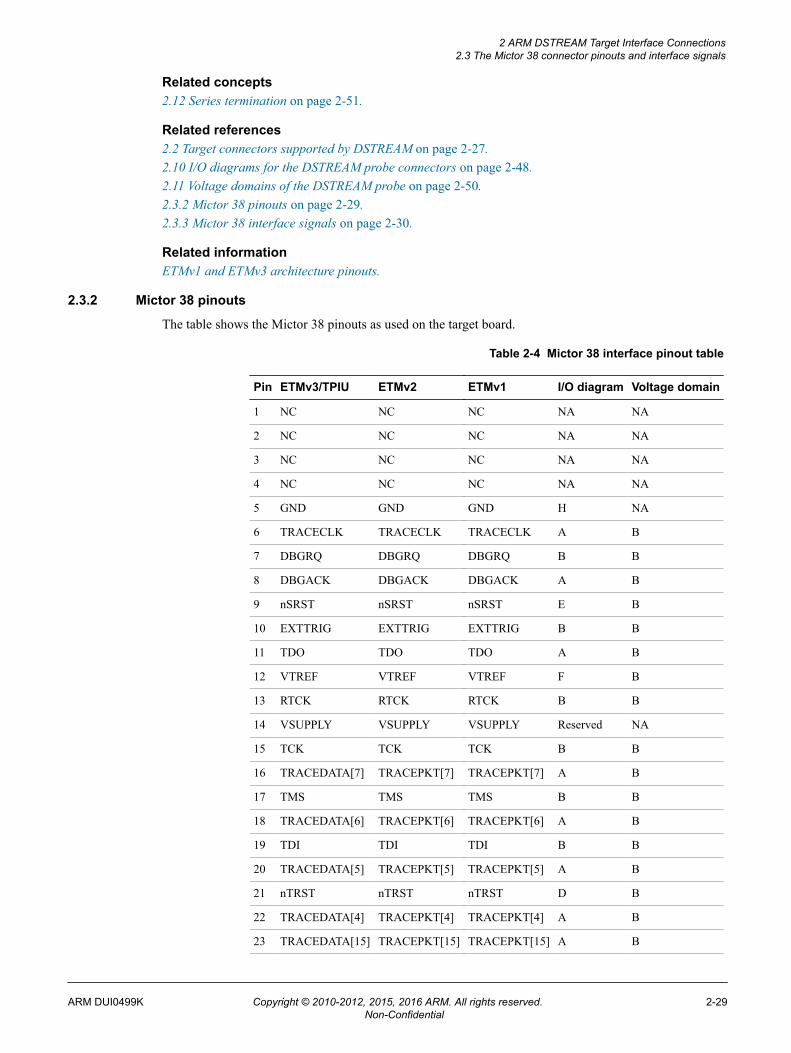
2.3.2 Mictor 38 pinouts
The table shows the Mictor 38 pinouts as used on the target board.
Table 2-4 Mictor 38 interface pinout table
Pin ETMv3/TPIU ETMv2 ETMv1 I/O diagram Voltage domain
1 NC NC NC NA NA
2 NC NC NC NA NA
3 NC NC NC NA NA
4 NC NC NC NA NA
5 GND GND GND H NA
6 TRACECLK TRACECLK TRACECLK A B
7 DBGRQ DBGRQ DBGRQ B B
8 DBGACK DBGACK DBGACK A B
9 nSRST nSRST nSRST E B
10 EXTTRIG EXTTRIG EXTTRIG B B
11 TDO TDO TDO A B
12 VTREF VTREF VTREF F B
13 RTCK RTCK RTCK B B
14 VSUPPLY VSUPPLY VSUPPLY Reserved NA
15 TCK TCK TCK B B
16 TRACEDATA[7] TRACEPKT[7] TRACEPKT[7] A B
17 TMS TMS TMS B B
18 TRACEDATA[6] TRACEPKT[6] TRACEPKT[6] A B
19 TDI TDI TDI B B
20 TRACEDATA[5] TRACEPKT[5] TRACEPKT[5] A B
21 nTRST nTRST nTRST D B
22 TRACEDATA[4] TRACEPKT[4] TRACEPKT[4] A B
23 TRACEDATA[15] TRACEPKT[15] TRACEPKT[15] A B
2 ARM DSTREAM Target Interface Connections2.3 The Mictor 38 connector pinouts and interface signals
ARM DUI0499K Copyright © 2010-2012, 2015, 2016 ARM. All rights reserved. 2-29Non-Confidential

Table 2-4 Mictor 38 interface pinout table (continued)
Pin ETMv3/TPIU ETMv2 ETMv1 I/O diagram Voltage domain
24 TRACEDATA[3] TRACEPKT[3] TRACEPKT[3] A B
25 TRACEDATA[14] TRACEPKT[14] TRACEPKT[14] A B
26 TRACEDATA[2] TRACEPKT[2] TRACEPKT[2] A B
27 TRACEDATA[13] TRACEPKT[13] TRACEPKT[13] A B
28 TRACEDATA[1] TRACEPKT[1] TRACEPKT[1] A B
29 TRACEDATA[12] TRACEPKT[12] TRACEPKT[12] A B
30 Logic 0 TRACEPKT[0] TRACEPKT[0] A B
31 TRACEDATA[11] TRACEPKT[11] TRACEPKT[11] A B
32 Logic 0 PIPESTAT[3] TRACESYNC A B
33 TRACEDATA[10] TRACEPKT[10] A B
34 Logic 1 PIPESTAT[2] PIPESTAT[2] A B
35 TRACEDATA[9] TRACEPKT[9] TRACEPKT[9] A B
36 TRACECTL PIPESTAT[1] PIPESTAT[1] A B
37 TRACEDATA[8] TRACEPKT[8] TRACEPKT[8] A B
38 TRACEDATA[0] PIPESTAT[0] PIPESTAT[0] A B
2.3.3 Mictor 38 interface signals
The table describes the signals on the Mictor 38 interface.
Table 2-5 Mictor 38 signals
Signal I/O Description
TRACEPKT,TRACEDATA,PIPESTAT,TRACESYNC,TRACECTL
Input These pins provide DSTREAM with ETM/TPIU trace data in the various formats shown above.You are advised to series terminate these signals close to the target processor.
TRACECLK Input The Trace Clock pin provides DSTREAM with the clock signal necessary to sample all of the tracedata signals above. You are advised to series terminate TRACECLK close to the target processor.
TDI Output The Test Data In pin provides serial data to the target during debugging. TDI can be pulled HIGHon the target.
TDO Input The Test Data Out pin receives serial data from the target during debugging. You are advised toseries terminate TDO close to the target processor. TDO is typically pulled HIGH on the target.
TMS Output The Test Mode Select pin sets the state of the Test Access Port (TAP) controller on the target. TMScan be pulled HIGH on the target to keep the TAP controller inactive when not in use.
TCK Output The Test Clock pin clocks data into the TDI and TMS inputs of the target. TCK is typically pulledHIGH on the target.
RTCK Input The Return Test Clock pin echos the test clock signal back to DSTREAM for use with adaptivemode clocking. If RTCK is generated by the target processor, you are advised to series terminateit. RTCK can be pulled HIGH or LOW on the target when not in use.
2 ARM DSTREAM Target Interface Connections2.3 The Mictor 38 connector pinouts and interface signals
ARM DUI0499K Copyright © 2010-2012, 2015, 2016 ARM. All rights reserved. 2-30Non-Confidential

Table 2-5 Mictor 38 signals (continued)
Signal I/O Description
nTRST Output The Test Reset pin resets the TAP controller of the processor to allow debugging to take place.nTRST is typically pulled HIGH on the target and pulled strong-LOW by DSTREAM to initiate areset. The polarity and strength of nTRST is configurable.
nSRST Input/Output
The System Reset pin fully resets the target. This signal can be initiated by DSTREAM or by thetarget board (which is then detected by DSTREAM). nSRST is typically pulled HIGH on thetarget and pulled strong-LOW to initiate a reset. The polarity and strength of nSRST isconfigurable.
DBGRQ Output The Debug Request pin stops the target processor and puts it into debug state. DBGRQ is rarelyused by current systems and is usually pulled LOW on the target.
DBGACK Input The Debug Acknowledge pin notifies DSTREAM that a debug request has been received and thetarget processor is now in debug state. DBGACK is rarely used by current systems and is usuallypulled LOW on the target.
VTREF Input The Voltage Target Reference pin supplies DSTREAM with the debug rail voltage of the target tomatch its I/O logic levels. VTREF can be tied HIGH on the target. If VTREF is pulled HIGH by aresistor, its value must be no greater than 100Ω.
VSUPPLY - The Voltage Supply pin is not used by DSTREAM and must be left unconnected.
GND - Ground.
2 ARM DSTREAM Target Interface Connections2.3 The Mictor 38 connector pinouts and interface signals
ARM DUI0499K Copyright © 2010-2012, 2015, 2016 ARM. All rights reserved. 2-31Non-Confidential
2.4 The ARM JTAG 20 connector pinouts and interface signalsThis describes the ARM JTAG 20 connector.
This section contains the following subsections:• 2.4.1 About the ARM JTAG 20 connector on page 2-32.• 2.4.2 ARM JTAG 20 pinouts on page 2-32.• 2.4.3 ARM JTAG 20 interface signals on page 2-33.
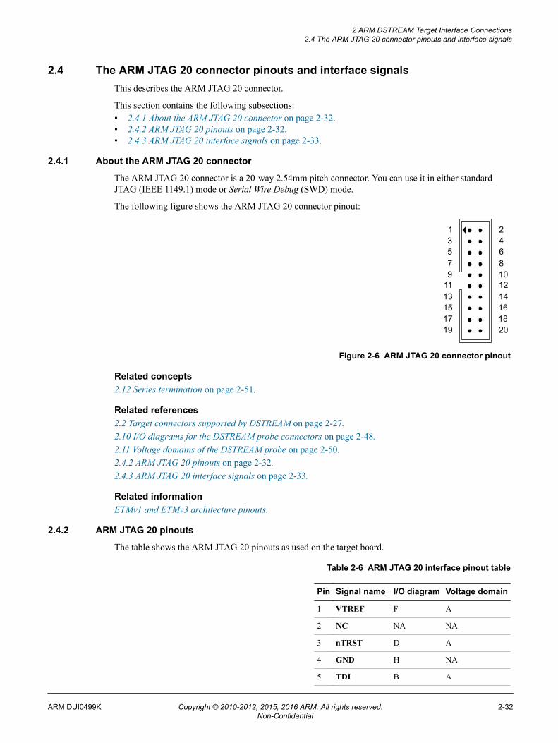
2.4.1 About the ARM JTAG 20 connector
The ARM JTAG 20 connector is a 20-way 2.54mm pitch connector. You can use it in either standardJTAG (IEEE 1149.1) mode or Serial Wire Debug (SWD) mode.
The following figure shows the ARM JTAG 20 connector pinout:
24681012
161820
14
13579
11
151719
13
Figure 2-6 ARM JTAG 20 connector pinout
Related concepts2.12 Series termination on page 2-51.
Related references2.2 Target connectors supported by DSTREAM on page 2-27.2.10 I/O diagrams for the DSTREAM probe connectors on page 2-48.2.11 Voltage domains of the DSTREAM probe on page 2-50.2.4.2 ARM JTAG 20 pinouts on page 2-32.2.4.3 ARM JTAG 20 interface signals on page 2-33.
Related informationETMv1 and ETMv3 architecture pinouts.
2.4.2 ARM JTAG 20 pinouts
The table shows the ARM JTAG 20 pinouts as used on the target board.
Table 2-6 ARM JTAG 20 interface pinout table
Pin Signal name I/O diagram Voltage domain
1 VTREF F A
2 NC NA NA
3 nTRST D A
4 GND H NA
5 TDI B A
2 ARM DSTREAM Target Interface Connections2.4 The ARM JTAG 20 connector pinouts and interface signals
ARM DUI0499K Copyright © 2010-2012, 2015, 2016 ARM. All rights reserved. 2-32Non-Confidential
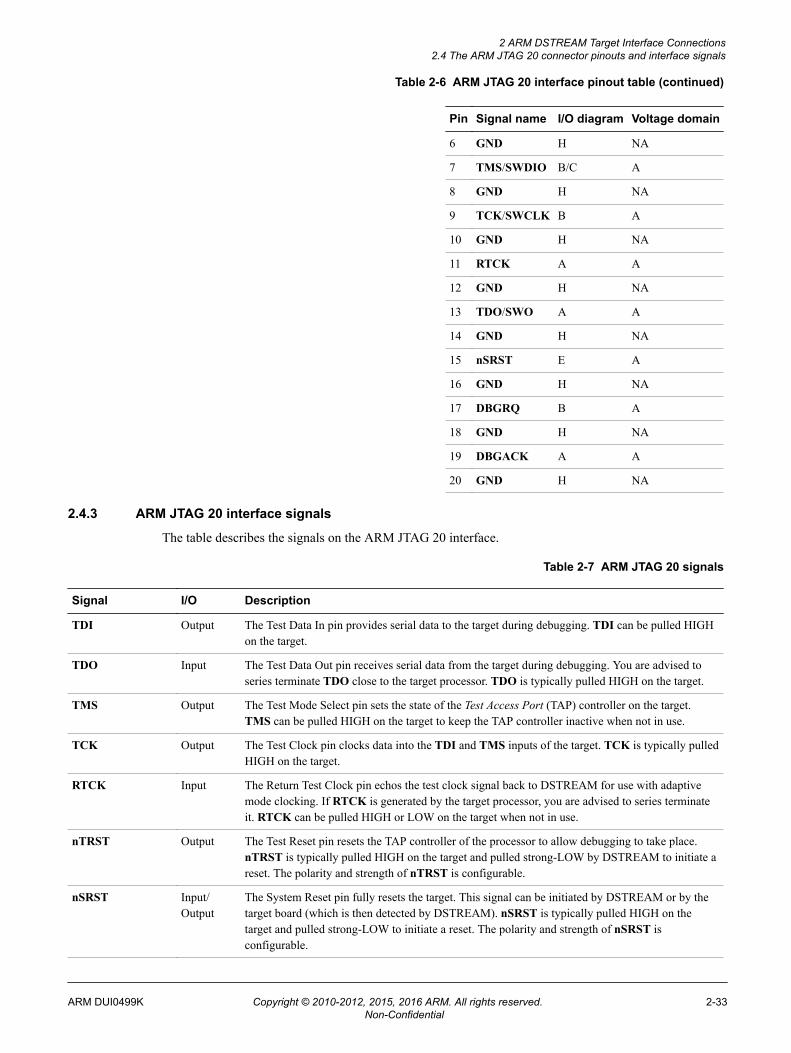
Table 2-6 ARM JTAG 20 interface pinout table (continued)
Pin Signal name I/O diagram Voltage domain
6 GND H NA
7 TMS/SWDIO B/C A
8 GND H NA
9 TCK/SWCLK B A
10 GND H NA
11 RTCK A A
12 GND H NA
13 TDO/SWO A A
14 GND H NA
15 nSRST E A
16 GND H NA
17 DBGRQ B A
18 GND H NA
19 DBGACK A A
20 GND H NA
2.4.3 ARM JTAG 20 interface signals
The table describes the signals on the ARM JTAG 20 interface.
Table 2-7 ARM JTAG 20 signals
Signal I/O Description
TDI Output The Test Data In pin provides serial data to the target during debugging. TDI can be pulled HIGHon the target.
TDO Input The Test Data Out pin receives serial data from the target during debugging. You are advised toseries terminate TDO close to the target processor. TDO is typically pulled HIGH on the target.
TMS Output The Test Mode Select pin sets the state of the Test Access Port (TAP) controller on the target.TMS can be pulled HIGH on the target to keep the TAP controller inactive when not in use.
TCK Output The Test Clock pin clocks data into the TDI and TMS inputs of the target. TCK is typically pulledHIGH on the target.
RTCK Input The Return Test Clock pin echos the test clock signal back to DSTREAM for use with adaptivemode clocking. If RTCK is generated by the target processor, you are advised to series terminateit. RTCK can be pulled HIGH or LOW on the target when not in use.
nTRST Output The Test Reset pin resets the TAP controller of the processor to allow debugging to take place.nTRST is typically pulled HIGH on the target and pulled strong-LOW by DSTREAM to initiate areset. The polarity and strength of nTRST is configurable.
nSRST Input/Output
The System Reset pin fully resets the target. This signal can be initiated by DSTREAM or by thetarget board (which is then detected by DSTREAM). nSRST is typically pulled HIGH on thetarget and pulled strong-LOW to initiate a reset. The polarity and strength of nSRST isconfigurable.
2 ARM DSTREAM Target Interface Connections2.4 The ARM JTAG 20 connector pinouts and interface signals
ARM DUI0499K Copyright © 2010-2012, 2015, 2016 ARM. All rights reserved. 2-33Non-Confidential

Table 2-7 ARM JTAG 20 signals (continued)
Signal I/O Description
DBGRQ Output The Debug Request pin stops the target processor and puts it into debug state. DBGRQ is rarelyused by current systems and is usually pulled LOW on the target.
DBGACK Input The Debug Acknowledge pin notifies DSTREAM that a debug request has been received and thetarget processor is now in debug state. DBGACK is rarely used by current systems and is usuallypulled LOW on the target.
SWDIO (SWDmode)
Input/Output
The Serial Wire Data I/O pin sends and receives serial data to and from the target duringdebugging. You are advised to series terminate SWDIO close to the target processor.
SWCLK(SWDmode)
Output The Serial Wire Clock pin clocks data into and out of the target during debugging.
SWO (SWD mode) Input The Serial Wire Output pin provides trace data to DSTREAM. You are advised to series terminateSWO close to the target processor.
VTREF Input The Voltage Target Reference pin supplies DSTREAM with the debug rail voltage of the target tomatch its I/O logic levels. VTREF can be tied HIGH on the target. If VTREF is pulled HIGH by aresistor, its value must be no greater than 100Ω.
GND - Ground.
2 ARM DSTREAM Target Interface Connections2.4 The ARM JTAG 20 connector pinouts and interface signals
ARM DUI0499K Copyright © 2010-2012, 2015, 2016 ARM. All rights reserved. 2-34Non-Confidential
2.5 The TI JTAG 14 connector pinouts and interface signalsThis describes the TI JTAG 14 connector.
This section contains the following subsections:• 2.5.1 About the TI JTAG 14 connector on page 2-35.• 2.5.2 TI JTAG 14 pinouts on page 2-35.• 2.5.3 TI JTAG 14 interface signals on page 2-36.
2.5.1 About the TI JTAG 14 connector
You can use the TI JTAG 14 connector in either standard JTAG (IEEE 1149.1) mode or Serial WireDebug (SWD) mode.
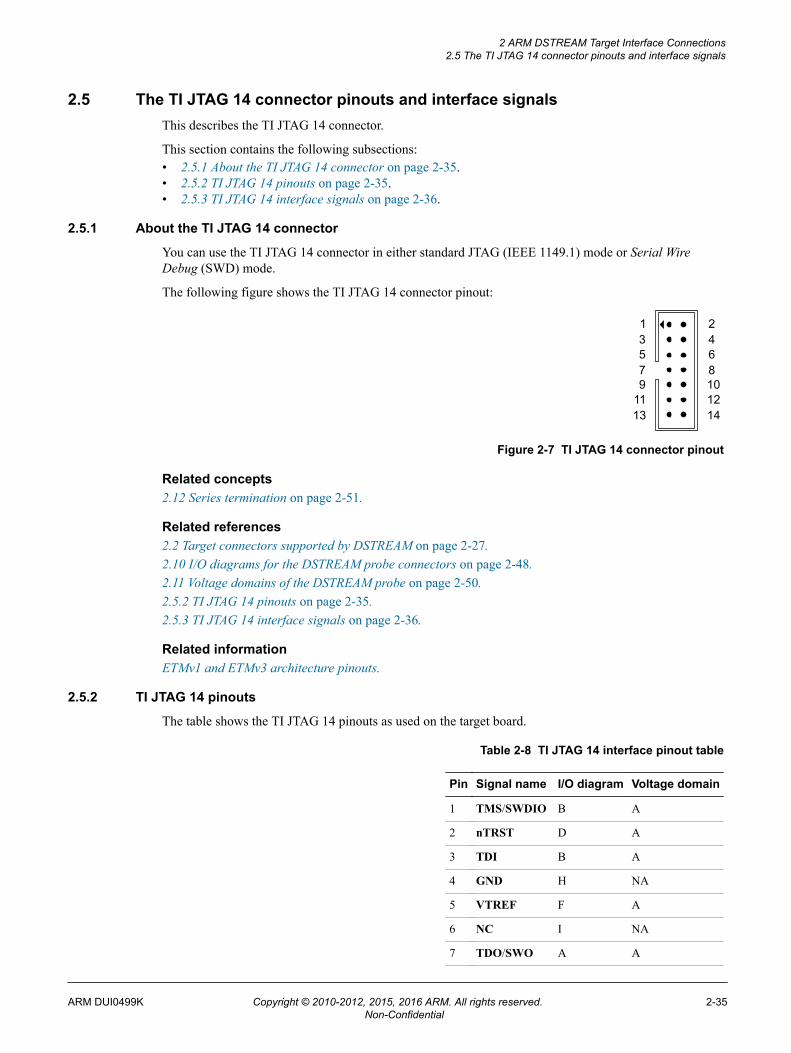
The following figure shows the TI JTAG 14 connector pinout:
13579
1113
2468101214
Figure 2-7 TI JTAG 14 connector pinout
Related concepts2.12 Series termination on page 2-51.
Related references2.2 Target connectors supported by DSTREAM on page 2-27.2.10 I/O diagrams for the DSTREAM probe connectors on page 2-48.2.11 Voltage domains of the DSTREAM probe on page 2-50.2.5.2 TI JTAG 14 pinouts on page 2-35.2.5.3 TI JTAG 14 interface signals on page 2-36.
Related informationETMv1 and ETMv3 architecture pinouts.
2.5.2 TI JTAG 14 pinouts
The table shows the TI JTAG 14 pinouts as used on the target board.
Table 2-8 TI JTAG 14 interface pinout table
Pin Signal name I/O diagram Voltage domain
1 TMS/SWDIO B A
2 nTRST D A
3 TDI B A
4 GND H NA
5 VTREF F A
6 NC I NA
7 TDO/SWO A A
2 ARM DSTREAM Target Interface Connections2.5 The TI JTAG 14 connector pinouts and interface signals
ARM DUI0499K Copyright © 2010-2012, 2015, 2016 ARM. All rights reserved. 2-35Non-Confidential
Table 2-8 TI JTAG 14 interface pinout table (continued)
Pin Signal name I/O diagram Voltage domain
8 GND H NA
9 RTCK A A
10 GND H NA
11 TCK/SWCLK B A
12 GND H NA
13 EMU0 B A
14 EMU1 A A
2.5.3 TI JTAG 14 interface signals
The table describes the signals on the TI JTAG 14 interface.
Table 2-9 TI JTAG 14 signals
Signal I/O Description
TDI Output The Test Data In pin provides serial data to the target during debugging. TDI can be pulled HIGHon the target.
TDO Input The Test Data Out pin receives serial data from the target during debugging. You are advised toseries terminate TDO close to the target processor. TDO is typically pulled HIGH on the target.
TMS Output The Test Mode Select pin sets the state of the Test Access Port (TAP) controller on the target.TMS can be pulled HIGH on the target to keep the TAP controller inactive when not in use.
TCK Output The Test Clock pin clocks data into the TDI and TMS inputs of the target. TCK is typicallypulled HIGH on the target.
RTCK Input The Return Test Clock pin echos the test clock signal back to DSTREAM for use with adaptivemode clocking. If RTCK is generated by the target processor, you are advised to series terminateit. RTCK can be pulled HIGH or LOW on the target when not in use.
nTRST Output The Test Reset pin resets the TAP controller of the processor to allow debugging to take place.nTRST is typically pulled HIGH on the target and pulled strong-LOW by DSTREAM to initiate areset. The polarity and strength of nTRST is configurable.
EMU0 - The EMU0 pin is a general I/O pin but is not currently supported by DSTREAM. EMU0 can bepulled high, low or be left open-circuit on the target.
EMU1 - The EMU1 pin is a general I/O pin but is not currently supported by DSTREAM. EMU0 can bepulled high, low or be left open-circuit on the target.
SWDIO (SWDmode)
Input/Output
The Serial Wire Data I/O pin sends and receives serial data to and from the target duringdebugging. You are advised to series terminate SWDIO close to the target processor.
SWCLK(SWDmode)
Output The Serial Wire Clock pin clocks data into and out of the target during debugging.
SWO (SWD mode) Input The Serial Wire Output pin provides trace data to DSTREAM. You are advised to series terminateSWO close to the target processor.
VTREF Input The Voltage Target Reference pin supplies DSTREAM with the debug rail voltage of the target tomatch its I/O logic levels. VTREF can be tied HIGH on the target. If VTREF is pulled HIGH bya resistor, its value must be no greater than 100Ω.
GND - Ground.
2 ARM DSTREAM Target Interface Connections2.5 The TI JTAG 14 connector pinouts and interface signals
ARM DUI0499K Copyright © 2010-2012, 2015, 2016 ARM. All rights reserved. 2-36Non-Confidential

2.6 The ARM JTAG 14 connector pinouts and interface signalsThis describes the ARM JTAG 14 connector.
This section contains the following subsections:• 2.6.1 About the ARM JTAG 14 connector on page 2-37.• 2.6.2 ARM JTAG 14 pinouts on page 2-37.• 2.6.3 ARM JTAG 14 interface signals on page 2-38.
2.6.1 About the ARM JTAG 14 connector
You can use the ARM JTAG 14 connector in either standard JTAG (IEEE 1149.1) mode or Serial WireDebug (SWD) mode.
The following figure shows the ARM JTAG 14 connector pinout:
13579
1113
2468101214
Figure 2-8 ARM JTAG 14 connector pinout
Related concepts2.12 Series termination on page 2-51.
Related references2.2 Target connectors supported by DSTREAM on page 2-27.2.10 I/O diagrams for the DSTREAM probe connectors on page 2-48.2.11 Voltage domains of the DSTREAM probe on page 2-50.2.6.2 ARM JTAG 14 pinouts on page 2-37.2.6.3 ARM JTAG 14 interface signals on page 2-38.
Related informationETMv1 and ETMv3 architecture pinouts.
2.6.2 ARM JTAG 14 pinouts
The table shows the ARM JTAG 14 pinouts as used on the target board.
Table 2-10 ARM JTAG 14 interface pinout table
Pin Signal name I/O diagram Voltage domain
1 NC NA NA
2 GND H NA
3 nTRST D A
4 GND H NA
5 TDI B A
6 GND H NA
7 TMS/SWDIO B A
2 ARM DSTREAM Target Interface Connections2.6 The ARM JTAG 14 connector pinouts and interface signals
ARM DUI0499K Copyright © 2010-2012, 2015, 2016 ARM. All rights reserved. 2-37Non-Confidential
Table 2-10 ARM JTAG 14 interface pinout table (continued)
Pin Signal name I/O diagram Voltage domain
8 GND H NA
9 TCK/SWCLK B A
10 GND H NA
11 TDO/SWO A A
12 nSRST E A
13 VTREF F A
14 GND H NA
2.6.3 ARM JTAG 14 interface signals
The table describes the signals on the ARM JTAG 14 interface.
Table 2-11 ARM JTAG 14 signals
Signal I/O Description
TDI Output The Test Data In pin provides serial data to the target during debugging. TDI can be pulled HIGHon the target.
TDO Input The Test Data Out pin receives serial data from the target during debugging. You are advised toseries terminate TDO close to the target processor. TDO is typically pulled HIGH on the target.
TMS Output The Test Mode Select pin sets the state of the Test Access Port (TAP) controller on the target.TMS can be pulled HIGH on the target to keep the TAP controller inactive when not in use.
TCK Output The Test Clock pin clocks data into the TDI and TMS inputs of the target. TCK is typicallypulled HIGH on the target.
nTRST Output The Test Reset pin resets the TAP controller of the processor to allow debugging to take place.nTRST is typically pulled HIGH on the target and pulled strong-LOW by DSTREAM to initiatea reset. The polarity and strength of nTRST is configurable.
nSRST Input/Output
The System Reset pin fully resets the target. This signal can be initiated by DSTREAM or by thetarget board (which is then detected by DSTREAM). nSRST is typically pulled HIGH on thetarget and pulled strong-LOW to initiate a reset. The polarity and strength of nSRST isconfigurable.
SWDIO (SWDmode)
Input/Output
The Serial Wire Data I/O pin sends and receives serial data to and from the target duringdebugging. You are advised to series terminate SWDIO close to the target processor.
SWCLK(SWDmode)
Output The Serial Wire Clock pin clocks data into and out of the target during debugging.
SWO (SWD mode) Input The Serial Wire Output pin provides trace data to DSTREAM. You are advised to seriesterminate SWO close to the target processor.
VTREF Input The Voltage Target Reference pin supplies DSTREAM with the debug rail voltage of the target tomatch its I/O logic levels. VTREF can be tied HIGH on the target. If VTREF is pulled HIGH bya resistor, its value must be no greater than 100Ω.
GND - Ground.
2 ARM DSTREAM Target Interface Connections2.6 The ARM JTAG 14 connector pinouts and interface signals
ARM DUI0499K Copyright © 2010-2012, 2015, 2016 ARM. All rights reserved. 2-38Non-Confidential
2.7 The CoreSight 10 connector pinouts and interface signalsThis describes the CoreSight 10 connector.
This section contains the following subsections:• 2.7.1 About the CoreSight 10 connector on page 2-39.• 2.7.2 CoreSight 10 pinouts on page 2-39.• 2.7.3 CoreSight 10 interface signals on page 2-40.
2.7.1 About the CoreSight 10 connector
You can use the CoreSight 10 connector in either standard JTAG (IEEE 1149.1) mode or Serial WireDebug (SWD) mode.
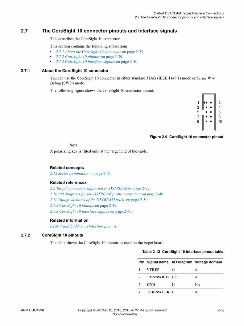
The following figure shows the CoreSight 10 connector pinout:
246810
13579
Figure 2-9 CoreSight 10 connector pinout
Note
A polarizing key is fitted only at the target end of the cable.
Related concepts2.12 Series termination on page 2-51.
Related references2.2 Target connectors supported by DSTREAM on page 2-27.2.10 I/O diagrams for the DSTREAM probe connectors on page 2-48.2.11 Voltage domains of the DSTREAM probe on page 2-50.2.7.2 CoreSight 10 pinouts on page 2-39.2.7.3 CoreSight 10 interface signals on page 2-40.
Related informationETMv1 and ETMv3 architecture pinouts.
2.7.2 CoreSight 10 pinouts
The table shows the CoreSight 10 pinouts as used on the target board.
Table 2-12 CoreSight 10 interface pinout table
Pin Signal name I/O diagram Voltage domain
1 VTREF G A
2 TMS/SWDIO B/C A
3 GND H NA
4 TCK/SWCLK B A
2 ARM DSTREAM Target Interface Connections2.7 The CoreSight 10 connector pinouts and interface signals
ARM DUI0499K Copyright © 2010-2012, 2015, 2016 ARM. All rights reserved. 2-39Non-Confidential

Table 2-12 CoreSight 10 interface pinout table (continued)
Pin Signal name I/O diagram Voltage domain
5 GND H NA
6 TDO/SWO A A
7 KEY (NC) NA NA
8 TDI B A
9 GND H NA
10 nSRST E A
2.7.3 CoreSight 10 interface signals
The table describes the signals on the CoreSight 10 interface.
Table 2-13 CoreSight 10 signals
Signal I/O Description
TDI Output The Test Data In pin provides serial data to the target during debugging. TDI can be pulledHIGH on the target.
TDO Input The Test Data Out pin receives serial data from the target during debugging. You are advised toseries terminate TDO close to the target processor. TDO is typically pulled HIGH on the target.
TMS Output The Test Mode Select pin sets the state of the Test Access Port (TAP) controller on the target.TMS can be pulled HIGH on the target to keep the TAP controller inactive when not in use.
TCK Output The Test Clock pin clocks data into the TDI and TMS inputs of the target. TCK is typicallypulled HIGH on the target.
nSRST Input/Output
The System Reset pin fully resets the target. This signal can be initiated by DSTREAM or by thetarget board (which is then detected by DSTREAM). nSRST is typically pulled HIGH on thetarget and pulled strong-LOW to initiate a reset. The polarity and strength of nSRST isconfigurable.
SWDIO (SWDmode)
Input/Output
The Serial Wire Data I/O pin sends and receives serial data to and from the target duringdebugging. You are advised to series terminate SWDIO close to the target processor.
SWCLK(SWDmode)
Output The Serial Wire Clock pin clocks data into and out of the target during debugging.
SWO (SWD mode) Input The Serial Wire Output pin provides trace data to DSTREAM. You are advised to seriesterminate SWO close to the target processor.
VTREF Input The Voltage Target Reference pin supplies DSTREAM with the debug rail voltage of the targetto match its I/O logic levels. VTREF can be tied HIGH on the target. If VTREF is pulled HIGHby a resistor, its value must be no greater than 100Ω.
GND - Ground.
KEY - This pin must not be present on the target connector.
2 ARM DSTREAM Target Interface Connections2.7 The CoreSight 10 connector pinouts and interface signals
ARM DUI0499K Copyright © 2010-2012, 2015, 2016 ARM. All rights reserved. 2-40Non-Confidential

2.8 The CoreSight 20 connector pinouts and interface signalsThis describes the CoreSight 20 connector.
This section contains the following subsections:• 2.8.1 About the CoreSight 20 connector on page 2-41.• 2.8.2 CoreSight 20 pinouts on page 2-41.• 2.8.3 CoreSight 20 interface signals on page 2-42.
2.8.1 About the CoreSight 20 connector
You can use the CoreSight 20 connector in either standard JTAG (IEEE 1149.1) mode or Serial WireDebug (SWD) mode. It can also optionally capture up to 4 bits of parallel trace in Trace Port InterfaceUnit (TPIU) continuous mode.
When this connector is configured to be a parallel trace source, pins 12 to 20 switch to their alternatetrace functions.
The following figure shows the CoreSight 20 connector pinout:
24681012
161820
14
13579
11
151719
13
Figure 2-10 CoreSight 20 connector pinout
Note
A polarizing key is fitted only at the target end of the cable.
Related concepts2.12 Series termination on page 2-51.
Related references2.2 Target connectors supported by DSTREAM on page 2-27.2.10 I/O diagrams for the DSTREAM probe connectors on page 2-48.2.11 Voltage domains of the DSTREAM probe on page 2-50.2.8.2 CoreSight 20 pinouts on page 2-41.2.8.3 CoreSight 20 interface signals on page 2-42.
Related informationETMv1 and ETMv3 architecture pinouts.
2.8.2 CoreSight 20 pinouts
The table shows the CoreSight 20 pinouts as used on the target board.
2 ARM DSTREAM Target Interface Connections2.8 The CoreSight 20 connector pinouts and interface signals
ARM DUI0499K Copyright © 2010-2012, 2015, 2016 ARM. All rights reserved. 2-41Non-Confidential
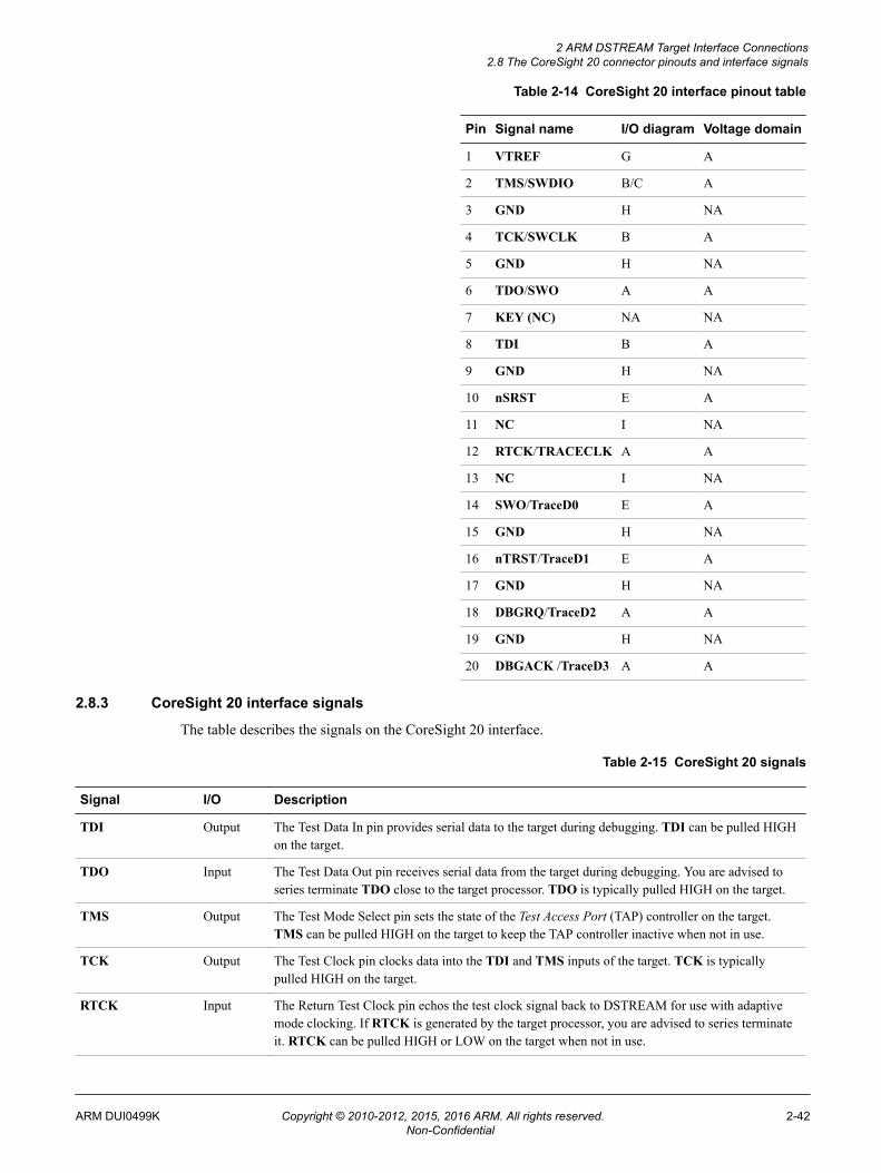
Table 2-14 CoreSight 20 interface pinout table
Pin Signal name I/O diagram Voltage domain
1 VTREF G A
2 TMS/SWDIO B/C A
3 GND H NA
4 TCK/SWCLK B A
5 GND H NA
6 TDO/SWO A A
7 KEY (NC) NA NA
8 TDI B A
9 GND H NA
10 nSRST E A
11 NC I NA
12 RTCK/TRACECLK A A
13 NC I NA
14 SWO/TraceD0 E A
15 GND H NA
16 nTRST/TraceD1 E A
17 GND H NA
18 DBGRQ/TraceD2 A A
19 GND H NA
20 DBGACK /TraceD3 A A
2.8.3 CoreSight 20 interface signals
The table describes the signals on the CoreSight 20 interface.
Table 2-15 CoreSight 20 signals
Signal I/O Description
TDI Output The Test Data In pin provides serial data to the target during debugging. TDI can be pulled HIGHon the target.
TDO Input The Test Data Out pin receives serial data from the target during debugging. You are advised toseries terminate TDO close to the target processor. TDO is typically pulled HIGH on the target.
TMS Output The Test Mode Select pin sets the state of the Test Access Port (TAP) controller on the target.TMS can be pulled HIGH on the target to keep the TAP controller inactive when not in use.
TCK Output The Test Clock pin clocks data into the TDI and TMS inputs of the target. TCK is typicallypulled HIGH on the target.
RTCK Input The Return Test Clock pin echos the test clock signal back to DSTREAM for use with adaptivemode clocking. If RTCK is generated by the target processor, you are advised to series terminateit. RTCK can be pulled HIGH or LOW on the target when not in use.
2 ARM DSTREAM Target Interface Connections2.8 The CoreSight 20 connector pinouts and interface signals
ARM DUI0499K Copyright © 2010-2012, 2015, 2016 ARM. All rights reserved. 2-42Non-Confidential
Table 2-15 CoreSight 20 signals (continued)
Signal I/O Description
nTRST Output The Test Reset pin resets the TAP controller of the processor to allow debugging to take place.nTRST is typically pulled HIGH on the target and pulled strong-LOW by DSTREAM to initiate areset. The polarity and strength of nTRST is configurable.
nSRST Input/Output
The System Reset pin fully resets the target. This signal can be initiated by DSTREAM or by thetarget board (which is then detected by DSTREAM). nSRST is typically pulled HIGH on thetarget and pulled strong-LOW to initiate a reset. The polarity and strength of nSRST isconfigurable.
DBGRQ Output The Debug Request pin stops the target processor and puts it into debug state. DBGRQ is rarelyused by current systems and is usually pulled LOW on the target.
DBGACK Input The Debug Acknowledge pin notifies DSTREAM that a debug request has been received and thetarget processor is now in debug state. DBGACK is rarely used by current systems and is usuallypulled LOW on the target.
SWDIO (SWDmode)
Input/Output
The Serial Wire Data I/O pin sends and receives serial data to and from the target duringdebugging. You are advised to series terminate SWDIO close to the target processor.
SWCLK(SWDmode)
Output The Serial Wire Clock pin clocks data into and out of the target during debugging.
SWO (SWD mode) Input The Serial Wire Output pin provides trace data to DSTREAM. You are advised to series terminateSWO close to the target processor. SWO is configurable to be captured on pin 6 or 14.
TraceD[0-3] Input The Trace Data [0-3] pins provide DSTREAM with TPIU continuous mode trace data from thetarget. You are advised to series terminate these signals close to the target processor.
TRACECLK (Tracemode)
Input The Trace Clock pin provides DSTREAM with the clock signal necessary to sample the trace datasignals. You are advised to series terminate TRACECLK close to the target processor.
VTREF Input The Voltage Target Reference pin supplies DSTREAM with the debug rail voltage of the target tomatch its I/O logic levels. VTREF can be tied HIGH on the target. If VTREF is pulled HIGH bya resistor, its value must be no greater than 100Ω.
GND - Ground.
KEY - This pin must not be present on the target connector.
2 ARM DSTREAM Target Interface Connections2.8 The CoreSight 20 connector pinouts and interface signals
ARM DUI0499K Copyright © 2010-2012, 2015, 2016 ARM. All rights reserved. 2-43Non-Confidential
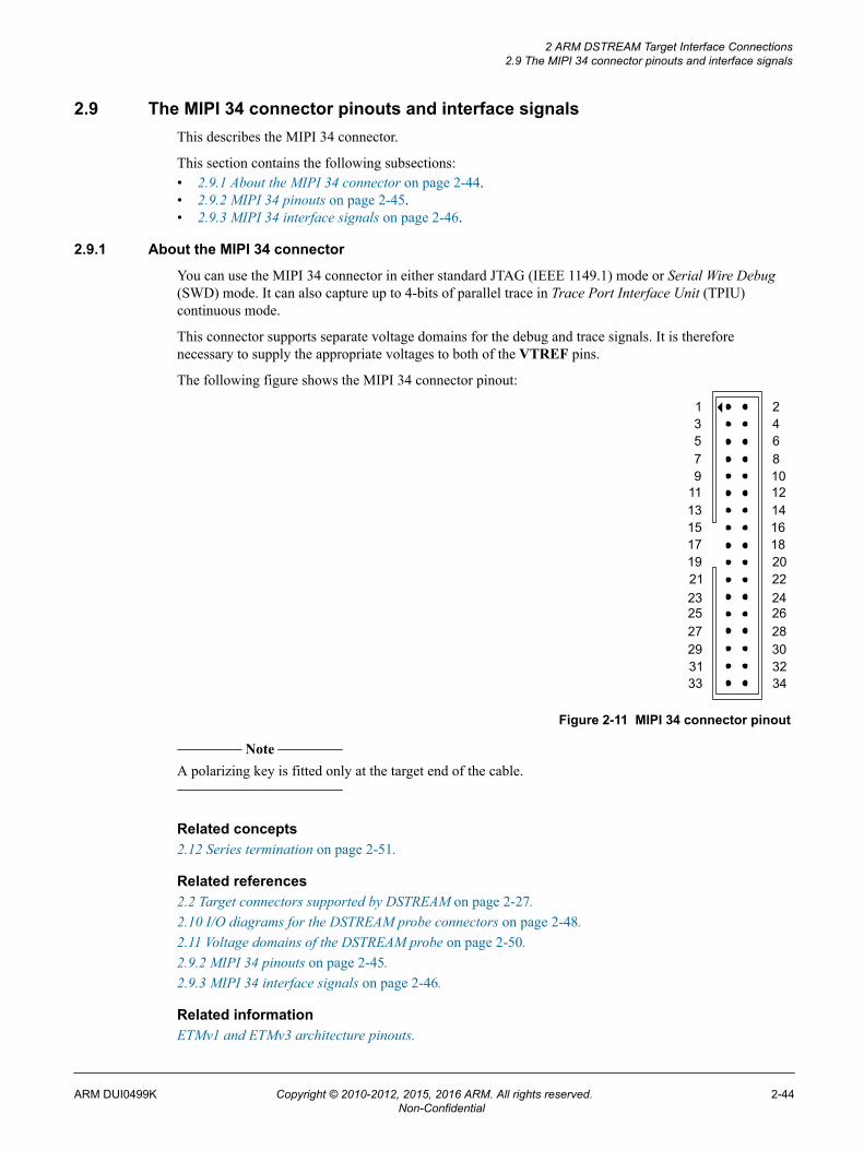
2.9 The MIPI 34 connector pinouts and interface signalsThis describes the MIPI 34 connector.
This section contains the following subsections:• 2.9.1 About the MIPI 34 connector on page 2-44.• 2.9.2 MIPI 34 pinouts on page 2-45.• 2.9.3 MIPI 34 interface signals on page 2-46.
2.9.1 About the MIPI 34 connector
You can use the MIPI 34 connector in either standard JTAG (IEEE 1149.1) mode or Serial Wire Debug(SWD) mode. It can also capture up to 4-bits of parallel trace in Trace Port Interface Unit (TPIU)continuous mode.
This connector supports separate voltage domains for the debug and trace signals. It is thereforenecessary to supply the appropriate voltages to both of the VTREF pins.
The following figure shows the MIPI 34 connector pinout:
24681012
161820
14
13579
11
151719
13
22242628303234
21232527293133
Figure 2-11 MIPI 34 connector pinout
Note
A polarizing key is fitted only at the target end of the cable.
Related concepts2.12 Series termination on page 2-51.
Related references2.2 Target connectors supported by DSTREAM on page 2-27.2.10 I/O diagrams for the DSTREAM probe connectors on page 2-48.2.11 Voltage domains of the DSTREAM probe on page 2-50.2.9.2 MIPI 34 pinouts on page 2-45.2.9.3 MIPI 34 interface signals on page 2-46.
Related informationETMv1 and ETMv3 architecture pinouts.
2 ARM DSTREAM Target Interface Connections2.9 The MIPI 34 connector pinouts and interface signals
ARM DUI0499K Copyright © 2010-2012, 2015, 2016 ARM. All rights reserved. 2-44Non-Confidential
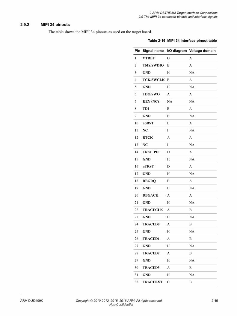
2.9.2 MIPI 34 pinouts
The table shows the MIPI 34 pinouts as used on the target board.
Table 2-16 MIPI 34 interface pinout table
Pin Signal name I/O diagram Voltage domain
1 VTREF G A
2 TMS/SWDIO B A
3 GND H NA
4 TCK/SWCLK B A
5 GND H NA
6 TDO/SWO A A
7 KEY (NC) NA NA
8 TDI B A
9 GND H NA
10 nSRST E A
11 NC I NA
12 RTCK A A
13 NC I NA
14 TRST_PD D A
15 GND H NA
16 nTRST D A
17 GND H NA
18 DBGRQ B A
19 GND H NA
20 DBGACK A A
21 GND H NA
22 TRACECLK A B
23 GND H NA
24 TRACED0 A B
25 GND H NA
26 TRACED1 A B
27 GND H NA
28 TRACED2 A B
29 GND H NA
30 TRACED3 A B
31 GND H NA
32 TRACEEXT C B
2 ARM DSTREAM Target Interface Connections2.9 The MIPI 34 connector pinouts and interface signals
ARM DUI0499K Copyright © 2010-2012, 2015, 2016 ARM. All rights reserved. 2-45Non-Confidential
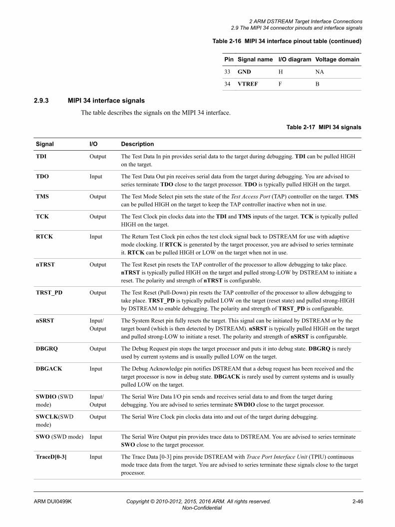
Table 2-16 MIPI 34 interface pinout table (continued)
Pin Signal name I/O diagram Voltage domain
33 GND H NA
34 VTREF F B
2.9.3 MIPI 34 interface signals
The table describes the signals on the MIPI 34 interface.
Table 2-17 MIPI 34 signals
Signal I/O Description
TDI Output The Test Data In pin provides serial data to the target during debugging. TDI can be pulled HIGHon the target.
TDO Input The Test Data Out pin receives serial data from the target during debugging. You are advised toseries terminate TDO close to the target processor. TDO is typically pulled HIGH on the target.
TMS Output The Test Mode Select pin sets the state of the Test Access Port (TAP) controller on the target. TMScan be pulled HIGH on the target to keep the TAP controller inactive when not in use.
TCK Output The Test Clock pin clocks data into the TDI and TMS inputs of the target. TCK is typically pulledHIGH on the target.
RTCK Input The Return Test Clock pin echos the test clock signal back to DSTREAM for use with adaptivemode clocking. If RTCK is generated by the target processor, you are advised to series terminateit. RTCK can be pulled HIGH or LOW on the target when not in use.
nTRST Output The Test Reset pin resets the TAP controller of the processor to allow debugging to take place.nTRST is typically pulled HIGH on the target and pulled strong-LOW by DSTREAM to initiate areset. The polarity and strength of nTRST is configurable.
TRST_PD Output The Test Reset (Pull-Down) pin resets the TAP controller of the processor to allow debugging totake place. TRST_PD is typically pulled LOW on the target (reset state) and pulled strong-HIGHby DSTREAM to enable debugging. The polarity and strength of TRST_PD is configurable.
nSRST Input/Output
The System Reset pin fully resets the target. This signal can be initiated by DSTREAM or by thetarget board (which is then detected by DSTREAM). nSRST is typically pulled HIGH on the targetand pulled strong-LOW to initiate a reset. The polarity and strength of nSRST is configurable.
DBGRQ Output The Debug Request pin stops the target processor and puts it into debug state. DBGRQ is rarelyused by current systems and is usually pulled LOW on the target.
DBGACK Input The Debug Acknowledge pin notifies DSTREAM that a debug request has been received and thetarget processor is now in debug state. DBGACK is rarely used by current systems and is usuallypulled LOW on the target.
SWDIO (SWDmode)
Input/Output
The Serial Wire Data I/O pin sends and receives serial data to and from the target duringdebugging. You are advised to series terminate SWDIO close to the target processor.
SWCLK(SWDmode)
Output The Serial Wire Clock pin clocks data into and out of the target during debugging.
SWO (SWD mode) Input The Serial Wire Output pin provides trace data to DSTREAM. You are advised to series terminateSWO close to the target processor.
TraceD[0-3] Input The Trace Data [0-3] pins provide DSTREAM with Trace Port Interface Unit (TPIU) continuousmode trace data from the target. You are advised to series terminate these signals close to the targetprocessor.
2 ARM DSTREAM Target Interface Connections2.9 The MIPI 34 connector pinouts and interface signals
ARM DUI0499K Copyright © 2010-2012, 2015, 2016 ARM. All rights reserved. 2-46Non-Confidential

Table 2-17 MIPI 34 signals (continued)
Signal I/O Description
TRACECLK Input The Trace Clock pin provides DSTREAM with the clock signal necessary to sample the trace datasignals. You are advised to series terminate TRACECLK close to the target processor.
TRACEEXT Input The Trace Extension pin is a generic trace sideband pin. TRACEEXT is not currently supportedby DSTREAM. TRACEEXT can be pulled high, low, or left unconnected on the target.
VTREF Input The Voltage Target Reference pin supplies DSTREAM with the debug rail voltage of the target tomatch its I/O logic levels. VTREF can be tied HIGH on the target. If VTREF is pulled HIGH by aresistor, its value must be no greater than 100Ω.
GND - Ground.
KEY - This pin must not be present on the target connector.
2 ARM DSTREAM Target Interface Connections2.9 The MIPI 34 connector pinouts and interface signals
ARM DUI0499K Copyright © 2010-2012, 2015, 2016 ARM. All rights reserved. 2-47Non-Confidential

2.10 I/O diagrams for the DSTREAM probe connectorsThe diagrams show the Pin I/O circuits for the debug and trace connectors on the DSTREAM probe.
Diagram A - InputThe input circuit diagram is shown in the following figure:
33R
-
- -
V REF/2
Figure 2-12 Input
Diagram B - OutputThe output circuit diagram is shown in the following figure:
33R
Figure 2-13 Output
Diagram C - Input/OutputThe input/output circuit diagram is shown in the following figure:
33R
-
- -
V REF/2
Figure 2-14 Input/Output
Diagram D - Reset outputThe reset output circuit diagram is shown in the following figure:
33R
4K7
Strong driver
Weak driver
Figure 2-15 Reset output
Diagram E - Reset output with feedbackThe reset output with feedback circuit diagram is shown in the following figure:
33R
4K7
Strong driver
Weak driver
-
- -
V REF/2
Figure 2-16 Reset output with feedback
2 ARM DSTREAM Target Interface Connections2.10 I/O diagrams for the DSTREAM probe connectors
ARM DUI0499K Copyright © 2010-2012, 2015, 2016 ARM. All rights reserved. 2-48Non-Confidential

Diagram F - VTRef inputThe VTRef input circuit diagram is shown in the following figure:
33R
-
- -
10K
~0.6VTarget detect
Buffered VTREF
- -
-
Figure 2-17 VTRef input
Diagram G - VTRef input (decoupled)The VTRef input (decoupled) circuit diagram is shown in the following figure:
33R
-
- -
~0.6VTarget detect
Buffered VTREF
- -
-
10K100nF
Figure 2-18 VTRef input (decoupled)
Diagram H - GroundThe Ground circuit diagram is shown in the following figure:
33R100nF
Figure 2-19 Ground
Diagram I - AC GroundThe AC Ground circuit diagram is shown in the following figure:
100nF
Figure 2-20 AC Ground
Related concepts2.12 Series termination on page 2-51.
Related references2.2 Target connectors supported by DSTREAM on page 2-27.2.11 Voltage domains of the DSTREAM probe on page 2-50.
Related informationETMv1 and ETMv3 architecture pinouts.
2 ARM DSTREAM Target Interface Connections2.10 I/O diagrams for the DSTREAM probe connectors
ARM DUI0499K Copyright © 2010-2012, 2015, 2016 ARM. All rights reserved. 2-49Non-Confidential
2.11 Voltage domains of the DSTREAM probeThe DSTREAM probe supports two separate voltage domains to work with debug and trace interfaces ondiffering voltage rails.
Voltage domain A is used by the following connectors:
• ARM JTAG 20.• TI JTAG 14.• ARM JTAG 14.• CoreSight 10.• CoreSight 20.• MIPI 34.
Voltage domain B is used by the following connectors:• Mictor 38.• MIPI 34.
The MIPI 34 connector is the only one which supports both voltage domains, and is equipped with twoVTREF pins to achieve the correct logic levels.
The VTREF A and VTREF B LEDs on the probe indicate when targets have been detected in therespective voltage domains.
Related concepts2.12 Series termination on page 2-51.
Related references2.2 Target connectors supported by DSTREAM on page 2-27.
2 ARM DSTREAM Target Interface Connections2.11 Voltage domains of the DSTREAM probe
ARM DUI0499K Copyright © 2010-2012, 2015, 2016 ARM. All rights reserved. 2-50Non-Confidential
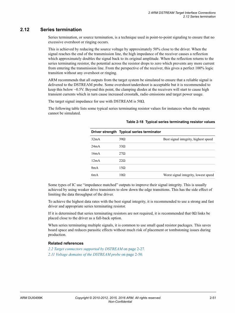
2.12 Series terminationSeries termination, or source termination, is a technique used in point-to-point signaling to ensure that noexcessive overshoot or ringing occurs.
This is achieved by reducing the source voltage by approximately 50% close to the driver. When thesignal reaches the end of the transmission line, the high impedance of the receiver causes a reflectionwhich approximately doubles the signal back to its original amplitude. When the reflection returns to theseries terminating resistor, the potential across the resistor drops to zero which prevents any more currentfrom entering the transmission line. From the perspective of the receiver, this gives a perfect 100% logictransition without any overshoot or ringing.
ARM recommends that all outputs from the target system be simulated to ensure that a reliable signal isdelivered to the DSTREAM probe. Some overshoot/undershoot is acceptable but it is recommended tokeep this below ~0.5V. Beyond this point, the clamping diodes at the receivers will start to cause hightransient currents which in turn cause increased crosstalk, radio emissions and target power usage.
The target signal impedance for use with DSTREAM is 50Ω.
The following table lists some typical series terminating resistor values for instances when the outputscannot be simulated.
Table 2-18 Typical series terminating resistor values
Driver strength Typical series terminator
32mA 39Ω Best signal integrity, highest speed
24mA 33Ω
16mA 27Ω
12mA 22Ω
8mA 15Ω
6mA 10Ω Worst signal integrity, lowest speed
Some types of IC use “impedance matched” outputs to improve their signal integrity. This is usuallyachieved by using weaker drive transistors to slow down the edge transitions. This has the side effect oflimiting the data throughput of the driver.
To achieve the highest data rates with the best signal integrity, it is recommended to use a strong and fastdriver and appropriate series terminating resistor.
If it is determined that series terminating resistors are not required, it is recommended that 0Ω links beplaced close to the driver as a fall-back option.
When series terminating multiple signals, it is common to use small quad resistor packages. This savesboard space and reduces parasitic effects without much risk of placement or tombstoning issues duringproduction.
Related references2.2 Target connectors supported by DSTREAM on page 2-27.2.11 Voltage domains of the DSTREAM probe on page 2-50.
2 ARM DSTREAM Target Interface Connections2.12 Series termination
ARM DUI0499K Copyright © 2010-2012, 2015, 2016 ARM. All rights reserved. 2-51Non-Confidential

Chapter 3ARM DSTREAM User I/O Connections
This describes the additional input and output connections provided in DSTREAM.
It contains the following sections:• 3.1 About the User I/O connector on page 3-53.• 3.2 User I/O pin connections on page 3-54.
ARM DUI0499K Copyright © 2010-2012, 2015, 2016 ARM. All rights reserved. 3-52Non-Confidential
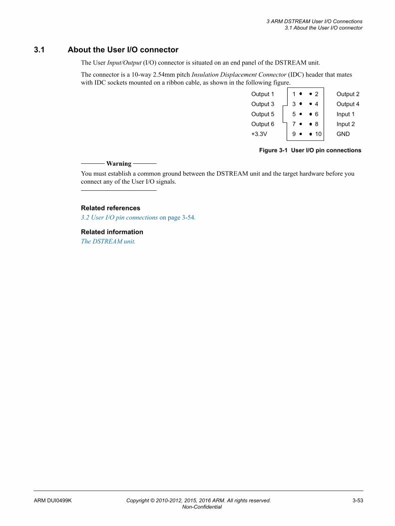
3.1 About the User I/O connectorThe User Input/Output (I/O) connector is situated on an end panel of the DSTREAM unit.
The connector is a 10-way 2.54mm pitch Insulation Displacement Connector (IDC) header that mateswith IDC sockets mounted on a ribbon cable, as shown in the following figure.
1
3
579
2
4
6810
Output 1
Output 3
Output 5Output 6+3.3V
Output 2
Output 4
Input 1Input 2GND
Figure 3-1 User I/O pin connections
Warning
You must establish a common ground between the DSTREAM unit and the target hardware before youconnect any of the User I/O signals.
Related references3.2 User I/O pin connections on page 3-54.
Related informationThe DSTREAM unit.
3 ARM DSTREAM User I/O Connections3.1 About the User I/O connector
ARM DUI0499K Copyright © 2010-2012, 2015, 2016 ARM. All rights reserved. 3-53Non-Confidential

3.2 User I/O pin connectionsThe table shows the User I/O pin connections.
Table 3-1 User I/O pin connections
Pin Signal I/O Description
Pin 1 Output 1 Output This is a user output bit. It operates at a 3.3V swing,with a 100Ω series resistance.
Pin 2 Output 2 Output This is a user output bit. It operates at a 3.3V swing,with a 100Ω series resistance.
Pin 3 Output 3 Output This is a user output bit. It operates at a 3.3V swing,with a 100Ω series resistance.
Pin 4 Output 4 Output This is a user output bit. It operates at a 3.3V swing,with a 100Ω series resistance.
Pin 5 Output 5 Output This is a user output bit. It operates at a 3.3V swing,with a 100Ω series resistance.
Pin 6 Input 1 Input This is a user input bit. It has a 100K weak pull-up tothe unit internal +3.3V supply, and requires a Vih(min)of 2.0V and a Vil(max) of 0.8V. It can safely be drivenby 5V logic levels, and has Electro Static Discharge(ESD) protection greater than the 2kV human bodymodel.
This pin is not currently supported.
Pin 7 Output 6 Output This is a user output bit. It operates at a 3.3V swing,with a 100Ω series resistance.
Pin 8 Input 2 Input This is a copy of the trigger input on the end panel ofthe DSTREAM unit. It has a 10kΩ weak pull-up to theunit internal +3.3V supply, and requires a Vih(min) of2.0V and a Vil(max) of 0.8V. It can safely be driven by5V logic levels, and has ESD protection greater thanthe 2kV human body model.
This pin is not currently supported.
Pin 9 +3.3V Output This is intended as a voltage reference for externalcircuitry and is current limited to approximately50mA.
Pin 10 GND - -
Note
Input is not currently supported on the User I/O pin connections.
3 ARM DSTREAM User I/O Connections3.2 User I/O pin connections
ARM DUI0499K Copyright © 2010-2012, 2015, 2016 ARM. All rights reserved. 3-54Non-Confidential

Chapter 4Target Board Design for Tracing with ARMDSTREAM
This describes the properties of a target board that can be connected to the DSTREAM trace feature.
It contains the following sections:• 4.1 Overview of high-speed design on page 4-56.• 4.2 PCB track impedance on page 4-57.• 4.3 Signal requirements on page 4-58.• 4.4 Probe modeling on page 4-59.
ARM DUI0499K Copyright © 2010-2012, 2015, 2016 ARM. All rights reserved. 4-55Non-Confidential

4.1 Overview of high-speed designFailure to observe high-speed design rules when designing a target system containing an ARMEmbedded Trace Macrocell (ETM) trace port can result in incorrect trace data being captured. You mustgive serious consideration to high-speed signals when designing the target system.
The signals coming from an ETM trace port can have very fast rise and fall times, even at relatively lowfrequencies. For example, a signal with a rise time of 1ns has an effective knee frequency of 500MHzand a signal with a rise time of 500ps has an effective knee frequency of 1GHz (fknee = 0.5/Tr).
Note
These principles apply to all of the trace port signals, but special care must taken with TRACECLK.
You must make the following considerations for high-speed design:
Avoid stubsStubs are short pieces of track that tee off from the main track carrying the signal to, forexample, a test point or a connection to an intermediate device. Stubs cause impedancediscontinuities that affect signal quality and must be avoided.
Special care must therefore be taken when ETM signals are multiplexed with other pin functionsand where the PCB is designed to support both functions with differing tracking requirements.
Minimize signal skew (balancing PCB track lengths)You must attempt to match the lengths of the PCB tracks carrying the trace port signals from theASIC to the Mictor connector to within approximately 0.5 inches (12.5mm) of each other. Anygreater differences directly impact the setup and hold time requirements.
Minimize crosstalkNormal high-speed design rules must be observed. For example, do not run dynamic signalsparallel to each other for any significant distance, keep them spaced well apart, and use a groundplane and so forth. Particular attention must be paid to the TRACECLK signal. If in any doubt,place grounds or static signals between the TRACECLK and any other dynamic signals.
Use impedance matching and terminationAll PCB tracks carrying trace port signals must be impedance matched to approximately 50Ω.Series termination is highly recommended on all high-speed signals.
Related concepts2.12 Series termination on page 2-51.4.4 Probe modeling on page 4-59.
Related references4.2 PCB track impedance on page 4-57.4.3 Signal requirements on page 4-58.
4 Target Board Design for Tracing with ARM DSTREAM4.1 Overview of high-speed design
ARM DUI0499K Copyright © 2010-2012, 2015, 2016 ARM. All rights reserved. 4-56Non-Confidential
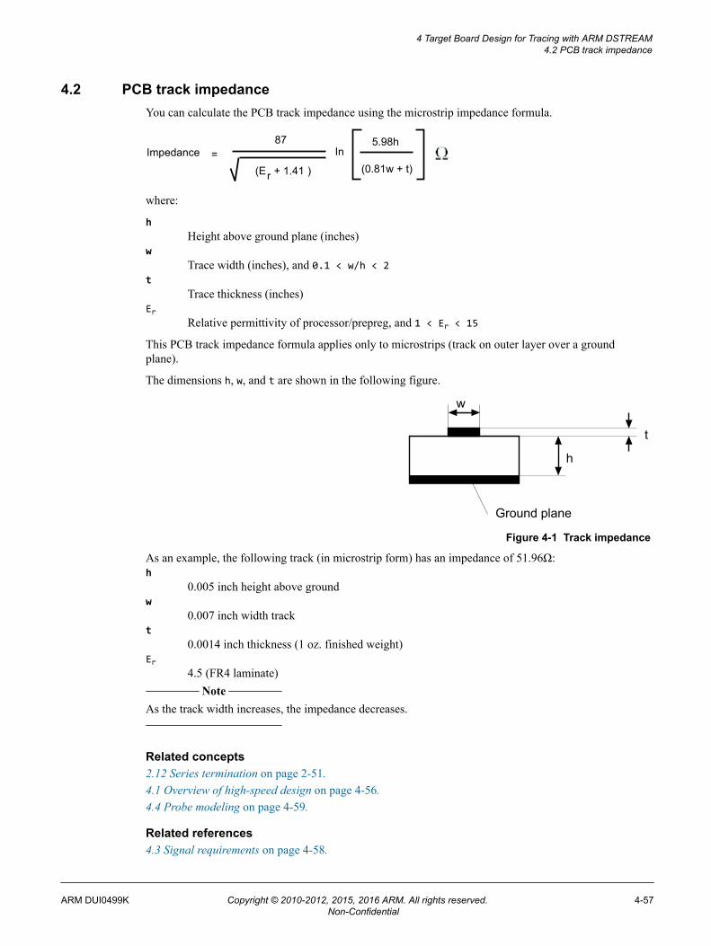
4.2 PCB track impedanceYou can calculate the PCB track impedance using the microstrip impedance formula.
87Impedance = In
(Er + 1.41 ) (0.81w + t)
5.98h
where:
hHeight above ground plane (inches)
wTrace width (inches), and 0.1 < w/h < 2
tTrace thickness (inches)
ErRelative permittivity of processor/prepreg, and 1 < Er < 15
This PCB track impedance formula applies only to microstrips (track on outer layer over a groundplane).
The dimensions h, w, and t are shown in the following figure.
Ground plane
w
h
t
Figure 4-1 Track impedance
As an example, the following track (in microstrip form) has an impedance of 51.96Ω:h
0.005 inch height above groundw
0.007 inch width trackt
0.0014 inch thickness (1 oz. finished weight)Er
4.5 (FR4 laminate) Note
As the track width increases, the impedance decreases.
Related concepts2.12 Series termination on page 2-51.4.1 Overview of high-speed design on page 4-56.4.4 Probe modeling on page 4-59.
Related references4.3 Signal requirements on page 4-58.
4 Target Board Design for Tracing with ARM DSTREAM4.2 PCB track impedance
ARM DUI0499K Copyright © 2010-2012, 2015, 2016 ARM. All rights reserved. 4-57Non-Confidential
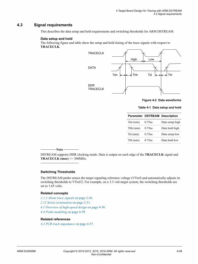
4.3 Signal requirementsThis describes the data setup and hold requirements and switching thresholds for ARM DSTREAM.
Data setup and holdThe following figure and table show the setup and hold timing of the trace signals with respect toTRACECLK.
Tsl ThlThhTsh
TRACECLK
DATA
DDR TRACECLK
High Low
Figure 4-2 Data waveforms
Table 4-1 Data setup and hold
Parameter DSTREAM Description
Tsh (min) 0.75ns Data setup high
Thh (min) 0.75ns Data hold high
Tsl (min) 0.75ns Data setup low
Thl (min) 0.75ns Data hold low
Note
DSTREAM supports DDR clocking mode. Data is output on each edge of the TRACECLK signal andTRACECLK (max) <= 300MHz.
Switching Thresholds
The DSTREAM probe senses the target signaling reference voltage (VTref) and automatically adjusts itsswitching thresholds to VTref/2. For example, on a 3.3 volt target system, the switching thresholds areset to 1.65 volts.
Related concepts2.1.3 About trace signals on page 2-26.2.12 Series termination on page 2-51.4.1 Overview of high-speed design on page 4-56.4.4 Probe modeling on page 4-59.
Related references4.2 PCB track impedance on page 4-57.
4 Target Board Design for Tracing with ARM DSTREAM4.3 Signal requirements
ARM DUI0499K Copyright © 2010-2012, 2015, 2016 ARM. All rights reserved. 4-58Non-Confidential

4.4 Probe modelingFor trace bit rates of 0-600Mbps, basic signal integrity can be established using simplified modeling. Thebulk of the transmission line model consists of the cable being used between the probe and target.
The Mictor cable is made using micro-coax and can be modeled as a 50Ω transmission line with a 1.5nspropagation delay and 0.6Ω DC resistance. The connectors at either end can be modeled as a 0.3pFcapacitance to ground.
The CoreSight/MIPI cables are made using 0.635mm pitch ribbon and can be modeled as a 66Ωtransmission line with a 1.5ns propagation delay and 0.4Ω DC resistance. The connectors at either endcan be modeled as a 0.5pF capacitance to ground.
The JTAG 20 and JTAG 14 cables are made using 1.27mm pitch ribbon and can be modeled as a 100Ωtransmission line with a 1.5ns propagation delay and 0.1Ω DC resistance. The connectors at either endcan be modeled as a 1.0pF capacitance to ground.
The circuit at the probe end of the transmission line can be modeled using the following primitives:• All resistors can be modeled as their ideal resistance values with minimum/zero parasitics.• All capacitors can be modeled as their ideal capacitance values with minimum/zero parasitics.• Input comparators can be modeled using the Spartan 3 SSTLx_I model. The switching threshold can
be assumed to be half of the VTref voltage as supplied by the target and data can be assumed to bevalid when it is 100mV above or below this threshold.
• Output drivers can be modeled using the Spartan 3 LVCMOS Fast 16mA model. The model voltagemust be chosen to match the target system voltage.
All other parasitics and traces within the probe are negligible for most practical purposes.
You are strongly advised to use series termination on all target outputs to achieve good signal integrity.
Related concepts2.12 Series termination on page 2-51.4.1 Overview of high-speed design on page 4-56.
Related references2.10 I/O diagrams for the DSTREAM probe connectors on page 2-48.4.2 PCB track impedance on page 4-57.4.3 Signal requirements on page 4-58.
Related informationARM tools and models.Xilinx.
4 Target Board Design for Tracing with ARM DSTREAM4.4 Probe modeling
ARM DUI0499K Copyright © 2010-2012, 2015, 2016 ARM. All rights reserved. 4-59Non-Confidential