
24lc512
27
© 2005 Microchip Technology Inc. DS21754F-page 1 24AA512/24LC512/24FC512 Device Selection Table Features: • Low-power CMOS technology: - Maximum write current 5 mA at 5.5V - Maximum read current 400 μA at 5.5V - Standby current 100 nA typical at 5.5V • 2-wire serial interface bus, I 2 C ™ compatible • Cascadable for up to eight devices • Self-timed erase/write cycle • 128-byte Page Write mode available • 5 ms max. write cycle time • Hardware write-protect for entire array • Schmitt Trigger inputs for noise suppression • 1,000,000 erase/write cycles • Electrostatic discharge protection > 4000V • Data retention > 200 years • 8-pin PDIP, SOIC (208 mil), and DFN packages • 14-lead TSSOP package • Standard and Pb-free finishes available • Temperature ranges: Description: The Microchip Technology Inc. 24AA512/24LC512/ 24FC512 (24XX512*) is a 64K x 8 (512 Kbit) Serial Electrically Erasable PROM, capable of operation across a broad voltage range (1.8V to 5.5V). It has been developed for advanced, low-power applications such as personal communications and data acquisi- tion. This device also has a page write capability of up to 128 bytes of data. This device is capable of both random and sequential reads up to the 512K boundary. Functional address lines allow up to eight devices on the same bus, for up to 4 Mbit address space. This device is available in the standard 8-pin plastic DIP, SOIC, DFN and 14-lead TSSOP packages. Block Diagram Package Type Part Number VCC Range Max. Clock Frequency Temp. Ranges 24AA512 1.8-5.5V 400 kHz (1) I 24LC512 2.5-5.5V 400 kHz I, E 24FC512 2.5-5.5V 1 MHz I Note 1: 100 kHz for VCC < 2.5V - Industrial (I): -40°C to +85°C - Automotive (E): -40°C to +125°C HV Generator EEPROM Array Page Latches YDEC XDEC Sense Amp. R/W Control Memory Control Logic I/O Control Logic I/O A0 A1 A2 SDA SCL VCC VSS WP A0 A1 A2 VSS VCC WP SCL SDA 1 2 3 4 8 7 6 5 24XX512 PDIP SOIC A0 A1 A2 VSS 1 2 3 4 8 7 6 5 VCC WP SCL SDA TSSOP 24XX512 DFN A0 A1 A2 VSS WP SCL SDA 24XX512 5 6 7 8 4 3 2 1 VCC NC A0 A1 NC A2 VSS NC NC VCC WP NC SCL SDA NC 24XX512 1 2 3 4 14 13 12 11 5 10 6 9 7 8 512K I 2 C ™ CMOS Serial EEPROM * 24XX512 is used in this document as a generic part number for the 24AA512/24LC512/24FC512 devices.
-
Upload
jeziel-vazquez-nava -
Category
Documents
-
view
21 -
download
0
description
eeproom memory to use in electronic circuits
Transcript of 24lc512

24AA512/24LC512/24FC512512K I2C™ CMOS Serial EEPROM
Device Selection Table
Features:
• Low-power CMOS technology:
- Maximum write current 5 mA at 5.5V- Maximum read current 400 μA at 5.5V- Standby current 100 nA typical at 5.5V
• 2-wire serial interface bus, I2C™ compatible• Cascadable for up to eight devices • Self-timed erase/write cycle
• 128-byte Page Write mode available• 5 ms max. write cycle time• Hardware write-protect for entire array
• Schmitt Trigger inputs for noise suppression• 1,000,000 erase/write cycles• Electrostatic discharge protection > 4000V
• Data retention > 200 years• 8-pin PDIP, SOIC (208 mil), and DFN packages• 14-lead TSSOP package
• Standard and Pb-free finishes available• Temperature ranges:
Description:
The Microchip Technology Inc. 24AA512/24LC512/24FC512 (24XX512*) is a 64K x 8 (512 Kbit) SerialElectrically Erasable PROM, capable of operationacross a broad voltage range (1.8V to 5.5V). It hasbeen developed for advanced, low-power applicationssuch as personal communications and data acquisi-tion. This device also has a page write capability of upto 128 bytes of data. This device is capable of bothrandom and sequential reads up to the 512K boundary.Functional address lines allow up to eight devices onthe same bus, for up to 4 Mbit address space. Thisdevice is available in the standard 8-pin plastic DIP,SOIC, DFN and 14-lead TSSOP packages.
Block Diagram
Package Type
Part Number
VCC
RangeMax. ClockFrequency
Temp. Ranges
24AA512 1.8-5.5V 400 kHz(1) I
24LC512 2.5-5.5V 400 kHz I, E
24FC512 2.5-5.5V 1 MHz I
Note 1: 100 kHz for VCC < 2.5V
- Industrial (I): -40°C to +85°C- Automotive (E): -40°C to +125°C
HV Generator
EEPROM Array
Page Latches
YDEC
XDEC
Sense Amp.R/W Control
MemoryControl
Logic
I/OControlLogic
I/O
A0 A1 A2
SDA
SCL
VCC
VSS
WP
A0
A1
A2
VSS
VCC
WP
SCL
SDA
1
2
3
4
8
7
6
5
24X
X51
2
PDIP SOIC
A0
A1
A2
VSS
1
2
3
4
8
7
6
5
VCC
WP
SCL
SDA
TSSOP
24X
X51
2
DFN
A0
A1
A2
VSS
WP
SCL
SDA
24X
X51
2
5
6
7
8
4
3
2
1 VCC
NC
A0A1
NC
A2VSS
NC
NC
VCC
WP
NC
SCLSDA
NC
24X
X51
2
1234
14131211
5 106 97 8
* 24XX512 is used in this document as a generic part number for the 24AA512/24LC512/24FC512 devices.
© 2005 Microchip Technology Inc. DS21754F-page 1

24AA512/24LC512/24FC512
1.0 ELECTRICAL CHARACTERISTICS
Absolute Maximum Ratings (†)
VCC.............................................................................................................................................................................6.5V
All inputs and outputs w.r.t. VSS ......................................................................................................... -0.6V to VCC +1.0V
Storage temperature ...............................................................................................................................-65°C to +150°C
Ambient temperature with power applied................................................................................................-40°C to +125°C
ESD protection on all pins ......................................................................................................................................................≥ 4 kV
TABLE 1-1: DC CHARACTERISTICS
† NOTICE: Stresses above those listed under “Absolute Maximum Ratings” may cause permanent damage to thedevice. This is a stress rating only and functional operation of the device at those or any other conditions above thoseindicated in the operational listings of this specification is not implied. Exposure to maximum rating conditions forextended periods may affect device reliability.
DC CHARACTERISTICSElectrical Characteristics:Industrial (I): VCC = +1.8V to 5.5V TA = -40°C to +85°CAutomotive (E): VCC = +2.5V to 5.5V TA = -40°C to +125°C
Param.No.
Sym Characteristic Min Max Units Conditions
D1 — A0, A1, A2, SCL, SDA and WP pins:
— — — —
D2 VIH High-level input voltage 0.7 VCC — V —
D3 VIL Low-level input voltage — 0.3 VCC
0.2 VCC
VV
VCC ≥ 2.5VVCC < 2.5V
D4 VHYS Hysteresis of Schmitt Trigger inputs(SDA, SCL pins)
0.05 VCC — V VCC ≥ 2.5V (Note)
D5 VOL Low-level output voltage — 0.40 V IOL = 3.0 ma @ VCC = 4.5VIOL = 2.1 ma @ VCC = 2.5V
D6 ILI Input leakage current — ±1 μA VIN = VSS or VCC, WP = VSS
VIN = VSS or VCC, WP = VCC
D7 ILO Output leakage current — ±1 μA VOUT = VSS or VCC
D8 CIN, COUT
Pin capacitance (all inputs/outputs)
— 10 pF VCC = 5.0V (Note)TA = 25°C, fC = 1 MHz
D9 ICC Read Operating current — 400 μA VCC = 5.5V, SCL = 400 kHz
ICC Write — 5 mA VCC = 5.5V
D10 ICCS Standby current — 1 μA TA = -40°C to +85°CSCL = SDA = VCC = 5.5VA0, A1, A2, WP = VSS
— 5 μA TA = -40°C to +125°CSCL = SDA = VCC = 5.5VA0, A1, A2, WP = VSS
Note: This parameter is periodically sampled and not 100% tested.
DS21754F-page 2 © 2005 Microchip Technology Inc.

24AA512/24LC512/24FC512
TABLE 1-2: AC CHARACTERISTICS
AC CHARACTERISTICSElectrical Characteristics:Industrial (I): VCC = +1.8V to 5.5V TA = -40°C to +85°CAutomotive (E): VCC = +2.5V to 5.5V TA = -40°C to +125°C
Param.No.
Sym Characteristic Min Max Units Conditions
1 FCLK Clock frequency ———
100400
1000
kHz 1.8V ≤ VCC < 2.5V2.5V ≤ VCC ≤ 5.5V2.5V ≤ VCC ≤ 5.5V 24FC512
2 THIGH Clock high time 4000600500
———
ns 1.8V ≤ VCC < 2.5V2.5V ≤ VCC ≤ 5.5V2.5V ≤ VCC ≤ 5.5V 24FC512
3 TLOW Clock low time 47001300500
———
ns 1.8V ≤ VCC < 2.5V2.5V ≤ VCC ≤ 5.5V2.5V ≤ VCC ≤ 5.5V 24FC512
4 TR SDA and SCL rise time (Note 1) ———
1000300300
ns 1.8V ≤ VCC< 2.5V2.5V ≤ VCC ≤ 5.5V2.5V ≤ VCC ≤ 5.5V 24FC512
5 TF SDA and SCL fall time (Note 1) ——
300100
ns All except, 24FC5122.5V ≤ VCC ≤ 5.5V 24FC512
6 THD:STA Start condition hold time 4000600250
———
ns 1.8V ≤ VCC < 2.5V2.5V ≤ VCC ≤ 5.5V2.5V ≤ VCC ≤ 5.5V 24FC512
7 TSU:STA Start condition setup time 4700600250
———
ns 1.8V ≤ VCC < 2.5V2.5V ≤ VCC ≤ 5.5V2.5V ≤ VCC ≤ 5.5V 24FC512
8 THD:DAT Data input hold time 0 — ns (Note 2)
9 TSU:DAT Data input setup time 250100100
———
ns 1.8V ≤ VCC < 2.5V2.5V ≤ VCC ≤ 5.5V2.5V ≤ VCC ≤ 5.5V 24FC512
10 TSU:STO Stop condition setup time 4000600250
———
ns 1.8V ≤ VCC < 2.5V2.5V ≤ VCC ≤ 5.5V2.5V ≤ VCC ≤ 5.5V 24FC512
11 TSU:WP WP setup time 4000600600
———
ns 1.8V ≤ VCC < 2.5V2.5V ≤ VCC ≤ 5.5V2.5V ≤ VCC ≤ 5.5V 24FC512
12 THD:WP WP hold time 470013001300
———
ns 1.8V ≤ VCC < 2.5V2.5V ≤ VCC ≤ 5.5V2.5V ≤ VCC ≤ 5.5V 24FC512
13 TAA Output valid from clock (Note 2) ———
3500900400
ns 1.8V ≤ VCC < 2.5V2.5V ≤ VCC ≤ 5.5V2.5V ≤ VCC ≤ 5.5V 24FC512
14 TBUF Bus free time: Time the bus must be free before a new trans-mission can start
47001300500
———
ns 1.8V ≤ VCC < 2.5V2.5V ≤ VCC ≤ 5.5V2.5V ≤ VCC ≤ 5.5V 24FC512
16 TSP Input filter spike suppression(SDA and SCL pins)
— 50 ns All except, 24FC512 (Notes 1 and 3)
17 TWC Write cycle time (byte or page) — 5 ms —
18 — Endurance 1,000,000 — cycles 25°C (Note 4)
Note 1: Not 100% tested. CB = total capacitance of one bus line in pF.2: As a transmitter, the device must provide an internal minimum delay time to bridge the undefined region (minimum
300 ns) of the falling edge of SCL to avoid unintended generation of Start or Stop conditions.3: The combined TSP and VHYS specifications are due to new Schmitt Trigger inputs which provide improved noise spike
suppression. This eliminates the need for a TI specification for standard operation.4: This parameter is not tested but ensured by characterization. For endurance estimates in a specific application, please
consult the Total Endurance™ Model which can be obtained from Microchip’s web site: www.microchip.com.
© 2005 Microchip Technology Inc. DS21754F-page 3

24AA512/24LC512/24FC512
FIGURE 1-1: BUS TIMING DATA
(unprotected)(protected)
SCL
SDAIN
SDAOUT
WP
5
7
6
16
3
2
8 9
13
D4 4
10
11 12
14
DS21754F-page 4 © 2005 Microchip Technology Inc.

24AA512/24LC512/24FC512
2.0 PIN DESCRIPTIONS
The descriptions of the pins are listed in Table 2-1.
TABLE 2-1: PIN FUNCTION TABLE
2.1 A0, A1 and A2 Chip Address Inputs
The A0, A1 and A2 inputs are used by the 24XX512 formultiple device operations. The logic levels on theseinputs are compared with the corresponding bits in theslave address. The chip is selected if the compare istrue.
Up to eight devices may be connected to the same busby using different Chip Select bit combinations. If thesepins are left unconnected, the inputs will be pulleddown internally to VSS. If they are tied to VCC or drivenhigh, the internal pull-down circuitry is disabled.
In most applications, the chip address inputs A0, A1,and A2 are hard-wired to logic ‘0’ or logic ‘1’. Forapplications in which these pins are controlled by amicrocontroller or other programmable logic device,the chip address pins must be driven to logic ‘0’ or logic‘1’ before normal device operation can proceed.
2.2 Serial Data (SDA)
This is a bidirectional pin used to transfer addressesand data into and data out of the device. It is an open-drain terminal, therefore, the SDA bus requires a pull-up resistor to VCC (typical 10 kΩ for 100 kHz, 2 kΩ for400 kHz and 1 MHz).
For normal data transfer, SDA is allowed to changeonly during SCL low. Changes during SCL high arereserved for indicating the Start and Stop conditions.
2.3 Serial Clock (SCL)
This input is used to synchronize the data transfer fromand to the device.
2.4 Write-Protect (WP)
This pin can be connected to either VSS or VCC.Internal pull-down circuitry on this pin will keep thedevice in the unprotected state if left floating, however,floating this pin is not recommended for mostapplications. If tied to VSS, normal memory operation isenabled (read/write the entire memory 0000-FFFF).
If tied to VCC, write operations are inhibited. Readoperations are not affected.
3.0 FUNCTIONAL DESCRIPTION
The 24XX512 supports a bidirectional 2-wire bus anddata transmission protocol. A device that sends dataonto the bus is defined as a transmitter and a devicereceiving data as a receiver. The bus must becontrolled by a master device which generates theserial clock (SCL), controls the bus access andgenerates the Start and Stop conditions, while the24XX512 works as a slave. Both master and slavecan operate as a transmitter or receiver, but themaster device determines which mode is activated.
Name PDIP SOIC14-leadTSSOP
DFN Function
A0 1 1 1 1 User Configured Chip Select
A1 2 2 2 2 User Configured Chip Select
(NC) — — 3, 4, 5 — Not Connected
A2 3 3 6 3 User Configured Chip Select
VSS 4 4 7 4 Ground
SDA 5 5 8 5 Serial Data
SCL 6 6 9 6 Serial Clock
(NC) — — 10, 11, 12 — Not Connected
WP 7 7 13 7 Write-Protect Input
VCC 8 8 14 8 +1.8V to 5.5V (24AA512)+2.5V to 5.5V (24LC512)+2.5V to 5.5V (24FC512)
© 2005 Microchip Technology Inc. DS21754F-page 5

24AA512/24LC512/24FC512
4.0 BUS CHARACTERISTICS
The following bus protocol has been defined:
• Data transfer may be initiated only when the bus is not busy.
• During data transfer, the data line must remain stable whenever the clock line is high. Changes in the data line, while the clock line is high, will be interpreted as a Start or Stop condition.
Accordingly, the following bus conditions have beendefined (Figure 4-1).
4.1 Bus Not Busy (A)
Both data and clock lines remain high.
4.2 Start Data Transfer (B)
A high-to-low transition of the SDA line while the clock(SCL) is high determines a Start condition. Allcommands must be preceded by a Start condition.
4.3 Stop Data Transfer (C)
A low-to-high transition of the SDA line while the clock(SCL) is high determines a Stop condition. Alloperations must end with a Stop condition.
4.4 Data Valid (D)
The state of the data line represents valid data when,after a Start condition, the data line is stable for theduration of the high period of the clock signal.
The data on the line must be changed during the lowperiod of the clock signal. There is one bit of data perclock pulse.
Each data transfer is initiated with a Start condition andterminated with a Stop condition. The number of thedata bytes transferred between the Start and Stopconditions is determined by the master device.
4.5 Acknowledge
Each receiving device, when addressed, is obliged togenerate an Acknowledge signal after the reception ofeach byte. The master device must generate an extraclock pulse which is associated with this Acknowledgebit. See Figure 4-2 for acknowledge timing.
A device that acknowledges must pull down the SDAline during the Acknowledge clock pulse in such a waythat the SDA line is stable low during the high period ofthe acknowledge related clock pulse. Of course, setupand hold times must be taken into account. Duringreads, a master must signal an end of data to the slaveby NOT generating an Acknowledge bit on the last bytethat has been clocked out of the slave. In this case, theslave (24XX512) will leave the data line high to enablethe master to generate the Stop condition.
Note: The 24XX512 does not generate anyAcknowledge bits if an internal programmingcycle is in progress.
DS21754F-page 6 © 2005 Microchip Technology Inc.

24AA512/24LC512/24FC512
FIGURE 4-1: DATA TRANSFER SEQUENCE ON THE SERIAL BUS
FIGURE 4-2: ACKNOWLEDGE TIMING
Address orAcknowledge
Valid
DataAllowed
to Change
StopCondition
StartCondition
SCL
SDA
(A) (B) (D) (D) (C) (A)
SCL 987654321 1 2 3
Transmitter must release the SDA line at this pointallowing the Receiver to pull the SDA line low toacknowledge the previous eight bits of data.
Receiver must release the SDA lineat this point so the Transmitter cancontinue sending data.
Data from transmitterSDA
AcknowledgeBit
Data from transmitter
© 2005 Microchip Technology Inc. DS21754F-page 7

24AA512/24LC512/24FC512
5.0 DEVICE ADDRESSING
A control byte is the first byte received following theStart condition from the master device (Figure 5-1).The control byte consists of a 4-bit control code; for the24XX512 this is set as ‘1010’ binary for read and writeoperations. The next three bits of the control byte arethe Chip Select bits (A2, A1 and A0). The Chip Selectbits allow the use of up to eight 24XX512 devices onthe same bus and are used to select which device isaccessed. The Chip Select bits in the control byte mustcorrespond to the logic levels on the corresponding A2,A1 and A0 pins for the device to respond. These bitsare in effect the three Most Significant bits of the wordaddress.
The last bit of the control byte defines the operation tobe performed. When set to a one a read operation isselected and when set to a zero a write operation isselected. The next two bytes received define theaddress of the first data byte (Figure 5-2). Because allA15…A0 are used, there are no upper address bits thatare “don’t care”. The upper address bits are transferredfirst, followed by the Less Significant bits.
Following the Start condition, the 24XX512 monitorsthe SDA bus checking the device type identifier beingtransmitted. Upon receiving a ‘1010’ code and appro-priate device select bits, the slave device outputs anAcknowledge signal on the SDA line. Depending on thestate of the R/W bit, the 24XX512 will select a read orwrite operation.
FIGURE 5-1: CONTROL BYTE FORMAT
5.1 Contiguous Addressing Across Multiple Devices
The Chip Select bits A2, A1 and A0 can be used toexpand the contiguous address space for up to 4 Mbitby adding up to eight 24XX512s on the same bus. Inthis case, software can use A0 of the control byte asaddress bit A16; A1, as address bit A17; and A2, asaddress bit A18. It is not possible to sequentially readacross device boundaries.
FIGURE 5-2: ADDRESS SEQUENCE BIT ASSIGNMENTS
1 0 1 0 A2 A1 A0S ACKR/W
Control CodeChip Select
Bits
Slave Address
Acknowledge BitStart Bit
Read/Write Bit
1 0 1 0A2
A1
A0 R/W A
11A10
A9
A7
A0
A8 • • • • • •
A12
CONTROL BYTE ADDRESS HIGH BYTE ADDRESS LOW BYTE
CONTROLCODE
CHIPSELECT
BITS
A13
A14
A15
DS21754F-page 8 © 2005 Microchip Technology Inc.
24AA512/24LC512/24FC512
6.0 WRITE OPERATIONS
6.1 Byte Write
Following the Start condition from the master, thecontrol code (four bits), the Chip Select (three bits) andthe R/W bit (which is a logic low) are clocked onto thebus by the master transmitter. This indicates to theaddressed slave receiver that the address high byte willfollow after it has generated an Acknowledge bit duringthe ninth clock cycle. Therefore, the next bytetransmitted by the master is the high-order byte of theword address and will be written into the addresspointer of the 24XX512. The next byte is the LeastSignificant Address byte. After receiving anotherAcknowledge signal from the 24XX512, the masterdevice will transmit the data word to be written into theaddressed memory location. The 24XX512 acknowl-edges again and the master generates a Stopcondition. This initiates the internal write cycle andduring this time, the 24XX512 will not generateAcknowledge signals (Figure 6-1). If an attempt ismade to write to the array with the WP pin held high, thedevice will acknowledge the command, but no writecycle will occur, no data will be written and the devicewill immediately accept a new command. After a ByteWrite command, the internal address counter will pointto the address location following the one that was justwritten.
6.2 Page Write
The write control byte, word address and the first databyte are transmitted to the 24XX512 in the same wayas in a byte write. But instead of generating a Stopcondition, the master transmits up to 127 additionalbytes, which are temporarily stored in the on-chip pagebuffer and will be written into memory after the masterhas transmitted a Stop condition. After receipt of eachword, the seven lower address pointer bits are inter-nally incremented by one. If the master should transmitmore than 128 bytes prior to generating the Stop con-dition, the address counter will roll over and the previ-ously received data will be overwritten. As with the bytewrite operation, once the Stop condition is received, aninternal write cycle will begin (Figure 6-2). If an attemptis made to write to the array with the WP pin held high,the device will acknowledge the command, but no writecycle will occur, no data will be written and the devicewill immediately accept a new command.
6.3 Write Protection
The WP pin allows the user to write-protect the entirearray (0000-FFFF) when the pin is tied to VCC. If tied toVSS or left floating, the write protection is disabled. TheWP pin is sampled at the Stop bit for every Writecommand (Figure 1-1). Toggling the WP pin after theStop bit will have no effect on the execution of the writecycle.
Note: Page write operations are limited to writingbytes within a single physical page,regardless of the number of bytesactually being written. Physical pageboundaries start at addresses that areinteger multiples of the page buffer size (or‘page size’) and end at addresses that areinteger multiples of [page size – 1]. If aPage Write command attempts to writeacross a physical page boundary, theresult is that the data wraps around to thebeginning of the current page (overwritingdata previously stored there), instead ofbeing written to the next page as might beexpected. It is therefore necessary for theapplication software to prevent page writeoperations that would attempt to cross apage boundary.
© 2005 Microchip Technology Inc. DS21754F-page 9

24AA512/24LC512/24FC512
FIGURE 6-1: BYTE WRITE
FIGURE 6-2: PAGE WRITE
BUS ACTIVITYMASTER
SDA LINE
BUS ACTIVITY
START
CONTROLBYTE
ADDRESSHIGH BYTE
ADDRESSLOW BYTE DATA
STOP
ACK
ACK
ACK
ACK
S 1 0 1 0 0A2
A1
A0 P
BUS ACTIVITYMASTER
SDA LINE
BUS ACTIVITY
START
CONTROLBYTE
ADDRESSHIGH BYTE
ADDRESSLOW BYTE DATA BYTE 0
STOP
ACK
ACK
ACK
ACK
DATA BYTE 127
ACK
S 1 0 1 0 0A2
A1
A0 P
DS21754F-page 10 © 2005 Microchip Technology Inc.
24AA512/24LC512/24FC512
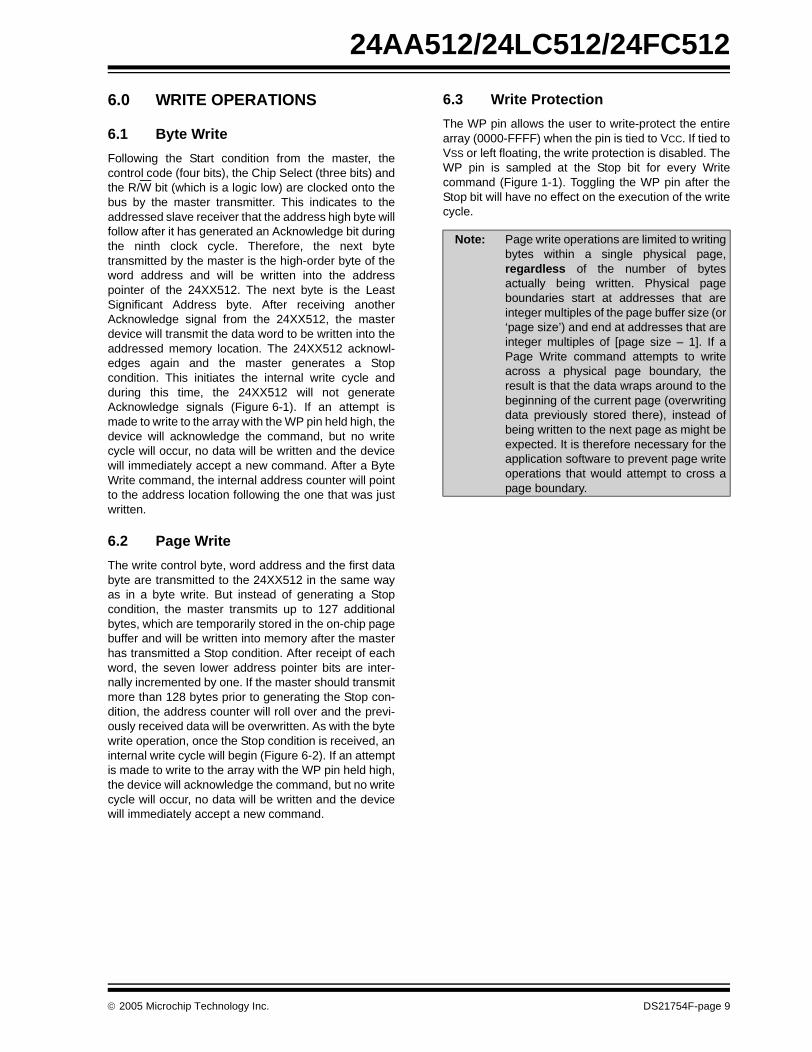
7.0 ACKNOWLEDGE POLLING
Since the device will not acknowledge during a writecycle, this can be used to determine when the cycle iscomplete (this feature can be used to maximize busthroughput). Once the Stop condition for a Writecommand has been issued from the master, the deviceinitiates the internally timed write cycle. ACK pollingcan be initiated immediately. This involves the mastersending a Start condition, followed by the control bytefor a Write command (R/W = 0). If the device is stillbusy with the write cycle, then no ACK will be returned.If no ACK is returned, then the Start bit and control bytemust be resent. If the cycle is complete, then the devicewill return the ACK and the master can then proceedwith the next Read or Write command. See Figure 7-1for flow diagram.
FIGURE 7-1: ACKNOWLEDGE POLLING FLOW
SendWrite Command
Send StopCondition to
Initiate Write Cycle
Send Start
Send Control Bytewith R/W = 0
Did DeviceAcknowledge
(ACK = 0)?
NextOperation
No
Yes
© 2005 Microchip Technology Inc. DS21754F-page 11

24AA512/24LC512/24FC512
8.0 READ OPERATION
Read operations are initiated in the same way as writeoperations with the exception that the R/W bit of thecontrol byte is set to ‘1’. There are three basic types ofread operations: current address read, random readand sequential read.
8.1 Current Address Read
The 24XX512 contains an address counter that main-tains the address of the last word accessed, internallyincremented by ‘1’. Therefore, if the previous readaccess was to address n (n is any legal address), thenext current address read operation would access datafrom address n + 1.
Upon receipt of the control byte with R/W bit set to ‘1’,the 24XX512 issues an acknowledge and transmits the8-bit data word. The master will not acknowledge thetransfer but does generate a Stop condition and the24XX512 discontinues transmission (Figure 8-1).
FIGURE 8-1: CURRENT ADDRESS READ
8.2 Random Read
Random read operations allow the master to accessany memory location in a random manner. To performthis type of read operation, first the word address mustbe set. This is done by sending the word address to the24XX512 as part of a write operation (R/W bit set to‘0’). After the word address is sent, the mastergenerates a Start condition following the acknowledge.This terminates the write operation, but not before theinternal address pointer is set. Then, the master issuesthe control byte again but with the R/W bit set to a one.The 24XX512 will then issue an acknowledge andtransmit the 8-bit data word. The master will notacknowledge the transfer but does generate a Stopcondition which causes the 24XX512 to discontinuetransmission (Figure 8-2). After a random Readcommand, the internal address counter will point to theaddress location following the one that was just read.
8.3 Sequential Read
Sequential reads are initiated in the same way as arandom read except that after the 24XX512 transmitsthe first data byte, the master issues an acknowledgeas opposed to the Stop condition used in a randomread. This acknowledge directs the 24XX512 totransmit the next sequentially addressed 8-bit word(Figure 8-3). Following the final byte transmitted to themaster, the master will NOT generate an acknowledge,but will generate a Stop condition. To providesequential reads, the 24XX512 contains an internaladdress pointer which is incremented by one at thecompletion of each operation. This address pointerallows the entire memory contents to be serially readduring one operation. The internal address pointer willautomatically roll over from address FFFF to address0000 if the master acknowledges the byte receivedfrom the array address FFFF.
BUS ACTIVITYMASTER
SDA LINE
BUS ACTIVITY
PS
STOP
CONTROLBYTE
START
DATA
ACK
NO
ACK
1 10 0 A A A 1
BYTE
2 1 0
DS21754F-page 12 © 2005 Microchip Technology Inc.

24AA512/24LC512/24FC512
FIGURE 8-2: RANDOM READ
FIGURE 8-3: SEQUENTIAL READ
BUS ACTIVITY MASTER
SDA LINE
BUS ACTIVITYACK
NOACK
ACK
ACK
ACK
STOP
START
CONTROLBYTE
ADDRESSHIGH BYTE
ADDRESSLOW BYTE
CONTROLBYTE
DATABYTE
START
X = “don’t care” bit
S 1 0 1 0 A A A 02 1 0 S 1 0 1 0 A A A 12 1 0 P
BUS ACTIVITY MASTER
SDA LINE
BUS ACTIVITY
CONTROLBYTE DATA (n) DATA (n + 1) DATA (n + 2) DATA (n + X)
NOACK
ACK
ACK
ACK
ACK
STOP
P
© 2005 Microchip Technology Inc. DS21754F-page 13

24AA512/24LC512/24FC512
9.0 PACKAGING INFORMATION
9.1 Package Marking Information
XXXXXXXXT/XXXNNN
YYWW
8-Lead PDIP (300 mil) Example:
8-Lead SOIC (208 mil) Example:
24LC512
0510017I/SM
24AA512I/P 017
0510
XXXXXXXX
YYWWNNNT/XXXXXX
8-Lead DFN-S Example:
XXXXXXXT/XXXXXYYWW
24LC512I/MF
0510017NNN
14-Lead TSSOP Example:
XXXXXXXTYYWW
NNN
4L512I0510
017
*Standard device marking consists of Microchip part number, year code, week code, and traceability code. Fordevice marking beyond this, certain price adders apply. Please check with your Microchip Sales Office.
Legend: XX...X Customer-specific information*Y Year code (last digit of calendar year)YY Year code (last 2 digits of calendar year)WW Week code (week of January 1 is week ‘01’)NNN Alphanumeric traceability code Pb-free JEDEC designator for Matte Tin (Sn)* This package is Pb-free. The Pb-free JEDEC designator ( )
can be found on the outer packaging for this package.T TemperatureBlank CommercialI IndustrialE Extended
Note: In the event the full Microchip part number cannot be marked on one line, it willbe carried over to the next line, thus limiting the number of availablecharacters for customer-specific information.
3e
3e
3e
3e
3e
DS21754F-page 14 © 2005 Microchip Technology Inc.
24AA512/24LC512/24FC512
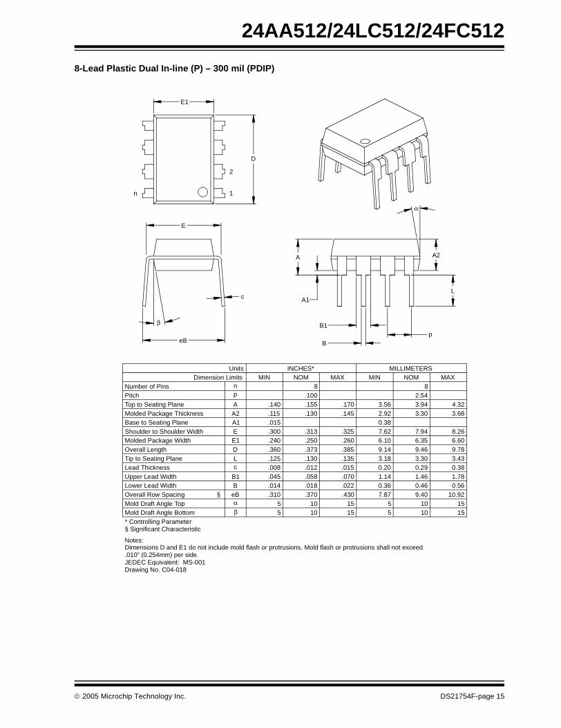
8-Lead Plastic Dual In-line (P) – 300 mil (PDIP)
B1
B
A1
A
L
A2
p
α
E
eB
β
c
E1
n
D
1
2
Units INCHES* MILLIMETERSDimension Limits MIN NOM MAX MIN NOM MAX
Number of Pins n 8 8Pitch p .100 2.54Top to Seating Plane A .140 .155 .170 3.56 3.94 4.32Molded Package Thickness A2 .115 .130 .145 2.92 3.30 3.68Base to Seating Plane A1 .015 0.38Shoulder to Shoulder Width E .300 .313 .325 7.62 7.94 8.26Molded Package Width E1 .240 .250 .260 6.10 6.35 6.60Overall Length D .360 .373 .385 9.14 9.46 9.78Tip to Seating Plane L .125 .130 .135 3.18 3.30 3.43Lead Thickness c .008 .012 .015 0.20 0.29 0.38Upper Lead Width B1 .045 .058 .070 1.14 1.46 1.78Lower Lead Width B .014 .018 .022 0.36 0.46 0.56Overall Row Spacing § eB .310 .370 .430 7.87 9.40 10.92Mold Draft Angle Top α 5 10 15 5 10 15Mold Draft Angle Bottom β 5 10 15 5 10 15* Controlling Parameter
Notes:Dimensions D and E1 do not include mold flash or protrusions. Mold flash or protrusions shall not exceed
JEDEC Equivalent: MS-001Drawing No. C04-018
.010” (0.254mm) per side.
§ Significant Characteristic
© 2005 Microchip Technology Inc. DS21754F-page 15

24AA512/24LC512/24FC512
8-Lead Plastic Small Outline (SM) – Medium, 208 mil (SOIC)
Foot Angle φ 0 4 8 0 4 8
1512015120βMold Draft Angle Bottom1512015120αMold Draft Angle Top
0.510.430.36.020.017.014BLead Width0.250.230.20.010.009.008cLead Thickness
0.760.640.51.030.025.020LFoot Length5.335.215.13.210.205.202DOverall Length5.385.285.11.212.208.201E1Molded Package Width8.267.957.62.325.313.300EOverall Width0.250.130.05.010.005.002A1Standoff §1.98.078A2Molded Package Thickness2.03.080AOverall Height
1.27.050pPitch88nNumber of Pins
MAXNOMMINMAXNOMMINDimension LimitsMILLIMETERSINCHES*Units
α
A2A
A1L
c
β
φ
2
1
D
n
p
B
E
E1
.070 .075
.069 .0741.781.75
1.971.88
* Controlling Parameter
Notes:Dimensions D and E1 do not include mold flash or protrusions. Mold flash or protrusions shall not exceed .010” (0.254mm) per side.Drawing No. C04-056
§ Significant Characteristic
DS21754F-page 16 © 2005 Microchip Technology Inc.

24AA512/24LC512/24FC512
8-Lead Plastic Dual Flat No Lead Package (MF) 6x5 mm Body (DFN-S) – Saw Singulated
© 2005 Microchip Technology Inc. DS21754F-page 17

24AA512/24LC512/24FC512
14-Lead Plastic Thin Shrink Small Outline (ST) – 4.4 mm (TSSOP)
840840φFoot Angle
10501050βMold Draft Angle Bottom10501050αMold Draft Angle Top
0.300.250.19.012.010.007BLead Width0.200.150.09.008.006.004cLead Thickness
0.700.600.50.028.024.020LFoot Length5.105.004.90.201.197.193DMolded Package Length4.504.404.30.177.173.169E1Molded Package Width6.506.386.25.256.251.246EOverall Width0.150.100.05.006.004.002A1Standoff §0.950.900.85.037.035.033A2Molded Package Thickness1.10.043AOverall Height
0.65.026pPitch1414nNumber of Pins
MAXNOMMINMAXNOMMINDimension LimitsMILLIMETERS*INCHESUnits
Lβ
c
φ
2
1
D
nB
p
E1
E
α
A2A1
A
* Controlling Parameter
Notes:Dimensions D and E1 do not include mold flash or protrusions. Mold flash or protrusions shall not exceed .005” (0.127mm) per side.JEDEC Equivalent: MO-153Drawing No. C04-087
§ Significant Characteristic
DS21754F-page 18 © 2005 Microchip Technology Inc.

24AA512/24LC512/24FC512
APPENDIX A: REVISION HISTORY
Revision D
Correction to Section 1.0, Electrical Characteristics.
Revision E
Correction to Section 1.0., Ambient Temperature Correction to Section 6.2, Page Write
Revision F
Add E3 (Pb-free) to marking examples.Updated Marking Legend and On-line Support.
© 2005 Microchip Technology Inc. DS21754F-page 19

24AA512/24LC512/24FC512
NOTES:
DS21754F-page 20 © 2005 Microchip Technology Inc.

24AA512/24LC512/24FC512
THE MICROCHIP WEB SITE
Microchip provides online support via our WWW site atwww.microchip.com. This web site is used as a meansto make files and information easily available tocustomers. Accessible by using your favorite Internetbrowser, the web site contains the followinginformation:
• Product Support – Data sheets and errata, application notes and sample programs, design resources, user’s guides and hardware support documents, latest software releases and archived software
• General Technical Support – Frequently Asked Questions (FAQ), technical support requests, online discussion groups, Microchip consultant program member listing
• Business of Microchip – Product selector and ordering guides, latest Microchip press releases, listing of seminars and events, listings of Microchip sales offices, distributors and factory representatives
CUSTOMER CHANGE NOTIFICATION SERVICE
Microchip’s customer notification service helps keepcustomers current on Microchip products. Subscriberswill receive e-mail notification whenever there arechanges, updates, revisions or errata related to aspecified product family or development tool of interest.
To register, access the Microchip web site atwww.microchip.com, click on Customer ChangeNotification and follow the registration instructions.
CUSTOMER SUPPORT
Users of Microchip products can receive assistancethrough several channels:
• Distributor or Representative
• Local Sales Office• Field Application Engineer (FAE)• Technical Support
• Development Systems Information Line
Customers should contact their distributor,representative or field application engineer (FAE) forsupport. Local sales offices are also available to helpcustomers. A listing of sales offices and locations isincluded in the back of this document.
Technical support is available through the web siteat: http://support.microchip.com
In addition, there is a Development SystemsInformation Line which lists the latest versions ofMicrochip’s development systems software products.This line also provides information on how customerscan receive currently available upgrade kits.
The Development Systems Information Linenumbers are:
1-800-755-2345 – United States and most of Canada
1-480-792-7302 – Other International Locations
© 2005 Microchip Technology Inc. DS21754F-page 21

24AA512/24LC512/24FC512
READER RESPONSE
It is our intention to provide you with the best documentation possible to ensure successful use of your Microchip prod-uct. If you wish to provide your comments on organization, clarity, subject matter, and ways in which our documentationcan better serve you, please FAX your comments to the Technical Publications Manager at (480) 792-4150.
Please list the following information, and use this outline to provide us with your comments about this document.
To: Technical Publications Manager
RE: Reader Response
Total Pages Sent ________
From: Name
Company
Address
City / State / ZIP / Country
Telephone: (_______) _________ - _________
Application (optional):
Would you like a reply? Y N
Device: Literature Number:
Questions:
FAX: (______) _________ - _________
DS21754F24AA512/24LC512/24FC512
1. What are the best features of this document?
2. How does this document meet your hardware and software development needs?
3. Do you find the organization of this document easy to follow? If not, why?
4. What additions to the document do you think would enhance the structure and subject?
5. What deletions from the document could be made without affecting the overall usefulness?
6. Is there any incorrect or misleading information (what and where)?
7. How would you improve this document?
DS21754F-page 22 © 2005 Microchip Technology Inc.

24AA512/24LC512/24FC512
PRODUCT IDENTIFICATION SYSTEM
To order or obtain information, e.g., on pricing or delivery, refer to the factory or the listed sales office.
Sales and Support
Data SheetsProducts supported by a preliminary Data Sheet may have an errata sheet describing minor operational differences and recom-mended workarounds. To determine if an errata sheet exists for a particular device, please contact one of the following:
1. Your local Microchip sales office2. The Microchip Corporate Literature Center U.S. FAX: (480) 792-72773. The Microchip Worldwide Site (www.microchip.com)
Please specify which device, revision of silicon and Data Sheet (include Literature #) you are using.
New Customer Notification SystemRegister on our web site (www.microchip.com/cn) to receive the most current information on our products.
PART NO. X /XX
PackageTemperatureRange
Device
Device: 24AA512: 512 Kbit 1.8V I2C Serial EEPROM
24AA512T: 512 Kbit 1.8V I2C Serial EEPROM (Tape and Reel)
24LC512: 512 Kbit 2.5V I2C Serial EEPROM
24LC512T: 512 Kbit 2.5V I2C Serial EEPROM (Tape and Reel)
24FC512: 512 Kbit 1 MHz I2C Serial EEPROM
24FC512T: 512 Kbit 1 MHz I2C Serial EEPROM (Tape and Reel)
Temperature Range:
I = -40°C to +85°CE = -40°C to +125°C
Package: P = Plastic DIP (300 mil body), 8-leadSM = Plastic SOIC (208 mil body), 8-leadST14 = Plastic TSSOP (4.4 mm), 14-leadMF = Micro Lead Frame (6x5 mm body),
8-lead
Lead Finish Blank= Standard 63%/37% Sn/PbG = Pb-free (Pure Matte Sn)
Examples:
a) 24AA512-I/P: Industrial Temp., 1.8V, PDIP package.
b) 24AA512T-I/SM: Tape and Reel, Industrial Temp., 1.8V, SOIC package.
c) 24AA512-I/ST14: Industrial Temp., 1.8V, 14-lead, TSSOP package.
d) 24AA512-I/MF: Industrial Temp., 1.8V, DFN package.
e) 24LC512-E/P: Extended Temp., 2.5V, PDIP package.
f) 24LC512-I/SM: Industrial Temp., 2.5V, SOIC package.
g) 24LC512T-I/SM: Tape and Reel, Industrial Temp., 2.5V, SOIC package.
h) 24LC512-I/MF: Industrial Temp., 2.5V, DFN package.
i) 24FC512-I/P: Industrial Temp., 2.5V, High Speed, PDIP package.
j) 24FC512-I/SM: Industrial Temp., 2.5V, High Speed, SOIC package.
k) 24FC512T-I/SM: Tape and Reel, Industrial Temp., 2.5V, High Speed, SOIC package
l) 24LC512T-I/SM: Industrial Temp., 2.5V, SOIC package, Tape & Reel, Pb-free
m) 24LC512-I/PG: Industrial Temp., 2.5V, PDIP package, Pb-free
X
Lead Finish
© 2005 Microchip Technology Inc. DS21754F-page23

24AA512/24LC512/24FC512
NOTES:
DS21754F-page24 © 2005 Microchip Technology Inc.
Note the following details of the code protection feature on Microchip devices:
• Microchip products meet the specification contained in their particular Microchip Data Sheet.
• Microchip believes that its family of products is one of the most secure families of its kind on the market today, when used in the intended manner and under normal conditions.
• There are dishonest and possibly illegal methods used to breach the code protection feature. All of these methods, to our knowledge, require using the Microchip products in a manner outside the operating specifications contained in Microchip’s Data Sheets. Most likely, the person doing so is engaged in theft of intellectual property.
• Microchip is willing to work with the customer who is concerned about the integrity of their code.
• Neither Microchip nor any other semiconductor manufacturer can guarantee the security of their code. Code protection does not mean that we are guaranteeing the product as “unbreakable.”
Code protection is constantly evolving. We at Microchip are committed to continuously improving the code protection features of ourproducts. Attempts to break Microchip’s code protection feature may be a violation of the Digital Millennium Copyright Act. If such actsallow unauthorized access to your software or other copyrighted work, you may have a right to sue for relief under that Act.
Information contained in this publication regarding deviceapplications and the like is provided only for your convenienceand may be superseded by updates. It is your responsibility toensure that your application meets with your specifications.MICROCHIP MAKES NO REPRESENTATIONS OR WAR-RANTIES OF ANY KIND WHETHER EXPRESS OR IMPLIED,WRITTEN OR ORAL, STATUTORY OR OTHERWISE,RELATED TO THE INFORMATION, INCLUDING BUT NOTLIMITED TO ITS CONDITION, QUALITY, PERFORMANCE,MERCHANTABILITY OR FITNESS FOR PURPOSE.Microchip disclaims all liability arising from this information andits use. Use of Microchip’s products as critical components inlife support systems is not authorized except with expresswritten approval by Microchip. No licenses are conveyed,implicitly or otherwise, under any Microchip intellectual propertyrights.
© 2005 Microchip Technology Inc.
Trademarks
The Microchip name and logo, the Microchip logo, Accuron, dsPIC, KEELOQ, microID, MPLAB, PIC, PICmicro, PICSTART, PRO MATE, PowerSmart, rfPIC, and SmartShunt are registered trademarks of Microchip Technology Incorporated in the U.S.A. and other countries.
AmpLab, FilterLab, Migratable Memory, MXDEV, MXLAB, PICMASTER, SEEVAL, SmartSensor and The Embedded Control Solutions Company are registered trademarks of Microchip Technology Incorporated in the U.S.A.
Analog-for-the-Digital Age, Application Maestro, dsPICDEM, dsPICDEM.net, dsPICworks, ECAN, ECONOMONITOR, FanSense, FlexROM, fuzzyLAB, In-Circuit Serial Programming, ICSP, ICEPIC, MPASM, MPLIB, MPLINK, MPSIM, PICkit, PICDEM, PICDEM.net, PICLAB, PICtail, PowerCal, PowerInfo, PowerMate, PowerTool, rfLAB, rfPICDEM, Select Mode, Smart Serial, SmartTel and Total Endurance are trademarks of Microchip Technology Incorporated in the U.S.A. and other countries.
SQTP is a service mark of Microchip Technology Incorporated in the U.S.A.
All other trademarks mentioned herein are property of their respective companies.
© 2005, Microchip Technology Incorporated, Printed in the U.S.A., All Rights Reserved.
Printed on recycled paper.
DS21754F-page 25
Microchip received ISO/TS-16949:2002 quality system certification for its worldwide headquarters, design and wafer fabrication facilities in Chandler and Tempe, Arizona and Mountain View, California in October 2003. The Company’s quality system processes and procedures are for its PICmicro® 8-bit MCUs, KEELOQ® code hopping devices, Serial EEPROMs, microperipherals, nonvolatile memory and analog products. In addition, Microchip’s quality system for the design and manufacture of development systems is ISO 9001:2000 certified.

DS21754F-page 26 © 2005 Microchip Technology Inc.
AMERICASCorporate Office2355 West Chandler Blvd.Chandler, AZ 85224-6199Tel: 480-792-7200 Fax: 480-792-7277Technical Support: http://support.microchip.comWeb Address: www.microchip.com
AtlantaAlpharetta, GA Tel: 770-640-0034 Fax: 770-640-0307
BostonWestford, MA Tel: 978-692-3848 Fax: 978-692-3821
ChicagoItasca, IL Tel: 630-285-0071 Fax: 630-285-0075
DallasAddison, TX Tel: 972-818-7423 Fax: 972-818-2924
DetroitFarmington Hills, MI Tel: 248-538-2250Fax: 248-538-2260
KokomoKokomo, IN Tel: 765-864-8360Fax: 765-864-8387
Los AngelesMission Viejo, CA Tel: 949-462-9523 Fax: 949-462-9608
San JoseMountain View, CA Tel: 650-215-1444Fax: 650-961-0286
TorontoMississauga, Ontario, CanadaTel: 905-673-0699 Fax: 905-673-6509
ASIA/PACIFICAustralia - SydneyTel: 61-2-9868-6733 Fax: 61-2-9868-6755
China - BeijingTel: 86-10-8528-2100 Fax: 86-10-8528-2104
China - ChengduTel: 86-28-8676-6200 Fax: 86-28-8676-6599
China - FuzhouTel: 86-591-8750-3506 Fax: 86-591-8750-3521
China - Hong Kong SARTel: 852-2401-1200 Fax: 852-2401-3431
China - ShanghaiTel: 86-21-5407-5533 Fax: 86-21-5407-5066China - ShenyangTel: 86-24-2334-2829Fax: 86-24-2334-2393
China - ShenzhenTel: 86-755-8203-2660 Fax: 86-755-8203-1760
China - ShundeTel: 86-757-2839-5507 Fax: 86-757-2839-5571
China - QingdaoTel: 86-532-502-7355 Fax: 86-532-502-7205
ASIA/PACIFICIndia - BangaloreTel: 91-80-2229-0061 Fax: 91-80-2229-0062
India - New DelhiTel: 91-11-5160-8631Fax: 91-11-5160-8632
Japan - KanagawaTel: 81-45-471- 6166 Fax: 81-45-471-6122
Korea - SeoulTel: 82-2-554-7200 Fax: 82-2-558-5932 or 82-2-558-5934
SingaporeTel: 65-6334-8870 Fax: 65-6334-8850
Taiwan - KaohsiungTel: 886-7-536-4818Fax: 886-7-536-4803
Taiwan - TaipeiTel: 886-2-2500-6610 Fax: 886-2-2508-0102
Taiwan - HsinchuTel: 886-3-572-9526Fax: 886-3-572-6459
EUROPEAustria - WeisTel: 43-7242-2244-399Fax: 43-7242-2244-393Denmark - BallerupTel: 45-4450-2828 Fax: 45-4485-2829
France - MassyTel: 33-1-69-53-63-20 Fax: 33-1-69-30-90-79
Germany - IsmaningTel: 49-89-627-144-0 Fax: 49-89-627-144-44
Italy - Milan Tel: 39-0331-742611 Fax: 39-0331-466781
Netherlands - DrunenTel: 31-416-690399 Fax: 31-416-690340
England - BerkshireTel: 44-118-921-5869Fax: 44-118-921-5820
WORLDWIDE SALES AND SERVICE
10/20/04

This datasheet has been download from:
www.datasheetcatalog.com
Datasheets for electronics components.


