
2.4 GHz PCB Antenna AN1088: Designing with an Inverted-F · AN1088: Designing with an Inverted-F...
15
AN1088: Designing with an Inverted-F 2.4 GHz PCB Antenna This document describes an Inverted-F 2.4 GHz PCB antenna designed by Silicon Labs for use with 2.4 GHz wireless chipset designs. The Inverted-F antenna is one of the more commonly used antennas at 2.4 GHz. Silicon Labs provides antenna dimen- sions in two different substrate thicknesses. PCB antennas are board specific, so you may need to modify the antenna dimen- sions for your board implementation. KEY POINTS • Reference design layout • Antenna placement and tuning • Factors affecting antenna performance silabs.com | Building a more connected world. Rev. 0.1
Transcript of 2.4 GHz PCB Antenna AN1088: Designing with an Inverted-F · AN1088: Designing with an Inverted-F...

AN1088: Designing with an Inverted-F2.4 GHz PCB Antenna
This document describes an Inverted-F 2.4 GHz PCB antennadesigned by Silicon Labs for use with 2.4 GHz wireless chipsetdesigns. The Inverted-F antenna is one of the more commonlyused antennas at 2.4 GHz. Silicon Labs provides antenna dimen-sions in two different substrate thicknesses. PCB antennas areboard specific, so you may need to modify the antenna dimen-sions for your board implementation.
KEY POINTS
• Reference design layout• Antenna placement and tuning• Factors affecting antenna performance
silabs.com | Building a more connected world. Rev. 0.1

1. Overview
One of the main reasons to use a PCB antenna is to reduce cost. Since the antennas are printed directly on the board, they are gener-ally considered to be free. On boards with room to spare, this will be true. On boards that need to grow to account for the increased sizeof the printed antenna, you must include the added cost of the larger PCB when calculating cost savings.
Well-implemented PCB antennas will have similar performance to that of a ceramic antenna.
Silicon Labs has released the following Inverted-F based Reference Designs:• EM358x USB Ceramic Balun with Inverted-F PCB Antenna Reference• EM35xx 2-layer Reference Design with Ceramic Balun and Spiral Inverted-F PCB Antenna• EFR32MG, EFR32BG, and EFR32FG 2.4 GHz radio board designs
Note: The details included in this application note are based on four legacy 2.4 GHz designs. All of the details contained within thisdocument are applicable to EM3x and EFR32 2.4 GHz designs. The four legacy 2.4 GHz designs used to collect the data containedin this document were:
• EM250 4-Layer Design, Inverted-F Antenna, 0.062″ thick (EM250_REF_DES_LC_LAT_INV-F_62mil.zip)• EM250 4-Layer Design, Inverted-F Antenna, 0.8mm thick (EM250_REF_DES_LC_LAT_INV-F_0.8mm.zip)• EM260 4-Layer Design, Inverted-F Antenna, 0.062″ thick (EM260_REF_DES_LC_LAT_INV-F_62mil.zip)• EM260 4-Layer Design, Inverted-F Antenna, 0.8mm thick (EM260_REF_DES_LC_LAT_INV-F_0.8mm.zip)
AN1088: Designing with an Inverted-F 2.4 GHz PCB AntennaOverview
silabs.com | Building a more connected world. Rev. 0.1 | 2
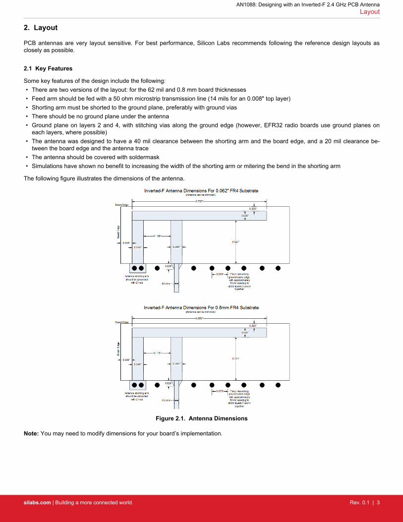
2. Layout
PCB antennas are very layout sensitive. For best performance, Silicon Labs recommends following the reference design layouts asclosely as possible.
2.1 Key Features
Some key features of the design include the following:• There are two versions of the layout: for the 62 mil and 0.8 mm board thicknesses• Feed arm should be fed with a 50 ohm microstrip transmission line (14 mils for an 0.008″ top layer)• Shorting arm must be shorted to the ground plane, preferably with ground vias• There should be no ground plane under the antenna• Ground plane on layers 2 and 4, with stitching vias along the ground edge (however, EFR32 radio boards use ground planes on
each layers, where possible)• The antenna was designed to have a 40 mil clearance between the shorting arm and the board edge, and a 20 mil clearance be-
tween the board edge and the antenna trace• The antenna should be covered with soldermask• Simulations have shown no benefit to increasing the width of the shorting arm or mitering the bend in the shorting arm
The following figure illustrates the dimensions of the antenna.
Figure 2.1. Antenna Dimensions
Note: You may need to modify dimensions for your board’s implementation.
AN1088: Designing with an Inverted-F 2.4 GHz PCB AntennaLayout
silabs.com | Building a more connected world. Rev. 0.1 | 3

2.1.1 Board Stackup
The following figure shows the board stackups used in the designs.
Figure 2.2. Board Stackup
AN1088: Designing with an Inverted-F 2.4 GHz PCB AntennaLayout
silabs.com | Building a more connected world. Rev. 0.1 | 4
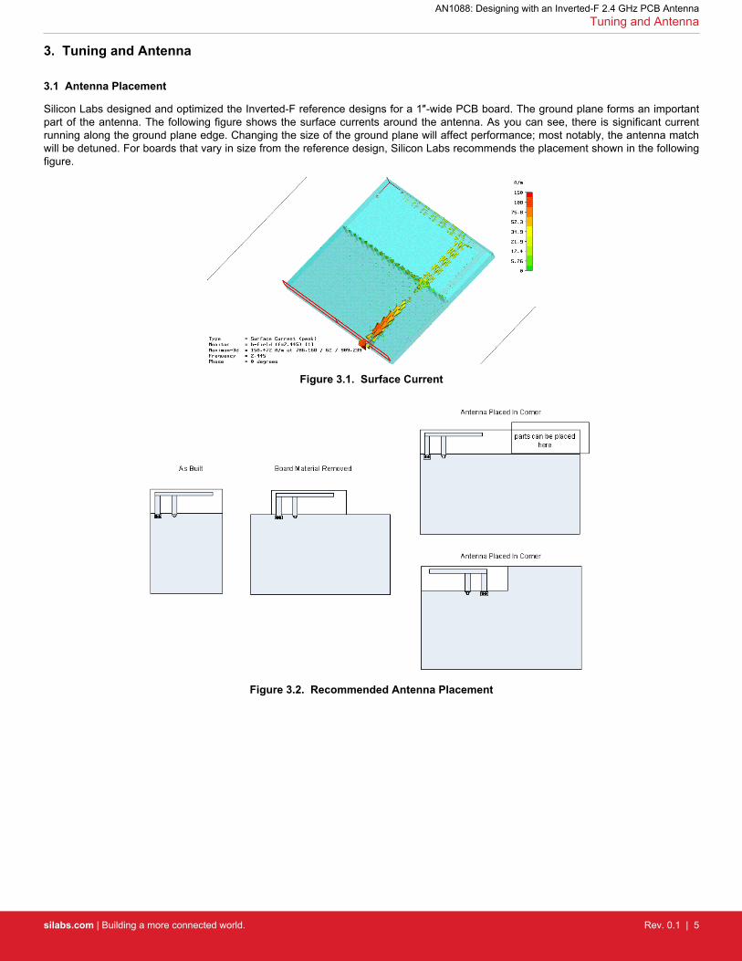
3. Tuning and Antenna
3.1 Antenna Placement
Silicon Labs designed and optimized the Inverted-F reference designs for a 1″-wide PCB board. The ground plane forms an importantpart of the antenna. The following figure shows the surface currents around the antenna. As you can see, there is significant currentrunning along the ground plane edge. Changing the size of the ground plane will affect performance; most notably, the antenna matchwill be detuned. For boards that vary in size from the reference design, Silicon Labs recommends the placement shown in the followingfigure.
Figure 3.1. Surface Current
Figure 3.2. Recommended Antenna Placement
AN1088: Designing with an Inverted-F 2.4 GHz PCB AntennaTuning and Antenna
silabs.com | Building a more connected world. Rev. 0.1 | 5

3.2 Tuning
Silicon Labs designed the printed antenna to provide a 50-Ohm output. An inverted-F antenna can inherently be matched to 50 ohmswithout using any external tuning component. However, board size, plastic enclosures, metal shielding, and components in close prox-imity to the antenna can affect antenna performance. For best performance, the antenna might require tuning that can be realized bytwo ways:• Dimension changes in the antenna layout structure, or• Applying external tuning components.
The latter is typically the preferred solution when layout modification is not required on a custom design. To accomplish this, SiliconLabs generally recommends reserving SMD placeholders for external antenna tuning components, where the suggested external an-tenna matching structure is a 3-element PI network. You can achieve a good match using a maximum of two elements (with one seriesand one shunt component) of the PI network. Any unknown passive impedance can get matched to 50 ohms on this PI network, sinceall L, C, L-C, C-L combinations can be realized on it and therefore any de-tuning effect can be compensated out.
The following figure shows the values of L required for the reference design prototypes. All four designs required C1/C2 to be unpopula-ted. Note that every implementation of the antenna design will require different combinations of inductors and capacitors. The EM2600.8mm reference design has the printed inverted-F antenna inherently matched to 50 ohms.
Figure 3.3. Antenna Matching Components
• EM250 62 mil: L = 2.0 nH• EM260 62 mil: L = 1.8 nH• EM250 0.8mm: L = 1.8 nH• EM260 0.8mm: L = 0 ohm• C1, C2 are not populated
AN1088: Designing with an Inverted-F 2.4 GHz PCB AntennaTuning and Antenna
silabs.com | Building a more connected world. Rev. 0.1 | 6

4. Antenna Performance
Silicon Labs designed the antennas using CST Microwave Studio. Antenna gain patterns for two board thicknesses were simulated; thefollowing two figures show this for the 62 mil thick board and for the 0.8 mm board, respectively. The gain shown is the absolute sum ofboth polarizations. These figures also show the board orientation.
Figure 4.1. Simulation of Gain Pattern for the 62 mil Antenna
AN1088: Designing with an Inverted-F 2.4 GHz PCB AntennaAntenna Performance
silabs.com | Building a more connected world. Rev. 0.1 | 7

Figure 4.2. Simulation of Gain Pattern for the 0.8 mm Antenna
AN1088: Designing with an Inverted-F 2.4 GHz PCB AntennaAntenna Performance
silabs.com | Building a more connected world. Rev. 0.1 | 8

4.1 Effects of Manufacturing Variations
Silicon Labs designed both antennas to have enough excess bandwidth to maintain performance over manufacturing tolerances. Thefollowing figure shows that a good match can still be maintained when varying the dielectric constant between 4.3 and 4.8 and theboard thickness by +/-3 mils.
Figure 4.3. Effects of Manufacturing Tolerances
4.2 Measured Antenna Patterns
Silicon Labs measured antenna patterns for eight prototype boards—two each of 62 mils and 0.8mm for both the EM250 and EM260—in a 5 meter anechoic chamber. Patterns in three orthogonal planes were measured for both polarizations. The following figures illus-trate these patterns for EM250 62 mil boards, EM260 62 mil boards, EM250 0.8 mm boards, and EM260 0.8 mm boards, respectively.
AN1088: Designing with an Inverted-F 2.4 GHz PCB AntennaAntenna Performance
silabs.com | Building a more connected world. Rev. 0.1 | 9

4.2.1 Antenna Patterns for EM250 62 mil Boards
SN01—EUT flat SN02—EUT flat
SN01—EUT side SN02—EUT side
SN01—EUT vertical SN02—EUT vertical
Figure 4.4. Measured Antenna Patterns for EM250 62 mil Boards
AN1088: Designing with an Inverted-F 2.4 GHz PCB AntennaAntenna Performance
silabs.com | Building a more connected world. Rev. 0.1 | 10

4.2.2 Antenna Patterns for EM260 62 mil Boards
SN01—EUT flat SN02—EUT flat
SN01—EUT side SN02—EUT side
SN01—EUT vertical SN02—EUT
Figure 4.5. Measured Antenna Patterns for EM260 62 mil Boards
AN1088: Designing with an Inverted-F 2.4 GHz PCB AntennaAntenna Performance
silabs.com | Building a more connected world. Rev. 0.1 | 11

4.2.3 Antenna Patterns for EM250 0.8 mm Boards
SN01—EUT flat SN02—EUT flat
SN01—EUT side SN02—EUT side
SN01—EUT vertical SN02—EUT vertical
Figure 4.6. Measured Antenna Patterns for EM250 0.8 mm Boards
AN1088: Designing with an Inverted-F 2.4 GHz PCB AntennaAntenna Performance
silabs.com | Building a more connected world. Rev. 0.1 | 12

4.2.4 Antenna Patterns for EM260 0.8 mm Boards
SN01—EUT flat SN02—EUT flat
SN01—EUT side SN02—EUT side
SN01—EUT vertical SN02—EUT vertical
Figure 4.7. Measured Antenna Patterns for EM260 0.8 mm Boards
AN1088: Designing with an Inverted-F 2.4 GHz PCB AntennaAntenna Performance
silabs.com | Building a more connected world. Rev. 0.1 | 13

5. After Reading this Document
If you have questions about the information described in this document, please contact support at https://www.silabs.com/support.
AN1088: Designing with an Inverted-F 2.4 GHz PCB AntennaAfter Reading this Document
silabs.com | Building a more connected world. Rev. 0.1 | 14

http://www.silabs.com
Silicon Laboratories Inc.400 West Cesar ChavezAustin, TX 78701USA
Smart. Connected. Energy-Friendly.
Productswww.silabs.com/products
Qualitywww.silabs.com/quality
Support and Communitycommunity.silabs.com
DisclaimerSilicon Labs intends to provide customers with the latest, accurate, and in-depth documentation of all peripherals and modules available for system and software implementers using or intending to use the Silicon Labs products. Characterization data, available modules and peripherals, memory sizes and memory addresses refer to each specific device, and "Typical" parameters provided can and do vary in different applications. Application examples described herein are for illustrative purposes only. Silicon Labs reserves the right to make changes without further notice and limitation to product information, specifications, and descriptions herein, and does not give warranties as to the accuracy or completeness of the included information. Silicon Labs shall have no liability for the consequences of use of the information supplied herein. This document does not imply or express copyright licenses granted hereunder to design or fabricate any integrated circuits. The products are not designed or authorized to be used within any Life Support System without the specific written consent of Silicon Labs. A "Life Support System" is any product or system intended to support or sustain life and/or health, which, if it fails, can be reasonably expected to result in significant personal injury or death. Silicon Labs products are not designed or authorized for military applications. Silicon Labs products shall under no circumstances be used in weapons of mass destruction including (but not limited to) nuclear, biological or chemical weapons, or missiles capable of delivering such weapons.
Trademark InformationSilicon Laboratories Inc.® , Silicon Laboratories®, Silicon Labs®, SiLabs® and the Silicon Labs logo®, Bluegiga®, Bluegiga Logo®, Clockbuilder®, CMEMS®, DSPLL®, EFM®, EFM32®, EFR, Ember®, Energy Micro, Energy Micro logo and combinations thereof, "the world’s most energy friendly microcontrollers", Ember®, EZLink®, EZRadio®, EZRadioPRO®, Gecko®, ISOmodem®, Micrium, Precision32®, ProSLIC®, Simplicity Studio®, SiPHY®, Telegesis, the Telegesis Logo®, USBXpress®, Zentri and others are trademarks or registered trademarks of Silicon Labs. ARM, CORTEX, Cortex-M3 and THUMB are trademarks or registered trademarks of ARM Holdings. Keil is a registered trademark of ARM Limited. All other products or brand names mentioned herein are trademarks of their respective holders.


![STUDY | PCB DIMENSION (Length) Attracting Tomorrow...Product Marketing [Jan 2018] 6 Attracting Tomorrow ANTENNA DESIGN APPLICATION NOTES Frequency (GHz) SIMULATION STUDY | MATCHING](https://static.fdocuments.us/doc/165x107/60f8523348769205e6696631/study-pcb-dimension-length-attracting-tomorrow-product-marketing-jan-2018.jpg)


