
23: ' # '8& *#2 & 9 - InTech - Opencdn.intechopen.com/pdfs-wm/9966.pdf ·...
15
3,350+ OPEN ACCESS BOOKS 108,000+ INTERNATIONAL AUTHORS AND EDITORS 115+ MILLION DOWNLOADS BOOKS DELIVERED TO 151 COUNTRIES AUTHORS AMONG TOP 1% MOST CITED SCIENTIST 12.2% AUTHORS AND EDITORS FROM TOP 500 UNIVERSITIES Selection of our books indexed in the Book Citation Index in Web of Science™ Core Collection (BKCI) Chapter from the book Advanced Microwave and Millimeter Wave Technologies Semiconductor Devices Circuits and Systems Downloaded from: http://www.intechopen.com/books/advanced-microwave-and- millimeter-wave-technologies-semiconductor-devices-circuits-and-systems PUBLISHED BY World's largest Science, Technology & Medicine Open Access book publisher Interested in publishing with IntechOpen? Contact us at [email protected]
Transcript of 23: ' # '8& *#2 & 9 - InTech - Opencdn.intechopen.com/pdfs-wm/9966.pdf ·...

3,350+OPEN ACCESS BOOKS
108,000+INTERNATIONAL
AUTHORS AND EDITORS115+ MILLION
DOWNLOADS
BOOKSDELIVERED TO
151 COUNTRIES
AUTHORS AMONG
TOP 1%MOST CITED SCIENTIST
12.2%AUTHORS AND EDITORS
FROM TOP 500 UNIVERSITIES
Selection of our books indexed in theBook Citation Index in Web of Science™
Core Collection (BKCI)
Chapter from the book Advanced Microwave and Millimeter Wave TechnologiesSemiconductor Devices Circuits and SystemsDownloaded from: http://www.intechopen.com/books/advanced-microwave-and-millimeter-wave-technologies-semiconductor-devices-circuits-and-systems
PUBLISHED BY
World's largest Science,Technology & Medicine
Open Access book publisher
Interested in publishing with IntechOpen?Contact us at [email protected]

The present and future trends in High Power Microwave and Millimeter Wave Technologies 1
The present and future trends in High Power Microwave and Millimeter Wave Technologies
S. Azam and Q. Wahab
X
The present and future trends in High Power Microwave and Millimeter Wave Technologies
S. Azam1, 3 and Q. Wahab1, 2, 4
1) Department of Physics (IFM), Linköping University, SE-581 83, Linköping, Sweden 2) Swedish Defense Research Agency (FOI), SE-581 11, Linköping, Sweden
3) Department of Electrical Engineering, Linköping University, SE-581 83, Linköping, Sweden
4) Department of Electronic Engineering, ECE Faculty, NED University of Engineering and Technology, 75270 Karachi, Pakistan
1. Introduction
Microwave and millimeter wave high-power vacuum electron devices (VEDs) are essential elements in specialized military, scientific, medical and space applications. They can produce mega watts of power which would be equal to the power of thousands of solid state power devices (SSPDs). Similarly, in most of today's T/R-Modules of active phased array antennas for radars and electronic warfare applications GaAs based hybrid and MMIC amplifiers are used. The early applications of millimeter-wave MMICs were in military, space and astronomy systems. They are now also utilized for civil applications, such as communications and automotive radars. As transmission speeds in next-generation wireless communications have become faster, wireless base stations that operate in the microwave frequency range consume an ever-increasing amount of power. The mm waves (above 30 GHz) deliver high speed and good directionality and have a large amount of available bandwidth that is currently not being used. They have the potential for use in high-speed transmissions. Point-to-point wireless is a key market for growth since it can replace fiber-optic cable in areas where fiber is too difficult or costly to install. But the real high volume action at mm-wave will likely be in the MMICs for automobile radar systems devices for short-range radar (24 GHz) and long-range radar (77 GHz). Such radars will not only be used for collision avoidance and warning, but also for side- and rear-looking sensors for lane changing, backup warning and parking assistance. While only available in high-end automobiles at present, cost reductions in MMIC chip manufacturing could lead to significant deployment in all cars in the future. SiC MESFETs and GaN HEMTs have wide bandgap features of high electric breakdown field strength, high electron saturation velocity and high operating temperature. The high power density combined with the comparably high impedance attainable by these devices also offers new possibilities for wideband power microwave systems. The SiC MESFETs has high cost and frequency limitation of X band. On the other hand the GaN transistors have the potential to disrupt at least part of the very large VEDs market and could replace at least
1
www.intechopen.com

Advanced Microwave and Millimeter Wave Technologies: Semiconductor Devices, Circuits and Systems2
some microwave and millimeter wave VEDs. The hybrid and MMIC amplifiers based on AlGaN/GaN technology has demonstrated higher output power levels, broader bandwidth, increased power added efficiency and higher operating voltages compare to GaAs for performance improvement to meet future requirements. Very promising results up to 35 GHz are demonstrated by GaN HEMT technology [1]-[8]. Resulting power density is about ten times higher than that demonstrated in GaAs. To make GaN cost competitive with other technologies, Nitronex Corp has developed GaN transistors on low-cost 100 mm silicon substrates (GaN-on-silicon growth technology). These transistors are commercially available which cover cellular phones, wireless LANs and other applications at the lower end of the microwave frequency spectrum (1-5 GHz). The devices for high frequencies and powers are in progress. This is believed to have a major impact in the future development of millimeter-wave systems. Since low-cost mass-production potential pushes forward the technology, a very high integration of circuit functions on a single chip is possible. Si-based other solid-state transistor amplifiers are typically fabricated using a combination of silicon bipolar and laterally diffused metal oxide semiconductor (LDMOS) technologies. LDMOS technology works well in UHF and VHF frequencies up to around 3.5 GHz. Typical power levels for these devices are usually in the <200 W range; however multi-die modules can offer power levels up to 1000 W [9]. Although LDMOS transistors are also low cost but they have the power handling and frequency limitations.
2. Classification of Power Devices
RF power devices can be broadly classified into three families:
2.1 Electron beam devices (EBD) Travelling-wave tubes (TWTs), klystrons and the inductive output tubes (“IOTs”) all belong to the EBD family. They all require multiple operating voltages, one of which is a high DC voltage (tens of kV) that accelerates the electron beam. The TWTs are presently produced for all common microwave communication and radar bands. It has been recently shown that it is feasible to build an active 2-D phased array at X-band using TWTs that fit within the array lattice, one TWT per element [10]. The DC-to-RF conversion efficiency is poor, 25-35 %, implying severely increased operating costs compared to other devices. The Klystrons has very high output power per device. At 30 – 2000 kW per device, the output power is 30…1000 times greater than that needed to drive an individual array element, thus requiring a very complicated system of power dividers and high-power phase-shifters to distribute and control the power flow to as many as 1000 elements per klystron. In a feed system of this kind, variable power tapering is almost impossible to realize. Also a single failed device will result in a large fraction of the array losing power at once. Also, the instantaneous power bandwidth of a large klystrons is only marginally sufficient, or even insufficient, to meet the range resolution requirement. The IOTs also has output power levels in the 30 – 70 kilowatt range and are subject to the same complications as the klystrons with regard to the RF power distribution / feed / beam-steering system.
2.2 Power grid tubes (PGTs) These tubes come in many shapes and sizes. There should be no problem finding a tube in the power range of one-kilowatt. A kilowatt is in the right power range for feeding an individual phased-array element, so tubes of this class could be used as the active elements of element-level power amplifiers. However, power grid tubes need multiple operating voltages, one of which is always a medium high DC voltage (> 2 kV), thus necessitating a fairly complicated power supply system, relatively short lifetimes and the more long-lived directly heated filament cathode types instead consume substantial amounts of filament-heating power, which reduces the overall DC-to-RF conversion efficiency significantly.
2.3 Solid-state Semiconductor Power Devices (SSPDs) The maximum output power that can be obtained from an RF power transistor is limited by the physical properties of the semiconductor material, in particular the safe junction/channel power density. Increasing the junction/channel area and reducing the device thickness in an attempt to increase power also increases the junction/gate capacitance, consequently reducing frequency and power gain. The heat resistance between the semi-conductor die and the heat sink determines how much dissipated power can be transported away from the die at the maximum allowed device temperature and is often the factor that the ultimately limits the output power. Until recently, these factors combined to limit the practical output power of CW-rated semiconductor devices to about 150 watts at all frequencies from VHF upwards. But during the last decade, demands from industry for better devices for the base stations for 3rd generation mobile telephone systems have generated much R&D to push the upper frequency power limit to 100 Watt and even higher. When operated within their ratings, RF power semiconductors show excellent lifetimes, upwards of many tens of thousands of hours, primarily limited by slow electro-migration of the metal used in contact pads and bonds. Semiconductor devices often operated by a single power supply in the 28 – 50 volt range, thus simplifying the power supply problem dramatically as compared to all electron devices. An additional advantage of FETs is that, being majority carrier devices, they do not suffer from thermal runaway effects. Biasing is also very simple, requiring only a source of adjustable positive voltage; the bias voltage can be derived from the main power supply through a voltage divider or a small regulator IC. A comparison of these devices on the basis of device characteristics is given in Table 1.
Device Type Pmax
(kW)
Drain Eff.
%
Gain
(dB)
Operating
voltage (kV)
Life time
(hours)
SSPDs 0.5 50-65 10-17 0.025-0.1 50x103
PGTs 0.5-10 50-60 10-13 0.5-10 (3-10)x103
EBDs 0.1-2000 25-60 20-40 25-100 (10-20)x103
Table 1. Comparison of power devices
www.intechopen.com

The present and future trends in High Power Microwave and Millimeter Wave Technologies 3
some microwave and millimeter wave VEDs. The hybrid and MMIC amplifiers based on AlGaN/GaN technology has demonstrated higher output power levels, broader bandwidth, increased power added efficiency and higher operating voltages compare to GaAs for performance improvement to meet future requirements. Very promising results up to 35 GHz are demonstrated by GaN HEMT technology [1]-[8]. Resulting power density is about ten times higher than that demonstrated in GaAs. To make GaN cost competitive with other technologies, Nitronex Corp has developed GaN transistors on low-cost 100 mm silicon substrates (GaN-on-silicon growth technology). These transistors are commercially available which cover cellular phones, wireless LANs and other applications at the lower end of the microwave frequency spectrum (1-5 GHz). The devices for high frequencies and powers are in progress. This is believed to have a major impact in the future development of millimeter-wave systems. Since low-cost mass-production potential pushes forward the technology, a very high integration of circuit functions on a single chip is possible. Si-based other solid-state transistor amplifiers are typically fabricated using a combination of silicon bipolar and laterally diffused metal oxide semiconductor (LDMOS) technologies. LDMOS technology works well in UHF and VHF frequencies up to around 3.5 GHz. Typical power levels for these devices are usually in the <200 W range; however multi-die modules can offer power levels up to 1000 W [9]. Although LDMOS transistors are also low cost but they have the power handling and frequency limitations.
2. Classification of Power Devices
RF power devices can be broadly classified into three families:
2.1 Electron beam devices (EBD) Travelling-wave tubes (TWTs), klystrons and the inductive output tubes (“IOTs”) all belong to the EBD family. They all require multiple operating voltages, one of which is a high DC voltage (tens of kV) that accelerates the electron beam. The TWTs are presently produced for all common microwave communication and radar bands. It has been recently shown that it is feasible to build an active 2-D phased array at X-band using TWTs that fit within the array lattice, one TWT per element [10]. The DC-to-RF conversion efficiency is poor, 25-35 %, implying severely increased operating costs compared to other devices. The Klystrons has very high output power per device. At 30 – 2000 kW per device, the output power is 30…1000 times greater than that needed to drive an individual array element, thus requiring a very complicated system of power dividers and high-power phase-shifters to distribute and control the power flow to as many as 1000 elements per klystron. In a feed system of this kind, variable power tapering is almost impossible to realize. Also a single failed device will result in a large fraction of the array losing power at once. Also, the instantaneous power bandwidth of a large klystrons is only marginally sufficient, or even insufficient, to meet the range resolution requirement. The IOTs also has output power levels in the 30 – 70 kilowatt range and are subject to the same complications as the klystrons with regard to the RF power distribution / feed / beam-steering system.
2.2 Power grid tubes (PGTs) These tubes come in many shapes and sizes. There should be no problem finding a tube in the power range of one-kilowatt. A kilowatt is in the right power range for feeding an individual phased-array element, so tubes of this class could be used as the active elements of element-level power amplifiers. However, power grid tubes need multiple operating voltages, one of which is always a medium high DC voltage (> 2 kV), thus necessitating a fairly complicated power supply system, relatively short lifetimes and the more long-lived directly heated filament cathode types instead consume substantial amounts of filament-heating power, which reduces the overall DC-to-RF conversion efficiency significantly.
2.3 Solid-state Semiconductor Power Devices (SSPDs) The maximum output power that can be obtained from an RF power transistor is limited by the physical properties of the semiconductor material, in particular the safe junction/channel power density. Increasing the junction/channel area and reducing the device thickness in an attempt to increase power also increases the junction/gate capacitance, consequently reducing frequency and power gain. The heat resistance between the semi-conductor die and the heat sink determines how much dissipated power can be transported away from the die at the maximum allowed device temperature and is often the factor that the ultimately limits the output power. Until recently, these factors combined to limit the practical output power of CW-rated semiconductor devices to about 150 watts at all frequencies from VHF upwards. But during the last decade, demands from industry for better devices for the base stations for 3rd generation mobile telephone systems have generated much R&D to push the upper frequency power limit to 100 Watt and even higher. When operated within their ratings, RF power semiconductors show excellent lifetimes, upwards of many tens of thousands of hours, primarily limited by slow electro-migration of the metal used in contact pads and bonds. Semiconductor devices often operated by a single power supply in the 28 – 50 volt range, thus simplifying the power supply problem dramatically as compared to all electron devices. An additional advantage of FETs is that, being majority carrier devices, they do not suffer from thermal runaway effects. Biasing is also very simple, requiring only a source of adjustable positive voltage; the bias voltage can be derived from the main power supply through a voltage divider or a small regulator IC. A comparison of these devices on the basis of device characteristics is given in Table 1.
Device Type Pmax
(kW)
Drain Eff.
%
Gain
(dB)
Operating
voltage (kV)
Life time
(hours)
SSPDs 0.5 50-65 10-17 0.025-0.1 50x103
PGTs 0.5-10 50-60 10-13 0.5-10 (3-10)x103
EBDs 0.1-2000 25-60 20-40 25-100 (10-20)x103
Table 1. Comparison of power devices
www.intechopen.com

Advanced Microwave and Millimeter Wave Technologies: Semiconductor Devices, Circuits and Systems4
3. VEDs vs SSPDs
Following are the main fundamental physical differences in SSPDs and VEDs; 1: In vacuum microwave electronic devices the electron stream moves without
collision through an evacuated region between anode and cathode. As electrons pass without any collision, there is no loss in their energy (hence less efficiency loss) and thus no heat is generated during electron current flow through the device. The only heat is produced in the collector of VEDs, due to that energy of electrons which is not converted into microwaves. In SSPDs, the electron current drifts between Emitter/Source and collector/Drain through a solid material and experience collisions. The electrons current waste some of its KE inside the device. Thus these devices have lower electron mobility compare to vacuum devices, which is an advantage for VEDs in terms of high power at high frequencies.
2: At long term high operating temperatures the performance of the device is degraded specially mobility is reduced which reduces performance at high frequencies. To keep the active region temperature of a microwave power transistor at acceptable low levels, the solid state devices need larger heat sink compare to VEDs, because the interaction region in VEDs is surrounded by Vacuum. For this purpose the base plate for solid state devices must be kept at or below 30 C, while VEDs can operate with base plate temperatures of 250 C.
3: In solid state devices the long term ionizing radiations must be avoided to prevent device degradation, while VEDs are virtually immune to ionizing radiation fluxes which make them suitable choice for the applications in space.
4: The VEDs have high electric field and power densities compare to solid state devices.
5: The SSPDs are smaller in size and low cost compare to VEDs. 6: The SSPDs are easy to fabricate compare to VEDs.
4. Why GaN transistors but not GaAs?
GaAs-based amplifiers are well-known devices currently used as pre-driver, driver, and even final-stage amplifiers for radar applications. GaN transistors and MMICs challenge GaAs technology mostly in high-bandwidth, high power applications, because, due to the smaller required device periphery for a given specified output power, good impedance matching can be achieved for GaN FETs over a broader frequency range than for GaAs pHEMTs. Also, Practical manufacturing of much higher power GaAs FETs than those currently available is facing significant technical difficulties. The wide bandgap of GaN increases the breakdown field by five times and the power density by a factor of 10 to 20, compared with GaAs-based devices. The GaN components are therefore smaller and have a lower capacitance for the same operating power, which means that amplifiers can operate over a wider bandwidth while exhibiting good input and output matching. GaN devices are also highly efficient because they can operate at higher voltages (24–35 V, compared with 5–8 V for GaAs-based devices at millimeter-wave frequencies), as well as having a lower on resistance. The high voltage also improves the power supply efficiency,
while the two dimensional electron gas (2DEG) produces a high electron velocity, ensuring good signal gain at K, Q and even W band frequencies. The unique attribute of the AlGaN/GaN structure is the possibility of building high channel charge, which increases the device’s current handling capability. Because GaN is a strongly polar material, the strain resulting from growing lattice-mismatched AlGaN on GaN induces a piezoelectric charge. This supplies additional electrons to the HEMT channel. This total channel charge is roughly four to five times higher than for AlGaAs/GaAs HEMTs. This piezoelectric property is a unique power-boosting bonus factor for AlGaN/GaN HEMTs. GaN devices built on SiC substrates have a thermal conductivity 10 times higher than those fabricated using GaAs, which means that these wide bandgap devices can operate at higher power densities. GaN HEMTs can also work at higher temperatures, which reduce the need for cooling and allows for a more compact module design. The comparison in GaAs and GaN on the basis of parameters required for high power performance is summarized in Table 2. The introduction of GaN on Silicon (most highly refined semiconductor substrates in the world are silicon wafers) is another great advantage in terms of cost. High volume production is possible because of growth on large silicon substrate. This GaN-on-silicon approach yields a low-cost, high-performance platform for high-frequency, high-power products, which is a potentially exciting combination. The most important is the process similarities of HEMT in both technologies; hence GaN HEMT can share production process with GaAs HEMT.
Parameter GaAs GaN
Maximum Operating Voltage
(Volts)
20 48
Maximum Current (mA) 500 ~1000
Maximum Breakdown Voltage
(Volts)
40 >100
Maximum Power Density (W/mm) 1.5 >8
Table 2. Comparison of GaN and GaAs
5. New Developments in GaN Technology
In only 16 years (since 1993), GaN-based transistors have evolved tremendously from a poor initial performance [11] to worldwide commercialization as power amplifiers in the S and X bands [12]. To increase their frequency of operation to millimeter and sub millimeter wave frequencies, improved growth in combination with the introduction of new device structures [13]-[15] have been reported. These new structures have allowed devices with a current gain cutoff frequency fT in excess of 150 GHz and a maximum oscillation frequency
www.intechopen.com

The present and future trends in High Power Microwave and Millimeter Wave Technologies 5
3. VEDs vs SSPDs
Following are the main fundamental physical differences in SSPDs and VEDs; 1: In vacuum microwave electronic devices the electron stream moves without
collision through an evacuated region between anode and cathode. As electrons pass without any collision, there is no loss in their energy (hence less efficiency loss) and thus no heat is generated during electron current flow through the device. The only heat is produced in the collector of VEDs, due to that energy of electrons which is not converted into microwaves. In SSPDs, the electron current drifts between Emitter/Source and collector/Drain through a solid material and experience collisions. The electrons current waste some of its KE inside the device. Thus these devices have lower electron mobility compare to vacuum devices, which is an advantage for VEDs in terms of high power at high frequencies.
2: At long term high operating temperatures the performance of the device is degraded specially mobility is reduced which reduces performance at high frequencies. To keep the active region temperature of a microwave power transistor at acceptable low levels, the solid state devices need larger heat sink compare to VEDs, because the interaction region in VEDs is surrounded by Vacuum. For this purpose the base plate for solid state devices must be kept at or below 30 C, while VEDs can operate with base plate temperatures of 250 C.
3: In solid state devices the long term ionizing radiations must be avoided to prevent device degradation, while VEDs are virtually immune to ionizing radiation fluxes which make them suitable choice for the applications in space.
4: The VEDs have high electric field and power densities compare to solid state devices.
5: The SSPDs are smaller in size and low cost compare to VEDs. 6: The SSPDs are easy to fabricate compare to VEDs.
4. Why GaN transistors but not GaAs?
GaAs-based amplifiers are well-known devices currently used as pre-driver, driver, and even final-stage amplifiers for radar applications. GaN transistors and MMICs challenge GaAs technology mostly in high-bandwidth, high power applications, because, due to the smaller required device periphery for a given specified output power, good impedance matching can be achieved for GaN FETs over a broader frequency range than for GaAs pHEMTs. Also, Practical manufacturing of much higher power GaAs FETs than those currently available is facing significant technical difficulties. The wide bandgap of GaN increases the breakdown field by five times and the power density by a factor of 10 to 20, compared with GaAs-based devices. The GaN components are therefore smaller and have a lower capacitance for the same operating power, which means that amplifiers can operate over a wider bandwidth while exhibiting good input and output matching. GaN devices are also highly efficient because they can operate at higher voltages (24–35 V, compared with 5–8 V for GaAs-based devices at millimeter-wave frequencies), as well as having a lower on resistance. The high voltage also improves the power supply efficiency,
while the two dimensional electron gas (2DEG) produces a high electron velocity, ensuring good signal gain at K, Q and even W band frequencies. The unique attribute of the AlGaN/GaN structure is the possibility of building high channel charge, which increases the device’s current handling capability. Because GaN is a strongly polar material, the strain resulting from growing lattice-mismatched AlGaN on GaN induces a piezoelectric charge. This supplies additional electrons to the HEMT channel. This total channel charge is roughly four to five times higher than for AlGaAs/GaAs HEMTs. This piezoelectric property is a unique power-boosting bonus factor for AlGaN/GaN HEMTs. GaN devices built on SiC substrates have a thermal conductivity 10 times higher than those fabricated using GaAs, which means that these wide bandgap devices can operate at higher power densities. GaN HEMTs can also work at higher temperatures, which reduce the need for cooling and allows for a more compact module design. The comparison in GaAs and GaN on the basis of parameters required for high power performance is summarized in Table 2. The introduction of GaN on Silicon (most highly refined semiconductor substrates in the world are silicon wafers) is another great advantage in terms of cost. High volume production is possible because of growth on large silicon substrate. This GaN-on-silicon approach yields a low-cost, high-performance platform for high-frequency, high-power products, which is a potentially exciting combination. The most important is the process similarities of HEMT in both technologies; hence GaN HEMT can share production process with GaAs HEMT.
Parameter GaAs GaN
Maximum Operating Voltage
(Volts)
20 48
Maximum Current (mA) 500 ~1000
Maximum Breakdown Voltage
(Volts)
40 >100
Maximum Power Density (W/mm) 1.5 >8
Table 2. Comparison of GaN and GaAs
5. New Developments in GaN Technology
In only 16 years (since 1993), GaN-based transistors have evolved tremendously from a poor initial performance [11] to worldwide commercialization as power amplifiers in the S and X bands [12]. To increase their frequency of operation to millimeter and sub millimeter wave frequencies, improved growth in combination with the introduction of new device structures [13]-[15] have been reported. These new structures have allowed devices with a current gain cutoff frequency fT in excess of 150 GHz and a maximum oscillation frequency
www.intechopen.com
Advanced Microwave and Millimeter Wave Technologies: Semiconductor Devices, Circuits and Systems6
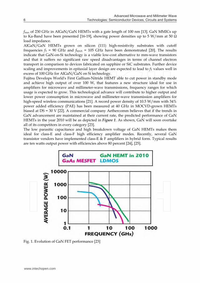
fmax of 230 GHz in AlGaN/GaN HEMTs with a gate length of 100 nm [13]. GaN MMICs up to Ka-Band have been presented [16-19], showing power densities up to 5 W/mm at 50 Ω load impedance. AlGaN/GaN HEMTs grown on silicon (111) high-resistivity substrates with cutoff frequencies fT = 90 GHz and fMAX = 105 GHz have been demonstrated [20]. The results indicate that GaN-on-Si technology is a viable low-cost alternative to mm-wave transistors and that it suffers no significant raw speed disadvantages in terms of channel electron transport in comparison to devices fabricated on sapphire or SiC substrates. Further device scaling and improvements in epitaxial layer design are expected to lead to fT values well in excess of 100 GHz for AlGaN/GaN on Si technology. Fujitsu Develops World's First Gallium-Nitride HEMT able to cut power in standby mode and achieve high output of over 100 W, that features a new structure ideal for use in amplifiers for microwave and millimeter-wave transmissions, frequency ranges for which usage is expected to grow. This technological advance will contribute to higher output and lower power consumption in microwave and millimeter-wave transmission amplifiers for high-speed wireless communications [21]. A record power density of 10.5 W/mm with 34% power added efficiency (PAE) has been measured at 40 GHz in MOCVD-grown HEMTs biased at DS = 30 V [22]. A commercial company Aethercomm believes that if the trends in GaN advancement are maintained at their current rate, the predicted performance of GaN HEMTs in the year 2010 will be as depicted in Figure 1. As shown, GaN will soon overtake all of its competitors in every category [23]. The low parasitic capacitance and high breakdown voltage of GaN HEMTs makes them ideal for class-E and class-F high efficiency amplifier modes. Recently, several GaN transistor vendors have implemented class-E & F amplifiers in hybrid form. Typical results are ten watts output power with efficiencies above 80 percent [24], [25].
Fig. 1. Evolution of GaN FET performance [23]
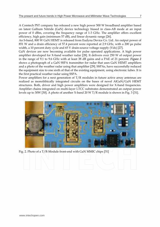
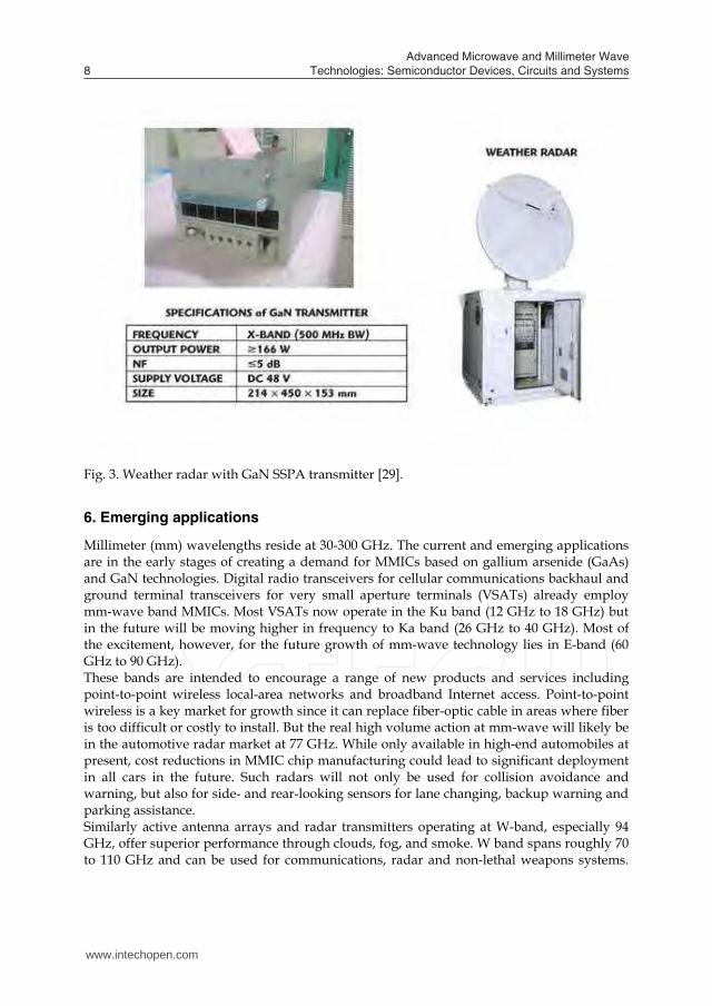
A Comtech PST company has released a new high power 500 W broadband amplifier based on latest Gallium Nitride (GaN) device technology biased in class-AB mode at an input power of 0 dBm, covering the frequency range of 1-3 GHz. The amplifier offers excellent efficiency, high gain (minimum 57 dB), and linear dynamic range [26]. An S-band, 800 W GaN HEMT is released from Eudyna Device Co. Ltd. An output power of 851 W and a drain efficiency of 57.4 percent were reported at 2.9 GHz, with a 200 μs pulse width, a 10 percent duty cycle and 65 V drain-source voltage supply (Vds) [27]. GaN devices are now becoming available for pulse operated applications. A high power amplifier developed for X-band weather radar [28]. It delivers over 250 W of output power in the range of 9.1 to 9.6 GHz with at least 38 dB gains and a PAE of 21 percent. Figure 2 shows a photograph of a GaN SSPA transmitter for radar that uses GaN HEMT amplifiers and a photo of the weather radar using that amplifier [29]. SSPAs, have successfully reduced the equipment size to one sixth of that of the existing equipment, using electronic tubes. It is the first practical weather radar using SSPA. Power amplifiers for a next generation of T/R modules in future active array antennas are realized as monolithically integrated circuits on the bases of novel AlGaN/GaN HEMT structures. Both, driver and high power amplifiers were designed for X-band frequencies. Amplifier chains integrated on multi-layer LTCC substrates demonstrated an output power levels up to 30W [30]. A photo of another X-band 20 W T/R module is shown in Fig. 3 [31].
Fig. 2. Photo of a T/R-Module front-end with GaN MMIC chips [31]
www.intechopen.com
The present and future trends in High Power Microwave and Millimeter Wave Technologies 7
fmax of 230 GHz in AlGaN/GaN HEMTs with a gate length of 100 nm [13]. GaN MMICs up to Ka-Band have been presented [16-19], showing power densities up to 5 W/mm at 50 Ω load impedance. AlGaN/GaN HEMTs grown on silicon (111) high-resistivity substrates with cutoff frequencies fT = 90 GHz and fMAX = 105 GHz have been demonstrated [20]. The results indicate that GaN-on-Si technology is a viable low-cost alternative to mm-wave transistors and that it suffers no significant raw speed disadvantages in terms of channel electron transport in comparison to devices fabricated on sapphire or SiC substrates. Further device scaling and improvements in epitaxial layer design are expected to lead to fT values well in excess of 100 GHz for AlGaN/GaN on Si technology. Fujitsu Develops World's First Gallium-Nitride HEMT able to cut power in standby mode and achieve high output of over 100 W, that features a new structure ideal for use in amplifiers for microwave and millimeter-wave transmissions, frequency ranges for which usage is expected to grow. This technological advance will contribute to higher output and lower power consumption in microwave and millimeter-wave transmission amplifiers for high-speed wireless communications [21]. A record power density of 10.5 W/mm with 34% power added efficiency (PAE) has been measured at 40 GHz in MOCVD-grown HEMTs biased at DS = 30 V [22]. A commercial company Aethercomm believes that if the trends in GaN advancement are maintained at their current rate, the predicted performance of GaN HEMTs in the year 2010 will be as depicted in Figure 1. As shown, GaN will soon overtake all of its competitors in every category [23]. The low parasitic capacitance and high breakdown voltage of GaN HEMTs makes them ideal for class-E and class-F high efficiency amplifier modes. Recently, several GaN transistor vendors have implemented class-E & F amplifiers in hybrid form. Typical results are ten watts output power with efficiencies above 80 percent [24], [25].
Fig. 1. Evolution of GaN FET performance [23]
A Comtech PST company has released a new high power 500 W broadband amplifier based on latest Gallium Nitride (GaN) device technology biased in class-AB mode at an input power of 0 dBm, covering the frequency range of 1-3 GHz. The amplifier offers excellent efficiency, high gain (minimum 57 dB), and linear dynamic range [26]. An S-band, 800 W GaN HEMT is released from Eudyna Device Co. Ltd. An output power of 851 W and a drain efficiency of 57.4 percent were reported at 2.9 GHz, with a 200 μs pulse width, a 10 percent duty cycle and 65 V drain-source voltage supply (Vds) [27]. GaN devices are now becoming available for pulse operated applications. A high power amplifier developed for X-band weather radar [28]. It delivers over 250 W of output power in the range of 9.1 to 9.6 GHz with at least 38 dB gains and a PAE of 21 percent. Figure 2 shows a photograph of a GaN SSPA transmitter for radar that uses GaN HEMT amplifiers and a photo of the weather radar using that amplifier [29]. SSPAs, have successfully reduced the equipment size to one sixth of that of the existing equipment, using electronic tubes. It is the first practical weather radar using SSPA. Power amplifiers for a next generation of T/R modules in future active array antennas are realized as monolithically integrated circuits on the bases of novel AlGaN/GaN HEMT structures. Both, driver and high power amplifiers were designed for X-band frequencies. Amplifier chains integrated on multi-layer LTCC substrates demonstrated an output power levels up to 30W [30]. A photo of another X-band 20 W T/R module is shown in Fig. 3 [31].
Fig. 2. Photo of a T/R-Module front-end with GaN MMIC chips [31]
www.intechopen.com
Advanced Microwave and Millimeter Wave Technologies: Semiconductor Devices, Circuits and Systems8
Fig. 3. Weather radar with GaN SSPA transmitter [29].
6. Emerging applications
Millimeter (mm) wavelengths reside at 30-300 GHz. The current and emerging applications are in the early stages of creating a demand for MMICs based on gallium arsenide (GaAs) and GaN technologies. Digital radio transceivers for cellular communications backhaul and ground terminal transceivers for very small aperture terminals (VSATs) already employ mm-wave band MMICs. Most VSATs now operate in the Ku band (12 GHz to 18 GHz) but in the future will be moving higher in frequency to Ka band (26 GHz to 40 GHz). Most of the excitement, however, for the future growth of mm-wave technology lies in E-band (60 GHz to 90 GHz). These bands are intended to encourage a range of new products and services including point-to-point wireless local-area networks and broadband Internet access. Point-to-point wireless is a key market for growth since it can replace fiber-optic cable in areas where fiber is too difficult or costly to install. But the real high volume action at mm-wave will likely be in the automotive radar market at 77 GHz. While only available in high-end automobiles at present, cost reductions in MMIC chip manufacturing could lead to significant deployment in all cars in the future. Such radars will not only be used for collision avoidance and warning, but also for side- and rear-looking sensors for lane changing, backup warning and parking assistance. Similarly active antenna arrays and radar transmitters operating at W-band, especially 94 GHz, offer superior performance through clouds, fog, and smoke. W band spans roughly 70 to 110 GHz and can be used for communications, radar and non-lethal weapons systems.
Novel wide bandgap RF circuit technology is sought for radar operation at W-band in brownout and degraded visibility conditions. This need has led to interest in the development of W-band high power, high efficiency amplifiers, which are currently realized almost exclusively in gallium arsenide (GaAs) and indium phosphide (InP) material systems due to their high transition frequency (Ft) performance [32], [33]. However, use of these devices has resulted in larger device peripheries for a given specified output power, more combining structures, higher combining losses, and lower power densities. These device technologies are not capable of meeting future peak power requirements. On the other hand, wide bandgap device technologies such as gallium nitride (GaN) can overcome these limitations as they can operate at higher voltages and have demonstrated power handling capabilities on the order 10 xs greater than that of GaAs or InP technologies. A three stage GaN MMIC power amplifiers for E-band radio applications is demonstrated that produce 500 mW of saturated output power in CW mode and have > 12 dB of associated power gain. The output power density from 300 μm output gate width GaN MMICs is seven times higher than the power density of commercially available GaAs pHEMT MMICs in this frequency range [34].
7. Millimeter band is not yet widely used. Why?
Due to faster transmission speeds in next-generation wireless communications, wireless base stations consume an ever-increasing amount of power. The millimeter wave frequency range above 30 GHz has a large amount of available bandwidth, because it delivers high speed and good directionality, its potential for use in high-speed transmissions is significant. However, due to millimeter-wave frequencies being higher than frequencies for conventional wireless transmissions, it has been difficult to develop amplifiers for practical use that are both compact and economical, and thus the millimeter band is not yet widely used.
8. CONCLUSIONS
Future Communication, EW and radar systems such as Base station, auto radars, the active phased-array radar (APAR) etc. will require increasingly smaller, more highly efficient SSPAs. In case of APAR, the desire for extremely fast scanning rates, much higher range, the ability to track and engage a tremendous number of targets, low probability of intercept and the ability to function as EW system, will require an innovative and cost-effective SSPD technology. The EBDs and PGTs are seen to be poor alternatives for the power amplifier of radars and other communication electronics in respect of power supply requirements, output power, bandwidth, fabrication and potential for graceful degradation compare to SSPDs especially PAs and MMICs based on wideband gap GaN technology transistors. Recent developments in the GaN HEMT have made it possible to realize highly efficient amplifiers at microwave frequencies. The results of GaN technology in terms of fT, fmax, power density, efficiency, band width etc. both at microwave and mm waves indicate that it will be the possible first choice for applications in future microwave and mm wave technologies.
www.intechopen.com
The present and future trends in High Power Microwave and Millimeter Wave Technologies 9
Fig. 3. Weather radar with GaN SSPA transmitter [29].
6. Emerging applications
Millimeter (mm) wavelengths reside at 30-300 GHz. The current and emerging applications are in the early stages of creating a demand for MMICs based on gallium arsenide (GaAs) and GaN technologies. Digital radio transceivers for cellular communications backhaul and ground terminal transceivers for very small aperture terminals (VSATs) already employ mm-wave band MMICs. Most VSATs now operate in the Ku band (12 GHz to 18 GHz) but in the future will be moving higher in frequency to Ka band (26 GHz to 40 GHz). Most of the excitement, however, for the future growth of mm-wave technology lies in E-band (60 GHz to 90 GHz). These bands are intended to encourage a range of new products and services including point-to-point wireless local-area networks and broadband Internet access. Point-to-point wireless is a key market for growth since it can replace fiber-optic cable in areas where fiber is too difficult or costly to install. But the real high volume action at mm-wave will likely be in the automotive radar market at 77 GHz. While only available in high-end automobiles at present, cost reductions in MMIC chip manufacturing could lead to significant deployment in all cars in the future. Such radars will not only be used for collision avoidance and warning, but also for side- and rear-looking sensors for lane changing, backup warning and parking assistance. Similarly active antenna arrays and radar transmitters operating at W-band, especially 94 GHz, offer superior performance through clouds, fog, and smoke. W band spans roughly 70 to 110 GHz and can be used for communications, radar and non-lethal weapons systems.
Novel wide bandgap RF circuit technology is sought for radar operation at W-band in brownout and degraded visibility conditions. This need has led to interest in the development of W-band high power, high efficiency amplifiers, which are currently realized almost exclusively in gallium arsenide (GaAs) and indium phosphide (InP) material systems due to their high transition frequency (Ft) performance [32], [33]. However, use of these devices has resulted in larger device peripheries for a given specified output power, more combining structures, higher combining losses, and lower power densities. These device technologies are not capable of meeting future peak power requirements. On the other hand, wide bandgap device technologies such as gallium nitride (GaN) can overcome these limitations as they can operate at higher voltages and have demonstrated power handling capabilities on the order 10 xs greater than that of GaAs or InP technologies. A three stage GaN MMIC power amplifiers for E-band radio applications is demonstrated that produce 500 mW of saturated output power in CW mode and have > 12 dB of associated power gain. The output power density from 300 μm output gate width GaN MMICs is seven times higher than the power density of commercially available GaAs pHEMT MMICs in this frequency range [34].
7. Millimeter band is not yet widely used. Why?
Due to faster transmission speeds in next-generation wireless communications, wireless base stations consume an ever-increasing amount of power. The millimeter wave frequency range above 30 GHz has a large amount of available bandwidth, because it delivers high speed and good directionality, its potential for use in high-speed transmissions is significant. However, due to millimeter-wave frequencies being higher than frequencies for conventional wireless transmissions, it has been difficult to develop amplifiers for practical use that are both compact and economical, and thus the millimeter band is not yet widely used.
8. CONCLUSIONS
Future Communication, EW and radar systems such as Base station, auto radars, the active phased-array radar (APAR) etc. will require increasingly smaller, more highly efficient SSPAs. In case of APAR, the desire for extremely fast scanning rates, much higher range, the ability to track and engage a tremendous number of targets, low probability of intercept and the ability to function as EW system, will require an innovative and cost-effective SSPD technology. The EBDs and PGTs are seen to be poor alternatives for the power amplifier of radars and other communication electronics in respect of power supply requirements, output power, bandwidth, fabrication and potential for graceful degradation compare to SSPDs especially PAs and MMICs based on wideband gap GaN technology transistors. Recent developments in the GaN HEMT have made it possible to realize highly efficient amplifiers at microwave frequencies. The results of GaN technology in terms of fT, fmax, power density, efficiency, band width etc. both at microwave and mm waves indicate that it will be the possible first choice for applications in future microwave and mm wave technologies.
www.intechopen.com
Advanced Microwave and Millimeter Wave Technologies: Semiconductor Devices, Circuits and Systems10
9. Acknowledgement The authors wish to acknowledge efforts of the Government of Oman for the financial support of this work and creating and financing the Sultan Qabos IT Chair at NED University of Engineering and Technology, Karachi, Pakistan.
10. References
[1] A. M. Darwish, K. Boutros, B. Luo, B. D. Huebschman, E. Viveiros, and H. A. Hung. Algan/gan ka-band 5-w mmic amplifier. IEEE Transactions on Microwave Theory and Techniques, 54(12):4456– 4463, 2006.
[2] K.S. Boutros, W.B. Luo, Y. Ma, G. Nagy, and J. Hacker. 5 W GaN mmic for millimeter-wave applications. IEEE Compound Semiconductor Integrated Circuit Symposium, 2006, pages 93–95, 2006.
[3] M. van Heijningen, F.E. van Vliet, R. Quay, F. van Raay, R. Kiefer, S. Muller, D. Krausse, M. Seelmann-Eggebert, M. Mikulla, and M. Schlechtweg. Ka-band algan/gan hemt high power and driver amplifier mmics. Gallium Arsenide and Other Semiconductor Application Symposium, 2005. EGAAS 2005. European, pages 237–240, 2005.
[4] Y.-F.Wu, A. Saxler, M. Moore, T.Wisleder, U.K. Mishra, and P. Parikh. “Field-plated gan hemts and amplifiers.” IEEE Compound Semiconductor Integrated Circuit Symposium (IEEE Cat. No.05CH37701), page 4, 2005.
[5] M. Nishijima, et al.; “A k-band algan/gan hfet mmic amplifier on sapphire using novel superlattice cap layer.” Microwave Symposium Digest, 2005 IEEE MTT-S International, 2005.
[6] M. Micovic, et al.; “Ka-band MMIC power amplifier in GaN HFET technology.“ Microwave Symposium Digest, 2004 IEEE MTT-S International, pages 3:1653–1656, 2004.
[7] Y.-F.Wu, M. Moore, A. Saxler, P. Smith, P.M. Chavarkar, and P. Parikh. 3.5-watt algan/gan hemts and amplifiers at 35 ghz. Electron Devices Meeting, 2003. IEDM ’03 Technical Digest. IEEE International, page 23.5.1, 2003.
[8] W.L. Pribble, J.W. Palmour, S.T. Sheppard, R.P. Smith, S.T. Allen, T.J. Smith, Z. Ring, J.J. Sumakeris, A.W. Saxler, and J.W. Milligan. Applications of sic mesfets and gan hemts in power amplifier design. Microwave Symposium Digest, 2002 IEEE MTT-S International, 3:1819–1822 vol.3, 2002.
[9] www.freescale.com/files/rf_if/doc/data_sheet/MRF6VP11KH.pdf [10] B. Levush and E.J. Dutkowski, “Vacuum Electronics: Status and Trends,” 2007 IEEE
Radar Conference, April 17–20, 2007, Boston, MA. [11] M. A. Khan, A. Bhattarai, J. N. Kuznia, and D. T. Olson, Appl. Phys. Lett. 63, 1214,
1993. [12] Cree, Inc., www.cree.com. [13] T. Palacios, A. Chakraborty, S. Heikman, S. Keller, S. P. DenBaars, and U. K.
Mishra, “AlGaN/GaN high electron mobility transistors with InGaN back-barrier,” IEEE Electron Device Lett., vol. 27, no. 1, pp. 13–15, Jan. 2006.
[14] M. Micovic, A. Kurdoghlian, P. Hashimoto, M. Hu, M. Antcliffe, P. J. Willadsen, W. S. Wong, R. Bowen, I. Milosavljevic, A. Schmitz, M. Wetzel, and D. H. Chow, BGaN HFET for W-band power applications,[ in IEEE International Electron Devices Meeting, 2006.
[15] M. Higashiwaki, T. Matsui, and T. Mimura, IEEE Electron Device Lett. 27, 16, 2006.[16] J.W. Palmour, J.W. Milligan, J. Henning, S.T. Allen, A. Ward, P. Parikh, R.P. Smith,
A. Saxler, M. Moore and Y. Wu, "SiC and GaN Based Transistor and Circuit Advances", Proc. GAAS 2004, Amsterdam, pp. 555–558.
[17] T. Inoue, Y. Ando, H. Miyamoto, Ta Nakayama, Y. Okamoto, K. Hataya and M. Kuzuhara, “30GHz-band 5.8 W High-Power AlGaN/GaN Heterojunction-FET”, MTTS 2004, Fort Worth, pp. 1649-1651.
[18] M. Micovic, Ara Kurdoghlian, H.P. Moyer, P. Hashimoto, A. Schmitz, I. Milosavljevic, P. J. Willadsen, W.-S. Wong, J. Duvall, M. Hu, M. J. Delaney, D. H. Chow, “Ka-band MMIC Power Amplifier in GaN HFET Technology”, MTT-S 2004, Fort Worth, pp. 1653-1656.
[19] Y.-F. Wu, M. Moore, A. Saxler, P. Smith, P.M. Chavarkar, P. Parikh, “3.5-Watt AlGaN/GaN HEMTs and Amplifiers at 35 GHz”, 2003 IEEE Int. Electron Device
Meeting.Dig., pp. 579-581, December 2003. [20] H.F. Sun, A.R. Alt, H. Benedickter and C.R. Bolognesi, “100 nm gate AlGaN/GaN
HEMTs on Silicon with fT = 90 GHz”, ELECTRONICS LETTERS 26th March 2009 Vol. 45 No. 7
[21] Fujitsu Limited and Fujitsu Laboratories Ltd. International Symposium on Compound Semiconductors (ISCS), held in Rust, Germany from September 21 – 24, 2008.
[22] T. Palacios, A. Chakraborty, S. Rajan, C. Poblenz, S. Keller, S. P. DenBaars, J. S. Speck, and U. K. Mishra, “High-Power AlGaN/GaN HEMTs for Ka-Band Applications”, IEEE ELECTRON DEVICE LETTERS, VOL. 26, NO. 11, pp. 781-783, NOVEMBER 2005
[23] http://www.mwjournal.com/search/article.asp?HH_ID=AR_5370,“Gallium Nitride Microwave Transistor Technology for Radar Applications”, Technical feature, Microwave Journal, Vol. 51 | No. 1 | January 2008 | Page 106
[24] Yong-Sub Lee *, Mun-Woo Lee, Yoon-Ha Jeong, "A 1-GHz GaN HEMT based class-E power amplifier with 80% efficiency" DOI 10.1002/mop.23803, 2008.
[25] David Schmelzer and Stephen I. Long, "A GaN HEMT Class F Amplifier at 2 GHz with > 80 % PAE" Compound Semiconductor Integrated Circuit Symposium, CSIC 2006. IEEE, pages: 96-99, 2006.
[26] http://www.comtechpst.com/products/specs/114.pdf [27] E. Mitani, et al, “An 800 W AlGaN/GaN HEMT for S-band High-power
Application,” 2009 CS Mantech Conference Digest, p. 213. [28] K. Kanto, et al, “An X-band 250 W Solid-state Power Amplifier Using GaN Power
HEMTs,” 2008 IEEE RWS Conference Digest, p. 77. [29] Toshiba Press Release, http://www.toshiba.co.jp/about/press/2009_11/
pr_j2801.htm. [30] Schuh, P. et al "Advanced High Power Amplifier Chain for X-Band T/R-Modules
based on GaN MMICs," The 1st European Microwave Integrated Circuits Conference, 2006. Page(s):241 - 244.
www.intechopen.com
The present and future trends in High Power Microwave and Millimeter Wave Technologies 11
9. Acknowledgement The authors wish to acknowledge efforts of the Government of Oman for the financial support of this work and creating and financing the Sultan Qabos IT Chair at NED University of Engineering and Technology, Karachi, Pakistan.
10. References
[1] A. M. Darwish, K. Boutros, B. Luo, B. D. Huebschman, E. Viveiros, and H. A. Hung. Algan/gan ka-band 5-w mmic amplifier. IEEE Transactions on Microwave Theory and Techniques, 54(12):4456– 4463, 2006.
[2] K.S. Boutros, W.B. Luo, Y. Ma, G. Nagy, and J. Hacker. 5 W GaN mmic for millimeter-wave applications. IEEE Compound Semiconductor Integrated Circuit Symposium, 2006, pages 93–95, 2006.
[3] M. van Heijningen, F.E. van Vliet, R. Quay, F. van Raay, R. Kiefer, S. Muller, D. Krausse, M. Seelmann-Eggebert, M. Mikulla, and M. Schlechtweg. Ka-band algan/gan hemt high power and driver amplifier mmics. Gallium Arsenide and Other Semiconductor Application Symposium, 2005. EGAAS 2005. European, pages 237–240, 2005.
[4] Y.-F.Wu, A. Saxler, M. Moore, T.Wisleder, U.K. Mishra, and P. Parikh. “Field-plated gan hemts and amplifiers.” IEEE Compound Semiconductor Integrated Circuit Symposium (IEEE Cat. No.05CH37701), page 4, 2005.
[5] M. Nishijima, et al.; “A k-band algan/gan hfet mmic amplifier on sapphire using novel superlattice cap layer.” Microwave Symposium Digest, 2005 IEEE MTT-S International, 2005.
[6] M. Micovic, et al.; “Ka-band MMIC power amplifier in GaN HFET technology.“ Microwave Symposium Digest, 2004 IEEE MTT-S International, pages 3:1653–1656, 2004.
[7] Y.-F.Wu, M. Moore, A. Saxler, P. Smith, P.M. Chavarkar, and P. Parikh. 3.5-watt algan/gan hemts and amplifiers at 35 ghz. Electron Devices Meeting, 2003. IEDM ’03 Technical Digest. IEEE International, page 23.5.1, 2003.
[8] W.L. Pribble, J.W. Palmour, S.T. Sheppard, R.P. Smith, S.T. Allen, T.J. Smith, Z. Ring, J.J. Sumakeris, A.W. Saxler, and J.W. Milligan. Applications of sic mesfets and gan hemts in power amplifier design. Microwave Symposium Digest, 2002 IEEE MTT-S International, 3:1819–1822 vol.3, 2002.
[9] www.freescale.com/files/rf_if/doc/data_sheet/MRF6VP11KH.pdf [10] B. Levush and E.J. Dutkowski, “Vacuum Electronics: Status and Trends,” 2007 IEEE
Radar Conference, April 17–20, 2007, Boston, MA. [11] M. A. Khan, A. Bhattarai, J. N. Kuznia, and D. T. Olson, Appl. Phys. Lett. 63, 1214,
1993. [12] Cree, Inc., www.cree.com. [13] T. Palacios, A. Chakraborty, S. Heikman, S. Keller, S. P. DenBaars, and U. K.
Mishra, “AlGaN/GaN high electron mobility transistors with InGaN back-barrier,” IEEE Electron Device Lett., vol. 27, no. 1, pp. 13–15, Jan. 2006.
[14] M. Micovic, A. Kurdoghlian, P. Hashimoto, M. Hu, M. Antcliffe, P. J. Willadsen, W. S. Wong, R. Bowen, I. Milosavljevic, A. Schmitz, M. Wetzel, and D. H. Chow, BGaN HFET for W-band power applications,[ in IEEE International Electron Devices Meeting, 2006.
[15] M. Higashiwaki, T. Matsui, and T. Mimura, IEEE Electron Device Lett. 27, 16, 2006.[16] J.W. Palmour, J.W. Milligan, J. Henning, S.T. Allen, A. Ward, P. Parikh, R.P. Smith,
A. Saxler, M. Moore and Y. Wu, "SiC and GaN Based Transistor and Circuit Advances", Proc. GAAS 2004, Amsterdam, pp. 555–558.
[17] T. Inoue, Y. Ando, H. Miyamoto, Ta Nakayama, Y. Okamoto, K. Hataya and M. Kuzuhara, “30GHz-band 5.8 W High-Power AlGaN/GaN Heterojunction-FET”, MTTS 2004, Fort Worth, pp. 1649-1651.
[18] M. Micovic, Ara Kurdoghlian, H.P. Moyer, P. Hashimoto, A. Schmitz, I. Milosavljevic, P. J. Willadsen, W.-S. Wong, J. Duvall, M. Hu, M. J. Delaney, D. H. Chow, “Ka-band MMIC Power Amplifier in GaN HFET Technology”, MTT-S 2004, Fort Worth, pp. 1653-1656.
[19] Y.-F. Wu, M. Moore, A. Saxler, P. Smith, P.M. Chavarkar, P. Parikh, “3.5-Watt AlGaN/GaN HEMTs and Amplifiers at 35 GHz”, 2003 IEEE Int. Electron Device
Meeting.Dig., pp. 579-581, December 2003. [20] H.F. Sun, A.R. Alt, H. Benedickter and C.R. Bolognesi, “100 nm gate AlGaN/GaN
HEMTs on Silicon with fT = 90 GHz”, ELECTRONICS LETTERS 26th March 2009 Vol. 45 No. 7
[21] Fujitsu Limited and Fujitsu Laboratories Ltd. International Symposium on Compound Semiconductors (ISCS), held in Rust, Germany from September 21 – 24, 2008.
[22] T. Palacios, A. Chakraborty, S. Rajan, C. Poblenz, S. Keller, S. P. DenBaars, J. S. Speck, and U. K. Mishra, “High-Power AlGaN/GaN HEMTs for Ka-Band Applications”, IEEE ELECTRON DEVICE LETTERS, VOL. 26, NO. 11, pp. 781-783, NOVEMBER 2005
[23] http://www.mwjournal.com/search/article.asp?HH_ID=AR_5370,“Gallium Nitride Microwave Transistor Technology for Radar Applications”, Technical feature, Microwave Journal, Vol. 51 | No. 1 | January 2008 | Page 106
[24] Yong-Sub Lee *, Mun-Woo Lee, Yoon-Ha Jeong, "A 1-GHz GaN HEMT based class-E power amplifier with 80% efficiency" DOI 10.1002/mop.23803, 2008.
[25] David Schmelzer and Stephen I. Long, "A GaN HEMT Class F Amplifier at 2 GHz with > 80 % PAE" Compound Semiconductor Integrated Circuit Symposium, CSIC 2006. IEEE, pages: 96-99, 2006.
[26] http://www.comtechpst.com/products/specs/114.pdf [27] E. Mitani, et al, “An 800 W AlGaN/GaN HEMT for S-band High-power
Application,” 2009 CS Mantech Conference Digest, p. 213. [28] K. Kanto, et al, “An X-band 250 W Solid-state Power Amplifier Using GaN Power
HEMTs,” 2008 IEEE RWS Conference Digest, p. 77. [29] Toshiba Press Release, http://www.toshiba.co.jp/about/press/2009_11/
pr_j2801.htm. [30] Schuh, P. et al "Advanced High Power Amplifier Chain for X-Band T/R-Modules
based on GaN MMICs," The 1st European Microwave Integrated Circuits Conference, 2006. Page(s):241 - 244.
www.intechopen.com

Advanced Microwave and Millimeter Wave Technologies: Semiconductor Devices, Circuits and Systems12
[31] Schuh, P. et al "GaN MMIC based T/R-Module Front-End for X-Band Applications," The 3rd European Microwave Integrated Circuits Conference, 2008. Page(s):274 - 277.
[32] L. Marosi, M. Sholley, et al "94 GHz Power Amplifier using PHEMT Technology," Microwave Symposium Digest, 1995, IEEE MTT-S International, 16-20 May 1995 Page(s):1597 - 1600 vol.3.
[33] Pin-Pin Huang; Tian-Wei Huang; et al.; Elliott, J.H, "A 94-GHz 0.35-W power amplifier module", Microwave Theory and Techniques, IEEE Transactions on Volume 45, Issue 12, Part 2, Dec. 1997 Page(s):2418 – 2423.
[34] M. Micovic, et al.; “GaN MMIC PAs for E-Band (71 GHz - 95 GHz) Radio”, Compound Semiconductor Integrated Circuits Symposium, 2008. CSICS '08. IEEE, pp. 1-4.
www.intechopen.com

Advanced Microwave and Millimeter Wave TechnologiesSemiconductor Devices Circuits and SystemsEdited by Moumita Mukherjee
ISBN 978-953-307-031-5Hard cover, 642 pagesPublisher InTechPublished online 01, March, 2010Published in print edition March, 2010
InTech EuropeUniversity Campus STeP Ri Slavka Krautzeka 83/A 51000 Rijeka, Croatia Phone: +385 (51) 770 447 Fax: +385 (51) 686 166
InTech ChinaUnit 405, Office Block, Hotel Equatorial Shanghai No.65, Yan An Road (West), Shanghai, 200040, China
Phone: +86-21-62489820 Fax: +86-21-62489821
This book is planned to publish with an objective to provide a state-of-the-art reference book in the areas ofadvanced microwave, MM-Wave and THz devices, antennas and systemtechnologies for microwavecommunication engineers, Scientists and post-graduate students of electrical and electronics engineering,applied physicists. This reference book is a collection of 30 Chapters characterized in 3 parts: AdvancedMicrowave and MM-wave devices, integrated microwave and MM-wave circuits and Antennas and advancedmicrowave computer techniques, focusing on simulation, theories and applications. This book provides acomprehensive overview of the components and devices used in microwave and MM-Wave circuits, includingmicrowave transmission lines, resonators, filters, ferrite devices, solid state devices, transistor oscillators andamplifiers, directional couplers, microstripeline components, microwave detectors, mixers, converters andharmonic generators, and microwave solid-state switches, phase shifters and attenuators. Several applicationsarea also discusses here, like consumer, industrial, biomedical, and chemical applications of microwavetechnology. It also covers microwave instrumentation and measurement, thermodynamics, and applications innavigation and radio communication.
How to referenceIn order to correctly reference this scholarly work, feel free to copy and paste the following:
S. Azam and Q. Wahab (2010). The Present and Future Trends in High Power Microwave and MillimeterWave Technologies, Advanced Microwave and Millimeter Wave Technologies Semiconductor Devices Circuitsand Systems, Moumita Mukherjee (Ed.), ISBN: 978-953-307-031-5, InTech, Available from:http://www.intechopen.com/books/advanced-microwave-and-millimeter-wave-technologies-semiconductor-devices-circuits-and-systems/the-present-and-future-trends-in-high-power-microwave-and-millimeter-wave-technologies
www.intechopen.com

www.intechopen.com
![&,7< &200,66,21 - Springfield, Ohio · phhwlqj frs\ ri suhvhqwdwlrq lv dwwdfkhg 6wdii dqg flwl]hqv kdg phw vhyhudo wlphv ryhu wzr zhhnv wr dgguhvv frqfhuqv uhodwhg wr vxfk uhjlvwu\](https://static.fdocuments.us/doc/165x107/5f6c7093ff97c306db375a42/7-2006621-springfield-ohio-phhwlqj-frs-ri-suhvhqwdwlrq-lv-dwwdfkhg.jpg)


![Roloid Gear Pump - benzlers.comradicon/_docs/Radicon... · roloid gear pump 2 motor mounted unit 7kh 0rwru 0rxqwhg 5rorlg *hdu 3xps lv dydlodeoh dv vwdqgdug lq vl]hv wr jlylqj rxwsxw](https://static.fdocuments.us/doc/165x107/6001bdaeee457a39a2319be1/roloid-gear-pump-radicondocsradicon-roloid-gear-pump-2-motor-mounted-unit.jpg)


![SURGXFH JUHDWHU ORYH DQG BBBBBBB · bbbbbbb )huwlol]hu )huwlol]hu lv dq hvvhqwldo sduw ri rxu 6slulwxdo *urzwk sodq dw )%& :h eholhyh wkdw lpphuvlqj rxuvhoyhv lq *rg¶v :rug fdq rqo\](https://static.fdocuments.us/doc/165x107/5f8c7a5716a8ed41fa0bbeae/surgxfh-juhdwhu-oryh-dqg-bbbbbbb-bbbbbbb-huwlolhu-huwlolhu-lv-dq-hvvhqwldo-sduw.jpg)

