
2065-29 Advanced Training Course on FPGA Design and VHDL...
43
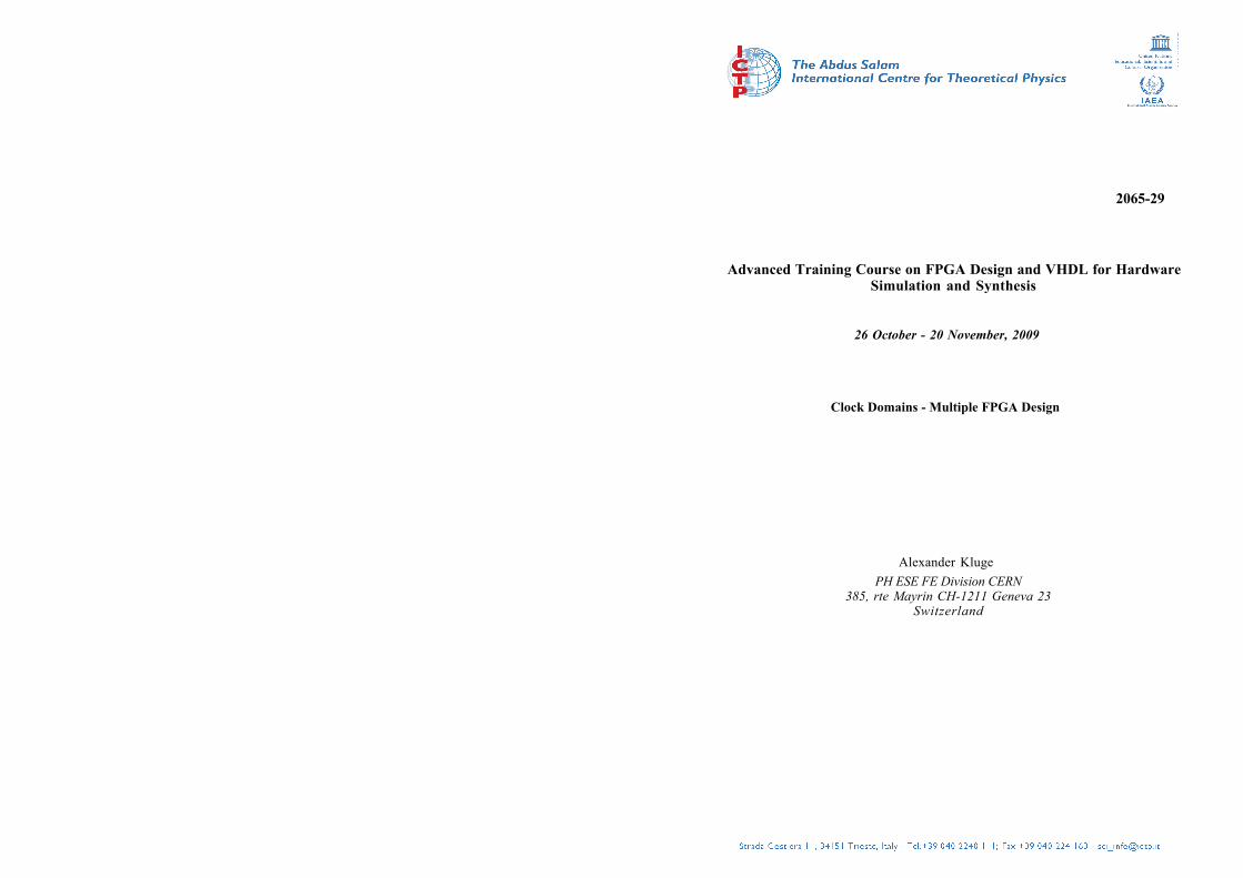
2065-29 Advanced Training Course on FPGA Design and VHDL for Hardware Simulation and Synthesis Alexander Kluge 26 October - 20 November, 2009 PH ESE FE Division CERN 385, rte Mayrin CH-1211 Geneva 23 Switzerland Clock Domains - Multiple FPGA Design
Transcript of 2065-29 Advanced Training Course on FPGA Design and VHDL...
2065-29
Advanced Training Course on FPGA Design and VHDL for HardwareSimulation and Synthesis
Alexander Kluge
26 October - 20 November, 2009
PH ESE FE Division CERN385, rte Mayrin CH-1211 Geneva 23
Switzerland
Clock Domains - Multiple FPGA Design

Clock domains –multiple FPGA design
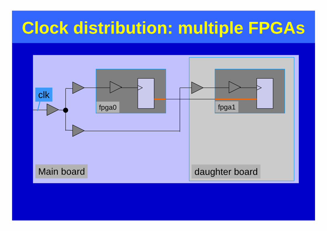
Clock distribution: multiple FPGAs
clk
Main board
fpga0 fpga1
daughter board
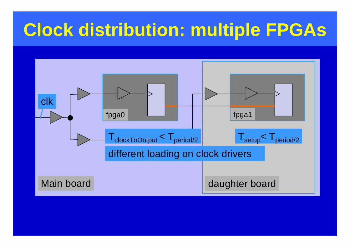
Clock distribution: multiple FPGAs
clk
Main board
fpga0 fpga1
daughter board
different loading on clock drivers
TclockToOutput < Tperiod/2 Tsetup< Tperiod/2
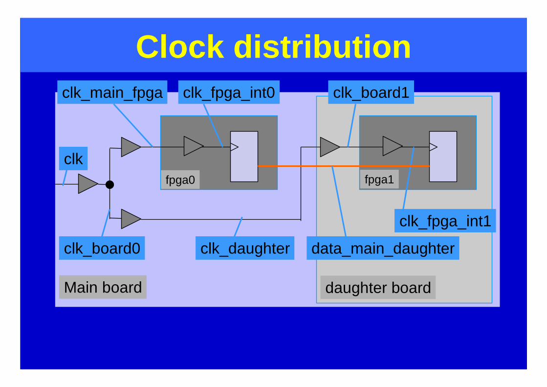
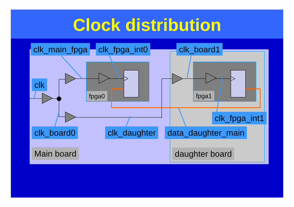
Clock distribution
clk
clk_board0 clk_daughter
clk_main_fpga clk_board1
clk_fpga_int1
clk_fpga_int0
data_main_daughter
Main board daughter board
fpga0 fpga1
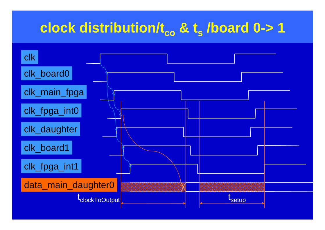
clock distribution/tco & ts /board 0-> 1
clk
clk_board0
clk_daughter
clk_main_fpga
clk_fpga_int0
clk_board1
clk_fpga_int1
data_main_daughter0tclockToOutput tsetup
Clock distribution
clk
clk_board0 clk_daughter
clk_main_fpga clk_board1
clk_fpga_int1
clk_fpga_int0
data_daughter_main
Main board daughter board
fpga0 fpga1

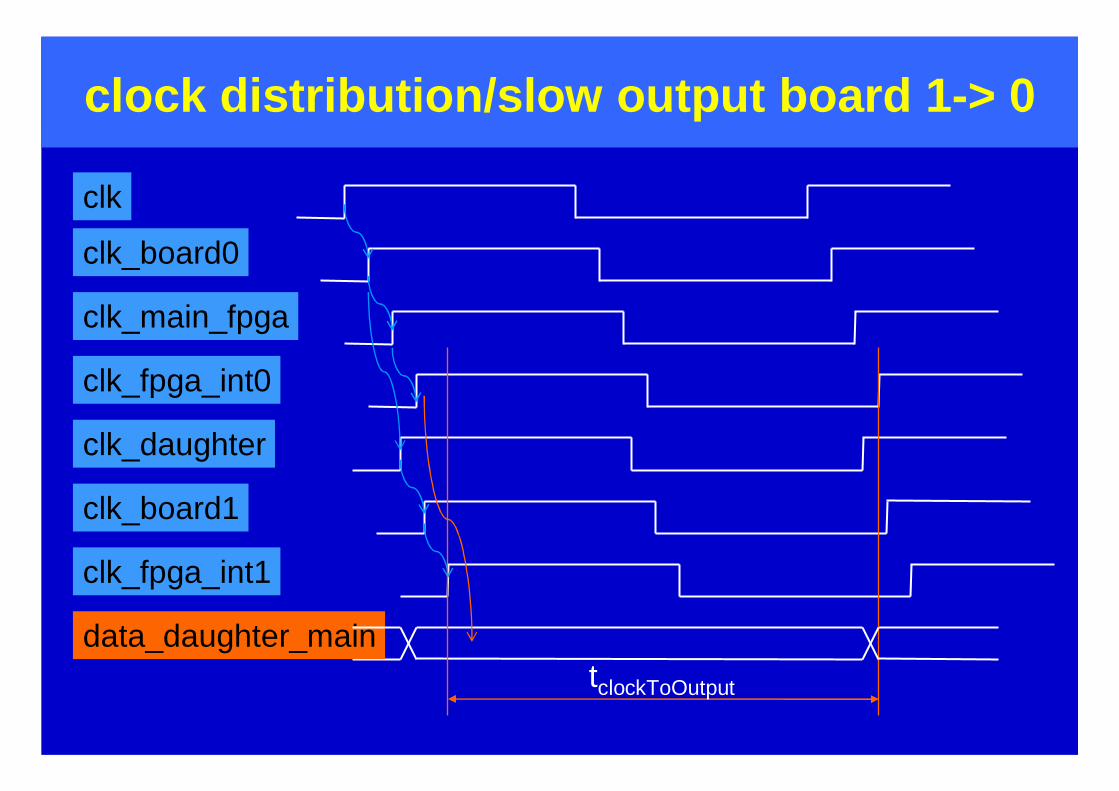
clock distribution/tco & ts /board 1-> 0
clk
clk_board0
clk_daughter
clk_main_fpga
clk_fpga_int0
clk_board1
clk_fpga_int1
data_main_daughter0tclockToOutput tsetup

Clock distribution
clk
clk_board0 clk_daughter
clk_main_fpga clk_board1
clk_fpga_int1
clk_fpga_int0
data_main_daughter
Main board daughter board
fpga0 fpga1

clock distribution/slow output board 0->1
clk
clk_board0
clk_daughter
clk_main_fpga
clk_fpga_int0
clk_board1
clk_fpga_int1
data_main_daughtertclockToOutput tsetup thold

clock distribution/fast output board 0->1
clk
clk_board0
clk_daughter
clk_main_fpga
clk_fpga_int0
clk_board1
clk_fpga_int1
data_main_daughtertclockToOutput

Clock distribution
clk
clk_board0 clk_daughter
clk_main_fpga clk_board1
clk_fpga_int1
clk_fpga_int0
data_daughter_main
Main board daughter board
fpga0 fpga1

clock distribution/fast output board 1-> 0
clk
clk_board0
clk_daughter
clk_main_fpga
clk_fpga_int0
clk_board1
clk_fpga_int1
data_daughter_maintclockToOutput tsetup thold
clock distribution/slow output board 1-> 0
clk
clk_board0
clk_daughter
clk_main_fpga
clk_fpga_int0
clk_board1
clk_fpga_int1
data_daughter_maintclockToOutput

Constraints• Fulfilling FPGA internal constraints is not
sufficient.• Perform system simulations• Logic can be too fast

Data selection & delay

collision
particle
detector electronics L0 Trigger
Event builder L2 Trigger
data storage
100 Tbyte/s
100 Gbyte/s
100 Mbyte/s
Data selection and delay
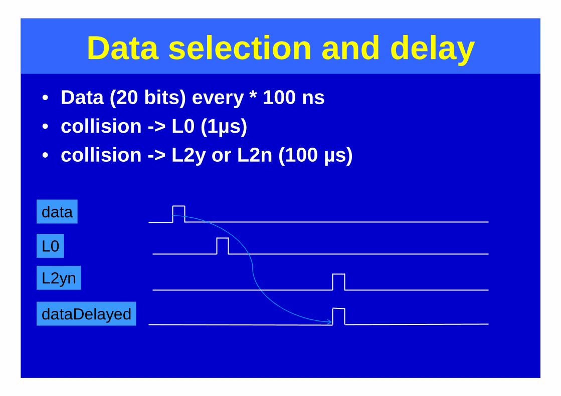
Data selection and delay• Data (20 bits) every * 100 ns• collision -> L0 (1µs)• collision -> L2y or L2n (100 µs)
data
L0
L2yn
dataDelayed

Data selection and delay• Data (20 bits) every * 100 ns• collision -> L0 (1µs)• collision -> L2y or L2n (100 µs)
• Options:– Data pipeline until L2 with FIFO based on shift
registers @ 10 MHz20 bits * 100 µs / 100 ns 20 bits * 1000 = 20 000 bits
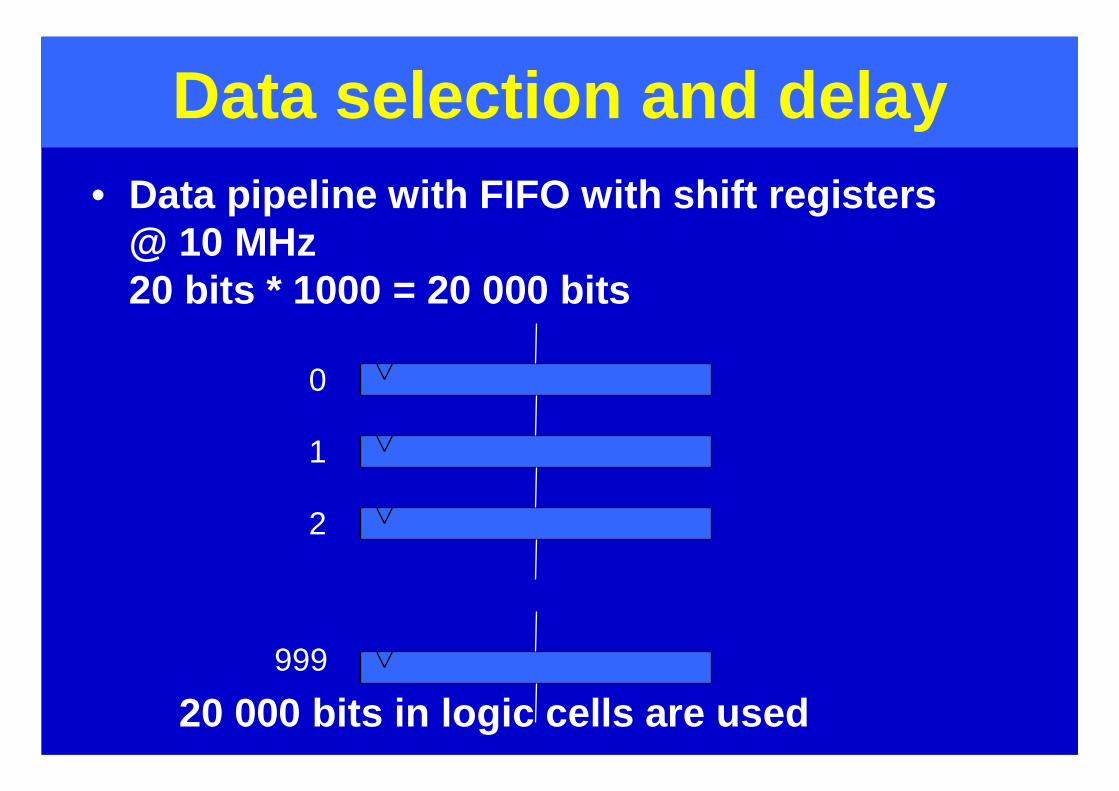
Data selection and delay• Data pipeline with FIFO with shift registers
@ 10 MHz20 bits * 1000 = 20 000 bits
0
1
2
999
20 000 bits in logic cells are used
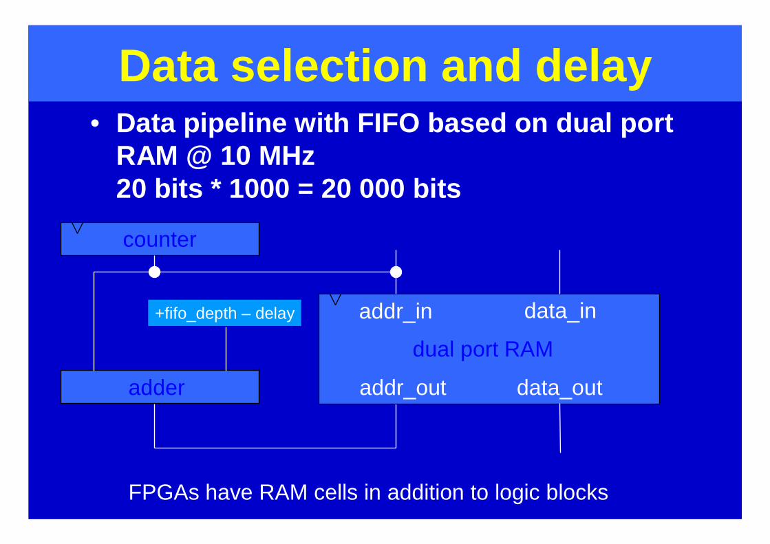
Data selection and delay• Data pipeline with FIFO based on dual port
RAM @ 10 MHz20 bits * 1000 = 20 000 bits
dual port RAM
data_in
data_out
addr_in
addr_out
counter
adder
+fifo_depth – delay
FPGAs have RAM cells in addition to logic blocks
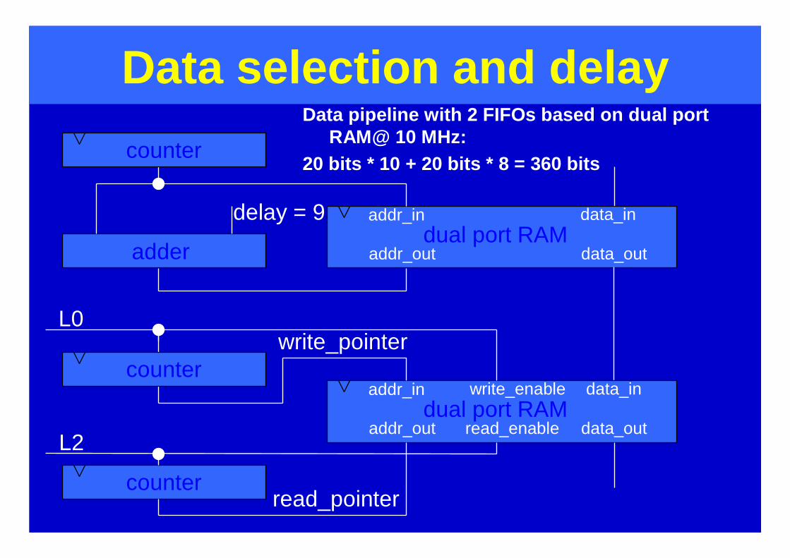
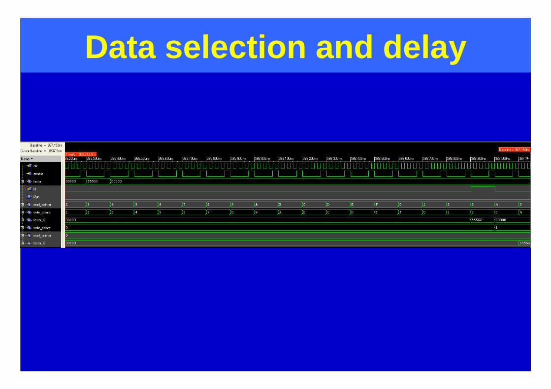
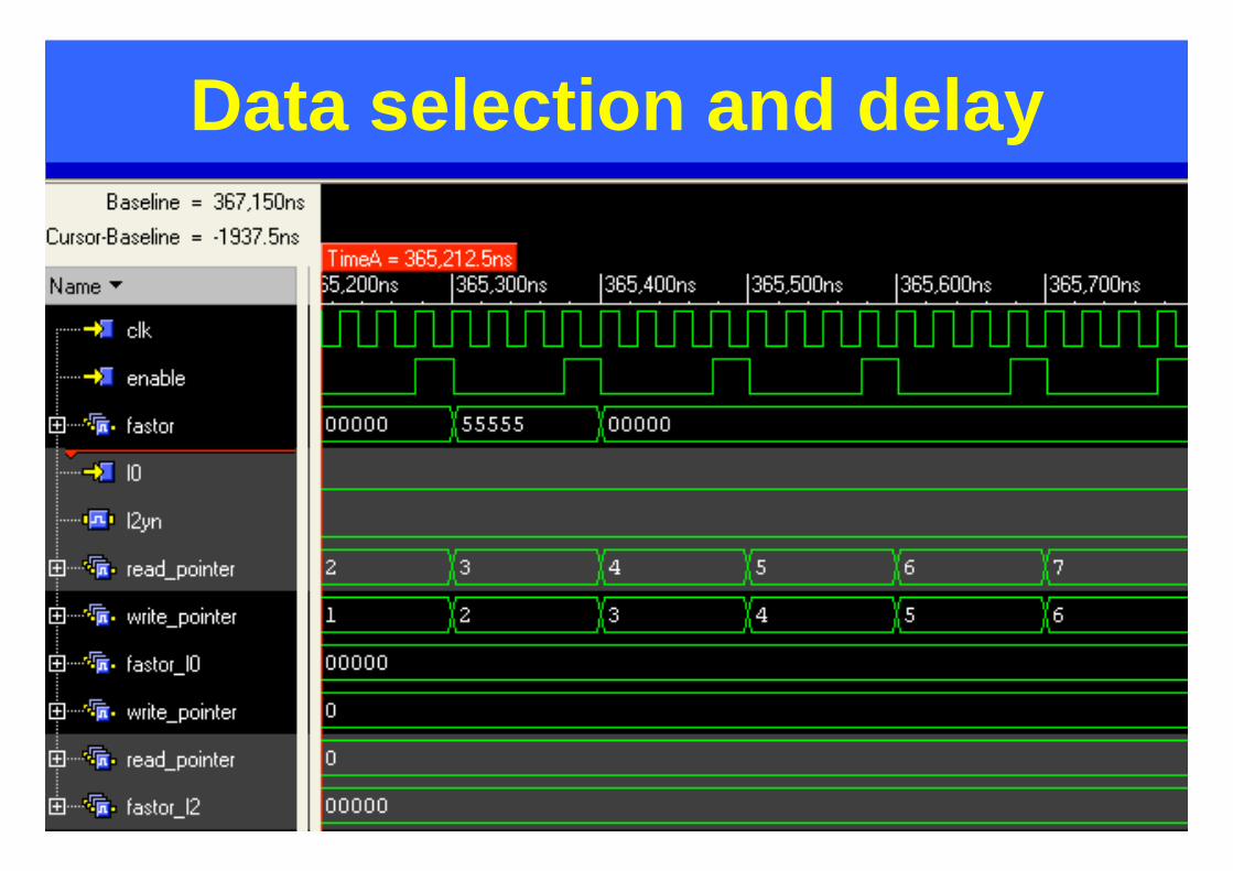
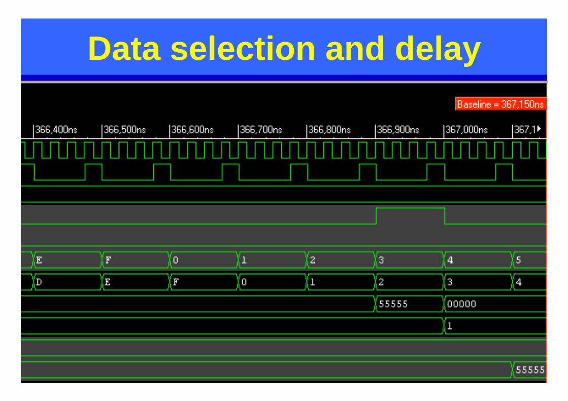
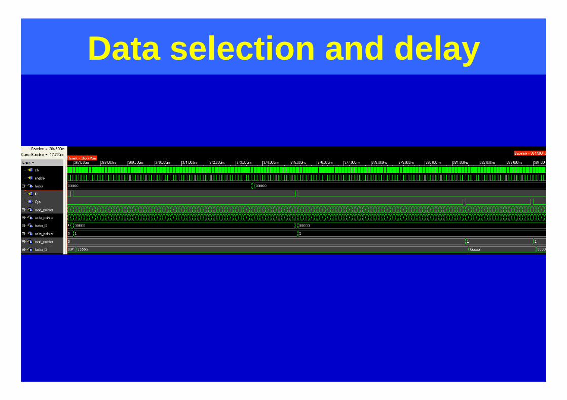
Data selection and delayData pipeline with 2 FIFOs based on dual port
RAM@ 10 MHz:20 bits * 10 + 20 bits * 8 = 360 bits
dual port RAMdata_in
data_out
addr_in
addr_out
counter
adder
delay = 9
dual port RAMdata_in
data_out
addr_in
addr_out
counter
counter
write_pointer
read_pointer
L0
L2
write_enable
read_enable

Data selection and delay
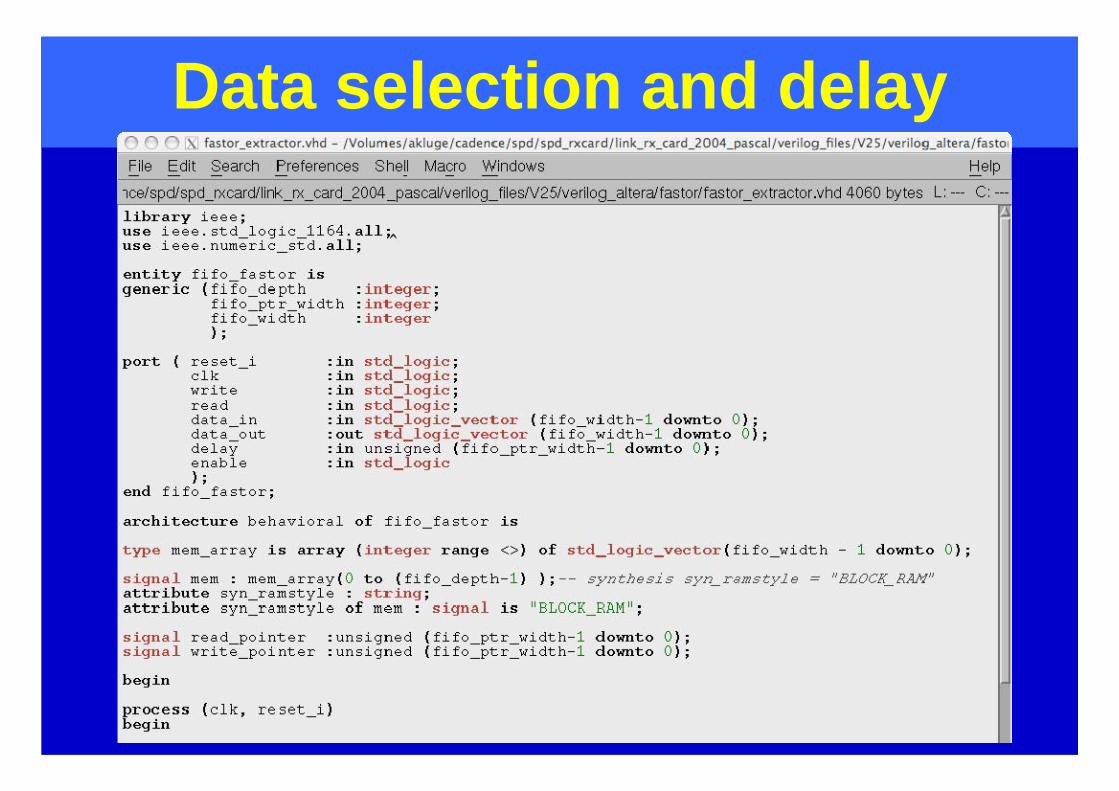
Data selection and delay
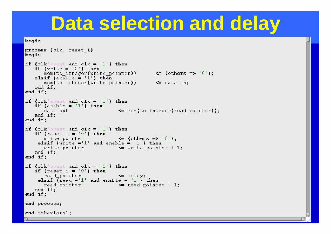
Data selection and delay

Data selection and delay

Data selection and delay

Data selection and delay

Data selection and delay
Data selection and delay
Data selection and delay
Data selection and delay
Data selection and delay

Data selection and delay
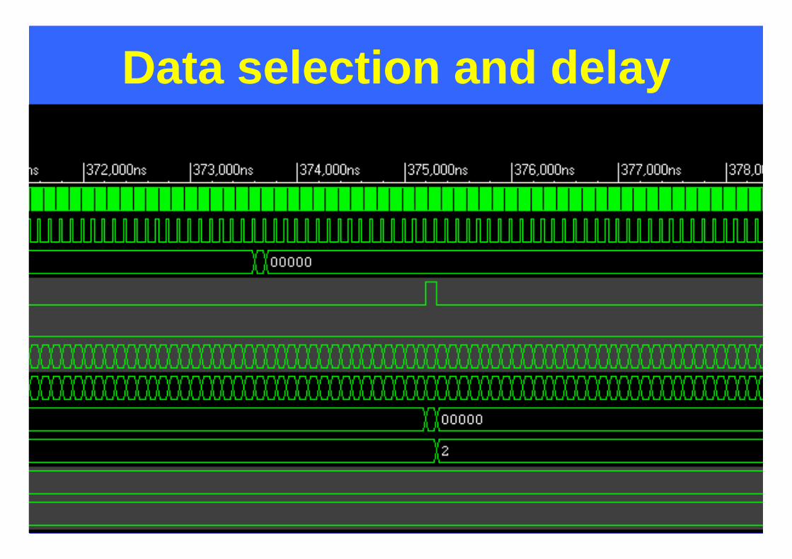
Data selection and delay

Data selection and delay
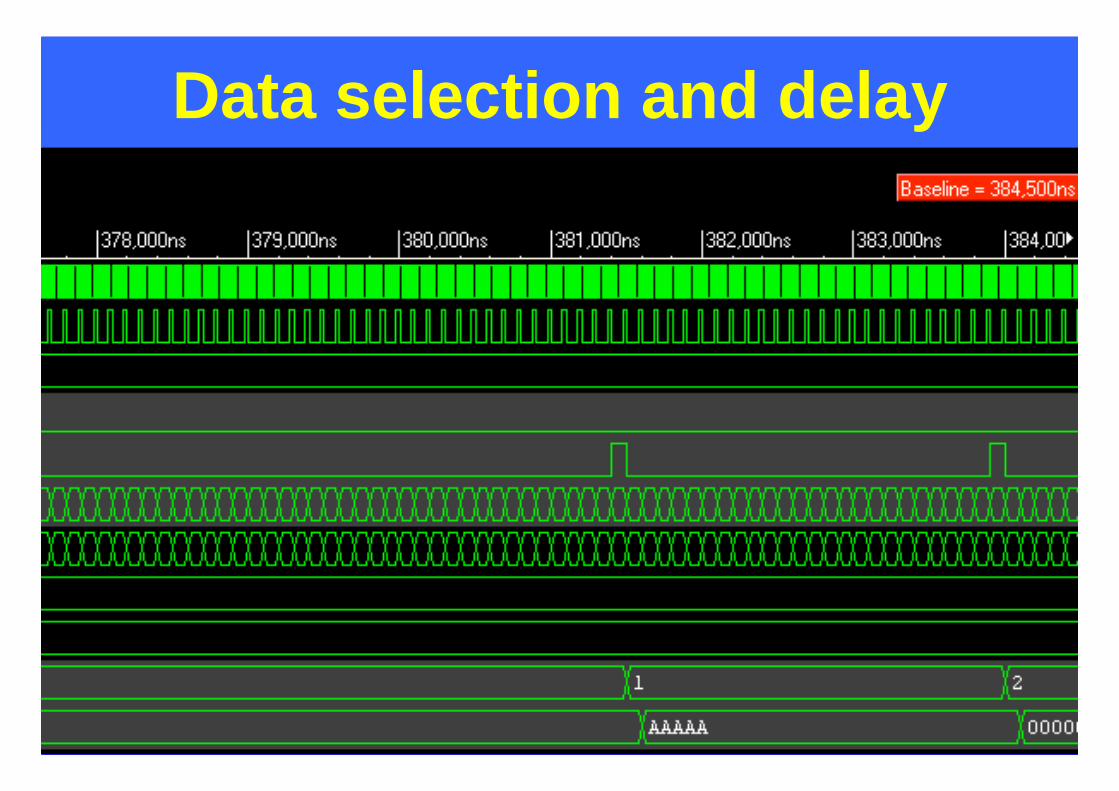
Data selection and delay
System level simulation

System level simulation
• 60 ASICs: simplified behavioral• 40 ASICs: full behavioral• 5 FPGA: full behavioral• 7 SRAMs: full behavioral• 4 PCBs
6 x 10
1 x
3 x
6 x

What happens if we have speed problems?
• Often because of inadequate logic architecture/coding style– evaluate logic architecture– rewrite HDL code to adapt structure to better
data throughput– insert pipeline structure - often one clock
cycle more latency does not matter– Understand the specifications– look for systematics which can help to
simplify logic– adapt architecture and schematics/code– only then optimize placing & routing

• Often because of components too small and routing congestion– timing constraints– Routing constraint - placement constraint– Use bigger/faster component
What happens if we have speed problems?
Conclusion• FPGA application at CERN
– data selection/trigger (muon track finder trigger)
– data processing (pixel detector)• Design cycle• Defining Specifications• Clock domains• Data delay