
©2015 Rut Rivera-Beltrán ALL RIGHTS RESERVED
193
©2015 Rut Rivera-Beltrán ALL RIGHTS RESERVED
Transcript of ©2015 Rut Rivera-Beltrán ALL RIGHTS RESERVED

©2015
Rut Rivera-Beltrán
ALL RIGHTS RESERVED

BISMUTH FERRITE BASED THIN FILMS, NANOFIBERS, AND FIELD
EFFECT TRANSISTOR DEVICES
by
RUT RIVERA – BELTRAN
A Dissertation submitted to the
Graduate School-New Brunswick
Rutgers, The State University of New Jersey
In partial fulfillment of the requirements
For the degree of
Doctor of Philosophy
Graduate Program in Materials Science and Engineering
Written under the direction of
Prof. Ahmad Safari
And approved by
__________________________
__________________________
__________________________
__________________________
New Brunswick, New Jersey
January, 2015

ii
ABSTRACT OF THE DISSERTATION
Bismuth Ferrite Based Thin Films, Nanofibers and Field Effect Transistor Devices
By RUT RIVERA – BELTRAN
Dissertation Director:
Prof. Ahmad Safari
In this research an attempt has been made to explore bismuth ferrite thin films with
low leakage current and nanofibers with high photoconductivity. Thin films were
deposited with pulsed laser deposition (PLD) method. An attempt has been made to
develop thin films under different deposition parameters with following target
compositions: i) 0.6BiFeO3-0.4(Bi0.5K0.5)TiO3 (BFO-BKT) and ii) bi-layered
0.88Bi0.5Na0.5TiO3–0.08Bi0.5K0.5TiO3–0.04BaTiO3/BiFeO3 (BNT-BKT-BT/BFO). BFO-
BKT thin film shows suppressed leakage current by about four orders of magnitude
which in turn improve the ferroelectric and dielectric properties of the films. The
optimum remnant polarization is 19 µC.cm-2
at the oxygen partial pressure of 300 mtorr.
The BNT-BKT-BT/BFO bi-layered thin films exhibited ferroelectric behavior as: Pr =
22.0 µC.cm-2
, Ec = 100 kV.cm-1
and r = 140. The leakage current of bi-layered thin films
have been reduced two orders of magnitude compare to un-doped bismuth ferrite.
Bismuth ferrite nanofibers were developed by electrospinning technique and its
electronic properties such as photoconductivity and field effect transistor performance

iii
were investigated extensively. Nanofibers were deposited by electrospinning of sol-gel
solution on SiO2/Si substrate at driving voltage of 10 kV followed by heat treatment at
550 ◦C for 2 hours. The composition analysis through energy dispersive detector and
electron energy loss spectroscopy revealed the heterogeneous nature of the composition
with Bi rich and Fe deficient regions. X-ray photoelectron spectroscopy results confirmed
the combination of Fe3+
and Fe2+
valence state in the fibers. The photoresponse result is
almost hundred times higher for a fiber of 40 nm diameter compared to a fiber with 100
nm diameter. This effect is described by a size dependent surface recombination
mechanism. A single and multiple BFO nanofibers field effect transistors devices were
fabricated and characterized. Bismuth ferrite FET behaves as p-type semiconductor. The
carrier mobility for a single nanofiber FET was found as 0.2 cm2/V.s at 100 V driving
voltage, while the carrier mobility of multiple nanofibers FET was maintained at 10 V
driving voltage.
The results of this study present the versatility of BFO in the form of thin films and
nanofibers for different electronic applications such as ferroelectric memories, transistor
and light sensor.

iv
Acknowledgments
First, I would like to thanks God for allowing me to reach this point in my career and
for giving me the strength to succeed. “God, thank you for always strength my inner man
to overcome the most challenge situations and obstacles ”. I would also like to thank my
advisor, Prof. Safari for not only being a great mentor but a father, mother, brother and
even more than a friend. Working in his group gave me the freedom and support to
follow my curiosity and develop new ideas in my project. I would also like to express my
gratitude to my thesis committee members: Prof. Chhowalla, Prof. Klein and Dr. Abazari.
Thanks to all of them for the guidance and invaluable comments to complete this task.
Many thanks to Dr. Wielunski and Dr. Yakshinskiy for helping with RBS measurements
and data analysis, to Dr. Tom Emge for XRD analysis in the Chemistry Department,
Mahsa Sina and Rajesh Kappera for TEM imaging and device characterization
respectively.
Once I moved to Rutgers, far from my family and love ones a new life began. Many
months of loneliness, tears and very tough times occurred. It was hard to stand, to go
further but God sent me very important people to take care of me during the valley.
Mercedes the MSE building janitor, being the only Spanish speaking person, close to my
culture, took care of all my needs in the building. Even in moments when my tears could
not be stopped, she was present to encourage and make me strong. Mehdi, Elaheh, Hulya,
Berra, Cecilia, Damien you are great friends, and classmates, I will appreciate the
memorable moments we shared. To all my friends from Puerto Rico here, at Rutgers,
especially to Mayda and Ernesto; thank you for your friendship. Yeslin, I appreciate your

v
friendship very much and will keep our relationship in my heart throughout the years.
Thank you for the phone calls, encouraging words, trust and confidence.
To my family-parents, brothers, grandparents, cousins and uncles… thanks to all of
you for the motivation and for believing in me. To my fiancé, friend and soul-mate in the
far distance for three years and now my husband, Heraldo, thank you for standing beside
me. It was tough to be far from each other but in the midst of the difficulties, in the good
and bad times, you always found the way to express your love and care. I love you,
because you love me! Thank you because you gave the best of yourself to make me feel
strong, happy and loved all the time. Now you are here to finish this race along with me
and appreciate all what you have done.
Finally, and most important, I would like to dedicate this thesis to my Parents, Iris
and José. Being the youngest of three siblings and the only girl put me in a position to
develop a closer relationship and bond with them. Thank you for respecting me, for being
my number one fan, for believing me. Even though it was hard for you when I decided to
move from home, you always supported and guided me to achieve the best in my career. I
still remember doing Skype with Mom, while I was studying, after leaving the lab at one
o’clock in the morning and you were there to walk me home through the phone. You
always have been there for me, never complaining about the late hours, the lack of sleep
or anything. I may felt Dad was not phone-calling so often, but he will be aware of what
was happening. At the right moment he called and says the right words to make me feel
better and encourage me to keep going forward. Dad always had the love and wisdom to
touch my heart and give me the peace I was looking for. Thank you for being present in
each step of my life and career. Love you Mom & Dad!

vi
Table of Contents
ABSTRACT …………………………………………………………………………….. ii
ACKNOWLEDGEMENTS …………………………………………………………….. iv
TABLE OF CONTENTS ………………………………………………………………. vi
LIST OF FIGURES ……………………………………………………………………... x
LIST OF TABLES …………………………………………………………………….. xix
1 Research Objectives and Scope of the Dissertation
1.1 Statement of the problem ……………………………………………………....... 1
1.2 Objectives ……………………………………………………………………….. 4
1.3 Thesis organization ……………………………………………………………… 5
1.4 References …………………………………………………….............................. 7
2 Introduction and Background
2.1 Introduction ……………………………………………………………………… 8
2.2 Dielectric materials ……………………………………………………………… 9
2.3 Piezoelectricity ……………………………………………………………......... 13
2.4 Ferroelectric materials ……………………………………………………......... 15
2.5 Ferromagnetism………………………………………………………………… 21
2.6 Multiferroic phenomenon and materials ……………………………………….. 24
2.7 Semiconductor materials ………………………………………………….......... 27
2.8 Summary …………………………………………………….............................. 35
2.9 References……………………………………………………............................. 36
vii
3 Literature Review
3.1 Introduction …………………………………………………………………….. 37
3.2 Bismuth ferrite ……………………………………………………………......... 38
3.3 Bismuth ferrite nanostructures ……………………………………………......... 44
3.3.1 Zero dimension (0D, Nanoparticles) …………………………………........ 46
3.3.2 One dimension (1D, Nanowires, Nanotubes) ……………………………... 49
3.3.3 Two dimension (2D, Thin films) ………………………………………….. 52
3.4 Summary ……………………………………………………………………….. 62
3.5 References ……………………………………………………………………… 63
4 Characterization and Equipment Tools
4.1 Introduction …………………………………………………………………….. 66
4.2 X-ray diffraction ………………………………………………………….......... 67
4.3 Rutherford backscattering spectrometry ………………………………….......... 70
4.4 Raman spectroscopy ………………………………………………………….... 72
4.5 Electron microscope: transmission electron microscope and scanning electron
microscope …………………………………………………………………………. 76
4.6 Electron energy loss spectroscopy ……………………………………………... 79
4.7 Electrical Characterization ……………………………………………………... 81
4.7.1 Current vs voltage & current vs time ........................................................... 82
4.7.2 Ferroelectric and dielectric measurements ………………………………... 83
4.8 Summary…………………………………………………………....................... 83
4.9 References ………………………………………………………….................... 84
viii
5 Bismuth Ferrite Thin Films by Sol-Gel
5.1 Introduction …………………………………………………………………….. 94
5.2 Experimental procedure ………………………………………………………... 95
5.3 Results and discussion ……………………………………………………….. .. 97
5.4 Summary ……………………………………………………………………… 105
5.5 References …………………………………………………………………….. 106
6 Bismuth Ferrite Thin Films by Pulsed Laser Deposition
6.1 Introduction …………………………………………………………………….. 99
6.2 Experimental procedure ………………………………………………………. 100
6.2.1 Powder and target preparation …………………………………………... 100
6.2.2 Laser deposition system …………………………………………………. 103
6.2.3 Pulsed laser deposition standard procedure ……………………................ 104
6.2.4 Deposition of bottom electrode ………………………………………….. 107
6.2.5 Deposition of top electrode ………………………………………............ 107
6.3 Bismuth ferrite based thin films ………………………………………………. 108
6.3.1 Bismuth ferrite …………………………………………………………… 108
6.3.2 Effect of oxygen pressure on 0.6BiFeO3-0.4(Bi0.5K0.5)TiO3 ……………. 111
6.3.3 BiFeO3/ (Bi0.5Na0.5)TiO3-(Bi0.5K0.5)TiO3-BaTiO3 bi-layered .................... 122
6.3.4 Summary …………………………………………………………............ 127
6.3.5 References ……………………………………………………………….. 128

ix
7 Bismuth Ferrite Nanofibers by Electrospinning
7.1 Introduction ……………………………………………………………….. 130
7.2 Experimental procedure …………………………………………………... 131
7.2.1 Electrospinning setup …………………………………………. 131
7.2.2 Standard operation procedure ……………………………….... 133
7.2.3 Sol gel solution preparation …………………………………... 135
7.3 Fabrication and characterization of bismuth ferrite nanofibers …………... 136
7.3.1 Optimization of solution and processing conditions ………….. 137
7.3.2 Characterization of bismuth ferrite nanofibers ……………….. 140
7.3.3 Nanofibers with different diameters ………………………….. 144
7.3.3.1 Grain size ……………………………………………... 147
7.3.3.2 Valence state ………………………………………….. 148
7.3.3.3 Chemical composition ………………………………... 149
7.4 Electrical properties of BFO nanofibers ………………………………….. 152
7.4.1 Single nanofibers ……………………………………………... 152
7.4.2 Size dependent on the photoconductivity of multiple-nanofibers
…………………………………………………………………. 154
7.5 Bismuth ferrite field effect transistor devices with single and multiple
nanofibers devices ………………………………………………………… 159
7.6 Summary …………………...…………………...…………………...……. 163
7.7 References …………………...…………………...…………………...…... 164
8 Conclusions …………………...…………………...…………………...………… 166
9 Suggestion for future work …………………...…………………...……………. 171

x
List of Figures
Figure 2.1 A parallel plate capacitor (a) when a vacuum is present and (b) when a
dielectric material is inserted…………………………………………………………… 10
Figure 2.2 Polarization mechanisms leading to dielectric polarization/displacement…. 11
Figure 2.3 Variation of dielectric constant with frequency of alternating electric field.
Electronic, ionic, orientation and space charge contributions to the dielectric constant are
indicated ………………………………………………………………………………... 12
Figure 2.4 The crystal structure of barium titanate (perovskite structure). (a) Above Curie
temperature the cell is cubic and (b) below the Curie temperature is tetragonal with Ba2+
and Ti4+
ions shifted relative to the O2-
ions …………………………………………… 16
Figure 2.5 Temperature dependence of the dielectric constant in barium titanate…….. 17
Figure 2.6 Barium titanate phase transition below TC ………………………………… 17
Figure 2.7 Typical hysteresis loop …………………………………………………….. 19
Figure 2.8 (a) ionic displacement in two 180◦ ferroelectric domains, (b) domain structure
is showing several 180◦ domains of different sizes and (c) 180
◦ domain wall with a width
of ~ 0.2 -0.3 nm ……………………………………………………………………….... 20
Figure 2.9 Order arrangements of electron spins ……………………………………… 21
Figure 2.10 A magnetization hysteresis loop for a ferromagnetic material. Insets: domain
structures at various magnetic fields …………………………………………………… 22
xi
Figure 2.11 The origin of ferromagnetic domains. (a) single domain as a consequence of
the magnetic “poles” formed on the surfaces, (b) the magnetic is energy is reduced
approximately one half by dividing the crystal into two domains magnetized in opposite
directions, (c) with N domains the magnetic energy is reduced to approximately 1/N of
the magnetic energy of a single domain, (d) and (e) in such domain arrangement the
magnetic energy is zero ………………………………………………………………... 23
Figure 2.12 Multiferroic combined the properties of ferroelectrics and magnets …….. 24
Figure 2.13 The energy band structure for (a) metal, (b) insulator and (c) semiconductor
…………………………………………………………………………………………... 28
Figure 2.14 Extrinsic semiconductor (a) n-type: an impurity atom such as phosphorus
with five valence electrons may substitute for a silicon atom resulting in an extra bonding
electron, (b) p-type: an impurity atom such as boron with three valence electrons may
substitute for silicon atom resulting in a deficiency of a one valence electron ………... 30
Figure 2.15 For a p-n rectifying junction representation of electron and hole distributions
for (a) non electrical potential, (b) forward bias and (c) reverse bias ………………….. 32
Figure 2.16 Photoexcitation in semiconductors ……………………………………….. 35
Figure 3.1 (a) Hysteresis loop measured at 15 kHz showing high remnant polarization
~55 C/cm2, and (b) magnetic hysteresis loop for 70 nm BFO film with an appreciable
saturation magnetization of 150 emu/cm3, and a coercive field of 200 Oe. NOTE: The in-
plane loop is shown in blue, and the out-of-plane loop is in red ………………………. 38
Figure 3.2 Perovskite crystal structure of bulk BiFeO3 ……………………………….. 39
xii
Figure 3.3 Schematic representation of bismuth ferrite spin cycloid. The canted
antiferromagnetic spins (blue and green) give rise to a net magnetic moment (purple
arrows) that is spatially averaged out to zero due to the cycloidal rotation ……………. 41
Figure 3.4 (a) 71◦ domain boundary with continuous oxygen octahedral rotations,
(b) 109◦ domain boundary with continuous oxygen octahedral rotation centered on the
FeO2 plane, and (c) 180◦ domain boundary with continuous oxygen octahedral
rotations ………………………………………………………………………………… 43
Figure 3.5 (a) Topography of BFO thin films with roughness (rms) of 0.5 nm, (b) In-
plane PFM image of a written domain pattern in a mono-domain BFO (110) film showing
all three types of domain wall, that is, 71◦
(blue), 109◦
(red) and 180◦ (green), and (c)
corresponding c-AFM image showing conduction at both 109◦ and 180
◦ domain walls;
note the absence of conduction at the 71◦ domain walls ……………………………….. 43
Figure 3.6 (a) Hysteresis loop at 300 K for bismuth ferrite nanoparticles, and (b) Size, d
represents the diameter of the as-prepared nanoparticles. Ms is the magnetization
observed at H = 50 kOe. Hc and Hx represent derived coercivities and exchange bias
parameters, respectively ………………………………………………………………... 47
Figure 3.7 Raman Spectra of bismuth ferrite nanoparticles with size of: (a) 14 nm, (b) 41
nm, (c) 51nm, (d) 75 nm, (e) 95 nm, (f) 245 nm, and (g) 342 nm, respectively as well as
of the bulk (h). The Si peaks are identified with an asterisk. The arrow is referring to the
A1 mode at 136 cm-1
…………………………………………………………………… 47
Figure 3.8 (a) Absorption coefficient at 300 K for bulk and 16 nm bismuth ferrite, and
(b) close up view of A1(TO1) phonon mode at 300 K …………………………………. 48

xiii
Figure 3.9 Absorption coefficient of 16 nm bismuth ferrite nanoparticle as compared
with epitaxially grown rhomobohedral thin film. Inset: Direct band gap analysis of the
thin film and nanoparticles ……………………………………………………………... 49
Figure 3.10 (a) Scanning electron microscope image of crystallize bismuth ferrite
nanofibers, and (b) magnetic hysteresis loop …………………………………………... 50
Figure 3.11 (a) Diameter dependence of the room temperature raman spectra of the co-
doped bismuth ferrite nanowires, and (b) diameter dependent variation of the magnetic
hysteresis loops of the co-doped nanowires measured at 300K ……………………….. 51
Figure 3.12 Polarization hysteresis loops compositions of x = 0.1, 0.14 and 0.16
(a) 5 kHz, and (b) 25 kHz ……………………………………………………………… 53
Figure 3.13 (a) Dielectric constant 33 and tan measured at 1 MHz (zero bias), and (b)
High field d33 determined from piezoelectric hysteresis loop measured as a function of
composition (not shown here) ………………………………………………………….. 54
Figure 3.14 (a) Hysteresis loop of BLFO-PZT thin films measured at 5 kHz, and (b)
Dielectric properties measured at 1 kHz ……………………………………………….. 55
Figure 3.15 (a) Hysteresis loops for (a) single layer BNT thin film, (b) single layer BFO
thin film, and (c) bi-layered BFO/BNT thin film ……………………………………… 57
Figure 3.16 (a) Frequency dependent of dielectric behavior, and (b) dc conductivity vs
1/T at different frequencies for the bi-layered BFO/BNTBT thin film ………………... 58
Figure 3.17 (a) [003] peaks from x-ray scans showing the effect of film thickness on
epitaxial strain. As the film thickness increased, the peak position progressively increases
(black line, 70 nm; red line, 100 nm; blue line, 200 nm; and green line, 400 nm), and (b)
small signal d33 for a 50 m capacitor …………………………………………………. 59
xiv
Figure 3.18 Pressure-temperature phase diagram for BFO thin films with a thickness of
70 nm …………………………………………………………………………………... 60
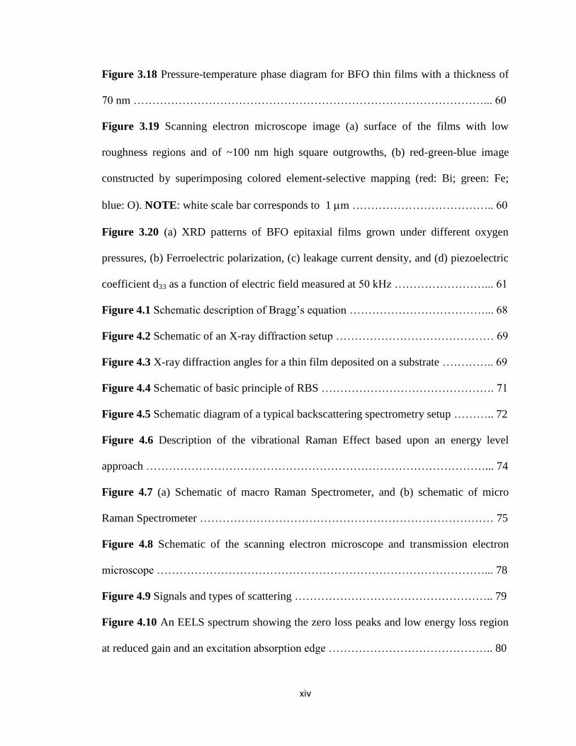
Figure 3.19 Scanning electron microscope image (a) surface of the films with low
roughness regions and of ~100 nm high square outgrowths, (b) red-green-blue image
constructed by superimposing colored element-selective mapping (red: Bi; green: Fe;
blue: O). NOTE: white scale bar corresponds to 1 m ……………………………….. 60
Figure 3.20 (a) XRD patterns of BFO epitaxial films grown under different oxygen
pressures, (b) Ferroelectric polarization, (c) leakage current density, and (d) piezoelectric
coefficient d33 as a function of electric field measured at 50 kHz ……………………... 61
Figure 4.1 Schematic description of Bragg’s equation ………………………………... 68
Figure 4.2 Schematic of an X-ray diffraction setup …………………………………… 69
Figure 4.3 X-ray diffraction angles for a thin film deposited on a substrate ………….. 69
Figure 4.4 Schematic of basic principle of RBS ………………………………………. 71
Figure 4.5 Schematic diagram of a typical backscattering spectrometry setup ……….. 72
Figure 4.6 Description of the vibrational Raman Effect based upon an energy level
approach ………………………………………………………………………………... 74
Figure 4.7 (a) Schematic of macro Raman Spectrometer, and (b) schematic of micro
Raman Spectrometer …………………………………………………………………… 75
Figure 4.8 Schematic of the scanning electron microscope and transmission electron
microscope ……………………………………………………………………………... 78
Figure 4.9 Signals and types of scattering …………………………………………….. 79
Figure 4.10 An EELS spectrum showing the zero loss peaks and low energy loss region
at reduced gain and an excitation absorption edge …………………………………….. 80

xv
Figure 4.11 The sample is placed under the light source. (a) Light On, (b) Light Off, and
(c) Current vs Time plot upon sample illumination ……………………………………. 82
Figure 5.1 Flowchart of sol-gel deposition procedure ………………………………… 87
Figure 5.2 X-ray diffraction patterns for BFO-Mn doped thin films ………………….. 89
Figure 5.3 Raman Spectroscopy for BiFe1-xMnxO3 thin films as function of Mn content
…………………………………………………………………………………………... 90
Figure 5.4 FESEM micrographs of BiFe1-xMnxO3 thin film surface (left side) and cross
section (right side). (a-b) x = 0.00, (c-d) x = 0.05, (e-f) x = 0.10, and (g-h) x = 0.15
………………………………………………………………………………................... 92
Figure 5.5 (a) Polarization hysteresis loop for BFO thin film, (b) Polarization hysteresis
loop for BiFe0.95Mn0.05O3 thin film, and (c) leakage current as a function of electric field
for BFO and BFMO thin film Note: 20 layers is equivalent to an overall thickness of
200 nm …………………………………………………………………………………. 95
Figure 6.1 Schematic of three different thin film design deposited by PLD ………….. 99
Figure 6.2 Flowchart for the preparation of bismuth ferrite ceramic target by solid oxide
method ………………………………………………………………………………… 101
Figure 6.3 Schematic diagram of the deposition system used for laser ablation ……...103
Figure 6.4 FESEM surface image of (a) BFO (inset: BFO cross section), and (b) BFO-La
doped thin film ………………………………………………………………………... 109
Figure 6.5 X-ray diffraction pattern for pure BFO thin film ………………………… 109
Figure 6.6 Polarization-Electric Field (P-E) hysteresis loop for single layer bismuth
ferrite thin film measured at 1 kHz and room temperature …………………………… 110
xvi
Figure 6.7 X-ray diffraction pattern for BFOBKT thin films deposited at (a-b) 300
mTorr, (b-c) 400 mTorr, and (c-d) 500 mtorr. The left side images (a, c, d) are for 200,
and right side images (b, d, e) are for 400 integration ………………………………... 112
Figure 6.8 Field emission SEM micrographs of surface and cross section for BFO-BKT
thin films deposited under different oxygen pressure. (a-b) 300 mtorr, (c-d) 400 mtorr,
and (e-f) 500 mTorr …………………………………………………………………... 115
Figure 6.9 RBS spectrum for BFO-BKT thin film deposited at different oxygen pressure
…………………………………………………………………………………………. 116
Figure 6.10 (a) Polarization-Electric field (P-E) loops and (b) leakage current
characteristics for BFOBKT thin films deposited in a range of oxygen partial pressure of
300 – 500 mTorr ……………………………………………………………………… 120
Figure 6.11 Dielectric properties of BFO-BKT thin films deposited in a range of oxygen
partial pressure of 300 – 500 mTorr (a) relative dielectric constant, and (b) dielectric loss
…………………………………………………………………………………………. 121
Figure 6.12 X-ray diffraction pattern for BFO/BNT-BKT-BT bi-layered thin film near
the (a) 002 integration, and (b) 400 integration ………………………………………. 122
Figure 6.13 FESEM surface image of BFO/BNT-BKT-BT bi-layered. NOTE: Top layer
is BFO ………………………………………………………………………………… 123
Figure 6.14 (a) P-E loop for BFO/BNT-BKT-BT bi-layered thin film, and (b) leakage
current characteristics for BFO, BNT-BKT-BT, and BFO/BNT-BKT-BT thin films
…………………………………………………………………………………………. 125
Figure 6.15 Dielectric properties of BFO/BNT-BKT-BT bi-layered thin film (a) relative
dielectric constant, and (b) dielectric loss …………………………………………….. 126
xvii
Figure 7.1 Schematic for electrospinning setup ……………………………………… 131
Figure 7.2 Nanofibers deposited at separated distance between the needle and collector
of (a) 15, (b) 20, (c) 25, and (d) 30 cm ……………………………………………….. 139
Figure 7.3 X-ray diffraction pattern for a BFO thin film of the same precursor solution as
the nanofibers …………………………………………………………………………. 140
Figure 7.4 Raman Spectroscopy for 0.6M BFO nanofibers mat …………………….. 141
Figure 7.5 Transmission electron microscope (TEM) image for a 100 nm nanofibers.
(a) surface image, and (b) diffraction pattern ………………………………………… 142
Figure 7.6 SEM surface micrographs for electrospun nanofibers of different precursor
solution concentrations. (a) 0.4M, (b) 0.6M, (c) 0.8M, (d) 1.0M, (e) 1.2M, and (f) 1.4M
…………………………………………………………………………………………. 145
Figure 7.7 Nanofibers diameter as a function of precursor solution concentration ….. 146
Figure 7.8 High resolution transmission electron microscope (HRTEM) image of a joint
BFO nanofibers ……………………………………………………………………….. 146
Figure 7.9 Average grain size as a function of fiber diameter obtained from TEM …. 147
Figure 7.10 Fe valence state as a function of fiber diameter obtained from EELS analysis
………………………………………………………………………………………… 149
Figure 7.11 Rutherford backscattering spectrometry results for 1.0 M (80 to100 nm in
diameter) BFO multiple-nanofibers …………………………………………………... 150
Figure 7.12 Rutherford backscattering spectrometry results for 0.8 M (50 to 70 nm in
diameter) BFO multiple-nanofibers …………………………………………………... 150
Figure 7.13 Rutherford backscattering spectrometry results for 0.6 M (30 to 50 nm in
diameter) BFO multiple-nanofibers …………………………………………………... 151
xviii
Figure 7.14 SEM surface images for BFO single nanofiber (a) top view of metal
electrode, (b-d) zoom in image of the nanofiber between each metal electrode ……... 152
Figure 7.15 Current vs Voltage for single nanofibers of different diameters at RT …. 153
Figure 7.16 Current vs time at constant voltage (10V) upon illumination …………... 154
Figure 7.17 On/Off ratio for a multiple-nanofibers mat as a function of average diameter
…………………………………………………………………………………………. 155
Figure 7.18 Plot of the On/Off ratio in comparison with BFO grain size and Fe state for
single nanofibers ……………………………………………………………………… 156
Figure 7.19 Band diagram for different nanofibers diameter. (a-b) completely depleted,
and (c) thin channel exits ……………………………………………………………... 158
Figure 7.20 (a) Schematic of device fabrication for BFO nanofiber field effect transistor.
In the case of a single nanofiber device there is only one fiber between drain and source
contacts. For a multiple-nanofibers device there are about ten nanofibers between drain
and source contacts …………………………………………………………………… 159
Figure 7.21 Field effect transistor device transfer characteristic for (a) single-nanofiber
device, and (b) multiple-nanofiber device ……………………………………………. 161
Figure 7.22 Field effect transistor device output characteristic for (a) single-nanofiber
device, and (b) multiple-nanofiber device ……………………………………………. 162

xix
List of Tables
Table 1.1 Piezoelectric properties of hard and soft PZT ………………………………... 2
Table 2.1 Thirty-two point groups in crystallography ………………………………… 14
Table 2.2 Mechanisms for Multiferroic ……………………………………………….. 26
Table 2.3 Summary of different field effect transistors types and operation requirements
…………………………………………………………………………………………... 34
Table 4.1 Comparison between TEM and SEM ………………………………………. 78
Table 5.1 Comparison of the Raman mode peak positions from the present study and the
literature ………………………………………………………………………………... 91
Table 6.1 Weight of raw materials for a 100 g batch of BiFeO3 ……………………... 102
Table 6.2 Weight of raw materials for a 100 g batch of 0.6BiFeO3-0.4(Bi0.5K0.5)TiO3
......................................................................................................................................... 102
Table 6.3 Weight of raw materials for a 100 g batch of 0.88(Bi0.5Na0.5)TiO3
0.08(Bi0.5K0.5)TiO3-0.04BaTiO3 ……………………………………………………… 102
Table 6.4 Peak integration parameters for (200) peak profiles ………………………. 113
Table 6.5 Bi/Fe ratio according to RBS simulation ………………………………….. 114
Table 6.6 Ferroelectric values for BFO based thin film solid solution ………………. 118
Table 7.1 Electrospinning processing optimization: Flow rate ……………………… 137
Table 7.2 Electrospinning processing optimization: Voltage ………………………... 137
Table 7.3 Electrospinning processing optimization: Spinning distance (between the
needle and the collector) .............................................................................................. 138
Table 7.4 d-spacing for single BFO nanofibers from TEM ………………………...... 143

xx
Table 7.5 Chemical composition for BFO multiple-nanofibers (mat) ……………….. 151

1
1 Research Objectives and Scope of the Dissertation
1.1 Statement of the problem
Lead-based Pb(Zr1-xTix)O3 (PZT) compositions near the morphotropic phase
boundary (x ~ 48%) have been the leading material for transducers applications because
of its high electromechanical properties described in Table 1.1. In a basic sense when a
piezoelectric material is subjected to a stress it generates an electric charge. The opposite
of this phenomenon holds true when an electric field is applied to a piezoelectric material
its shape deforms in proportion to the applied field. In comparison with early discovered
piezoelectric material such as barium titanate (BaTiO3), PZT exhibits stronger
electromechanical properties and higher operating temperature. Regardless of its
outstanding properties summarized in Table 1.1, PZT and related composition contains a
high content of lead. The lead content raises environmental concerns because of its
toxicity levels. The lower vapor pressure of lead oxide (PbO) and the required high
temperature during the processing results in lead evaporation. The lead is release to the
environment causing harmful effects to the ecosystem. The disposal and recycling
processes of lead based materials is another concern for those used in consumer products.
Therefore imperative measures have been taken to restrict the usage of lead based
composition for commercial applications. Many government regulations have been
enacted in respond to this inquiry such as the Restriction of Hazardous Substances
(RoHS) directives in Europe and China, the European RoHS directive restrict hazardous
substances (lead) used in electronic equipment 1. Thus, there is a great interest in the

2
development of environmental friendly, biocompatible, and lead free piezoelectric
materials.
Table 1.1 Piezoelectric properties of hard and soft PZT ceramics 2–4
Parameter Hard PZT4 * Soft PZT5H **
d33 (pC/N) 289 593
g33 (10-3
Vm/N) 26.1 19.7
kt 0.51 0.50
kp 0.58 0.65
Qm 500 65
EC (kV/cm) 18 15
TC(◦C) 328 193
r @ 1 kHz 1300 3400
tan @ 1kHz 0.004 0.02
*doped with acceptor ions such as K+ or Na
+ at the A site or Fe
3+, Al
3+ or
Mn3+
at the B site 2
** doped with donor ions such as La3+
at the A site or Nb5+
or Sb5+
at the
B site 2
In the past fifteen years there has been a significant increase in investigations and
development of lead free materials. Currently the lead free perovskite can be grouped in
two main families: (K0.5Na0.5)NbO3 (KNN) and (Bi0.5Na0.5)TiO3 (BNT). Despite the
effort to obtain similar piezoelectric properties to PZT, none of these compositions are
still ready to replace lead base compositions.
3
In recent years, bismuth ferrite (BiFeO3-BFO) has been considered a potential
candidate for the development of lead free ferroelectrics due to its high Curie
temperature, 1100 K and high Néel temperature, 650 K of antiferromagnetism 5,6
.
Theoretically, spontaneous polarization (PS) corresponds to [111] direction of
rhombohedral structure and is expected to display value of ≈ 100 C.cm-2
. Practical
applications of BFO are hindered because of the high leakage current at room
temperature.
Bismuth ferrite is also a unique material showing multiferroic (ferroelectric and
antiferromagnetism simultaneously) behavior at room temperature. Recently, BFO turn
out to be a potential candidate for optical applications 7,8
because of the favorable low
bandgap of 2.7 eV 9,10
that unlike other ferroelectric materials is in the visible range.
Anomalous in photoexcited voltage which exceeds the several times the band gap
limitations have been reported 11
. These effects make BFO attractive for photovoltaic
applications. However, a major limitation in practical applications is the low power
conversion efficiency 12
.
Even though the investigation on bulk bismuth ferrite exhibited poor ferroelectric
properties researchers continue to study this system. Report on the development of
bismuth ferrite epitaxial thin film (200 nm) by pulsed laser deposition with very high
spontaneous polarization further sparked the materials science community 13
. When the
particle size is reduced lower than antiferromagnetic periodicity (64 nm) the spiral
cycloid is suppressed and the magnetic properties become sizeable 14
. Since then (2003
to 2007), the research has evolved into a new scale searching for novel BFO based
compositions for future electronic applications.
4
1.2 Objectives
The purpose of this research was to develop BFO nanostructures (thin film and
nanofibers) and study the ferroelectric, optical, and semiconductor properties as potential
candidate for multifunctional applications. Along with the processing of bismuth ferrite
nanofibers, field effect transistors devices of such nanofibers were fabricated and their
electrical performance was evaluated.
On the thin film fabrication, the study was focused in the combination of bismuth
ferrite with other lead free compounds in the form of binary system and bi-layered
structure to couple, enhance the ferroelectric performance, and minimize the leakage
current. Accordingly the microstructure, phase, orientation, ferroelectric properties, and
leakage current were characterized.
1- Study the effect of controlled atmosphere on the ferroelectric properties of BFO-
BKT thin films.
2- Study the ferroelectric properties of BFO/BNT-BKT-BT bi-layered thin film
architecture.
3- Minimize the leakage current on Mn doped bismuth ferrite thin films.
5
Another objective of this research was on the development of BFO nanofibers as
outlined below:
1- Optimization of electrospinning sol-gel solution to fabricate nanofibers.
2- Investigate the microstructure, chemical composition, and crystalline phase of
deposited nanofibers.
4- Study the optical properties for opto-electronic applications.
5- Investigate the effect of nanofiber diameter on the grain size, iron valence
fluctuation, and electrical properties.
6- Fabrication of field effect transistor device based on bismuth ferrite single and
multiple nanofibers.
1.3 Thesis organization
In Chapter 2, fundamentals of ferroelectricity, piezoelectricity, multiferroicity and
semiconductor properties are briefly discussed. Chapter 3 is a literature review of
bismuth ferrite thin films by chemical solution and pulsed laser deposition methods, also
it reviews the fabrication and characterization of nanostructures such as cubes, wires,
tubes, and crystal to enhance antiferromagnetic performance and novel applications.
Chapter 4 briefly described the characterization tools and equipments required to study
and understand bismuth ferrite thin film and nanofibers system such as RBS, XRD, TEM,
EELS, and SEM.

6
The experimental results and discussion is divided in two major topics: bismuth
ferrite thin films by Sol-gel and Pulsed Laser Deposition (Chapter 5 & 6) and bismuth
ferrite nanofibers (Chapter 7). Chapter 5 and 6 provides processing details of bismuth
ferrite thin films by two different routes and their ferroelectric behavior. Chapter 7
presents a detailed study in the deposition of bismuth ferrite nanofibers by
electrospinning, the effect of size reduction on its chemical and electrical behavior. The
fabrication of FET devices based on BFO nanofibers is also described and analyzed.
Chapter 8 is the summary and conclusions of the research carry out in the multifunctional
properties and applications of bismuth ferrite thin films and nanofibers. Chapter 9
presents a summary of suggested future activities for BFO system in both forms.

7
1.4 References
1. US Department of Commerce, N. Support of Industry Compliance with the EU
Directive on Restriction of Certain Hazardous Substances (RoHS). at
<http://www.nist.gov/mml/csd/inorganic/rohs.cfm>
2. Korotcenkov, G. Handbook of Gas Sensor Materials: Properties, Advantages and
Shortcomings for Applications Volume 1: Conventional Approaches. (Springer Science &
Business Media, 2013).
3. Chung, D. D. L. Functional Materials: Electrical, Dielectric, Electromagnetic,
Optical and Magnetic Applications : (with Companion Solution Manual). (World
Scientific, 2010).
4. Thomas R. Shrout, S. J. Z. Lead-free piezoelectric ceramics: Alternatives for
PZT? 19, 113–126
5. Venevtsev, Y. N., Zhdanov, G. S. & Solov’ev, S. P. Sov Phys Cystallogr 4, 538
(1960).
6. Fischer, P., Polomska, M., Sosnowska, I. & Szymanski, M. Temperature
dependence of the crystal and magnetic structures of BiFeO 3. J. Phys. C Solid State
Phys. 13, 1931–1940 (1980).
7. Alexe, M. & Hesse, D. Tip-enhanced photovoltaic effects in bismuth ferrite. Nat.
Commun. 2, 256 (2011).
8. Choi, T., Lee, S., Choi, Y. J., Kiryukhin, V. & Cheong, S.-W. Switchable
ferroelectric diode and photovoltaic effect in BiFeO3. Science 324, 63–66 (2009).
9. J. F. Ihlefeld, N. J. P. Optical band gap of BiFeO3 grown by molecular-beam
epitaxy. Appl. Phys. Lett. - APPL PHYS LETT 92, 2908–142908 (2008).
10. Young, S. M., Zheng, F. & Rappe, A. M. First-Principles Calculation of the Bulk
Photovoltaic Effect in Bismuth Ferrite. Phys. Rev. Lett. 109, 236601 (2012).
11. Yang, S. Y. et al. Above-bandgap voltages from ferroelectric photovoltaic
devices. Nat. Nanotechnol. 5, 143–147 (2010).
12. Yang, S. Y. et al. Photovoltaic effects in BiFeO3. Appl. Phys. Lett. 95, 062909
(2009).
13. Wang, J. et al. Epitaxial BiFeO3 Multiferroic Thin Film Heterostructures. Science
299, 1719–1722 (2003).
14. Park, T.-J., Papaefthymiou, G. C., Viescas, A. J., Moodenbaugh, A. R. & Wong,
S. S. Size-Dependent Magnetic Properties of Single-Crystalline Multiferroic BiFeO3
Nanoparticles. Nano Lett. 7, 766–772 (2007).

8
2 Introduction and Background
2.1 Introduction
The prime objective of this chapter is to briefly introduce, describe, and explore
materials properties and characteristics implicated in this investigation. Materials have
been grouped into three basic categories: metals, ceramics, and polymers. This
classification is based on the atomic structure or chemical composition. Most materials
falls into one of these categories, although there are some intermediates 1. Additionally,
there are various combinations of this group known as advance materials; advance
materials are used in high technology applications and include semiconductors,
biomaterials, smart materials, and nano-engineered materials. Presently, this research
focused on the electronic properties of smart materials such as: ferroelectric thin films
and semiconductor nanofibers. A brief explanation of these materials representative
characteristics and their applications is offered in the following sections.

9
2.2 Dielectric materials
A dielectric material is one that is electrically insulating and exhibits an electric
dipole – the separation of positive or negative charge on an atomic or molecule level
under electric field. If a dielectric material is sandwiched within two plates (Figure 2.1)
then the capacitance C in terms of the stored charge is defined as:
(2.1)
where ɛ is the permittivity of the dielectric material, and ɛ0 (8.85 x 10⁻¹²
F/m) is the
permittivity of the free space. The relative permittivity or often referred as the dielectric
constant is the ratio of:
(2.2)
which represents the increase in charge storing capacity of the dielectric material. As
mentioned above for every dipole moment there is a charge separation between positive
and negative electric charge. When an electric field, E, is applied a force will induce an
electric dipole to be oriented in the direction of the applied field; this phenomenon is
called polarization P. The SI units of polarization are C/m2. The surface density
(sometimes called electric displacement) D, or the amount of charge per unit area
between the plates is proportional to the electric field and defines as 1,2
:
(2.3)
In the presence of a dielectric material, the surface density is represented as follows:
(2.4)
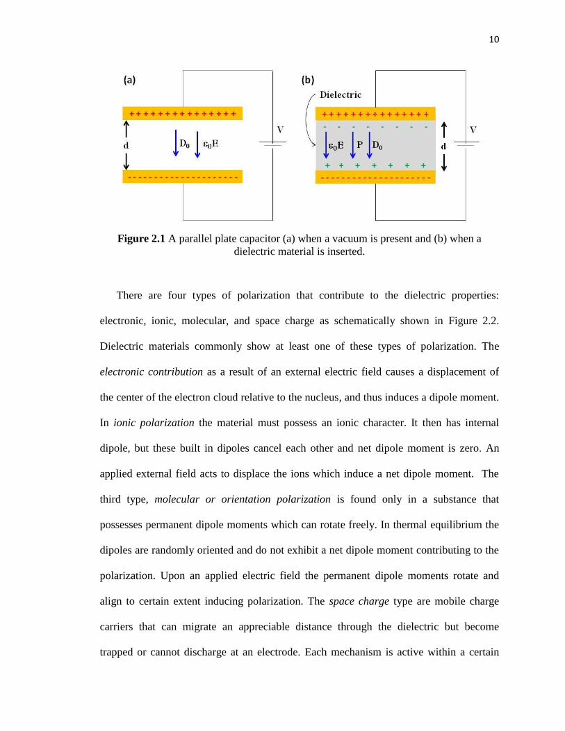
10
Figure 2.1 A parallel plate capacitor (a) when a vacuum is present and (b) when a
dielectric material is inserted.
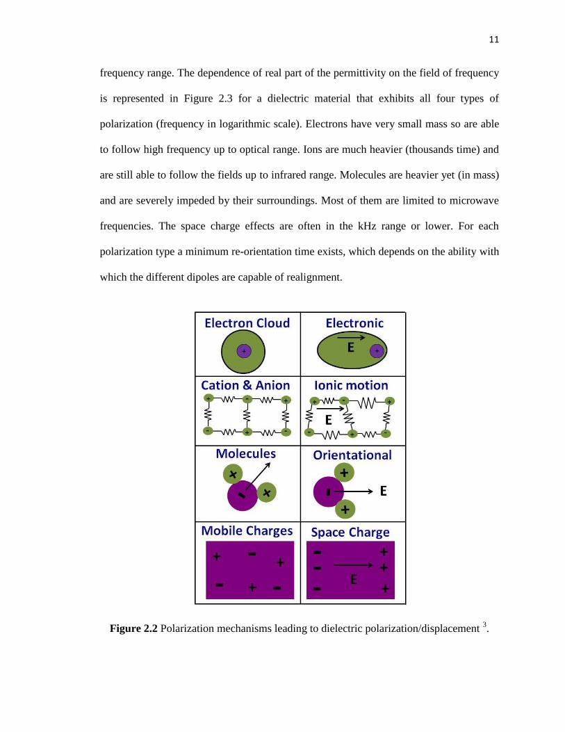
There are four types of polarization that contribute to the dielectric properties:
electronic, ionic, molecular, and space charge as schematically shown in Figure 2.2.
Dielectric materials commonly show at least one of these types of polarization. The
electronic contribution as a result of an external electric field causes a displacement of
the center of the electron cloud relative to the nucleus, and thus induces a dipole moment.
In ionic polarization the material must possess an ionic character. It then has internal
dipole, but these built in dipoles cancel each other and net dipole moment is zero. An
applied external field acts to displace the ions which induce a net dipole moment. The
third type, molecular or orientation polarization is found only in a substance that
possesses permanent dipole moments which can rotate freely. In thermal equilibrium the
dipoles are randomly oriented and do not exhibit a net dipole moment contributing to the
polarization. Upon an applied electric field the permanent dipole moments rotate and
align to certain extent inducing polarization. The space charge type are mobile charge
carriers that can migrate an appreciable distance through the dielectric but become
trapped or cannot discharge at an electrode. Each mechanism is active within a certain
11
frequency range. The dependence of real part of the permittivity on the field of frequency
is represented in Figure 2.3 for a dielectric material that exhibits all four types of
polarization (frequency in logarithmic scale). Electrons have very small mass so are able
to follow high frequency up to optical range. Ions are much heavier (thousands time) and
are still able to follow the fields up to infrared range. Molecules are heavier yet (in mass)
and are severely impeded by their surroundings. Most of them are limited to microwave
frequencies. The space charge effects are often in the kHz range or lower. For each
polarization type a minimum re-orientation time exists, which depends on the ability with
which the different dipoles are capable of realignment.
Figure 2.2 Polarization mechanisms leading to dielectric polarization/displacement 3.

12
Figure 2.3 Variation of dielectric constant with frequency of alternating electric field.
Electronic, ionic, orientation and space charge contributions to the dielectric constant are
indicated 1,4
.
Dielectrics materials are classified in two major categories: non ferroelectric
(paraelectric or normal dielectric) and ferroelectric. The non ferroelectric category may
be divided into three classes: Non polar materials, polar materials and dipolar materials.
In this category, the polarization is caused by an electric field. For the first class of non
ferroelectric the electric field can only produce elastic displacement of the electron clouds
so they only have electronic polarization. Such materials are referred as elemental
materials which consist of a single atom. For this category the absorption occurs at the
resonance frequency which is in the visible-ultraviolet region. In the second class, an

13
electric field will cause elastic displacement of the electron cloud and elastic
displacement of the positions of ions. Such materials exhibit both electronic and ionic
polarization. The absorption occurs at two different resonant frequencies: (1) optical
frequency region and (2) infrared region which corresponds to the electronic and ionic
polarization respectively. The third class has three types of polarization electronic, ionic
and orientational 5. The second category of ferroelectric dielectrics is going to be
discussed in the next session.
2.3 Piezoelectricity
Structural symmetry of crystal depends on its lattice structure which is described by
Bravais unit cell of the crystal. There are only thirty two macroscopic symmetry types
and can be classified as follows: centrosymmetry and non-centrosymmetry. The first type
with center symmetry includes eleven point groups. The other twenty one point groups
among the thirty two groups do not have centrosymmetry. All non centrosymmetry point
groups except the point group 432 exhibit piezoelectric effect. The piezoelectric effect
was discovered by Jacques Curie and Pierre Currie in 1880. Piezoelectricity is the electric
charge accumulated in response to an applied mechanical stress. Such phenomenon is
known as the direct effect. When an electric field is applied and the polarization cause a
change in the shape or dimensions it’s called the converse effect 6. The equations that
described the piezoelectric effect in regard of the elastic and electric properties are in a
general form:
(2.5)
(2.6)
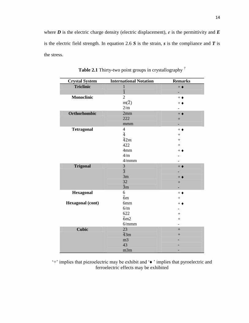
14
where D is the electric charge density (electric displacement), ɛ is the permittivity and E
is the electric field strength. In equation 2.6 S is the strain, s is the compliance and T is
the stress.
Table 2.1 Thirty-two point groups in crystallography 7
Crystal System International Notation Remarks
Triclinic 1
+
-
Monoclinic 2
m(
2/m
+
+
-
Orthorhombic 2mm
222
mmm
+
+
-
Tetragonal 4
422
4mm
4/m
4/mmm
+
+
+
+
+
-
-
Trigonal 3
3m
32
m
+
-
+
+
-
Hexagonal
Hexagonal (cont)
6
m
6mm
6/m
622
m2
6/mmm
+
+
+
-
+
+
-
Cubic 23
3m
m3
43
m3m
+
+
-
-
-
‘+’ implies that piezoelectric may be exhibit and ‘’ implies that pyroelectric and
ferroelectric effects may be exhibited
15
Piezoelectric materials are utilized in transducers which are devices that convert an
electrical signal into a mechanical strain or vice versa. The symmetry of a crystal affects
the properties of a material such as dielectric, elastic, piezoelectric, ferroelectric and
nonlinear optical properties.
2.4 Ferroelectric materials
The group of dielectric called ferroelectric exhibit spontaneous polarization (Ps) in the
absence of an electric field. The electric dipoles are not randomly placed but interact in
such a way as to align themselves even without an external field. A distinguished feature
of ferroelectrics is that the spontaneous polarization can be reversed by strong applied
electric field in the opposite direction. Among the twenty point groups that exhibit
piezoelectricity there are ten point groups that have one unique direction axes and thus
possesses spontaneous polarization. A material that exhibit spontaneous polarization is
composed of negative and positive ions. In certain temperature range the ions are in
equilibrium and the center of the positive charge does not coincide with the center of the
negative charge at this point the free energy of the crystal is minimum. There are
different types of ferroelectric materials according to their crystallization such as
perovskite, bronze-tungsten, and bismuth layer structure. The first one of the three is the
best known material used for many applications. For example Figure 2.4 shows the
crystal structure for perovskite ferroelectric barium titanate (BaTiO3).
An important characteristic of ferroelectric is the transition temperature called Curie
temperature, TC. When the temperature decreases through TC the ferroelectric crystal
experience a transition from a paraelectric phase to a ferroelectric phase. When the
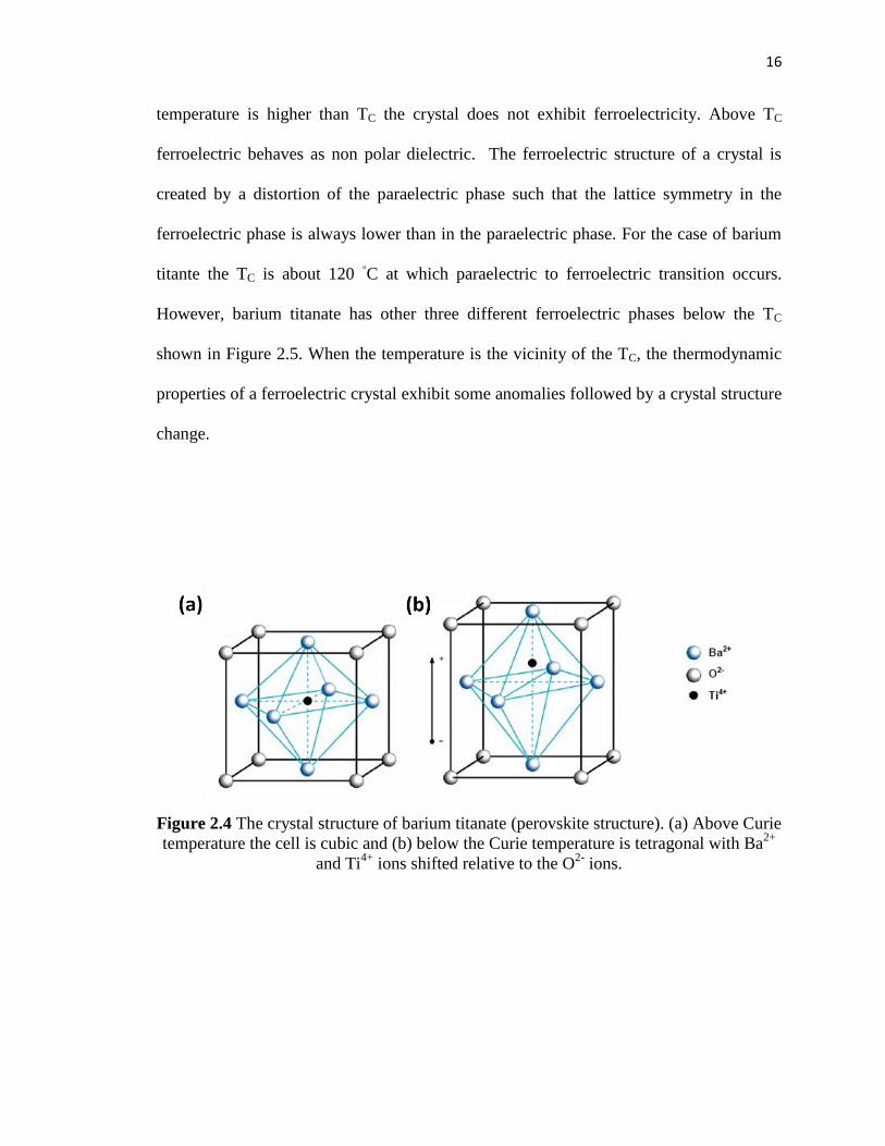
16
temperature is higher than TC the crystal does not exhibit ferroelectricity. Above TC
ferroelectric behaves as non polar dielectric. The ferroelectric structure of a crystal is
created by a distortion of the paraelectric phase such that the lattice symmetry in the
ferroelectric phase is always lower than in the paraelectric phase. For the case of barium
titante the TC is about 120 ◦C at which paraelectric to ferroelectric transition occurs.
However, barium titanate has other three different ferroelectric phases below the TC
shown in Figure 2.5. When the temperature is the vicinity of the TC, the thermodynamic
properties of a ferroelectric crystal exhibit some anomalies followed by a crystal structure
change.
Figure 2.4 The crystal structure of barium titanate (perovskite structure). (a) Above Curie
temperature the cell is cubic and (b) below the Curie temperature is tetragonal with Ba2+
and Ti4+
ions shifted relative to the O2-
ions.

17
Figure 2.5 Temperature dependence of the dielectric constant in barium titanate 8.
Figure 2.6 Barium titanate phase transition below TC 4.

18
The temperature dependence of the dielectric constant above the TC can be described by
the Curie-Weiss law 3,7
:
(2.7)
where C is the Curie-Weiss constant and Ɵ0 the Curie-Weiss temperature. Ɵ0 is different
from the Curie point. In the case of a first order transition, Ɵ0 < ƟC, while for second
order transition Ɵ0 = ƟC. Usually the term ɛ0 can be neglected because it is much smaller
than C/(Ɵ-Ɵ0) when Ɵ is near Ɵ0.
Other characteristic of ferroelectrics is the hysteresis loop. The polarization is double-
valued function of the applied electric field. At low applied electric field a liner
relationship between the polarization and electric field is observed, because the electric
field is not high enough to switch any domain and the material will behave as a normal
dielectric. As the electric field increases a number of domains will be switch in one
direction, and the polarization will increase rapidly until all the domains are aligned. This
state is called saturation. When the electric field is decrease the polarization will also
decrease but does not return to zero. Once the electric field reach zero some of the
domains will remain aligned, and a remnant polarization is observed. In order to remove
the remnant polarization an electric field in the opposite direction (negative) is applied.
Further increase of the electric field on the opposite direction (negative) will cause an
alignment of the domains in the opposite direction. The electric field required to reduce
the polarization to zero is called the coercive field. The relation between polarization and
electric field is represented by a hysteresis loop shown in Figure 2.7. The area within the
loop is a measure of the energy to twice reverse the polarization 2. The spontaneous

19
polarization is equal to the saturation value of the electric displacement extrapolated to
zero field. The remnant polarization is different than the spontaneous polarization if
reverse nucleation occurs before the applied field reverses. This can happen in the
presence of an internal/external stresses or if the free charges cannot reach the new
equilibrium distribution during each half of the hysteresis loop. When doing this type of
measurements special caution must be take into account. Firstly, the loop gives only
measure of the switchable portion of the spontaneous polarization. Secondly, ferroelectric
hysteresis loop can easily be confused with non-linear dielectric loss. Errors in the
characterization of spontaneous polarization and even incorrect identification of
ferroelectrics can be as a result of the non-linear contributions to the displacement 2.
Figure 2.7 Typical hysteresis loop 7.

20
In a ferroelectric is likely that the electric dipoles aligned only in certain regions of
different polarization. Each of these regions is called domains. A domain is a
homogenous ferroelectric region in which all the dipoles moments in adjacent unit cell
have the same orientation. There are several types of domains, and the two most common
are: (1) 90◦ wall in which polarization vectors in adjacent domains at right angles and (2)
180◦ in which polarization vectors in adjacent domains are anti-parallel. Then the net
polarization depends on the difference of the two domains orientations. If the volumes of
the domains are equal then there is not a net polarization. The interface between those
domains are called domain wall. The domain wall separates regions where the
polarization changes. They have a width of 0.2 to 0.3 nm but this varies with crystal and
temperature.
Figure 2.8 (a) ionic displacement in two 180◦ ferroelectric domains, (b) domain structure
is showing several 180◦ domains of different sizes and (c) 180
◦ domain wall with a width
of ~ 0.2 - 0.3 nm 4.

21
2.5 Ferromagnetism
Analogous to ferroelectricity, ferromagnetism has a spontaneous magnetic moment in
zero applied magnetic fields. The electron spins and magnetic moments are arranged in a
regular manner. All of the spin arrangements sketched in Figure 2.9 except the simple
antiferromagnet have a spontaneous magnetic moment, called saturation moment. The
magnetization is defined as the magnetic moment per unit volume. Similar to
ferroelectric materials, ferromagnetic posses regions magnetized in different directions
called domains. The magnetization refers to the value within a domain. The Curie
temperature, TC is the temperature above which spontaneous magnetization disappears.
Figure 2.9 Order arrangements of electron spins 9.
A feature of ferromagnetic materials is the hysteresis loop which can be understood
similar to a ferroelectric hysteresis loop through the concept of domains (magnetic). The
motion of the domains and the re-orientation of the domains directions is not totally
reversible evidence with a remnant magnetization. When the applied magnetic field is
decrease (reverse) to the initial value, the domains do not return completely to their
original position but retain some “memory” of their alignment. This memory leads to one
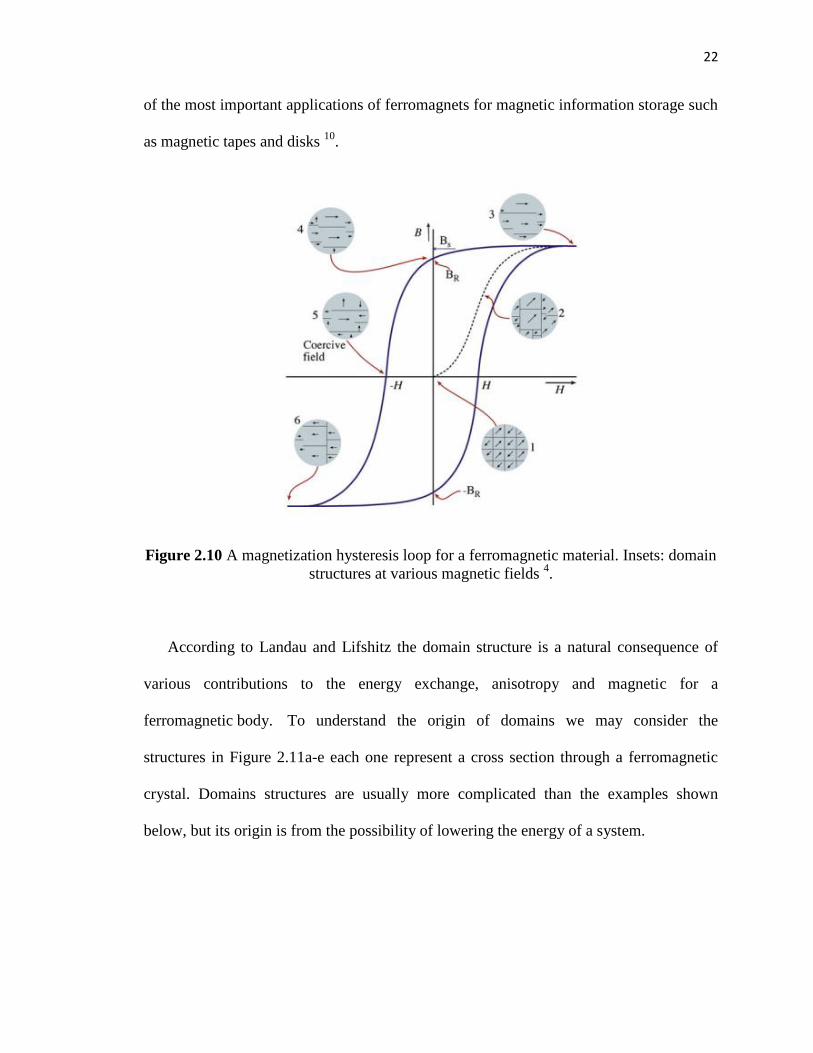
22
of the most important applications of ferromagnets for magnetic information storage such
as magnetic tapes and disks 10
.
Figure 2.10 A magnetization hysteresis loop for a ferromagnetic material. Insets: domain
structures at various magnetic fields 4.
According to Landau and Lifshitz the domain structure is a natural consequence of
various contributions to the energy exchange, anisotropy and magnetic for a
ferromagnetic body. To understand the origin of domains we may consider the
structures in Figure 2.11a-e each one represent a cross section through a ferromagnetic
crystal. Domains structures are usually more complicated than the examples shown
below, but its origin is from the possibility of lowering the energy of a system.
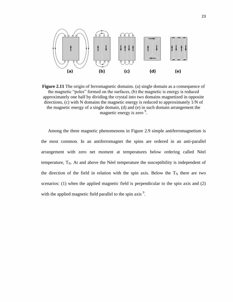
23
Figure 2.11 The origin of ferromagnetic domains. (a) single domain as a consequence of
the magnetic “poles” formed on the surfaces, (b) the magnetic is energy is reduced
approximately one half by dividing the crystal into two domains magnetized in opposite
directions, (c) with N domains the magnetic energy is reduced to approximately 1/N of
the magnetic energy of a single domain, (d) and (e) in such domain arrangement the
magnetic energy is zero 9.
Among the three magnetic phenomenons in Figure 2.9 simple antiferromagnetism is
the most common. In an antiferromagnet the spins are ordered in an anti-parallel
arrangement with zero net moment at temperatures below ordering called Néel
temperature, TN. At and above the Néel temperature the susceptibility is independent of
the direction of the field in relation with the spin axis. Below the TN there are two
scenarios: (1) when the applied magnetic field is perpendicular to the spin axis and (2)
with the applied magnetic field parallel to the spin axis 9.

24
2.6 Multiferroic phenomenon and materials
Multiferroic combines any two or more of the primary ferroic orderings in the sample
phase such as: ferroelectriccity, feroelasticity, and ferromagnetism (or any kind of
magnetic order). However, current fashion applies the term multiferroic primarily to
materials that exhibit simultaneous ferroelectric or ferromagnetic order. The most
attractive aspect of multiferroic is the magnetoelectric coupling. In the magnetoelectric
coupling a ferroic property is modified or controlled using its associated field (magnetic
field modify magnetization and electric field modify polarization). In a multiferroic a
magnetic field can tune the electric polarization and vice versa the electric field can tune
the magnetization. In terms of the applications, the ability to use electric field to control
the magnetism is particularly interesting because it could lead to smaller and more
efficient device for magnetic technologies.
Figure 2.12 Multiferroics combined the properties of ferroelectrics and magnets 11
.
This phenomenon results in fascinating from a physics stand point because the
mechanism to observe ferroelectricity and ferromagnetism is mutually exclusive. The
conventional mechanism in ferroelectric requires formally empty d orbitals while the

25
formation of magnetic moment results from partially filled d orbitals. Also considering
that polarization is represented by a polar vector and magnetization by an axial vector
they have different symmetry properties; and is not clear that one should be addressed by
the other associated field. Another restriction is that in order for a ferroelectric to keep a
polarization, the material must be a robust insulator. However, most magnetic materials
are conducting metals. In conventional ferroelectrics (single phase), the polarization
arises when non magnetic cations shift away from the center of the surroundings anions.
In other hand for magnetic materials, the magnetic cations tend to sit exactly at the center
of the surroundings anions. In principle ferroelectricity and magnetism coupling could be
achieve through an alternative non d electron mechanism for magnetism or an alternative
mechanism for ferroelectricity. Presently in practice only the latter route has been
pursued but there are also other possibilities summarized in the Table 2.2.
To better understand the basic phenomena and appreciate the main achievements and
remaining problems it’s necessary to classify multiferroics by the microscopic
mechanism that determines their properties. Generally speaking there are two groups of
multiferroics 11
. The first group which is called type I multiferroics, contains those
material where ferroelectricity and magnetism have different source and are independent
of one another, but there is still some coupling between them. In this group
ferroelectricity appears at higher temperature compared to magnetism and polarization is
large in the order of 10 – 100 C.cm-2
. Unfortunately the coupling in type I is usually
weak. The challenge in this group is to maintain all their positive features but enhance the
coupling. The second group which is called type II multiferroics magnetism causes
ferroelectricity implying a high coupling between the two. However, in this case different
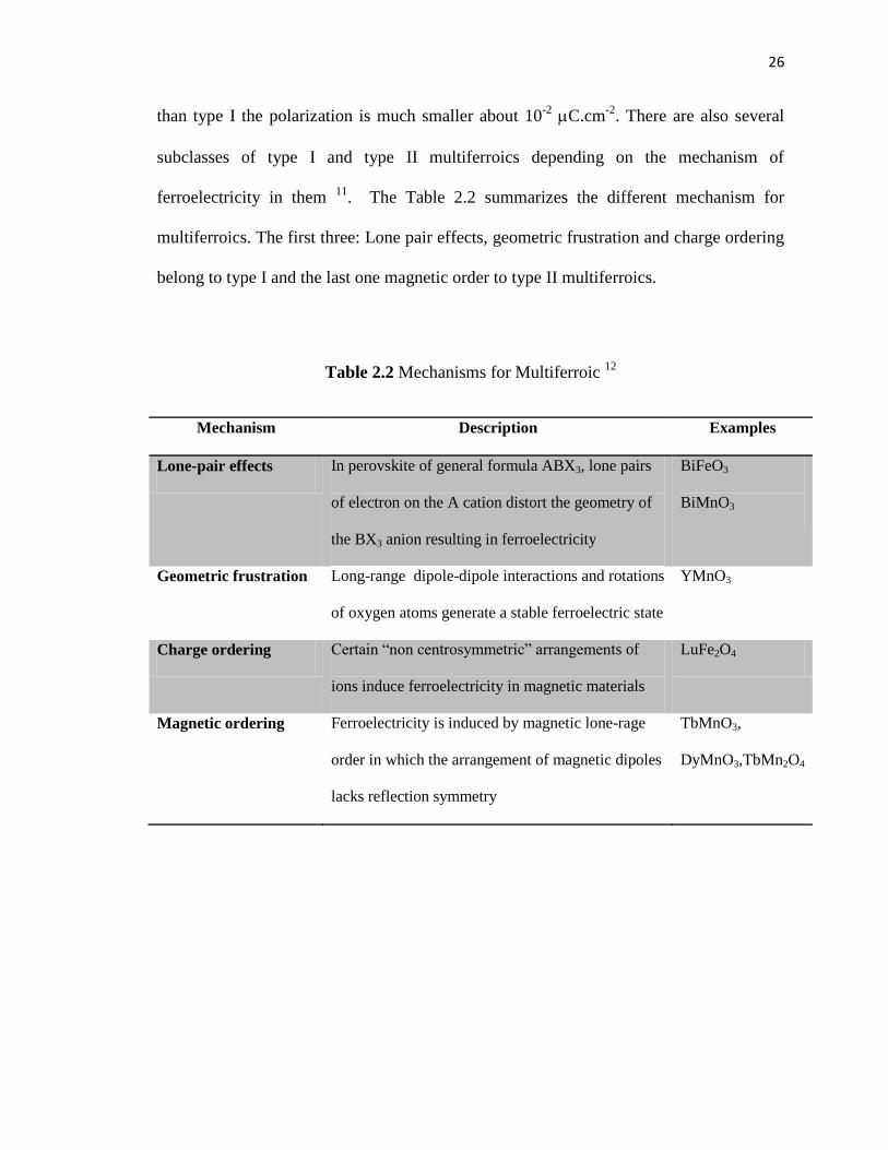
26
than type I the polarization is much smaller about 10-2
C.cm-2
. There are also several
subclasses of type I and type II multiferroics depending on the mechanism of
ferroelectricity in them 11
. The Table 2.2 summarizes the different mechanism for
multiferroics. The first three: Lone pair effects, geometric frustration and charge ordering
belong to type I and the last one magnetic order to type II multiferroics.
Table 2.2 Mechanisms for Multiferroic 12
Mechanism Description Examples
Lone-pair effects In perovskite of general formula ABX3, lone pairs
of electron on the A cation distort the geometry of
the BX3 anion resulting in ferroelectricity
BiFeO3
BiMnO3
Geometric frustration Long-range dipole-dipole interactions and rotations
of oxygen atoms generate a stable ferroelectric state
YMnO3
Charge ordering Certain “non centrosymmetric” arrangements of
ions induce ferroelectricity in magnetic materials
LuFe2O4
Magnetic ordering Ferroelectricity is induced by magnetic lone-rage
order in which the arrangement of magnetic dipoles
lacks reflection symmetry
TbMnO3,
DyMnO3,TbMn2O4

27
2.7 Semiconductor materials
Conductors are generally substances which have the property to pass different types
of energy. The conductivity of metals is based on the free electrons due to the metal
bonding. For an electron to become free it must be excited to one of the empty and
available energy states above the Fermi Energy EF. According to energy band structure
for metals shown in Figure 2.13a there are vacant energy states adjacent to the highest
filled state. This small energy is required to excite an electron into the low empty state.
The insulators do not possess free charge carriers and thus are non conductive. Empty
spaces adjacent to the top of the filled valence band are not available. In order for an
electron to become free, it must be promoted across the energy band gap into empty
spaces at the bottom of the conduction band. This is only possibly by providing to an
electron the energy which is approximately equal to the Eg (difference in energy between
the conduction and valence band).
A semiconductor is a type of material that has an electrical resistance which is
between electrical resistance typical of metals and insulators. The main difference
between a semiconductor and an insulator is that the semiconductor possesses a much
smaller energy band gap Eg, between the top of the highest filled band (called the valence
band), and the bottom of the vacant band just above it (called the conduction band) 13
.
The conductivity of a semiconductor is not as high as that of a metal nevertheless they
have unique features that make them useful for special applications. Semiconductors can
be classified in two groups: elemental semiconductor materials found in group IV of the
periodic table and the compound semiconductor materials, most of which are formed
from combinations of group III and group V elements 13
.

28
Figure 2.13 The energy band structure for (a) metal, (b) insulator and
(c) semiconductor 13,14
.
The electrical properties of semiconductors are sensitive to the presence of minimum
amount of impurities leading to two types of electrical behavior. First, intrinsic
semiconductors are those in which electrical behavior depend on the electronic structure
inherent in the pure material. Second, extrinsic semiconductors are those in which the
electrical behavior is influenced by the presence of impurity atoms.
The intrinsic semiconductor is characterized with an energy band structure shown in
Figure 2.13c in which the valence band is filled and for every electron excited into the
conduction band there is vacant electron state in the valence band called a hole. A hole is
considered to have the same magnitude as an electron but with an opposite sign. Thus, in
presence of an electric field both electrons and holes move in opposite directions.
Practically all commercial semiconductors are extrinsic. When the density of electrons is
greater than the density of holes, the semiconductor is considered as n type; donor
impurity atoms have been added. When the density of holes is greater than the density of
electrons, the semiconductor is p type; acceptor impurity atoms have been added 15
.
Considering an n type semiconductor a silicon (Si) atom has four electrons, each of
which is covalently bonded with one of four adjacent Si atoms. If an impurity atom with

29
a valence of five is added as substitutional impurity only four of the five electrons of
dopant can participate in the bonding because there only four possible bonds with
neighbor atom. The extra non-bonding free electron is loosely bound near the region of
the impurity atom by a weak electrostatic attraction. For each of the weakly bound
impurities there is an energy state which is located within the forbidden band gap just
below the conduction band. The electron binding energy is the energy required to excited
one electron from this impurity energy state into the conduction band. Each excitation
step donates a single electron to the conduction band – an impurity of these types is
called donor. Since each donor is promoted from an impurity level there is no a
corresponding hole left behind in the valence band. The electrons are majority carriers by
their concentration and holes on the other hands are minority charge carries. An opposite
effect is produced by adding a trivalent substitutional impurity such as aluminum, boron
and gallium from the Group IIIA. One of the covalent bonds around each of the atoms is
deficient of an electron such a deficiency may be view as a hole which is weakly bound
to the impurity atom. In this case each impurity atom of this type introduces an energy
level just above the valence band. An impurity of this nature is called an acceptor,
because it is able to accept and electron from the valence band leaving a hole.
30
Figure 2.14 Extrinsic semiconductor (a) n-type: an impurity atom such as phosphorus
with five valence electrons may substitute for a silicon atom resulting in an extra bonding
electron,(b) n-type band diagram, (c) p-type: an impurity atom such as boron with three
valence electrons may substitute for silicon atom resulting in a deficiency of a one
valence electron, and (d) p-type band diagram: 1.
The conductivity of a semiconductor material besides to being affect it by the
concentration of impurities is also a function of the charge carrier mobilities. The career
mobility is the ease with which electron and holes are transported through it. The
magnitude of electron and holes mobilities is influenced by the same crystalline defects
that are responsible for the scattering of electrons in metals: thermal vibrations and
impurity atoms.
31
The unique electrical properties of semiconductor allow their use in devices to
perform different functions. Diodes and transistors are two familiar examples. Some
advantages of implementing semiconductor materials in electronic technologies are small
size, lower power consumption, and no warm up time.
One of the first example diodes or rectifiers is a device that permits the flow of
current in one direction but not in the other. A rectifier transforms an alternative current
into a direct current. The rectifying junction is constructed from a single piece of
semiconductor that is doped to be n type in one side and p type in the other side. Before
applying any potential as discussed previously the n type side will be dominated by
electrons carriers and the p type with holes. An external field could be applied across the
p-n junction with two different polarities: forward bias or reverse bias. In a forward bias
the positive terminal is connected to the p-side and negative to the n-side, the opposite
polarity is referred as reverse bias 1. The response of carriers to different polarities is
shown in Figure 2.15. In the forward bias the electrons and holes are attracted to the
junction area once they encounter continuously recombine. For these bias large number
of carriers flow across the semiconductor junction as evidenced by an appreciable current
and low resistivity. Oppositely, for reverse bias the carriers (electrons and holes) are
pulling away from the junction leaving the junction region free of mobile careers and
recombination will not occur. Thus, there is no flow of current and the junction become
highly insulative.

32
Figure 2.15 For a p-n rectifying junction representation of electron and hole distributions
for (a) non electrical potential, (b) forward bias and (c) reverse bias 1.
Another example is the transistor which is an important semiconducting device in
microelectronics circuitry. Transistor has two primary main functions: amplify an
electrical signal and serve as switching devices for the processing and storage of
information. A field effect transistor (FET) is a transistor that used an electric field (or the

33
lack of voltage) to control the shape and therefore the conductivity of a channel of one
type of charge carrier in a semiconductor material 2. Field effect transistors can be
majority charge carriers devices in which the current is mostly due to majority carriers it
can also be a minority charge carrier device in which the current is mainly because a
flow of minority carriers. The device consists of a channel through which charge carriers
(electrons or holes) flow from the source to the drain. The source and drain are part of the
device architecture. They are conductors and are connected to the semiconductor material
through ohmic contact. The conductivity of the channel depends on the potential applied
across the gate and source terminals. The gate allows electrons to flow or block their
passage by opening and closing the channel between the source and drain. In summary
the FET’s three terminals are 13
.
1. Source (S) through which the carriers enter the channel
2. Drain (D) through which carriers leave the channel
3. Gate (G) terminal that modulates the channel conductivity and controls the
current coming out of the drain terminal
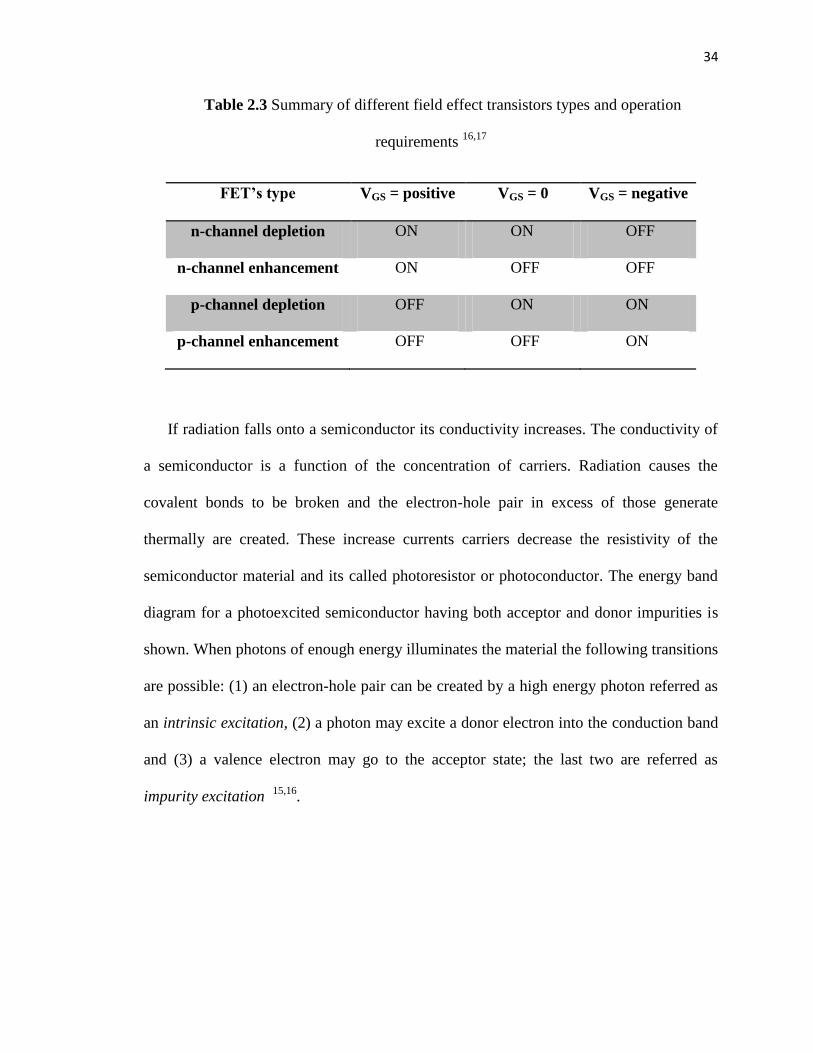
There are four types of FET’s: n-channel enhancement or depletion mode and p-
channel enhancement or depletion mode. The n-channel and p-channel as explain
previously is related to the density of electrons and holes in the semiconductor material.
In the enhancement mode the transistor requires a voltage between gate and source (VGS)
to switch the device “ON” while the depletion mode requires a VGS to switch the device
“OFF”. The enhancement mode is equivalent to a “Normally Open” switch while the
depletion mode is equivalent to a “Normally Closed” switch.
34
Table 2.3 Summary of different field effect transistors types and operation
requirements 16,17
FET’s type VGS = positive VGS = 0 VGS = negative
n-channel depletion ON ON OFF
n-channel enhancement ON OFF OFF
p-channel depletion OFF ON ON
p-channel enhancement OFF OFF ON
If radiation falls onto a semiconductor its conductivity increases. The conductivity of
a semiconductor is a function of the concentration of carriers. Radiation causes the
covalent bonds to be broken and the electron-hole pair in excess of those generate
thermally are created. These increase currents carriers decrease the resistivity of the
semiconductor material and its called photoresistor or photoconductor. The energy band
diagram for a photoexcited semiconductor having both acceptor and donor impurities is
shown. When photons of enough energy illuminates the material the following transitions
are possible: (1) an electron-hole pair can be created by a high energy photon referred as
an intrinsic excitation, (2) a photon may excite a donor electron into the conduction band
and (3) a valence electron may go to the acceptor state; the last two are referred as
impurity excitation 15,16
.
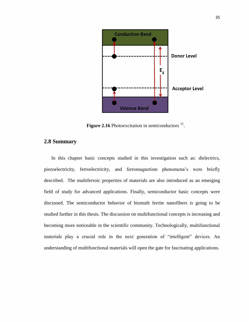
35
Figure 2.16 Photoexcitation in semiconductors 15
.
2.8 Summary
In this chapter basic concepts studied in this investigation such as: dielectrics,
piezoelectricity, ferroelectricity, and ferromagnetism phenomena’s were briefly
described. The multiferroic properties of materials are also introduced as an emerging
field of study for advanced applications. Finally, semiconductor basic concepts were
discussed. The semiconductor behavior of bismuth ferrite nanofibers is going to be
studied further in this thesis. The discussion on multifunctional concepts is increasing and
becoming more noticeable in the scientific community. Technologically, multifunctional
materials play a crucial role in the next generation of “intelligent” devices. An
understanding of multifunctional materials will open the gate for fascinating applications.
36
2.9 References
1. Callister, W. D. Materials Science And Engineering: An Introduction. (John
Wiley & Sons, 2007).
2. Lines, M. E. & Glass, A. M. Principles and applications of ferroelectrics and
related materials. (Clarendon Press, 1977).
3. Newnham, R. E. Properties of Materials : Anisotropy, Symmetry, Structure:
Anisotropy, Symmetry, Structure. (Oxford University Press, 2004).
4. Carter, C. B. & Norton, M. G. Ceramic Materials: Science and Engineering.
(Springer, 2007).
5. Kao, K.-C. Dielectric Phenomena in Solids: With Emphasis on Physical Concepts
of Electronic Processes. (Academic Press, 2004).
6. Piezoelectricity. Wikipedia, the free encyclopedia (2014). at
<http://en.wikipedia.org/w/index.php?title=Piezoelectricity&oldid=612134483>
7. Xu, Y. Ferroelectric Materials and Their Applications. (North-Holland, 1991).
8. Merz, W. J. The Electrical and Optical Behavior of Barium Priderite Single
Domain Crystals. Phys. Rev. 76, 1221–1225
9. Kittel, C. Introduction to Solid State Physics. (Wiley, 2005).
10. Halliday, D. Fundamentals of Physics Extended, Eighth Edition Binder Ready
Version. (John Wiley & Sons Canada, Limited, 2007).
11. Khomskii, D. Classifying multiferroics: Mechanisms and effects. Physics 2, 20
(2009).
12. Ramesh, R. Materials science: Emerging routes to multiferroics. Nature 461,
1218–1219 (2009).
13. Neamen, D. A. Semiconductor Physics And Devices: Basic Principles. (McGraw-
Hill, 2011).
14. Laube, P. SemiconductorTechnology from A to Z. at
<http://www.halbleiter.org/en/fundamentals/conductors/>
15. Millman, J., Halkias, C. & Jit, S. Electronic Devices and Circuits. (McGraw-Hill
Education (India) Pvt Limited, 2008).
16. Amos, S. W. & James, M. Principles of Transistor Circuits. (Newnes, 2000).
17. MOSFET and Metal Oxide Semiconductor Tutorial. Basic Electronics Tutorials
at <http://www.electronics-tutorials.ws/transistor/tran_6.html>

37
3 Literature Review
3.1 Introduction
Bismuth ferrite; BiFeO3 (BFO), is a multiferroic material that exhibit ferroelectricity
and antiferromagnetism. It is perhaps the only material that exhibit multiferroicity at
room temperature. Bulk properties of BFO have been extensively studied but its
electromechanical properties are hindered due to high leakage problems. This is mostly
due to the difficulties in materials processing and non stoichiometric single phase
bismuth ferrite 1,2
. Further research in the area of thin films resulted in enhanced
fabrication methods and outstanding properties of epitaxial BFO heterostructure with
high remnant polarization 3 establishing a renaissance among the scientific community.
Such outcome opened the gate for a great deal interest and efforts to resume the
investigation in the area.
Recently, it has been reported the size effect has a very strong influence in the
magnetic properties of bismuth ferrite 4,5
. As a result there has been quick growth in the
fabrication and characterization of BFO nanostructures such as cubes 6, fibers
7,8, rods
9,
tubes 4, and crystals
8.
Bismuth ferrite is also an attractive material for photoconduction applications because
of its distinctive optical band gap compared to other ferroelectric materials. BFO
possesses a band gap of 2.7 eV which falls in the visible range and absorbs significant
amount of the light spectrum 10,11
.
This chapter attempts to summarize the characteristics, fabrication, and properties of
BFO thin films and nanostructures.

38
3.2 Bismuth ferrite
The study of BFO started in 1960 by Smolenskii et al. but difficulties in the growth
of single crystals resulting in high conductivity prevent the material for further
investigation and practical applications 12
. In 1967, Achenbach and colleagues succeed in
the preparation of single phase polycrystalline BFO by removing unwanted phases by
watching the material with nitric acid 13
. In 1970, the polarization for bulk BFO was
reported to be 6.1 C.cm-2 14
. Precise x-ray diffraction studies in 1990 on monodomain
single crystal revealed BiFeO3 structure 15
. In 2003, the discovery of a large remnant
polarization (15 times larger) along with strong ferromagnetism 3 of thin films marked
the beginning of a new age for bismuth ferrite as a multiferroic material.
Figure 3.1 (a) Hysteresis loop measured at 15 kHz showing high remnant polarization
~55 C.cm-2
, and (b) magnetic hysteresis loop for 70 nm BFO film with an appreciable
saturation magnetization of 150 emu.cm-3
, and a coercive field of 200 Oe. NOTE: The
in-plane loop is shown in blue, and the out-of-plane loop is in red.3

39
At room temperature bulk bismuth ferrite possesses a simple ABO3 rhombohedral
distorted perovskite structure with space group R3c. The unit cell can be described as
pseudo-cubic, rhomobohedral or hexagonal where [111]pc, || [111]rh, || [001]hex. The
lattice constant determined by Kubel and Schimid are: apc = 3.965 Å, αpc = 89.35 ◦ for the
pseudocubic unit cell, arh = 5.6343 Å, αrh = 59.348 ◦ in the rhombohedral unit cell and
ahex = 5.578 Å, chex = 13.868 Å for the hexagonal unit cell 15
. When grown as a thin film,
it has been shown that the structure could be monoclinic or tetragonal depending upon the
strain imposed by the substrate 16,17
and level of mismatching.
Figure 3.2 Perovskite crystal structure of bulk BiFeO3 18
.

40
From a structural point of view an important parameter is the rotation angle of the
oxygen octahedra. Equation 3.1 is used to measure how well the ions fit into the
perovskite unit cell.
(3.1)
where r is the ionic radii of the respective ion and l is the length of the octahedral edge.
This parameter is analogous to the tolerance factor as shown Equation 3.2. Using the
Shannon atomic radii the tolerance for BiFeO3 is equal to 0.88.
(3.2)
Bismuth ferrite shows spontaneous polarization along one of the eight pseudo-cubic
[111] axes with a Curie temperature of 830 ◦C. Calculated spontaneous polarization is
predicted to be about 100-150 C.cm-2
and has been confirmed in thin films 3. The
polarization in BiFeO3 is caused by the lone pair (s2 orbital) of Bi
3+, so mostly from the
A-site while the magnetization comes from the B-site (Fe3+
). Bulk BFO exhibits G-type,
antiferromagnetism with Néel temperature of 380 ◦C. In the G-type both the intraplane
and interplane are antiferromagnetic; each Fe3+
with spin up is surrounded by six of the
nearest Fe neighbors with spin down. The antiferromagnetic structure has a modulation
vector with a periodicity of λ = 0.62 - 0.64 nm. There is a small canting of Fe magnetic
moment leading to a net magnetization of 5 emu.cm-3
and some thin film exhibit larger
saturation magnetization exceeding 70 emu.cm-3
3. However, the origin for such a high
magnetization value in thin films is not well defined and is cause of arguments.
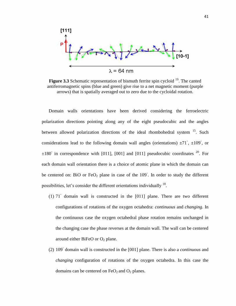
41
Figure 3.3 Schematic representation of bismuth ferrite spin cycloid 19
. The canted
antiferromagnetic spins (blue and green) give rise to a net magnetic moment (purple
arrows) that is spatially averaged out to zero due to the cycloidal rotation.
Domain walls orientations have been derived considering the ferroelectric
polarization directions pointing along any of the eight pseudocubic and the angles
between allowed polarization directions of the ideal rhombohedral system 15
. Such
considerations lead to the following domain wall angles (orientations) ±71◦, ±109
◦, or
±180◦ in correspondence with [011], [001] and [011] pseudocubic coordinates
20. For
each domain wall orientation there is a choice of atomic plane in which the domain can
be centered on: BiO or FeO2 plane in case of the 109◦. In order to study the different
possibilities, let’s consider the different orientations individually 18
.
(1) 71◦ domain wall is constructed in the [011] plane. There are two different
configurations of rotations of the oxygen octahedra: continuous and changing. In
the continuous case the oxygen octahedral phase rotation remains unchanged in
the changing case the phase reverses at the domain wall. The wall can be centered
around either BiFeO or O2 plane.
(2) 109◦ domain wall is constructed in the [001] plane. There is also a continuous and
changing configuration of rotations of the oxygen octahedra. In this case the
domains can be centered on FeO2 and O2 planes.

42
(3) 180◦ domain wall constructed in the [0 ] plane. Again, two octahedral tilt have
been explored. Similar to the 71◦ domain wall is not possible to distinguish
between the BiFeO and O2 centered domain walls.
The domain walls play an important role in the electronic properties because of their
size, local symmetry, individual properties, and due to the fact that their location can be
controlled. In the case of BFO one of the unique properties within or in the domain wall
for different walls orientations is the change in conductivity. Ramesh and coworkers have
reported that certain domain walls of BFO are much more conductive than the domains
21. The conductivity of the walls is related to the type of domains they are separated.
Epitaxial BFO thin films carefully grown on SrRuO3 (50 nm) as buffer layer bottom
electrode and SrTiO3 (100) oriented was used to study the conductivity of the domain
walls. The films were grown by laser molecular beam epitaxy technique and ferroelectric
domains were imaged by piezoelectric force microscopy (PFM). In order to study the
three different types of domains characteristics of BFO (71◦, 109
◦ and 180
◦), controlled
ferroelectric domains pattern were written using a PFM by applying a DC voltage. The
presence of all three types of domains was confirmed by PFM imaging. Conductive
atomic force microscope (c-AFM) shows the occurrence of conduction at 109◦ and 180
◦
walls but not in 71◦ walls. The authors argue two reasons for the observed conductivity
of the domains walls: (1) the polarization normal to the domain wall is not constant
across the domain wall and as a result generates an electrostatic depolarization field that
attracts charge carries and (2) the electronic bandgap is reduced for the 180◦ and 109
◦
domain walls 21,22
.

43
Figure 3.4 (a) 71◦ domain boundary with continuous oxygen octahedral rotations,
(b) 109◦ domain boundary with continuous oxygen octahedral rotation centered on the
FeO2 plane, and (c) 180◦ domain boundary with continuous oxygen octahedral
rotations 18
.
Figure 3.5 (a) Topography of BFO thin films with roughness (rms) of 0.5 nm, (b) In-
plane PFM image of a written domain pattern in a mono-domain BFO (110) film showing
all three types of domain wall, that is, 71◦ (blue), 109
◦ (red) and 180
◦ (green), and (c)
corresponding c-AFM image showing conduction at both 109◦ and 180
◦ domain walls;
note the absence of conduction at the 71◦ domain walls.
21

44
The piezoelectric constant, d33 of BFO thin film is relatively low between 15 - 60
pC/N compared to other perovskite ferroelectrics (KNN based) with values of 100 – 300
pC/N. The reason for low piezoelectric coefficient is likely to be the small dielectric
constant, which affects piezoelectricity as indicated by Equation 3.3 22
(3.3)
where Q is the electrostrictive coefficient, s is the strain which is related to the
polarization (s=QP2), is the dielectric constant. The effective electrostrictive coefficient
for BFO is
= 1 to 4 x 10⁻²
m4/C
2 determined by experiments and calculations
23.
The dielectric constant of BFO at room temperature is ~ 30 which is small compared
with those of typical perovskite ferroelectrics such as BaTiO3 and Pb(Zr,Ti)O3. At higher
temperatures, colossal dielectric constants have also been reported.
3.3 Bismuth ferrite nanostructures
Dimensionality plays a crucial role in certain material properties due to its effect on
the electronic transport mechanism, domain switching, and arrangement of atoms 24
.
Low dimensional systems are the smallest systems that can be employed for efficient
charge transport and optical excitation 25
. With a decrease in the device dimension to the
nanometer scale, the surface effects become critical by the limiting carrier transport
mechanism 25
which is often displayed in charge trapping or recombination.
The synthesis methods are classified in two main methods: “bottom-up” and “top
down”. The “bottom up” method is particularly interesting because of the ability to
manipulate properties such as shape, size, surface area, pore size, and surface
modification of the end product. The “bottom up” method is based on chemical processes

45
while “top down” method refers to the mechanical crushing of source materials. The
processing route selection depends on the desired chemical composition and features of
the nanostructures.
Bismuth ferrite nanostructures including zero dimensions (0-D such as nanoparticles),
one dimension (1-D such as nanorods, nanowires/fibers and nanotubes), and two
dimensions (2-D such as thin films) can be synthesized by the bottom up method. Some
of these nano shapes are being prepared by the use of electrospinning, sol-gel, tartaric
acid assisted solution, hydrothermal synthesis, molten salt, microemulsion, RF sputtering,
and pulsed laser deposition techniques 3,26–29
.
It is noticeable that epitaxially grown bismuth ferrite thin films have been reported to
be strong ferroelectric at room temperature 3 as shown in Figure 3.1a , which makes the
material to be practically useful. However, BFO still is limited by leakage current
problems due to 1) fluctuations in the Fe ions from Fe3+
to Fe2+
, 2) large coercive fields,
3) presence of impurity phases such as Bi2Fe4O9, Bi24Fe2O39 and Bi25FeO40 30
, and 4)
smaller electromechanical coefficients compared with traditional Pb-based materials.
There have been several attempts to alleviate these challenges in the development of
bismuth ferrite nanostructures such as:
1. Doping ions into Bi and/or Fe sites of the BiFeO3 31–34
;
2. Forming solid solution with other perovskite structures such as, PbTiO3 35
Bi0.5K0.5TiO3 36
;
3. Formation of multilayers 29,37
;
4. Used of buffer layer such as SrRuO3 3, BNT
38 BaTiO3
39;

46
5. Controlled ambient atmosphere or annealing environment during film
deposition.
Besides the ability to manipulate the properties and features of materials in the
nanoscale, the main purpose in fabricating bismuth ferrite in the 0-D, 1-D and 2-D scale
is to enhance the anti/ferromagnetic properties. When the particle size is reduced to less
than the periodicity of the magnetic spin order, the helical order is suppressed and the
magnetization of the nanoparticles become sizeable 4,5
.
3.3.1 Zero dimension structures (0-D)
A size dependent on the magnetic properties of single crystalline multiferroic bismuth
ferrite nanoparticles is reported by Park et al (2007) 4. Nanoparticles were synthesized
by sol gel methodology based on glycol reaction and size was thermodynamically
controlled in a range of 15 to 100 nm. Individual nanoparticles were identified as a
rhomohedral perovskite phase. The magnetization response as a function of applied
magnetic field for different nanoparticles size was observed to systemically increase
while decreasing the size as shown in Figure 3.6. The response is initiated when the size
of the particles is less than 95 nm and rapidly increases for samples with particle size
lower than 62 nm.
To further confirm the coupling between magnetic and electric properties in the
nanoparticles reported Raman measurements are shown in Figure 3.7. The peak at 136
cm-1
is the first normal A1 mode for rhomobohedral structure and responsible for the
magnetic coupling. The 136 cm-1
peak intensity is decreasing with decreasing particle
size as an indicative of the suppression in the contribution of Bi-O1 vibrational mode.

47
Park et al attributed the enhanced coupling to the size confinement considerations along
with the lattice distortion in the nanoparticles.
Figure 3.6 (a) Hysteresis loop at 300 K for bismuth ferrite nanoparticles, and (b) Size, d
represents the diameter of the as-prepared nanoparticles. Ms is the magnetization
observed at H = 50 kOe. Hc and Hx represent derived coercivities and exchange bias
parameters, respectively.
Figure 3.7 Raman Spectra of bismuth ferrite nanoparticles with size of: (a) 14 nm, (b) 41
nm, (c) 51nm, (d) 75 nm, (e) 95 nm, (f) 245 nm, and (g) 342 nm, respectively as well as
of the bulk (h). The Si peaks are identified with an asterisk. The arrow is referring to the
A1 mode at 136 cm-1
4.
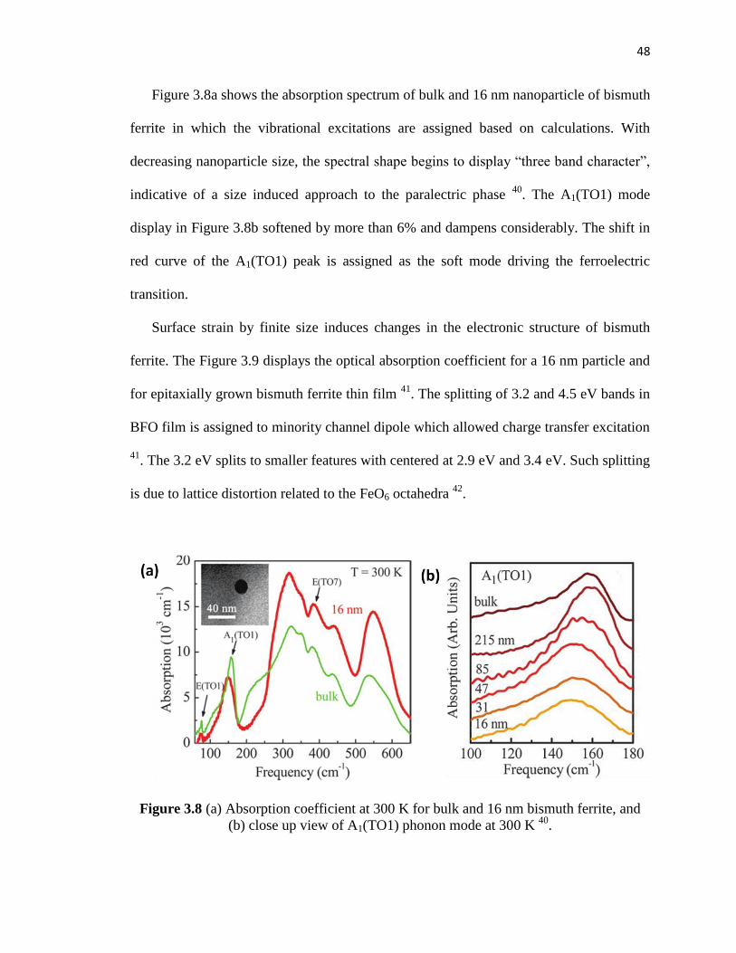
48
Figure 3.8a shows the absorption spectrum of bulk and 16 nm nanoparticle of bismuth
ferrite in which the vibrational excitations are assigned based on calculations. With
decreasing nanoparticle size, the spectral shape begins to display “three band character”,
indicative of a size induced approach to the paralectric phase 40
. The A1(TO1) mode
display in Figure 3.8b softened by more than 6% and dampens considerably. The shift in
red curve of the A1(TO1) peak is assigned as the soft mode driving the ferroelectric
transition.
Surface strain by finite size induces changes in the electronic structure of bismuth
ferrite. The Figure 3.9 displays the optical absorption coefficient for a 16 nm particle and
for epitaxially grown bismuth ferrite thin film 41
. The splitting of 3.2 and 4.5 eV bands in
BFO film is assigned to minority channel dipole which allowed charge transfer excitation
41. The 3.2 eV splits to smaller features with centered at 2.9 eV and 3.4 eV. Such splitting
is due to lattice distortion related to the FeO6 octahedra 42
.
Figure 3.8 (a) Absorption coefficient at 300 K for bulk and 16 nm bismuth ferrite, and
(b) close up view of A1(TO1) phonon mode at 300 K 40
.
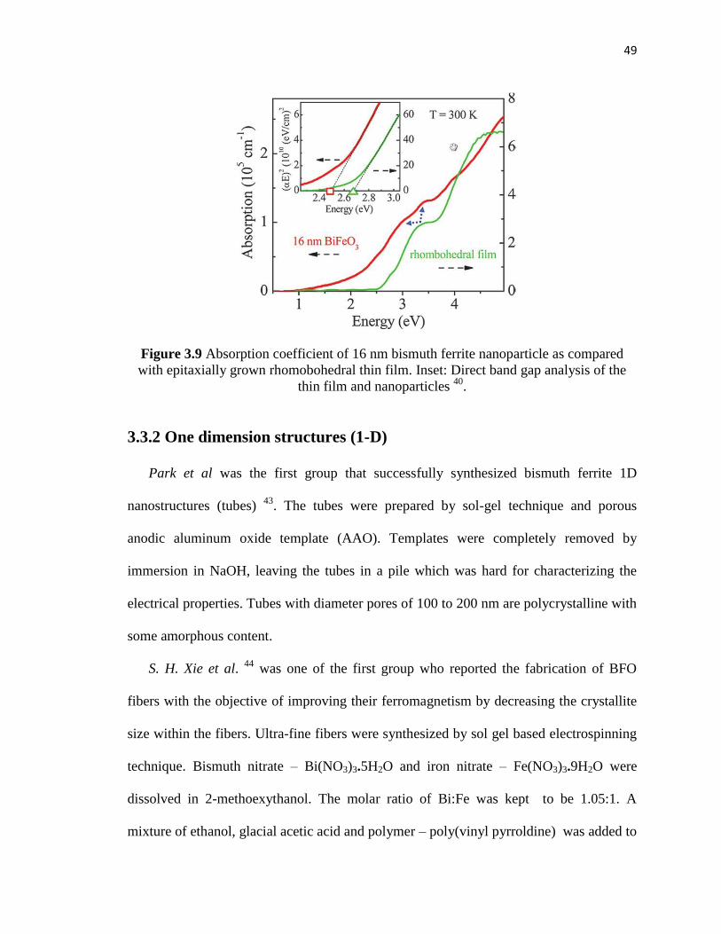
49
Figure 3.9 Absorption coefficient of 16 nm bismuth ferrite nanoparticle as compared
with epitaxially grown rhomobohedral thin film. Inset: Direct band gap analysis of the
thin film and nanoparticles 40
.
3.3.2 One dimension structures (1-D)
Park et al was the first group that successfully synthesized bismuth ferrite 1D
nanostructures (tubes) 43
. The tubes were prepared by sol-gel technique and porous
anodic aluminum oxide template (AAO). Templates were completely removed by
immersion in NaOH, leaving the tubes in a pile which was hard for characterizing the
electrical properties. Tubes with diameter pores of 100 to 200 nm are polycrystalline with
some amorphous content.
S. H. Xie et al. 44
was one of the first group who reported the fabrication of BFO
fibers with the objective of improving their ferromagnetism by decreasing the crystallite
size within the fibers. Ultra-fine fibers were synthesized by sol gel based electrospinning
technique. Bismuth nitrate – Bi(NO3)3.5H2O and iron nitrate – Fe(NO3)3.9H2O were
dissolved in 2-methoexythanol. The molar ratio of Bi:Fe was kept to be 1.05:1. A
mixture of ethanol, glacial acetic acid and polymer – poly(vinyl pyrroldine) was added to

50
the nitrates solution and stirred continuously. The solution was then loaded into a syringe
equipped with a needle. The needle was connected a high voltage supply and ground
connected to a metal collector in the opposite site. The voltage was increased up to 1.4
kV/cm and fibers were collected in glass flake (collector). The as spun fibers were heat
treated in air, nitrogen, and argon (120 ◦C for 4 hours, 350
◦C and 550
◦C for 2 hours).
Scanning electron microscopy in Figure 3.10a shows uniform ultra-fine fibers round in
shape and straight over few micrometers in length. Fired fibers have diameters in a range
of 100 to 300 nm. Crystalline fibers are obtained and impurities are reduced for fibers
fired under Ar atmosphere. High voltage PFM demonstrated the ferroelectric and
piezoelectric behavior of BFO nanofibers. The linear piezoelectric coefficient was
estimated to be around 22 pC/N, which is smaller than those reported for BFO epitaxial
thin films. Weak ferromagnetism with saturation magnetization of 4 emu/g and coercive
field of 200 Oe was measured (Figure3.10b). The enhanced magnetization may be
attributed to an intrinsic effect due the presence of impurities such as γ-Fe2O3.
Figure 3.10 (a) Scanning electron microscope image of crystallize bismuth ferrite
nanofibers, and (b) magnetic hysteresis loop 44
.

51
Dopant ion substitution engineering as another possibility that can significantly
enhance the magnetic, electric, and magnetoelectric properties of BFO is also
investigated in 1D structures. In view of variety of possibilities, Das et al 45
reported the
diameter dependent on the optical, magnetic, and magnetodielectric properties of Pr-Cr
co-doped bismuth ferrite nanowires prepared via wet chemical template assisted route.
Single phase rhomobhedral structure Pr-Cr BFO nanowires of 18, 35, 55, 100, 150, and
250 nm were prepared. Co-doping causes a bond length change in the atoms of BFO
crystal structure confirmed by a shift in the Raman peaks. The peak related with the Bi-
O1 vibrational mode around 130 cm-1
in the 200 nm, responsible for the magnetoelectric
coupling in the sample was found to shift towards a lower frequency as the nanowires
diameter increases. The gradual decrease in the peak intensity is probably due to the
grater lattice distortion or enhanced coupling between ferroelectric and magnetic order.
The magnetic response was enhanced by decreasing the nanowire diameter and
maximum saturation magnetization of 0.57 emu/g was obtained.
Figure 3.11 (a) Diameter dependence of the room temperature raman spectra of the co-
doped bismuth ferrite nanowires, and (b) diameter dependent variation of the magnetic
hysteresis loops of the co-doped nanowires measured at 300K 45
.

52
Replacing/Codoping Bi3+
with Pr ion and Fe3+
with Cr ion changes the canting angle and
increases the degree of the distortion which results in a smaller bond angle of the
antiferromagnetic Fe-O-Fe chain of spins leading to enhanced magnetization 45
.
3.3.3 Two dimension structures (2-D)
In previous section the effect of ion substitution was discussed for 1D structure. Ion
substitution in the A and/or B site of the perovskite BiFeO3 is a widely explore
alternative route to obtain low leakage current with high ferroelectric properties in 2D
structures (thin films) as well. A-site substation refers to the case were Bi3+
ions are
replaced by other elements. A-site substitution by ions with smaller ionic radius can
cause more buckling in the Fe-O-Fe angle which results in a smaller tolerance factor 46
. A
small tolerance factor favors a more insulator character in BFO. Replacing Bi3+
by
divalent ions might produce hole-doped BFO while substitution with higher valence like
4+ might produce electron carriers 46
unless other defects as oxygen vacancies are
produced. On the other hand, B-site substitution refers to the case in which Fe3+
ions are
replaced by other transition metals. The d-orbital state of the Fe3+
ion plays an important
role on the physical properties of BFO by changing its electronic structure. The
composition tuning through A or B site substitution in perovskite ferroelectric is known
to achieve a region called morphotropic base boundary (MPB) in which properties are
enhanced (maximized). An MPB region is also expected when A or B-site substitution in
BiFeO3 occurred.
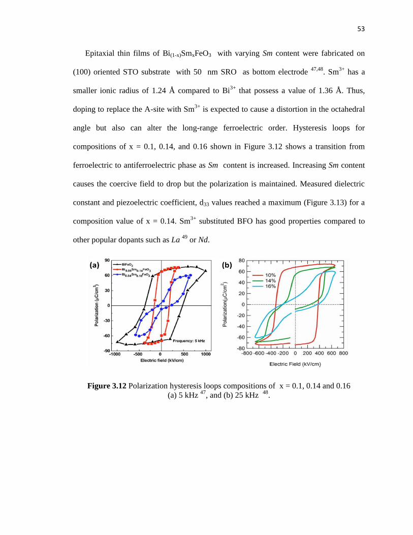
53
Epitaxial thin films of Bi(1-x)SmxFeO3 with varying Sm content were fabricated on
(100) oriented STO substrate with 50 nm SRO as bottom electrode 47,48
. Sm3+
has a
smaller ionic radius of 1.24 Å compared to Bi3+
that possess a value of 1.36 Å. Thus,
doping to replace the A-site with Sm3+
is expected to cause a distortion in the octahedral
angle but also can alter the long-range ferroelectric order. Hysteresis loops for
compositions of x = 0.1, 0.14, and 0.16 shown in Figure 3.12 shows a transition from
ferroelectric to antiferroelectric phase as Sm content is increased. Increasing Sm content
causes the coercive field to drop but the polarization is maintained. Measured dielectric
constant and piezoelectric coefficient, d33 values reached a maximum (Figure 3.13) for a
composition value of x = 0.14. Sm3+
substituted BFO has good properties compared to
other popular dopants such as La 49
or Nd.
Figure 3.12 Polarization hysteresis loops compositions of x = 0.1, 0.14 and 0.16
(a) 5 kHz 47
, and (b) 25 kHz 48
.

54
Figure 3.13 (a) Dielectric constant 33 and tan measured at 1 MHz (zero bias), and (b)
High field d33 determined from piezoelectric hysteresis loop measured as a function of
composition (not shown here) 47
.
At this point, it is clear that ion doping improves the ferroelectric properties and
reduces the leakage current. Considering that PZT is the most studied ferroelectric
material with low leakage current, useful for practical applications it could be integrated
in a binary system with BFO based compositions. Solid solution of PZT and La doped
BFO composite thin films deposited on Pt/TiO2/SiO2/Si greatly decrease the leakage
current and improve the electrical properties as shown in Figure 3.14a. Composite thin
films of 0.60Bi0.90La0.10FeO3-0.40Pb(Zr0.52Ti0.48)O3 (BLFO-PZT) were deposited without
a buffer layer through RF sputtering 35
. There is an enhancement in the dielectric constant
with a value of ~527 and a dielectric loss of ~1.9 % at 1 kHz (Figure 3.14b) which is
much larger than those of pure BFO and BLFO.

55
Figure 3.14 (a) Hysteresis loop of BLFO-PZT thin films measured at 5 kHz, and (b)
Dielectric properties measured at 1 kHz 35
Matsuo et al, investigated the ferroelectric properties of xBKT–(1-x)BFO solid solution
in the form of ceramics. The results obtained from TEM, X-ray and neutron powder
diffraction indicate that morphotropic phase boundary (MPB) region exists between 0.4 <
x < 0.43. Ceramics with MPB composition exhibited superior properties with remnant
polarization of 52 µC.cm-2
and k33 of 0.36 at room temperature 36
. Such results stimulate
the study of BKT-BFO solid solution in the form of thin films.
Multilayer thin films of BFO and one or more ferroelectric layers have been showed
to exhibit enhanced properties 29,37
. However, the coupling and interaction among the
layers can strongly influence the growth and physical properties of the thin films. Well
studied lead free ferroelectric materials such as (Bi0.5K0.5)TiO3 (BKT), BaTiO3 (BT), and
(Bi0.5Na0.5)TiO3 (BNT) are some of the potential candidates to combine in a multilayer
design with BFO, although other ferromagnetic materials are also considered. The
ferroelectric and dielectric properties of BNT and BKT ceramics are known to be
moderated in comparison with PZT compositions. BKT and BNT ceramics possess a
relatively high dielectric constant of 770 and 580 and longitudinal piezoelectric d33

56
coefficient, of 80 and 70 pC/N, respectively 50
. BNT-BKT-BT thin films has shown
remnant polarization values of ~30 C.cm-2
51,52
.
BFO/BNT bi-layered thin films deposited by radio frequency (RF) sputtering on
Pt/TiO2/SiO2/Si substrate without any buffer layer exhibit a strong (111) orientation and
enhanced properties 29
. A 60 nm BNT layer was first deposited at 650 ◦C and then 200
nm thick BFO layer was subsequently deposited on the BNT/Pt/TiO2/SiO2/Si at the same
temperature. Bi-layered was deposited at a RF power of 120 W, a based pressure of 10-6
Torr and deposition pressure of 10 mTorr with Ar and O2 at the ratio of 7:1. XRD studies
showed a pure perovskite structure with no impurity phases. However, BFO directly
deposited on Pt/TiO2/SiO2/Si exhibited a mixture of pyrochlore and perovskite phase.
BFO single layer showed poor ferroelectric properties (Figure 3.15b) while BFO/BNT bi-
layered exhibited properties comparable with similar thin film samples as shown in
Figure 3.15c. Improvement in the remnant polarization values is attributed to the
crystallinity and to the development of space charge in the interface between the layers.

57
Figure 3.15 (a) Hysteresis loops for (a) single layer BNT thin film, (b) single layer BFO
thin film, and (c) bi-layered BFO/BNT thin film 29
.
BNT-BT is another well-established ferroelectric composition that shows excellent
ferroelectric properties. It has been used as a buffer layer with the goal of reducing
leakage current 53
in bi-layered system of BiFeO3/[(Bi0.5Na0.5)0.94Ba0.06]TiO3. Thin films
were grown by a combined route of sol-gel and RF sputtering. The BNT-BT layer was
grown by sol-gel and BFO by RF sputtering with thickness of 150 nm and 280 nm
respectively. Single BNT-BT layer exhibits a polycrystalline phase, while secondary
phase of Bi25FeO40 was formed in BFO single layer. The electric properties of bi-layered
BFO/BNT-BT in Figure 3.16 shows properties as: r = 178, Pr = 40 C.cm-2
, and Ec =
386 kV/cm 38
. Experimental values for dielectric constant are lower than those calculated
when assuming a series composite connectivity of BNT-BT and BFO layers. Simply
series connection cannot be considered. The temperature dependence shown in Figure
3.16b can be described by the Arhenius equation:
(3.4)
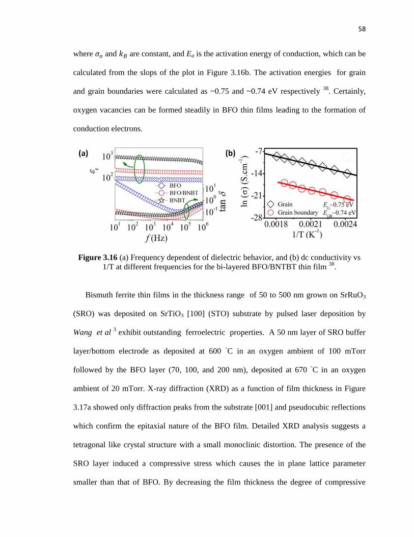
58
where and are constant, and Ea is the activation energy of conduction, which can be
calculated from the slops of the plot in Figure 3.16b. The activation energies for grain
and grain boundaries were calculated as ~0.75 and ~0.74 eV respectively 38
. Certainly,
oxygen vacancies can be formed steadily in BFO thin films leading to the formation of
conduction electrons.
Figure 3.16 (a) Frequency dependent of dielectric behavior, and (b) dc conductivity vs
1/T at different frequencies for the bi-layered BFO/BNTBT thin film 38
.
Bismuth ferrite thin films in the thickness range of 50 to 500 nm grown on SrRuO3
(SRO) was deposited on SrTiO3 [100] (STO) substrate by pulsed laser deposition by
Wang et al 3 exhibit outstanding ferroelectric properties. A 50 nm layer of SRO buffer
layer/bottom electrode as deposited at 600 ◦C in an oxygen ambient of 100 mTorr
followed by the BFO layer (70, 100, and 200 nm), deposited at 670 ◦C in an oxygen
ambient of 20 mTorr. X-ray diffraction (XRD) as a function of film thickness in Figure
3.17a showed only diffraction peaks from the substrate [001] and pseudocubic reflections
which confirm the epitaxial nature of the BFO film. Detailed XRD analysis suggests a
tetragonal like crystal structure with a small monoclinic distortion. The presence of the
SRO layer induced a compressive stress which causes the in plane lattice parameter
smaller than that of BFO. By decreasing the film thickness the degree of compressive
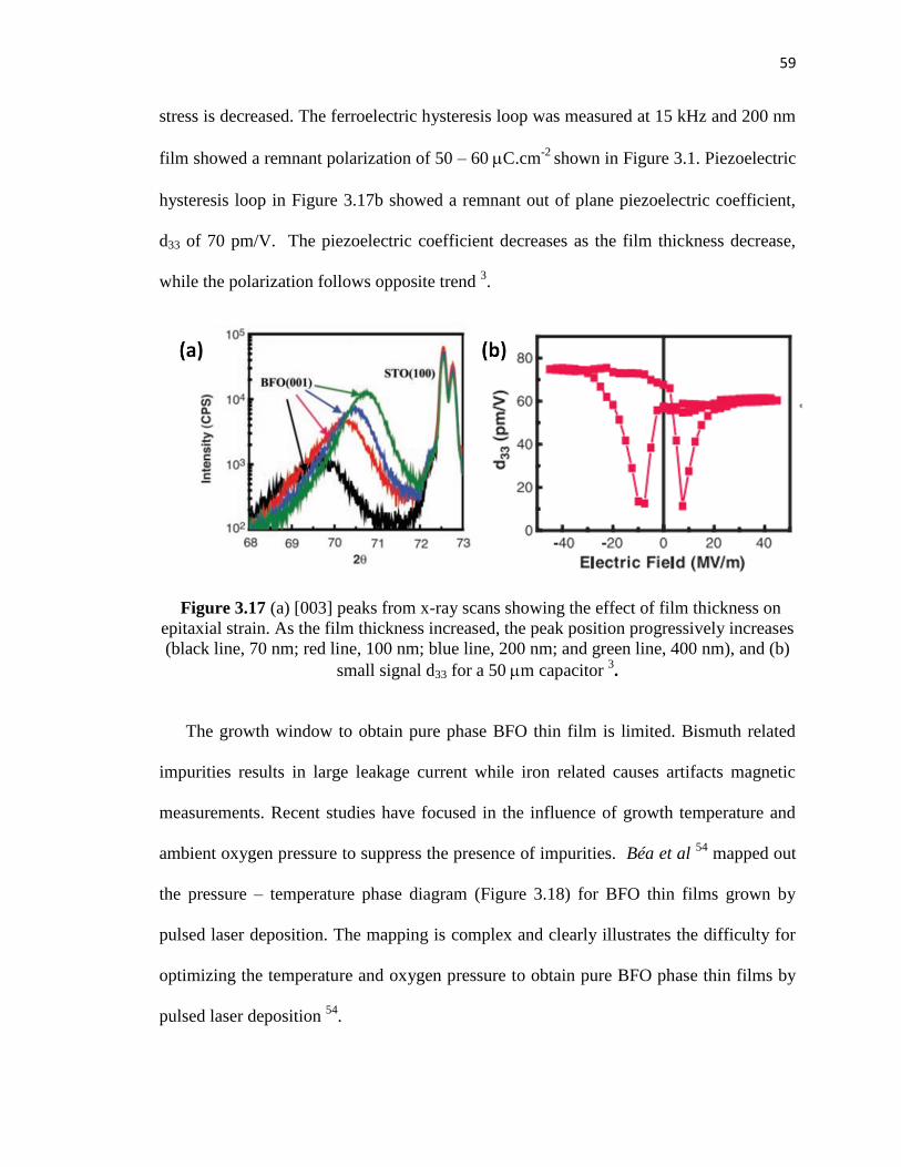
59
stress is decreased. The ferroelectric hysteresis loop was measured at 15 kHz and 200 nm
film showed a remnant polarization of 50 – 60 C.cm-2
shown in Figure 3.1. Piezoelectric
hysteresis loop in Figure 3.17b showed a remnant out of plane piezoelectric coefficient,
d33 of 70 pm/V. The piezoelectric coefficient decreases as the film thickness decrease,
while the polarization follows opposite trend 3.
Figure 3.17 (a) [003] peaks from x-ray scans showing the effect of film thickness on
epitaxial strain. As the film thickness increased, the peak position progressively increases
(black line, 70 nm; red line, 100 nm; blue line, 200 nm; and green line, 400 nm), and (b)
small signal d33 for a 50 m capacitor 3.
The growth window to obtain pure phase BFO thin film is limited. Bismuth related
impurities results in large leakage current while iron related causes artifacts magnetic
measurements. Recent studies have focused in the influence of growth temperature and
ambient oxygen pressure to suppress the presence of impurities. Béa et al 54
mapped out
the pressure – temperature phase diagram (Figure 3.18) for BFO thin films grown by
pulsed laser deposition. The mapping is complex and clearly illustrates the difficulty for
optimizing the temperature and oxygen pressure to obtain pure BFO phase thin films by
pulsed laser deposition 54
.

60
Figure 3.18 Pressure-temperature phase diagram for BFO thin films with a thickness of
70 nm 54
.
Figure 3.19 Scanning electron microscope image (a) surface of the films with low
roughness regions and of ~100 nm high square outgrowths, (b) red-green-blue image
constructed by superimposing colored element-selective mapping (red: Bi; green: Fe;
blue: O). NOTE: white scale bar corresponds to 1 m 54
.
Colored mapping in Figure 3.19 indicates that outgrowth blocks are Fe deficient and
corresponds to a BiOx phase. The areas between the blocks are homogenous in
composition. The electrical properties of BFO thin films grown by PLD were later
investigated by You et al 55
and are presented in Figure 3.20.
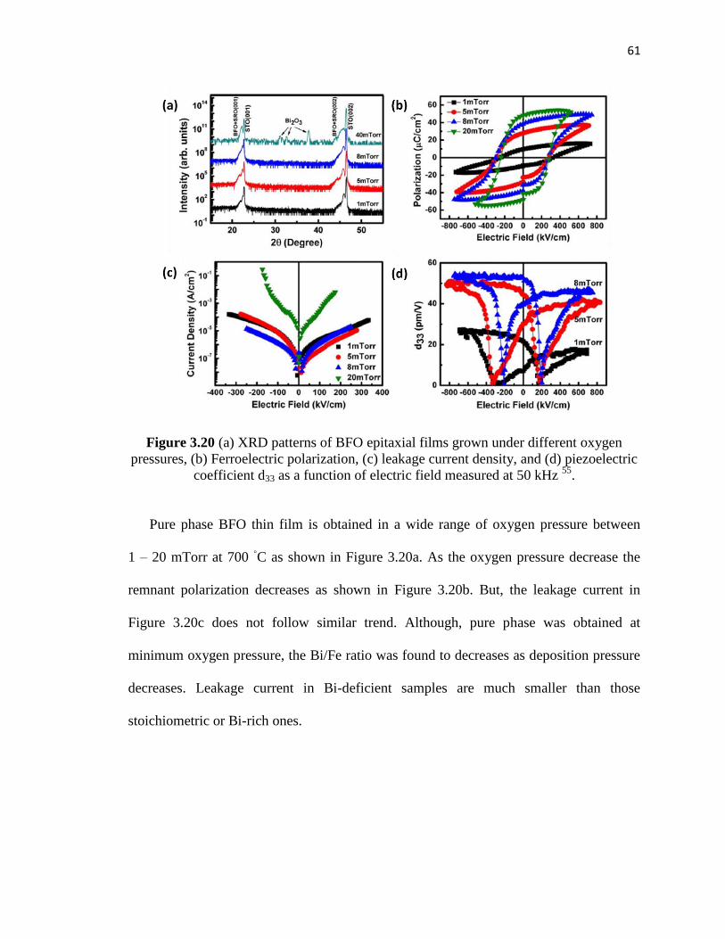
61
Figure 3.20 (a) XRD patterns of BFO epitaxial films grown under different oxygen
pressures, (b) Ferroelectric polarization, (c) leakage current density, and (d) piezoelectric
coefficient d33 as a function of electric field measured at 50 kHz 55
.
Pure phase BFO thin film is obtained in a wide range of oxygen pressure between
1 – 20 mTorr at 700 ◦C as shown in Figure 3.20a. As the oxygen pressure decrease the
remnant polarization decreases as shown in Figure 3.20b. But, the leakage current in
Figure 3.20c does not follow similar trend. Although, pure phase was obtained at
minimum oxygen pressure, the Bi/Fe ratio was found to decreases as deposition pressure
decreases. Leakage current in Bi-deficient samples are much smaller than those
stoichiometric or Bi-rich ones.

62
3.4 Summary
This chapter aimed to provide a general overview of the most important
characteristics and outstanding electronic properties of bismuth ferrite. It is difficult to
review a topic that is so popular and is continuing to develop rapidly. So, rather some of
the work that has been done and is pertinent to this investigation was considered.
There has been a progress during BFO history which resulted in a better
understanding of the structure and ferroelectric origin. Advances characterization tools
such as PFM enables the study of domains walls which revealed a unique conduction
phenomenon in BFO due to electrostatic field build up within the walls. This conduction
mechanism provides a possibility to integrate BFO in a variety of electronic devices, and
not only for storage, memory, and spintronis applications.
Although, reduced leakage current and good electromechanical properties are
obtained, often this is not the case for different processing routes. Outstanding results are
difficult to reproduce, thus causing more effort to be done in this regard. Some of these
efforts were briefly discussed in this chapter such as: ion doping, formation of multilayer
design, thin film composite, and controlled growth atmosphere for 0-D, 1-D and 2-D
bismuth ferrite nanostructures.
63
3. 5 References
1. Selbach, S. M., Einarsrud, M.-A. & Grande, T. On the Thermodynamic Stability
of BiFeO3. Chem. Mater. 21, 169–173 (2009).
2. Ting Liu, Y. X. Low‐Temperature Synthesis of BiFeO3 via PVA Sol–Gel Route.
J. Am. Ceram. Soc. 93, 3637 – 3641 (2010).
3. Wang, J. et al. Epitaxial BiFeO3 Multiferroic Thin Film Heterostructures. Science
299, 1719–1722 (2003).
4. Park, T.-J., Papaefthymiou, G. C., Viescas, A. J., Moodenbaugh, A. R. & Wong,
S. S. Size-Dependent Magnetic Properties of Single-Crystalline Multiferroic BiFeO3
Nanoparticles. Nano Lett. 7, 766–772 (2007).
5. Jaiswal, A. et al. Effect of Reduced Particle Size on the Magnetic Properties of
Chemically Synthesized BiFeO3 Nanocrystals. J. Phys. Chem. C 114, 2108–2115 (2010).
6. Joshi, U. A., Jang, J. S., Borse, P. H. & Lee, J. S. Microwave synthesis of single-
crystalline perovskite BiFeO3 nanocubes for photoelectrode and photocatalytic
applications. Appl. Phys. Lett. 92, 242106 (2008).
7. Baji, A. et al. One-dimensional multiferroic bismuth ferrite fibers obtained by
electrospinning techniques. Nanotechnology 22, 235702 (2011).
8. Zhang, X., Bourgeois, L., Yao, J., Wang, H. & Webley, P. A. Tuning the
Morphology of Bismuth Ferrite Nano- and Microcrystals: From Sheets to Fibers. Small 3,
1523–1528 (2007).
9. Dutta, D. P. et al. Effect of doping on the morphology and multiferroic properties
of BiFeO3 nanorods. Nanoscale 2, 1149 (2010).
10. Fruth, V. et al. Preparation of BiFeO3 films by wet chemical method and their
characterization. J. Eur. Ceram. Soc. 27, 937–940 (2007).
11. J. F. Ihlefeld, N. J. P. Optical band gap of BiFeO3 grown by molecular-beam
epitaxy. Appl. Phys. Lett. - APPL PHYS LETT 92, 2908–142908 (2008).
12. GA Smolenskii, Isupov, V. & Agrnovskaya, A. Ferroelectrics of the oxygen
octahedral t yoe with layered structure. Sov. Phys. Solid State 1, 650–655 (1959).
13. Achenbach, G. D., James, W. J. & Gerson, R. Preparation of Single-Phase
Polycrystalline BiFeO3. J. Am. Ceram. Soc. 50, 437–437 (1967).
14. Teague, J. R., Gerson, R. & James, W. J. Dielectric hysteresis in single crystal
BiFeO3. Solid State Commun. 8, 1073–1074 (1970).
15. Kubel, F. & Schmid, H. Structure of a ferroelectric and ferroelastic monodomain
crystal of the perovskite BiFeO3. Acta Crystallogr. Sect. B 46, 698–702 (1990).
16. Paudel, T. R., Jaswal, S. S. & Tsymbal, E. Y. Intrinsic defects in multiferroic
BiFeO3 and their effect on magnetism. Phys. Rev. B 85, 104409 (2012).
17. Jang, H. W. et al. Strain-Induced Polarization Rotation in Epitaxial (001) BiFeO3
Thin Films. Phys. Rev. Lett. 101, 107602 (2008).
18. Lubk, A., Gemming, S. & Spaldin, N. A. First-principles study of ferroelectric
domain walls in multiferroic bismuth ferrite. Phys. Rev. B 80, 104110 (2009).
19. Lebeugle, D. et al. Electric-Field-Induced Spin Flop in BiFeO3 Single Crystals at
Room Temperature. Phys. Rev. Lett. 100, 227602 (2008).
20. Streiffer, S. K. et al. Domain patterns in epitaxial rhombohedral ferroelectric
films. I. Geometry and experiments. J. Appl. Phys. 83, 2742–2753 (1998).
21. Seidel, J. et al. Conduction at domain walls in oxide multiferroics. Nat. Mater. 8,
229–234 (2009).

64
22. Catalan, G. & Scott, J. F. Physics and Applications of Bismuth Ferrite. Adv.
Mater. 21, 2463–2485 (2009).
23. Bark, C. W., Ryu, S., Koo, Y. M., Jang, H. M. & Youn, H. S. Electric-field-
induced structural modulation of epitaxial BiFeO3 multiferroic thin films as studied using
x-ray microdiffraction. Appl. Phys. Lett. 90, 022902 (2007).
24. Zhang, X. Y. et al. Synthesis and piezoresponse of highly ordered
Pb(Zr0.53Ti0.47)O3 nanowire arrays. Appl. Phys. Lett. 85, 4190–4192 (2004).
25. Urban, J. J., Yun, W. S., Gu, Q. & Park, H. Synthesis of Single-Crystalline
Perovskite Nanorods Composed of Barium Titanate and Strontium Titanate. J. Am.
Chem. Soc. 124, 1186–1187 (2002).
26. Li, B., Wang, C., Liu, W., Ye, M. & Wang, N. Multiferroic properties of La and
Mn co-doped BiFeO3 nanofibers by sol–gel and electrospinning technique. Mater. Lett.
90, 45–48 (2013).
27. Huang, Z.-M., Zhang, Y.-Z., Kotaki, M. & Ramakrishna, S. A review on polymer
nanofibers by electrospinning and their applications in nanocomposites. Compos. Sci.
Technol. 63, 2223–2253 (2003).
28. Ahadi, K., Mahdavi, S. M., Nemati, A. & Kianinia, M. Photoconductivity and
diode effect in Bi rich multiferroic BiFeO3 thin films grown by pulsed-laser deposition.
J. Mater. Sci. Mater. Electron. 22, 815–820 (2011).
29. Wu, J., Kang, G., Liu, H. & Wang, J. Ferromagnetic, ferroelectric, and fatigue
behavior of (111)-oriented BiFeO3/(Bi1/2Na1/2)TiO3 lead-free bilayered thin films.
Appl. Phys. Lett. 94, 172906 (2009).
30. Kumar, M. M., Palkar, V. R., Srinivas, K. & Suryanarayana, S. V. Ferroelectricity
in a pure BiFeO3 ceramic. Appl. Phys. Lett. 76, 2764–2766 (2000).
31. Zhu, X. H. et al. Thickness-dependent structural and electrical properties of
multiferroic Mn-doped BiFeO3 thin films grown epitaxially by pulsed laser deposition.
Appl. Phys. Lett. 93, 082902 (2008).
32. Wang, Y. A large polarization in Ce-modified bismuth ferrite thin films. J. Appl.
Phys. 109, 124105 (2011).
33. Wang, Y. & Nan, C.-W. Enhanced ferroelectricity in Ti-doped multiferroic
BiFeO3 thin films. Appl. Phys. Lett. 89, 052903 (2006).
34. Lee, Y.-H., Wu, J.-M. & Lai, C.-H. Influence of La doping in multiferroic
properties of BiFeO3 thin films. Appl. Phys. Lett. 88, 042903 (2006).
35. Wu, J., Zhang, B. & Wang, X. Bismuth ferrite composite thin films. Appl. Phys. A
111, 1017–1020 (2013).
36. Matsuo, H. et al. Structural and piezoelectric properties of high-density
(Bi0.5K0.5)TiO3–BiFeO3 ceramics. J. Appl. Phys. 108, 104103 (2010).
37. Wu, J. & Wang, J. Multiferroic behavior and impedance spectroscopy of
bilayered BiFeO3/CoFe2O4 thin films. J. Appl. Phys. 105, 124107 (2009).
38. Wu, J., Kang, G. & Wang, J. Electrical behavior and oxygen vacancies in
BiFeO3/[(Bi1/2Na1/2)0.94Ba0.06]TiO3 thin film. Appl. Phys. Lett. 95, 192901 (2009).
39. Yang, P. et al. Effect of BaTiO3 buffer layer on multiferroic properties of BiFeO3
thin films. J. Appl. Phys. 105, 061618 (2009).
40. Chen, P. et al. Size-Dependent Infrared Phonon Modes and Ferroelectric Phase
Transition in BiFeO3 Nanoparticles. Nano Lett. 10, 4526–4532 (2010).
65
41. Basu, S. R. et al. Photoconductivity in BiFeO3 thin films. Appl. Phys. Lett. 92,
091905 (2008).
42. Neaton, J. B., Ederer, C., Waghmare, U. V., Spaldin, N. A. & Rabe, K. M. First-
principles study of spontaneous polarization in multiferroic BiFeO3. Phys. Rev. B 71,
014113 (2005).
43. Park, T.-J., Mao, Y. & Wong, S. S. Synthesis and characterization of multiferroic
BiFeO3 nanotubes. Chem. Commun. 2708–2709 (2004). doi:10.1039/B409988E
44. Xie, S. H. et al. Nanocrystalline multiferroic BiFeO3 ultrafine fibers by sol-gel
based electrospinning. Appl. Phys. Lett. 93, 222904–222904–3 (2008).
45. Das, R., Khan, G. G., Varma, S., Mukherjee, G. D. & Mandal, K. Effect of
Quantum Confinement on Optical and Magnetic Properties of Pr–Cr-Codoped Bismuth
Ferrite Nanowires. J. Phys. Chem. C 117, 20209–20216 (2013).
46. Yang, C.-H., Kan, D., Takeuchi, I., Nagarajan, V. & Seidel, J. Doping BiFeO3:
approaches and enhanced functionality. Phys. Chem. Chem. Phys. 14, 15953–15962
(2012).
47. Fujino, S. et al. Combinatorial discovery of a lead-free morphotropic phase
boundary in a thin-film piezoelectric perovskite. Appl. Phys. Lett. 92, 202904 (2008).
48. Cheng, C.-J. et al. Structural transitions and complex domain structures across a
ferroelectric-to-antiferroelectric phase boundary in epitaxial Sm-doped BiFeO3 thin
films. Phys. Rev. B 80, 014109 (2009).
49. Seidel, J. et al. Domain Wall Conductivity in La-Doped BiFeO3. Phys. Rev. Lett.
105, 197603 (2010).
50. Hiruma, Y., Nagata, H. & Takenaka, T. Thermal depoling process and
piezoelectric properties of bismuth sodium titanate ceramics. J. Appl. Phys. 105, 084112
(2009).
51. Abazari, M., Safari, A., Bharadwaja, S. S. N. & Trolier-McKinstry, S. Dielectric
and piezoelectric properties of lead-free (Bi,Na)TiO3-based thin films. Appl. Phys. Lett.
96, 082903 (2010).
52. Hejazi, M., Jadidian, B. & Safari, A. Lead-free (Bi0.5Na0.5)TiO3-based thin
films by the pulsed laser deposition process. IEEE Trans. Ultrason. Ferroelectr. Freq.
Control 59, 1855–1863 (2012).
53. Wu, J., Kang, G. & Wang, J. Electrical behavior and oxygen vacancies in
BiFeO3/[(Bi1/2Na1/2)0.94Ba0.06]TiO3 thin film. Appl. Phys. Lett. 95, 192901 (2009).
54. Béa, H. et al. Influence of parasitic phases on the properties of BiFeO3 epitaxial
thin films. Appl. Phys. Lett. 87, 072508 (2005).
55. You, L., Chua, N. T., Yao, K., Chen, L. & Wang, J. Influence of oxygen pressure
on the ferroelectric properties of epitaxial BiFeO3 thin films by pulsed laser deposition.
Phys. Rev. B 80, 024105 (2009).
66
4 Characterization and Equipment Tools
4.1 Introduction
To understand the material’s electronic properties, certain information is required
such as: crystal structure, surface topography, chemical composition, chemical structure,
atomic structure, and electronic state. There is no one technique that is able to provide all
the necessary information; it will always require several techniques. In order to fully
comprehend the behavior, properties, and to solve the particular problems is necessary to
examine and analyze the different aspects of materials. This chapter is a summary of the
characterization tools used to identify and understand the phase, morphology, and
observed electronic behavior in bismuth ferrite thin films and nanofibers. The
characterization methods can be grouped as:
Physical topography: Scanning electron microscope (SEM)
Chemical composition: Rutherford backscattering spectrometry (RBS)
Chemical structure: Electron energy loss spectroscopy (EELS)
Crystal Structure: X-ray diffraction (XRD)
Electronic properties: Current vs Voltage, Current vs Time, Permittivity vs
Frequency, and Dielectric Loss vs Frequency
Most of the surface characterization methods involve bombarding the surface with a
form of radiation: electron, ions, neutrons, and collecting the resulted emitted radiation.
Surface analysis techniques: XPS, SEM, EELS, TEM, and RBS are carried out in
vacuum. The reason is because the probe/detection system such as electrons and ions are
67
scatter by molecules in the gas phase. Photons as another detection option, can in
principle, be used in ambient, but is also possible that gas absorption occurs. The
information that can be obtain from this techniques could be very revealing, however the
complexity of the materials could make difficult the interpretation and understanding of
the data using simple analysis.
In every characterization tool, it is important to understand the capabilities and
limitations of the technique being used in regard with the material, processing methods,
and require information.
4.2 X-ray diffraction
A regular array of atoms in a crystal lattice interacts elastically with short radiation,
and as a consequence a diffraction spectrum in which the incident radiation is scattered is
obtained (Figure 4.1). The diffraction angles and the intensities in the diffractions beams
are sensitive to the crystal structure of the specimen. The diffraction angles depend on the
Bravais point lattice and the unit cell dimensions of the crystal. To determine the angular
distribution of the peak intensities in the diffraction spectrum from a regular crystal
lattice is defined by the Bragg’s equation:
(4.1)
where n is an integer, λ is the wavelength of the radiation, d is the spacing of the crystal
lattice planes responsible for a particular diffracted beam, and Ɵ is the angle that the
incident beams makes with the lattice planes assuming that the angle of incidence is
equal to the angle of reflection.
68
Figure 4.1 Schematic description of Bragg’s equation 1.
X-ray diffraction (XRD) has the capability of measuring the average spacing between
the layers and rows of atoms, determining the orientation of a single crystal or
polycrystalline sample, measuring the grain size, and internal stresses of small crystalline
regions.
An X-ray diffractometer includes five major components: X-rays, the X-ray
generator, a diffractometer assembly, X-ray data collection, and analysis system as shown
in Figure 4.2. The alignment of the beam, the position and orientation of both the
specimen and X-ray detector is controlled by the diffractomer assembly. The X-rays are
generated by accelerated beam of electrons on to a pure metal (usually Mo or Cu) target
contained in a vacuum tube. These high energy electrons are ejected from the ground
state of the metal, creating holes and X-rays are emitted during the re-filling to the
ground states.

69
The resulted diffraction pattern spectrum can be analyzed in two different manners.
1) The crystalline material may be identified by comparing the diffraction angles
corresponding to the peaks with a diffraction standard. 2) The crystalline material may be
compared with a calculated spectrum derived from hypothetical model. In a general case,
a measured spectrum is compared with existing data.
Figure 4.2 Schematic of an X-ray diffraction setup.
Image source: http://ruppweb.dyndns.org/
Figure 4.3 X-ray diffraction angles for a thin film deposited on a substrate.

70
The conventional 2Ɵ X-ray diffraction geometry is not useful for the study and
analysis of thin films partially because of the poor sensitivity and the presence of the
interfering substrate. A phi scan ( ) allows to obtain crystallographic information about
thin film as well of specific orientation. In a polycrystalline sample all the grains are
randomly oriented, thus all the inclination and rotation angles (Figure 4.3) for a certain
plane will result in constant intensity. Differently, for an oriented film in a specific plane,
a diffraction peak will be observed for specific rotation and inclination angles depending
on the material’s structure. In order to examine and oriented film a phi scan/rocking
curve experiment is performed. In a rocking curve spectrum the detector is set at specific
Bragg angle and the sample is tilted. The crystal/sample will produce a sharp peak, only
when is properly tilted so that the crystallographic direction is parallel to the diffraction
vector.
4.3 Rutherford backscattering 2
Rutherford Backscattering Spectrometry (RBS) is commonly used to estimate the
chemical composition of thin films. RBS provide information such as elemental analysis,
thickness, and depth distribution. One of the major advantages of RBS technique is that
standard sample is not required to determine the composition of the sample
quantitatively. The thickness of the sample is determined by comparing a RBS spectrum
with a profile simulated by the SIMNRA software.
The principal of RBS involves mono-energetic He ions between 2 – 4 MeV. These
ions impinge perpendicularly on the sample and small portion of the ions will undergo
head on collisions with the nucleus of the sample atom on the surface as well as in depth
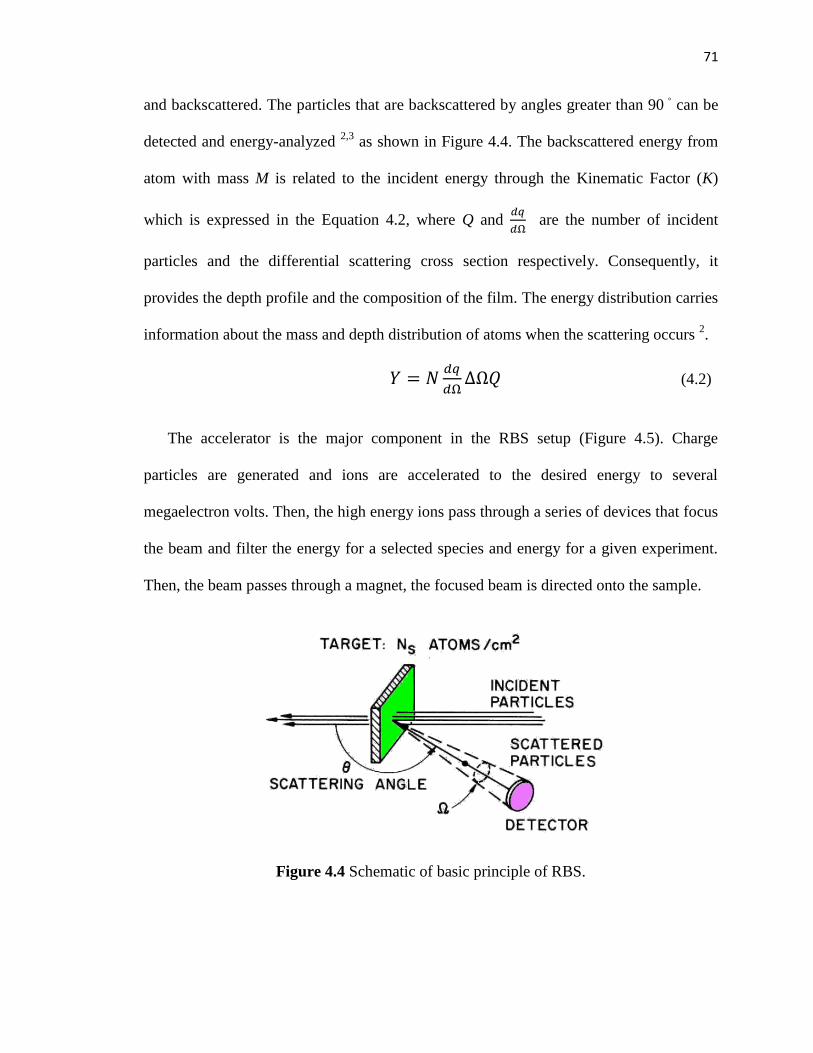
71
and backscattered. The particles that are backscattered by angles greater than 90 ◦ can be
detected and energy-analyzed 2,3
as shown in Figure 4.4. The backscattered energy from
atom with mass M is related to the incident energy through the Kinematic Factor (K)
which is expressed in the Equation 4.2, where Q and
are the number of incident
particles and the differential scattering cross section respectively. Consequently, it
provides the depth profile and the composition of the film. The energy distribution carries
information about the mass and depth distribution of atoms when the scattering occurs 2.
(4.2)
The accelerator is the major component in the RBS setup (Figure 4.5). Charge
particles are generated and ions are accelerated to the desired energy to several
megaelectron volts. Then, the high energy ions pass through a series of devices that focus
the beam and filter the energy for a selected species and energy for a given experiment.
Then, the beam passes through a magnet, the focused beam is directed onto the sample.
Figure 4.4 Schematic of basic principle of RBS.

72
Figure 4.5 Schematic diagram of a typical backscattering spectrometry setup 2.
4.4 Raman spectroscopy
Raman spectroscopy is based on inelastic scattering of a monochromatic light and
thus maybe compared with Electron Energy Loss Spectroscopy (EELS) discussed in
Section 4.8. A specimen is irradiated with a monochromatic source, usually a laser,
where photons are absorbed by the sample and then re-emitted. The frequency of the re-
emitted photons is shifted up or down in comparison with the frequency of the incident
light such effect is referred as Raman Effect. The shifted in frequency provide
information about the vibration and rotation modes that are not observed with infrared
spectroscopy (IR).
Raman Effect relies upon the polarization of the electron cloud. An incident
electromagnetic radiation with frequency, , causes a molecular deformation determined
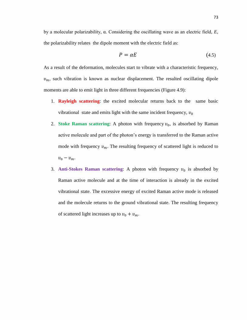
73
by a molecular polarizability, α. Considering the oscillating wave as an electric field, E,
the polarizability relates the dipole moment with the electric field as:
(4.5)
As a result of the deformation, molecules start to vibrate with a characteristic frequency,
, such vibration is known as nuclear displacement. The resulted oscillating dipole
moments are able to emit light in three different frequencies (Figure 4.9):
1. Rayleigh scattering: the excited molecular returns back to the same basic
vibrational state and emits light with the same incident frequency,
2. Stoke Raman scattering: A photon with frequency , is absorbed by Raman
active molecule and part of the photon’s energy is transferred to the Raman active
mode with frequency . The resulting frequency of scattered light is reduced to
.
3. Anti-Stokes Raman scattering: A photon with frequency is absorbed by
Raman active molecule and at the time of interaction is already in the excited
vibrational state. The excessive energy of excited Raman active mode is released
and the molecule returns to the ground vibrational state. The resulting frequency
of scattered light increases up to .
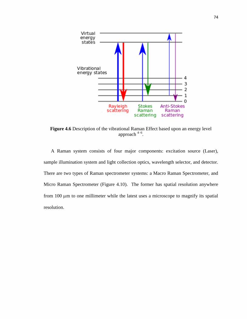
74
Figure 4.6 Description of the vibrational Raman Effect based upon an energy level
approach 4–6
.
A Raman system consists of four major components: excitation source (Laser),
sample illumination system and light collection optics, wavelength selector, and detector.
There are two types of Raman spectrometer systems: a Macro Raman Spectrometer, and
Micro Raman Spectrometer (Figure 4.10). The former has spatial resolution anywhere
from 100 m to one millimeter while the latest uses a microscope to magnify its spatial
resolution.
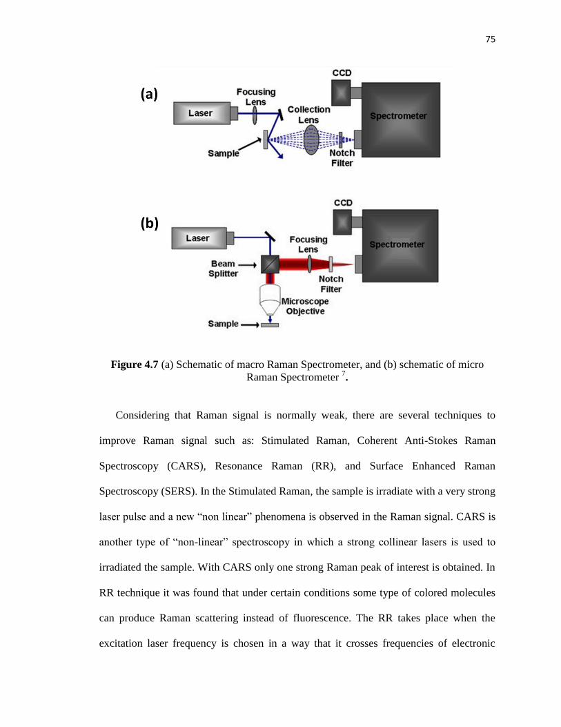
75
Figure 4.7 (a) Schematic of macro Raman Spectrometer, and (b) schematic of micro
Raman Spectrometer 7.
Considering that Raman signal is normally weak, there are several techniques to
improve Raman signal such as: Stimulated Raman, Coherent Anti-Stokes Raman
Spectroscopy (CARS), Resonance Raman (RR), and Surface Enhanced Raman
Spectroscopy (SERS). In the Stimulated Raman, the sample is irradiate with a very strong
laser pulse and a new “non linear” phenomena is observed in the Raman signal. CARS is
another type of “non-linear” spectroscopy in which a strong collinear lasers is used to
irradiated the sample. With CARS only one strong Raman peak of interest is obtained. In
RR technique it was found that under certain conditions some type of colored molecules
can produce Raman scattering instead of fluorescence. The RR takes place when the
excitation laser frequency is chosen in a way that it crosses frequencies of electronic
76
excited states and resonates with them. SERS is an enhancement of polarizability because
charges transfer effect or chemical bond formation between the metal surface and the
molecules under study.
Advantages of Raman Spectroscopy include ease of sample preparation, is a non
destructive technique, and it can be perform using with any operating range from UV to
NIR. Vibrational spectra are typically as frequency spectra as a function of intensity.
4.5 Electron microscopy: transmission electron microscopy and
scanning electron microscopy 8,9
Electron microscope uses accelerated electron as the illumination source and as a
result has a higher resolution power that reveal the features of smaller object. Different
than usual optical microscope, electron microscope is upside down. In the TEM the
source of electrons is at the top of the microscope or the “column” while the collecting
system is in the bottom. The main components in the microscope are (Figure 4.11):
electron gun maintained at high voltage (100 - 400 kV)
heated tungsten filament capable of generating electron beam current in the order
of 5 x 10⁴ A.m
-2
electromagnetic condenser lens system that focuses the high energy electron
beam
specimen stage which allows for tilting as well as some z-adjustment
objective lenses allows the fine focusing of the image
final imaging system which also uses electromagnetic lenses
fluorescence screen where the final image is observed

77
The scanning electron microscope (SEM) uses a probe lens to focus the beam instead
of electromagnetic condenser system. The electromagnetic probe lens in the SEM fulfils
a similar purpose to the objective lens in the TEM and determines the ultimate resolution
of the specimen. In the SEM, the objective lens is placed above the specimen. When the
probe interacts with the sample, inelastic scattering occurs and as a result of such
interaction the image is collected. The power of the SEM has to do with the wide range
of signals that may result as a consequence of the interaction between the electron probe
and the sample surface such as: characteristics X-rays, cathodoluminescent, backscattered
electrons, and secondary electron.
The basic difference in the operation between the TEM and SEM lied in the modes of
data collection. In the TEM information is collected continuously while in the SEM is
collected sequentially for each data point. In the SEM the scanning speed must be
restricted in order to ensure that the specimen signal is collected for each point.
Sample preparation for TEM is not simple but techniques are available for doing so
such as: mechanical thinning, electrochemical thinning, and ion milling. For SEM
imaging, the specimen must be electrically conductive to avoid the accumulation of
charge at the surface. In case of insulative sample it must be coated with a metal such as
Au or C. TEM is more powerful to study crystallographic defects down to the nanoscale
range while SEM is more powerful technique for surface characterization.

78
Figure 4.8 Schematic of the scanning electron microscope and transmission electron
microscope.
Table 4.1 Comparison between TEM and SEM
TEM SEM
Primary image is focused by the objective
lens, a set of other imaging lenses enlarge
the final image.
Image is developed point by point
generated by the interaction of focused
probe as it scanned across the surface.
Depth of field exceeds the resolution by at
least two orders of magnitude
Depth of field is typically of the order of
microns, resolution to the nanometer range
Specimen is placed close to the back focal
plane of the objective lens
Specimen is placed beneath the probe lens
it has a long working distance
Specimen diameter is typically less than 3
mm
Specimen size are similar to those used in
optical microscope about 20-30 mm

79
4.6 Electron energy loss spectroscopy 4,8,12
Electron energy loss spectroscopy (EELS) is a technique based on the primary
process of an electron excitation, which results in the fast loosing energy use to identify
the chemical composition. When a specimen is exposed to electrons with known kinetic
energy, some of them will undergo inelastic scattering in which they lose energy and
their “original” path is deflected. The transmitted beam (Figure 4.15) is collected in a
high resolution electron spectrometer in which the electrons are separated according to
their kinetic energy and as result the amount of energy that was loss is measured.
Figure 4.9 Signals and types of scattering 13
.
A spectrum of the number of electrons (scattered intensity) as a function of their
decreased kinetic energy is obtained. A typical loss spectrum is shown in Figure 4.16
over a range of 1000 eV. Four processes 8 may contribute to the energy looses of the
electron beam among which two of them can be detected with magnetic spectrometers.

80
1. Phonon excitations: results in small energy losses less than kT, these peaks
are within the zero-loss spectrum
2. Electron transitions: within and between different shells of the atoms;
energy range of 1 – 50 eV; peaks can be detected in the spectrum; used to
identify the phase in which a specific element is present
3. Plasmon excitation: associated with oscillations in the conduction band;
energy range 5 – 50 eV; interpreted in chemical terms; controversial
interpretation
4. Absorption edges associated with atomic ionization: energy range above 50
eV; accessible for chemical analysis
Figure 4.10 An EELS spectrum showing the zero loss peaks and low energy loss region
at reduced gain and an excitation absorption edge 8.
The zero loss peak is characteristic of electrons that are elastically scattered. Low loss
peak is related to interaction with electrons weakly bounded to the outer shell. For higher
loss there is an interaction with electrons in the inner shell causing excitation from the
ground state into an unoccupied shell above the Fermi level.
81
The energy resolution of the magnetic spectrometers used in EELS is better than 1
eV, and resolutions of the order of 0.5 eV are reported when using a field emission gun.
However, in most cases, it is the energy beam spread which limits the EELS resolution,
and not the features of the EELS detector. It is recommended to collect the zero loss peak
which corresponds to the first Gaussian peak for the beam exiting the specimen and used
it to calibrate both the absolute zero for the spectrum and to estimate the energy
resolution. The EELS technique is very sensitive and can detect signal from less than a
few thousands atoms. The peak intensity depends on the physics of the primary
excitation.
In this technique there is no need of a standard sample. The core – loss intensities can
be converted to the elemental ratio using cross sections. These cross sections are known
for most of the K edges and L edges. Thus, the simplest method of finding quantitative
estimates is by taking the ratios of the data derived from each edge.
4.7 Electrical characterization
In order to measure the electrical properties of bismuth ferrite thin films and
nanofibers Au electrodes were deposited as top electrode. For BFO based thin films
prepared by PLD, Au top electrodes of 200 m in diameter and 50 nm in thickness were
deposited by DC sputtering using a metallic shadow mask. For BFO based nanofibers
prepared by electrospinning, Au top electrodes of 50 nm in thickness and 50 m in width
were deposited by DC sputtering.

82
4.7.1 Current vs voltage & current vs time (Light On/Light Off)
The IV measurements were done using two-probe system and a HP-Agilent source
meter. Voltage was applied between the two gold electrodes and current passing between
them was measured. To study the photoconductive (It) response a solar simulator with
AM 1.5 spectra output was chosen as the light source. A constant voltage was applied
between the two gold electrodes and the variation in the current was measured upon
illumination of the nanofibers to the light. While the light source was switched On/Off
the current was measured. The On/Off ratio was calculated from the current values with
the Light On over the current when Light Off.
Figure 4.11 The sample is placed under the light source. (a) Light On, (b)
Light Off, and (c) Current vs Time plot upon sample illumination.
83
4.7.2 Ferroelectric and dielectric measurements
The ferroelectric, leakage current (I-V plot), and dielectric properties of thin films
were studied using a ferroelectric test system (Precision LC, Radiant Inc.) and LCR meter
(HP4284A) at room temperature. The P-E hysteresis loop was measured at a pulse width
of 10ms using a triangular wave signal. The dielectric constant and dissipation factor
were studied at zero bias fields and an oscillation level of 50mV. Thin films
microstructure was studied by a field emission scanning electron microscopy (FESEM-
Zeiss, Sigma) operated between 3 to 5 kV.
4.8 Summary
This chapter discussed fundamental principles of characterization techniques used in
this investigation to understand the behavior and properties of bismuth ferrite thin films
and nanofibers. The crystallographic structure and orientation of grown thin films films
and nanofibers are studied with phi scan x-ray diffraction and rocking curve. The
composition and chemical structure was determined by a combination of techniques
which included XPS, RBS, Raman Spectroscopy, and EELS. Finally, the surface
topography was studied by electron microscopy such as TEM and SEM.
84
4.9 References
1. Wide Angle X-ray Diffraction Studies of Liquid Crystals. OpenStax-CNX at
<http://cnx.org/content/m46154/latest/?collection=col10699>
2. Chu, W.-K., James Mayer W. & Nicolet, M. A. Backscattering Spectrometry.
(Elsevier, 2012).
3. Tu, K. & Rosenberg, R. Analytical techniques for thin films. (Academic Press,
1988).
4. Vickerman, J. C. & Gilmore, I. Surface Analysis: The Principal Techniques.
(Wiley, 2009).
5. Raman spectroscopy. Wikipedia, the free encyclopedia (2014). at
<http://en.wikipedia.org/w/index.php?title=Raman_spectroscopy&oldid=613655348>
6. Kalantri, P. P., Somani, R. R. & Dinesh T. Makhija. Raman Spectroscopy: A
potential technique in analyis of pharmaceuticals. Chem. Sin. 1, 1–12 (2010).
7. Surface-Enhanced Raman Spectroscopy for the Study of Surface Chemistry.
OpenStax-CNX at <http://cnx.org/content/m34522/latest/?collection=col10699>
8. Brandon, D. & Kaplan, W. D. Microstructural Characterization of Materials.
(John Wiley & Sons, 2008).
9. Reimer, L. Scanning Electron Microscopy: Physics of Image Formation and
Microanalysis. (Springer, 1998).
10. Atomic force microscopy. Wikipedia, the free encyclopedia (2014). at
<http://en.wikipedia.org/w/index.php?title=Atomic_force_microscopy&oldid=61164487
6>
11. Haugstad, G. Atomic Force Microscopy: Understanding Basic Modes and
Advanced Applications. (John Wiley & Sons, 2012).
12. Egerton, R. Electron Energy-Loss Spectroscopy in the Electron Microscope.
(Springer, 2011).
13. Williams, D. B. & Carter, C. B. Transmission Electron Microscopy: A Textbook
for Materials Science. (Springer, 2009).
85
5 Bismuth Ferrite Thin Film by Sol-Gel
5.1 Introduction
As discussed in Chapter 3 bismuth ferrite has attracted a great deal of attention due to
its multiferroic properties at room temperature and as a potential candidate for
photovoltaics. In spite of its good ferroelectric properties with high remnant polarization,
there are still some arguments on such characteristics. Therefore, further studies are being
conducted to elucidate the ferroelectric origin and properties. One of the serious issues in
BFO is its high leakage current at room temperature in both ceramic and thin films. As a
result, breakdown occurs even at low electric field thereby creating a problem in the
observation of saturation in the ferroelectric hysteresis loop (domain switching). A great
effort is being done to overcome leakage current issue which has been discussed
previously.
In order to understand and correlate bismuth ferrite system/properties from different
perspective, thin films have been fabricated through a variety of methods which involve:
pulsed laser deposition 1–3
, metal organic chemical vapor deposition, physical vapor
deposition, chemical solution deposition 4–6
, and molecular beam epitaxy 7. Among all
techniques, chemical solution deposition (CSD) is attractive because of it’s a versatility
to prepare oxide thin films. It is expected to provide high homogeneity, low temperature,
and control of chemical composition. Bismuth ferrite thin films have been prepared by
CSD process using different combinations of solvents such as ethylene glycol, acetic
acid, 2-methoexyethanol, and propionic acid. Each combination requires complex
solution synthesis methods to effectively adjust the viscosity, solubility and surface
86
tension in the precursor which will later affect the thin film deposition. On the other
hand, substitution of various ions in the Fe site has been examined with the purpose of
improving the insulating resistance. It is reported that Mn-doped ABO3 perovskite
ferroelectric thin films have shown enhanced leakage current and reduced dielectric loss
8–13. Substitution of Mn in the Fe site of BiFeO3 plays an important role in controlling the
valence fluctuation of Fe and reducing the carrier concentration in the film 14
. Donor
doping with Mn is expected to fill the oxygen vacancies and thus increase the electrical
resistivity of BFO.
In this chapter, an attempt has been made to prepare BFO- Mn doped thin films by
sol-gel method and evaluated its microstructure and leakage current. The thin films
crystallinity, and phase are discussed in relation with the leakage current density.
5.2 Experimental procedure
Bismuth ferrite-based (BiFe1-xMnxO3; x= 0, 0.05, 0.10, 0.15) thin films were prepared
by chemical solution deposition (CSD) spin coating method. Precursor solution was
prepared by dissolving equal amounts (0.5g) of Bi(NO3)3.5H2O, Fe(NO3)3
.9H2O, and
Mn(NO3)2.4H2O in a combination of 2-methoexyethanol (2MEO) and glacial acetic acid
(GAC) in a 2:1 ratio. The combination of 2MEO and GAC was selected as a solvent
because of its ability to dissolve a wide range of precursor and to adjust the viscosity and
surface tension. Individual solutions were kept under stirring for one hour, after
dissolution they were added according to stoichiometric composition. Final molarity was
adjusted by adding 2MOE. In order to minimize particulate contamination, the solution
was filtered. The filtered solution was spin coated at 3000 rpm for 30 seconds to deposit

87
one layer of thin film on a commercial Pt/Ti/SiO2/Si substrate. Each layer was pyrolized
at 300 ◦C for 2 minutes in a hot plate. The spin coating and pyrolysis processes were
repeated several times to increase the film thickness. Finally, the film was placed in the
furnace at 550 ◦C for 10 minutes and cooled rapidly. The described process is
summarized in Figure 5.1.
Figure 5.1 Flowchart of sol-gel deposition procedure.

88
5.3 Results and discussion
Figure 5.2 shows the XRD patterns for BiFe1-xMnxO3 (x=0.00, 0.05, 0.10, 0.15) films.
The XRD indicate that pure polycrystalline BFO films formed with no secondary phase
up to 15% Mn doping. Mn atoms has a similar ionic radii to Fe (0.675 Å), thus the
substitution tolerance of Mn in BFO is high and formation of secondary phase was not
reported even in 50 % Mn substituted in films 9 and ceramics
10. Figure 5.2c shows the
magnified patterns in the vicinity of 2-theta = 31◦. As shown in the figure, pure BFO
exhibits a minor separation between (104) and (110) reflections, which indicates the
distorted perovskite rhombohedral structure with R3c space group. When Mn is
introduced the peak reflections are shifted and overlapped to a single broad peak 9. This
results indicated that there is a change in the lattice parameter by Mn substitution and
suggest that the rhombohedral structure of un-doped BFO film is modified and reduced
towards the tetragonal structure. The (012) peak in Figure 5.2b is observed to be shifted
towards a higher angle with Mn doping which is in agreement with a possible change in
the lattice parameters as a function of Mn content.

89
Figure 5.2 X-ray diffraction patterns for BFO-Mn doped thin films.
The effect of Mn doping is further reflected in the Raman spectra of the x= 0.00 to
0.15 samples as shown in Figure 5.3. Raman spectroscopy in the microscopic scale is
able to probe local changes in the structure 15
. The rhombohedral (R3c) structure of BFO
give rises to 13 Raman actives modes listed as 4A1 + 9E 16,17
. In this study 12 and 10
Raman actives modes were identified for un-doped and 5% Mn doped thin films
respectively. It is clear from Figure 5.3 that increasing Mn > 5% content gives rise to
broad and less intense Raman bands associated with the normal modes in pure BFO.
There is no appearance of extra bands in the doped samples, thus it appears that doping

90
with Mn in BFO affects the perovskite related phonon modes which are associated with a
tilting of the FeO6. The increase in wave numbers for some of the higher Raman modes
can perhaps be attributed to an increase in the Mn-O bonding compared to Fe-bonding 15
.
The obtained peak position in this study and the comparison with reported values for
BFO single crystal and epitaxial thin film is shown in Table 5.1.
Figure 5.3 Raman Spectroscopy for BiFe1-xMnxO3 thin films as function of Mn content.
100 200 300 400 500 600 700 800
R
am
an
In
ten
sit
y (
a.u
.)
Wavenumber (cm-1)
x=0.00
x=0.05
x=0.10
x=0.15
91
Table 5.1 Comparison of the Raman mode peak positions from the present study and
the literature
Raman mode
(cm-1
)
Present Study
x = 0.00
Present Study
x = 0.05
Single Crystal
16
Epitaxial thin
film 18
A1-1 140 135 147 136
A1-2 170 170 176 168
A1-3 219 219 227 211
A1-4 498 _ 490 425
E 262 258 265 275
E 271 341 279 335
E 344 _ 351 365
E 369 389 375 _
E 474 474 437 456
E 543 607 473 549
E 599 622 525 597
E 88 90 77 _
E _ _ 36 _
The surface morphology and cross section of the pure BFO and Mn doped thin films
were studied using field emission SEM as shown in Figure 5.4. Un-doped BFO thin films
exhibited a smooth surface with minor presence of particulates. Individual grains are not
distinguished for low Mn content thin films (x = 0.00 to x = 0.10). The surface of the
films becomes rougher and a combination of small and larger grains are observed when
the amount of Mn increased to 15 % (Figure 5.4g). The cross section images showed a
92
dense and continuous thin film through the overall thickness of 200 nm for lower doping
level. Mn 15% doped films show a columnar growth.
Figure 5.4 FESEM micrographs of BiFe1-xMnxO3 thin film surface (left side) and cross
section (right side). (a-b) x = 0.00, (c-d) x = 0.05, (e-f) x = 0.10, and (g-h) x = 0.15
93
Figure 5.5 shows the electrical behavior of BFO and BFO-Mn 5% measured at 1 kHz and
room temperature. Pure BFO thin films exhibited a poor ferroelectric loop, a so called
“banana loop” in which saturation is not observed (Figure 5.5a). In comparison with un-
doped BFO films, the hysteresis loop of the Mn 5% films prepared under the same
processing conditions show higher remnant polarization. However, saturation still is not
achieved and the loop shape is not desirable. The coercive field for 5% Mn-doped thin
film is found to be about 300 kV/cm (Figure 5.5b) which is larger than reported value for
epitaxial BFO film 1. The leakage current as a function of electric field for un-doped and
5% Mn doping is shown in Figure 5.5c. The leakage current value for un-doped BFO is
small at lower voltages and sharply increases at higher voltages. The leakage current for
5% Mn doped films is suppressed by approximately two orders of magnitude and
gradually increases with applied voltage. Such a decrease is expected to improve the
ferroelectric properties.
As a result of the low electrical resistivity of BFO at room temperature, most of the
reported ferroelectric behavior are measured at higher frequencies in the range of 10 to 25
kHz 1. The temperature or frequency dependence of ferroelectric properties suggests that
domain wall motion is an important factor in determining the electrical properties of
BFO. Despite the fact that leakage current was decreased, the breakdown field of the
films, at which the conductivity starts to increase sharply, was low at room temperature.
Such value is lower than the reported coercive field of the films 1,19
, and thus is possible
to obtain a saturated polarization hysteresis loop at room temperature. High electric field
is necessary to switch the domains which can be achieved at lower temperature without
the film breakdown. H. Amorín et al described such behavior as dipolar effect in which

94
Fe2+
ions and oxygen vacancies clamps ferroelectric domains 20
. Considering the multi-
valence of Mn substitution for Fe, charge compensation can occur by the formation of A-
site (Bi) or B-site (Fe) vacancy which is associated with oxygen vacancy. These point
defects are mobile and can diffuse to more energetically favorable positions which act as
a potential well. Considering same external applied field, the diffusion velocity for
ion/cation and oxygen vacancies varies and defects could combine during this process.
On the other hand, at low temperature, the potential well intensifies and leads to trapped
point defect and the probability of combining decreases. The intensified potential well
increases trapped point defect induces and enhances domain pinning. In order to switch
the strong pinned domains, high coercive field is necessary. Consequently, at lower
temperatures there are more frozen domains and higher remnant polarization could be
obtained.
The films doped with x > 10% exhibited a high leakage current with a rounded
hysteresis loop (not shown here).

95
Figure 5.5 (a) Polarization hysteresis loop for BFO thin film, (b) Polarization hysteresis
loop for BiFe0.95Mn0.05O3 thin film, and (c) leakage current as a function of electric field
for BFO and BFO-Mn thin film Note: 20 layers is equivalent to an overall thickness of
200 nm.

96
5.4 Summary
In this chapter, un-doped and Mn doped (x = 0.01 to 0.15) bismuth ferrite thin films
of 200 nm in thickness have been fabricated and deposited on Pt/Ti/SiO2/Si substrate
through chemical solution/spin coating process. X-ray diffraction analysis revealed that
the obtained films were composed of polycrystalline grains with a perovskite structure.
Increasing Mn content resulted in structural change from rhombohedral to tetragonal for
x > 5% which is also confirmed by a peak shift in the Raman phonon actives modes.
There is no evidence of impurity up to 15% Mn doping. Cross section imaging obtained
from FESEM showed the columnar type growth of thin film. The leakage current density
of the un-doped films was successfully reduced by two orders of magnitude with 5% Mn
doping. However, saturated polarization with electric filed is not achieved. The value at
which the hysteresis loop started to become rounded (breakdown) is lower than the
coercive field of reported BFO. Therefore, a different thin film processing approach is
proposed to effectively reduce the leakage current density and coercive field which is
discussed in the next chapter.

97
5.5 References
1. Wang, J. et al. Epitaxial BiFeO3 Multiferroic Thin Film Heterostructures. Science
299, 1719–1722 (2003).
2. Jiang, K. et al. Influences of oxygen pressure on optical properties and interband
electronic transitions in multiferroic bismuth ferrite nanocrystalline films grown by
pulsed laser deposition. ACS Appl. Mater. Interfaces 3, 4844–4852 (2011).
3. Wang, C. et al. Leakage current of multiferroic (Bi0.6Tb0.3La0.1)FeO3 thin films
grown at various oxygen pressures by pulsed laser deposition and annealing effect. J.
Appl. Phys. 99, 054104 (2006).
4. Liu, H. R., Liu, Z. L., Liu, Q. & Yao, K. L. Ferroelectric properties of BiFeO3
films grown by sol-gel process. Thin Solid Films 500, 105–109 (2006).
5. Shannigrahi, S. R., Huang, A., Chandrasekhar, N., Tripathy, D. & Adeyeye, A. O.
Sc modified multiferroic BiFeO3 thin films prepared through a sol-gel process. Appl.
Phys. Lett. 90, 022901 (2007).
6. Fruth, V. et al. Preparation of BiFeO3 films by wet chemical method and their
characterization. J. Eur. Ceram. Soc. 27, 937–940 (2007).
7. J. F. Ihlefeld, N. J. P. Optical band gap of BiFeO3 grown by molecular-beam
epitaxy. Appl. Phys. Lett. - APPL PHYS LETT 92, 2908–142908 (2008).
8. Hejazi, M., Taghaddos, E., Gurdal, E., Uchino, K. & Safari, A. High Power
Performance of Manganese-Doped BNT-Based Pb-Free Piezoelectric Ceramics. J. Am.
Ceram. Soc. n/a–n/a (2014). doi:10.1111/jace.13098
9. Singh, S. K., Ishiwara, H. & Maruyama, K. Room temperature ferroelectric
properties of Mn-substituted BiFeO3 thin films deposited on Pt electrodes using chemical
solution deposition. Appl. Phys. Lett. 88, 262908 (2006).
10. Palkar, V. R., Kundaliya, D. C. & Malik, S. K. Effect of Mn substitution on
magnetoelectric properties of bismuth ferrite system. J. Appl. Phys. 93, 4337–4339
(2003).
11. Li, B., Wang, C., Liu, W., Ye, M. & Wang, N. Multiferroic properties of La and
Mn co-doped BiFeO3 nanofibers by sol–gel and electrospinning technique. Mater. Lett.
90, 45–48 (2013).
12. Singh, S. K., Ishiwara, H., Sato, K. & Maruyama, K. Microstructure and
frequency dependent electrical properties of Mn-substituted BiFeO3 thin films. J. Appl.
Phys. 102, 094109 (2007).
13. Yu, X. & An, X. Enhanced magnetic and optical properties of pure and (Mn, Sr)
doped BiFeO3 nanocrystals. Solid State Commun. 149, 711–714 (2009).
14. Yoneda, Y. & Sakamoto, W. Electronic and local structures of BiFeO3 films. J.
Phys. Condens. Matter 23, 015902 (2011).
15. Somdutta Mukherjee, R. G. Influence of Zr doping on the structure and
ferroelectric properties of BiFeO3 thin films. J. Appl. Phys. 107, 123535 – 123535–5
(2010).
16. Fukumura, H. et al. Raman scattering study of multiferroic BiFeO3 single crystal.
J. Magn. Magn. Mater. 310, e367–e369 (2007).
17. Palai, R. et al. β phase and γ-β metal-insulator transition in multiferroic BiFeO3.
Phys. Rev. B 77, (2008).

98
18. Singh, M. K., Jang, H. M., Ryu, S. & Jo, M.-H. Polarized Raman scattering of
multiferroic BiFeO3 epitaxial films with rhombohedral R3c symmetry. Appl. Phys. Lett.
88, 042907 (2006).
19. Singh, S. K. & Ishiwara, H. Reduced Leakage Current in BiFeO3 Thin Films on
Si Substrates Formed by a Chemical Solution Method. Jpn. J. Appl. Phys. 44, L734
(2005).
20. Amorín, H. et al. Multiferroism and enhancement of material properties across the
morphotropic phase boundary of BiFeO3-PbTiO3. J. Appl. Phys. 115, 104104 (2014).

99
6 Bismuth Ferrite Thin Films by Pulsed Laser Deposition
6.1 Introduction
Several deposition techniques such as sol-gel, chemical solution deposition (CSD) 1,2
,
radio frequency sputtering (RF) 3,4
, molecular beam epitaxy (MBE) 5,6
, and pulsed laser
deposition (PLD) 7–9
have been employed for the deposition of BFO based thin films.
Among them PLD is a popular technique due to the capability to deposit complex oxides,
which allow the growth of high quality thin films. In the PLD method, presence of
oxygen pressure during film growth significantly affects the crystallization, phase purity,
and eventually properties of the films. A great deal of research is accomplished in
deposited bismuth ferrite thin films with PLD techniques for multiferroic applications
This chapter is focused on the investigation of thin films with following target
composition deposited on (001) oriented SrTiO3 substrate as shown in Figure 6.1:
1. Pure BiFeO3
2. Solid solution of BiFeO3-(Bi, K)TiO3
3. BFO and BNT-BKT-BT targets to develop bi-layered thin films.
Figure 6.1 Schematic of three different thin film design deposited by PLD.
100
6.2 Experimental procedure
6.2.1 Powder and target preparation
The preparation of the PLD ceramic target for the fabrication of thin film is similar to
the fabrication of bulk ferroelectric ceramic. Mixed-oxide route was employed for
powder and ceramic processing. The process was optimized to obtain a high quality
target. The characteristics of the target regarding the density, purity and phase uniformity
is important for the film quality. The high quality PLD target plays an important role on
the preparation, structure, and properties of thin films.
Different BFO based compositions were prepared using Bi2O3 (99.9%, Aldrich),
Fe2O3 (<99%, Alfa Aesar), K2CO3 (99.99%, Alfa Aesar), TiO2 (99.5%, Aldrich), Na2CO3
(99.95%, Alfa Aesar) and BaCaO3 (99.9%, Alfa Aesar) as starting materials. The ceramic
target compositions are: (1) BiFeO3 [BFO], (2) 0.6 BiFeO3-0.4(Bi0.5K0.5)TiO3 [BFO-
BKT], and (3) 0.88(Bi0.5Na0.5)TiO3-0.08(Bi0.5K0.5)TiO3-0.04BaTiO3 [BNT-BKT-BT]. A
flow chart for the preparation of BFO-based ceramic target is shown in Figure 6.2. The
raw materials were dried overnight at 200 ◦C to remove moisture, and then manually
mixed in proper stoichiometric proportions. The mixture was ball milled in acetone for 24
hours followed by drying and calcination in air. The calcination regimes for BFO, BFO-
BKT and BNT-BKT-BT were 750, 870 and 850 °C for 4 hours respectively. The calcined
powder was ball milled for 10 hours, dried, and pressed into ceramic pellets of 25 mm in
diameter. The BFO, BFO-BKT and BNT-BKT-BT pellets were sintered at 850, 1000 and
1150 °C for 2 hours respectively to obtain dense with relative density > 94%. The
sintered density was calculated geometrically. Low density target can either results in
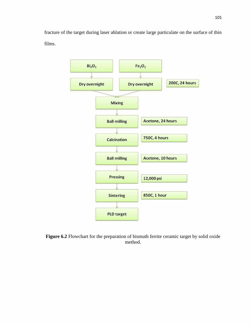
101
fracture of the target during laser ablation or create large particulate on the surface of thin
films.
Figure 6.2 Flowchart for the preparation of bismuth ferrite ceramic target by solid oxide
method.

102
Table 6.1 Weight of raw materials for a 100 g batch of BiFeO3
Composition BFO
Precursor Weight (grams)
Bi2O3 74.4767
Fe2O3 25.5241
Table 6.2 Weight of raw materials for a 100 g batch of
0.6BiFeO3-0.4(Bi0.5K0.5)TiO3
Composition BFO-BKT
Precursor Weight (grams)
Bi2O3 67.6145
Fe2O3 17.3792
K2CO3 5.0138
TiO2 11.5890
Table 6.3 Weight of raw materials for a 100 g batch of 0.88(Bi0.5Na0.5)TiO3-
0.08(Bi0.5K0.5)TiO3-0.04BaTiO3
Composition BNT-BKT-BT
Precursor Weight (grams)
Bi2O3 52.4149
Na2CO3 10.9291
K2CO3 1.2956
TiO2 37.4327
BaCO3 2.5747

103
6.2.2 Laser deposition system
Pulsed laser deposition technique is based on the interaction of high-powered
nanosecond Excimer-laser pulses with bulk targets resulting in evaporation, plasma
formation, and subsequent deposition of thin films. A KrF excimer (Lamda Physik) laser
was used for depositing BFO-based thin films. The KrF excimer laser had a wavelength
of 248 nm and a pulse length ranging of 30 nsec. The laser beam was focused onto the
prepared ceramic target, which was at an angle of 45◦ respect to the beam. The operating
frequency was in the range from 5 to 10 Hz. The laser fluency was varied by placing
attenuation lenses between the lasers and focusing lenses. The substrate was attached to a
substrate heater block with Ag paint. The target to substrate distance was kept at 6.4 cm.
Thin film deposition was carried out in oxygen ambient. The chamber was first pump
using a turbo pump backed by a roughing pump and the substrate was heated to
deposition temperature. The oxygen gas was introduced through a leak valve followed by
deposition. A schematic of the PLD system and Standard Operational Procedure is
shown.
Figure 6.3 Schematic diagram of the deposition system used for laser ablation.

104
6.2.3 Standard procedure
I. Preparation of the instruments
1. Laser chiller, Laser, and the two mechanical pumps are first turned on and warm up for
a few minutes. The mechanical pumps are turn on one at a time to prevent the current
overflow and fuse break. The chiller must be keep on when the laser and/or turbo pump
are running and the water pressure must not exceed 25 psi.
2. Remove the heater flange by removing the bolts and increasing pressure inside the
chamber to push the flange outward.
II. Substrate preparation and installation
3. Clean two small beakers and a pair of tweezers using methanol.
4. Remove the substrates from packaging using Teflon tweezers and put in acetone for 1-
2 minutes. Rinse the substrates in acetone and then in methanol.
5. While the substrate is soak in methanol, vent the chamber with oxygen (set pressure at
10 psi) through the backfill valve with the shutter closed on the substrate heater before
removing the heater flange from the chamber. Remove the heater and immediately
replaced with the blank flange.
6. Rinse the substrate with methanol, then de-ionized water, and finally clean with
compressed air/nitrogen.
7. Apply a small drop of silver paint on the heater block and place the substrate carefully
on the drop of paint and allow the paint to flow to the edges.
8. To dry the solver paint, turn the heater and increase the temperature to 150o
C which
could be part of the heating up program to the final deposition temperature. Place the
heater flange back into the chamber.

105
III. Base Pressure Pump-down
9. Open the right angle valve to pump #2 (roughing pump directly connected to chamber)
to begin the pump-down sequence and raise the shutter.
10. Continue to run the heater program to deposition temperature while the roughing
pump is evacuating the chamber.
11. At approximately 50 mTorr oxygen is introduce into the system to flush out
contaminants. This is repeated several times to ensure a better and faster pump-down.
12. The right angle valve to pump #1 is then opened to rough out the turbo-pump while
the heater reaches the desired temperature.
13. Once the pressure on Convectron gauge is below 20 mTorr, start the turbo-pump.
14. Close the right angle valve to pump #2, and open the gate valve to switch to the high
vacuum turbo-pump.
15. Allow the system to pump-down for 1.5 hours at minimum, or until the pressure is in
the range of 5 to 8 x 10⁻⁶
Torr.
IV. Oxygen Pre-anneal
16. Turn the switch on the MKS oxygen controller to AUTO and close the gate valve
immediately. Turn on the right angle valve to pump #2 by two turns using the screw on
the handle to judge to stabilize at the desired pressure. Shut off the turbo-pump and close
the right angle valve to pump # to isolate the turbo. Vent the turbo-pump by attaching the
plastic tube to nitrogen cylinder and let the nitrogen into the turbo-pump for 10 seconds.
17. Adjust the pressure on MKS controller to the desired value. Allow the substrate to
equilibrate and burn off organic residue for a minimum of 1 hour before film deposition.
106
V. Film Deposition
18. Turn on the laser to allow the pulse energy to stabilize. Using the laser power meter
in front of the beam, measure the power output for a 40 second trend to ensure the
stability. Turn off the laser beam.
19. Un-cover the lens assembly, laser port, and close the shutter on the heater flange.
Select the target and start the target rotation.
20. Open the beam stop to begin the film deposition for the predetermined time. Turn on
the laser.
21. After deposition for the desired time, stop the laser using first the beam stop and then
the keypad to stop the deposition.
22. Close the right angle valve to pump #2, turn the switch on the MKS controller to
CLOSE, and stop the target rotation.
VI. Post-deposition anneal
23. Shut off the heater or allow it to continue with the cool down/annealing program.
24. Fill the chamber with 1 atm oxygen at the beginning of the annealing segment.
25. After the annealing procedure the heater automatically switch off and reset.
VII. Cooling and Shut-down
26. Shut down all equipments if not continuing with another film/layer (Convectron and
turbo-pump controller) deposition.
107
6.2.4 Deposition of bottom electrode
A commercial SrRuO3 (SRO) target with purity 99.9+ % purchased from Super
Conductor Materials Inc., Suffern, NY was employed to deposit a bottom electrode on a
(001)-SrTiO3 (STO) substrate. Deposition of the SRO was following the same procedure
described in previous section. SRO was deposited at a substrate temperature of 800 °C,
150 mTorr oxygen pressure, 200 mJ laser energy, 5 Hz laser repetition rate, and
deposition rate of 40 minutes/100 nm. Following the deposition, the SRO layer was
annealed in the PLD chamber at 650 °C for 1 hour under 1 atm oxygen pressure and then
cooled to room temperature
6.2.5 Deposition of top electrode
Prior to deposition of top electrodes, the surface of the deposited film was cleaned
using nitrogen/air, upon removal of the sample from the PLD chamber. Gold top
electrodes were deposited using DC sputtering technique (EMS150T ES) at room
temperature. Electrodes were patterned using a shadow mask (Stencils Unlimited Inc.,
Lake Oswego, OR) with circular patterns of 200 μm diameter mounted on top of the
sample. The chamber was first evacuated once the pressure inside the chamber reaches 10-
5 Torr. Then Argon was allowed to flow in the chamber keeping with the pressure at 5 x
10-5
Torr. The deposition was performed for 5 minutes.

108
6.3 Bismuth ferrite based thin films
6.3.1 Bismuth ferrite
BFO ceramic target was prepared as previously explained in Section 6.2.1, following
by thin film deposition described in Section 6.2.3. Deposition parameters for BFO
composition were set as follows: substrate temperature of 750 °C, 150 mJ laser energy,
10 Hz repetition rate, oxygen background pressure of 20 mTorr, and 90 minutes/500 nm.
Figure 6.4a present the surface morphology of BFO thin film sample deposited at
mentioned conditions. It is clear that that BFO film consist of block-type hills and porous
microstructure. Similar features have been reported for bismuth ferrite thin films
deposited at oxygen partial pressure lower than 50 mTorr with similar degree of
roughness 10
. The BFO surface roughness and the grain size dramatically depend on the
oxygen partial pressure 10,11
, but it could be related to other parameters such as substrate
temperature, and deposition rate. It is found that 15% La doping results in improvement
of the surface morphology as shown in Figure 6.4b. Note: The electrical properties of
BFO-La doped thin films showed poor hysteresis loop similar to pure BFO, and this
specific composition is not part of this thesis.
XRD in Figure 6.5 revealed the structure and phase of the as grown for pure BFO
films. The sample was scanned in the 2theta range of 20 - 60◦. Only (100) diffraction
peaks corresponding to the BFO perovskite phase were detected for BFO films,
indicating the preferred orientation with no trace of impurities phases.

109
Figure 6.4 FESEM surface image of (a) BFO (inset: BFO cross section), and (b) BFO-La
doped thin film.
Figure 6.5 X-ray diffraction pattern for pure BFO thin film.
Figure 6.6 shows the polarization-electric field hysteresis loop measured at room
temperature and a frequency of 1 kHz. For an electric field of 200 kV/cm the polarization
is low compared to reported values by Wang et al 8 and its banana-like shape is indicative
of a strongly resistive contribution. Despite that BFO-La doped exhibited higher quality
surface morphology compared to un-doped samples (Figure 6.4); similar P-E loop was
20 25 30 35 40 45 50 55 60
SRO (002)
STO (002)
In
ten
sit
y (
a.u
)
STO (001)
Film (002)Film (001)
2-Theta (deg)

110
observed due to the high leakage current which is the main problem of BFO thin films.
The main reason for the leakage current at room temperature has been attributed to
oxygen vacancies. Such vacancies could be a result of a charge imbalance in the BFO
composition.
Figure 6.6 Polarization-Electric Field (P-E) hysteresis loop for single layer bismuth
ferrite thin film measured at 1 kHz and room temperature.
Therefore, in order to reduce the leakage current and improve the quality of films and
ferroelectric behavior two approaches are addressed in the following sections: first, using
target with compositions of BFO-BKT, and second, fabrication of bi-layered thin film of
BFO/BNT-BKT-BT. Such approaches are expected to suppress the formation of oxygen
vacancies and minimize the leakage current.
-200 -100 0 100 200
-4
-2
0
2
4
P
ola
riza
tio
n (C
.cm
2)
Electric field (kV/cm)

111
6.3.2 Effects of oxygen pressure on 0.6BiFeO3-0.4(Bi0.5K0.5)TiO3 thin
films
A BFO-BKT ceramic target was prepared as previously explained in Section 6.2.1,
following by thin film deposition described in Section 6.2.3. Deposition parameters for
BFO-BKT sample were set as follows: substrate temperature of 800 °C, 170 mJ laser
energy, 10 Hz repetition rate, for 90 minutes. The oxygen background pressure for BFO-
BKT thin films was varied in a range of 300 to 500 mTorr while other parameters were
kept fixed. The ferroelectric, dielectric, and leakage current were characterized as a
function of oxygen pressure.
Two-theta XRD spectrum for BFO-BKT thin films grown under different oxygen
pressures are shown in Figure 6.7. The XRD patterns show that a single perovskite phase
has been formed for sample prepared at all oxygen partial pressure. Peak integration
parameters for the h00, h = 2, and 4 peak profile from 2-theta versus intensity plots
shown in Table 6.4 reveals that the (200) peak has shifted toward a lower angle for 300
mTorr. Considering the film thickness of ~ 600 nm, the peak shift can’t be related to
induce strain by the lattice mismatch between the film and the substrate. At this thickness
the film is considered to be strain relieve. Therefore, the peak shift could be related to
changes in film compositions which is confirmed by RBS results.

112
Figure 6.7 X-ray diffraction pattern for BFO-BKT thin films deposited at (a-b) 300
mTorr, (b-c) 400 mTorr, and (c-d) 500 mtorr. The left side images (a, c, d) are for 200,
and right side images (b, d, e) are for 400 integration.

113
Table 6.4 Peak integration parameters for (200) peak profiles
BFO-BKT thin film 2-theta d-spacing (Å) FWHM
300mtorr (200) 46.435 1.9535 0.186
400mtorr (200) 46.447 1.9535 0.167
500mtorr (200) 46.504 1.9512 0.195
Figure 6.8 shows the field emission SEM images of surface and cross section for
BFO-BKT films grown under different oxygen partial pressure. Firstly, it was observed
that surface and cross section images of thin films deposited under different oxygen
pressure is uniform, dense, and crack free. Second, there are some obvious particulates in
samples deposited at 300 and 400 mTorr oxygen partial pressure. In this case the thin
film surface does not appear to change dramatically as a function of oxygen pressure. The
SRO bottom electrode and BFO-BKT film thickness was measured from the cross image
to be approximately 100 and 600 nm respectively.
Rutherford Backscattering Spectrometry (RBS) results for BFO-BKT thin films
deposited under different oxygen pressure are shown in Figure 6.9. The peaks for K, Fe,
and Ti overlapped with Bi peak and can’t be clearly identified in the spectra. Such
overlapping is due to close atomic numbers. Comparing RBS spectrum for different thin
films, the simulated data is well fitted to the experimental results. The main effect of
varying the oxygen pressure down to 300 mTorr causes the slope of Bi narrowing
towards lighter elements. The RBS results indicate that the films, within the detection
limit are free of impurities. The Bi/Fe ratio is shown in Table 6.5. According to the

114
simulation, the Bi/Fe ratio can go down as low as 1.16 without any Fe2O3 formation
according to XRD results.
The calculated thickness according to RBS results for samples deposited at 300 and
400 mTorr is in agreement with SEM measurements of ~ 600 nm.
Table 6.5 Bi/Fe ratio according to RBS simulation
Stoichiometry 300 mTorr 400 mTorr 500 mTorr
Bi/Fe ratio 1.33 1.26 1.18 1.16
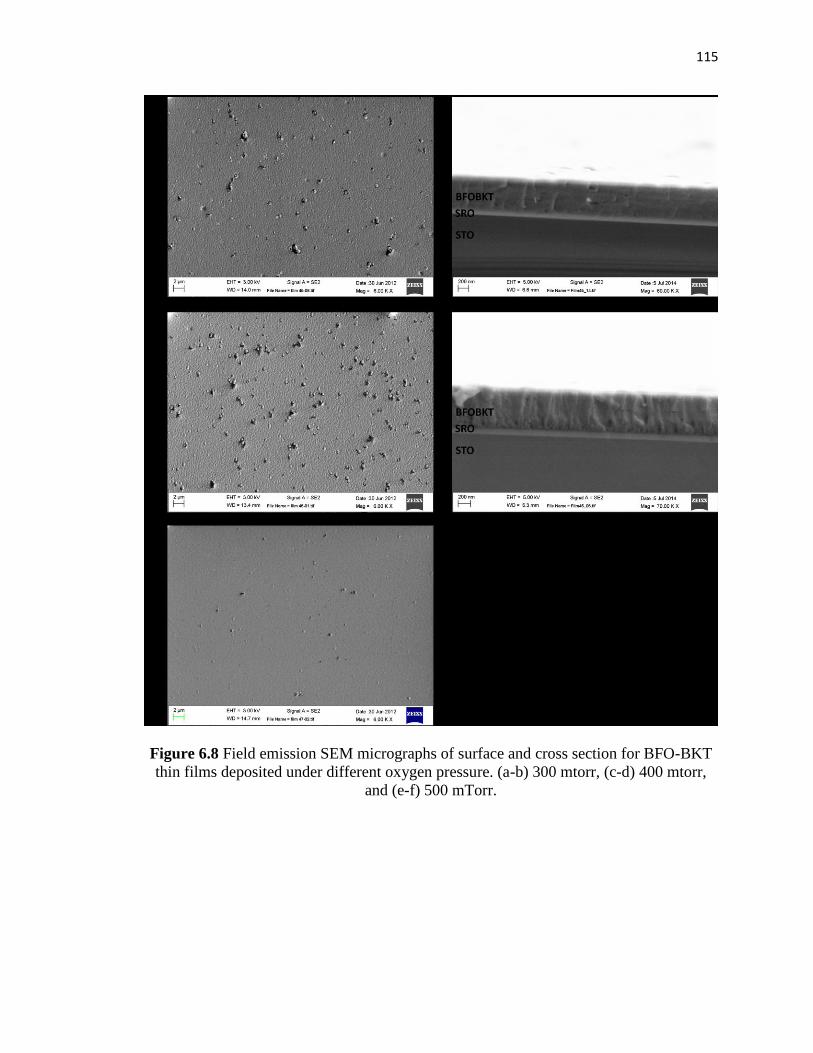
115
Figure 6.8 Field emission SEM micrographs of surface and cross section for BFO-BKT
thin films deposited under different oxygen pressure. (a-b) 300 mtorr, (c-d) 400 mtorr,
and (e-f) 500 mTorr.

116
Figure 6.9 RBS spectrum for BFO-BKT thin film deposited at different oxygen pressure.

117
Polarization-electric (P-E) field hysteresis and leakage current measurements were
performed on BFO-BKT thin films deposited under different oxygen partial pressure.
Ferroelectric measurements were done at room temperature at 1 kHz. Figure 6.10 shows
the hysteresis loop and leakage current results. The BFO-BKT thin films show a well-
shape ferroelectric hysteresis loop with no leakage current component in contrast with
pure BFO thin films in Section 6.3. P-E hysteresis loops (Figure 6.10a) show remnant
polarizations of 2Pr = 33.2, 19.0 and 16.6 µC/cm2 and coercive fields of 2EC = 200, 80
and 80 kV/cm for films deposited at oxygen partial pressures of 300, 400 and 500 mTorr,
respectively. The remnant polarization and coercive field are higher for thin films
deposited at lower oxygen pressure of 300 mTorr. As discussed in the introduction and
background sections, bismuth is major contributor to the spontaneous polarization values
in BFO. Correlating the composition results from RBS presented in Table 6.4 to the
change in remnant polarization values, it is not surprisingly the canting of hysteresis loop
for thin films deposited at 400 and 500 mTorr. When more Bi vacancies are introduced
the gradual canting in the ferroelectric loop is expected.
Figure 6.10b shows the leakage current density of the BFO-BKT thin films as a
function of electric field. It was observed that the leakage current is very sensitive to
oxygen partial pressure during the deposition. The leakage current for thin films
deposited at 300 mTorr is suppressed by four orders of magnitude compared to the thin
films grown at higher oxygen pressure. For thin films deposited at 400 and 500 mtorr the
leakage current exhibited an abrupt increase with the applied field above100 kV/cm while
samples deposited at 300 mTorr showed a more asymmetric behavior. Similar trend is
observed for pure BFO thin films grown by PLD in an oxygen partial pressure range of

118
150 to 10 mTorr 10
. However, the leakage current density is higher (10-3
A.cm-2
) than
BFO-BKT thin films (10-5
A.cm-2
) at an applied electric field of 150 kV/cm reported in
this investigation.
The remnant polarization values for other BFO based solid solution thin films such
as: 0.70BiFeO3-0.3(Bi0.5Na0.5)TiO3 exhibited higher values of 2Pr and 2EC of 52 µC/cm2
and 560 kV/cm respectively 1. Such reported ferroelectric measurements by Hieno were
carried out at -190 ◦C. Wu et al reported high polarization values for 0.95BiFeO3–
0.05(Bi0.50Na0.5)TiO3 [100] oriented thin films as 2Pr of 118.2 µC/cm2
12. Polarization
and leakage current density values for different BFO based solid solution reported by
other groups are shown in Table 6.6.
Table 6.6 Ferroelectric values for BFO based thin film solid solution.
Composition
Deposition
method
Measurements
Conditions
2Pr (µC/cm2) JSC (A/cm
2)
@ 200 kV/cm
0.7BFO-0.3BNT 1 Sol-gel -190 C 52 10
-2
0.95BFO-0.05BNT 12
RF Sputtering RT, 1 kHz 118.2 10-5
BFO-BCO 13
Sol-gel RT, 5 kHz 40 10-6
0.6BLFO-0.40PZT3 RF Sputtering RT, 5 kHz 122.6 -
0.67BFO-0.33BaTO 14
PLD (0.25mbar) RT, 1 kHz 20* -
0.8BFO-0.2BaT 15
PLD (0.067mbar) RT, 10 kHz 38 -
0.6BFO-0.4BKT
This work
PLD (0.40mbar) RT, 1 kHz 33.2 10-5
(*) Hysteresis loop not saturated
119
The leakage behavior in BFO depends on the phase purity, grain size, and defects
such as oxygen vacancy, and Fe3+
/Fe2+
ions. The oxygen vacancy plays an important role
and is described by the following reaction:
(6.1)
or alternatively the reduction of Fe3+
to Fe2+
that occurs to compensate the space charge:
(6.2)
The oxygen vacancies formed during the thin film growth cause part of the Fe3+
to reduce
and become Fe2+
. The Fe2+
ions are responsible for the high leakage of BFO and the
oxygen vacancies act as a space charge, and causes strong domain pinning. Domain
pinning creates a mechanical barrier against domain wall and interferes with its
movement. An increase in the concentration of oxygen vacancies defects results in a
decrease in the remnant polarization 16
, and increase coercive field.
The dielectric behavior of the BFO-BKT films was examined in terms of the relative
permittivity, r, and the dissipation factor (tan ) as a function of frequency at room
temperature for samples grown under different oxygen partial pressure. Figure 6.11a
shows that the films deposited at 500 mTorr have a relatively high dielectric constant at 1
kHz. The dielectric constant for thin films deposited at 300 and 400 mTorr show lower
value of 400but has similar trend vs. frequency. The dielectric constant is quite stable
over the investigated frequency range. Figure 6.11b shows that the thin films deposited at
lower oxygen partial pressure (300 mTorr) have higher dielectric loss compared to those
deposited at 400 and 500 mTorr. The figure also shows the presence of a relaxation
regime for samples deposited at 500 mTorr around 100 kHz.

120
Figure 6.10 (a) Polarization-Electric field (P-E) loops and (b) leakage current
characteristics for BFO-BKT thin films deposited in a range of oxygen partial pressure of
300 – 500 mTorr.

121
Figure 6.11 Dielectric properties of BFO-BKT thin films deposited in a range of oxygen
partial pressure of 300 – 500 mTorr (a) relative dielectric constant, and (b) dielectric loss.
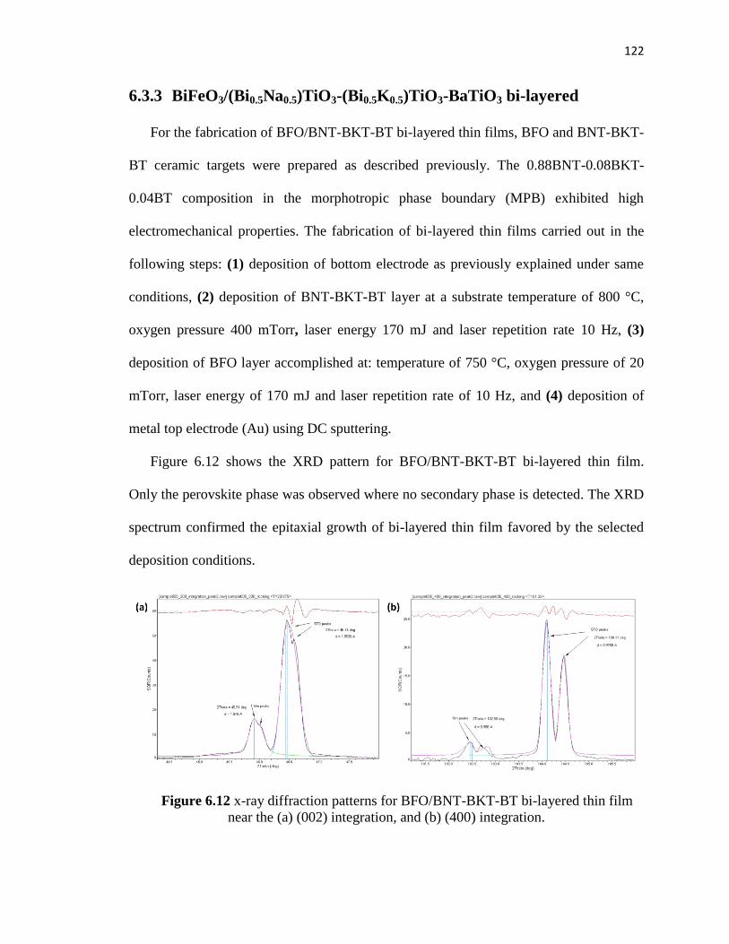
122
6.3.3 BiFeO3/(Bi0.5Na0.5)TiO3-(Bi0.5K0.5)TiO3-BaTiO3 bi-layered
For the fabrication of BFO/BNT-BKT-BT bi-layered thin films, BFO and BNT-BKT-
BT ceramic targets were prepared as described previously. The 0.88BNT-0.08BKT-
0.04BT composition in the morphotropic phase boundary (MPB) exhibited high
electromechanical properties. The fabrication of bi-layered thin films carried out in the
following steps: (1) deposition of bottom electrode as previously explained under same
conditions, (2) deposition of BNT-BKT-BT layer at a substrate temperature of 800 °C,
oxygen pressure 400 mTorr, laser energy 170 mJ and laser repetition rate 10 Hz, (3)
deposition of BFO layer accomplished at: temperature of 750 °C, oxygen pressure of 20
mTorr, laser energy of 170 mJ and laser repetition rate of 10 Hz, and (4) deposition of
metal top electrode (Au) using DC sputtering.
Figure 6.12 shows the XRD pattern for BFO/BNT-BKT-BT bi-layered thin film.
Only the perovskite phase was observed where no secondary phase is detected. The XRD
spectrum confirmed the epitaxial growth of bi-layered thin film favored by the selected
deposition conditions.
Figure 6.12 x-ray diffraction patterns for BFO/BNT-BKT-BT bi-layered thin film
near the (a) (002) integration, and (b) (400) integration.

123
FESEM image of surface morphology for bi-layered is shown in Figure 6.13. The top
layer is the BFO thin film while the BNT-BKT-BT is beneath. The surface appearance is
similar as observed for pure BFO single layer thin film in Figure 6.4a. Similar surface
characteristics in BFO/BFMO bi-layered microstructure grown by RF sputtering have
been reported by Wu et al 17
. BNT-BKT-BT layer is expected to be smooth, uniform,
crack, and pinholes free as found previously 11
.
Figure 6.13 FESEM surface image of BFO/BNT-BKT-BT bi-layered.
NOTE: Top layer is BFO.
Hysteresis loop for bi-layered BFO/BNT-BKT-BT thin film in Figure 6.14
demonstrated an improved ferroelectric behavior compared to BFO single layer in Figure
6.6. As can be observed in Figure 6.14a, the P-E hysteresis loop showed a remnant
polarization of 2Pr = 44.0 µC.cm-2
and a coercive field of 2Ec = 142 kV.cm-1
. Applying
higher voltages to the film resulted in rounded P-E loop which was an indication of high
leakage current. Figure 6.14b show the leakage current for single layer BFO, BNT-BKT-
BT, and bi-layered BFO/BNT-BKT-BT thin films. Multilayer films showed lower

124
leakage current compared with pure BFO, but higher than BNT-BKT-BT. Multilayer thin
films causes an increase in the leakage current due to the defects developed at the
interface between the layers.
The dielectric constant and dielectric loss as a function of frequency for BFO/BNT-
BKT-BT bi-layered and BFO single layer thin films are shown in Figure 6.15. Abazari et
al reported a dielectric constant of 750 at 1 kHz for BNT-BKT-BT thin films 18
.
Considering a series connection between BFO and BNT-BKT-BT layers, the equivalent
dielectric constant can be calculated using equation 6.3 for bi-layered or multilayer
structure which is not in agreement with the obtained experimental results in Figure
6.15a. The dielectric loss values for BFO and BFO/BNT-BKT-BT thin films are similar
regardless of the introduction of BNT-BKT-BT layer, confirming the low free movable
charge density existing in the BFO films 19
. There is noticeable increase in the dielectric
loss for higher frequencies range corresponding to a decrease in the dielectric constant
values.
(6.3)
Some factors that contribute to the improved ferroelectric properties of BFO/BNT-BKT-
BT bi-layered thin films in this investigation could be: (1) Reduction of leakage which
resulted from introducing of BNT-BKT-BT. (2) The interface coupling between BFO and
BNT-BKT-BT should partly enhance the remnant polarization. It is necessary to consider
further study the space charge developed at the interface between BFO and BNT-BKT-
BT which may bring some complications 4. The presence of space charges at the
interface has played an important role in the overall ferroelectric behavior of BFO/BNT-
BKT-BT thin film.

125
Figure 6.14 (a) P-E loop for BFO/BNT-BKT-BT bi-layered thin film, and (b) leakage
current characteristics for BFO, BNT-BKT-BT, and BFO/BNT-BKT-BT thin films.
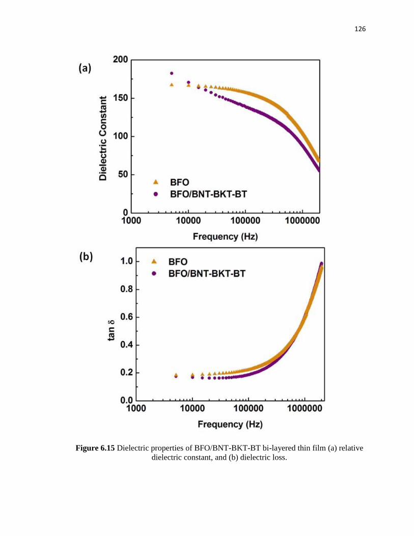
126
Figure 6.15 Dielectric properties of BFO/BNT-BKT-BT bi-layered thin film (a) relative
dielectric constant, and (b) dielectric loss.
127
6.4 Summary
The fabrication and characterization of BFO-based solid solution and bi-layered thin
films have been studied. The thin films were deposited by PLD, and its phase, crystalline
structure, surface morphology, composition and ferroelectric properties were
characterized. Pure bismuth ferrite thin film showed undesirable ferroelectric properties
with high leakage current which correlates with the porous microstructure.
The effect of oxygen background pressure was studied on the fabrication of BFO-
BKT solid solution thin films with the objective to improve the ferroelectric properties of
BFO. BFO-BKT optimum properties were obtained at 300 mTorr oxygen partial pressure
with a remnant polarization of 16.2 C/cm2, and minimum leakage current of 10
-4 A/cm
2.
The leakage current was suppressed by four orders of magnitude compared to thin films
deposited at 500 mTorr. Thin films exhibited better crystallinity and optimum Bi/Fe ratio
in for samples deposited at 300 mTorr which correlate with the properties enhancement.
As a second approach to improve the properties of BFO, a bi-layered design was also
studied. BFO/BNT-BKT-BT bi-layered was deposited also by PLD. The surface
microstructure studied by FESEM exhibited similar characteristics to pure BFO.
However, the BNT-BKT-BT layer beneath BFO promotes improvement ferroelectric
properties and leakage current. Bi-layered thin film exhibited remnant polarization values
of 22.0 C.cm-2
and leakage current of 2.2 x 10⁻⁴
A.cm-2
at 100 kV.cm-1
.
The results showed that BFO-BKT and bi-layered BFO/BNT-BKT-BT thin films
approaches effectively enhance ferroelectric and electrical properties pure BFO thin
films.
128
6.5 References
1. Hieno, A., Sakamoto, W., Moriya, M. & Yogo, T. Synthesis of BiFeO3--
Bi0.5Na0.5TiO3 Thin Films by Chemical Solution Deposition and Their Properties. Jpn.
J. Appl. Phys. 50, (2011).
2. Achenbach, G. D., James, W. J. & Gerson, R. Preparation of Single-Phase
Polycrystalline BiFeO3. J. Am. Ceram. Soc. 50, 437–437 (1967).
3. Wu, J., Zhang, B. & Wang, X. Bismuth ferrite composite thin films. Appl. Phys. A
111, 1017–1020 (2013).
4. Wu, J., Kang, G., Liu, H. & Wang, J. Ferromagnetic, ferroelectric, and fatigue
behavior of (111)-oriented BiFeO3/(Bi1/2Na1/2)TiO3 lead-free bilayered thin films.
Appl. Phys. Lett. 94, 172906 (2009).
5. Ihlefeld, J. F. et al. Adsorption-controlled molecular-beam epitaxial growth of
BiFeO3. Appl. Phys. Lett. 91, 071922–071922–3 (2007).
6. J. F. Ihlefeld, N. J. P. Optical band gap of BiFeO3 grown by molecular-beam
epitaxy. Appl. Phys. Lett. - APPL PHYS LETT 92, 2908–142908 (2008).
7. Wang, C. et al. Leakage current of multiferroic (Bi0.6Tb0.3La0.1)FeO3 thin films
grown at various oxygen pressures by pulsed laser deposition and annealing effect. J.
Appl. Phys. 99, 054104 (2006).
8. Wang, J. et al. Epitaxial BiFeO3 Multiferroic Thin Film Heterostructures. Science
299, 1719–1722 (2003).
9. Ahadi, K., Mahdavi, S. M., Nemati, A. & Kianinia, M. Photoconductivity and
diode effect in Bi rich multiferroic BiFeO3 thin films grown by pulsed-laser deposition.
J. Mater. Sci. Mater. Electron. 22, 815–820 (2011).
10. Yun, K. Y. et al. Structural and multiferroic properties of BiFeO3 thin films at
room temperature. J. Appl. Phys. 96, 3399–3403 (2004).
11. Hejazi, M., Jadidian, B. & Safari, A. Lead-free (Bi0.5Na0.5)TiO3-based thin
films by the pulsed laser deposition process. IEEE Trans. Ultrason. Ferroelectr. Freq.
Control 59, 1855–1863 (2012).
12. Wu, J. & Wang, J. Multiferroic behaviour and orientation dependence of lead-free
(1 − x)BiFeO3–x(Bi0.50Na0.50)TiO3 thin films. J. Phys. Appl. Phys. 42, 195405 (2009).
13. Singh, S. K., Shanthy, S. & Ishiwara, H. Reduced leakage current in BiFeO3-
BiCrO3 nanocomposite films formed by chemical solution deposition. J. Appl. Phys. 108,
4102 (2010).
14. Michael Lorenz, V. V. L. Multiferroic BaTiO3–BiFeO3 composite thin films and
multilayers: strain engineering and magnetoelectric coupling. J. Phys. Appl. Phys. 47,
135303 (2014).
15. Sasaki, T., Hirabayashi, Y., Kobayashi, H. & Sakashita, Y. Effect of Dopant on
Piezoelectric Properties of Lead-Free BiFeO3–BaTiO3 Film. Jpn. J. Appl. Phys. 50,
09NA08 (2011).
16. Noguchi, Y., Miwa, I., Goshima, Y. & Miyayama, M. Defect Control for Large
Remanent Polarization in Bismuth Titanate Ferroelectrics –Doping Effect of Higher-
Valent Cations–. Jpn. J. Appl. Phys. 39, L1259 (2000).
17. Wu, J. et al. Effect of bilayer structure and a SrRuO3 buffer layer on ferroelectric
properties of BiFeO3 thin films. Appl. Phys. A 109, 57–61 (2012).

129
18. Abazari, M., Safari, A., Bharadwaja, S. S. N. & Trolier-McKinstry, S. Dielectric
and piezoelectric properties of lead-free (Bi,Na)TiO3-based thin films. Appl. Phys. Lett.
96, 082903 (2010).
19. Wu, J., Wang, J., Xiao, D. & Zhu, J. Combined effects of bilayer structure and ion
substitutions on bismuth ferrite thin films. J. Appl. Phys. 109, 4101 (2011).
130
7 Bismuth Ferrite Nanofibers by Electrospinning
7.1 Introduction
Bismuth ferrite has attracted extensive research activities because its multiferroic
properties. While investigators are studying the ferroelectric properties from a
fundamental physical and experimental perspective, the understanding of its optical
properties such as band gap, photoconductivity for novel applications is emerging.
Recent investigations on BFO photovoltaics cause a great interest in its novel
multifunctional applications. Bismuth ferrite is a semiconductor material with and optical
band gap between 2.17-2.81 eV which falls in the visible light region.
On the other hand, one dimensional nanostructures, including nanofibers (lateral size
< 100 nm), nanowires (lateral size > 100nm), and nanotubes have received considerable
attention due to their tunable electromechanical, photovoltaic and optoelectronic
properties 1
.
This chapter presents the optimization process to develop bismuth ferrite nanofibers
with different diameter by electrospinning technique. The phase, structure, composition,
morphology, valance state, and electronic properties are characterized. Developed
bismuth ferrite nanofibers have been used to fabricate field effect transistor devices.

131
7.2 Experimental procedure
7.2.1 Electrospinning setup
The electrospinning technique is a simple and yet versatile method to fabricate ultra
thin fibers from a diversity of materials which includes polymers, composites, and
ceramics. 2. Electrospinning is continuous process and therefore suitable for high-volume
production. The electrospinning principal is based on an electrostatic force interaction in
which a high electric field is applied on a droplet of a polymer based solution held by its
surface tension at the tip of a syringe needle 3. The droplet is highly charged and the
induced charges are distributed over its surface. By adjusting the electric field, the shape
of the droplet is distorted and form a conical form known as a “Taylor cone” 4,5
. When
the electric field is high enough to overcome the surface tension of the droplet the
repulsive forces dominates and the liquid emerges from the cone tip as jet (stream). The
jet is accelerated toward the collector and quickly thins and dries as a result of solvent
evaporation and elongation 3. Finally, the solidification occurs at the surface of the
collector or substrate as randomly oriented mat.
Figure 7.1 Schematic for electrospinning setup.
132
The physical characteristics of electrospun nanofibers such as diameter depend on
various parameters which can be grouped in following three categories:
(1) Solution properties (viscosity, concentration, polymer molecular weight, and
surface tension)
(2) Processing conditions (applied voltage, flow rate, spinning distance and needle
diameter), and
(3) ambient conditions (temperature, humidity, and atmosphere pressure) 6.
Different applications require nanofibers with desired characteristics, suggesting the
importance of the process protocol 3. Control over the fiber diameter still is not well
established in experimental procedure. Some empirical observations suggest that the
diameter could be varied by the flow rate. Considering that electrospun nanofibers are
produced from a precursor solution, the dry nanofibers diameter can be controlled with
the solution concentration 7.

133
7.2.2 Standard operation procedure (SOP)
1. Polymer selection:
a. Select a polymer according to the desired specifications such as
biodegradable, thermoplastic, and cross-linkable.
b. Select the appropriate solvent for polymer.
c. Choose a substrate based on your application (glass, metal, plastic or
silicon wafer).
2. Collector selection:
a. Select a collector geometry based on your desired nanofibers
alignment/orientation. Aligned nanofibers can be obtained using rotating
wheels, drums, rods or parallel plates. Random nanofibers can be obtained
in stationary plates.
b. The collector must be conductive and need to be grounded.
3. Approximate entangle concentration:
a. Prepare several precursor solution concentrations which are liquid but do
not form a gel.
b. Start the electrospinning setup.
i. Load the precursor solution onto the syringe
ii. Load the syringe pump and set the pump speed
iii. Ground the collector (20 cm apart from the needle, to start) and
connect to the high voltage wire to the needle.
iv. Fix the substrate with a double sided tape on the collector.
v. Make sure the power supply is set to zero before turning on.

134
vi. Turn ON the power supply and wait to warm up for five minutes.
Note: Safety precautions must be taken when working with high
power supply.
vii. Turn the HV ON and wait to warm up for few minutes.
4. Observe the jet:
i. Ramp the voltage (5kV to start) slowly and watch the drop of the
solution at the end of the needle.
ii. Increase the voltage to obtain a steady solution jet.
Note: If steady solution jet cannot be obtained adjust the solution
concentration, flow rate or distance between the needle and the
collector.
5. Troubleshooting – the jet:
a. Trouble viewing the jet: use a dark matte background.
b. Dripping from the syringe tip: make sure the conductor wire is making
contact and collector is properly connected to ground.
c. Large globs at the syringe tip: swipe the glob away with a paper towel.
Note: Attached the paper towel to a non-conductive stick
d. Oscillating or “wagging” jet: decrease the voltage or increase the distance
between the needle and the collector.
6. Troubleshooting – fiber morphology:
a. Beading: increase solution concentration or the distance between the
needle and the collector.

135
b. Forming ribbons: use a higher concentration of polymer or a solvent with
higher evaporation rate.
c. Porosity: if porous fibers are desired use a high rate evaporating solvent, if
porous fibers are not desired add a small amount of co-solvent that is less
volatile that the major solvent.
d. Alignment: increase the alignment by increasing the speed of rotation tool
(wheel, drum, rods or plates).
7.2.3 Sol gel solution preparation
The preparation of BFO nanofibers involves the following general steps:
(1) preparing the precursor solution
(2) electrospinning to obtain inorganic/organic nanofibers
(3) Heat treatment of the as spun nanofibers to remove the polymer and obtain dense
and crystalline BFO fibers.
The sol gel solution was prepared as follows. The nitrates based solution, referred as
Solution A, was prepared by dissolving Bi(NO3)3.5H2O and Fe(NO3)3.9H2O in a
combination of 2methoxyethanol and glacial acetic acid with 2:1 ratio. The solution was
under constant stirring for one hour at room temperature. Then, a 15 wt% polymer
solution referred as Solution B, was prepared by adding polyvinyl pyrroldine (PVP) with
a molecular weight (MW) of 630,000 to dimethyl formamide (DMF) with a ratio of 1:5
(wt/wt) respectively. The solution was stirred for two hours or until the polymer had
completely dissolved in DMF. To obtain a homogenous distribution of BFO solution into
the polymer, nitrates solution was added drop by drop to polymeric solution while stirring

136
at room temperature. Note: The PVP was added to assist in the fiber formation which
later is removed by heat treatment. In order to prepare nanofibers of different diameter,
solutions with different concentrations in the range of 0.4 - 1.4 M were prepared. Using
an electrospinning apparatus, BFO nanofibers were deposited on Si/SiO2 and quartz
substrates. Electrospinning was conducted at 12 kV with 20 cm separation between the
needle tip and the collector. The obtained nanofibers were dried in a closed furnace at
120 °C for 1 hour, followed by a polymer removal step at 400 °C for 1 hour, and final
crystallization at 550 °C for 2 hours.
7.3 Fabrication and characterization of bismuth ferrite nanofibers
Following SOP described in Section 7.2.2, this section focused in the process
optimization for the development of BFO nanofibers with different diameter. Bismuth
ferrite nanofibers with good physical properties (morphology) have been fabricated
earlier by Baji et al. 1. However, there are no report on the variation of nanofibers
diameter and its effect on the electrical properties. Starting solution parameters such as
polymer, solvent, co-solvent ratio, and raw materials have been obtained from the
literature. To ensure the good morphology and microstructure of the nanofibers, the
apparatus settings such as driving voltage, flow rate, and distance between the collector
and syringe are optimized. Control over the nanofibers diameter is accomplished by
varying the precursor solution concentration. The crystal structure, morphology, grain
size, valance state of the nanofibers were studied.

137
7.3.1 Optimization of processing and solution conditions
A BFO precursor solution of 0.6 M concentration was used to determine the optimum
processing conditions and to achieve a continuous solution jet to result in good fiber
morphology. The collector geometry was selected as a stationary plate which resulted in
randomly deposited nanofibers. The starting distance between the needle and the
collector was initially set to 20 cm. The processing optimization results are summarized
in the following tables.
Table 7.1 Electrospinning processing optimization: Flow rate
Flow rate Troubleshooting the jet
1.0ml/hr Beaded-nanofibers, solution dripping continuously
0.8ml/hr Beaded-nanofibers, solution dripping continuously
0.6ml/hr Beaded-nanofibers, solution dripping at further distance
0.4ml/hr Beaded-nanofibers reduced, droplet stable at the tip
0.2ml/hr Free-beaded nanofibers, droplet stable at the tip *
Table 7.2 Electrospinning processing optimization: Voltage
Voltage Troubleshooting the jet
6 kV Droplet at the needle tip
8 kV Droplet at the needle tip, which slowly deforms and
dripping down
10 kV Drop forms at the needle tip, slowly deforms, and a jet is
ejected. However, the jet is short and discontinuous.
12 kV Drop forms at the needle tip, slowly deforms, and a
continuous jet is occurring. *
14 kV Drop forms at the needle tip, more quickly deforms and
the jet is ejected. The jet is moving from side to side
(“wagging”).
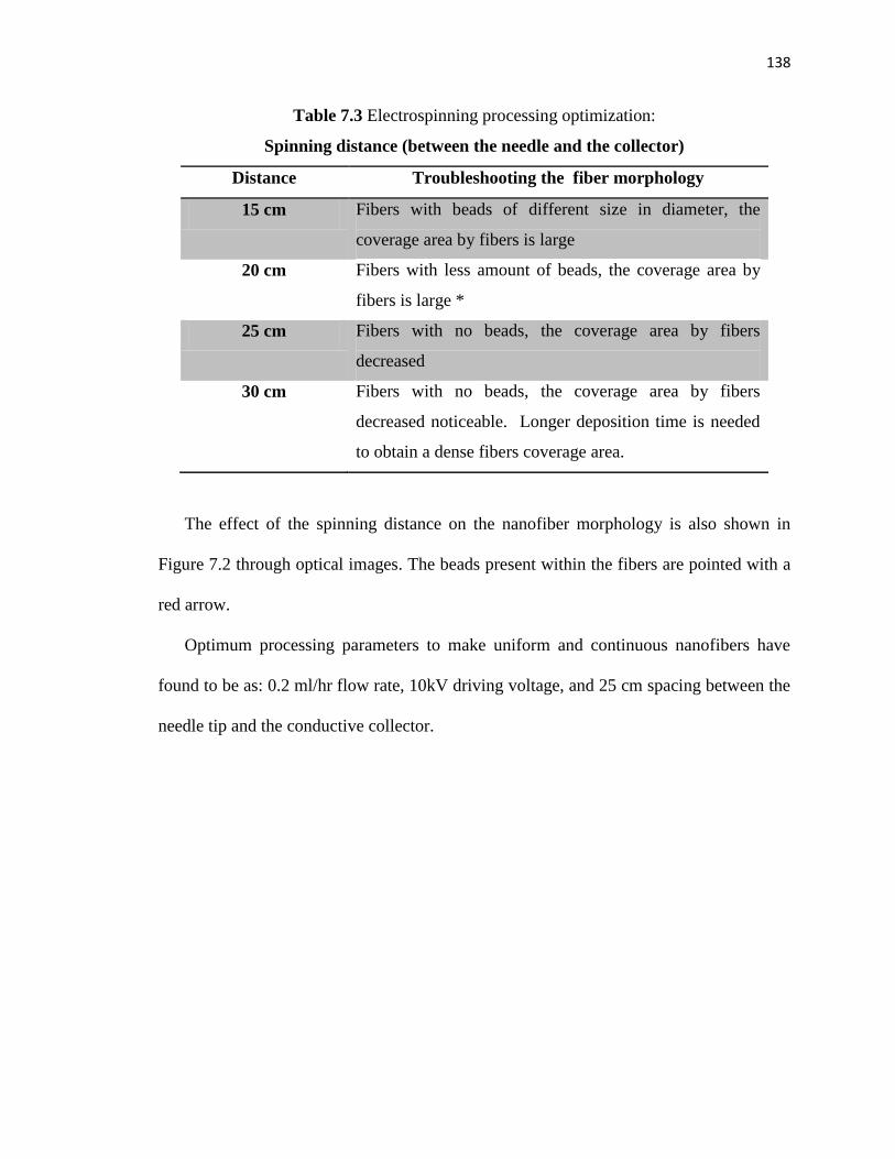
138
Table 7.3 Electrospinning processing optimization:
Spinning distance (between the needle and the collector)
Distance Troubleshooting the fiber morphology
15 cm Fibers with beads of different size in diameter, the
coverage area by fibers is large
20 cm Fibers with less amount of beads, the coverage area by
fibers is large *
25 cm Fibers with no beads, the coverage area by fibers
decreased
30 cm Fibers with no beads, the coverage area by fibers
decreased noticeable. Longer deposition time is needed
to obtain a dense fibers coverage area.
The effect of the spinning distance on the nanofiber morphology is also shown in
Figure 7.2 through optical images. The beads present within the fibers are pointed with a
red arrow.
Optimum processing parameters to make uniform and continuous nanofibers have
found to be as: 0.2 ml/hr flow rate, 10kV driving voltage, and 25 cm spacing between the
needle tip and the conductive collector.
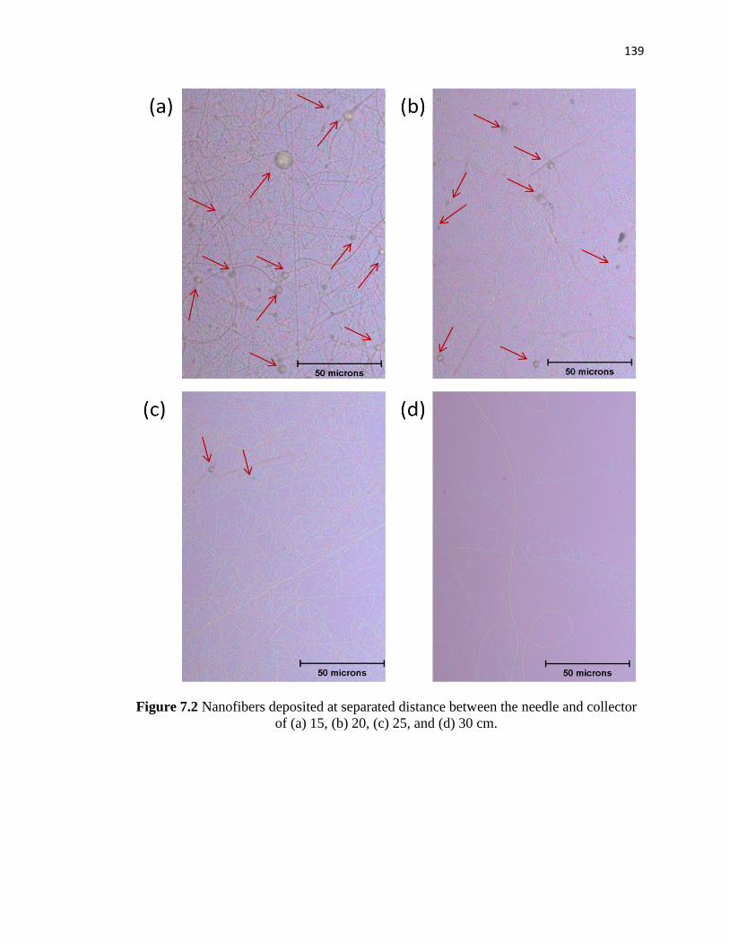
139
Figure 7.2 Nanofibers deposited at separated distance between the needle and collector
of (a) 15, (b) 20, (c) 25, and (d) 30 cm.

140
7.3.2 Characterization of bismuth ferrite nanofibers
It is difficult to perform XRD analysis directly on electrospun nanofibers because of
the low coverage area of nanofibers and high background contribution from the substrate.
Hence, to ensure pure perovskite phase of BFO nanofibers, thin films with thickness of
100 nm were prepared by spinning the same precursor solution batches. The XRD pattern
of the films in Figure 7.3 revealed pure perovskite phase with a rhombohedral structure.
To further confirm the structure and phase of BFO nanofibers, Raman Spectroscopy and
TEM analysis was carry out.
Figure 7.3 X-ray diffraction pattern for a BFO thin film of the same precursor
solution as the nanofibers.
20 30 40 50 60
(220)
(120)
(020)
(111)
(110)
(010)
Inte
nsit
y (
a.u
.)
2theta (deg)

141
For further insight into the lattice properties and spin-phonon mode coupling, Raman
scattering studies have also been carried out on BFO nanofibers. Figure 7.4 shows the
Raman spectra of the nanofibers mat at room temperature. NOTE: A fiber mat is a very
dense area filled with nanofibers in which the substrate is 90% covered. The fiber mat
was prepared under the optimum conditions from a 0.6 M BFO precursor solution with a
deposition time of 2 hours. The rhombohedral (R3c) structure of BFO give rises to 13
Raman actives modes listed as 4A1 + 9E as shown in Table 5.1 8,9
. The observed natural
frequency (cm-1
) of each peak position can be designed to a different Raman active mode.
It appears that several peaks is absent in in Fig 7 spectra based on Raman phonon peaks
in Table 5.1. The absence of some of the Raman peaks may be due to the higher local
stress in the nanofibers as has been discussed by Singh et al 10
.
Figure 7.4 Raman Spectroscopy for 0.6M BFO nanofibers mat.
100 200 300 400 500 600 700 800
56
2 -
A1(T
O)
47
2 -
A1(L
O)
36
3 -
E(T
O)
26
8 -
E(T
O)
21
9 -
A1(L
O)
14
0 -
A1(L
O)
16
6 -
A1(L
O)
88
- E
(L
O)
Ram
an
In
ten
sit
y (
a.u
.)
Wavenumber (cm-1)

142
The Figure 7.5 shows the TEM image for a single BFO nanofiber deposited under
optimum condition with a diameter of 100 nm. TEM results reveal the nanocrystalline
nature of electrospun nanofibers. The d-spacing for the BFO nanofiber from the selective
area diffraction (SAED) pattern in Figure 7.5b corresponding to R3c space group which
is shown in Table 7.4. Raman and TEM results confirmed that BFO nanofibers are well
crystallized with single phase rhombohedral structure.
Figure 7.5 Transmission electron microscope (TEM) image for a 100 nm nanofibers.
(a) surface image, and (b) diffraction pattern

143
Table 7.4 d-spacing for single BFO nanofibers from TEM
d-spacing Standard
Hexagonal (R3c)
d-spacing from this work
0.3968
(012)
0.390
0.2818
(104)
0.274
0.2391
(113)
0.240
0.2311
(202)
0.230
0.2284
(202)
0.221
0.1984
(024)
0.190
0.1618
(214)
0.160
0.1397
(220)
0.135
0.1252
(134)
0.121
0.1195
(226)
0.119
144
7.3.3 Nanofibers with different diameters
Leach et al. reported solution concentration plays an important role on the final grain
size using a similar deposition technique 11
. Solution surface tension and solution
viscosity are also important determining parameters to define the concentrations of
solution and hence surface quality of continuous nanofibers prepared by electrospinning
method 7. Under certain viscosity range, the surface tension plays a dominant rule on the
fiber morphology. Above certain viscosity the production of nanofibers cannot be
possible.
One of the objectives of this research is to fabricate BFO nanofibers with different
diameters. The polymer solution concentration and electrospinning processing parameters
were kept constant (0.2 ml/hr flow rate, 10kV driving voltage, and 20 cm spacing
between the needle tip and the conductive collector) as optimized in Section 7.3.1; and
only BFO nitrates solution concentration was varied between 0.4 and 1.4 M. It was
observed that below 0.4 M concentration there were a combination of fibers and beads,
and the formation of a continuous jet was not obtained for solution concentrations higher
than 1.4 M. For the higher concentration forcing the solution through the syringe needle
was difficult, and the needle clogged. Nanofibers free of beads were obtained from
solution concentrations between 0.4 and 1.4 M. the amount of collected nanofibers per
area also increases as the concentration reach to 1.4 M. The nanofibers morphology and
diameter was analyzed using the SEM. Micrographs for nanofibers of different solution
concentrations are shown in Figure 7.6. The obtained SEM micrographs were utilized to
quantify the nanofibers diameter using the software Image J. It was found that by
increasing the precursor solution concentration the nanofibers diameter increases as
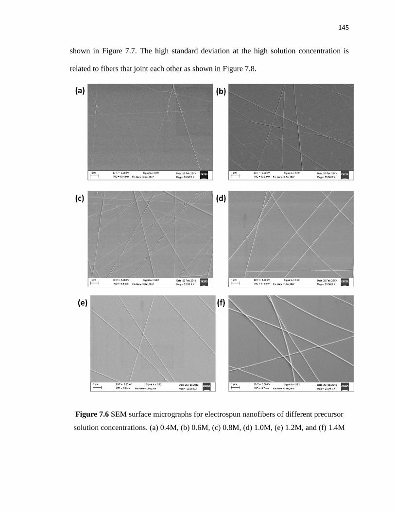
145
shown in Figure 7.7. The high standard deviation at the high solution concentration is
related to fibers that joint each other as shown in Figure 7.8.
Figure 7.6 SEM surface micrographs for electrospun nanofibers of different precursor
solution concentrations. (a) 0.4M, (b) 0.6M, (c) 0.8M, (d) 1.0M, (e) 1.2M, and (f) 1.4M

146
Figure 7.7 Nanofibers diameter as a function of precursor solution concentration.
Figure 7.8 High resolution transmission electron microscope (HRTEM) image of a joint
BFO nanofibers with high solution concentration.
0.4 0.6 0.8 1.0 1.2 1.4
40
80
120
160
Dia
me
ter
(nm
)
Solution Molarity
0. 1 µm0. 1 µm

147
7.3.3.1 Grain size
As previously mentioned electrospun nanofiber consisted of nanograins. The physical
and chemical properties of the nanofibers could be co-related with the size of nanograins.
In this study the grain size as a function of nanofiber diameter was measured with the
TEM and the results are shown in Figure 7.9. The grain size increases sharply up to 60
nm nanofibers diameter and then saturates at higher diameter. There are approximately
seven nanograins in a nanofiber with 40 nm diameter.
Figure 7.9 Average grain size as a function of fiber diameter obtained from TEM.

148
7.3.3.2 Iron valence state
Iron valence state is an important feature in BFO system because it influences the
electrical properties of nanofibers. Electron Energy Loss Spectroscopy (EELS)
experiment was performed on individual nanofibers of different diameters to determine
the valence state of iron. The results in Figure 7.10 show that nanofibers with smaller
diameter (40 nm) are composed mostly of Fe3+
valence state while nanofibers with larger
diameters (80 nm) are mostly composed of Fe2+
valence. The valance state of Fe (3+ and
2+) of the nanofibers with diameter in between the two extreme value have a combination
of Fe2+
and Fe
3+ . For nanostructures, it is energetically unfavorable to create defects in
the core of the particles, then possible surfaces impurities of nanostructure may have
effect on the variation of valence state 12
. The observation of valence state fluctuation can
be due to reduced coordination number of the atoms at the surface of the BFO nanofibers
due to reduced grain size (Figure 7.9). If considering a reduced coordination number, the
electron density around Fe3+
ions on the surface of the nanofibers would be less and
hence the shielding of the iron nucleus is decreased causing the electrons to be pulled
closer 12
. Another reason behind the observation of iron valence fluctuation can be due
organic polymer removal stage. In the process of polymer burn out, organic binders are
thermally removed before completing crystallization. For the incomplete burn out, the
trapped organic residues will be a contamination source and affects the oxidation of the
final sample. On the other hand, if the burn out is carried hastily; defects in the green
samples will form. Considering, different various diameter of the nanofibers, larger
amount of organic polymer must be removed from nanofibers with larger diameters 13
.

149
When removing the organic polymer, oxygen defects maybe created in which inducing
charge balance compensation (Fe3+
to Fe2+
).
Figure 7.10 Fe valence state as a function of fiber diameter obtained from EELS
analysis.
7.3.3.3 Chemical composition
Rutherford Backscattering Spectrometry (RBS) results for BFO nanofibers mat of
1.0, 0.8, and 0.6 M corresponding to different average diameters are shown in Figure 7.11
to 7.13. The peaks for Bi and Fe are clearly indentified in the RBS spectra. The simulated
data is well fitted to the experimental results for nanofibers different diameter. The RBS
results indicate that the nanofibers, within the detection limit are free of impurities. The
composition derived from the simulation was found to be more deficient in iron compare
to stoichiometric composition (BiFeO3), especially for nanofibers prepared with high
molarity.
40 50 60 70 802.0
2.2
2.4
2.6
2.8
3.0
3.2
Fe
va
len
ce
Fiber diameter (nm)
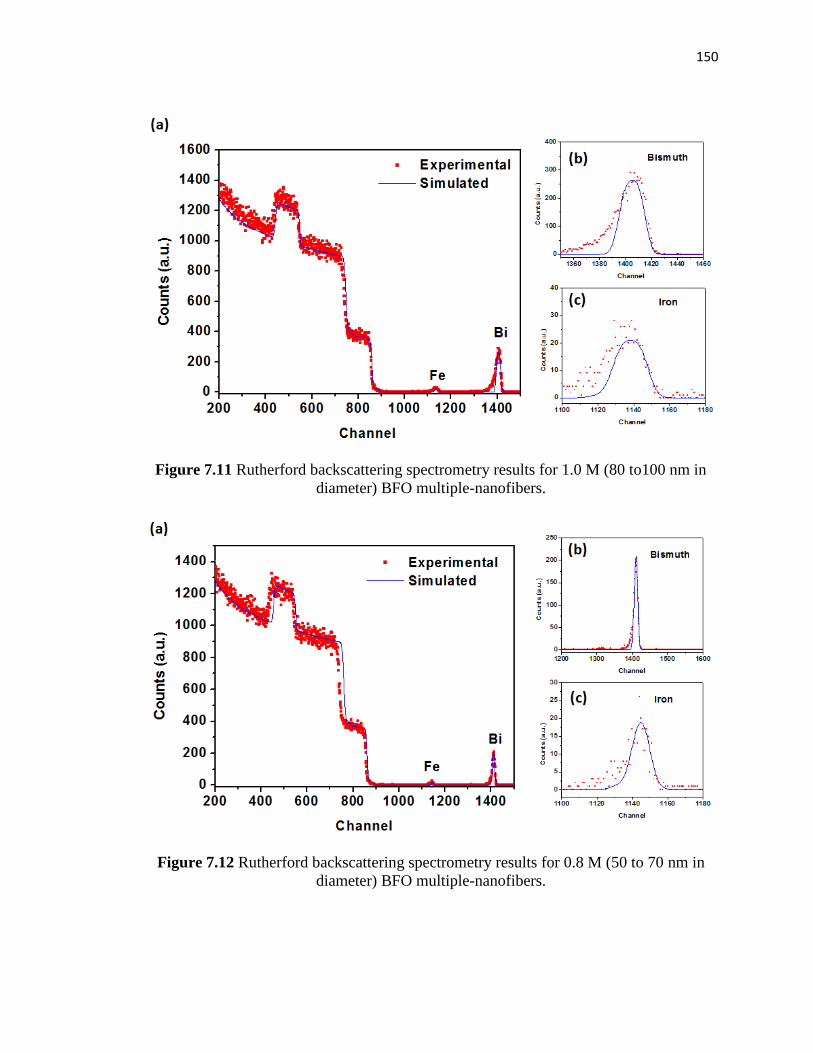
150
Figure 7.11 Rutherford backscattering spectrometry results for 1.0 M (80 to100 nm in
diameter) BFO multiple-nanofibers.
Figure 7.12 Rutherford backscattering spectrometry results for 0.8 M (50 to 70 nm in
diameter) BFO multiple-nanofibers.
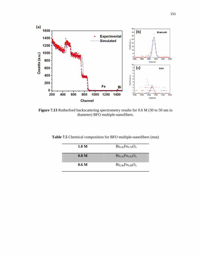
151
Figure 7.13 Rutherford backscattering spectrometry results for 0.6 M (30 to 50 nm in
diameter) BFO multiple-nanofibers.
Table 7.5 Chemical composition for BFO multiple-nanofibers (mat)
1.0 M Bi0.85Fe0.78Ox
0.8 M Bi0.92Fe0.82Ox
0.6 M Bi0.96Fe0.88Ox
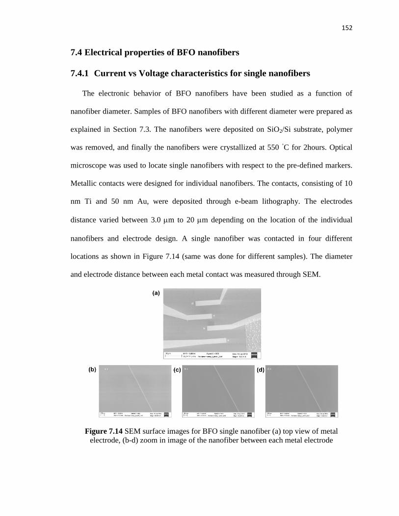
152
7.4 Electrical properties of BFO nanofibers
7.4.1 Current vs Voltage characteristics for single nanofibers
The electronic behavior of BFO nanofibers have been studied as a function of
nanofiber diameter. Samples of BFO nanofibers with different diameter were prepared as
explained in Section 7.3. The nanofibers were deposited on SiO2/Si substrate, polymer
was removed, and finally the nanofibers were crystallized at 550 ◦C for 2hours. Optical
microscope was used to locate single nanofibers with respect to the pre-defined markers.
Metallic contacts were designed for individual nanofibers. The contacts, consisting of 10
nm Ti and 50 nm Au, were deposited through e-beam lithography. The electrodes
distance varied between 3.0 m to 20 m depending on the location of the individual
nanofibers and electrode design. A single nanofiber was contacted in four different
locations as shown in Figure 7.14 (same was done for different samples). The diameter
and electrode distance between each metal contact was measured through SEM.
Figure 7.14 SEM surface images for BFO single nanofiber (a) top view of metal
electrode, (b-d) zoom in image of the nanofiber between each metal electrode
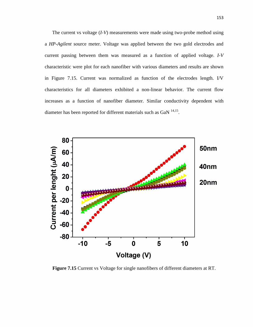
153
The current vs voltage (I-V) measurements were made using two-probe method using
a HP-Agilent source meter. Voltage was applied between the two gold electrodes and
current passing between them was measured as a function of applied voltage. I-V
characteristic were plot for each nanofiber with various diameters and results are shown
in Figure 7.15. Current was normalized as function of the electrodes length. I/V
characteristics for all diameters exhibited a non-linear behavior. The current flow
increases as a function of nanofiber diameter. Similar conductivity dependent with
diameter has been reported for different materials such as GaN 14,15
.
Figure 7.15 Current vs Voltage for single nanofibers of different diameters at RT.

154
7.4.2 Size dependent on the photoconductivity of multiple-nanofibers
The photoconductivity of bismuth ferrite nanofibers mats with different average
diameters was studied. The electrical measurements was carry out using a two-probe
system and a HP-Agilent source meter and a solar simulator with AM 1.5 spectra output
was chosen as the light source. To study the photoresponse a constant voltage (10V) was
applied and the variation in the current was measured upon illumination of the fibers to
light (Figure 7.16).
Figure 7.16 Current vs time at constant voltage (10V) upon illumination
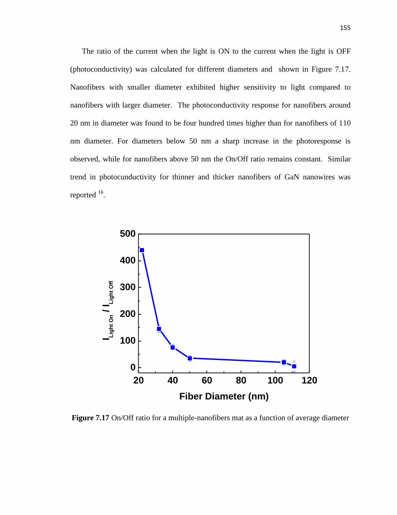
155
The ratio of the current when the light is ON to the current when the light is OFF
(photoconductivity) was calculated for different diameters and shown in Figure 7.17.
Nanofibers with smaller diameter exhibited higher sensitivity to light compared to
nanofibers with larger diameter. The photoconductivity response for nanofibers around
20 nm in diameter was found to be four hundred times higher than for nanofibers of 110
nm diameter. For diameters below 50 nm a sharp increase in the photoresponse is
observed, while for nanofibers above 50 nm the On/Off ratio remains constant. Similar
trend in photocunductivity for thinner and thicker nanofibers of GaN nanowires was
reported 16
.
Figure 7.17 On/Off ratio for a multiple-nanofibers mat as a function of average diameter
20 40 60 80 100 120
0
100
200
300
400
500
I Lig
ht
On /
IL
igh
t O
ff
Fiber Diameter (nm)
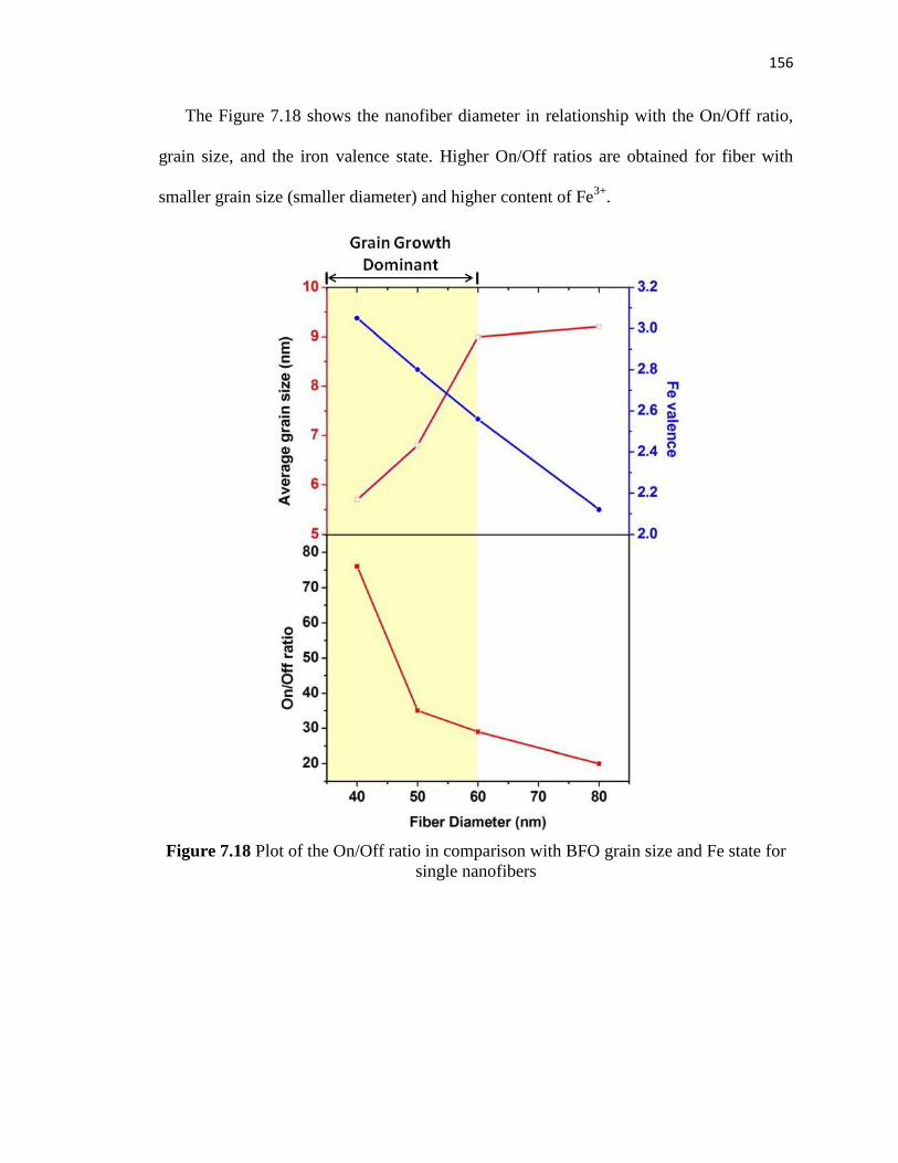
156
The Figure 7.18 shows the nanofiber diameter in relationship with the On/Off ratio,
grain size, and the iron valence state. Higher On/Off ratios are obtained for fiber with
smaller grain size (smaller diameter) and higher content of Fe3+
.
Figure 7.18 Plot of the On/Off ratio in comparison with BFO grain size and Fe state for
single nanofibers

157
Wide band gap materials such as BFO possess high density of surface states within
the band gap 17
. The density of surface states does not influence the optical properties of
bulk materials and thin films; however effectively dominate in one-dimensional
nanostructures due to large surface to volume ratios. The presence of surface states in the
band gap is known to pin the Fermi level position in the semiconductor 16,18
. Therefore,
photons having energy lower than the band gap can be absorbed by the surface states as a
result of faster availability of electronic transitions. Considering the high surface-volume
ratio of the BFO nanofibers, sub-band transitions become dominant for optical
absorption. In the bulk or thin films, the principal behind the reported photovoltaic effect
is the internally generated electric field originated from the ferroelectric domains 19,20
.
Such internal generated electric field is responsible for the separation of photogenerated
carriers on BFO nanofibers. Considering the nanostructure nature of BFO in this
research, in addition to the ferroelectric polarization, there is a significant contribution of
the surface potential.
Due to the Fermi level pinning within the forbidden band, semiconductor nanofibers
exhibit a depletion space charge layer with the extension of the order of the nanofiber
diameter. Conditional to the nanofiber diameter, completely depleted nanofibers or
nanofibers with conducting channels exits. The energy bands at the surface of BFO
nanofibers are bent due to trapped charges or surface defects, thus the resulting surface
potential can separated the photogenerated charge carriers 18
.
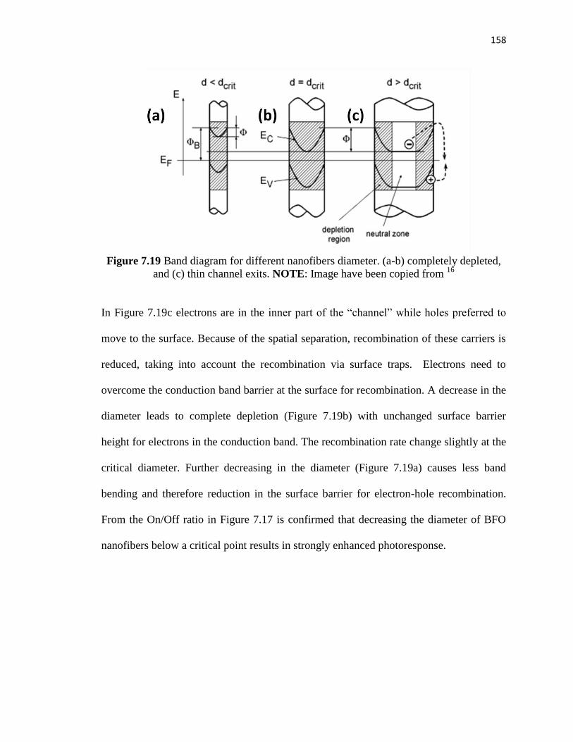
158
Figure 7.19 Band diagram for different nanofibers diameter. (a-b) completely depleted,
and (c) thin channel exits. NOTE: Image have been copied from 16
In Figure 7.19c electrons are in the inner part of the “channel” while holes preferred to
move to the surface. Because of the spatial separation, recombination of these carriers is
reduced, taking into account the recombination via surface traps. Electrons need to
overcome the conduction band barrier at the surface for recombination. A decrease in the
diameter leads to complete depletion (Figure 7.19b) with unchanged surface barrier
height for electrons in the conduction band. The recombination rate change slightly at the
critical diameter. Further decreasing in the diameter (Figure 7.19a) causes less band
bending and therefore reduction in the surface barrier for electron-hole recombination.
From the On/Off ratio in Figure 7.17 is confirmed that decreasing the diameter of BFO
nanofibers below a critical point results in strongly enhanced photoresponse.

159
7.5 Bismuth ferrite field effect transistor devices with single nanofiber
and multiple-nanofibers
Bismuth ferrite nanofibers of ~ 50 nm diameter were prepared from a 0.6 M precursor
solution, deposited on SiO2/Si substrates, and crystallized at 550 ◦C. Using the optical
microscope, areas with single nanofibers and multiple-nanofibers were located in
different samples for device fabrication. The contacts, consisting of (1) 10 nm Ti/50 nm
Au, (2) 20 nm Al2O3, and (3) 10 nm Ti and 50 nm Au were deposited through e-beam
lithography. The aluminum oxide layer is used as top dielectric which will create an
isolated top gate electrode for the device. A schematic of the final top gate device
architecture is shown in Figure 7.20.
Figure 7.20 (a) Schematic of device fabrication for BFO nanofiber field effect transistor
(FET). In the case of a single nanofiber device there is only one fiber between drain and
source contacts. For a multiple-nanofibers device there are about ten nanofibers between
drain and source contacts.

160
Figure 7.21 shows the transfer characteristic curve for a BFO-single nanofiber and
multiple-nanofiber device. The FET was measured on top contact configuration in which
the drain and source are deposited right on top of the active layer (BFO) nanofiber. A
voltage is applied to the gate (Vg) that is sufficiently large to induce a conducting
channel. Simultaneously a fixed voltage in the drain (Vd) is applied so that the current
from drain to source (Ids) begins to flow through the induced channel and is high enough
to measure the flowing current. The Vg is applied in both negative and positive directions
to determine if the device behaves as a p-type or n-type channel. A negative Vg resulted
in an increase in Ids.
The transfer characteristics in both cases exhibit a p-type channel behavior. The field
effect transistor mobility (FET) and the threshold voltage (VTH) were calculated from the
transfer characteristic curve in the linear operation region of a MOSFET expressed as
17,21:
(7.1)
The formula to calculate the mobility is obtained by taking the first order derivative of
the Equation 7.1 with respect to VDS.
(7.2)
Where, L and W are the length and width of the channel (equivalent to the nanofiber
diameter), and Cox is capacitance per unit area of the dielectric layer (Al2O3), VD is the
voltage applied to the drain, and gm is the transconductance.
(7 .3)
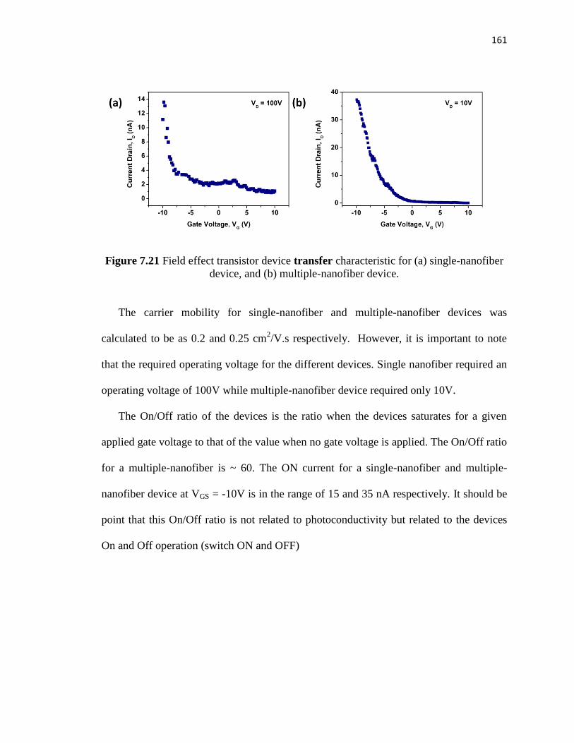
161
Figure 7.21 Field effect transistor device transfer characteristic for (a) single-nanofiber
device, and (b) multiple-nanofiber device.
The carrier mobility for single-nanofiber and multiple-nanofiber devices was
calculated to be as 0.2 and 0.25 cm2/V.s respectively. However, it is important to note
that the required operating voltage for the different devices. Single nanofiber required an
operating voltage of 100V while multiple-nanofiber device required only 10V.
The On/Off ratio of the devices is the ratio when the devices saturates for a given
applied gate voltage to that of the value when no gate voltage is applied. The On/Off ratio
for a multiple-nanofiber is ~ 60. The ON current for a single-nanofiber and multiple-
nanofiber device at VGS = -10V is in the range of 15 and 35 nA respectively. It should be
point that this On/Off ratio is not related to photoconductivity but related to the devices
On and Off operation (switch ON and OFF)

162
To further confirm the field effect transistor (FET) behavior nanofibers, different
values of Vg are applied to control the conductivity in the channel. Figure 7.22 shows
output characteristics of a BFO single-nanofiber and multiple-nanofiber FET device. The
non-linear ID-VD curve with pinch off behavior indicates that the device works as a FET.
Figure 7.22 Field effect transistor device output characteristic for (a) single-nanofiber
device, and (b) multiple-nanofiber device.
In general, the electronic properties of semiconductor nanofibers depend on its
diameter. Nevertheless, the relationship between the nano-dimensions and properties is
very complex, thus required careful experiments and deeper understanding. An
experimental difficulty is that studying the effects of different diameters requires
comparisons of individual nanofibers of one batch of precursor solution. Such
comparison relies on the assumption that the different growth conditions (different
batches) do not affect electronic properties nanofibers.

163
7.6 Summary
Bismuth ferrite nanofibers with excellent surface morphology have been fabricated by
electrospinning technique. Nanofibers with controlled diameter were achieved by varying
the precursor solution concentration. Bead free- nanofibers with diameter in a range of 20
- 110 nm were obtained. XRD, complementary Raman spectroscopy and TEM results
show that BFO nanofibers have pure perovskite phase with rhomobohedral structure. The
grain size decreased sharply for nanofibers below 60 nm in diameter. The nanofibers are
mostly a combination of Fe valence state, thinner nanofiber (20 nm) favored Fe3+
while
thicker nanofibers are most likely Fe2+
.
The electrical properties of BFO nanofibers exhibited a diameter dependent which
could be correlated to the grain size. Larger diameter resulted in higher current levels but
lower electron-hole recombination in the photoconductivity process. BFO single and
multiple nanofiber field effect transistors devices exhibited a p-type semiconductor
behavior. The carrier mobility for both devices is ~ 0.20cm2/V.s. while the operating
voltage for multiple-nanofibers devices is greatly reduced from 100 V to 10 V compared
to single nanofiber device.
One dimensional BFO nanofibers are emerging as promising candidate for
photoconduction and photovoltaic applications due to the strong light absorption which
are result of large surface areas and direct charge transport along the geometry of the
nanofibers.
.

164
7.7 References
1. Baji, A. et al. One-dimensional multiferroic bismuth ferrite fibers obtained by
electrospinning techniques. Nanotechnology 22, 235702 (2011).
2. Li, D. & Xia, Y. Electrospinning of Nanofibers: Reinventing the Wheel? Adv.
Mater. 16, 1151–1170 (2004).
3. Ziabari, M., Mottaghitalab, V. & Haghi, A. K. A new approach for optimization
of electrospun nanofiber formation process. Korean J. Chem. Eng. 27, 340–354 (2010).
4. Doshi, J. & Reneker, D. H. Electrospinning process and applications of
electrospun fibers. J. Electrost. 35, 151–160 (1995).
5. Fong, H. & Reneker, D. H. in Structure formation in polymeric fibers 6, (2001).
6. Tan, S.-H., Inai, R., Kotaki, M. & Ramakrishna, S. Systematic parameter study
for ultra-fine fiber fabrication via electrospinning process. Polymer 46, 6128–6134
(2005).
7. Deitzel, J. M., Kleinmeyer, J., Harris, D. & Beck Tan, N. C. The effect of
processing variables on the morphology of electrospun nanofibers and textiles. Polymer
42, 261–272 (2001).
8. Fukumura, H. et al. Raman scattering study of multiferroic BiFeO3 single crystal.
J. Magn. Magn. Mater. 310, e367–e369 (2007).
9. Palai, R. et al. β phase and γ-β metal-insulator transition in multiferroic BiFeO3.
Phys. Rev. B 77, (2008).
10. Singh, M. K., Jang, H. M., Ryu, S. & Jo, M.-H. Polarized Raman scattering of
multiferroic BiFeO3 epitaxial films with rhombohedral R3c symmetry. Appl. Phys. Lett.
88, 042907 (2006).
11. Da-Ren Chen, D. Y. H. P. Electrospraying of conducting liquids for monodisperse
aerosol generation in the 4 nm to 1.8 μm diameter range. J. Aerosol Sci. 963–977 (1995).
doi:10.1016/0021-8502(95)00027-A
12. Jaiswal, A. et al. Effect of Reduced Particle Size on the Magnetic Properties of
Chemically Synthesized BiFeO3 Nanocrystals. J. Phys. Chem. C 114, 2108–2115 (2010).
13. Tsai, D.-S. Pressure buildup and internal stresses during binder burnout:
Numerical analysis. AIChE J. 37, 547 – 554 (2004).
14. Hou, J. J. et al. Diameter dependence of electron mobility in InGaAs nanowires.
Appl. Phys. Lett. 102, 093112 (2013).
15. Scheffler, M., Nadj-Perge, S., Kouwenhoven, L. P., Borgström, M. T. & Bakkers,
E. P. A. M. Diameter-dependent conductance of InAs nanowires. J. Appl. Phys. 106,
124303 (2009).
16. Calarco, R. et al. Size-dependent Photoconductivity in MBE-Grown
GaN−Nanowires. Nano Lett. 5, 981–984 (2005).
17. Neamen, D. A. Semiconductor Physics And Devices: Basic Principles. (McGraw-
Hill, 2011).
18. Prashanthi, K., Gaikwad, R. & Thundat, T. Surface dominant photoresponse of
multiferroic BiFeO 3 nanowires under sub-bandgap illumination. Nanotechnology 24,
505710 (2013).
19. Alexe, M. & Hesse, D. Tip-enhanced photovoltaic effects in bismuth ferrite. Nat.
Commun. 2, 256 (2011).

165
20. Choi, T., Lee, S., Choi, Y. J., Kiryukhin, V. & Cheong, S.-W. Switchable
ferroelectric diode and photovoltaic effect in BiFeO3. Science 324, 63–66 (2009).
21. MOSFET and Metal Oxide Semiconductor Tutorial. Basic Electronics Tutorials
at <http://www.electronics-tutorials.ws/transistor/tran_6.html>
166
8 Summary and Conclusions
In this thesis, fabrication and ferroelectric properties, leakage current, photoconductor
behavior, and transistor performance of the lead free multiferroic bismuth ferrite-BiFeO3
based thin films and nanofibers were investigated. Thin films were fabricated by sol-gel
solution and pulsed laser deposition (PLD) methods. Nanofibers were fabricated by
electrospinning of sol-gel solutions.
The optimum deposition conditions for BiFe1-xMnxO3 (x=0.00 to 0.15) thin films by
sol-gel are as follow: spin coating at 3000 rpm for 30 seconds, pyrolysis at 200 ◦C for 2
minutes, and heat treatment at 550 ◦C for 10 minutes.
Epitaxial (100) oriented thin films of 0.6BiFeO3-0.4(Bi0.5K0.5)TiO3 were prepared by
PLD under different oxygen background pressure of 300, 400, and 500 mTorr, 10 Hz
laser fluency, 800 ◦C substrate temperature, and 170 mJ laser energy. Under similar
deposition method, bi-layered epitaxial (100) oriented thin films with targets
compositions of 0.88(Bi0.5Na0.5)TiO3 -0.08(Bi0.5K0.5)TiO3-0.04BaTiO3 (BNT-BKT-BT)
and BiFeO3 were deposited on SrRuO3 coated SrTiO3 substrate. In this investigation,
first, BNT-BKT-BT film with thickness of 150 nm, was deposited with following
deposition parameters: substrate temperature 800 °C, oxygen partial pressure 400 mTorr,
laser energy 170 mJ, laser repetition rate10 Hz. In second step, BFO thin film with
thickness of 150 nm was deposited on top of the BNT-BKT-BT layer with following
deposition parameters: substrate temperature of 750 °C, 20 mTorr oxygen pressure, 170
mJ laser energy, and 10 Hz laser repetition.

167
BFO based nanofibers were fabricated by electrospinning technique and nanofibers
morphology, structure, and electrical behavior were studied for possible high power
electronics devices applications. The optimized electrospinning processing conditions for
the deposition of pure BFO nanofibers with an excellent morphology, free of beads,
smooth, and uniform surface are: 0.2 ml/hr flow rate, 10 kV driving voltage, and 20 cm
separation between the needle tip and collector.
Detailed conclusions were drawn from the numerous experiments carried out on BFO
thin films and nanofibers which are presented as follows:
A) Bismuth ferrite thin films by sol gel
BFO-Mn thin films exhibited pure perovskite structure up to 15 mol% Mn doped.
The films structure go through a transition from rhombohedral to tetragonal when
Mn increased above 5%
The surface microstructure for higher Mn content resulted in pillar growth.
The leakage current of 5% Mn doped BFO films two orders of magnitude
suppressed.
168
B) 0.6BiFeO3-0.4(Bi0.5K0.5)TiO3 thin films by pulsed laser deposition
Films deposited at different oxygen partial pressure show a pure perovskite
structure with no impurities.
The films grown under 300 mTorr exhibited a Bi/Fe ratio very close to the target
composition. Surface morphology of the films is dense, uniform and pinhole or
crack free.
The leakage current of the films grown at 300 mTorr was 10-4
A.cm-2
at 200
kV.cm-1
which is suppressed by four orders of magnitudes compared to the films
grown at 500 mTorr oxygen partial pressure.
The optimum electrical and ferroelectric properties are as: Oxygen Pressure 300
mTorr, Pr = 16.6 C.cm-2
, EC = 100 kV.cm-1
, and Jsc = 1 10-4
(A.cm-2
) at 200
kV.cm-1
, and r = 400 at 1 kHz.
C) 0.88(Bi0.5Na0.5)TiO3-0.08(Bi0.5K0.5)TiO3-0.04BaTiO3/BiFeO3 bi-layered thin
films by pulsed laser deposition
The BNT-BKT-BT/BFO bi-layered thin films exhibited a pure perovskite phase.
The surface morphology of the top layer (BFO) shows a pillar type growth.
Films exhibited remnant polarization values of 22.0 C.cm-2
, Ec = 100 kV.cm-1
,
and r = 140 at 1 kHz.
The leakage current of the bi-layered film was 10-3
A.cm-2
, which is three orders
of magnitudes lower than un-doped BFO films.
169
D) Bismuth ferrite nanofibers by electrospinning
The nanofibers diameter was well controlled with the precursor solution
concentration, in a range of 20 to 110 nm.
Iron valence state was found to vary with nanofiber diameter which could be
related to the shell/core ratio or organic polymer removal.
EELS experiments revealed that iron valence state for a 20 nm nanofiber was
mostly 3+ while iron valence state for nanofibers with larger diameter (80 nm or
thinner) was mostly 2+. However, the iron valance sate for nanofibers in a range
of 20-80 nm in diameter are a combination of 3+ and 2
+ which was confirmed by
TEM and XPS.
The I-V increases from 10 to 80 nA for single BFO nanofibers with diameters of
20 and 50 nm respectively.
The photoresponse (I-t) upon illumination, for nanofibers mat was dependent on
the nanofiber average diameter. For samples with nanofibers of ± 20 nm, the
Light On/Light Off ratio was four hundred times higher than of nanofibers with
± 100 nm diameter.
The BFO nanofiber field effect transistor devices exhibited a p-type
semiconductor behavior, and the conduction channel is well controlled. The
device is OFF for VGS > 0V and it is switched ON for VGS < 0V.
The device carrier mobility is found to be as 0.20 to 0.25 cm2/V.s for multiple and
single nanofiber FET respectively. However, the required operating voltage for a
single nanofiber is 100V while for a multiple-nanofiber is 10V.
170
According to the obtained results in this thesis, it can be concluded that lead free
multiferroic bismuth ferrite binary system and bi-layered thin film could be utilized in for
memory applications. Bismuth ferrite as mid band gap semiconductor in the form of
nanofibers is a potential candidate for photoconduction applications and high power
electronic devices.

171
9 Suggestions for Future Work
Bismuth ferrite and its multiferroic properties have been extensively studied in the
form of thin films through many years. However, its multiferroic origin still is not well
understood and more research needs to be done in this area. The development of BFO in
one dimensional structure is at its early stage. Most of the work being done in BFO
nanofibers attempts to enhance the ferromagnetic behavior. It has been found than the
multiferroic properties of BFO are size and structural dependent. The weak spiral spin
structure and antiferromagnetic ordering can be suppressed and high magnetoelectric
coupling may be observed if the size of the nanostructure is less than the spiral
periodicity (62 nm). Considering the ferroelectric-semiconductor multi-functionality of
BFO, novel applications in the field of optoelectronics are being studied recently.
In this section few suggestions are made to conduct research in the area of BFO thin
films and nanofibers as continuation of the presented work.
E) Bismuth ferrite thin films
1. Improve the surface quality of BFO thin films by lowering the deposition
temperature and/or increasing the oxygen partial pressure by PLD. Characterize
the thin films (PLD and sol-gel) electromechanical properties at low temperature
and/or high frequency.
2. Considering that the development of BFO-BKT thin films is not being
extensively studied by others group, further experiments could be revealing.
Deposition of BFO-BKT thin films by PLD at lower oxygen pressure and
investigation of better ferroelectric properties are achievable.

172
F) Bismuth ferrite nanofibers
1. Characterize the multiferroic properties of BFO: single nanofibers, nanofibers
mat, and aligned nanofibers using piezo-atomic force microscopy.
2. The carrier mobility in nanostructures becomes size dependent when the size is
reduced below the excitation Bohr atom radius. Fabrication of nanostructures
below such radius to obtain higher carrier mobility on transistor devices.
3. Investigate the photo-catalytic behavior of nanofibers.
4. Fabrication of BFO based solar cell.
5. Fabrication and characterization of other lead free piezoelectric materials such
as BNT, BKT, BT and combination of them.


