
Curiosity Bits Python Tutorial: Mining Facebook Fan Page - getting posts and comments
���������� TUTORIAL
ARCHIVE 2007
TUTORIAL 2 “AN OVERVIEW OF CRITICAL ISSUES IN IC
PACKAGING” by
Charles Cohn – Senior Analyst, TechSearch International
SEMICONDUCTOR PACKAGING has become increasingly critical as the package becomes the limiting factor in integrated circuit (IC) performance. This tutorial provides insight into the important aspects of these critical packaging issues. Topics include an overview of the IC packages used in volume production, trends in IC packages such as body size, pin count, and package pitch. Materials and test issues will also be addressed.
COPYRIGHT NOTICE
The papers in this publication comprise the proceedings of the 2007 BiTS Workshop. They reflect the authors’ opinions and are reproduced as presented , without change. Their inclusion in this publication does not constitute an endorsement by the BiTS Workshop, the sponsors, BiTS Workshop LLC, or the
authors.
There is NO copyright protection claimed by this publication or the authors. However, each presentation is the work of the authors and their respective companies: as such, it is strongly suggested that any use
reflect proper acknowledgement to the appropriate source. Any questions regarding the use of any materials presented should be directed to the author/s or their companies.
All photographs in this archive are copyrighted by BiTS Workshop LLC. The BiTS logo and ‘Burn-in & Test Socket Workshop’ are trademarks of BiTS Workshop LLC.
20072007Tutorial 2
March 11 - 14, 2007 1
BITS3.07 © 2007 TechSearch International, Inc. 1
Charles CohnSenior Analyst
March 11, 2007
Charles CohnSenior Analyst
March 11, 2007
TechSearch International, Inc.www.techsearchinc.com
20072007Tutorial 2
March 11 - 14, 2007 2
BITS3.07 © 2007 TechSearch International, Inc. 2

20072007Tutorial 2
March 11 - 14, 2007 3
BITS3.07 © 2007 TechSearch International, Inc. 3
• Packaging of ICs is no longer the mundane process that took place at the end of the chip supply chain. For most products, today’s packaging requires high level coordination between silicon and package designers.
• The proliferation of package technologies can be attributed to technical (performance) and cost demands being placed on the package by the device and system engineers.
• The high performance, increased functionality and space-sensitive applications have resulted in an increased rate of advanced IC package solutions to satisfy the demand.
• As a result of the extreme cost pressure that has been exerted on the electronic industry, package solutions that offer the minimum level of performance at the lowest cost will continue to be in demand.

20072007Tutorial 2
March 11 - 14, 2007 4
BITS3.07 © 2007 TechSearch International, Inc. 4
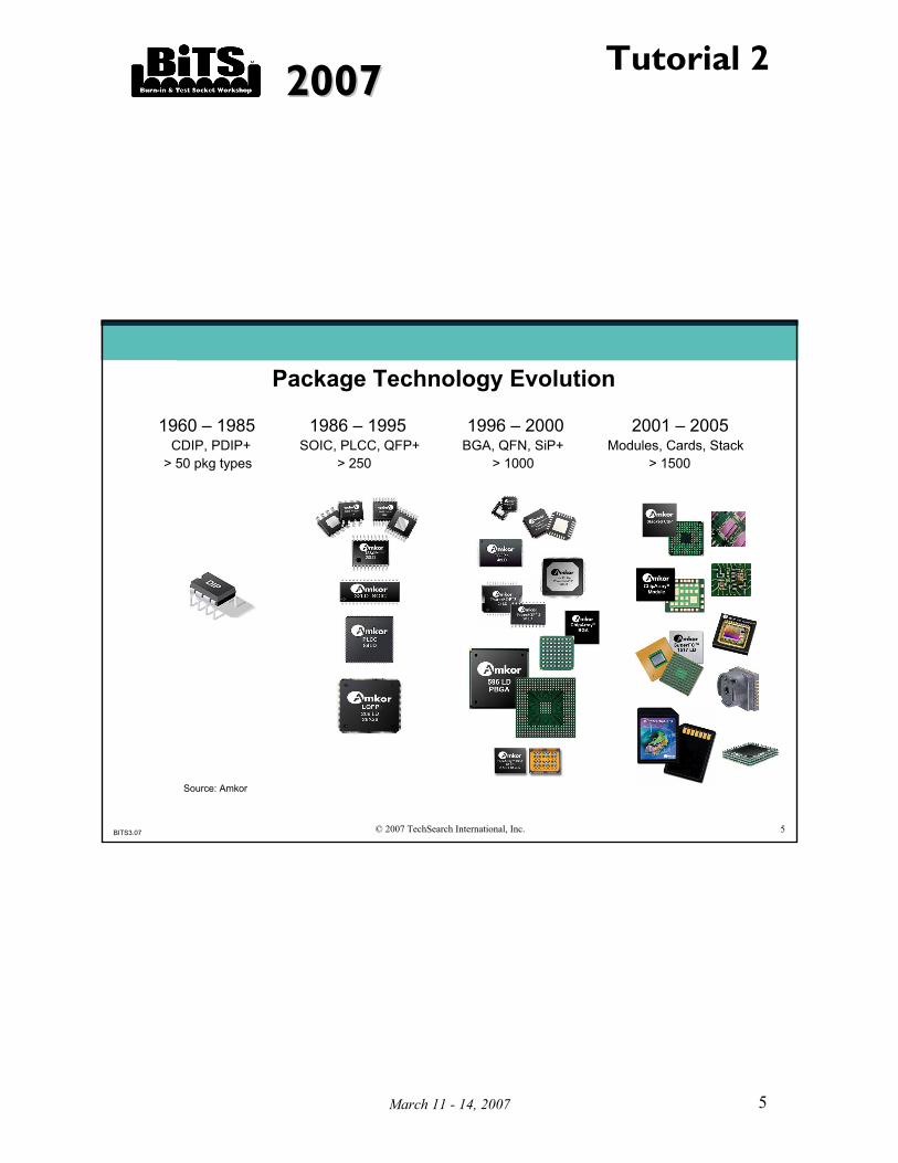
Package Technology Evolution
PoP
SiP
20072007Tutorial 2
March 11 - 14, 2007 5
BITS3.07 © 2007 TechSearch International, Inc. 5
1960 – 1985CDIP, PDIP+
> 50 pkg types
1986 – 1995SOIC, PLCC, QFP+
> 250
1996 – 2000BGA, QFN, SiP+
> 1000
2001 – 2005Modules, Cards, Stack
> 1500
Package Technology Evolution
Source: Amkor
20072007Tutorial 2
March 11 - 14, 2007 6
BITS3.07 © 2007 TechSearch International, Inc. 6
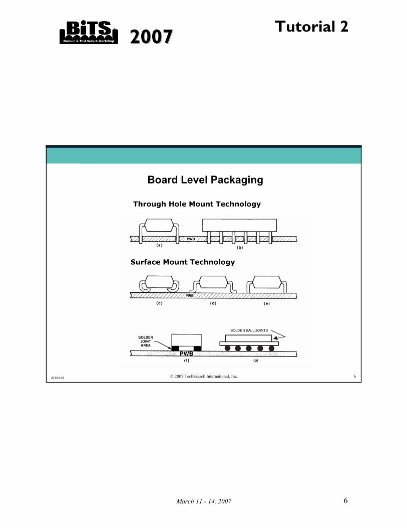
Board Level Packaging
Through Hole Mount Technology
Surface Mount Technology

20072007Tutorial 2
March 11 - 14, 2007 7
BITS3.07 © 2007 TechSearch International, Inc. 7
Prefabricated Metallized Ceramic Packages

20072007Tutorial 2
March 11 - 14, 2007 8
BITS3.07 © 2007 TechSearch International, Inc. 8
Prefabricated Ceramic/Plastic Packaging

20072007Tutorial 2
March 11 - 14, 2007 9
BITS3.07 © 2007 TechSearch International, Inc. 9
Postmolded Plastic Packaging

20072007Tutorial 2
March 11 - 14, 2007 10
BITS3.07 © 2007 TechSearch International, Inc. 10
Postmolded Plastic Packaging

20072007Tutorial 2
March 11 - 14, 2007 11
BITS3.07 © 2007 TechSearch International, Inc. 11
Typical QFP in a Postmolded Plastic Technology

20072007Tutorial 2
March 11 - 14, 2007 12
BITS3.07 © 2007 TechSearch International, Inc. 12
Driving Forces in Package Selection
• Product Application• Silicon Technology• Operating Frequencies• No. of Input/Output Requirements• Power Dissipation• Environmental Operating Conditions• Package Size• Board Packaging Density• Board Level Packaging Technology (Surface Mount/Through-
Hole Mount)• Compatibility with Existing Handling Equipment• Time to Market• Cost Cost Cost Cost

20072007Tutorial 2
March 11 - 14, 2007 13
BITS3.07 © 2007 TechSearch International, Inc. 13
Next Generation IC Package Requirements
Smaller Package
Reduced Signal Line Length
Low Thermal Resistivity
Matched TCE Materials
Low Resist. Conductor Metal
Low Dielectric Constant, Dk & Low Dissipation Factor, Df Materials
Lower Cross Talk Noise Design
Low Inductance
Matched Diff. Impedances
High Density
High Performance Package
High Thermal Dissipation
Improved Signal Transmission

20072007Tutorial 2
March 11 - 14, 2007 14
BITS3.07 © 2007 TechSearch International, Inc. 14
Future Trends in IC Packages
• I/O count to increase• Lead/ball pitches will decrease• Packages will get thinner and lighter• IC pad pitches will get smaller• Area array pkgs. will grow in demand• Higher performance, multilayer packages will be in demand• Stacked die or modules such as system-in-package (SiP)• Demand for ICs without packages will grow• Package costs will decline• Faster time to market requirements
20072007Tutorial 2
March 11 - 14, 2007 15
BITS3.07 © 2007 TechSearch International, Inc. 15
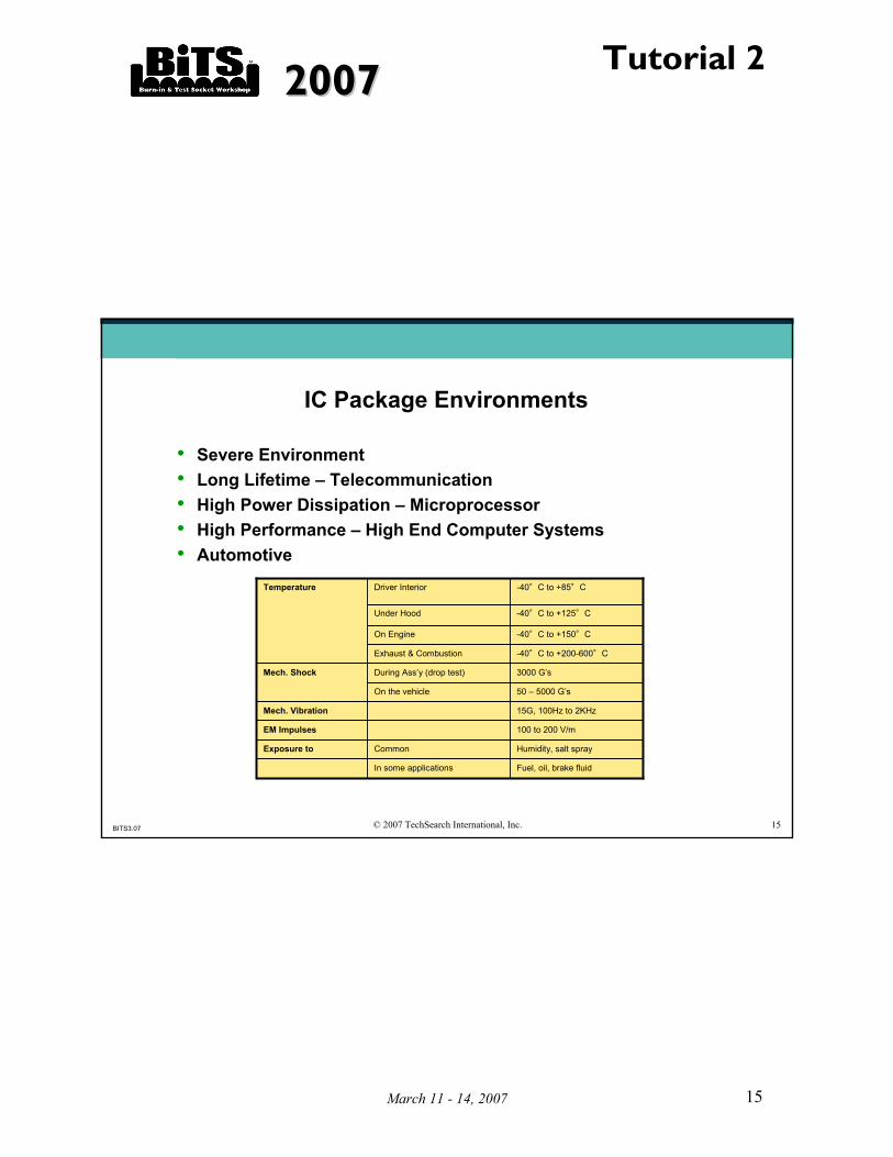
IC Package Environments
• Severe Environment• Long Lifetime – Telecommunication• High Power Dissipation – Microprocessor• High Performance – High End Computer Systems• Automotive
Fuel, oil, brake fluidIn some applications
Humidity, salt sprayCommonExposure to
100 to 200 V/mEM Impulses
15G, 100Hz to 2KHzMech. Vibration
50 – 5000 G’sOn the vehicle
3000 G’sDuring Ass’y (drop test)Mech. Shock
-40°C to +200-600°CExhaust & Combustion
-40°C to +150°COn Engine
Temperature
-40°C to +125°CUnder Hood
-40°C to +85°CDriver Interior

20072007Tutorial 2
March 11 - 14, 2007 16
BITS3.07 © 2007 TechSearch International, Inc. 16
PBGA Qualification Tests for High Performance
PACKAGE ASSEMBLY
PACKAGE ASSEMBLY
DIE SHEAR STRENGTH MIL-STD-883D, MTD 2019DIE SHEAR STRENGTH MIL-STD-883D, MTD 2019
PHYSICAL DIMENSIONSMIL-STD-883D, MTD 2016
PHYSICAL DIMENSIONSMIL-STD-883D, MTD 2016
WIRE BOND STRENGTHMIL-STD-883D, MTD 2011, Cond D
WIRE BOND STRENGTHMIL-STD-883D, MTD 2011, Cond D
BURN-IN TEST125ºC, 24 hrs. Over Bias
(depending on application)
BURN-IN TEST125ºC, 24 hrs. Over Bias
(depending on application)
ELEC. TEST
ESD (HBM & CDM)MIL-STD-883D, MTD 3015.7
ESD (HBM & CDM)MIL-STD-883D, MTD 3015.7
LATCH UP (LU)JEDEC STD # 17
LATCH UP (LU)JEDEC STD # 17
FLAMMABILITYUL 94-V-0, O2. INDEX 28% MIN
FLAMMABILITYUL 94-V-0, O2. INDEX 28% MIN
SOLVENT RESIST.MIL-STD-883D, MTD 2015
(ink only)
SOLVENT RESIST.MIL-STD-883D, MTD 2015
(ink only)
SOLDER BALL INTEGRITY
SOLDER BALL INTEGRITY
ELEC. TEST
HIGH TEMP. OPER. BIAS (HTOB)
MIL-STD-883, MTD 1005Ta=125ºC, Tj<150ºC,
Over Bias Volt., 1000 hrs
HIGH TEMP. OPER. BIAS (HTOB)
MIL-STD-883, MTD 1005Ta=125ºC, Tj<150ºC,
Over Bias Volt., 1000 hrs
MOISTURE PRECONDITIONING
3 Reflows (JEDEC Level 2A)
MOISTURE PRECONDITIONING
3 Reflows (JEDEC Level 2A)
COMPONENT LEAD ASS’YSIMULATION SEQUENCE (CLASS)
FLUX, 3 Reflows, CLEAN,(Target JEDEC Level 2A)
COMPONENT LEAD ASS’YSIMULATION SEQUENCE (CLASS)
FLUX, 3 Reflows, CLEAN,(Target JEDEC Level 2A)
VISUAL INSP.
ELEC. TEST
ELEC. TEST
TEMP. HUM.BIAS (THB)
85ºC, 85% RH, Biased, 1000 hrs
.
TEMP. HUM.BIAS (THB)
85ºC, 85% RH, Biased, 1000 hrs
.
(Alternate to THB) HAST
130ºC, 85% RH, Biased, 96 hrs.
(Alternate to THB) HAST
130ºC, 85% RH, Biased, 96 hrs.
VISUAL INSPEC.ELEC. TEST
TEMP. CYCLING (TC)MIL-STD-883D, MTD 1010,
Cond B, -55 to +125ºC, 1K Cy
TEMP. CYCLING (TC)MIL-STD-883D, MTD 1010,
Cond B, -55 to +125ºC, 1K Cy
ELEC. + CSAM
VISUAL INSPEC.ELEC. TEST
ELEC. TEST
Unbiased HAST130ºC, 85% RH,
96 / 168 hrs.
Unbiased HAST130ºC, 85% RH,
96 / 168 hrs.
(Alt. to HAST)STEAM BOMB
121ºC, 100% RH, 2 Atm 168 hrs (u/b)
(Alt. to HAST)STEAM BOMB
121ºC, 100% RH, 2 Atm 168 hrs (u/b)
ELEC. TEST
CSAM TEST
ELEC. TEST
CSAM TEST
VISUAL INSP. ELEC. TEST
20072007Tutorial 2
March 11 - 14, 2007 17
BITS3.07 © 2007 TechSearch International, Inc. 17
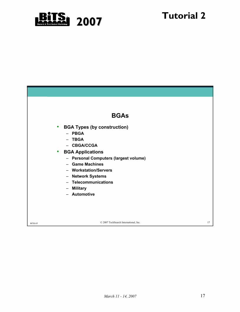
BGAs
• BGA Types (by construction)– PBGA– TBGA– CBGA/CCGA
• BGA Applications– Personal Computers (largest volume)– Game Machines– Workstation/Servers– Network Systems– Telecommunications– Military– Automotive

20072007Tutorial 2
March 11 - 14, 2007 18
BITS3.07 © 2007 TechSearch International, Inc. 18
BT/Glass PCB
Silica-FilledEpoxy Overmold
(or Glob-Top)
Routing Vias
62Sn/36Pb/2Ag or 63Sn/37Pb or Pb-free (SAC alloy - 95.5Sn/4.0Ag/0.5Cu)
Solder Ball
Silicon DieAg-Filled Die AttachAu Bond Wires
1.0, 1.27 or 1.50 mm Pitch
0.36, 0.56 or0.60 mm
0.80, 0.90or 1.17 mm
FR-4/Glass PCB Solder Pads
Stand-Off(Variable)
PBGA Construction
Thermal andGround Vias
20072007Tutorial 2
March 11 - 14, 2007 19
BITS3.07 © 2007 TechSearch International, Inc. 19
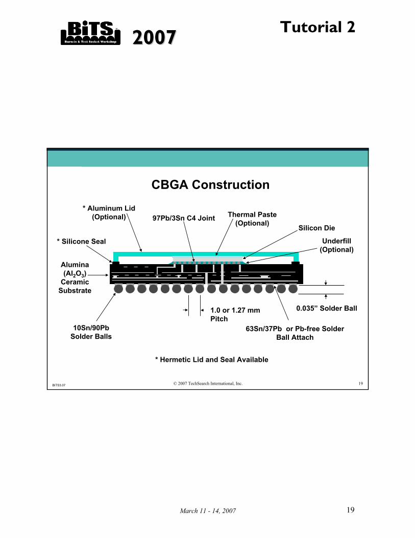
CBGA Construction
Thermal Paste(Optional) Silicon Die
* Aluminum Lid(Optional)
Underfill(Optional)
* Silicone Seal
* Hermetic Lid and Seal Available
Alumina(Al2O3)
CeramicSubstrate
10Sn/90PbSolder Balls
63Sn/37Pb or Pb-free SolderBall Attach
97Pb/3Sn C4 Joint
0.035” Solder Ball1.0 or 1.27 mm Pitch
20072007Tutorial 2
March 11 - 14, 2007 20
BITS3.07 © 2007 TechSearch International, Inc. 20
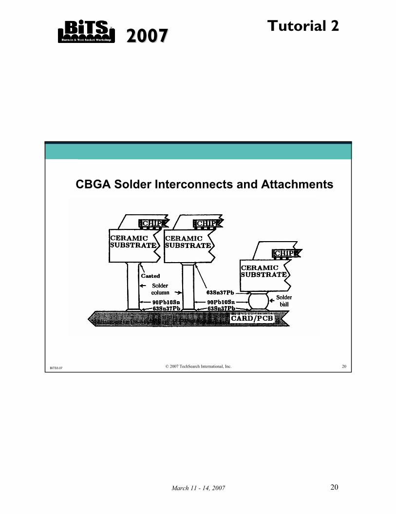
CBGA Solder Interconnects and Attachments

20072007Tutorial 2
March 11 - 14, 2007 21
BITS3.07 © 2007 TechSearch International, Inc. 21
CBGA ConstructionTypical Ceramic Ball Grid Array
(624 Pin, 32 mm Body, 1.27 mm Pitch, 25x25 Array Shown)

20072007Tutorial 2
March 11 - 14, 2007 22
BITS3.07 © 2007 TechSearch International, Inc. 22
IBM’s High Pin Count CCGA

20072007Tutorial 2
March 11 - 14, 2007 23
BITS3.07 © 2007 TechSearch International, Inc. 23
IBM's 2,577 CCGA with 1.0mm pitch
20072007Tutorial 2
March 11 - 14, 2007 24
BITS3.07 © 2007 TechSearch International, Inc. 24
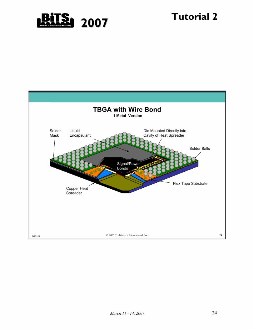
SolderMask
LiquidEncapsulant
Signal/PowerBonds
Die Mounted Directly intoCavity of Heat Spreader
Solder Balls
Copper HeatSpreader
Flex Tape Substrate
TBGA with Wire Bond1 Metal Version

20072007Tutorial 2
March 11 - 14, 2007 25
BITS3.07 © 2007 TechSearch International, Inc. 25
PC High Performance Packaging Trends
• PCs represent increased performance, lower prices• Personal computers were volume driver for IC packages in 1990s,
still driver for BGAs– Ball grid arrays (i.e., chip sets)– Flip chip (all CPUs for PCs now flip chip)– Movement from ceramic to laminate technology
• Major thermal issues for high-performance CPU packaging– TIM1 materials currently include indium solder– Critical need for development of improved thermal interface materials
(TIM)• Integrated circuit I/O counts continue to grow

20072007Tutorial 2
March 11 - 14, 2007 26
BITS3.07 © 2007 TechSearch International, Inc. 26
Workstation/Servers, Network Systems, Telecom
• Sun Microsystems– Highest pin count flip chip packages (728, 784, 1,012, 1,089, 1,155,
1,280, 1,677, 1,848 balls)– 1,848-ball package with 42.5mm x 42.5mm body and 1.0mm ball pitch
in production– SPARC processors still packaged in a ceramic LGA
• Cisco Systems– Ceramic CCGAs up to 1,657 I/O CCGA with flip chip inside– Increasing use of laminate substrate (2,577-ball HyperBGA with a
52.5mm x 52.5mm body size in production)• Motorola Network Processor
– Packaged in a 480-ball TBGA with 37.5x37.5mm body size, 1.27mm ball pitch

20072007Tutorial 2
March 11 - 14, 2007 27
BITS3.07 © 2007 TechSearch International, Inc. 27
PowerPC for Military Applications from White Electronic Design
FC on Board

20072007Tutorial 2
March 11 - 14, 2007 28
BITS3.07 © 2007 TechSearch International, Inc. 28
What’s a CSP
• Chip Scale Package or Chip Size Package?
• Chip size – packages that have the same area as the chip
• Chip scale package is defined as:
• EIAJ/JEDEC defines CSP as a package with an edge dimension no more than 1.2 times that of the die inside
2.1 ≤
AreaDieAreaPackage
EIAJ = Electronics Industries Alliance Japan
JEDEC = Joint Electron Device Engineering Council

20072007Tutorial 2
March 11 - 14, 2007 29
BITS3.07 © 2007 TechSearch International, Inc. 29
0.70 mm
0.36 mm
CSP
Die
Molding Compound Die Attach Epoxy
VTCSP
0.45 mm
0.21 mm
Rigid BT Substrate
Solder Ball
1.36 mm (0.80 mm pitch)
0.88 mm (0.50 mm pitch)
Typical Cross Section of a Plastic CSP Pkg.
20072007Tutorial 2
March 11 - 14, 2007 30
BITS3.07 © 2007 TechSearch International, Inc. 30
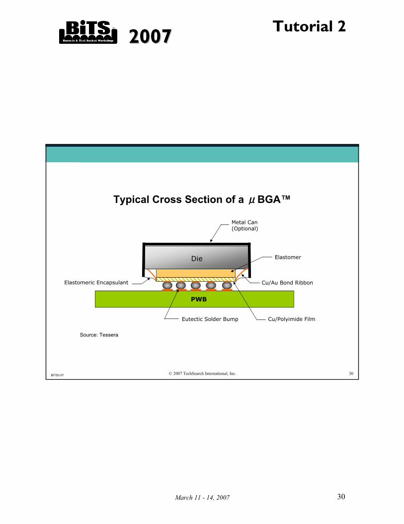
Die
Metal Can (Optional)
Cu/Au Bond Ribbon
Eutectic Solder Bump Cu/Polyimide Film
PWB
Elastomer
Elastomeric Encapsulant
Typical Cross Section of a μBGA™
Source: Tessera

20072007Tutorial 2
March 11 - 14, 2007 31
BITS3.07 © 2007 TechSearch International, Inc. 31
CSPs Worldwide
Source: TechSearch International, Inc.
20072007Tutorial 2
March 11 - 14, 2007 32
BITS3.07 © 2007 TechSearch International, Inc. 32
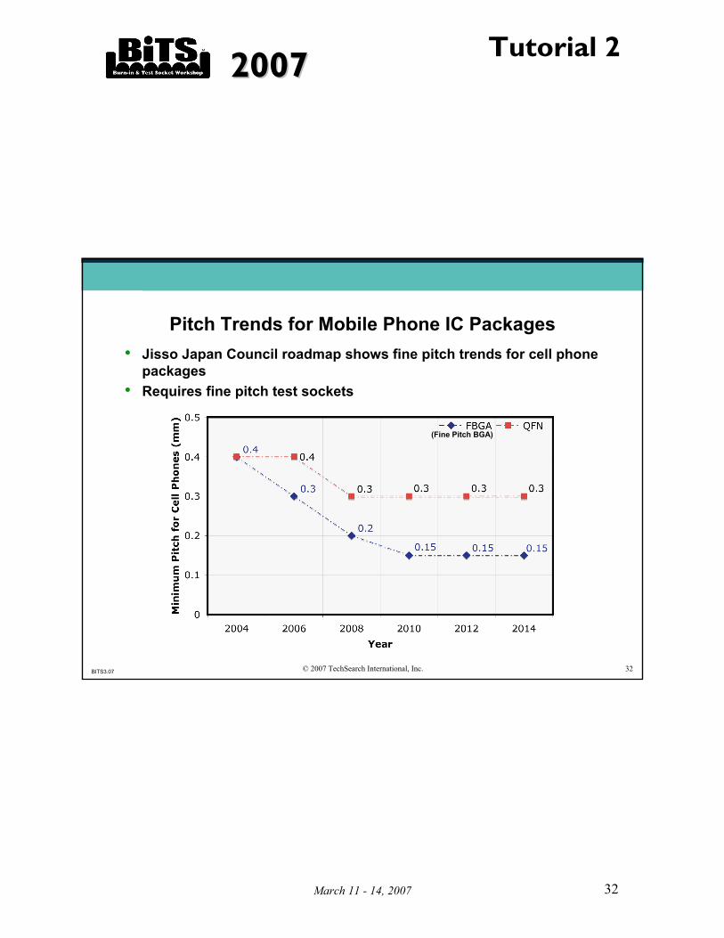
Pitch Trends for Mobile Phone IC Packages• Jisso Japan Council roadmap shows fine pitch trends for cell phone
packages• Requires fine pitch test sockets
(Fine Pitch BGA)

20072007Tutorial 2
March 11 - 14, 2007 33
BITS3.07 © 2007 TechSearch International, Inc. 33
Green Packaging Adoption RatesAlmost all mobile phones have IC packages with lead free solder balls
50%–75%15%–40%Halogen-free Laminate Substrates
30%–60%5%–40%Halogen-free Mold Compound
50%–80%20%–50%Pb-free
Percent of Units Forecasted in 2006
Estimated Percent of Units Shipped
in 2005
“Green” Packaging Technology
Estimated Adoption Rates by Packaging Subcontractors
Source: SEMI and TechSearch International, 2005 Global Semiconductor Packaging Materials Outlook (January 2006)
20072007Tutorial 2
March 11 - 14, 2007 34
BITS3.07 © 2007 TechSearch International, Inc. 34
Driver for CSP Growth
• Mobile phones as volume driver – More than a billion handsets expected to ship in 2007– Mobile phones contain an average 15 CSPs, including wafer level
packages, stacked die packages, and SiP– Mobile phones drive volumes for stacked die packages and system-in-
package (SiP)
• Wafer level packaging demand driven by memory, IPDs, analog devices, power devices, and others
– Applications range from diodes to DRAMs– Mobile phones main application– Potential for DRAM package in mobile phones

20072007Tutorial 2
March 11 - 14, 2007 35
BITS3.07 © 2007 TechSearch International, Inc. 35
Trends in Mobile Phones: Increased Integration• New features are being incorporated in the phone
– WLAN– Bluetooth– FM Radio– MP3 Player– Camera
• Driven by market forces– Technology convergence– New form factors– Smaller, thinner, lighter– Cheaper– Reduced time to market– Environmental
• Challenges– Cost– Density– Reliability– Technology selection– Co-design

20072007Tutorial 2
March 11 - 14, 2007 36
BITS3.07 © 2007 TechSearch International, Inc. 36
High Volume Production of CSPs
• Lead frame-based packages:Bumped Chip Carrier (BCCTM), MicroLeadframe MLF®, MLP, QFNs, and
Small Outline Non-lead Pkgs. (SONs)
• Flex-based packages:µBGA® from Tessera’s licensees, TI’s µStar BGA™ and other wire bond
on tape packages
• Laminate-based packages:ChipArrayTM(CABGA), Intel’s Very Thin Profile Fine Pitch BGA (VFBGA)
and Easy BGA, and other wire bond on laminates• Stacked CSPs, Package-on-package (PoP), Package-in-package (PiP)
20072007Tutorial 2
March 11 - 14, 2007 37
BITS3.07 © 2007 TechSearch International, Inc. 37
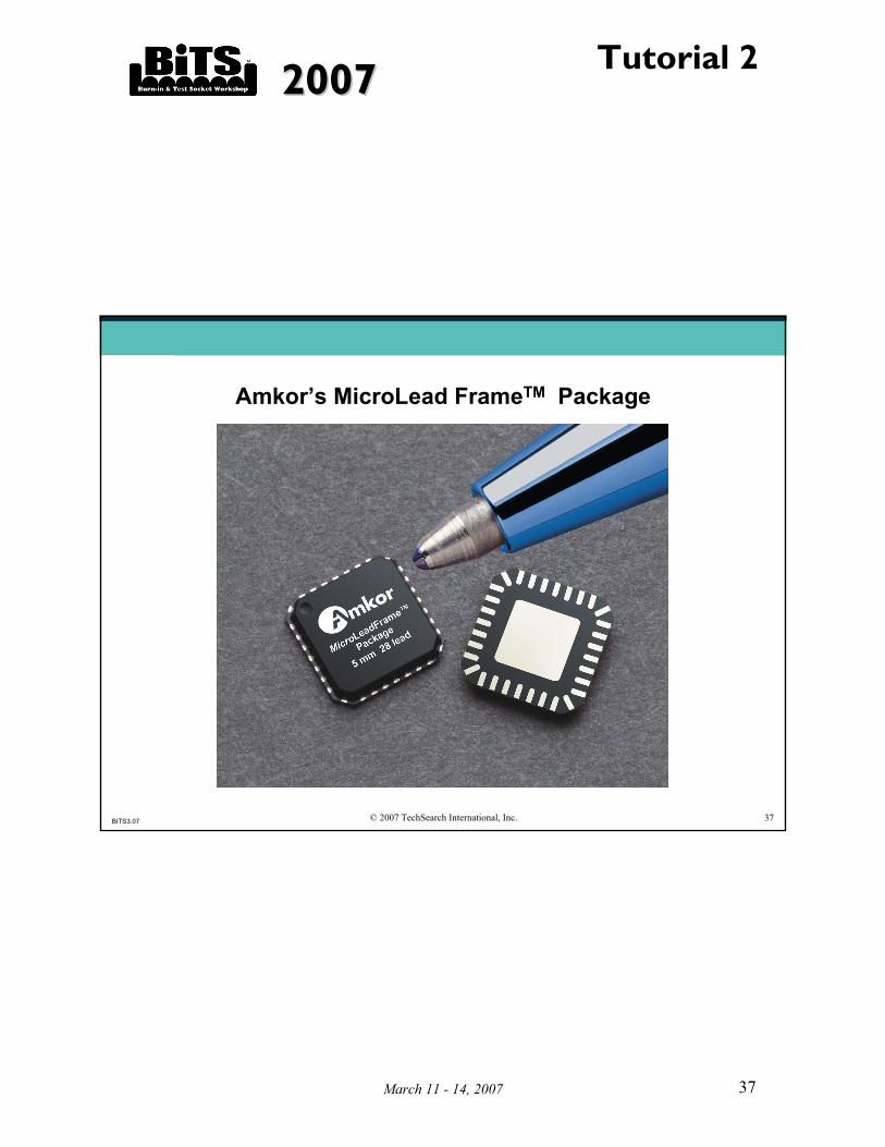
Amkor’s MicroLead FrameTM Package

20072007Tutorial 2
March 11 - 14, 2007 38
BITS3.07 © 2007 TechSearch International, Inc. 38
Amkor’s MicroLead FrameTM Package Cross-section

20072007Tutorial 2
March 11 - 14, 2007 39
BITS3.07 © 2007 TechSearch International, Inc. 39
Fujitsu’s Bump Chip Carrier (BCC++) Process Flow
Source: Fujitsu Microelectronics
Used for RF devices in wireless applications

20072007Tutorial 2
March 11 - 14, 2007 40
BITS3.07 © 2007 TechSearch International, Inc. 40
MicroStar BGA™ Package Structure
0.5mm dia / 0.8mm BALL PITCH Sn/Pb : near eutectic FLEX SUBSTRATE (POLYIMIDE,
TOPSIDE Cu ONLY)
Cu PATTERN
VIA
DIE PASTE
WIRE BONDENCAPSULANT
CHIP
CUSTOMER PWB
20072007Tutorial 2
March 11 - 14, 2007 41
BITS3.07 © 2007 TechSearch International, Inc. 41
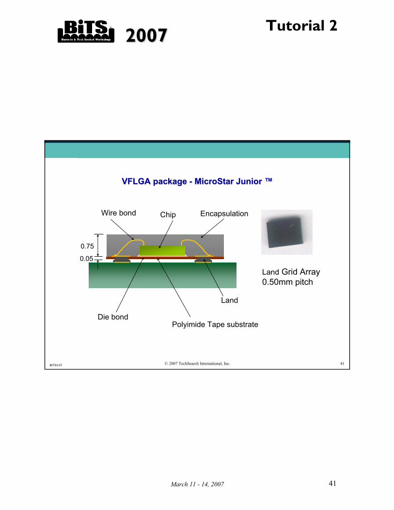
VFLGA package VFLGA package -- MicroStarMicroStar Junior Junior ™™
Land Grid Array0.50mm pitch
Wire bond Chip Encapsulation
Die bondPolyimide Tape substrate
Land
0.05
0.75

20072007Tutorial 2
March 11 - 14, 2007 42
BITS3.07 © 2007 TechSearch International, Inc. 42
Sharp’s Dual Stage Wire Bonding
Source: Sharp.

20072007Tutorial 2
March 11 - 14, 2007 43
BITS3.07 © 2007 TechSearch International, Inc. 43
Sharp Development History and Packaging Roadmap
Source: Sharp.

20072007Tutorial 2
March 11 - 14, 2007 44
BITS3.07 © 2007 TechSearch International, Inc. 44
Intel’s Four-die Stacked Package
Source: Intel
20072007Tutorial 2
March 11 - 14, 2007 45
BITS3.07 © 2007 TechSearch International, Inc. 45
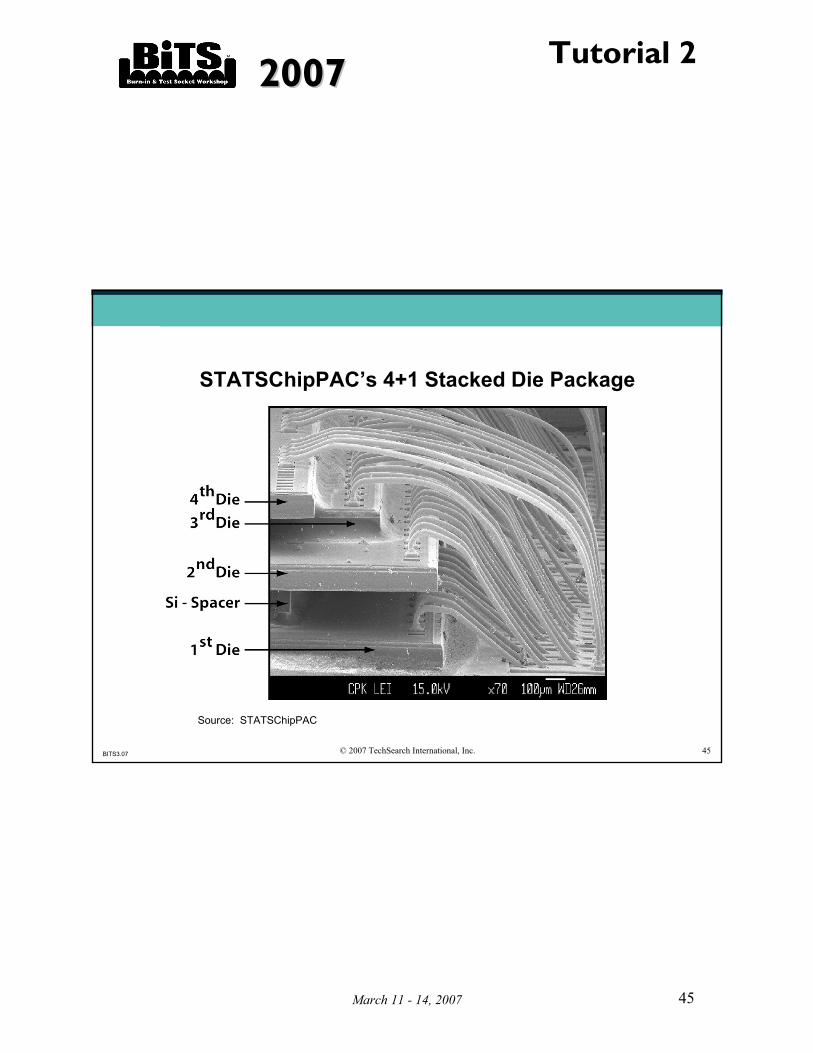
STATSChipPAC’s 4+1 Stacked Die Package
Source: STATSChipPAC

20072007Tutorial 2
March 11 - 14, 2007 46
BITS3.07 © 2007 TechSearch International, Inc. 46
Camera Module & LCD Board FOMA N900i
FBGA(L) 111pin10x11x1.4tP=0.80Substrate 0.15t2 layer
ROHMQFN20pin4.2x4.2x0.8t
FBGA(L) 277pin10x10x1.0tP=0.50Substrate 0.30t4layer(1+2+1)
SON 8pin3x3x1.0tP=0.65 0.250
0.030
0.250
4 chips stacked(3chips+1spacer)
Source: TPSS (A Japan teardown Co.)

20072007Tutorial 2
March 11 - 14, 2007 47
BITS3.07 © 2007 TechSearch International, Inc. 47
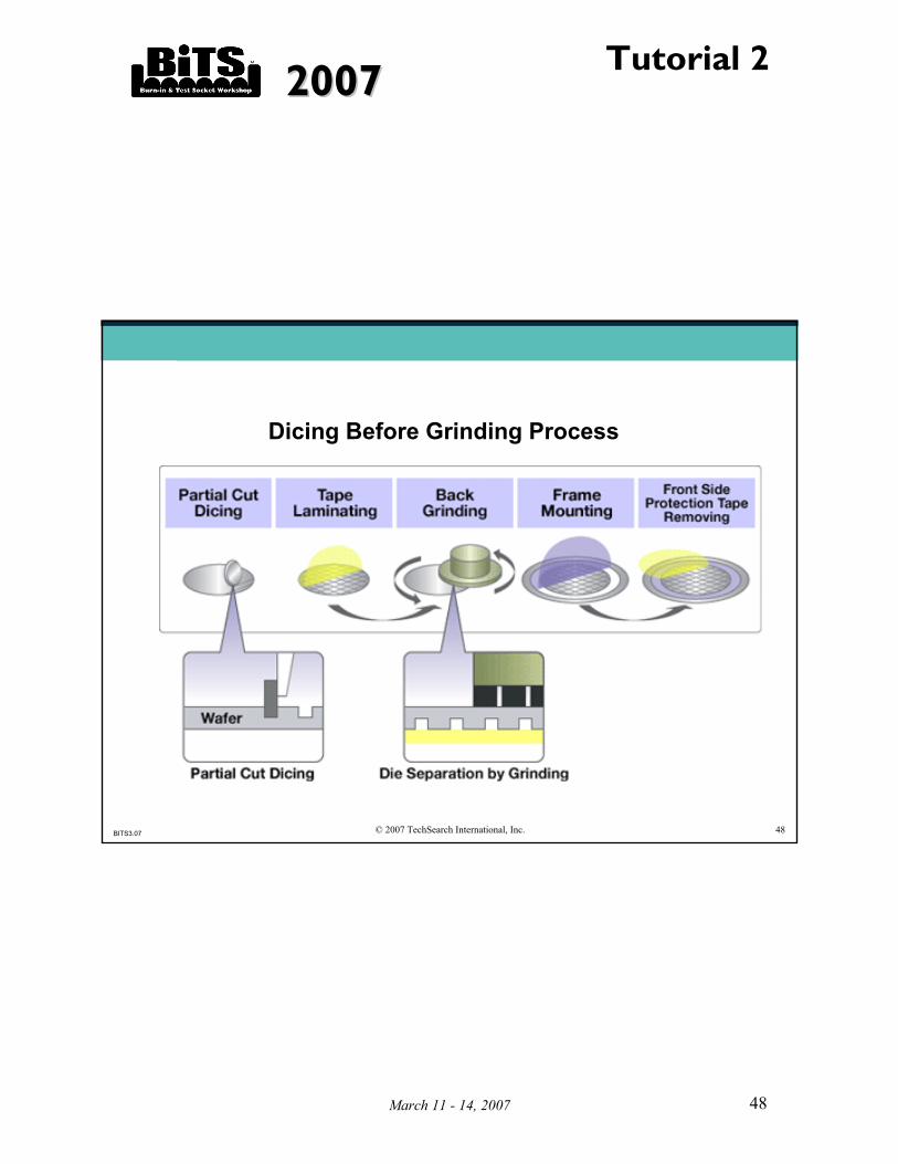
Wafer Thinning Issues for Stacked Die
• Typical wafer thinned by mechanical back grinding– Thickness of 75 µm in production today– New methods for wafer thinning in development– Development work with thickness of 50 to 25 µm
• Flip chip die must be thicker than wire bond die• Most wafers are 200 mm, some 300 mm in diameter• New developments in wafer tape• Challenges in dicing are mechanical, including:
– Handling– Chipping– Flaking
20072007Tutorial 2
March 11 - 14, 2007 48
BITS3.07 © 2007 TechSearch International, Inc. 48
Dicing Before Grinding Process

20072007Tutorial 2
March 11 - 14, 2007 49
BITS3.07 © 2007 TechSearch International, Inc. 49
New Dicing Technology• Laser cutting
– Synova (water jet guided laser)– XSiL– Disco– Shibuya Kogyo– ALSI– ESI– EO Technics– NewWave– Panasonic– Singulase
• Laser scribing followed by dicing blade (for low-K silicon technology)– Advanced Dicing Technologies (ADT)– Disco
• Laser control break– Hamamatsu Photonics
• Plasma– Panasonic
20072007Tutorial 2
March 11 - 14, 2007 50
BITS3.07 © 2007 TechSearch International, Inc. 50
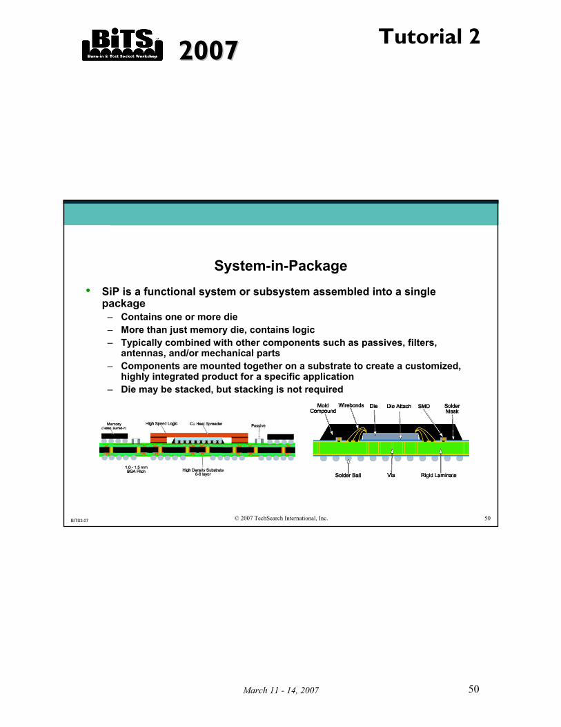
System-in-Package• SiP is a functional system or subsystem assembled into a single
package– Contains one or more die– More than just memory die, contains logic– Typically combined with other components such as passives, filters,
antennas, and/or mechanical parts– Components are mounted together on a substrate to create a customized,
highly integrated product for a specific application– Die may be stacked, but stacking is not required
20072007Tutorial 2
March 11 - 14, 2007 51
BITS3.07 © 2007 TechSearch International, Inc. 51
System-in-Package• SiPs may utilize a combination of advanced packaging including
– Bare die (wire bond or flip chip)– Wafer level packages– Pre-packaged die such as CSP– Stacked packages– Stacked die
• Drivers for SiP– Greater functionality in a smaller area is the driver for consumer and
portable products – High performance is the main driver for computers, telecommunications,
and military/aerospace– Some applications such as medical driven by both– Applications, such as network systems, driven by the need to decrease
motherboard layer counts and complexity• Examples of SiP
– Mobile phones– Consumer product such as camcorders and cameras– Military– High performance SiP applications such as computers and network
systems
20072007Tutorial 2
March 11 - 14, 2007 52
BITS3.07 © 2007 TechSearch International, Inc. 52
System-in-Package Applications
• Mobile phones• MP3 players• Digital still cameras• Digital camcorders• Personal digital assistants• Laptop computers• Mid-range consumer products• Automotive electronics• Medical electronics• Industrial applications• Defense electronics

20072007Tutorial 2
March 11 - 14, 2007 53
BITS3.07 © 2007 TechSearch International, Inc. 53
Why SiPs? According to Renesas (A Mitsubishi/Hitachi Co.) Customer Survey
Source: Renesas Technology
20072007Tutorial 2
March 11 - 14, 2007 54
BITS3.07 © 2007 TechSearch International, Inc. 54
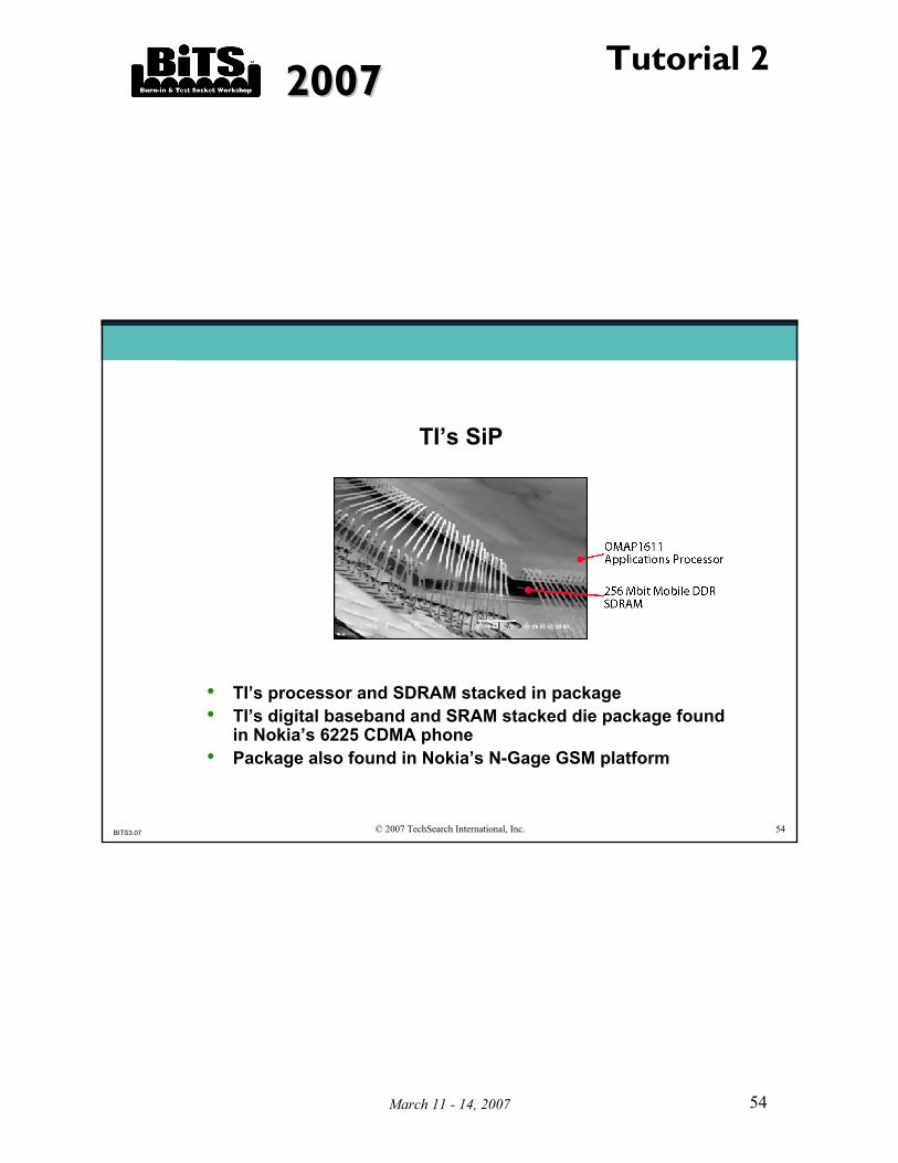
TI’s SiP
• TI’s processor and SDRAM stacked in package• TI’s digital baseband and SRAM stacked die package found
in Nokia’s 6225 CDMA phone• Package also found in Nokia’s N-Gage GSM platform

20072007Tutorial 2
March 11 - 14, 2007 55
BITS3.07 © 2007 TechSearch International, Inc. 55
Package-on-Package (PoP)• Individual packages are stacked on top of each other
– Separate package for logic– Separate package for memory
• At least 10 major OEMs in handset and digital still camera market adopting PoP
• Infrastructure developments were required– Standardization of pin-out footprints for the top stacked package– Required development of package stacking equipment (now 5
equipment suppliers offer PoP mounter)– IC package subcontractor (some early examples)– Board level assembly service provider does
stacking of packages (most cases) and 5 major EMS providers in production or development

20072007Tutorial 2
March 11 - 14, 2007 56
BITS3.07 © 2007 TechSearch International, Inc. 56
Concerns• Slightly larger / thicker Package stack• Co-design for bottom and top packages• Infrastructure for package stacking
Concerns• KGD required for high product yield• Single-sourced product• New development needed to change a device or handle die shrink• Compound yield and multi test
Prospects• OEM (Original Equipment Mfg.) ownership• Flexible memory sources, facilitate memory capacity increases • Tested at individual package level for Known Good Device
Prospects• IDM (Independent Device Mfg.) ownership • Smaller body size and lower package profile
PoPStacked Die
Stacked Die vs. PoP – Trade-offs
Source: Amkor

20072007Tutorial 2
March 11 - 14, 2007 57
BITS3.07 © 2007 TechSearch International, Inc. 57
Now
Thinner substrate
Thinner molding
Lower ball height
1.2mm (cavity substrate for both packages)
1.4mm (cavity substrate for either package)
1.6mm (no cavity substrate)
PoP Board Mounting Height
Source: Amkor
20072007Tutorial 2
March 11 - 14, 2007 58
BITS3.07 © 2007 TechSearch International, Inc. 58
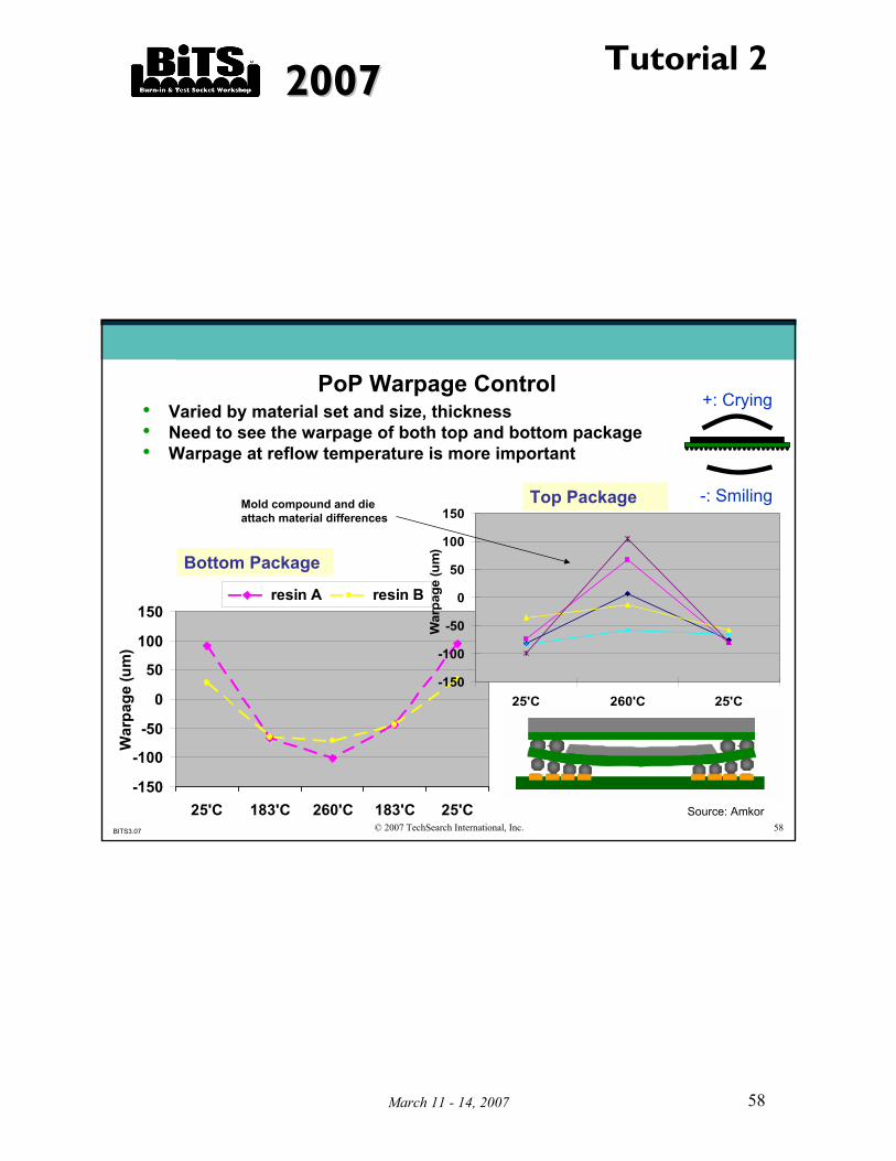
PoP Warpage Control
-150
-100
-50
0
50
100
150
25'C 183'C 260'C 183'C 25'C
War
page
(um
)
resin A resin B
-150
-100
-50
0
50
100
150
25'C 260'C 25'C
War
page
(um
)
-: Smiling
+: Crying• Varied by material set and size, thickness• Need to see the warpage of both top and bottom package• Warpage at reflow temperature is more important
Bottom Package
Top Package
Source: Amkor
Mold compound and die attach material differences
20072007Tutorial 2
March 11 - 14, 2007 59
BITS3.07 © 2007 TechSearch International, Inc. 59
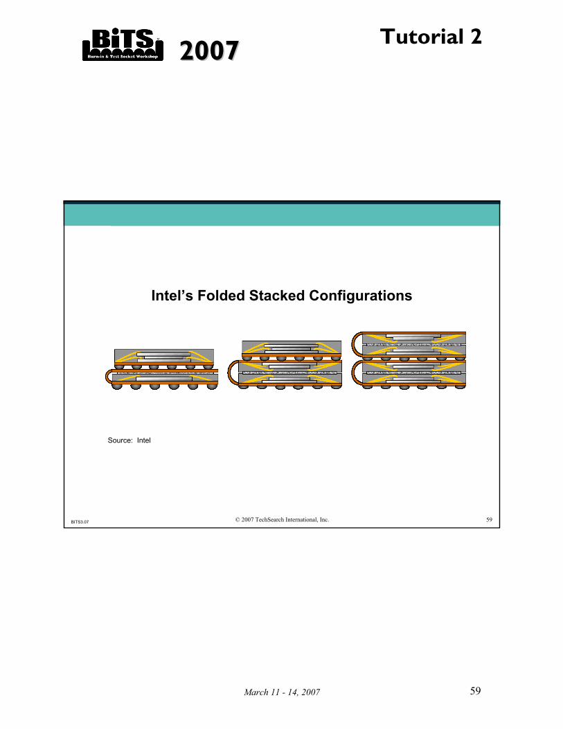
Intel’s Folded Stacked Configurations
Source: Intel

20072007Tutorial 2
March 11 - 14, 2007 60
BITS3.07 © 2007 TechSearch International, Inc. 60
Intel’s SiP in Motorola’s E680 Tri-band phone
• Folded flex technology has been adopted in Motorola’s E680 Tri-band phone
• Folded flex uses two-metal layer tape
20072007Tutorial 2
March 11 - 14, 2007 61
BITS3.07 © 2007 TechSearch International, Inc. 61
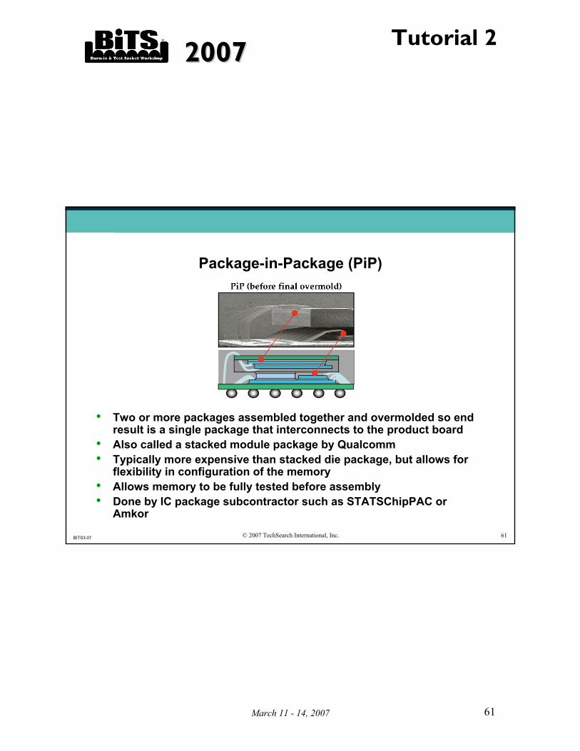
Package-in-Package (PiP)
• Two or more packages assembled together and overmolded so end result is a single package that interconnects to the product board
• Also called a stacked module package by Qualcomm• Typically more expensive than stacked die package, but allows for
flexibility in configuration of the memory• Allows memory to be fully tested before assembly• Done by IC package subcontractor such as STATSChipPAC or
Amkor

20072007Tutorial 2
March 11 - 14, 2007 62
BITS3.07 © 2007 TechSearch International, Inc. 62
Stacked Module Package (SMP)
Source: Qualcomm.
20072007Tutorial 2
March 11 - 14, 2007 63
BITS3.07 © 2007 TechSearch International, Inc. 63
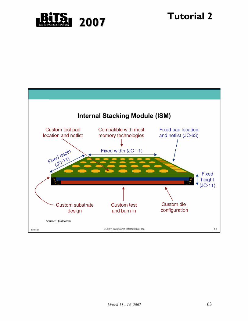
Internal Stacking Module (ISM)
Source: Qualcomm

20072007Tutorial 2
March 11 - 14, 2007 64
BITS3.07 © 2007 TechSearch International, Inc. 64
SIP Engine Package Comparison
Source: QualcommNote: QCT = Qualcomm CDMA Technologies, where CDMA = Code Division Multiple Access
20072007Tutorial 2
March 11 - 14, 2007 65
BITS3.07 © 2007 TechSearch International, Inc. 65
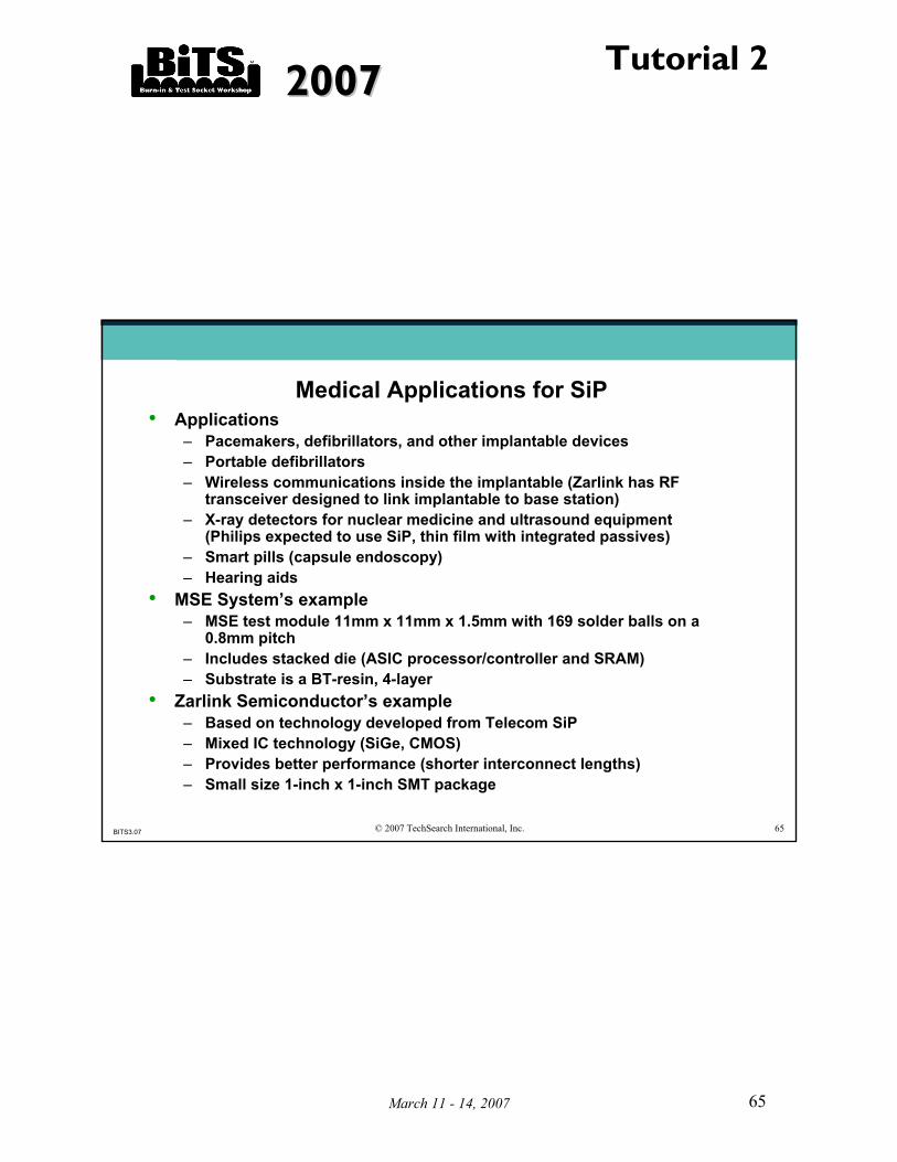
Medical Applications for SiP• Applications
– Pacemakers, defibrillators, and other implantable devices– Portable defibrillators– Wireless communications inside the implantable (Zarlink has RF
transceiver designed to link implantable to base station)– X-ray detectors for nuclear medicine and ultrasound equipment
(Philips expected to use SiP, thin film with integrated passives)– Smart pills (capsule endoscopy)– Hearing aids
• MSE System’s example– MSE test module 11mm x 11mm x 1.5mm with 169 solder balls on a
0.8mm pitch– Includes stacked die (ASIC processor/controller and SRAM)– Substrate is a BT-resin, 4-layer
• Zarlink Semiconductor’s example– Based on technology developed from Telecom SiP– Mixed IC technology (SiGe, CMOS)– Provides better performance (shorter interconnect lengths)– Small size 1-inch x 1-inch SMT package
20072007Tutorial 2
March 11 - 14, 2007 66
BITS3.07 © 2007 TechSearch International, Inc. 66
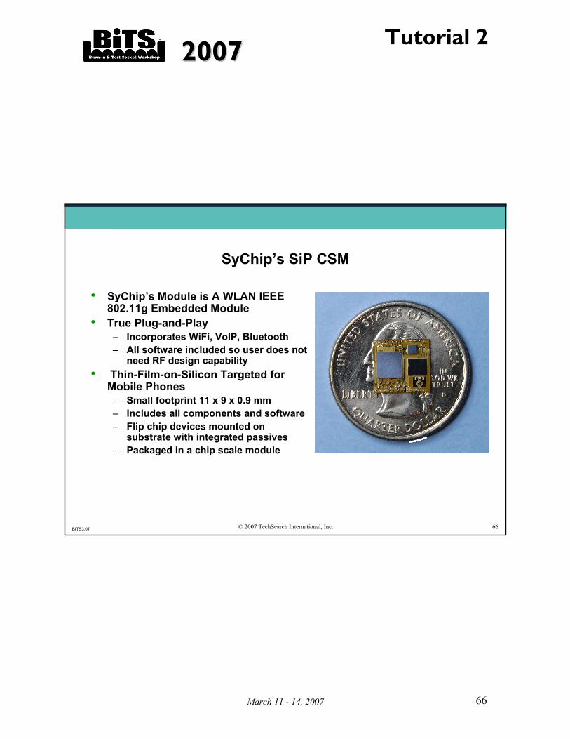
SyChip’s SiP CSM
• SyChip’s Module is A WLAN IEEE 802.11g Embedded Module
• True Plug-and-Play– Incorporates WiFi, VoIP, Bluetooth – All software included so user does not
need RF design capability• Thin-Film-on-Silicon Targeted for
Mobile Phones– Small footprint 11 x 9 x 0.9 mm– Includes all components and software– Flip chip devices mounted on
substrate with integrated passives– Packaged in a chip scale module

20072007Tutorial 2
March 11 - 14, 2007 67
BITS3.07 © 2007 TechSearch International, Inc. 67
Freescale’s New RCP SiP Technology

20072007Tutorial 2
March 11 - 14, 2007 68
BITS3.07 © 2007 TechSearch International, Inc. 68

20072007Tutorial 2
March 11 - 14, 2007 69
BITS3.07 © 2007 TechSearch International, Inc. 69
Typical Ring & Plate FCBGA Cross Section

20072007Tutorial 2
March 11 - 14, 2007 70
BITS3.07 © 2007 TechSearch International, Inc. 70
Flip Chip Bump Family
C4 (high T), eutectic (low T)
Au Bump with ACF
High T Solder to Laminate
Au Bump with ICA
ACF
High T solder
Low T solder
Au bump
Conductive adhesive
Polymer Flip Chip
Conductive adhesive bump

20072007Tutorial 2
March 11 - 14, 2007 71
BITS3.07 © 2007 TechSearch International, Inc. 71
Solder Bump Flip Chip
• Die size up to 24 mm• I/O count 1,000s• Minimum I/O pitch 150 microns• Bump diameter <150 microns typical• Bump height 100 microns typical• Package height 0.4 to 0.75 mm
Source: ASE
Source: SyChip
Source: Amkor
20072007Tutorial 2
March 11 - 14, 2007 72
BITS3.07 © 2007 TechSearch International, Inc. 72
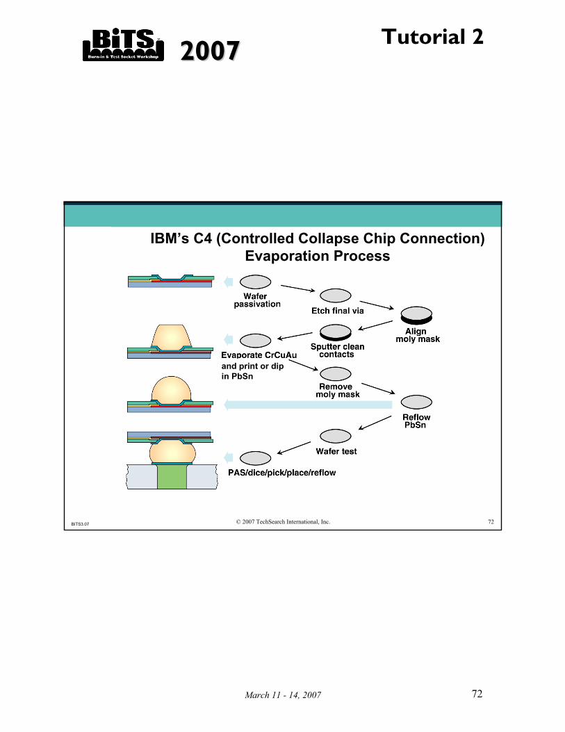
IBM’s C4 (Controlled Collapse Chip Connection) Evaporation Process
and print or dip in PbSn
20072007Tutorial 2
March 11 - 14, 2007 73
BITS3.07 © 2007 TechSearch International, Inc. 73
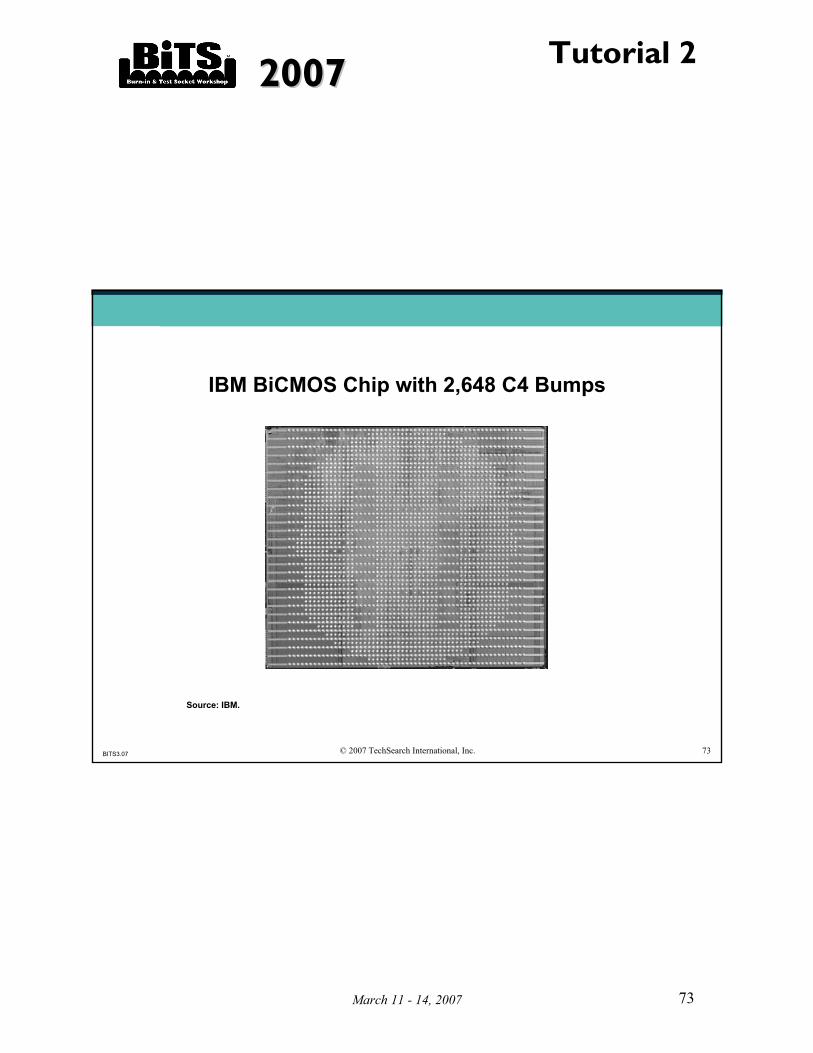
IBM BiCMOS Chip with 2,648 C4 Bumps
Source: IBM.
20072007Tutorial 2
March 11 - 14, 2007 74
BITS3.07 © 2007 TechSearch International, Inc. 74
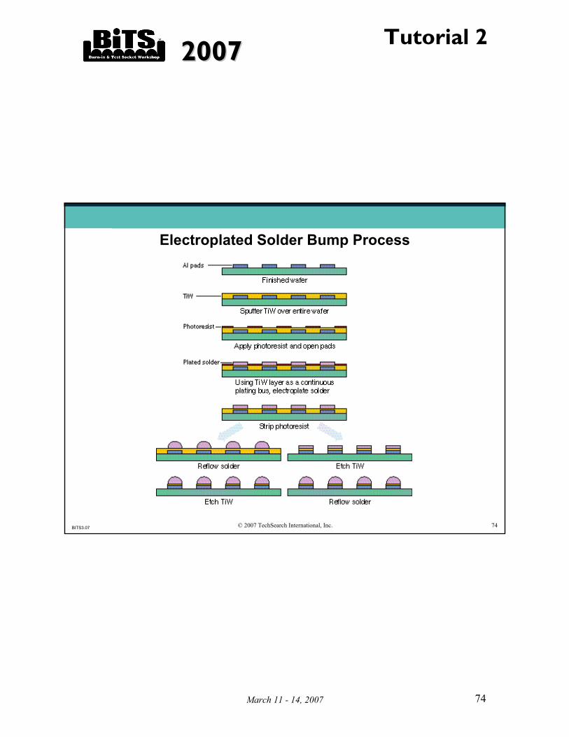
Electroplated Solder Bump Process
20072007Tutorial 2
March 11 - 14, 2007 75
BITS3.07 © 2007 TechSearch International, Inc. 75
Bumping Trends: Back to the Future• Early IBM bump was copper ball• Early bumps were copper posts with solder
– Citizen Watch– Automotive electronics
• Widespread adoption of the high-Pb bump using evaporation process (C4 bump)
– Licensed and put into production by Motorola, AMD– Cross licensing agreement with Intel, but plating process used in
production• Industry moved to electroplated bumps for flip chip
– Intel– TI– IBM, Motorola/Freescale Semiconductor, AMD, TSMC
• Some companies use printing, but plating favored for fine pitch• Copper pillar process being adopted by some companies

20072007Tutorial 2
March 11 - 14, 2007 76
BITS3.07 © 2007 TechSearch International, Inc. 76
Advanpack Solutions Pte Ltd.• Copper Pillar bump process
– Incoming wafer/preclean– Sputter Ti, Cu– Photoresist (2 passes 35µm each for 70µm thickness)– Expose/develop photoresist– Plate copper, solder– Resist strip to form column– Etch and reflow
• Pillar bump– Copper post is 100µm pillar (Cu post <65µm ±10 µm, Solder cap
30-35µm ±15 µm)– Less than 100µm pitch on pillar tip, eutectic solder or other on top– Bump pitch 150 µm, 46µm min. space– Promises better coplanarity, higher standoff, consistent flow under
die for underfill

20072007Tutorial 2
March 11 - 14, 2007 77
BITS3.07 © 2007 TechSearch International, Inc. 77
Chipworks Finds Intel’s Copper Pillar in Presler Processor(Internal Code Processor)
Source: Chipworks.
20072007Tutorial 2
March 11 - 14, 2007 78
BITS3.07 © 2007 TechSearch International, Inc. 78
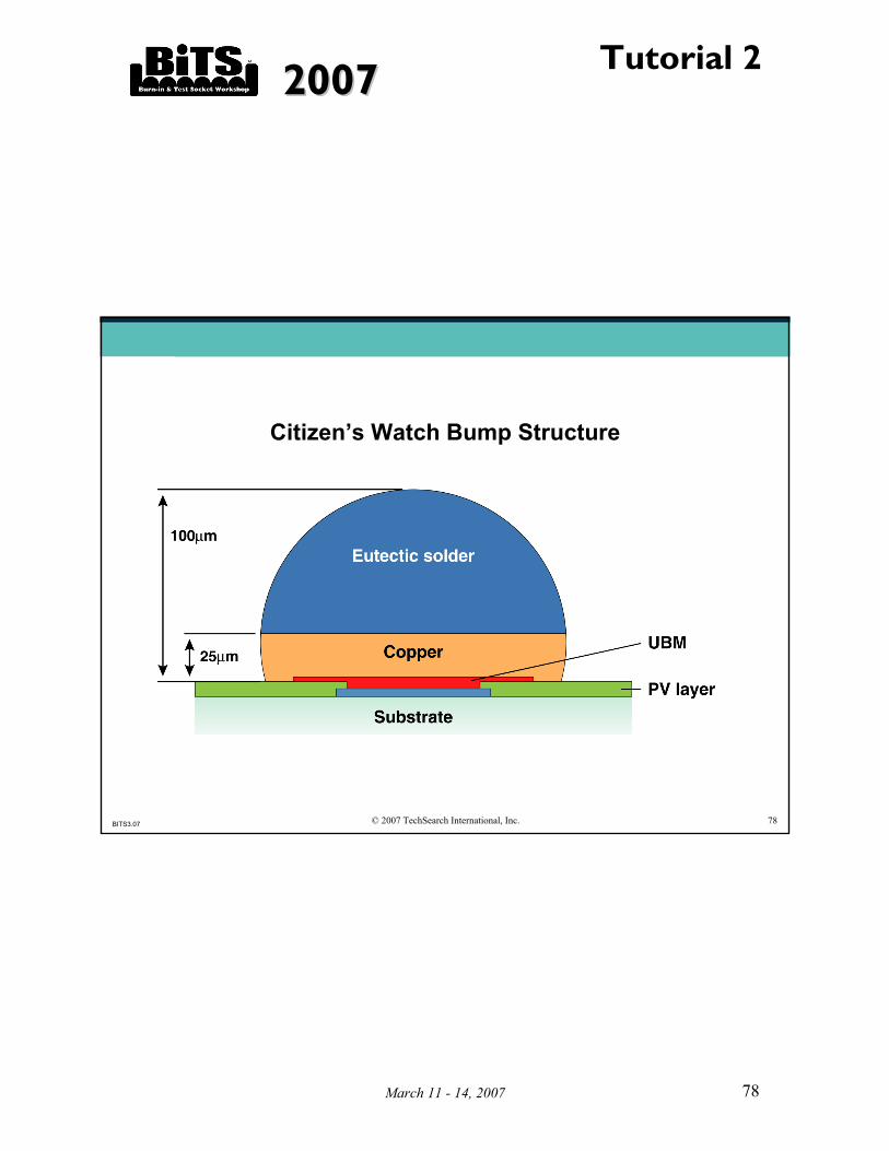
Citizen’s Watch Bump Structure
20072007Tutorial 2
March 11 - 14, 2007 79
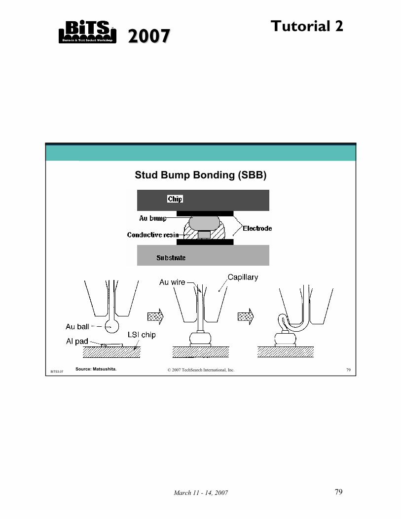
BITS3.07 © 2007 TechSearch International, Inc. 79
Stud Bump Bonding (SBB)
Source: Matsushita.

20072007Tutorial 2
March 11 - 14, 2007 80
BITS3.07 © 2007 TechSearch International, Inc. 80
Gold Wafer Bumping (Process)

20072007Tutorial 2
March 11 - 14, 2007 81
BITS3.07 © 2007 TechSearch International, Inc. 81
Gold Bumped Devices
• LCD drivers (main application)– Chip on glass (COG)– Chip on film (COF)– Tape automated bonding (TAB)
• Medical devices• RFID tags

20072007Tutorial 2
March 11 - 14, 2007 82
BITS3.07 © 2007 TechSearch International, Inc. 82
Delphi’s on-engine module
FC on Board (17)
20072007Tutorial 2
March 11 - 14, 2007 83
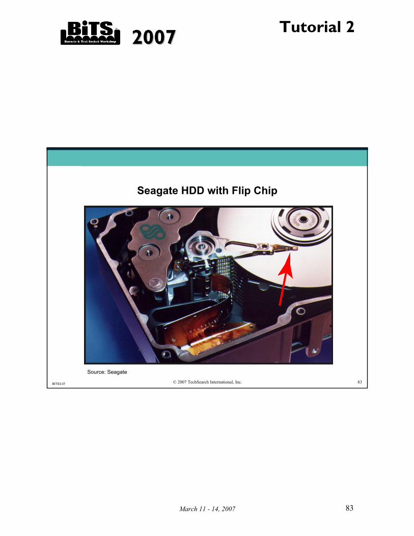
BITS3.07 © 2007 TechSearch International, Inc. 83
Seagate HDD with Flip Chip
Source: Seagate
20072007Tutorial 2
March 11 - 14, 2007 84
BITS3.07 © 2007 TechSearch International, Inc. 84
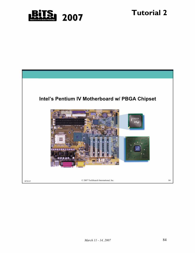
Intel’s Pentium IV Motherboard w/ PBGA Chipset

20072007Tutorial 2
March 11 - 14, 2007 85
BITS3.07 © 2007 TechSearch International, Inc. 85
Intel’s CPU for XBox Game Machine

20072007Tutorial 2
March 11 - 14, 2007 86
BITS3.07 © 2007 TechSearch International, Inc. 86
Xilinx VIRTEX-IIField Programmable Gate Array – FCBGA Pkg.

20072007Tutorial 2
March 11 - 14, 2007 87
BITS3.07 © 2007 TechSearch International, Inc. 87
PMC-Sierra Flip Chip

20072007Tutorial 2
March 11 - 14, 2007 88
BITS3.07 © 2007 TechSearch International, Inc. 88
Carsem’s FC on Leadframe (FCOL)

20072007Tutorial 2
March 11 - 14, 2007 89
BITS3.07 © 2007 TechSearch International, Inc. 89
Sony’s PoP
Source: Sony

20072007Tutorial 2
March 11 - 14, 2007 90
BITS3.07 © 2007 TechSearch International, Inc. 90
Solder Bump Pitch Trends
• DSP– TI was in production with 160µm bump pitch for three years– Found not to need tight bump pitch, current designs 180 µm– Finer pitch in future
• ASICs– Bump pitch of 200-180 µm in production today, moving to 150 µm in
the future• Network server processors
– Bump pitch of 180 µm moving to 150 µm
20072007Tutorial 2
March 11 - 14, 2007 91
BITS3.07 © 2007 TechSearch International, Inc. 91
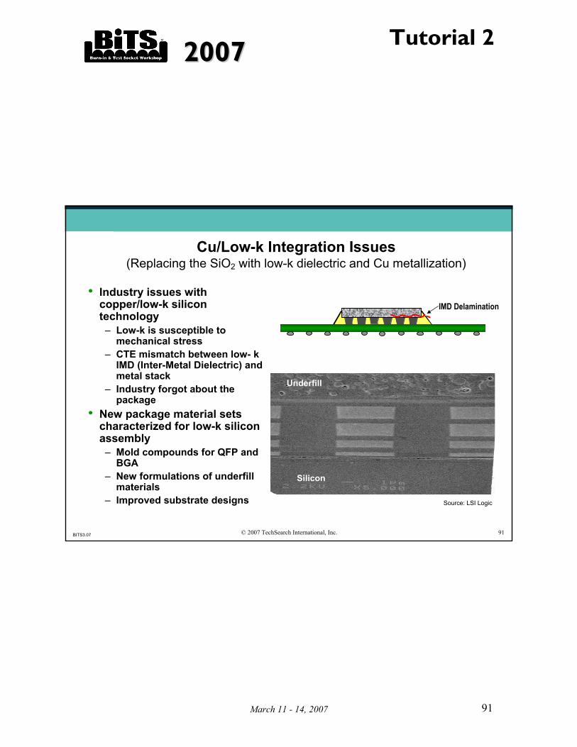
Cu/Low-k Integration Issues(Replacing the SiO2 with low-k dielectric and Cu metallization)
• Industry issues with copper/low-k silicon technology
– Low-k is susceptible to mechanical stress
– CTE mismatch between low- k IMD (Inter-Metal Dielectric) and metal stack
– Industry forgot about the package
• New package material sets characterized for low-k silicon assembly
– Mold compounds for QFP and BGA
– New formulations of underfill materials
– Improved substrate designs
IMD Delamination
Underfill
Silicon
Source: LSI Logic
20072007Tutorial 2
March 11 - 14, 2007 92
BITS3.07 © 2007 TechSearch International, Inc. 92

20072007Tutorial 2
March 11 - 14, 2007 93
BITS3.07 © 2007 TechSearch International, Inc. 93
Wafer Level Packages
• Die size <5 mm• I/O count 4 to 100• Minimum I/O pitch 400 microns• Bump diameter 250 to 500 microns• Bump height 180 to 400 microns• Package height 0.5 to 1.2 mm
Source: Texas Instruments
Source: Samsung
Source: International Rectifier

20072007Tutorial 2
March 11 - 14, 2007 94
BITS3.07 © 2007 TechSearch International, Inc. 94
Wafer Level CSP Categories
Package Construction CompaniesRedistribution/Bump ASE, Amkor/Unitive, Dallas
Semiconductor (Maxim), Hitachi,FlipChip International, NationalSemiconductor, PacTech,Renesas, Seik o Epson, SPIL,STMicroelectronics,STATSChipPAC
Metal post/bump with epoxy resin Casio, Fujitsu/Shinko Electric,Oki Electric, Fujikura
Encapsulated bond FormFactor, TesseraEncapsulated beam lead ShellCase (Xintec, Sanyo)
Source: TechSearch International, Inc.
20072007Tutorial 2
March 11 - 14, 2007 95
BITS3.07 © 2007 TechSearch International, Inc. 95
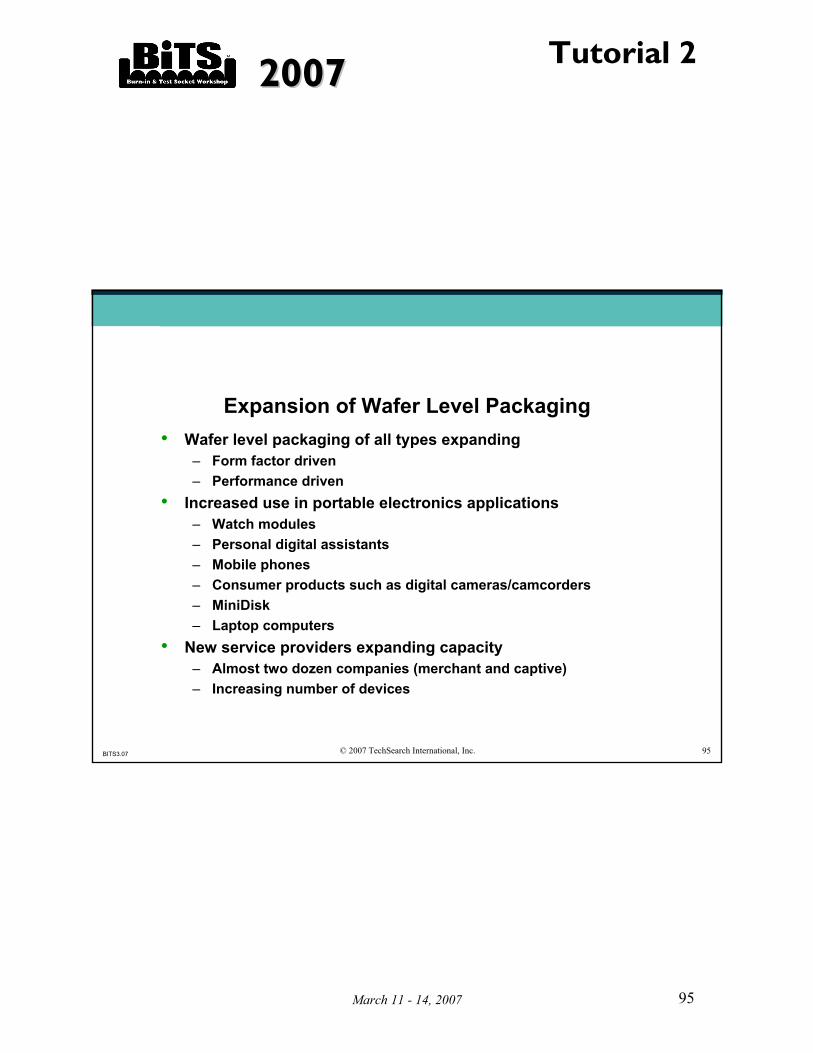
Expansion of Wafer Level Packaging• Wafer level packaging of all types expanding
– Form factor driven– Performance driven
• Increased use in portable electronics applications– Watch modules– Personal digital assistants– Mobile phones– Consumer products such as digital cameras/camcorders– MiniDisk– Laptop computers
• New service providers expanding capacity– Almost two dozen companies (merchant and captive)– Increasing number of devices

20072007Tutorial 2
March 11 - 14, 2007 96
BITS3.07 © 2007 TechSearch International, Inc. 96
Bourns’ Products in Sony Ericsson Phone
Source: Bourns
Integrated Passive Devices in WLP
20072007Tutorial 2
March 11 - 14, 2007 97
BITS3.07 © 2007 TechSearch International, Inc. 97
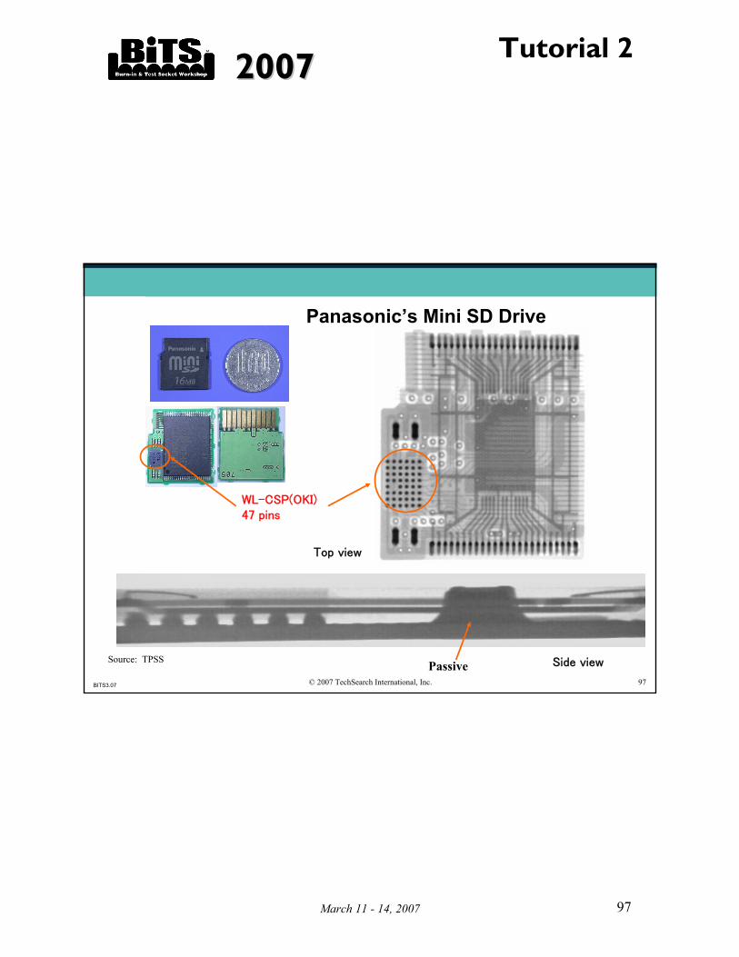
Panasonic’s Mini SD Drive
WL-CSP(OKI)47 pins
Top view
Side viewPassiveSource: TPSS
20072007Tutorial 2
March 11 - 14, 2007 98
BITS3.07 © 2007 TechSearch International, Inc. 98
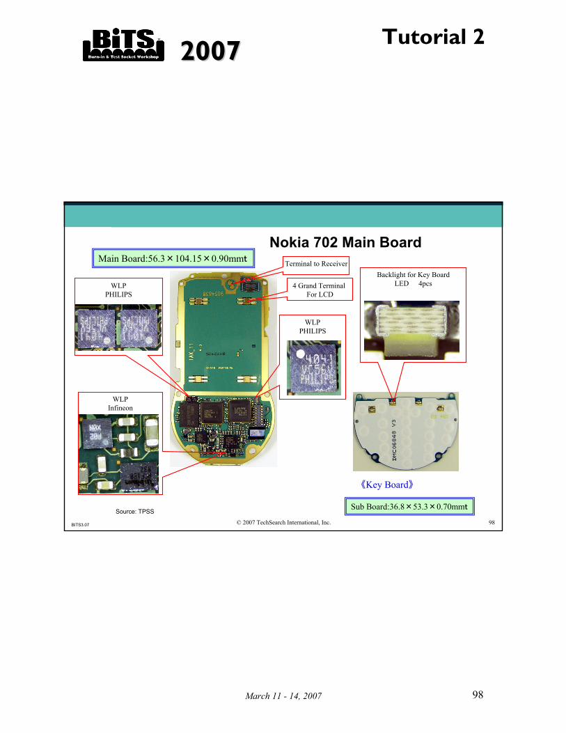
Backlight for Key BoardLED 4pcs
WLPPHILIPS
WLPPHILIPS
WLPInfineon
《Key Board》
Terminal to Receiver
4 Grand Terminal For LCD
Main Board:56.3×104.15×0.90mmt
Sub Board:36.8×53.3×0.70mmt
Nokia 702 Main Board
Source: TPSS

20072007Tutorial 2
March 11 - 14, 2007 99
BITS3.07 © 2007 TechSearch International, Inc. 99
FabFab..ProcessProcess
Die LevelDie LevelPackagingPackaging
Board LevelBoard LevelPackagingPackaging
SystemSystem
Advantages of WLP
Wafer Level Wafer Level PackagingPackaging
((FabFab. + WFP). + WFP)
Board LevelBoard LevelPackagingPackaging
SystemSystem
Conventional Packaging
WFP
Source: Samsung

20072007Tutorial 2
March 11 - 14, 2007 100
BITS3.07 © 2007 TechSearch International, Inc. 100
Advantages of WLP
<Lead Frame PKG(TSOP)> <BGA PKG(FBGA)> <WFP>
Comparison of Typical Package Type
Small form factor : Die size = Package sizeImprovement of electrical performance : • Shorter RDL length than Au wire
Process simplicity/Low cost : • Simple assembly process• Short TAT • No substrate : Wiring/BGA on the die
Advantages
For the same size die, package size is quite different!!
Source: Samsung
Samsung’s Wafer Level Fabricated PKG.

20072007Tutorial 2
March 11 - 14, 2007 101
BITS3.07 © 2007 TechSearch International, Inc. 101
Disadvantages
Large Die Difficulties • Solder Joint Reliability • Chip Crack during Die Handling The larger the worse.• Difficulties in Component Biz.
System Manufacturer (Customer) Friendliness/Preference:• Customers should be more careful in handling WFP dies. • Customers may invest new SMT equipments.
Disadvantages of WLP
Source: Samsung
20072007Tutorial 2
March 11 - 14, 2007 102
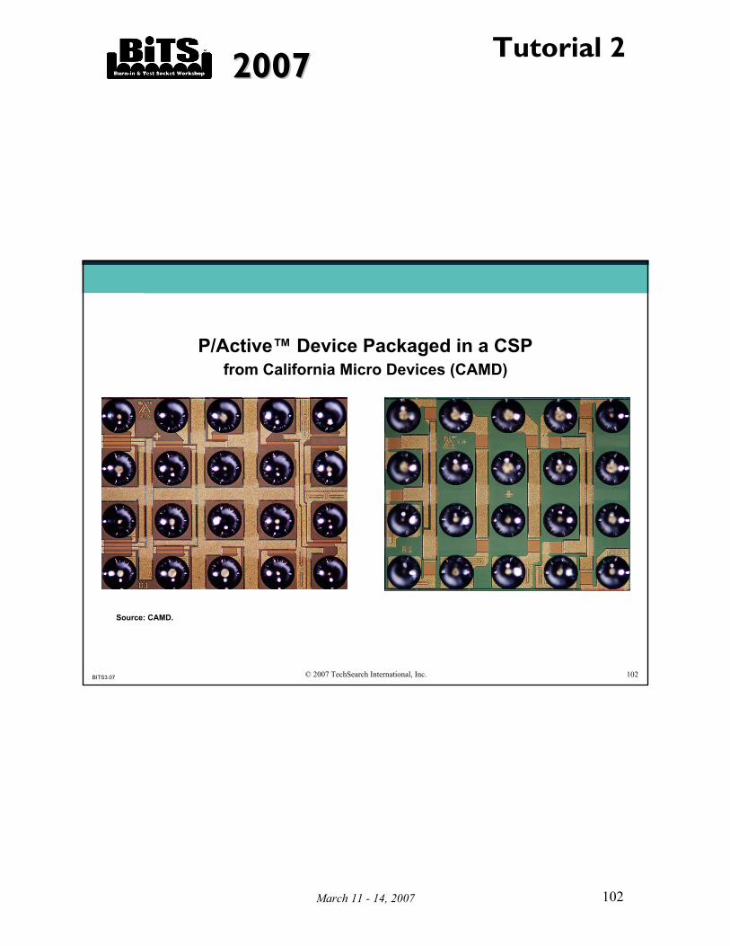
BITS3.07 © 2007 TechSearch International, Inc. 102
P/Active™ Device Packaged in a CSP from California Micro Devices (CAMD)
Source: CAMD.
20072007Tutorial 2
March 11 - 14, 2007 103
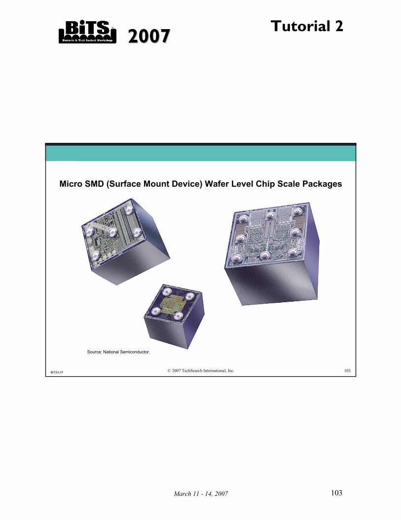
BITS3.07 © 2007 TechSearch International, Inc. 103
Micro SMD (Surface Mount Device) Wafer Level Chip Scale Packages
Source: National Semiconductor.

20072007Tutorial 2
March 11 - 14, 2007 104
BITS3.07 © 2007 TechSearch International, Inc. 104
International Rectifier’s FlipFET (Power MOSFET) WLP
Source: International Rectifier

20072007Tutorial 2
March 11 - 14, 2007 105
BITS3.07 © 2007 TechSearch International, Inc. 105
Tessera’s ShellOP Wafer Level Chip Size Package
Source: ShellCase.
(Glass-silicon-glass sandwich structure)

20072007Tutorial 2
March 11 - 14, 2007 106
BITS3.07 © 2007 TechSearch International, Inc. 106
Fujikura’s WLP
Source: Fujikura
20072007Tutorial 2
March 11 - 14, 2007 107
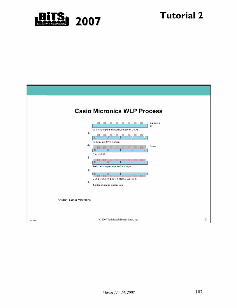
BITS3.07 © 2007 TechSearch International, Inc. 107
Casio Micronics WLP Process
Source: Casio Micronics

20072007Tutorial 2
March 11 - 14, 2007 108
BITS3.07 © 2007 TechSearch International, Inc. 108
Fujitsu’s Super CSP Structure
Source: TechSearch International, Inc.
20072007Tutorial 2
March 11 - 14, 2007 109
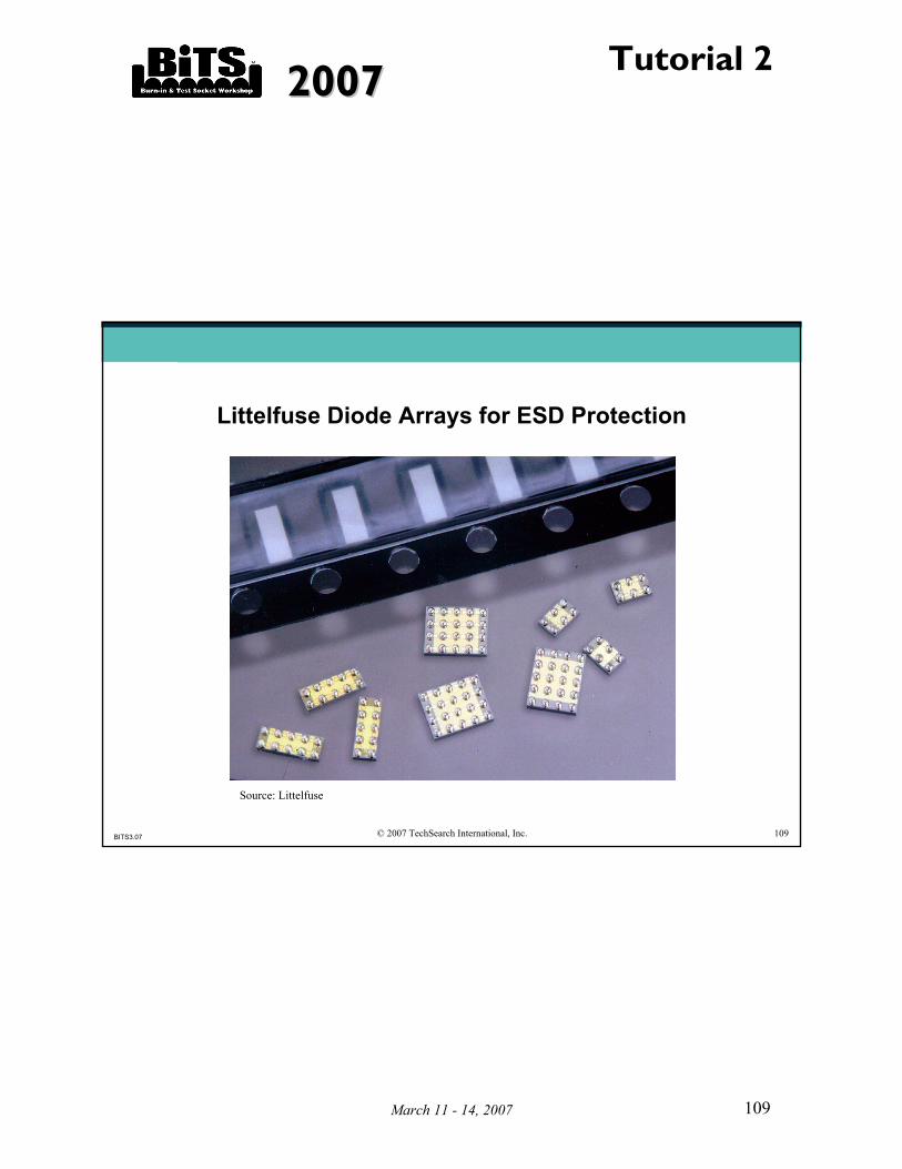
BITS3.07 © 2007 TechSearch International, Inc. 109
Littelfuse Diode Arrays for ESD Protection
Source: Littelfuse

20072007Tutorial 2
March 11 - 14, 2007 110
BITS3.07 © 2007 TechSearch International, Inc. 110
DRAM Package Trends
• Higher speed DRAM or modules that require higher density are increasingly using FBGA
• Graphics applications (higher speed) use FBGA package– Better electrical performance– Smaller size package so more memory on the module (number of
slots limited, so want more density per module)• Some DDR2 (Dynamic Data Rate) makers are using wafer level
packages– Micron shipped a limited number of DDR2 SDRAM in wafer level
package (uses bumps instead of wires)– Samsung announced DDR2 SDRAM in 60 I/O wafer level package– TwinMOS ships Twister module (SO-DIMM) with WLP
• DDR3 expected to use WLP or flip chip on laminate substrate, not wire bond

20072007Tutorial 2
March 11 - 14, 2007 111
BITS3.07 © 2007 TechSearch International, Inc. 111
WLP for DRAM
Future production of DDR3 is expected to use WLP.WLP provides better electrical performance and higher density on the module. Footprint changes with die shrinks and test are concerns.

20072007Tutorial 2
March 11 - 14, 2007 112
BITS3.07 © 2007 TechSearch International, Inc. 112
TechSearch International, Inc.(www.techsearchinc.com)
• Founded in 1987 by E. Jan Vardaman and based in Austin, Texas offering consulting services including:
– Semiconductor packaging and assembly trends
– Semiconductor packaging materials
– Market forecasts and technology licensing
• Research topics include flip chip, BGAs, CSPs (inc. stacked die and WLP), SiP, 3D Integration with through silicon vias (TSV)
• Analysts with mixture of materials science, chemistry, assembly and process development, reliability, marketing, economic, strategy, competitive analysis, and modeling backgrounds
• Extensive contacts (>15,000) throughout North America, Europe, Japan, China, Hong Kong, Taiwan, Korea, Singapore, Malaysia, Thailand, and The Philippines


