20 V, 300 mA, Low Noise, CMOS LDO Data Sheet ADP7102 · 20 V, 300 mA, Low Noise, CMOS LDO Data...
28
20 V, 300 mA, Low Noise, CMOS LDO Data Sheet ADP7102 Rev. E Document Feedback Information furnished by Analog Devices is believed to be accurate and reliable. However, no responsibility is assumed by Analog Devices for its use, nor for any infringements of patents or other rights of third parties that may result from its use. Specifications subject to change without notice. No license is granted by implication or otherwise under any patent or patent rights of Analog Devices. Trademarks and registered trademarks are the property of their respective owners. One Technology Way, P.O. Box 9106, Norwood, MA 02062-9106, U.S.A. Tel: 781.329.4700 ©2011–2015 Analog Devices, Inc. All rights reserved. Technical Support www.analog.com FEATURES Input voltage range: 3.3 V to 20 V Maximum output current: 300 mA Low noise: 15 μV rms for fixed output versions PSRR performance of 60 dB at 10 kHz, VOUT = 3.3 V Reverse current protection Low dropout voltage: 200 mV at 300 mA load Initial accuracy: ±0.8% Accuracy over line, load, and temperature: −2%, +1% Low quiescent current (VIN = 5 V), IGND = 750 μA with 300 mA load Low shutdown current: 40 μA at VIN = 12 V Stable with small 1 μF ceramic output capacitor 7 fixed output voltage options: 1.5 V, 1.8 V, 2.5 V, 3 V, 3.3 V, 5 V, and 9 V Adjustable output from 1.22 V to VIN − VDO Foldback current limit and thermal overload protection User programmable precision UVLO/enable Power-good indicator 8-lead LFCSP and 8-lead SOIC packages APPLICATIONS Regulation to noise sensitive applications: ADC, DAC circuits, precision amplifiers, high frequency oscillators, clocks, and phase-locked loops Communications and infrastructure Medical and healthcare Industrial and instrumentation TYPICAL APPLICATION CIRCUITS VOUT = 5V VIN = 8V PG VOUT VIN PG GND SENSE EN/ UVLO RPG 100kΩ R2 100kΩ R1 100kΩ COUT 1μF CIN 1μF ON OFF + + 09506-001 Figure 1. ADP7102 with Fixed Output Voltage, 5 V VOUT = 5V VIN = 8V PG VOUT VIN PG GND ADJ EN/ UVLO RPG 100kΩ R4 100kΩ R3 100kΩ COUT 1μF CIN 1μF ON OFF + + R2 13kΩ R1 40.2kΩ 09506-002 Figure 2. ADP7102 with Adjustable Output Voltage, 5 V GENERAL DESCRIPTION The ADP7102 is a CMOS, low dropout linear regulator that operates from 3.3 V to 20 V and provides up to 300 mA of output current. This high input voltage LDO is ideal for regulation of high performance analog and mixed signal circuits operating from 19 V to 1.22 V rails. Using an advanced proprietary architecture, it provides high power supply rejection, low noise, and achieves excellent line and load transient response with just a small 1 μF ceramic output capacitor. The ADP7102 is available in seven fixed output voltage options and an adjustable version, which allows output voltages that range from 1.22 V to VIN − VDO via an external feedback divider. The ADP7102 output noise voltage is 15 μV rms and is independent of the output voltage. A digital power-good output allows power system monitors to check the health of the output voltage. A user programmable precision undervoltage lockout function facilitates sequencing of multiple power supplies. The ADP7102 is available in 8-lead, 3 mm × 3 mm LFCSP and 8-lead SOIC packages. The LFCSP offers a very compact solution and also provides excellent thermal performance for applications requiring up to 300 mA of output current in a small, low profile footprint.
Transcript of 20 V, 300 mA, Low Noise, CMOS LDO Data Sheet ADP7102 · 20 V, 300 mA, Low Noise, CMOS LDO Data...
20 V, 300 mA, Low Noise, CMOS LDOData Sheet ADP7102
Rev. E Document Feedback Information furnished by Analog Devices is believed to be accurate and reliable. However, no responsibility is assumed by Analog Devices for its use, nor for any infringements of patents or other rights of third parties that may result from its use. Specifications subject to change without notice. No license is granted by implication or otherwise under any patent or patent rights of Analog Devices. Trademarks and registered trademarks are the property of their respective owners.
One Technology Way, P.O. Box 9106, Norwood, MA 02062-9106, U.S.A.Tel: 781.329.4700 ©2011–2015 Analog Devices, Inc. All rights reserved. Technical Support www.analog.com
FEATURES Input voltage range: 3.3 V to 20 V Maximum output current: 300 mA Low noise: 15 μV rms for fixed output versions PSRR performance of 60 dB at 10 kHz, VOUT = 3.3 V Reverse current protection Low dropout voltage: 200 mV at 300 mA load Initial accuracy: ±0.8% Accuracy over line, load, and temperature: −2%, +1% Low quiescent current (VIN = 5 V), IGND = 750 μA with 300 mA load Low shutdown current: 40 μA at VIN = 12 V Stable with small 1 μF ceramic output capacitor 7 fixed output voltage options: 1.5 V, 1.8 V, 2.5 V, 3 V, 3.3 V,
5 V, and 9 V Adjustable output from 1.22 V to VIN − VDO Foldback current limit and thermal overload protection User programmable precision UVLO/enable Power-good indicator 8-lead LFCSP and 8-lead SOIC packages
APPLICATIONS Regulation to noise sensitive applications: ADC, DAC
circuits, precision amplifiers, high frequency oscillators, clocks, and phase-locked loops
Communications and infrastructure Medical and healthcare Industrial and instrumentation
TYPICAL APPLICATION CIRCUITS
VOUT = 5VVIN = 8V
PG
VOUTVIN
PG
GND
SENSE
EN/UVLO
RPG100kΩ
R2100kΩ
R1100kΩ
COUT1µF
CIN1µF
ONOFF
++
0950
6-00
1
Figure 1. ADP7102 with Fixed Output Voltage, 5 V
VOUT = 5VVIN = 8V
PG
VOUTVIN
PG
GND
ADJ
EN/UVLO
RPG100kΩ
R4100kΩ
R3100kΩ
COUT1µF
CIN1µF
ONOFF
++
R213kΩ
R140.2kΩ
0950
6-00
2
Figure 2. ADP7102 with Adjustable Output Voltage, 5 V
GENERAL DESCRIPTION The ADP7102 is a CMOS, low dropout linear regulator that operates from 3.3 V to 20 V and provides up to 300 mA of output current. This high input voltage LDO is ideal for regulation of high performance analog and mixed signal circuits operating from 19 V to 1.22 V rails. Using an advanced proprietary architecture, it provides high power supply rejection, low noise, and achieves excellent line and load transient response with just a small 1 μF ceramic output capacitor.
The ADP7102 is available in seven fixed output voltage options and an adjustable version, which allows output voltages that range from 1.22 V to VIN − VDO via an external feedback divider.
The ADP7102 output noise voltage is 15 μV rms and is independent of the output voltage. A digital power-good output allows power system monitors to check the health of the output voltage. A user programmable precision undervoltage lockout function facilitates sequencing of multiple power supplies.
The ADP7102 is available in 8-lead, 3 mm × 3 mm LFCSP and 8-lead SOIC packages. The LFCSP offers a very compact solution and also provides excellent thermal performance for applications requiring up to 300 mA of output current in a small, low profile footprint.
ADP7102 Data Sheet
Rev. E | Page 2 of 28
TABLE OF CONTENTS Features .............................................................................................. 1
Applications ....................................................................................... 1
Typical Application Circuits ............................................................ 1
General Description ......................................................................... 1
Revision History ............................................................................... 2
Specifications ..................................................................................... 3
Input and Output Capacitor, Recommended Specifications .. 4
Absolute Maximum Ratings ............................................................ 5
Thermal Data ................................................................................ 5
ESD Caution .................................................................................. 5
Pin Configurations and Function Descriptions ........................... 6
Typical Performance Characteristics ............................................. 7
Theory of Operation ...................................................................... 17
Applications Information .............................................................. 18
Capacitor Selection .................................................................... 18
Programable Undervoltage Lockout (UVLO) ........................... 19
Power-Good Feature .................................................................. 20
Noise Reduction of the Adjustable ADP7102 ............................ 20
Current Limit and Thermal Overload Protection ................. 21
Thermal Considerations ............................................................ 21
Printed Circuit Board Layout Considerations ............................ 24
Outline Dimensions ....................................................................... 25
Ordering Guide .......................................................................... 26
REVISION HISTORY 9/15—Rev. D to Rev. E Changes to Figure 60 ...................................................................... 17 5/14—Rev. C to Rev. D Changed UVLO Threshold Rising Typ Parameter from 1.23 V to 1.22 V; Table 1 ............................................................................... 4 Changes to Power Good Section .................................................. 20 Updated Outline Dimensions ....................................................... 26 8/13—Rev. B to Rev. C Changes to Table 3 ............................................................................ 5 2/13—Rev. A to Rev. B Changes to Noise Reduction of the Adjustable ADP7102 Section .............................................................................................. 20 11/11—Rev. 0 to Rev. A Changes to Figure 50 ...................................................................... 14 10/11—Revision 0: Initial Version
Data Sheet ADP7102
Rev. E | Page 3 of 28
SPECIFICATIONS VIN = (VOUT + 1 V) or 3.3 V (whichever is greater), EN = VIN, IOUT = 10 mA, CIN = COUT = 1 μF, TA = 25°C, unless otherwise noted.
Table 1. Parameter Symbol Test Conditions/Comments Min Typ Max Unit INPUT VOLTAGE RANGE VIN 3.3 20 V OPERATING SUPPLY CURRENT IGND IOUT = 100 μA, VIN = 10 V 400 μA IOUT = 100 μA, VIN = 10 V, TJ = −40°C to +125°C 900 μA IOUT = 10 mA, VIN = 10 V 450 μA IOUT = 10 mA, VIN = 10 V, TJ = −40°C to +125°C 1050 μA IOUT = 150 mA, VIN = 10 V 650 μA IOUT = 150 mA, VIN = 10 V, TJ = −40°C to +125°C 1250 μA IOUT = 300 mA, VIN = 10 V 750 μA IOUT = 300 mA, VIN = 10 V, TJ = −40°C to +125°C 1400 μA SHUTDOWN CURRENT IGND-SD EN = GND, VIN = 12 V 40 μA EN = GND, VIN = 12 V, TJ = −40°C to +125°C 75 μA INPUT REVERSE CURRENT IREV-INPUT EN = GND, VIN = 0 V, VOUT = 20 V 0.3 μA EN = GND, VIN = 0 V, VOUT = 20 V, TJ = −40°C to +125°C 5 μA OUTPUT VOLTAGE ACCURACY
Fixed Output Voltage Accuracy
VOUT IOUT = 10 mA −0.8 +0.8 %
1 mA < IOUT < 300 mA, VIN = (VOUT + 1 V) to 20 V, TJ = −40°C to +125°C
−2 +1 %
Adjustable Output Voltage Accuracy
VADJ IOUT = 10 mA 1.21 1.22 1.23 V
1 mA < IOUT < 300 mA, VIN = (VOUT + 1 V) to 20 V, TJ = −40°C to +125°C
1.196 1.232 V
LINE REGULATION ∆VOUT/∆VIN VIN = (VOUT + 1 V) to 20 V, TJ = −40°C to +125°C −0.015 +0.015 %/V LOAD REGULATION1 ∆VOUT/∆IOUT IOUT = 1 mA to 300 mA 0.2 %/A IOUT = 1 mA to 300 mA, TJ = −40°C to +125°C 1.0 %/A ADJ INPUT BIAS CURRENT ADJI-BIAS 1 mA < IOUT < 300 mA, VIN = (VOUT + 1 V) to 20 V,
ADJ connected to VOUT 10 nA
SENSE INPUT BIAS CURRENT SENSEI-BIAS 1 mA < IOUT < 300 mA, VIN = (VOUT + 1 V) to 20 V, SENSE connected to VOUT, VOUT = 1.5 V
1 μA
DROPOUT VOLTAGE2 VDROPOUT IOUT = 10 mA 20 mV IOUT = 10 mA, TJ = −40°C to +125°C 40 mV IOUT = 150 mA 100 mV IOUT = 150 mA, TJ = −40°C to +125°C 175 mV IOUT = 300 mA 200 mV IOUT = 300 mA, TJ = −40°C to +125°C 325 mV START-UP TIME3 tSTART-UP VOUT = 5 V 800 μs CURRENT-LIMIT THRESHOLD4 ILIMIT 450 575 750 mA PG OUTPUT LOGIC LEVEL
PG Output Logic High PGHIGH IOH < 1 μA 1.0 V PG Output Logic Low PGLOW IOL < 2 mA 0.4 V
PG OUTPUT THRESHOLD Output Voltage Falling PGFALL −9.2 % Output Voltage Rising PGRISE −6.5 %
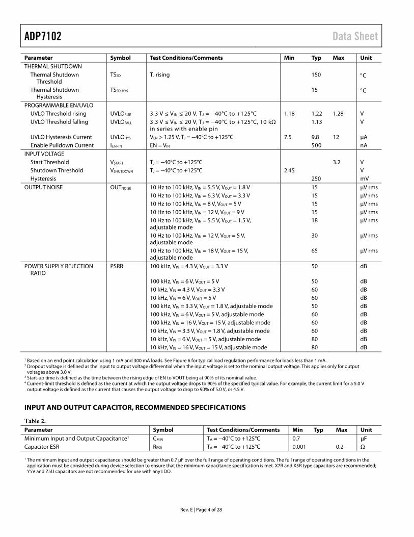
ADP7102 Data Sheet
Rev. E | Page 4 of 28
Parameter Symbol Test Conditions/Comments Min Typ Max Unit THERMAL SHUTDOWN
Thermal Shutdown Threshold
TSSD TJ rising 150 C
Thermal Shutdown Hysteresis
TSSD-HYS 15 C
PROGRAMMABLE EN/UVLO UVLO Threshold rising UVLORISE 3.3 V ≤ VIN ≤ 20 V, TJ = −40°C to +125°C 1.18 1.22 1.28 V UVLO Threshold falling UVLOFALL 3.3 V ≤ VIN ≤ 20 V, TJ = −40°C to +125°C, 10 kΩ
in series with enable pin 1.13 V
UVLO Hysteresis Current UVLOHYS VEN > 1.25 V, TJ = −40°C to +125°C 7.5 9.8 12 μA Enable Pulldown Current IEN-IN EN = VIN 500 nA
INPUT VOLTAGE Start Threshold VSTART TJ = −40°C to +125°C 3.2 V Shutdown Threshold VSHUTDOWN TJ = −40°C to +125°C 2.45 V Hysteresis 250 mV
OUTPUT NOISE OUTNOISE 10 Hz to 100 kHz, VIN = 5.5 V, VOUT = 1.8 V 15 μV rms 10 Hz to 100 kHz, VIN = 6.3 V, VOUT = 3.3 V 15 μV rms 10 Hz to 100 kHz, VIN = 8 V, VOUT = 5 V 15 μV rms 10 Hz to 100 kHz, VIN = 12 V, VOUT = 9 V 15 μV rms 10 Hz to 100 kHz, VIN = 5.5 V, VOUT = 1.5 V,
adjustable mode 18 μV rms
10 Hz to 100 kHz, VIN = 12 V, VOUT = 5 V, adjustable mode
30 μV rms
10 Hz to 100 kHz, VIN = 18 V, VOUT = 15 V, adjustable mode
65 μV rms
POWER SUPPLY REJECTION RATIO
PSRR 100 kHz, VIN = 4.3 V, VOUT = 3.3 V 50 dB
100 kHz, VIN = 6 V, VOUT = 5 V 50 dB 10 kHz, VIN = 4.3 V, VOUT = 3.3 V 60 dB 10 kHz, VIN = 6 V, VOUT = 5 V 60 dB 100 kHz, VIN = 3.3 V, VOUT = 1.8 V, adjustable mode 50 dB 100 kHz, VIN = 6 V, VOUT = 5 V, adjustable mode 60 dB 100 kHz, VIN = 16 V, VOUT = 15 V, adjustable mode 60 dB 10 kHz, VIN = 3.3 V, VOUT = 1.8 V, adjustable mode 60 dB 10 kHz, VIN = 6 V, VOUT = 5 V, adjustable mode 80 dB 10 kHz, VIN = 16 V, VOUT = 15 V, adjustable mode 80 dB 1 Based on an end point calculation using 1 mA and 300 mA loads. See Figure 6 for typical load regulation performance for loads less than 1 mA. 2 Dropout voltage is defined as the input to output voltage differential when the input voltage is set to the nominal output voltage. This applies only for output
voltages above 3.0 V. 3 Start-up time is defined as the time between the rising edge of EN to VOUT being at 90% of its nominal value. 4 Current-limit threshold is defined as the current at which the output voltage drops to 90% of the specified typical value. For example, the current limit for a 5.0 V
output voltage is defined as the current that causes the output voltage to drop to 90% of 5.0 V, or 4.5 V.
INPUT AND OUTPUT CAPACITOR, RECOMMENDED SPECIFICATIONS
Table 2. Parameter Symbol Test Conditions/Comments Min Typ Max Unit Minimum Input and Output Capacitance1 CMIN TA = −40°C to +125°C 0.7 μF Capacitor ESR RESR TA = −40°C to +125°C 0.001 0.2 Ω 1 The minimum input and output capacitance should be greater than 0.7 μF over the full range of operating conditions. The full range of operating conditions in the
application must be considered during device selection to ensure that the minimum capacitance specification is met. X7R and X5R type capacitors are recommended; Y5V and Z5U capacitors are not recommended for use with any LDO.
Data Sheet ADP7102
Rev. E | Page 5 of 28
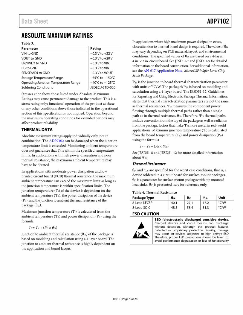
ABSOLUTE MAXIMUM RATINGS Table 3. Parameter Rating VIN to GND −0.3 V to +22 V VOUT to GND −0.3 V to +20 V EN/UVLO to GND −0.3 V to VIN PG to GND −0.3 V to VIN SENSE/ADJ to GND −0.3 V to VOUT Storage Temperature Range −65°C to +150°C Operating Junction Temperature Range −40°C to +125°C Soldering Conditions JEDEC J-STD-020
Stresses at or above those listed under Absolute Maximum Ratings may cause permanent damage to the product. This is a stress rating only; functional operation of the product at these or any other conditions above those indicated in the operational section of this specification is not implied. Operation beyond the maximum operating conditions for extended periods may affect product reliability.
THERMAL DATA Absolute maximum ratings apply individually only, not in combination. The ADP7102 can be damaged when the junction temperature limit is exceeded. Monitoring ambient temperature does not guarantee that TJ is within the specified temperature limits. In applications with high power dissipation and poor thermal resistance, the maximum ambient temperature may have to be derated.
In applications with moderate power dissipation and low printed circuit board (PCB) thermal resistance, the maximum ambient temperature can exceed the maximum limit as long as the junction temperature is within specification limits. The junction temperature (TJ) of the device is dependent on the ambient temperature (TA), the power dissipation of the device (PD), and the junction to ambient thermal resistance of the package (θJA).
Maximum junction temperature (TJ) is calculated from the ambient temperature (TA) and power dissipation (PD) using the formula
TJ = TA + (PD × θJA)
Junction to ambient thermal resistance (θJA) of the package is based on modeling and calculation using a 4-layer board. The junction to ambient thermal resistance is highly dependent on the application and board layout.
In applications where high maximum power dissipation exists, close attention to thermal board design is required. The value of θJA may vary, depending on PCB material, layout, and environmental conditions. The specified values of θJA are based on a 4-layer, 4 in. × 3 in. circuit board. See JESD51-7 and JESD51-9 for detailed information on the board construction. For additional information, see the AN-617 Application Note, MicroCSP Wafer Level Chip Scale Package.
ΨJB is the junction to board thermal characterization parameter with units of °C/W. The package’s ΨJB is based on modeling and calculation using a 4-layer board. The JESD51-12, Guidelines for Reporting and Using Electronic Package Thermal Information, states that thermal characterization parameters are not the same as thermal resistances. ΨJB measures the component power flowing through multiple thermal paths rather than a single path as in thermal resistance, θJB. Therefore, ΨJB thermal paths include convection from the top of the package as well as radiation from the package, factors that make ΨJB more useful in real-world applications. Maximum junction temperature (TJ) is calculated from the board temperature (TB) and power dissipation (PD) using the formula
TJ = TB + (PD × ΨJB)
See JESD51-8 and JESD51-12 for more detailed information about ΨJB.
Thermal Resistance
θJA and ΨJB are specified for the worst case conditions, that is, a device soldered in a circuit board for surface-mount packages. θJC is a parameter for surface-mount packages with top mounted heat sinks. θJC is presented here for reference only.
Table 4. Thermal Resistance Package Type θJA θJC ΨJB Unit 8-Lead LFCSP 40.1 27.1 17.2 °C/W 8-Lead SOIC 48.5 58.4 31.3 °C/W
ESD CAUTION
ADP7102 Data Sheet
Rev. E | Page 6 of 28
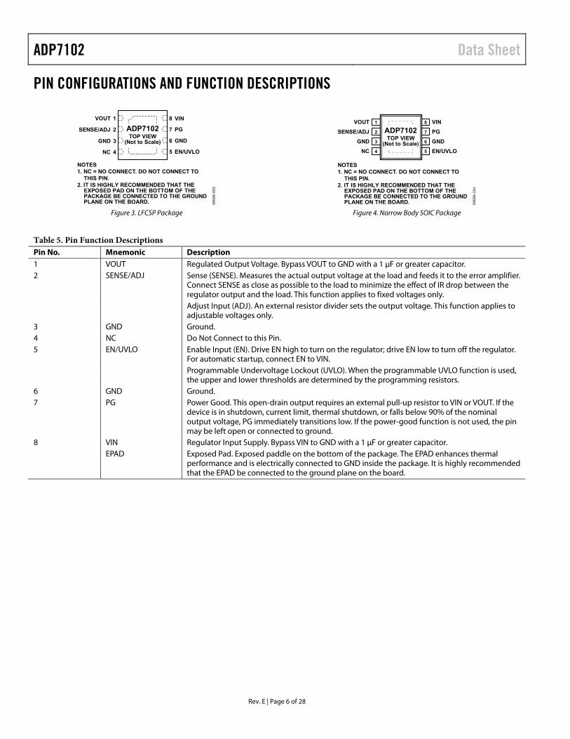
PIN CONFIGURATIONS AND FUNCTION DESCRIPTIONS
NOTES1. NC = NO CONNECT. DO NOT CONNECT TO THIS PIN.
2. IT IS HIGHLY RECOMMENDED THAT THE EXPOSED PAD ON THE BOTTOM OF THE PACKAGE BE CONNECTED TO THE GROUND PLANE ON THE BOARD.
3GND
4NC
1VOUT
2SENSE/ADJ
6 GND
5 EN/UVLO
8 VIN
7 PGADP7102TOP VIEW
(Not to Scale)
0950
6-00
3
Figure 3. LFCSP Package
NOTES1. NC = NO CONNECT. DO NOT CONNECT TO THIS PIN.2. IT IS HIGHLY RECOMMENDED THAT THE EXPOSED PAD ON THE BOTTOM OF THE PACKAGE BE CONNECTED TO THE GROUND PLANE ON THE BOARD.
VOUT 1
SENSE/ADJ 2
GND 3
NC 4
VIN8
PG7
GND6
EN/UVLO5
ADP7102TOP VIEW
(Not to Scale)
0950
6-10
4
Figure 4. Narrow Body SOIC Package
Table 5. Pin Function Descriptions Pin No. Mnemonic Description 1 VOUT Regulated Output Voltage. Bypass VOUT to GND with a 1 μF or greater capacitor. 2 SENSE/ADJ Sense (SENSE). Measures the actual output voltage at the load and feeds it to the error amplifier.
Connect SENSE as close as possible to the load to minimize the effect of IR drop between the regulator output and the load. This function applies to fixed voltages only.
Adjust Input (ADJ). An external resistor divider sets the output voltage. This function applies to adjustable voltages only.
3 GND Ground. 4 NC Do Not Connect to this Pin. 5 EN/UVLO Enable Input (EN). Drive EN high to turn on the regulator; drive EN low to turn off the regulator.
For automatic startup, connect EN to VIN. Programmable Undervoltage Lockout (UVLO). When the programmable UVLO function is used,
the upper and lower thresholds are determined by the programming resistors. 6 GND Ground. 7 PG Power Good. This open-drain output requires an external pull-up resistor to VIN or VOUT. If the
device is in shutdown, current limit, thermal shutdown, or falls below 90% of the nominal output voltage, PG immediately transitions low. If the power-good function is not used, the pin may be left open or connected to ground.
8 VIN Regulator Input Supply. Bypass VIN to GND with a 1 μF or greater capacitor. EPAD Exposed Pad. Exposed paddle on the bottom of the package. The EPAD enhances thermal
performance and is electrically connected to GND inside the package. It is highly recommended that the EPAD be connected to the ground plane on the board.
Data Sheet ADP7102
Rev. E | Page 7 of 28
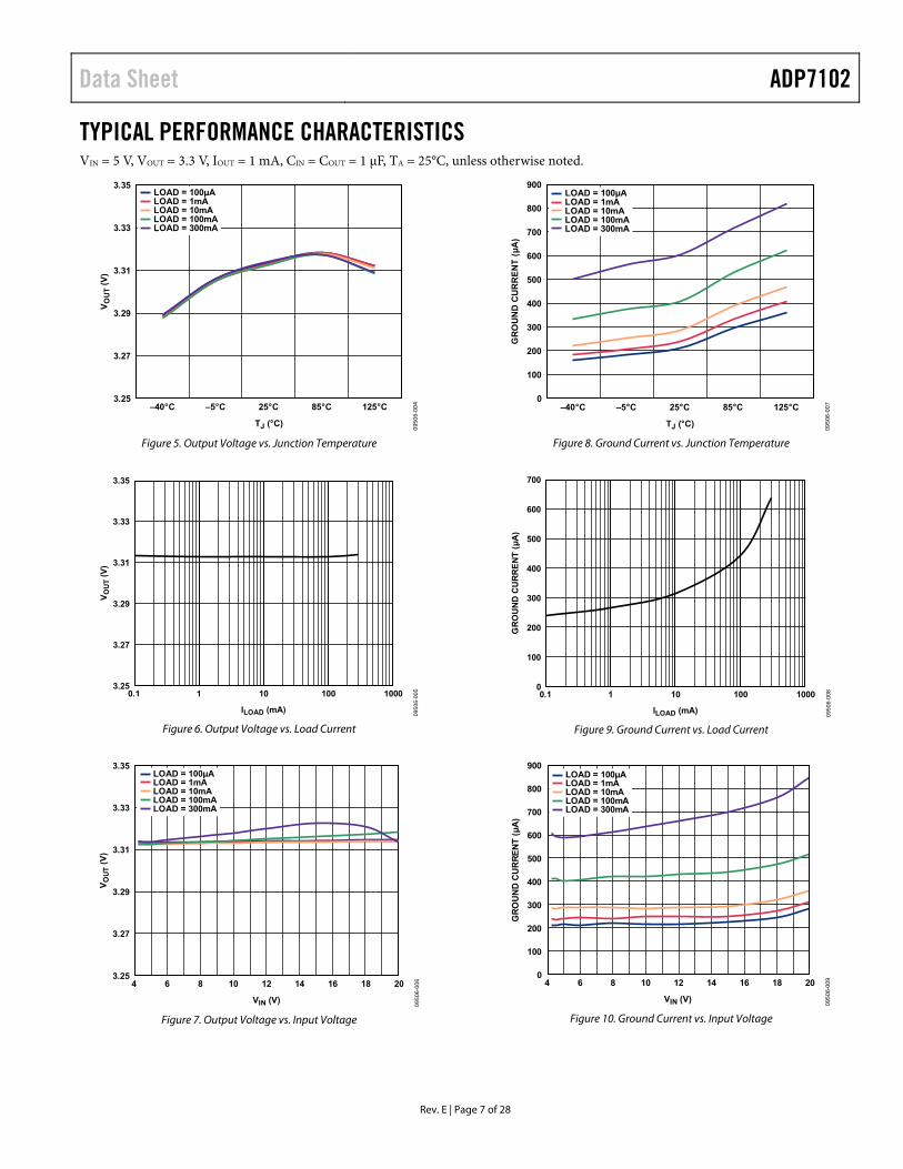
TYPICAL PERFORMANCE CHARACTERISTICS VIN = 5 V, VOUT = 3.3 V, IOUT = 1 mA, CIN = COUT = 1 μF, TA = 25°C, unless otherwise noted.
3.25
3.27
3.29
3.31
3.33
3.35
VO
UT (
V)
–40°C –5°C 25°C 85°C 125°C
TJ (°C)
LOAD = 100µALOAD = 1mALOAD = 10mALOAD = 100mALOAD = 300mA
0950
6-00
4
Figure 5. Output Voltage vs. Junction Temperature
3.25
3.27
3.29
3.31
3.33
3.35
0.1 1 10 100 1000
VO
UT (
V)
ILOAD (mA) 0950
6-00
5
Figure 6. Output Voltage vs. Load Current
3.25
3.27
3.29
3.31
3.33
3.35
4 6 8 10 12 14 16 18 20
VO
UT (
V)
VIN (V)
LOAD = 100µALOAD = 1mALOAD = 10mALOAD = 100mALOAD = 300mA
0950
6-00
6
Figure 7. Output Voltage vs. Input Voltage
0
100
200
300
400
500
600
700
800
900
GR
OU
ND
CU
RR
EN
T(µ
A)
–40°C –5°C 25°C 85°C 125°C
TJ (°C)
LOAD = 100µALOAD = 1mALOAD = 10mALOAD = 100mALOAD = 300mA
0950
6-00
7
Figure 8. Ground Current vs. Junction Temperature
0
100
200
300
400
500
600
700
0.1 1 10 100 1000
GR
OU
ND
CU
RR
EN
T (
µA
)
ILOAD (mA)
0950
6-00
8
Figure 9. Ground Current vs. Load Current
0
100
200
300
400
500
600
700
800
900
64 8 10 12 14 16 18 20
GR
OU
ND
CU
RR
EN
T(µ
A)
VIN (V)
LOAD = 100µALOAD = 1mALOAD = 10mALOAD = 100mALOAD = 300mA
0950
6-00
9
Figure 10. Ground Current vs. Input Voltage
ADP7102 Data Sheet
Rev. E | Page 8 of 28
0
20
40
60
80
100
120
140
160
–50 –25 0 25 50 75 100 125
SH
UT
DO
WN
CU
RR
EN
T (
µA
)
TEMPERATURE (°C)
3.3V4.0V6.0V8.0V12.0V20.0V
0950
6-01
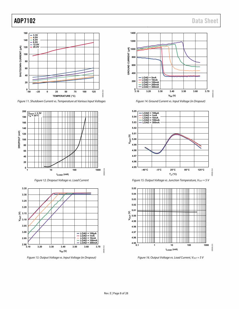
0Figure 11. Shutdown Current vs. Temperature at Various Input Voltages
0
20
40
60
80
100
120
140
160
180
200
1 10 100 1000
DR
OP
OU
T (
mV
)
ILOAD (mA)
VOUT = 3.3VTA = 25°C
0950
6-01
1
Figure 12. Dropout Voltage vs. Load Current
2.90
2.95
3.00
3.05
3.10
3.15
3.20
3.25
3.30
3.35
3.10 3.20 3.30 3.40 3.50 3.60 3.70
VO
UT (
V)
VIN (V)
0950
6-01
2
LOAD = 100µALOAD = 1mALOAD = 10mALOAD = 100mALOAD = 300mA
Figure 13. Output Voltage vs. Input Voltage (in Dropout)
0
200
400
600
800
1000
1200
1400
3.10 3.20 3.30 3.40 3.50 3.60 3.70
GR
OU
ND
CU
RR
EN
T (
µA
)
VIN (V)
0950
6-01
3
LOAD = 5mALOAD = 10mALOAD = 100mALOAD = 200mALOAD = 300mA
Figure 14. Ground Current vs. Input Voltage (in Dropout)
4.95
4.96
4.97
4.98
4.99
5.00
5.01
5.02
5.03
5.04
5.05
VO
UT (
V)
–40°C –5°C 25°C 85°C 125°C
TJ (°C)
LOAD = 100µALOAD = 1mALOAD = 10mALOAD = 100mALOAD = 300mA
0950
6-01
4
Figure 15. Output Voltage vs. Junction Temperature, VOUT = 5 V
4.95
4.96
4.97
4.98
4.99
5.00
5.01
5.02
5.03
5.04
5.05
0.1 1 10 100 1000
VO
UT (
V)
ILOAD (mA)
0950
6-01
5
Figure 16. Output Voltage vs. Load Current, VOUT = 5 V
Data Sheet ADP7102
Rev. E | Page 9 of 28
4.95
4.96
4.97
4.98
4.99
5.00
5.01
5.02
5.03
5.04
5.05
6 8 10 12 14 16 18 20
VO
UT (
V)
VIN (V)
LOAD = 100µALOAD = 1mALOAD = 10mALOAD = 100mALOAD = 300mA
0950
6-01
6
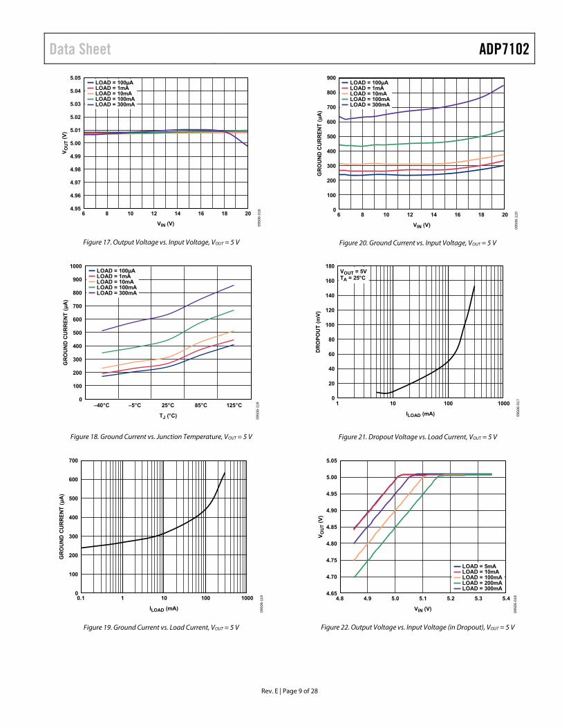
Figure 17. Output Voltage vs. Input Voltage, VOUT = 5 V
0950
6-11
8
GR
OU
ND
CU
RR
EN
T (
µA
)
0
100
200
300
400
500
600
700
800
900
1000
–40°C –5°C 25°C 85°C 125°C
TJ (°C)
LOAD = 100µALOAD = 1mALOAD = 10mALOAD = 100mALOAD = 300mA
Figure 18. Ground Current vs. Junction Temperature, VOUT = 5 V
0
100
200
300
400
500
600
700
0.1 1 10 100 1000
GR
OU
ND
CU
RR
EN
T (
µA
)
ILOAD (mA)
0950
6-11
9
Figure 19. Ground Current vs. Load Current, VOUT = 5 V
0
100
200
300
400
500
600
700
800
900
GR
OU
ND
CU
RR
EN
T (
µA
)
6 8 10 12 14 16 18 20
VIN (V)
LOAD = 100µALOAD = 1mALOAD = 10mALOAD = 100mALOAD = 300mA
0950
6-12
0
Figure 20. Ground Current vs. Input Voltage, VOUT = 5 V
0
20
40
60
80
100
120
140
160
180
1 10 100 1000
DR
OP
OU
T (
mV
)
ILOAD (mA)
VOUT = 5VTA = 25°C
0950
6-01
7
Figure 21. Dropout Voltage vs. Load Current, VOUT = 5 V
4.65
4.70
4.75
4.80
4.85
4.90
4.95
5.00
5.05
4.8 4.9 5.0 5.1 5.2 5.3 5.4
VO
UT (
V)
VIN (V)
0950
6-01
8
LOAD = 5mALOAD = 10mALOAD = 100mALOAD = 200mALOAD = 300mA
Figure 22. Output Voltage vs. Input Voltage (in Dropout), VOUT = 5 V
ADP7102 Data Sheet
Rev. E | Page 10 of 28
VIN (V)
–500
0
500
1000
1500
2000
2500
4.80 4.90 5.00 5.10 5.20 5.30 5.40
GR
OU
ND
CU
RR
EN
T (
µA
)
0950
6-01
9
LOAD = 5mALOAD = 10mALOAD = 100mALOAD = 200mALOAD = 300mA
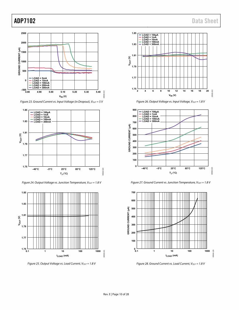
Figure 23. Ground Current vs. Input Voltage (in Dropout), VOUT = 5 V
1.75
1.77
1.79
1.81
1.83
1.85
VO
UT (
V)
LOAD = 100µALOAD = 1mALOAD = 10mALOAD = 100mALOAD = 300mA
–40°C –5°C 25°C 85°C 125°C
TJ (°C)
0950
6-02
0
Figure 24. Output Voltage vs. Junction Temperature, VOUT = 1.8 V
1.75
1.77
1.79
1.81
1.83
1.85
0.1 1 10 100 1000
VO
UT (
V)
ILOAD (mA)
0950
6-02
1
Figure 25. Output Voltage vs. Load Current, VOUT = 1.8 V
1.75
1.77
1.79
1.81
1.83
1.85
2 4 6 8 10 12 14 16 18 20
VO
UT (
V)
VIN (V)
LOAD = 100µALOAD = 1mALOAD = 10mALOAD = 100mALOAD = 300mA
0950
6-02
2
Figure 26. Output Voltage vs. Input Voltage, VOUT = 1.8 V
0
100
200
300
400
500
600
700
800
900
–40°C –5°C 25°C 85°C 125°C
GR
OU
ND
CU
RR
EN
T (
µA
)
TJ (°C)
LOAD = 100µALOAD = 1mALOAD = 10mALOAD = 100mALOAD = 300mA
0950
6-02
3
Figure 27. Ground Current vs. Junction Temperature, VOUT = 1.8 V
0
100
200
300
400
500
600
700
0.1 1 10 100 1000
GR
OU
ND
CU
RR
EN
T (
µA
)
ILOAD (mA)
0950
6-12
8
Figure 28. Ground Current vs. Load Current, VOUT = 1.8 V
Data Sheet ADP7102
Rev. E | Page 11 of 28
GR
OU
ND
CU
RR
EN
T (
µA
)
VIN (V)
0
200
400
600
800
1000
1200
2 4 6 8 10 12 14 16 18 20
LOAD = 100µALOAD = 1mALOAD = 10mALOAD = 100mALOAD = 300mA
0950
6-12
9
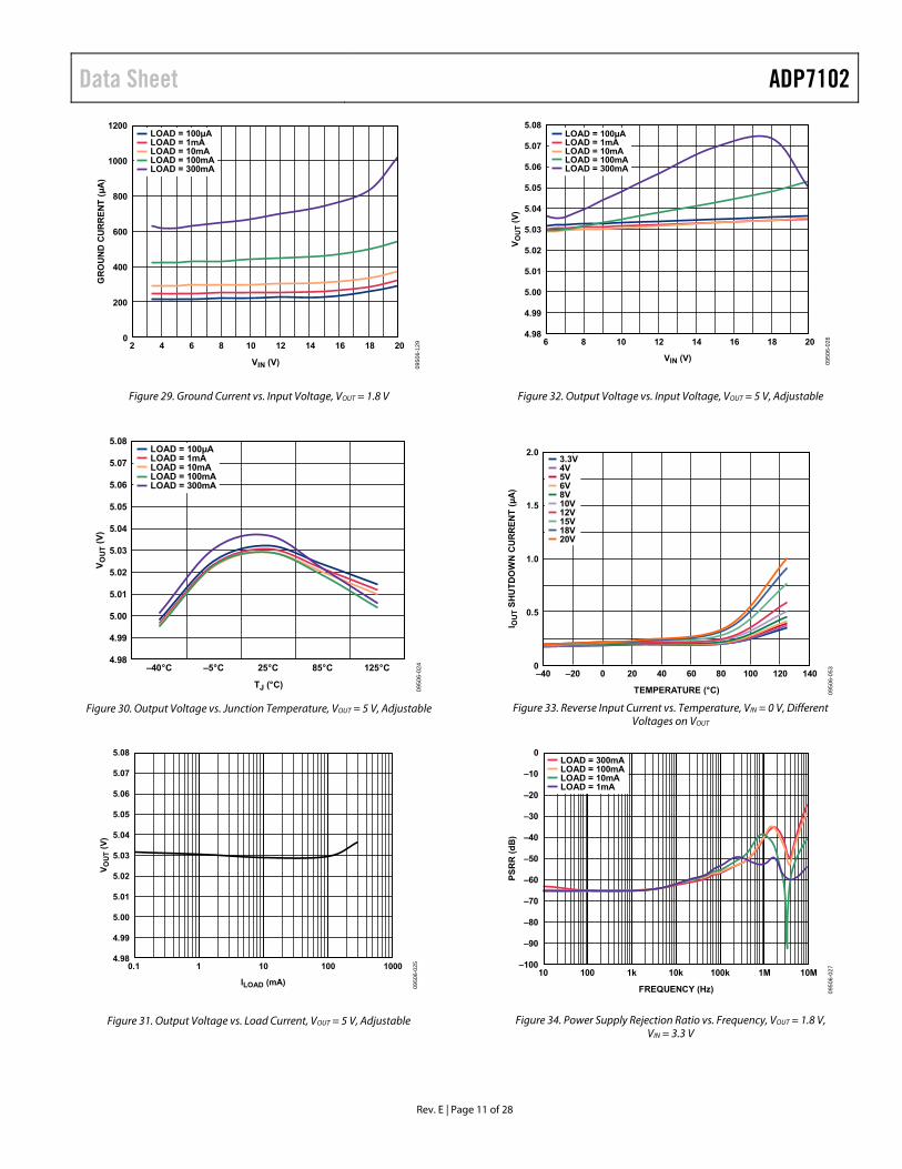
Figure 29. Ground Current vs. Input Voltage, VOUT = 1.8 V
4.98
4.99
5.00
5.01
5.02
5.03
5.04
5.05
5.06
5.07
5.08
VO
UT (
V)
LOAD = 100µALOAD = 1mALOAD = 10mALOAD = 100mALOAD = 300mA
–40°C –5°C 25°C 85°C 125°C
TJ (°C)
0950
6-02
4
Figure 30. Output Voltage vs. Junction Temperature, VOUT = 5 V, Adjustable
4.98
4.99
5.00
5.01
5.02
5.03
5.04
5.05
5.06
5.07
5.08
0.1 1 10 100 1000
VO
UT (
V)
ILOAD (mA)
0950
6-02
5
Figure 31. Output Voltage vs. Load Current, VOUT = 5 V, Adjustable
4.98
4.99
5.00
5.01
5.02
5.03
5.04
5.05
5.06
5.07
5.08
6 8 10 12 14 16 18 20
VO
UT (
V)
VIN (V)
LOAD = 100µALOAD = 1mALOAD = 10mALOAD = 100mALOAD = 300mA
0950
6-02
6
Figure 32. Output Voltage vs. Input Voltage, VOUT = 5 V, Adjustable
0
0.5
1.0
1.5
2.0
–40 –20 0 20 40 60 80 100 120 140
I OU
T S
HU
TD
OW
N C
UR
RE
NT
(µ
A)
TEMPERATURE (°C)
3.3V4V5V6V8V10V12V15V18V20V
0950
6-05
3
Figure 33. Reverse Input Current vs. Temperature, VIN = 0 V, Different Voltages on VOUT
–100
–90
–80
–70
–60
–50
–40
–30
–20
–10
0
10 100 1k 10k 100k 1M 10M
PS
RR
(d
B)
FREQUENCY (Hz)
LOAD = 300mALOAD = 100mALOAD = 10mALOAD = 1mA
0950
6-02
7
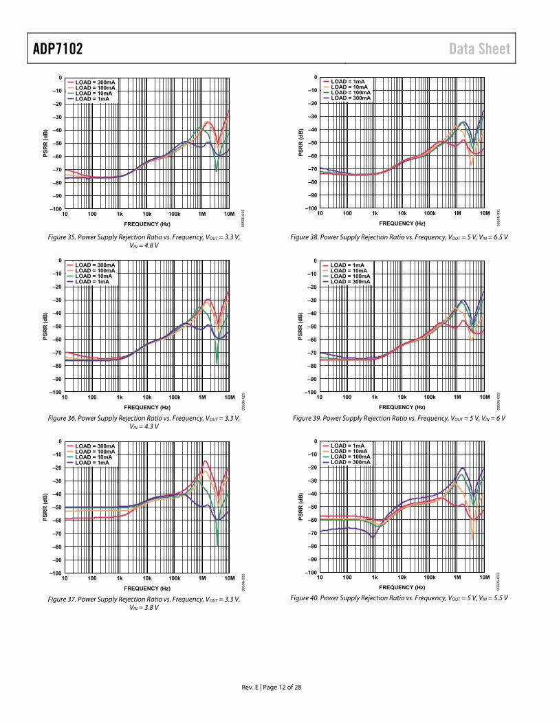
Figure 34. Power Supply Rejection Ratio vs. Frequency, VOUT = 1.8 V, VIN = 3.3 V
ADP7102 Data Sheet
Rev. E | Page 12 of 28
–100
–90
–80
–70
–60
–50
–40
–30
–20
–10
0
10 100 1k 10k 100k 1M 10M
PS
RR
(d
B)
FREQUENCY (Hz)
LOAD = 300mALOAD = 100mALOAD = 10mALOAD = 1mA
0950
6-02
8
Figure 35. Power Supply Rejection Ratio vs. Frequency, VOUT = 3.3 V, VIN = 4.8 V
–100
–90
–80
–70
–60
–50
–40
–30
–20
–10
0
10 100 1k 10k 100k 1M 10M
PS
RR
(d
B)
FREQUENCY (Hz)
LOAD = 300mALOAD = 100mALOAD = 10mALOAD = 1mA
0950
6-02
9
Figure 36. Power Supply Rejection Ratio vs. Frequency, VOUT = 3.3 V, VIN = 4.3 V
–100
–90
–80
–70
–60
–50
–40
–30
–20
–10
0
10 100 1k 10k 100k 1M 10M
PS
RR
(d
B)
FREQUENCY (Hz)
LOAD = 300mALOAD = 100mALOAD = 10mALOAD = 1mA
0950
6-03
0
Figure 37. Power Supply Rejection Ratio vs. Frequency, VOUT = 3.3 V, VIN = 3.8 V
–100
–90
–80
–70
–60
–50
–40
–30
–20
–10
0
10 100 1k 10k 100k 1M 10M
PS
RR
(d
B)
FREQUENCY (Hz)
LOAD = 1mALOAD = 10mALOAD = 100mALOAD = 300mA
0950
6-03
1
Figure 38. Power Supply Rejection Ratio vs. Frequency, VOUT = 5 V, VIN = 6.5 V
–100
–90
–80
–70
–60
–50
–40
–30
–20
–10
0
10 100 1k 10k 100k 1M 10M
PS
RR
(d
B)
FREQUENCY (Hz)
LOAD = 1mALOAD = 10mALOAD = 100mALOAD = 300mA
0950
6-03
2
Figure 39. Power Supply Rejection Ratio vs. Frequency, VOUT = 5 V, VIN = 6 V
–100
–90
–80
–70
–60
–50
–40
–30
–20
–10
0
10 100 1k 10k 100k 1M 10M
PS
RR
(d
B)
FREQUENCY (Hz)
LOAD = 1mALOAD = 10mALOAD = 100mALOAD = 300mA
0950
6-03
3
Figure 40. Power Supply Rejection Ratio vs. Frequency, VOUT = 5 V, VIN = 5.5 V
Data Sheet ADP7102
Rev. E | Page 13 of 28
–100
–90
–80
–70
–60
–50
–40
–30
–20
–10
0
10 100 1k 10k 100k 1M 10M
PS
RR
(d
B)
FREQUENCY (Hz)
LOAD = 1mALOAD = 10mALOAD = 100mALOAD = 300mA
0950
6-03
4
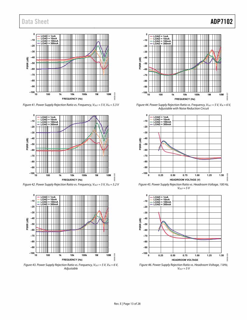
Figure 41. Power Supply Rejection Ratio vs. Frequency, VOUT = 5 V, VIN = 5.3 V
–100
–90
–80
–70
–60
–50
–40
–30
–20
–10
0
10 100 1k 10k 100k 1M 10M
PS
RR
(d
B)
FREQUENCY (Hz)
LOAD = 1mALOAD = 10mALOAD = 100mALOAD = 300mA
0950
6-03
5
Figure 42. Power Supply Rejection Ratio vs. Frequency, VOUT = 5 V, VIN = 5.2 V
–100
–90
–80
–70
–60
–50
–40
–30
–20
–10
0
10 100 1k 10k 100k 1M 10M
PS
RR
(d
B)
FREQUENCY (Hz)
LOAD = 1mALOAD = 10mALOAD = 100mALOAD = 300mA
0950
6-03
6
Figure 43. Power Supply Rejection Ratio vs. Frequency, VOUT = 5 V, VIN = 6 V, Adjustable
–100
–90
–80
–70
–60
–50
–40
–30
–20
–10
0
10 100 1k 10k 100k 1M 10M
PS
RR
(d
B)
FREQUENCY (Hz)
LOAD = 1mALOAD = 10mALOAD = 100mALOAD = 300mA
0950
6-03
7
Figure 44. Power Supply Rejection Ratio vs. Frequency, VOUT = 5 V, VIN = 6 V, Adjustable with Noise Reduction Circuit
–100
–90
–80
–70
–60
–50
–40
–30
–20
–10
0
0 0.25 0.50 0.75 1.00 1.25 1.50
PS
RR
(d
B)
HEADROOM VOLTAGE (V)
LOAD = 1mALOAD = 10mALOAD = 100mALOAD = 300mA
0950
6-03
8
Figure 45. Power Supply Rejection Ratio vs. Headroom Voltage, 100 Hz, VOUT = 5 V
–100
–90
–80
–70
–60
–50
–40
–30
–20
–10
0
0 0.25 0.50 0.75 1.00 1.25 1.50
PS
RR
(d
B)
HEADROOM VOLTAGE
LOAD = 1mALOAD = 10mALOAD = 100mALOAD = 300mA
0950
6-03
9
Figure 46. Power Supply Rejection Ratio vs. Headroom Voltage, 1 kHz, VOUT = 5 V
ADP7102 Data Sheet
Rev. E | Page 14 of 28
–100
–90
–80
–70
–60
–50
–40
–30
–20
–10
0
0 0.25 0.50 0.75 1.00 1.25 1.50
PS
RR
(d
B)
HEADROOM VOLTAGE (V)
LOAD = 1mALOAD = 10mALOAD = 100mALOAD = 300mA
0950
6-04
0
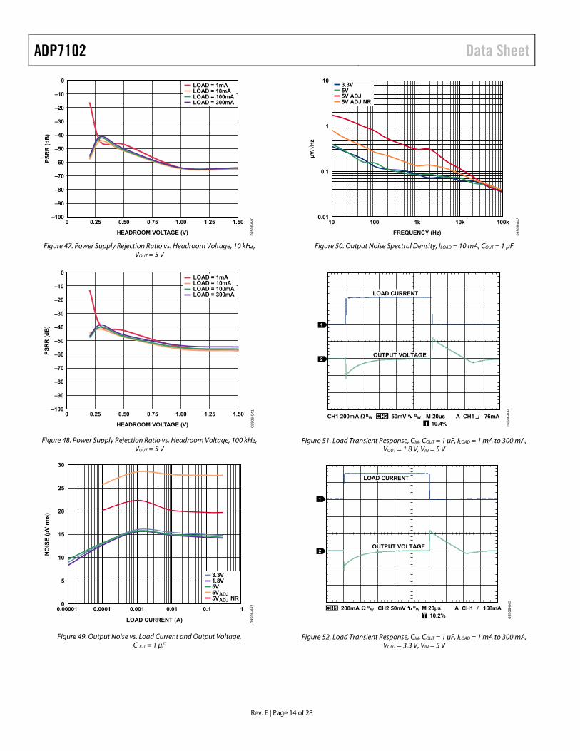
Figure 47. Power Supply Rejection Ratio vs. Headroom Voltage, 10 kHz, VOUT = 5 V
–100
–90
–80
–70
–60
–50
–40
–30
–20
–10
0
0 0.25 0.50 0.75 1.00 1.25 1.50
PS
RR
(d
B)
HEADROOM VOLTAGE (V)
LOAD = 1mALOAD = 10mALOAD = 100mALOAD = 300mA
0950
6-04
1
Figure 48. Power Supply Rejection Ratio vs. Headroom Voltage, 100 kHz, VOUT = 5 V
0
5
10
15
20
25
30
0.00001 0.0001 0.001 0.01 0.1 1
NO
ISE
(µ
V r
ms)
LOAD CURRENT (A)
3.3V1.8V5V5VADJ5VADJ NR
0950
6-04
2
Figure 49. Output Noise vs. Load Current and Output Voltage, COUT = 1 μF
0.01
0.1
1
10
10 100 1k 10k 100k
FREQUENCY (Hz)
3.3V5V5V ADJ5V ADJ NR
µV
/√H
z
0950
6-04
3
Figure 50. Output Noise Spectral Density, ILOAD = 10 mA, COUT = 1 μF
CH2 50mVCH1 200mA M 20µs A CH1 76mA
1
2
T 10.4%Ω B
WB
W
0950
6-04
4
LOAD CURRENT
OUTPUT VOLTAGE
Figure 51. Load Transient Response, CIN, COUT = 1 μF, ILOAD = 1 mA to 300 mA, VOUT = 1.8 V, VIN = 5 V
CH1 200mA CH2 50mV M 20µs A CH1 168mA
1
2
T 10.2%
BW
BWΩ
0950
6-04
5
LOAD CURRENT
OUTPUT VOLTAGE
Figure 52. Load Transient Response, CIN, COUT = 1 μF, ILOAD = 1 mA to 300 mA, VOUT = 3.3 V, VIN = 5 V
Data Sheet ADP7102
Rev. E | Page 15 of 28
CH1 200mA CH2 50mV M 20µs A CH1 216mA
1
2
T 10.2%
BW
BWΩ
0950
6-04
6
LOAD CURRENT
OUTPUT VOLTAGE
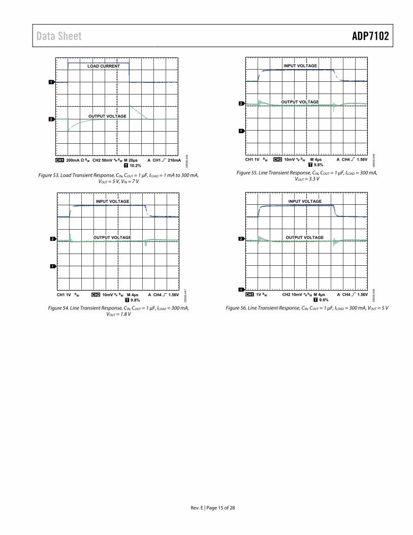
Figure 53. Load Transient Response, CIN, COUT = 1 μF, ILOAD = 1 mA to 300 mA, VOUT = 5 V, VIN = 7 V
CH2 10mVCH1 1V M 4µs A CH4 1.56V
1
2
T 9.8%
BW
BW
0950
6-04
7
OUTPUT VOLTAGE
INPUT VOLTAGE
Figure 54. Line Transient Response, CIN, COUT = 1 μF, ILOAD = 300 mA, VOUT = 1.8 V
CH2 10mVCH1 1V M 4µs A CH4 1.56V
1
2
T 9.8%
BW
BW
0950
6-04
8
OUTPUT VOLTAGE
INPUT VOLTAGE
Figure 55. Line Transient Response, CIN, COUT = 1 μF, ILOAD = 300 mA, VOUT = 3.3 V
CH1 1V CH2 10mV M 4µs A CH4 1.56V1
2
T 9.8%
BW
BW
0950
6-04
9
OUTPUT VOLTAGE
INPUT VOLTAGE
Figure 56. Line Transient Response, CIN, COUT = 1 μF, ILOAD = 300 mA, VOUT = 5 V
ADP7102 Data Sheet
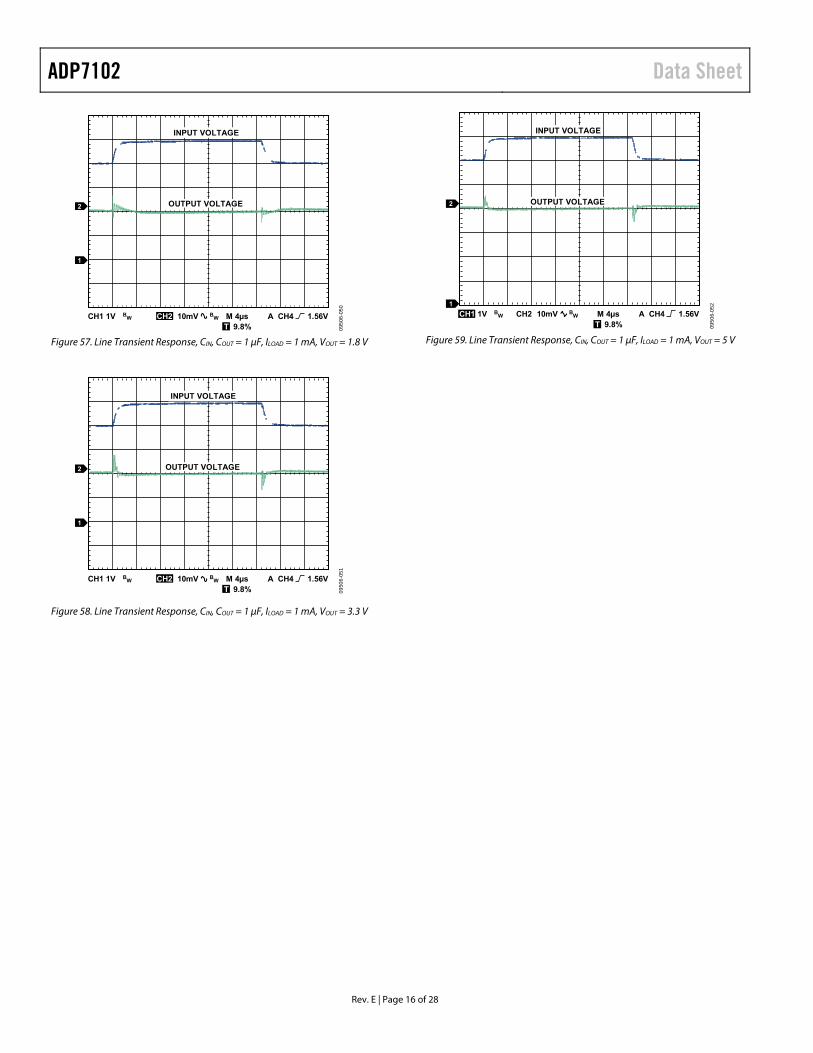
Rev. E | Page 16 of 28
CH2 10mVCH1 1V M 4µs A CH4 1.56V
1
2
T 9.8%
BW
BW
0950
6-05
0
OUTPUT VOLTAGE
INPUT VOLTAGE
Figure 57. Line Transient Response, CIN, COUT = 1 μF, ILOAD = 1 mA, VOUT = 1.8 V
CH2 10mVCH1 1V M 4µs A CH4 1.56V
1
2
T 9.8%
BW
BW
0950
6-05
1
OUTPUT VOLTAGE
INPUT VOLTAGE
Figure 58. Line Transient Response, CIN, COUT = 1 μF, ILOAD = 1 mA, VOUT = 3.3 V
CH2 10mV M 4µs A CH4 1.56V1
2
T 9.8%
BW
BWCH1 1V
0950
6-05
2
OUTPUT VOLTAGE
INPUT VOLTAGE
Figure 59. Line Transient Response, CIN, COUT = 1 μF, ILOAD = 1 mA, VOUT = 5 V
Data Sheet ADP7102
Rev. E | Page 17 of 28
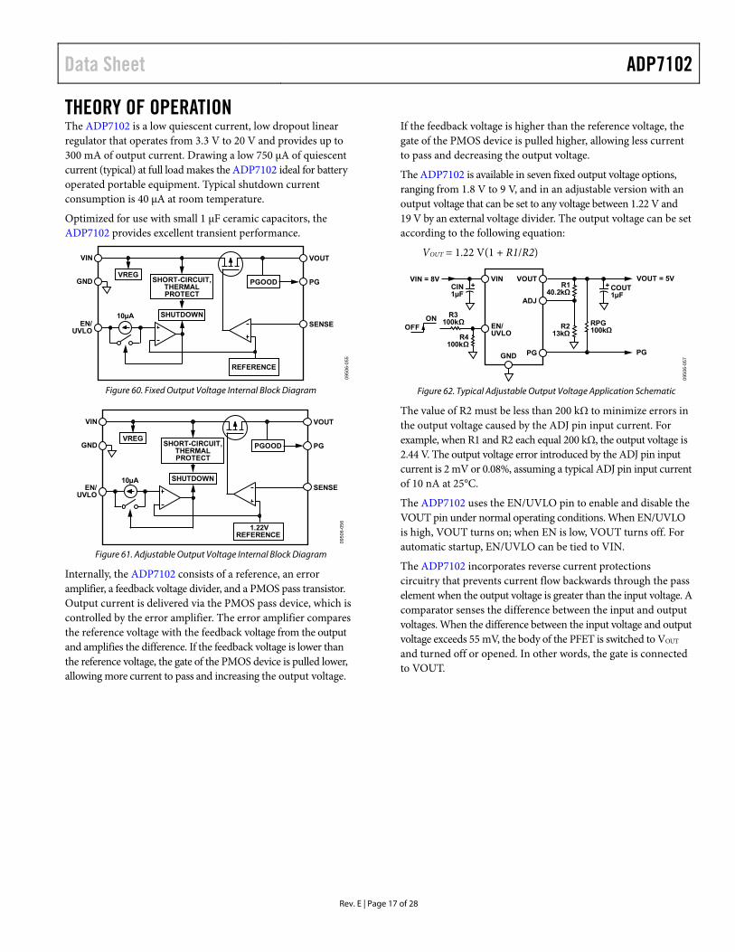
THEORY OF OPERATION The ADP7102 is a low quiescent current, low dropout linear regulator that operates from 3.3 V to 20 V and provides up to 300 mA of output current. Drawing a low 750 μA of quiescent current (typical) at full load makes the ADP7102 ideal for battery operated portable equipment. Typical shutdown current consumption is 40 μA at room temperature.
Optimized for use with small 1 μF ceramic capacitors, the ADP7102 provides excellent transient performance.
SHUTDOWN
VIN
GND
EN/UVLO
VOUT
REFERENCE
VREGPGOOD PG
SENSE
SHORT-CIRCUIT,THERMALPROTECT
10µA
0950
6-05
5
Figure 60. Fixed Output Voltage Internal Block Diagram
SHUTDOWN
VIN
GND
EN/UVLO
VOUT
1.22VREFERENCE
VREGPGOOD PG
SENSE
SHORT-CIRCUIT,THERMALPROTECT
10µA
0950
6-05
6
Figure 61. Adjustable Output Voltage Internal Block Diagram
Internally, the ADP7102 consists of a reference, an error amplifier, a feedback voltage divider, and a PMOS pass transistor. Output current is delivered via the PMOS pass device, which is controlled by the error amplifier. The error amplifier compares the reference voltage with the feedback voltage from the output and amplifies the difference. If the feedback voltage is lower than the reference voltage, the gate of the PMOS device is pulled lower, allowing more current to pass and increasing the output voltage.
If the feedback voltage is higher than the reference voltage, the gate of the PMOS device is pulled higher, allowing less current to pass and decreasing the output voltage.
The ADP7102 is available in seven fixed output voltage options, ranging from 1.8 V to 9 V, and in an adjustable version with an output voltage that can be set to any voltage between 1.22 V and 19 V by an external voltage divider. The output voltage can be set according to the following equation:
VOUT = 1.22 V(1 + R1/R2)
VOUT = 5VVIN = 8V
PG
VOUTVIN
PGGND
ADJ
EN/UVLO
RPG100kΩ
R4100kΩ
R3100kΩ
COUT1µF
CIN1µF
ONOFF R2
13kΩ
++ R140.2kΩ
0950
6-05
7
Figure 62. Typical Adjustable Output Voltage Application Schematic
The value of R2 must be less than 200 kΩ to minimize errors in the output voltage caused by the ADJ pin input current. For example, when R1 and R2 each equal 200 kΩ, the output voltage is 2.44 V. The output voltage error introduced by the ADJ pin input current is 2 mV or 0.08%, assuming a typical ADJ pin input current of 10 nA at 25°C.
The ADP7102 uses the EN/UVLO pin to enable and disable the VOUT pin under normal operating conditions. When EN/UVLO is high, VOUT turns on; when EN is low, VOUT turns off. For automatic startup, EN/UVLO can be tied to VIN.
The ADP7102 incorporates reverse current protections circuitry that prevents current flow backwards through the pass element when the output voltage is greater than the input voltage. A comparator senses the difference between the input and output voltages. When the difference between the input voltage and output voltage exceeds 55 mV, the body of the PFET is switched to VOUT and turned off or opened. In other words, the gate is connected to VOUT.
ADP7102 Data Sheet
Rev. E | Page 18 of 28
APPLICATIONS INFORMATION CAPACITOR SELECTION Output Capacitor
The ADP7102 is designed for operation with small, space-saving ceramic capacitors but functions with most commonly used capacitors as long as care is taken with regard to the effective series resistance (ESR) value. The ESR of the output capacitor affects the stability of the LDO control loop. A minimum of 1 μF capacitance with an ESR of 0.2 Ω or less is recommended to ensure the stability of the ADP7102. Transient response to changes in load current is also affected by output capacitance. Using a larger value of output capacitance improves the transient response of the ADP7102 to large changes in load current. Figure 63 shows the transient responses for an output capacitance value of 1 μF.
CH2 50mVCH1 200mA M 20µs A CH1 76mA
1
2
T 10.4%Ω B
WB
W
0950
6-05
8
LOAD CURRENT
OUTPUT VOLTAGE
Figure 63. Output Transient Response, VOUT = 1.8 V, COUT = 1 μF
Input Bypass Capacitor
Connecting a 1 μF capacitor from VIN to GND reduces the circuit sensitivity to PCB layout, especially when long input traces or high source impedance are encountered. If greater than 1 μF of output capacitance is required, the input capacitor should be increased to match it.
Input and Output Capacitor Properties
Any good quality ceramic capacitors can be used with the ADP7102, as long as they meet the minimum capacitance and maximum ESR requirements. Ceramic capacitors are manufac-tured with a variety of dielectrics, each with different behavior over temperature and applied voltage. Capacitors must have a dielectric adequate to ensure the minimum capacitance over the necessary temperature range and dc bias conditions. X5R or X7R dielectrics with a voltage rating of 6.3 V to 50 V are recommended. Y5V and Z5U dielectrics are not recommended, due to their poor temperature and dc bias characteristics.
Figure 64 depicts the capacitance vs. voltage bias characteristic of an 0402, 1 μF, 10 V, X5R capacitor. The voltage stability of a capacitor is strongly influenced by the capacitor size and voltage rating. In general, a capacitor in a larger package or higher voltage rating exhibits better stability. The temperature variation of the X5R dielectric is ~ ±15% over the −40°C to +85°C temperature range and is not a function of package or voltage rating.
1.2
1.0
0.8
0.6
0.4
0.2
00 2 4 6 8 10
CA
PA
CIT
AN
CE
(µ
F)
VOLTAGE (V) 0950
6-05
9
Figure 64. Capacitance vs. Voltage Characteristic
Use Equation 1 to determine the worst case capacitance accounting for capacitor variation over temperature, component tolerance, and voltage.
CEFF = CBIAS × (1 − TEMPCO) × (1 − TOL) (1)
where: CBIAS is the effective capacitance at the operating voltage. TEMPCO is the worst case capacitor temperature coefficient. TOL is the worst case component tolerance.
In this example, the worst case temperature coefficient (TEMPCO) over −40°C to +85°C is assumed to be 15% for an X5R dielectric. The tolerance of the capacitor (TOL) is assumed to be 10%, and CBIAS is 0.94 μF at 1.8 V, as shown in Figure 64.
Substituting these values in Equation 1 yields
CEFF = 0.94 μF × (1 − 0.15) × (1 − 0.1) = 0.719 μF
Therefore, the capacitor chosen in this example meets the minimum capacitance requirement of the LDO over temperature and tolerance at the chosen output voltage.
To guarantee the performance of the ADP7102, it is imperative that the effects of dc bias, temperature, and tolerances on the behavior of the capacitors be evaluated for each application.
Data Sheet ADP7102
Rev. E | Page 19 of 28
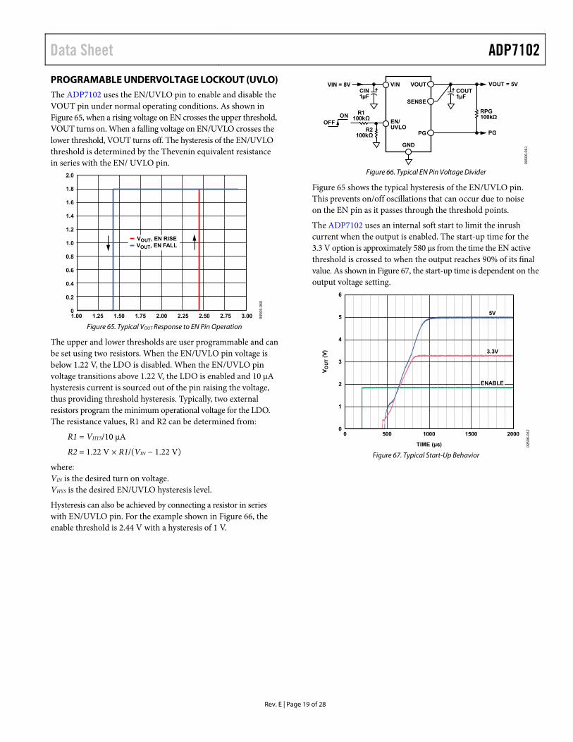
PROGRAMABLE UNDERVOLTAGE LOCKOUT (UVLO) The ADP7102 uses the EN/UVLO pin to enable and disable the VOUT pin under normal operating conditions. As shown in Figure 65, when a rising voltage on EN crosses the upper threshold, VOUT turns on. When a falling voltage on EN/UVLO crosses the lower threshold, VOUT turns off. The hysteresis of the EN/UVLO threshold is determined by the Thevenin equivalent resistance in series with the EN/ UVLO pin.
2.0
1.8
1.6
1.4
1.2
1.0
0.8
0.6
0.4
0.2
1.25 1.50 1.75 2.00 2.25 2.50 2.75 3.001.000
VOUT, EN RISEVOUT, EN FALL
0950
6-06
0
Figure 65. Typical VOUT Response to EN Pin Operation
The upper and lower thresholds are user programmable and can be set using two resistors. When the EN/UVLO pin voltage is below 1.22 V, the LDO is disabled. When the EN/UVLO pin voltage transitions above 1.22 V, the LDO is enabled and 10 μA hysteresis current is sourced out of the pin raising the voltage, thus providing threshold hysteresis. Typically, two external resistors program the minimum operational voltage for the LDO. The resistance values, R1 and R2 can be determined from:
R1 = VHYS/10 μA
R2 = 1.22 V × R1/(VIN − 1.22 V)
where: VIN is the desired turn on voltage. VHYS is the desired EN/UVLO hysteresis level.
Hysteresis can also be achieved by connecting a resistor in series with EN/UVLO pin. For the example shown in Figure 66, the enable threshold is 2.44 V with a hysteresis of 1 V.
VOUT = 5VVIN = 8V
PG
VOUTVIN
PG
GND
SENSE
EN/UVLO
RPG100kΩ
R2100kΩ
R1100kΩ
COUT1µF
CIN1µF
ONOFF
++
0950
6-06
1
Figure 66. Typical EN Pin Voltage Divider
Figure 65 shows the typical hysteresis of the EN/UVLO pin. This prevents on/off oscillations that can occur due to noise on the EN pin as it passes through the threshold points.
The ADP7102 uses an internal soft start to limit the inrush current when the output is enabled. The start-up time for the 3.3 V option is approximately 580 μs from the time the EN active threshold is crossed to when the output reaches 90% of its final value. As shown in Figure 67, the start-up time is dependent on the output voltage setting.
TIME (µs)
0 500 1000 1500 2000
6
4
5
3
2
1
0
VO
UT (
V)
5V
3.3V
ENABLE
0950
6-06
2
Figure 67. Typical Start-Up Behavior
ADP7102 Data Sheet
Rev. E | Page 20 of 28
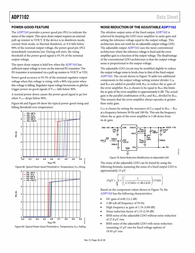
POWER-GOOD FEATURE The ADP7102 provides a power-good pin (PG) to indicate the status of the output. This open-drain output requires an external pull-up resistor to VOUT. If the device is in shutdown mode, current-limit mode, or thermal shutdown, or if it falls below 90% of the nominal output voltage, the power-good pin (PG) immediately transitions low. During soft start, the rising threshold of the power-good signal is 93.5% of the nominal output voltage.
The open-drain output is held low when the ADP7102 has sufficient input voltage to turn on the internal PG transistor. The PG transistor is terminated via a pull-up resistor to VOUT or VIN.
Power-good accuracy is 93.5% of the nominal regulator output voltage when this voltage is rising, with a 90% trip point when this voltage is falling. Regulator input voltage brownouts or glitches trigger power no good signals if VOUT falls below 90%.
A normal power-down causes the power-good signal to go low when VOUT drops below 90%.
Figure 68 and Figure 69 show the typical power-good rising and falling threshold over temperature.
0
1
2
3
4
5
6
4.2 4.3 4.4 4.5 4.6 4.7 4.8 4.9 5.0
PG
(V
)
VOUT (V)
PG –40°CPG –5°CPG +25°CPG +85°CPG +125°C
0950
6-06
3
Figure 68. Typical Power-Good Threshold vs. Temperature, VOUT Rising
0
1
2
3
4
5
6
4.2 4.3 4.4 4.5 4.6 4.7 4.8 4.9 5.0
PG
(V
)
VOUT (V)
PG –40°CPG –5°CPG +25°CPG +85°CPG +125°C
0950
6-06
4
Figure 69. Typical Power-Good Threshold vs. Temperature, VOUT Falling
NOISE REDUCTION OF THE ADJUSTABLE ADP7102 The ultralow output noise of the fixed output ADP7102 is achieved by keeping the LDO error amplifier in unity gain and setting the reference voltage equal to the output voltage. This architecture does not work for an adjustable output voltage LDO. The adjustable output ADP7102 uses the more conventional architecture where the reference voltage is fixed and the error amplifier gain is a function of the output voltage. The disadvantage of the conventional LDO architecture is that the output voltage noise is proportional to the output voltage.
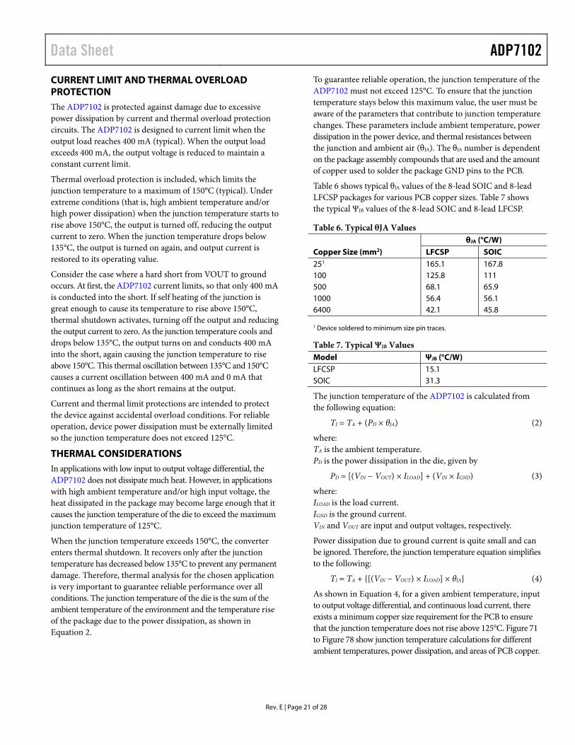
The adjustable LDO circuit may be modified slightly to reduce the output voltage noise to levels close to that of the fixed output ADP7102. The circuit shown in Figure 70 adds two additional components to the output voltage setting resistor divider. CNR and RNR are added in parallel with RFB1 to reduce the ac gain of the error amplifier. RNR is chosen to be equal to RFB2; this limits the ac gain of the error amplifier to approximately 6 dB. The actual gain is the parallel combination of RNR and RFB1, divided by RFB2. This ensures that the error amplifier always operates at greater than unity gain.
CNR is chosen by setting the reactance of CNR equal to RFB1 − RNR at a frequency between 50 Hz and 100 Hz. This sets the frequency where the ac gain of the error amplifier is 3 dB down from its dc gain.
VOUT = 5VVIN = 8V
PG
VOUTVIN
PGGND
ADJ
EN/UVLO
100kΩ
100kΩ
100kΩ
COUT1µF
CIN1µF
ONOFF
RNR13kΩRFB2
13kΩ
++ RFB140.2kΩ CNR
100nF+
0950
6-06
5
Figure 70. Noise Reduction Modification to Adjustable LDO
The noise of the adjustable LDO can be found by using the following formula, assuming the noise of a fixed output LDO is approximately 15 μV.
kΩ13/
k2.40/1kΩ13/11
1μV15
Based on the component values shown in Figure 70, the ADP7102 has the following characteristics:
DC gain of 4.09 (12.2 dB) 3 dB roll off frequency of 59 Hz High frequency ac gain of 1.76 (4.89 dB) Noise reduction factor of 1.33 (2.59 dB) RMS noise of the adjustable LDO without noise reduction
of 27.8 μV rms RMS noise of the adjustable LDO with noise reduction
(assuming 15 μV rms for fixed voltage option) of 19.95 μV rms
Data Sheet ADP7102
Rev. E | Page 21 of 28
CURRENT LIMIT AND THERMAL OVERLOAD PROTECTION The ADP7102 is protected against damage due to excessive power dissipation by current and thermal overload protection circuits. The ADP7102 is designed to current limit when the output load reaches 400 mA (typical). When the output load exceeds 400 mA, the output voltage is reduced to maintain a constant current limit.
Thermal overload protection is included, which limits the junction temperature to a maximum of 150°C (typical). Under extreme conditions (that is, high ambient temperature and/or high power dissipation) when the junction temperature starts to rise above 150°C, the output is turned off, reducing the output current to zero. When the junction temperature drops below 135°C, the output is turned on again, and output current is restored to its operating value.
Consider the case where a hard short from VOUT to ground occurs. At first, the ADP7102 current limits, so that only 400 mA is conducted into the short. If self heating of the junction is great enough to cause its temperature to rise above 150°C, thermal shutdown activates, turning off the output and reducing the output current to zero. As the junction temperature cools and drops below 135°C, the output turns on and conducts 400 mA into the short, again causing the junction temperature to rise above 150°C. This thermal oscillation between 135°C and 150°C causes a current oscillation between 400 mA and 0 mA that continues as long as the short remains at the output.
Current and thermal limit protections are intended to protect the device against accidental overload conditions. For reliable operation, device power dissipation must be externally limited so the junction temperature does not exceed 125°C.
THERMAL CONSIDERATIONS In applications with low input to output voltage differential, the ADP7102 does not dissipate much heat. However, in applications with high ambient temperature and/or high input voltage, the heat dissipated in the package may become large enough that it causes the junction temperature of the die to exceed the maximum junction temperature of 125°C.
When the junction temperature exceeds 150°C, the converter enters thermal shutdown. It recovers only after the junction temperature has decreased below 135°C to prevent any permanent damage. Therefore, thermal analysis for the chosen application is very important to guarantee reliable performance over all conditions. The junction temperature of the die is the sum of the ambient temperature of the environment and the temperature rise of the package due to the power dissipation, as shown in Equation 2.
To guarantee reliable operation, the junction temperature of the ADP7102 must not exceed 125°C. To ensure that the junction temperature stays below this maximum value, the user must be aware of the parameters that contribute to junction temperature changes. These parameters include ambient temperature, power dissipation in the power device, and thermal resistances between the junction and ambient air (θJA). The θJA number is dependent on the package assembly compounds that are used and the amount of copper used to solder the package GND pins to the PCB.
Table 6 shows typical θJA values of the 8-lead SOIC and 8-lead LFCSP packages for various PCB copper sizes. Table 7 shows the typical ΨJB values of the 8-lead SOIC and 8-lead LFCSP.
Table 6. Typical θJA Values
Copper Size (mm2) θJA (°C/W)
LFCSP SOIC 251 165.1 167.8 100 125.8 111 500 68.1 65.9 1000 56.4 56.1 6400 42.1 45.8
1 Device soldered to minimum size pin traces.
Table 7. Typical ΨJB Values Model ΨJB (°C/W) LFCSP 15.1 SOIC 31.3
The junction temperature of the ADP7102 is calculated from the following equation:
TJ = TA + (PD × θJA) (2)
where: TA is the ambient temperature. PD is the power dissipation in the die, given by
PD = [(VIN − VOUT) × ILOAD] + (VIN × IGND) (3)
where: ILOAD is the load current. IGND is the ground current. VIN and VOUT are input and output voltages, respectively.
Power dissipation due to ground current is quite small and can be ignored. Therefore, the junction temperature equation simplifies to the following:
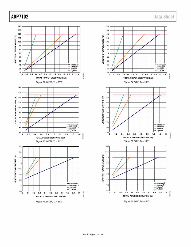
TJ = TA + [(VIN − VOUT) × ILOAD] × θJA (4)
As shown in Equation 4, for a given ambient temperature, input to output voltage differential, and continuous load current, there exists a minimum copper size requirement for the PCB to ensure that the junction temperature does not rise above 125°C. Figure 71 to Figure 78 show junction temperature calculations for different ambient temperatures, power dissipation, and areas of PCB copper.
ADP7102 Data Sheet
Rev. E | Page 22 of 28
25
35
45
55
65
75
85
95
105
115
125
135
145
0 0.2 0.4 0.6 0.8 1.0 1.2 1.4 1.6 1.8 2.0 2.2 2.4
JUN
CT
ION
TE
MP
ER
AT
UR
E (
°C)
TOTAL POWER DISSIPATION (W)
6400mm2
500mm2
25mm2
TJ MAX
0950
6-06
6Figure 71. LFCSP, TA = 25°C
JUN
CT
ION
TE
MP
ER
AT
UR
E (
°C)
50
60
70
80
90
100
110
120
130
140
0 0.2 0.4 0.6 0.8 1.0 1.2 1.4 1.6 1.8
TOTAL POWER DISSIPATION (W)
6400mm2
500mm2
25mm2
TJ MAX
0950
6-06
7
Figure 72. LFCSP, TA = 50°C
JUN
CT
ION
TE
MP
ER
AT
UR
E (
°C)
65
75
85
95
105
115
125
135
145
0 0.1 0.2 0.3 0.4 0.5 0.6 0.7 0.8 0.9 1.0
TOTAL POWER DISSIPATION (W)
6400mm2
500mm2
25mm2
TJ MAX
0950
6-06
8
Figure 73. LFCSP, TA = 85°C
25
35
45
55
65
75
85
95
105
115
125
135
145
0 0.2 0.4 0.6 0.8 1.0 1.2 1.4 1.6 1.8 2.0 2.2 2.4
TOTAL POWER DISSIPATION (W)
JUN
CT
ION
TE
MP
ER
AT
UR
E (
°C)
6400mm2
500mm2
25mm2
TJ MAX
0950
6-06
9
Figure 74. SOIC, TA = 25°C
50
60
70
80
90
100
110
120
130
140
0 0.2 0.4 0.6 0.8 1.0 1.2 1.4 1.6 1.8
TOTAL POWER DISSIPATION (W)
JUN
CT
ION
TE
MP
ER
AT
UR
E (
°C)
6400mm2
500mm2
25mm2
TJ MAX
0950
6-07
0
Figure 75. SOIC, TA = 50°C
65
75
85
95
105
115
125
135
145
0 0.1 0.2 0.3 0.4 0.5 0.6 0.7 0.8 0.9 1.0
TOTAL POWER DISSIPATION (W)
JUN
CT
ION
TE
MP
ER
AT
UR
E (
°C)
6400mm2
500mm2
25mm2
TJ MAX
0950
6-07
1
Figure 76. SOIC, TA = 85°C
Data Sheet ADP7102
Rev. E | Page 23 of 28
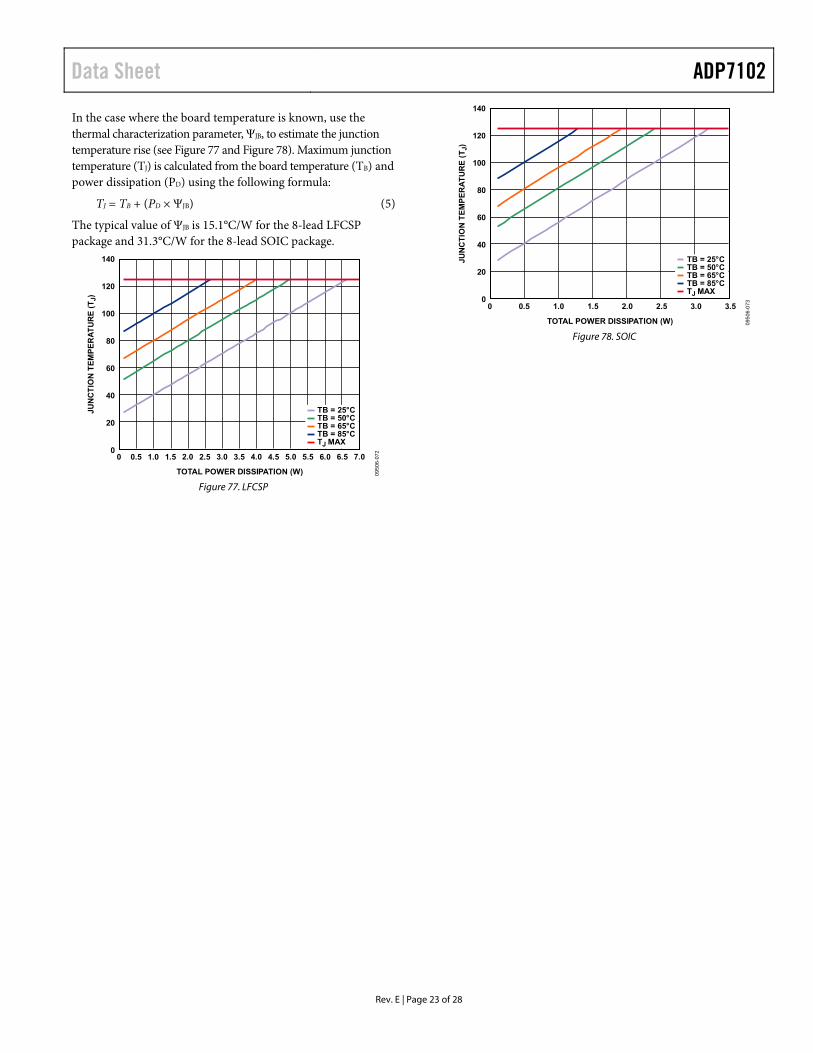
In the case where the board temperature is known, use the thermal characterization parameter, ΨJB, to estimate the junction temperature rise (see Figure 77 and Figure 78). Maximum junction temperature (TJ) is calculated from the board temperature (TB) and power dissipation (PD) using the following formula:
TJ = TB + (PD × ΨJB) (5)
The typical value of ΨJB is 15.1°C/W for the 8-lead LFCSP package and 31.3°C/W for the 8-lead SOIC package.
TOTAL POWER DISSIPATION (W)
JUN
CT
ION
TE
MP
ER
AT
UR
E (
TJ)
0
20
40
60
80
100
120
140
0 0.5 1.0 1.5 2.0 2.5 3.0 3.5 4.0 4.5 5.0 5.5 6.0 6.5 7.0
TB = 25°CTB = 50°CTB = 65°CTB = 85°CTJ MAX
0950
6-07
2
Figure 77. LFCSP
TOTAL POWER DISSIPATION (W)
JUN
CT
ION
TE
MP
ER
AT
UR
E (
TJ)
0
20
40
60
80
100
120
140
0 0.5 1.0 1.5 2.0 2.5 3.0 3.5
TB = 25°CTB = 50°CTB = 65°CTB = 85°CTJ MAX
0950
6-07
3
Figure 78. SOIC
ADP7102 Data Sheet
Rev. E | Page 24 of 28
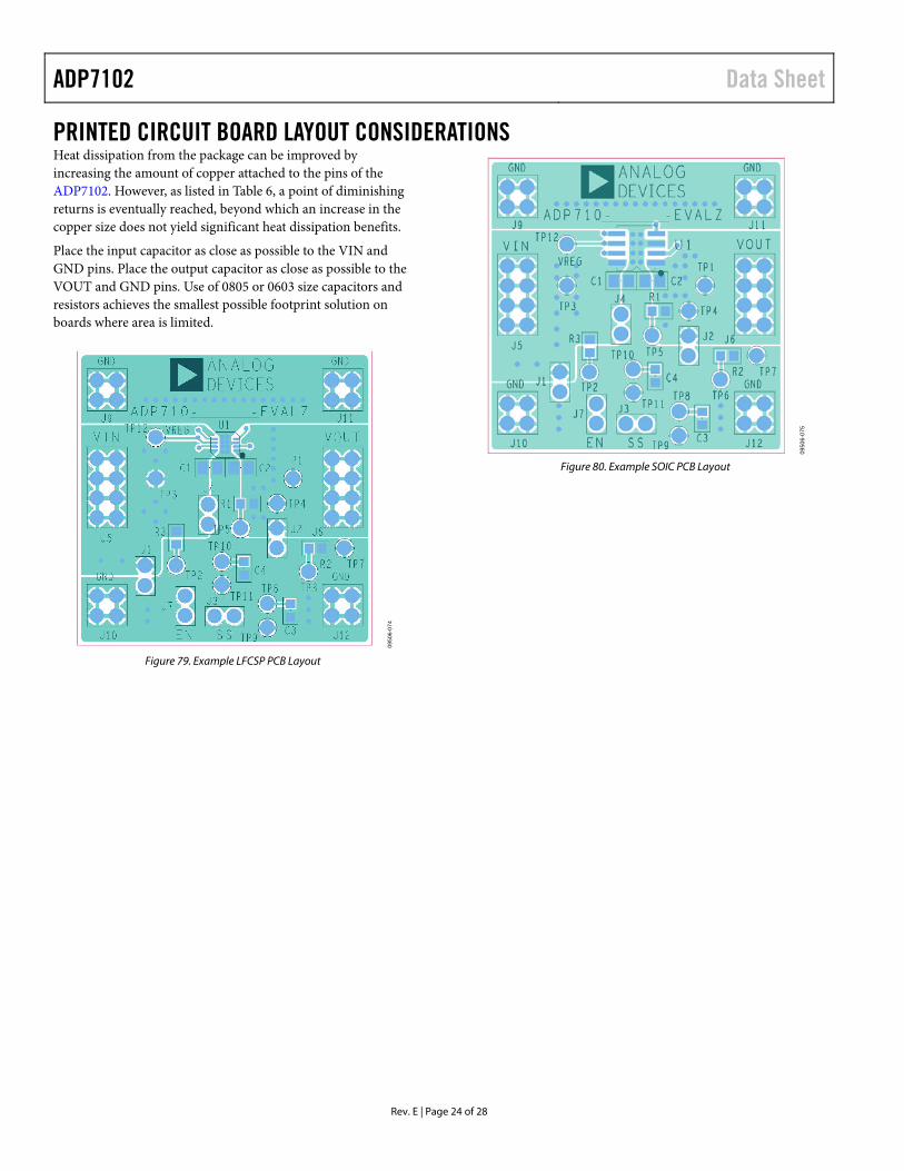
PRINTED CIRCUIT BOARD LAYOUT CONSIDERATIONS Heat dissipation from the package can be improved by increasing the amount of copper attached to the pins of the ADP7102. However, as listed in Table 6, a point of diminishing returns is eventually reached, beyond which an increase in the copper size does not yield significant heat dissipation benefits.
Place the input capacitor as close as possible to the VIN and GND pins. Place the output capacitor as close as possible to the VOUT and GND pins. Use of 0805 or 0603 size capacitors and resistors achieves the smallest possible footprint solution on boards where area is limited.
0950
6-07
4
Figure 79. Example LFCSP PCB Layout
0950
6-07
5
Figure 80. Example SOIC PCB Layout
Data Sheet ADP7102
Rev. E | Page 25 of 28
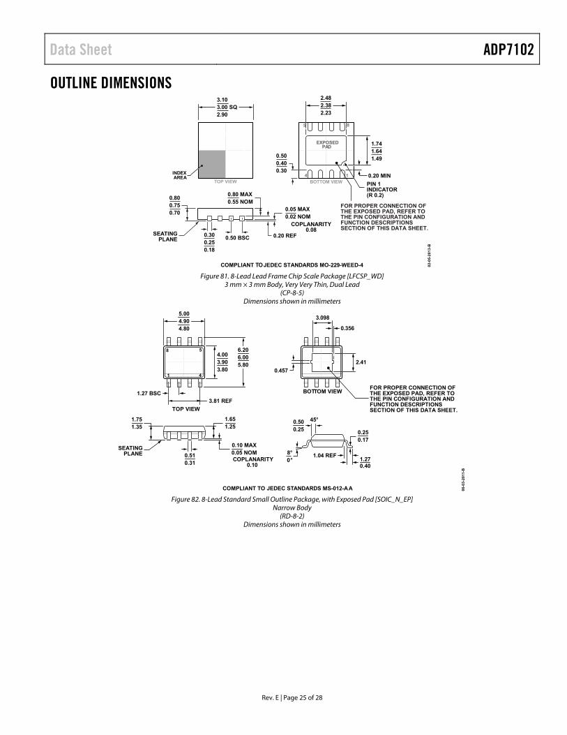
OUTLINE DIMENSIONS
PIN 1INDICATOR(R 0.2)
BOTTOM VIEWTOP VIEW14
85
INDEXAREA
SEATINGPLANE
0.800.750.70
0.300.250.18
0.05 MAX0.02 NOM
0.80 MAX0.55 NOM
0.20 REF0.50 BSC
COPLANARITY0.08
2.482.382.23
1.741.641.490.50
0.400.30
COMPLIANT TOJEDEC STANDARDS MO-229-WEED-4
FOR PROPER CONNECTION OFTHE EXPOSED PAD, REFER TOTHE PIN CONFIGURATION ANDFUNCTION DESCRIPTIONSSECTION OF THIS DATA SHEET.
02-
05-
201
3-B
0.20 MIN
EXPOSEDPAD
3.103.00 SQ2.90
Figure 81. 8-Lead Lead Frame Chip Scale Package [LFCSP_WD]
3 mm × 3 mm Body, Very Very Thin, Dual Lead (CP-8-5)
Dimensions shown in millimeters
COMPLIANT TO JEDEC STANDARDS MS-012-AA 06-
03
-201
1-B
1.270.40
1.751.35
2.41
0.356
0.457
4.003.903.80
6.206.005.80
5.004.904.80
0.10 MAX0.05 NOM
3.81 REF
0.250.17
8°0°
0.500.25
45°
COPLANARITY0.10
1.04 REF
8
1 4
5
1.27 BSC
SEATINGPLANE
FOR PROPER CONNECTION OFTHE EXPOSED PAD, REFER TOTHE PIN CONFIGURATION ANDFUNCTION DESCRIPTIONSSECTION OF THIS DATA SHEET.
BOTTOM VIEW
TOP VIEW
0.510.31
1.651.25
3.098
Figure 82. 8-Lead Standard Small Outline Package, with Exposed Pad [SOIC_N_EP]
Narrow Body (RD-8-2)
Dimensions shown in millimeters
ADP7102 Data Sheet
Rev. E | Page 26 of 28
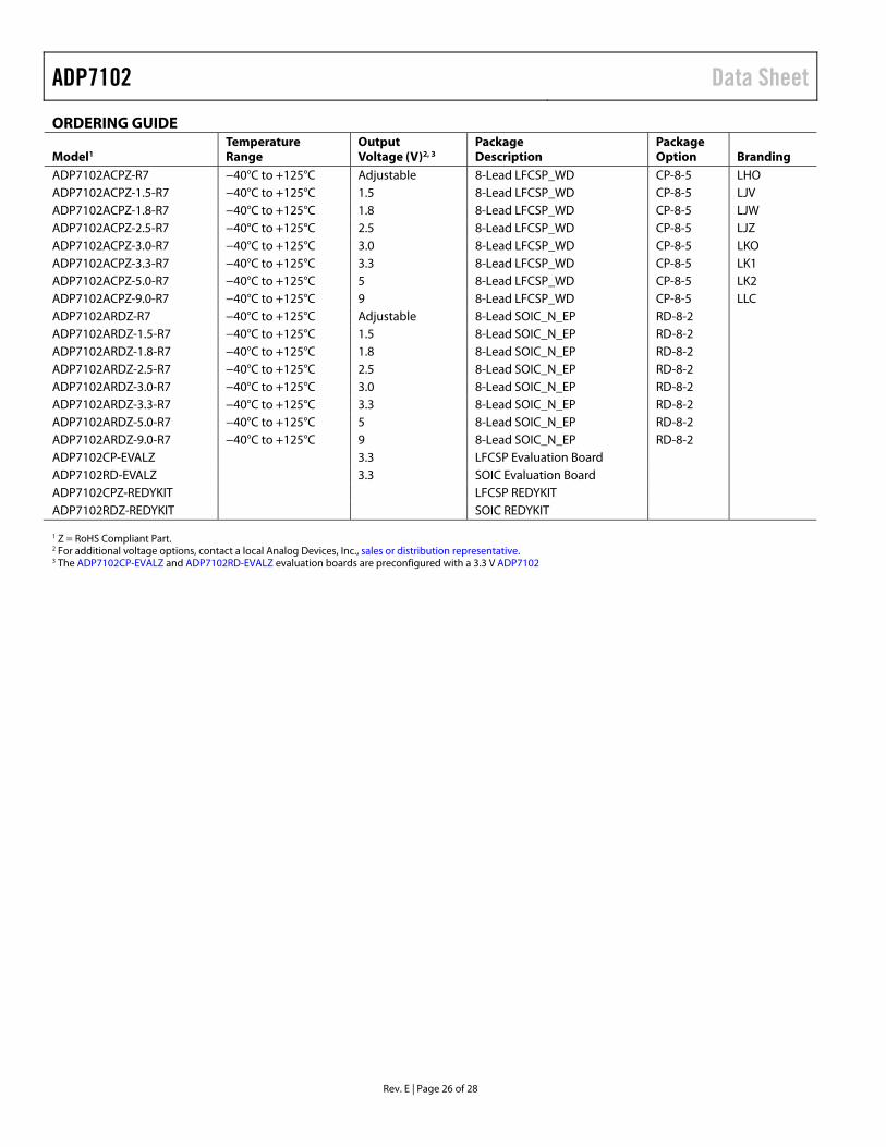
ORDERING GUIDE
Model1 Temperature Range
Output Voltage (V)2, 3
Package Description
Package Option Branding
ADP7102ACPZ-R7 −40°C to +125°C Adjustable 8-Lead LFCSP_WD CP-8-5 LHO ADP7102ACPZ-1.5-R7 −40°C to +125°C 1.5 8-Lead LFCSP_WD CP-8-5 LJV ADP7102ACPZ-1.8-R7 −40°C to +125°C 1.8 8-Lead LFCSP_WD CP-8-5 LJW ADP7102ACPZ-2.5-R7 −40°C to +125°C 2.5 8-Lead LFCSP_WD CP-8-5 LJZ ADP7102ACPZ-3.0-R7 −40°C to +125°C 3.0 8-Lead LFCSP_WD CP-8-5 LKO ADP7102ACPZ-3.3-R7 −40°C to +125°C 3.3 8-Lead LFCSP_WD CP-8-5 LK1 ADP7102ACPZ-5.0-R7 −40°C to +125°C 5 8-Lead LFCSP_WD CP-8-5 LK2 ADP7102ACPZ-9.0-R7 −40°C to +125°C 9 8-Lead LFCSP_WD CP-8-5 LLC ADP7102ARDZ-R7 −40°C to +125°C Adjustable 8-Lead SOIC_N_EP RD-8-2 ADP7102ARDZ-1.5-R7 −40°C to +125°C 1.5 8-Lead SOIC_N_EP RD-8-2 ADP7102ARDZ-1.8-R7 −40°C to +125°C 1.8 8-Lead SOIC_N_EP RD-8-2 ADP7102ARDZ-2.5-R7 −40°C to +125°C 2.5 8-Lead SOIC_N_EP RD-8-2 ADP7102ARDZ-3.0-R7 −40°C to +125°C 3.0 8-Lead SOIC_N_EP RD-8-2 ADP7102ARDZ-3.3-R7 −40°C to +125°C 3.3 8-Lead SOIC_N_EP RD-8-2 ADP7102ARDZ-5.0-R7 −40°C to +125°C 5 8-Lead SOIC_N_EP RD-8-2 ADP7102ARDZ-9.0-R7 −40°C to +125°C 9 8-Lead SOIC_N_EP RD-8-2 ADP7102CP-EVALZ 3.3 LFCSP Evaluation Board ADP7102RD-EVALZ 3.3 SOIC Evaluation Board ADP7102CPZ-REDYKIT LFCSP REDYKIT ADP7102RDZ-REDYKIT SOIC REDYKIT 1 Z = RoHS Compliant Part. 2 For additional voltage options, contact a local Analog Devices, Inc., sales or distribution representative. 3 The ADP7102CP-EVALZ and ADP7102RD-EVALZ evaluation boards are preconfigured with a 3.3 V ADP7102

Data Sheet ADP7102
Rev. E | Page 27 of 28
NOTES
ADP7102 Data Sheet
Rev. E | Page 28 of 28
NOTES
©2011–2015 Analog Devices, Inc. All rights reserved. Trademarks and registered trademarks are the property of their respective owners. D09506-0-9/15(E)